WO2014045372A1 - 半導体記憶装置 - Google Patents
半導体記憶装置 Download PDFInfo
- Publication number
- WO2014045372A1 WO2014045372A1 PCT/JP2012/074080 JP2012074080W WO2014045372A1 WO 2014045372 A1 WO2014045372 A1 WO 2014045372A1 JP 2012074080 W JP2012074080 W JP 2012074080W WO 2014045372 A1 WO2014045372 A1 WO 2014045372A1
- Authority
- WO
- WIPO (PCT)
- Prior art keywords
- transistor
- memory cell
- gate voltage
- signal line
- gate
- Prior art date
- Legal status (The legal status is an assumption and is not a legal conclusion. Google has not performed a legal analysis and makes no representation as to the accuracy of the status listed.)
- Ceased
Links
Images









Classifications
-
- G—PHYSICS
- G11—INFORMATION STORAGE
- G11C—STATIC STORES
- G11C13/00—Digital stores characterised by the use of storage elements not covered by groups G11C11/00, G11C23/00, or G11C25/00
- G11C13/0002—Digital stores characterised by the use of storage elements not covered by groups G11C11/00, G11C23/00, or G11C25/00 using resistive RAM [RRAM] elements
- G11C13/0021—Auxiliary circuits
- G11C13/0061—Timing circuits or methods
-
- G—PHYSICS
- G11—INFORMATION STORAGE
- G11C—STATIC STORES
- G11C13/00—Digital stores characterised by the use of storage elements not covered by groups G11C11/00, G11C23/00, or G11C25/00
- G11C13/0002—Digital stores characterised by the use of storage elements not covered by groups G11C11/00, G11C23/00, or G11C25/00 using resistive RAM [RRAM] elements
- G11C13/0004—Digital stores characterised by the use of storage elements not covered by groups G11C11/00, G11C23/00, or G11C25/00 using resistive RAM [RRAM] elements comprising amorphous/crystalline phase transition cells
-
- G—PHYSICS
- G11—INFORMATION STORAGE
- G11C—STATIC STORES
- G11C13/00—Digital stores characterised by the use of storage elements not covered by groups G11C11/00, G11C23/00, or G11C25/00
- G11C13/0002—Digital stores characterised by the use of storage elements not covered by groups G11C11/00, G11C23/00, or G11C25/00 using resistive RAM [RRAM] elements
- G11C13/0021—Auxiliary circuits
- G11C13/003—Cell access
-
- H—ELECTRICITY
- H10—SEMICONDUCTOR DEVICES; ELECTRIC SOLID-STATE DEVICES NOT OTHERWISE PROVIDED FOR
- H10B—ELECTRONIC MEMORY DEVICES
- H10B63/00—Resistance change memory devices, e.g. resistive RAM [ReRAM] devices
- H10B63/30—Resistance change memory devices, e.g. resistive RAM [ReRAM] devices comprising selection components having three or more electrodes, e.g. transistors
- H10B63/34—Resistance change memory devices, e.g. resistive RAM [ReRAM] devices comprising selection components having three or more electrodes, e.g. transistors of the vertical channel field-effect transistor type
-
- H—ELECTRICITY
- H10—SEMICONDUCTOR DEVICES; ELECTRIC SOLID-STATE DEVICES NOT OTHERWISE PROVIDED FOR
- H10B—ELECTRONIC MEMORY DEVICES
- H10B63/00—Resistance change memory devices, e.g. resistive RAM [ReRAM] devices
- H10B63/80—Arrangements comprising multiple bistable or multi-stable switching components of the same type on a plane parallel to the substrate, e.g. cross-point arrays
- H10B63/84—Arrangements comprising multiple bistable or multi-stable switching components of the same type on a plane parallel to the substrate, e.g. cross-point arrays arranged in a direction perpendicular to the substrate, e.g. 3D cell arrays
-
- H—ELECTRICITY
- H10—SEMICONDUCTOR DEVICES; ELECTRIC SOLID-STATE DEVICES NOT OTHERWISE PROVIDED FOR
- H10B—ELECTRONIC MEMORY DEVICES
- H10B63/00—Resistance change memory devices, e.g. resistive RAM [ReRAM] devices
- H10B63/80—Arrangements comprising multiple bistable or multi-stable switching components of the same type on a plane parallel to the substrate, e.g. cross-point arrays
- H10B63/84—Arrangements comprising multiple bistable or multi-stable switching components of the same type on a plane parallel to the substrate, e.g. cross-point arrays arranged in a direction perpendicular to the substrate, e.g. 3D cell arrays
- H10B63/845—Arrangements comprising multiple bistable or multi-stable switching components of the same type on a plane parallel to the substrate, e.g. cross-point arrays arranged in a direction perpendicular to the substrate, e.g. 3D cell arrays the switching components being connected to a common vertical conductor
-
- G—PHYSICS
- G11—INFORMATION STORAGE
- G11C—STATIC STORES
- G11C13/00—Digital stores characterised by the use of storage elements not covered by groups G11C11/00, G11C23/00, or G11C25/00
- G11C13/0002—Digital stores characterised by the use of storage elements not covered by groups G11C11/00, G11C23/00, or G11C25/00 using resistive RAM [RRAM] elements
- G11C13/0021—Auxiliary circuits
- G11C13/0069—Writing or programming circuits or methods
- G11C2013/0071—Write using write potential applied to access device gate
-
- G—PHYSICS
- G11—INFORMATION STORAGE
- G11C—STATIC STORES
- G11C2213/00—Indexing scheme relating to G11C13/00 for features not covered by this group
- G11C2213/70—Resistive array aspects
- G11C2213/71—Three dimensional array
-
- G—PHYSICS
- G11—INFORMATION STORAGE
- G11C—STATIC STORES
- G11C2213/00—Indexing scheme relating to G11C13/00 for features not covered by this group
- G11C2213/70—Resistive array aspects
- G11C2213/75—Array having a NAND structure comprising, for example, memory cells in series or memory elements in series, a memory element being a memory cell in parallel with an access transistor
-
- G—PHYSICS
- G11—INFORMATION STORAGE
- G11C—STATIC STORES
- G11C2213/00—Indexing scheme relating to G11C13/00 for features not covered by this group
- G11C2213/70—Resistive array aspects
- G11C2213/79—Array wherein the access device being a transistor
-
- H—ELECTRICITY
- H10—SEMICONDUCTOR DEVICES; ELECTRIC SOLID-STATE DEVICES NOT OTHERWISE PROVIDED FOR
- H10N—ELECTRIC SOLID-STATE DEVICES NOT OTHERWISE PROVIDED FOR
- H10N70/00—Solid-state devices having no potential barriers, and specially adapted for rectifying, amplifying, oscillating or switching
- H10N70/20—Multistable switching devices, e.g. memristors
- H10N70/231—Multistable switching devices, e.g. memristors based on solid-state phase change, e.g. between amorphous and crystalline phases, Ovshinsky effect
-
- H—ELECTRICITY
- H10—SEMICONDUCTOR DEVICES; ELECTRIC SOLID-STATE DEVICES NOT OTHERWISE PROVIDED FOR
- H10N—ELECTRIC SOLID-STATE DEVICES NOT OTHERWISE PROVIDED FOR
- H10N70/00—Solid-state devices having no potential barriers, and specially adapted for rectifying, amplifying, oscillating or switching
- H10N70/801—Constructional details of multistable switching devices
- H10N70/821—Device geometry
- H10N70/826—Device geometry adapted for essentially vertical current flow, e.g. sandwich or pillar type devices
-
- H—ELECTRICITY
- H10—SEMICONDUCTOR DEVICES; ELECTRIC SOLID-STATE DEVICES NOT OTHERWISE PROVIDED FOR
- H10N—ELECTRIC SOLID-STATE DEVICES NOT OTHERWISE PROVIDED FOR
- H10N70/00—Solid-state devices having no potential barriers, and specially adapted for rectifying, amplifying, oscillating or switching
- H10N70/801—Constructional details of multistable switching devices
- H10N70/881—Switching materials
- H10N70/882—Compounds of sulfur, selenium or tellurium, e.g. chalcogenides
- H10N70/8828—Tellurides, e.g. GeSbTe
Definitions
- the present invention relates to a semiconductor memory device.
- a resistance change type memory has been studied as a memory to replace a flash memory that is approaching the limit of miniaturization.
- a phase change memory using a chalcogenide (phase change material) such as Ge 2 Sb 2 Te 5 as a resistance change type memory element has been actively studied.
- the state of the phase change material changes to an amorphous state or a crystalline state by Joule heat generated by the applied current.
- the resistance value of the material is high in the amorphous state, and the resistance value of the material is low in the crystalline state. By associating this change in resistance value with information, a function as a memory element can be exhibited.
- the applied current is controlled according to the information to be written.
- the reset operation that is, the operation of writing the bit “0”
- a large current is passed for a short time to dissolve the phase change material, and then the current is rapidly decreased.
- the phase change material is rapidly cooled, and the phase change material changes to an amorphous state having a high resistance.
- the set operation that is, the operation of writing bit '1'
- the phase change material changes to a low resistance crystalline state by flowing a current sufficient to hold the phase change material in a crystallized state for a long time.
- the resistance value of the element is determined by giving a constant potential difference to both ends of the memory element and measuring the current flowing through the element.
- phase change memory when the shape of the memory element is reduced, the current required for changing the state of the phase change material is reduced. For this reason, in principle, it is suitable for miniaturization and multilayering to realize high integration.
- Patent Document 1 describes a structure in which memory cells each composed of a recording layer made of a chalcogenide material and a cell selection diode are stacked via an insulating layer.
- Patent Document 2 a through hole is formed in a stacked body in which a plurality of layers of a gate electrode and a gate insulating film are stacked, and a gate insulating film, a silicon layer serving as a channel, and a chalcogenide layer serving as a recording layer are formed in the through hole.
- a technique is described in which a plurality of memory cells including cell selection transistors and recording elements are stacked in the height direction by being formed on the side surface. By increasing the number of stacked memory cells in the height direction, the area density of the memory cells can be increased and high integration can be realized.
- JP 2009-158020 A WO2011-0745545 gazette
- Patent Document 1 As described in the circuit diagram shown in FIG. 3 and the cross-sectional view shown in FIG. 4 of the same document, between a word line and a bit line that are paths of a write current or a read current, Only one memory cell is connected in the direction normal to the substrate.
- memory cells are multi-layered by stacking layer structures including word lines / memory cells / bit lines.
- the current flowing between the word line and the bit line via the selection transistor of the memory cell is affected by the ON resistance of the selection transistor, causing a voltage drop.
- the source potential varies depending on the layer. Accordingly, assuming that the gate voltage of the memory cell is constant regardless of the layer, the gate-source voltage differs from layer to layer. Thereby, the current for reading / writing information from / to the memory cell varies from layer to layer.
- the present invention has been made in view of the above-described problems, and an object of the present invention is to suppress variation in current supplied to a memory element from layer to layer in a semiconductor memory device in which a plurality of memory cells are connected in series. .
- a semiconductor memory device includes a plurality of memory cells connected in series between a first signal line and a second signal line, and is different for at least two of the selection transistors included in the memory cell. Supply gate voltage.
- the semiconductor memory device of the present invention it is possible to suppress the variation of the current supplied to the memory element from layer to layer.
- FIG. 1 is a diagram illustrating a memory circuit configuration of a semiconductor memory device according to a first embodiment. It is a figure which shows the operation principle in case the memory cell group 4 is comprised by the memory cell 3 of 4 layers.
- FIG. 4 is a diagram illustrating a memory circuit configuration of a semiconductor memory device according to a second embodiment.
- FIG. 6 is a diagram illustrating a memory circuit configuration of a semiconductor memory device according to a third embodiment. It is a figure which shows the operation principle in case the memory cell group 4 is comprised by the memory cell 3 of 4 layers.
- FIG. 6 is a diagram illustrating a memory circuit configuration of a semiconductor memory device according to a fourth embodiment.
- FIG. 9 is a diagram showing a memory circuit configuration of a semiconductor memory device according to a fifth embodiment.
- FIG. 9 is a diagram illustrating a memory circuit configuration of a semiconductor memory device according to a sixth embodiment.
- 3 is a diagram illustrating a circuit example of a voltage converter 6.
- FIG. 4 is a diagram illustrating another circuit example of the voltage converter 6.
- FIG. 3 is a diagram illustrating a circuit of a selection gate driver 5.
- FIG. 4 is a diagram illustrating another circuit example of the selection gate driver 5.
- FIG. 10 is a diagram illustrating a circuit example of a voltage converter 6 according to a ninth embodiment.
- FIG. 10 is a diagram illustrating another circuit example of the voltage converter 6 according to the ninth embodiment. It is a figure which shows the structure of the memory cell array part of a semiconductor memory device.
- each memory cell of the embodiment is formed on a semiconductor substrate such as single crystal silicon by a known integrated circuit technique such as a CMOS (complementary MOS transistor) unless otherwise limited.
- CMOS complementary MOS transistor
- FIG. 1 is a diagram showing a memory circuit configuration of a semiconductor memory device according to Embodiment 1 of the present invention.
- the memory cell 3 has a configuration in which a phase change storage element 1 and a selection transistor 2 are connected in parallel, and both terminals of the storage element 1 are connected to the drain and source of the selection transistor 2.
- the memory cell group 4 has a configuration in which a plurality of memory cells 3 are connected in series between a word line (a signal line having a potential VWL ) and a bit line (a signal line having a potential VBL ).
- the selection gate driver 5 is provided corresponding to each memory cell 3 in each layer, and receives the supply of the input voltage VIN from the voltage converter 6 to drive the selection transistor 2 of each memory cell 3.
- the memory cell group 4 is formed by being laminated in the normal direction on the semiconductor substrate of the semiconductor memory device. Thereby, the number of storage bits per area can be increased as compared with the conventional semiconductor memory device.
- a plurality of memory cell groups 4 are formed on a semiconductor substrate.
- One memory cell group 4 is selected by generating a potential difference between the word line potential V WL and the bit line potential V BL . Further, by changing any one of the potential of the control terminal S 1 ⁇ S n of the select gate driver 5, the only selection transistors 2 corresponding to the layer is cut off, rather than the current selection transistors 2 in the layer It flows through the memory element 1. Thus, information can be selectively written / erased / read with respect to one memory cell.
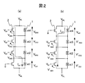
- FIG. 2 is a diagram showing an operation principle when the memory cell group 4 is composed of four layers of memory cells 3.
- 2A shows a state where the memory cell of the storage element st1 is selected
- FIG. 2B shows a state where the memory cell of the storage element st4 is selected. It is assumed that a specific memory cell group 4 is selected by satisfying word line potential VWL> bit line potential VBL.
- the memory element When a large current is passed through the memory element for a short time, the memory element becomes high resistance and erased (reset) to the state of bit '0'. When a small current is passed for a long time, the memory element becomes low resistance and written to the state of bit '1'. It is included (set).
- a potential difference smaller than that at the time of erasing / writing is applied between the word line and the bit line, the difference in resistance value of the storage element is detected by the difference in current value, and the bit value is reproduced. .
- each selection transistor Since each selection transistor has an ON resistance, a voltage drop occurs when the currents I st1 and I st4 flow. Therefore, the source potential of each transistor differs from layer to layer. Therefore, when the gate potentials V G1 to V G4 supplied to the selection transistors of each layer are all the same value, the gate-source voltage V GS of each layer differs from layer to layer. Specifically, V GS4 is the highest, gradually decreases as the bit line is approached, and V GS1 is the lowest. Since the ON resistance of the selection transistor depends on V GS , the ON resistance varies from layer to layer, and as a result, the current flowing through the memory element of each layer varies from layer to layer, which may cause write errors and read errors. Becomes higher.
- the voltage converter 6 and the selection gate driver 5 supply different gate potentials for each memory cell, and the gate-source voltage V GS of each selection transistor becomes the same, so that the current flowing through each storage element is different for each layer. Try to be the same.
- the voltage converter 6 generates voltages V IN1 to V INn corresponding to each layer based on the input voltage V DD and supplies them to the selection gate driver 5 corresponding to each layer.
- Select gate driver 5 receives a logic signal indicating the selection / non-selection of the memory cells from each control terminal S 1 ⁇ S n, and supplies the gate potential V G relative accordingly each of the select transistors.
- the gate potential is set as the ground potential, and when the memory cell is not selected, the input voltage VIN is supplied as the gate potential.
- FIG. 3 is a diagram showing a memory circuit configuration of the semiconductor memory device according to the second embodiment of the present invention.
- m memory cell groups 4 are provided.
- the circuit configuration including the word line / memory cell group 4 / bit line is surrounded by a dotted line so that each memory cell group 4 can be distinguished.
- Each memory cell group 4 can be selected by selectively generating a predetermined potential difference between the word line and the bit line. For example, it is possible to select the memory cell group 4 that extends in the X direction on the substrate, extends the bit line in the Y direction on the substrate, and is arranged at a position where the two intersect. Alternatively, the same effect can be achieved by providing a selection switch between any one of the signal lines and the memory cell group 4.
- each selection gate driver 5 supplies a common gate voltage to selection transistors arranged in the same layer.
- FIG. 4 is a diagram showing a memory circuit configuration of the semiconductor memory device according to the third embodiment of the present invention.
- a delay circuit including a capacitor 7 is provided in parallel with a signal line connecting each selection gate driver 5 and a corresponding selection transistor.
- Other configurations are the same as those of the first embodiment.
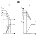
- FIG. 5 is a diagram showing an operation principle when the memory cell group 4 is constituted by four layers of memory cells 3.
- FIG. 5A shows how the gate potential VG falls and the storage element current Ist rises when the capacitor 7 is not provided.
- FIG. 5B shows how the gate voltage VG falls and the storage element current Ist rises when the capacitor 7 is provided.
- the semiconductor memory device supplies different gate potentials VG to the respective layers. Therefore, when the gate potentials VG drop with the same inclination, as shown in FIG. Fall time will be different. That is, the current Ist1 controlled by the lowest gate potential VG1 rises fastest, and the current Ist4 controlled by the highest gate potential VG4 rises latest.
- phase change material changes its state according to the time for supplying current and stores information. Therefore, when the rise time of current differs for each memory cell, the memory element state changes to memory if the layers are controlled in the same way. It will vary from cell to cell, increasing the possibility of bit errors.
- the rise time of the current flowing through each memory cell is made uniform by providing the capacitor 7 and delaying the gate potential that falls quickly. Specifically, the capacity of the capacitor 7 corresponding to the gate potential VG1 that falls the fastest is maximized, the capacity is gradually decreased upward, and the capacity of the capacitor 7 corresponding to the gate potential VG4 is minimized. As a result, as shown in FIG. 5B, the gate potential VG of each layer falls with the same delay time, and thus the current flowing through the storage element also rises with the same delay time.
- the delay time for delaying the fall of the gate potential is provided for each layer, so that the rise time of the current supplied to the memory element can be made uniform for each layer. . Accordingly, it is possible to suppress the variation in the state of the memory element due to the supply of a different current for each memory cell.
- a circuit configuration other than that shown in FIG. 4 can be employed as long as the rising of the current flowing through the memory element can be made uniform by delaying the falling of the gate potential VG.
- the timing of the control signal input to the selection gate driver 5 may be delayed on the control circuit side without changing the falling gradient of the gate potential.
- the timing at which the gate potential VG1 starts to fall may be delayed the latest, and the timing at which the gate potential VG4 starts to fall may be earliest.
- the position where the capacitor 7 and the inductance are provided is not particularly limited, but it is considered that the simplest mounting is provided on the circuit board on which the voltage converter 6 and the selection gate driver 5 are mounted.
- FIG. 6 is a diagram showing a memory circuit configuration of a semiconductor memory device according to Embodiment 4 of the present invention.
- the capacitor 7 described in the third embodiment is arranged in each layer in the circuit configuration described in the second embodiment.
- the voltage converter 6 and the selection gate driver 5 can be shared to reduce the circuit area, and the gate potential fall time can be made uniform for each layer.
- the selection gate driver 5 when used in common for a plurality of memory cell groups 4, parasitic capacitances such as signal lines increase and variation in delay time for each layer increases. Therefore, as described with reference to FIG. The problem is easily manifested. Therefore, the effects of the second embodiment can be utilized by introducing the delay circuit (or the circuit configuration that exhibits the same effect) by the capacitor 7 described in the third embodiment.
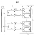
- FIG. 7 is a diagram showing a memory circuit configuration of a semiconductor memory device according to Embodiment 5 of the present invention.
- a common gate voltage is supplied by setting a plurality of adjacent memory cells 3 in the memory cell group 4 as a set.
- the input voltages VIN1 to VINk supplied to the selection gate driver 5 are shared by the voltage output from the output terminal VB1, and the corresponding gate voltages VG1 to VGk are common.
- the input voltages VINn-x to VINn are shared by the voltage output from the output terminal VBj, and the corresponding gate voltages VGn-x to VGn are shared.
- the number of memory cells and the number of sets using the same gate potential may be arbitrary.
- the gate-source voltage varies from layer to layer as described in the first embodiment, and thus the current flowing through the memory element varies from layer to layer.
- the same gate potential is used as shown in FIG. Therefore, by reducing the number of output terminals of the voltage converter 6, the circuit occupation area and power consumption of the voltage converter 6 can be reduced.
- FIG. 8 is a diagram showing a memory circuit configuration of a semiconductor memory device according to Embodiment 6 of the present invention.
- a common gate voltage is supplied by setting a plurality of adjacent memory cells 3 in the memory cell group 4 as a set similarly to the fifth embodiment under the circuit configuration described in the second embodiment. .
- the circuit occupation area of the voltage converter 6 can be reduced by reducing the number of output terminals of the voltage converter 6 while reducing the circuit occupation area and power consumption of the voltage converter 6 and the selection gate driver 5 as in the second embodiment. And power consumption can be reduced.
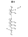
- FIG. 9 is a diagram illustrating a circuit example of the voltage converter 6.
- the voltage converter 6 shown in FIG. 9 includes a plurality of transistors 9 and a current source 8.
- Each transistor 9 forms a diode connection in which the gate terminal and the drain terminal are connected to each other, and a constant voltage is generated between the drain and the source according to the current generated by the current source 8.
- the circuit example shown in FIG. 9 has an advantage that the occupied area is small as compared with a method of generating a potential difference using a resistor.
- the current source 8 can be realized by a general circuit used in a semiconductor integrated circuit.
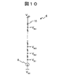
- FIG. 10 is a diagram illustrating another circuit example of the voltage converter 6.
- a voltage converter 6 shown in FIG. 10 includes a plurality of resistors 10 and a current source 8.
- a constant voltage is generated across each resistor 10 in accordance with the current generated by the current source 8.
- a plurality of different voltages can be obtained by extracting the voltage across each resistor 10 to the output terminal.
- the output voltage can be freely designed as compared with the circuit shown in FIG.
- FIG. 11 is a diagram showing a circuit of the selection gate driver 5.
- the selection gate driver 5 shown in FIG. 11 includes NMOS (N-channel Metal Oxide Semiconductor) transistors 11 a and 11 b and an inverter 12.
- the inverter 12 inverts the control voltage and inputs it to the gate terminal of the NMOS transistor 11a.
- a control voltage is input to the gate terminal of the NMOS transistor 11b.
- the control voltage is a high potential indicating memory cell selection
- the NMOD transistor 11a is non-conductive
- the NMOS transistor 11b is conductive
- the output voltage is the ground voltage.
- the selection gate driver 5 can be realized with a small number of elements.
- FIG. 12 is a diagram illustrating another circuit example of the selection gate driver 5.
- the selection gate driver 5 shown in FIG. 12 includes NMOS transistors 11a and 11b, an inverter 12, and a PMOS transistor 13.
- the inverter 12 inverts the control voltage and inputs it to the gate terminal of the NMOS transistor 11a.
- a control voltage is input to the gate terminal of the PMOS transistor 13 and the gate terminal of the NMOS transistor 11b.
- the control voltage is a high potential indicating memory cell selection
- the NMOS transistor 11a and the PMOS transistor are non-conductive
- the NMOS transistor is conductive
- the output voltage is the ground voltage.
- the NMOS transistor 11a and the PMOS transistor 13 are turned on, the NMOS transistor 11b is turned off, and the output voltage is the same as the input voltage.
- the NMOS transistor 11a becomes conductive at an input voltage lower than the threshold voltage, so that an output voltage in a wider range than the circuit shown in FIG. 11 can be provided.
- ⁇ Embodiment 9> The characteristics of the memory cell 3 vary depending on the ambient temperature. In particular, the gate-source voltage necessary for conducting the selection transistor 2 varies depending on the temperature and affects the current flowing through the memory element 1. Therefore, in the ninth embodiment of the present invention, a configuration example is described in which the gate potential VG is adjusted according to the temperature of the selection transistor 2 included in the memory cell 3 to suppress the current flowing through the memory element 1 from fluctuating due to the temperature. To do. Other configurations are the same as those in the first to sixth and eighth embodiments.
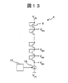
- FIG. 13 is a diagram illustrating a circuit example of the voltage converter 6 according to the ninth embodiment.
- a current source 14 that can control the output voltage is provided instead of the current source 8.
- a temperature detection circuit 15 is connected to the control terminal of the current source 14.
- the temperature detection circuit 15 and the current source 8 can use a circuit configuration similar to a band gap reference (BGR) generally known in a semiconductor integrated circuit.
- BGR band gap reference
- a band gap reference circuit can be used as the temperature detection circuit 15 and a current mirror circuit connected to the band gap reference circuit can be used as the current source 14.
- the temperature detector 15 detects the temperature around the selection transistor 2 and adjusts the output voltage of the current source 14 according to the temperature, whereby the voltage converter 6 outputs the voltage.
- the voltage VIN to be adjusted can be adjusted.
- the current flowing through the memory element 1 can be adjusted in accordance with the gate-source voltage necessary for making the select transistor 2 conductive, and a constant element current can be supplied regardless of the temperature.
- FIG. 14 is a diagram illustrating another circuit example of the voltage converter 6 according to the ninth embodiment.
- the current source 8 in the circuit configuration described in FIG. 10 is replaced with the current source 14, and a temperature detection circuit 15 is connected to the control terminal.
- the resistor having a smaller temperature dependency is used as compared with the diode-connected transistor shown in FIG. 13, variation due to temperature can be further suppressed.
- FIG. 15 is a diagram showing the configuration of the memory cell array portion of the semiconductor memory device according to the present invention.
- FIG. 15A is a schematic three-dimensional view of a part of the semiconductor memory device, and
- FIG. 15B is an XZ sectional view of FIG.
- the electrode 103 extends in the X direction and operates as a bit line (selection electrode) for selecting the phase change memory chain PCMCHAIN including the memory cell group 4 in the Y direction.
- a stacked body in which gate polysilicon layers 121p, 122p, 123p, and 124p, which are gate electrodes of the selection transistor 2, and insulating films 111, 112, 113, 114, and 115 are alternately stacked is disposed.
- a phase change memory chain PCMCHAIN is formed in a hole in the Z direction formed in the stacked body.
- Select transistor STTr Has a gate electrode 181p, a gate insulating film 110, and a channel semiconductor layer 150p. Select transistor STTr.
- Insulating films 171, 172, and 131 are disposed around.
- the plate-like electrode 102 is connected to the selection transistor STTr. It is arranged at the bottom of.
- the N-type semiconductor layer 138p electrically connects the electrode 103 and the PCMCHIAN.
- the insulating film 192 is formed between the electrode 103 and PCMCHIAN.
- the N-type semiconductor layer 160p electrically connects the electrode 102 and the channel semiconductor layer 150p.
- PCMCHAIN formed in the hole in the stack includes a gate insulating film 109, a channel semiconductor layer 108 p, a phase change material layer 107, and an insulating film 191.
- the gate electrodes 181p can be formed at a 2F pitch and a 3F pitch, respectively, where F is the minimum processing dimension. That is, a memory cell having a projected area 6F 2 in the XY plane can be formed.
- phase change material layer 107 for example, a material that stores information using a difference in resistance value in an amorphous state and a resistance value in a crystalline state, such as Ge 2 Sb 2 Te 5, can be used.
- the phase change material in the amorphous state is heated above the crystallization temperature and held for about 10 ⁇ 6 seconds or longer. It implements by making it into a crystalline state.
- the phase change material in the crystalline state can be brought into an amorphous state by heating it to a temperature equal to or higher than the melting point to make it into a liquid state and then rapidly cooling it.
- phase change memory cell SMC surrounded by a dotted line in FIG. 15B corresponds to the memory cell 3.
- the memory element 1 is formed by the phase change material layer 107 of each layer.
- the select transistor 2 is formed by a channel semiconductor layer 108p and gate polysilicon layers 121p to 124p formed on the side surface of the through hole.
- the present invention is not limited to the above-described embodiment, and includes various modifications.
- the above embodiment has been described in detail for easy understanding of the present invention, and is not necessarily limited to the one having all the configurations described.
- a part of the configuration of one embodiment can be replaced with the configuration of another embodiment.
- the configuration of another embodiment can be added to the configuration of a certain embodiment. Further, with respect to a part of the configuration of each embodiment, another configuration can be added, deleted, or replaced.
Landscapes
- Chemical & Material Sciences (AREA)
- Crystallography & Structural Chemistry (AREA)
- Semiconductor Memories (AREA)
Description
図1は、本発明の実施形態1に係る半導体記憶装置のメモリ回路構成を示す図である。メモリセル3は、相変化型記憶素子1と選択トランジスタ2を並列接続した構成を有し、選択トランジスタ2のドレインとソースに記憶素子1の両端子が接続される。メモリセル群4は、ワード線(電位VWLを有する信号線)とビット線(電位VBLを有する信号線)の間に複数のメモリセル3を直列接続した構成を有する。選択ゲートドライバ5は、各層のメモリセル3に対応してそれぞれ設けられており、電圧変換器6から入力電圧VINの供給を受けて各メモリセル3の選択トランジスタ2を駆動する。メモリセル群4は半導体記憶装置の半導体基板上に法線方向に積層して形成される。これにより、従来の半導体記憶装置と比べて面積あたりの記憶ビット数を増加させることができる。
以上のように、本実施形態1に係る半導体記憶装置は、各層のメモリセルの選択トランジスタに対してそれぞれ異なるゲート電圧を供給することにより、記憶素子に流れる電流の層毎のばらつきを低減することができる。
図3は、本発明の実施形態2に係る半導体記憶装置のメモリ回路構成を示す図である。本実施形態2においては、m個のメモリセル群4が設けられている。図3において、記載の便宜上、ワード線/メモリセル群4/ビット線を含む回路構成を点線で囲み、各メモリセル群4を区別できるようにした。
図4は、本発明の実施形態3に係る半導体記憶装置のメモリ回路構成を示す図である。本実施形態3において、各選択ゲートドライバ5と対応する選択トランジスタを結ぶ信号線に対して並列に、コンデンサ7によって構成された遅延回路が設けられている。その他の構成は、実施形態1と同様である。
以上のように、本実施形態3に係る半導体記憶装置は、ゲート電位の立ち下がりを遅延させる遅延回路を層毎に設けることにより、記憶素子に供給する電流の立ち上り時間を各層について揃えることができる。これにより、メモリセル毎に異なる電流が供給されることによって記憶素子の状態がばらつくことを抑えることができる。
図6は、本発明の実施形態4に係る半導体記憶装置のメモリ回路構成を示す図である。本実施形態4においては、実施形態2で説明した回路構成において、実施形態3で説明したコンデンサ7を各層に配置した。これにより、電圧変換器6と選択ゲートドライバ5を共通化して回路面積を抑えつつ、ゲート電位の立ち下がり時間を各層について揃えることができる。
図7は、本発明の実施形態5に係る半導体記憶装置のメモリ回路構成を示す図である。本実施形態5においては、メモリセル群4内の隣接する複数のメモリセル3をセットにして共通のゲート電圧を供給することとした。図7に示す例においては、選択ゲートドライバ5に供給する入力電圧VIN1~VINkは出力端子VB1が出力する電圧をもって共有化し、これらに対応するゲート電圧VG1~VGkは共通になっている。同様に入力電圧VINn-x~VINnは出力端子VBjが出力する電圧をもって共通化し、これらに対応するゲート電圧VGn-x~VGnは共通になっている。同一のゲート電位を用いるメモリセルの個数やセット数は任意でよい。
図8は、本発明の実施形態6に係る半導体記憶装置のメモリ回路構成を示す図である。本実施形態6では、実施形態2で説明した回路構成の下で実施形態5と同様にメモリセル群4内の隣接する複数のメモリセル3をセットにして共通のゲート電圧を供給することとした。これにより、実施形態2と同様に電圧変換器6と選択ゲートドライバ5の回路占有面積および消費電力を小さく抑えつつ、さらに電圧変換器6の出力端子数を減らして電圧変換器6の回路占有面積と消費電力を低減することができる。
本発明の実施形態7では、電圧変換器6の回路例について説明する。その他の構成については実施形態1~6と同様である。
本発明の実施形態8では、選択ゲートドライバ5の回路例について説明する。その他の構成については実施形態1~7と同様である。
メモリセル3の特性は、周囲温度に影響を受けて変動する。特に、選択トランジスタ2を導通させるために必要なゲート-ソース間電圧が温度に応じて変動し、記憶素子1に流れる電流に影響を与える。そこで本発明の実施形態9では、メモリセル3が備える選択トランジスタ2の温度に応じてゲート電位VGを調整することにより、記憶素子1に流れる電流が温度により変動することを抑制する構成例について説明する。その他の構成については実施形態1~6、8と同様である。
本発明の実施形態10では、本発明に係る半導体記憶装置のメモリセル3周辺の具体的な積層構造について説明する。ここでは、ワード線をプレート状に形成してメモリセル群4間で共有し、ビット線と選択トランジスタSttr.によっていずれかのメモリセル群4を選択する構成を例示する。
Claims (12)
- 第1および第2信号線と、
トランジスタと抵抗変化素子を並列接続して構成され、前記抵抗変化素子の状態変化によって情報を記憶するメモリセルと、
前記トランジスタにゲート電圧を供給するドライバ回路と、
を備え、
前記メモリセルは、前記第1および第2信号線の間に複数直列に接続されており、
前記ドライバ回路は、各前記メモリセルが備える前記トランジスタのうちいずれか少なくとも2つ以上について、それぞれ異なるゲート電圧を供給する
ことを特徴とする半導体記憶装置。 - 請求項1において、
前記ドライバ回路は、
各前記メモリセルが備える前記トランジスタに供給するゲート電圧のうち、
前記第1信号線に最も近い位置に配置された前記メモリセルが備える前記トランジスタに対して最も低いゲート電圧を供給し、
前記トランジスタが配置されている位置が前記第2信号線に近くなるにしたがって、前記トランジスタに対して供給するゲート電圧を次第に高くし、
前記第2信号線に最も近い位置に配置された前記メモリセルが備える前記トランジスタに対して最も高いゲート電圧を供給する
ことを特徴とする半導体記憶装置。 - 請求項2において、
前記ドライバ回路は、全ての前記メモリセルが備える前記トランジスタについて、同じ立ち下がり時間でゲート電圧を立ち下げる
ことを特徴とする半導体記憶装置。 - 請求項3において、
前記ドライバ回路は、
各前記メモリセルが備える前記トランジスタに供給するゲート電圧のうち、
前記第1信号線に最も近い位置に配置された前記メモリセルが備える前記トランジスタに対して供給するゲート電圧を最も緩やかに立ち下げ、
前記トランジスタが配置されている位置が前記第2信号線に近くなるにしたがって、前記トランジスタに対して供給するゲート電圧を立ち下げる勾配を次第に大きくし、
前記第2信号線に最も近い位置に配置された前記メモリセルが備える前記トランジスタに対して供給するゲート電圧を最も急峻に立ち下げる
ことを特徴とする半導体記憶装置。 - 請求項3において、
前記ドライバ回路は、各前記メモリセルが備える前記トランジスタのうちいずれか少なくとも2つ以上との間において、前記ゲート電圧を遅延させる遅延回路を備え、
前記遅延回路は、前記ドライバ回路が各前記トランジスタに対して供給するゲート電圧の立ち下がり時間が全て同じになるように構成されている
ことを特徴とする半導体記憶装置。 - 請求項5において、
前記遅延回路は、
各前記メモリセルが備える前記トランジスタに供給するゲート電圧のうち、
前記第1信号線に最も近い位置に配置された前記メモリセルが備える前記トランジスタに対して供給されるゲート電圧が最も緩やかに立ち下がり、
前記トランジスタが配置されている位置が前記第2信号線に近くなるにしたがって、前記トランジスタに対して供給されるゲート電圧が立ち下がる勾配が次第に大きくなり、
前記第2信号線に最も近い位置に配置された前記メモリセルが備える前記トランジスタに対して供給されるゲート電圧が最も急峻に立ち下がる
ように構成されていることを特徴とする半導体記憶装置。 - 請求項6において、
前記遅延回路は、
各前記メモリセルが備える前記トランジスタのうちいずれか少なくとも2つ以上との間においてそれぞれ配置されたコンデンサを用いて構成されており、
各前記コンデンサは、
前記第1信号線に最も近い位置に配置された前記メモリセルが備える前記トランジスタとの間において配置されたものが最も容量が大きく、
前記トランジスタが配置されている位置が前記第2信号線に近くなるにしたがって、前記トランジスタとの間に配置された前記コンデンサの容量が次第に小さくなり、
前記第2信号線に最も近い位置に配置された前記メモリセルが備える前記トランジスタとの間において配置されたものが最も容量が小さい
ように構成されていることを特徴とする半導体記憶装置。 - 請求項3において、
前記ドライバ回路は、
各前記メモリセルが備える前記トランジスタに供給するゲート電圧のうち、
前記第1信号線に最も近い位置に配置された前記メモリセルが備える前記トランジスタに対して供給するゲート電圧を最も遅れて立ち下げ、
前記トランジスタが配置されている位置が前記第2信号線に近くなるにしたがって、前記トランジスタに対して供給するゲート電圧を立ち下げ始めるタイミングを次第に早くし、
前記第2信号線に最も近い位置に配置された前記メモリセルが備える前記トランジスタに対して供給するゲート電圧を最も先に立ち下げる
ことを特徴とする半導体記憶装置。 - 請求項1において、
前記ドライバ回路は、各前記メモリセルが備える前記トランジスタのうちいずれか少なくとも2つ以上について、それぞれ同じゲート電圧を供給する
ことを特徴とする半導体記憶装置。 - 請求項1において、
前記半導体記憶装置は、
前記複数直列に接続されたメモリセルを有するメモリセル群を複数備え、
前記ドライバ回路は、
各前記メモリセル群内に含まれる前記メモリセルのうち、前記第1信号線または前記第2信号線から数えて同じ段に配置されているものに対しては、共通の前記ゲート電圧を供給するように接続されている
ことを特徴とする半導体記憶装置。 - 請求項1において、
前記半導体記憶装置は、前記トランジスタの温度を検知する温度検知回路を備え、
前記ドライバ回路は、前記温度検知回路が検知した前記トランジスタの温度に応じて前記ゲート電圧を調整することにより、前記トランジスタの温度によらず一定の前記ゲート電圧を前記トランジスタに対して供給する
ことを特徴とする半導体記憶装置。 - 請求項1において、
前記メモリセルは、ゲート電極層を積層した積層体を貫通する貫通孔の側面に、抵抗変化材料層とチャネル層を形成することによって構成されている
ことを特徴とする半導体記憶装置。
Priority Applications (3)
| Application Number | Priority Date | Filing Date | Title |
|---|---|---|---|
| JP2014536476A JP5886974B2 (ja) | 2012-09-20 | 2012-09-20 | 半導体記憶装置 |
| PCT/JP2012/074080 WO2014045372A1 (ja) | 2012-09-20 | 2012-09-20 | 半導体記憶装置 |
| US14/421,822 US9361978B2 (en) | 2012-09-20 | 2012-09-20 | Series connected resistance change memory device |
Applications Claiming Priority (1)
| Application Number | Priority Date | Filing Date | Title |
|---|---|---|---|
| PCT/JP2012/074080 WO2014045372A1 (ja) | 2012-09-20 | 2012-09-20 | 半導体記憶装置 |
Publications (1)
| Publication Number | Publication Date |
|---|---|
| WO2014045372A1 true WO2014045372A1 (ja) | 2014-03-27 |
Family
ID=50340728
Family Applications (1)
| Application Number | Title | Priority Date | Filing Date |
|---|---|---|---|
| PCT/JP2012/074080 Ceased WO2014045372A1 (ja) | 2012-09-20 | 2012-09-20 | 半導体記憶装置 |
Country Status (3)
| Country | Link |
|---|---|
| US (1) | US9361978B2 (ja) |
| JP (1) | JP5886974B2 (ja) |
| WO (1) | WO2014045372A1 (ja) |
Families Citing this family (2)
| Publication number | Priority date | Publication date | Assignee | Title |
|---|---|---|---|---|
| KR102675350B1 (ko) | 2019-05-29 | 2024-06-17 | 삼성전자주식회사 | 불휘발성 메모리 장치 |
| US11585703B2 (en) | 2019-12-02 | 2023-02-21 | Globalfoundries Singapore Pte. Ltd. | On-chip temperature sensing with non-volatile memory elements |
Citations (3)
| Publication number | Priority date | Publication date | Assignee | Title |
|---|---|---|---|---|
| JP2004272975A (ja) * | 2003-03-06 | 2004-09-30 | Sharp Corp | 不揮発性半導体記憶装置 |
| JP2011114016A (ja) * | 2009-11-24 | 2011-06-09 | Toshiba Corp | 半導体記憶装置 |
| JP2012074542A (ja) * | 2010-09-29 | 2012-04-12 | Hitachi Ltd | 不揮発性記憶装置およびその製造方法 |
Family Cites Families (4)
| Publication number | Priority date | Publication date | Assignee | Title |
|---|---|---|---|---|
| JP5063337B2 (ja) | 2007-12-27 | 2012-10-31 | 株式会社日立製作所 | 半導体装置 |
| JP5259270B2 (ja) * | 2008-06-27 | 2013-08-07 | ルネサスエレクトロニクス株式会社 | 半導体装置 |
| US8238161B2 (en) * | 2008-11-17 | 2012-08-07 | Samsung Electronics Co., Ltd. | Nonvolatile memory device |
| TWI492432B (zh) | 2009-12-17 | 2015-07-11 | Hitachi Ltd | Semiconductor memory device and manufacturing method thereof |
-
2012
- 2012-09-20 WO PCT/JP2012/074080 patent/WO2014045372A1/ja not_active Ceased
- 2012-09-20 JP JP2014536476A patent/JP5886974B2/ja not_active Expired - Fee Related
- 2012-09-20 US US14/421,822 patent/US9361978B2/en not_active Expired - Fee Related
Patent Citations (3)
| Publication number | Priority date | Publication date | Assignee | Title |
|---|---|---|---|---|
| JP2004272975A (ja) * | 2003-03-06 | 2004-09-30 | Sharp Corp | 不揮発性半導体記憶装置 |
| JP2011114016A (ja) * | 2009-11-24 | 2011-06-09 | Toshiba Corp | 半導体記憶装置 |
| JP2012074542A (ja) * | 2010-09-29 | 2012-04-12 | Hitachi Ltd | 不揮発性記憶装置およびその製造方法 |
Also Published As
| Publication number | Publication date |
|---|---|
| JP5886974B2 (ja) | 2016-03-16 |
| JPWO2014045372A1 (ja) | 2016-08-18 |
| US9361978B2 (en) | 2016-06-07 |
| US20150221367A1 (en) | 2015-08-06 |
Similar Documents
| Publication | Publication Date | Title |
|---|---|---|
| US7274587B2 (en) | Semiconductor memory element and semiconductor memory device | |
| US7502252B2 (en) | Nonvolatile semiconductor memory device and phase change memory device | |
| US11972830B2 (en) | Methods for accessing resistive change elements operable as antifuses | |
| US8054679B2 (en) | Phase change memory device | |
| US9209196B2 (en) | Memory circuit, method of driving the same, nonvolatile storage device using the same, and liquid crystal display device | |
| US8456884B2 (en) | Semiconductor device | |
| US20090097295A1 (en) | Nonvolatile Semiconductor Memory Device | |
| JPWO2004114315A1 (ja) | 不揮発性メモリを駆動する方法 | |
| US8295070B2 (en) | Resistance change memory | |
| US10832771B2 (en) | Semiconductor memory device | |
| JP2015076556A (ja) | メモリ装置、書込方法、読出方法 | |
| KR101964488B1 (ko) | 전류 순응 회로들을 포함하는 장치들 및 방법들 | |
| US8526226B2 (en) | Current control apparatus and phase change memory having the same | |
| US10734075B2 (en) | Semiconductor storage device and method of reading data therefrom | |
| US9013917B2 (en) | Semiconductor memory device | |
| JP5886974B2 (ja) | 半導体記憶装置 | |
| JP2012244109A (ja) | 不揮発性記憶装置 | |
| US11386967B2 (en) | Voltage generator and memory device including the same | |
| WO2010004652A1 (ja) | 相変化メモリ、半導体装置及びrfidモジュール | |
| KR101051166B1 (ko) | 상 변화 메모리 장치 | |
| KR100609527B1 (ko) | 상 변화 저항 셀 및 이를 이용한 불휘발성 메모리 장치 | |
| US10734449B2 (en) | Storage device |
Legal Events
| Date | Code | Title | Description |
|---|---|---|---|
| 121 | Ep: the epo has been informed by wipo that ep was designated in this application |
Ref document number: 12885149 Country of ref document: EP Kind code of ref document: A1 |
|
| ENP | Entry into the national phase |
Ref document number: 2014536476 Country of ref document: JP Kind code of ref document: A |
|
| WWE | Wipo information: entry into national phase |
Ref document number: 14421822 Country of ref document: US |
|
| NENP | Non-entry into the national phase |
Ref country code: DE |
|
| 122 | Ep: pct application non-entry in european phase |
Ref document number: 12885149 Country of ref document: EP Kind code of ref document: A1 |