US8054679B2 - Phase change memory device - Google Patents
Phase change memory device Download PDFInfo
- Publication number
- US8054679B2 US8054679B2 US12/213,195 US21319508A US8054679B2 US 8054679 B2 US8054679 B2 US 8054679B2 US 21319508 A US21319508 A US 21319508A US 8054679 B2 US8054679 B2 US 8054679B2
- Authority
- US
- United States
- Prior art keywords
- word line
- phase change
- sub
- line
- diffusion layer
- Prior art date
- Legal status (The legal status is an assumption and is not a legal conclusion. Google has not performed a legal analysis and makes no representation as to the accuracy of the status listed.)
- Active, expires
Links
Images


Classifications
-
- G—PHYSICS
- G11—INFORMATION STORAGE
- G11C—STATIC STORES
- G11C13/00—Digital stores characterised by the use of storage elements not covered by groups G11C11/00, G11C23/00, or G11C25/00
- G11C13/0002—Digital stores characterised by the use of storage elements not covered by groups G11C11/00, G11C23/00, or G11C25/00 using resistive RAM [RRAM] elements
- G11C13/0021—Auxiliary circuits
- G11C13/0023—Address circuits or decoders
-
- G—PHYSICS
- G11—INFORMATION STORAGE
- G11C—STATIC STORES
- G11C11/00—Digital stores characterised by the use of particular electric or magnetic storage elements; Storage elements therefor
- G11C11/56—Digital stores characterised by the use of particular electric or magnetic storage elements; Storage elements therefor using storage elements with more than two stable states represented by steps, e.g. of voltage, current, phase, frequency
- G11C11/5678—Digital stores characterised by the use of particular electric or magnetic storage elements; Storage elements therefor using storage elements with more than two stable states represented by steps, e.g. of voltage, current, phase, frequency using amorphous/crystalline phase transition storage elements
-
- G—PHYSICS
- G11—INFORMATION STORAGE
- G11C—STATIC STORES
- G11C13/00—Digital stores characterised by the use of storage elements not covered by groups G11C11/00, G11C23/00, or G11C25/00
- G11C13/0002—Digital stores characterised by the use of storage elements not covered by groups G11C11/00, G11C23/00, or G11C25/00 using resistive RAM [RRAM] elements
- G11C13/0004—Digital stores characterised by the use of storage elements not covered by groups G11C11/00, G11C23/00, or G11C25/00 using resistive RAM [RRAM] elements comprising amorphous/crystalline phase transition cells
-
- G—PHYSICS
- G11—INFORMATION STORAGE
- G11C—STATIC STORES
- G11C13/00—Digital stores characterised by the use of storage elements not covered by groups G11C11/00, G11C23/00, or G11C25/00
- G11C13/0002—Digital stores characterised by the use of storage elements not covered by groups G11C11/00, G11C23/00, or G11C25/00 using resistive RAM [RRAM] elements
- G11C13/0021—Auxiliary circuits
- G11C13/0023—Address circuits or decoders
- G11C13/0028—Word-line or row circuits
-
- G—PHYSICS
- G11—INFORMATION STORAGE
- G11C—STATIC STORES
- G11C13/00—Digital stores characterised by the use of storage elements not covered by groups G11C11/00, G11C23/00, or G11C25/00
- G11C13/0002—Digital stores characterised by the use of storage elements not covered by groups G11C11/00, G11C23/00, or G11C25/00 using resistive RAM [RRAM] elements
- G11C13/0021—Auxiliary circuits
- G11C13/0069—Writing or programming circuits or methods
- G11C2013/0078—Write using current through the cell
-
- G—PHYSICS
- G11—INFORMATION STORAGE
- G11C—STATIC STORES
- G11C2213/00—Indexing scheme relating to G11C13/00 for features not covered by this group
- G11C2213/70—Resistive array aspects
- G11C2213/72—Array wherein the access device being a diode
Definitions
- the present invention relates to a non-volatile phase change memory device for rewritably storing data using a change in resistance state of a phase change element, and particularly relates to a phase change memory device in which a memory cell is formed by connecting the phase change element and a diode in series.
- a non-volatile semiconductor memory device such as a flash memory becomes more important in recent years.
- a phase change memory device has a structure in which a resistance state of a phase change element made of the phase change material is changed by heat and thereby data can be rewritably stored.
- joule heat due to current is generated so as to change the resistance state of the phase change element, and thus relatively large write current such as 500 ⁇ A to 1 mA is required.
- a MOS transistor is used as a select switch of the phase change element in a case of configuring a memory cell of the phase change memory device, it needs to have a gate width large enough to flow the write current and a reduction in cell size becomes difficult.
- a configuration advantageous for reducing the cell size is proposed, in which a diode is used as an select switch for the phase change element (For example, see US 2005/0270883).
- FIG. 7 shows a basic configuration of the conventional phase change memory device having memory cells using diodes.
- each of memory cells MC is formed of a phase change element 10 and a diode 11 which are connected in series.
- the memory cells MC are arranged at intersections of word lines WL and bit lines BL in a matrix form, one ends of phase change elements 10 are connected to the bit lines BL and anodes of diodes 11 are connected to the word lines WL. Since large current can be flown through the diode 11 with a small area, the cell size of each memory cell MC can be reduced so as to reduce an entire area of the phase change memory device.
- a specified memory cell MC is selected and write current flows along a path P 0 from the bit line BL to the word line WL through the memory cell MC.
- an operation of writing multi-bit data on the same word line WL at the same time is assumed as well as the write operation of one bit data.
- write current for a selected plurality of memory cells MC flows into one word line WL at the same time along a plurality of current paths P 0 . Since the resistance component of the word line WL is relatively large, the potential of the word line WL rises when large write current flows intensively. As a result, the write current reduces. Further, when reading out the other memory cell MC during the write operation for the specified memory cell MC on the word line WL, an increase in the potential of the word line WL causes noise and high-speed read operation is hindered.
- a configuration shown in FIG. 8 may be employed in order to avoid current concentration on the word line WL in FIG. 7 .
- a select transistor 12 is disposed below the same memory cell MC as in FIG. 7 .
- its gate is connected to the word line WL
- one end of a diffusion layer D is connected to the anode of each diode 11
- the other end of the diffusion layer D is connected to a ground line GL arranged in parallel with the bit line BL.
- the select transistor 12 connected to a non-selected word line WL remaining at a low level turns off, and thus the diffusion layer D below the non-selected memory cell MC connected to the select transistor 12 becomes a floating state.
- the diffusion layer D in the floating state is charged. Then, the charge current continues to flow until a predetermined time depending on a diffusion layer capacitance elapsed, and in this time period, a state occurs in which the resistance state of the phase change element 10 can not be determined.
- the select transistor 12 is required to be formed with a large gate width capable of flowing a large write current.
- the diffusion layer capacitance of the diffusion layer D becomes a large value, and the time required for the above charging is correspondingly becomes longer.
- the time required for charging the diffusion layer D becomes further longer so that read speed drastically decreases.
- An aspect of the present invention is a phase change memory device comprising: a phase change element for rewritably storing data by changing a resistance state; a memory cell arranged at an intersection of a word line and a bit line and formed of the phase change element and a diode connected in series; a select transistor formed in a diffusion layer below the memory cell, for selectively controlling electric connection between an anode of the diode and a ground line in response to a potential of the word line connected to a gate; and a precharge circuit for precharging the diffusion layer below the memory cell corresponding to a non-selected word line to a predetermined voltage and for disconnecting the diffusion layer below the memory cell corresponding to a selected word line from the predetermined voltage.
- the memory cell formed of the phase change element and the diode is arranged at the intersection of the word line and the bit line, and there are provided the select transistor for selecting the memory cell according to the word line and the precharge circuit for precharging the diffusion layer below the memory cell.
- the precharge circuit allows the diffusion layer below the memory cell corresponding to the selected word line to be in a floating state, and operates to precharge the diffusion layer below the memory cell corresponding to the non-selected word line to the predetermined voltage.
- the lower diffusion layer becomes a charged state and influence of a diffusion layer capacitance is reduced when subsequently reading the memory cell, so that a decrease in read speed can be effectively prevented.
- write current intensively flows through the word line, and memory cells can be arranged with high density by reducing the cell size, while obtaining sufficient write current.
- a write current may be controlled to flow along a path connecting the bit line, the phase change element, the diode, the select transistor and the ground line during write operation of the memory cell.
- the diffusion layer may be formed in a rectangular area including N (N is an integer greater than or equal to two) memory cells in a bit line direction and two memory cells in a word line direction, and two said select transistors commonly connected to at least the N memory cells in the bit line direction may be provided.
- the ground line may be arranged in a mesh form in the bit line direction and the word line direction.
- the word line may have a hierarchical word line structure with a main word line and sub-word lines, a sub-word driver for selectively activating one of a predetermined number of the sub-word lines when the main word line is selected may be provided, and each of the sub-word lines may be connected to a gate of the select transistor.
- the precharge circuit may be provided for each of the sub-word drivers, the precharge circuit corresponding to a non-selected sub-word line may be controlled to precharge the diffusion layer to the predetermined voltage, and the precharge circuit corresponding to a selected sub-word line may be controlled to disconnect the diffusion layer from the predetermined voltage.
- the precharge circuit may include a PMOS transistor having a gate to which the sub-word line is connected and for controlling connection of the diffusion layer with the predetermined voltage, and the sub-word line may be controlled to be a high level when selected and to be a low level when non-selected.
- the precharge circuit may include an NMOS transistor having a gate to which an inverted main word line obtained by inverting the main word line is connected and for controlling connection of the diffusion layer with the predetermined voltage, and the main word line may be controlled to be a high level when selected and to be a low level when non-selected.
- the memory cell is formed of the phase change element and the diode, and the lower diffusion layer is precharged by the precharge circuit when the memory cell is not selected.
- the diode becomes a reverse-biased state when seeing the memory cell from the bit line so that influence of the diffusion layer capacitance is suppressed. Accordingly, a decrease in reading speed can be prevented by the operation of charging the diffusion layer capacitance during read operation of the memory cell, so that high-speed read operation can be achieved. Further, sufficient write current flowing from the select transistor to the ground line is obtained, and the phase change memory device can be configured in which memory cells are arranged with high density by reducing the cell size.
- FIG. 1 is a diagram showing a basic circuit configuration of a phase change memory device of an embodiment of the present invention
- FIG. 2 is a diagram showing a layout corresponding to the circuit configuration of FIG. 1 ;
- FIGS. 3A and 3B are schematic sectional diagrams of the layout of FIG. 2 ;
- FIG. 4 is a diagram showing an example of a circuit configuration of the sub-word circuit 20 of the embodiment.
- FIG. 5 is a diagram for explaining an effect when using the phase change memory device of the embodiment.
- FIG. 6 is a diagram showing an example of a circuit configuration of the sub-word circuit 20 in a modification of the embodiment
- FIG. 7 is a diagram showing a first circuit configuration of a conventional phase change memory device having a memory cell using a diode.
- FIG. 8 is a diagram showing a second circuit configuration of the conventional phase change memory device having the memory cell using the diode.
- phase change memory device employing a hierarchical word line structure and rewritably storing data using memory cells each formed of a phase change element and a diode.
- FIG. 1 is a diagram showing a basic circuit configuration of the phase change memory device to which the present invention is applied.
- a large number of memory cells MC are arranged in a matrix form at intersections of sub-word lines SWL and bit lines BL.
- a select transistor 12 is disposed below the memory cell MC.
- its gate is connected to the sub-word line SWL
- one end of a diffusion layer D is connected to anodes of a plurality of diodes 11
- the other end of the diffusion layer D is connected to a ground line GL arranged in parallel with the bit line BL.
- Each memory cell MC is formed of a phase change element 10 and the diode 11 which are connected in series, one end of the phase change element 10 is connected to the bit line BL, and the anode of the diode 11 is connected to the diffusion layer D.
- write current flows along a path P 2 in the order of the bit line BL, the phase change element 10 , the diode 11 , the select transistor 12 and the ground line GL.
- influence of a diffusion layer capacitance of the select transistor 12 can be suppressed by operation of a precharging PMOS transistor 22 which functions as a precharge circuit of the present invention, which will be described in detail later.
- a sub-word circuit 20 is arranged adjacent to a memory cell area including a large number of memory cells MC.
- the sub-word circuit 20 is provided for achieving the hierarchical word line structure and includes sub-word drivers 21 and precharging PMOS transistors 22 , both of which are arranged for each sub-word line SWL.
- the sub-word driver 21 is a circuit for selectively activating a predetermined number of sub-word lines SWL corresponding to a main word line MWL.
- a plurality of sub-word drivers 21 are repeatedly arranged in the sub-word circuit 20 , which is not shown in FIG. 1 .
- a selected main word line MWL is controlled to be a high level, and a correspondingly selected sub-word line SWL is also controlled to be a high level.
- the precharging PMOS transistor 22 has a source connected to a supply voltage VWL, a drain connected to a precharge line PL, and a gate connected to the sub-word line SWL.
- the precharge line PL is connected to one end of the diffusion layer D of the above select transistor 12 via a contact.
- the precharging PMOS transistor 22 becomes an OFF state so that the precharge line PL is disconnected from the supply voltage VWL.
- the precharging PMOS transistor 22 becomes an ON state so that the precharge line PL becomes a high level.
- a plurality of precharging PMOS transistors 22 are repeatedly arranged in the sub-word circuit 20 in the same manner as the sub-word drivers 21 , which is not shown in FIG. 1 .
- the sub-word driver 21 a specific configuration of the sub-word driver 21 will be described later.
- FIG. 2 shows a layout corresponding to the circuit configuration of FIG. 1 .
- FIGS. 3A and 3B show schematic sectional diagrams of the layout of FIG. 2 .
- FIG. 3A shows a sectional structure at A-A′ section in FIG. 2
- FIG. 3B shows a sectional structure at B-B′ section in FIG. 2 .
- a plurality of sub-word lines SWL extend in a lateral direction to a plane of FIG. 2
- a plurality of bit lines BL extend in a longitudinal direction in the plane of FIG. 2
- memory cells MC are arranged at intersections of the lines.
- each memory cell MC is formed with a vertical structure, it can be arranged with high density in a cell size S which is surrounded by a dotted line in FIG. 2 .
- a cell size S of 6F2 can be achieved relative to a design rule F for the layout.
- the bit lines BL formed by low-resistance aluminum or the like are arranged at an uppermost portion.
- Each bit line BL is connected to an upper electrode 32 via a contact 31 , and a phase change layer 33 is formed there below.
- the upper electrode 32 and the phase change layer 33 are arranged in parallel so as to overlap with the bit line BL.
- the phase change layer 33 can be formed, for example, Ge, Sb and Te as chalcogenide phase change material.
- a portion of the phase change layer 33 , at which the memory cell MC is positioned, corresponds to the phase change element 10 of FIG. 1 and is connected to an upper end of a heater 34 right below the position.
- the heater 34 functions to heat the phase change element 10 when the write current flows and to reversibly change its sate between a high-resistance amorphous state and a low-resistance crystalline state.
- a lower end of the heater 34 is connected to an upper end (cathode) of the diode 11 via contacts 35 and 36 .
- a lower end (anode) of the diode 11 is connected to the diffusion layer D of the select transistor 12 .
- N integer number of memory cells MC in a word line direction
- MC memory cells MC in a bit line direction.
- the ground line GL extending in the bit line direction is formed of tungsten or the like below a position between adjacent bit lines BL.
- the ground line GL also extends in the word line direction as shown in FIG. 3B , and is connected to the diffusion layer D via the contact 36 .
- the resistance of the ground line GL is relatively large, the resistance is reduced by arranging the ground line GL in a mesh form in a plane.
- the write current concentrates on the ground line GL, it is possible to avoid that the potential of the ground line GL increases.
- the sub-word line SWL extends above a channel region of the diffusion layer D via a gate oxide film (not shown) at a position between adjacent contacts 36 in FIG. 3B .
- a gate oxide film (not shown) at a position between adjacent contacts 36 in FIG. 3B .
- one end of the sub-word line SWL is connected to a wiring 38 in an upper layer via a contact 37 .
- This wiring 38 is connected to the output side of the sub-word driver 21 .
- one end of the diffusion layer D is connected to the precharge line PL in an upper layer via a contact 39 . Note that the wiring 38 and the precharge line PL are formed at the same height as the ground line GL.
- one diffusion layer D is connected to respective diodes 11 of two memory cells MC arranged at both ends in the bit line direction, and is connected to the ground line GL via the contact 36 at the center.
- Two select transistors 12 sharing one source/drain region are formed with a symmetrical arrangement in the bit line direction of the diffusion layer D, and two sub-word lines SWL are arranged above the respective channel regions.
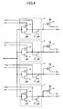
- FIG. 4 shows an example of a circuit configuration of the sub-word circuit 20 .
- the sub-word circuit 20 shown in FIG. 4 includes four sub-word drivers 21 for selectively activating four sub-word lines SWL 0 , SWL 1 , SWL 2 , SWL 3 corresponding to one main word line MWL 0 (not shown in FIG. 4 ), and four precharging PMOS transistors 22 connected to four precharge lines PL 0 to PL 3 .
- Each sub-word driver 21 includes a pair of a PMOS transistor 40 and an NMOS transistor 41 which form an inverter, and includes an NMOS transistor 42 on the output side.
- an inverted main word line MWL 0 B obtained by inverting the main word line MWL 0 is connected to input sides (gates) of the inverters, and sub-word lines SWL 0 to SWL 3 are connected to output sides (drains) of the inverters respectively.
- Sub-word select lines FX 0 , FX 1 , FX 2 and FX 3 are connected to sources of the PMOS transistors 40 respectively, and sources of the NMOS transistors 41 are connected to ground.
- one of the four sub-word select lines FX 0 to FX 3 is selected and becomes a high level, and corresponding one sub-word driver 21 is activated.
- one sub-word line SWL connected to the activated sub-word driver 21 selectively becomes a high level.
- a corresponding precharging PMOS transistor 22 becomes an OFF state, and the precharge line PL on the output side is disconnected from the supply voltage VWL.
- non-selected three of the sub-word select lines FX 0 to FX 3 become a low level, and corresponding three sub-word drivers 21 remain in an inactivated state.
- the NMOS transistor 42 of each sub-word driver 21 is connected between the sub-word line SWL and ground, and inverted sub-word select lines FX 0 B to FX 3 B obtained by inverting the sub-word select lines FX 0 to FX 3 are connected to gates of the NMOS transistors 42 respectively.
- the NMOS transistors 42 are provided for the purpose of avoiding a floating state of the non-selected sub-word lines SWL.
- one precharge line PL 0 corresponding to the selected sub-word line SWL 0 is in a floating state while three precharge lines PL 1 to PL 3 corresponding to the non-selected sub-word lines SWL 1 to SWL 3 become a high level.
- the diffusion layers D connected to the precharge lines PL 1 to PL 3 are precharged through the precharging PMOS transistors 22 , and the potential of the diffusion layers D is pulled up to a high level after a predetermined time elapses.
- the diffusion layer D connected to the precharge line PL 0 is not precharged and becomes a floating state.
- the lower diffusion layer D therebelow is in a state of being charged to a high level, and the lower diode 11 is in a reverse-biased state.
- the connection is made so that the reversed-biased diode 11 is connected between the bit line BL to which the non-selected memory cell MC is connected and the diffusion layer D, thereby the diffusion layer capacitance of the diffusion layer D cannot be seen from the bit line BL.
- the selected memory cell MC since the diffusion layer D is disconnected from the precharge line PL, the lower diode 11 is in a forward-biased state during the operation of the memory cell MC.
- all the diffusion layers D below other non-selected memory cells MC are in a charged state, and therefore it is possible to prevent a decrease in read speed due to the diffusion layer capacitance.
- FIG. 5 times required for precharging the bit line BL are obtained by simulations and compared between the configuration of the embodiment in which the precharging PMOS transistors 22 are provided and the conventional configuration ( FIG. 8 ) without the precharging PMOS transistors 22 .
- the bit line BL is precharged to 1.15V
- a characteristic Ca corresponding to the configuration of the embodiment and a characteristic Cb corresponding to the conventional configuration are shown respectively.
- the voltage changes more rapidly in the configuration of the embodiment than in the conventional configuration, and the effect of precharging the diffusion layers D by the operation of the precharging PMOS transistors 22 can be confirmed.
- the characteristic Ca when assuming that noise not exceeding 10 mV is permitted in precharging the bit line BL, the characteristic Ca requires a time of 2.6 ns while the characteristic Cb requires a time of 5.2 ns. Therefore, the operation speed can be approximately doubled by adopting the embodiment.
- FIG. 1 shows the precharging PMOS transistor 22 functioning as the precharge circuit of the present invention, however the precharge circuit may include an NMOS transistor.
- FIG. 6 shows an example of a circuit configuration of the sub-word circuit 20 in the modification of the embodiment corresponding to the circuit configuration of FIG. 4 .
- the sub-word circuit 20 shown in FIG. 6 includes the four sub-word drivers 21 , and four precharging NMOS transistor 23 connected to the four precharge lines PL 0 to PL 3 .
- the sub-word drivers 21 are configured in the same manner as in FIG. 4 , so description thereof is omitted.
- Each precharging NMOS transistor 23 has a drain connected to the supply voltage VWL, a source connected to the precharge line PL, and a gate connected to the inverted main word line MWL 0 B.
- the inverted main word line MWL 0 B is controlled to be a high level, all the four precharging NMOS transistors 23 become an ON state, and the respective precharge lines PL are connected to the supply voltage VWL. In this manner, the operation in FIG. 6 is the same as that in FIG. 4 during stand-by operation.
- the main word line MWL 0 returns to a non-selected state after this time period elapsed.
- the diffusion layers D are precharged through the precharge lines PL like in the abovementioned stand-by operation. In this manner, even when the circuit configuration of FIG. 6 is employed, it is avoided that the diffusion layers D remain in a floating state in a long period, thereby achieving the same effect as that of the circuit configuration of FIG. 4 .
- the present invention has been specifically described based on the embodiment, the present invention is not limited to the above-described embodiment, and various variations and modifications can be made without departing from the scope of the present invention.
- the circuit configuration of the precharge circuit can be freely selected for the purpose of precharging the diffusion layers D.
- the hierarchical word line structure is employed in order to arrange the main word lines MWL and the sub-word lines SWL in the embodiment, however the present invention can be applied to an arrangement without employing the hierarchical word line structure.
- the layout in which the ground line GL is arranged in a mesh form is employed in the embodiment, however a layout in which the ground line GL extends only in, for example, a bit line direction can be employed.
Abstract
Description
Claims (14)
Applications Claiming Priority (2)
| Application Number | Priority Date | Filing Date | Title |
|---|---|---|---|
| JP2007161936A JP5396011B2 (en) | 2007-06-19 | 2007-06-19 | Phase change memory device |
| JP2007-161936 | 2007-06-19 |
Publications (2)
| Publication Number | Publication Date |
|---|---|
| US20080316806A1 US20080316806A1 (en) | 2008-12-25 |
| US8054679B2 true US8054679B2 (en) | 2011-11-08 |
Family
ID=40136304
Family Applications (1)
| Application Number | Title | Priority Date | Filing Date |
|---|---|---|---|
| US12/213,195 Active 2030-09-08 US8054679B2 (en) | 2007-06-19 | 2008-06-16 | Phase change memory device |
Country Status (4)
| Country | Link |
|---|---|
| US (1) | US8054679B2 (en) |
| JP (1) | JP5396011B2 (en) |
| CN (1) | CN101329910B (en) |
| TW (1) | TW200901216A (en) |
Cited By (34)
| Publication number | Priority date | Publication date | Assignee | Title |
|---|---|---|---|---|
| US20100184803A1 (en) * | 2007-03-09 | 2010-07-22 | Link Medicine Corporation | Treatment of Lysosomal Storage Diseases |
| US20100232208A1 (en) * | 2009-03-16 | 2010-09-16 | Kabushiki Kaisha Toshiba | Method of executing a forming operation to variable resistance element |
| US20130027081A1 (en) * | 2011-07-29 | 2013-01-31 | Crossbar, Inc. | Field programmable gate array utilizing two-terminal non-volatile memory |
| US20130033923A1 (en) * | 2010-10-07 | 2013-02-07 | Crossbar, Inc. | Circuit for concurrent read operation and method therefor |
| US8619459B1 (en) | 2011-06-23 | 2013-12-31 | Crossbar, Inc. | High operating speed resistive random access memory |
| US8754671B2 (en) | 2011-07-29 | 2014-06-17 | Crossbar, Inc. | Field programmable gate array utilizing two-terminal non-volatile memory |
| US20140268997A1 (en) * | 2013-03-15 | 2014-09-18 | Crossbar, Inc. | Programming two-terminal memory cells with reduced program current |
| US8988927B2 (en) | 2010-06-14 | 2015-03-24 | Crossbar, Inc. | Non-volatile variable capacitive device including resistive memory cell |
| US9001552B1 (en) | 2012-06-22 | 2015-04-07 | Crossbar, Inc. | Programming a RRAM method and apparatus |
| US9013911B2 (en) | 2011-06-23 | 2015-04-21 | Crossbar, Inc. | Memory array architecture with two-terminal memory cells |
| US9059705B1 (en) | 2011-06-30 | 2015-06-16 | Crossbar, Inc. | Resistive random accessed memory device for FPGA configuration |
| US9058865B1 (en) | 2011-06-30 | 2015-06-16 | Crossbar, Inc. | Multi-level cell operation in silver/amorphous silicon RRAM |
| US9543359B2 (en) | 2011-05-31 | 2017-01-10 | Crossbar, Inc. | Switching device having a non-linear element |
| US9564587B1 (en) | 2011-06-30 | 2017-02-07 | Crossbar, Inc. | Three-dimensional two-terminal memory with enhanced electric field and segmented interconnects |
| US9570678B1 (en) | 2010-06-08 | 2017-02-14 | Crossbar, Inc. | Resistive RAM with preferental filament formation region and methods |
| US9576616B2 (en) | 2012-10-10 | 2017-02-21 | Crossbar, Inc. | Non-volatile memory with overwrite capability and low write amplification |
| US9583701B1 (en) | 2012-08-14 | 2017-02-28 | Crossbar, Inc. | Methods for fabricating resistive memory device switching material using ion implantation |
| USRE46335E1 (en) | 2010-11-04 | 2017-03-07 | Crossbar, Inc. | Switching device having a non-linear element |
| US9590013B2 (en) | 2010-08-23 | 2017-03-07 | Crossbar, Inc. | Device switching using layered device structure |
| US9601690B1 (en) | 2011-06-30 | 2017-03-21 | Crossbar, Inc. | Sub-oxide interface layer for two-terminal memory |
| US9601692B1 (en) | 2010-07-13 | 2017-03-21 | Crossbar, Inc. | Hetero-switching layer in a RRAM device and method |
| US9620206B2 (en) | 2011-05-31 | 2017-04-11 | Crossbar, Inc. | Memory array architecture with two-terminal memory cells |
| US9627443B2 (en) | 2011-06-30 | 2017-04-18 | Crossbar, Inc. | Three-dimensional oblique two-terminal memory with enhanced electric field |
| US9673255B2 (en) | 2012-04-05 | 2017-06-06 | Crossbar, Inc. | Resistive memory device and fabrication methods |
| US9685608B2 (en) | 2012-04-13 | 2017-06-20 | Crossbar, Inc. | Reduced diffusion in metal electrode for two-terminal memory |
| US9729155B2 (en) | 2011-07-29 | 2017-08-08 | Crossbar, Inc. | Field programmable gate array utilizing two-terminal non-volatile memory |
| US9735358B2 (en) | 2012-08-14 | 2017-08-15 | Crossbar, Inc. | Noble metal / non-noble metal electrode for RRAM applications |
| US9741765B1 (en) | 2012-08-14 | 2017-08-22 | Crossbar, Inc. | Monolithically integrated resistive memory using integrated-circuit foundry compatible processes |
| US9793474B2 (en) | 2012-04-20 | 2017-10-17 | Crossbar, Inc. | Low temperature P+ polycrystalline silicon material for non-volatile memory device |
| US9972778B2 (en) | 2012-05-02 | 2018-05-15 | Crossbar, Inc. | Guided path for forming a conductive filament in RRAM |
| US10056907B1 (en) | 2011-07-29 | 2018-08-21 | Crossbar, Inc. | Field programmable gate array utilizing two-terminal non-volatile memory |
| US10096362B1 (en) | 2017-03-24 | 2018-10-09 | Crossbar, Inc. | Switching block configuration bit comprising a non-volatile memory cell |
| US10290801B2 (en) | 2014-02-07 | 2019-05-14 | Crossbar, Inc. | Scalable silicon based resistive memory device |
| US11107524B2 (en) | 2019-07-29 | 2021-08-31 | Samsung Electronics Co., Ltd. | Methods and apparatus for resisitive memory device for sense margin compensation |
Families Citing this family (3)
| Publication number | Priority date | Publication date | Assignee | Title |
|---|---|---|---|---|
| KR100900135B1 (en) * | 2007-12-21 | 2009-06-01 | 주식회사 하이닉스반도체 | Phase change memory device |
| JP2011192333A (en) | 2010-03-12 | 2011-09-29 | Elpida Memory Inc | Semiconductor device |
| CN103871463B (en) * | 2014-03-26 | 2017-02-08 | 中国科学院上海微系统与信息技术研究所 | Phase change memory array stacked structure and operating method thereof |
Citations (3)
| Publication number | Priority date | Publication date | Assignee | Title |
|---|---|---|---|---|
| US20050270883A1 (en) | 2004-06-08 | 2005-12-08 | Beak-Hyung Cho | Memory device with reduced word line resistance |
| US20060097343A1 (en) * | 2004-11-08 | 2006-05-11 | Ward Parkinson | Programmable matrix array with phase-change material |
| US20060097240A1 (en) * | 2004-11-08 | 2006-05-11 | Tyler Lowrey | Programmable matrix array with chalcogenide material |
Family Cites Families (6)
| Publication number | Priority date | Publication date | Assignee | Title |
|---|---|---|---|---|
| AU2002331580A1 (en) * | 2002-08-14 | 2004-03-03 | Intel Corporation | Method for reading a structural phase-change memory |
| KR101010175B1 (en) * | 2004-04-23 | 2011-01-20 | 주식회사 하이닉스반도체 | Sense amp and phase change memory using the sense amp |
| JP4606869B2 (en) * | 2004-12-24 | 2011-01-05 | ルネサスエレクトロニクス株式会社 | Semiconductor device |
| KR100735525B1 (en) * | 2006-01-04 | 2007-07-04 | 삼성전자주식회사 | Phase change memory device |
| JP2008277543A (en) * | 2007-04-27 | 2008-11-13 | Toshiba Corp | Nonvolatile semiconductor memory device |
| US7684227B2 (en) * | 2007-05-31 | 2010-03-23 | Micron Technology, Inc. | Resistive memory architectures with multiple memory cells per access device |
-
2007
- 2007-06-19 JP JP2007161936A patent/JP5396011B2/en not_active Expired - Fee Related
-
2008
- 2008-05-29 TW TW097119856A patent/TW200901216A/en unknown
- 2008-06-12 CN CN2008101094532A patent/CN101329910B/en not_active Expired - Fee Related
- 2008-06-16 US US12/213,195 patent/US8054679B2/en active Active
Patent Citations (7)
| Publication number | Priority date | Publication date | Assignee | Title |
|---|---|---|---|---|
| US20050270883A1 (en) | 2004-06-08 | 2005-12-08 | Beak-Hyung Cho | Memory device with reduced word line resistance |
| US20060097343A1 (en) * | 2004-11-08 | 2006-05-11 | Ward Parkinson | Programmable matrix array with phase-change material |
| US20060097240A1 (en) * | 2004-11-08 | 2006-05-11 | Tyler Lowrey | Programmable matrix array with chalcogenide material |
| US7365355B2 (en) * | 2004-11-08 | 2008-04-29 | Ovonyx, Inc. | Programmable matrix array with phase-change material |
| US20080211539A1 (en) * | 2004-11-08 | 2008-09-04 | Ward Parkinson | Programmable matrix array with phase-change material |
| US7646630B2 (en) * | 2004-11-08 | 2010-01-12 | Ovonyx, Inc. | Programmable matrix array with chalcogenide material |
| US7706178B2 (en) * | 2004-11-08 | 2010-04-27 | Ovonyx, Inc. | Programmable matrix array with phase-change material |
Cited By (45)
| Publication number | Priority date | Publication date | Assignee | Title |
|---|---|---|---|---|
| US20100184803A1 (en) * | 2007-03-09 | 2010-07-22 | Link Medicine Corporation | Treatment of Lysosomal Storage Diseases |
| US20100232208A1 (en) * | 2009-03-16 | 2010-09-16 | Kabushiki Kaisha Toshiba | Method of executing a forming operation to variable resistance element |
| US8391047B2 (en) * | 2009-03-16 | 2013-03-05 | Kabushiki Kaisha Toshiba | Method of executing a forming operation to variable resistance element |
| US9570678B1 (en) | 2010-06-08 | 2017-02-14 | Crossbar, Inc. | Resistive RAM with preferental filament formation region and methods |
| US8988927B2 (en) | 2010-06-14 | 2015-03-24 | Crossbar, Inc. | Non-volatile variable capacitive device including resistive memory cell |
| US9601692B1 (en) | 2010-07-13 | 2017-03-21 | Crossbar, Inc. | Hetero-switching layer in a RRAM device and method |
| US9590013B2 (en) | 2010-08-23 | 2017-03-07 | Crossbar, Inc. | Device switching using layered device structure |
| US10224370B2 (en) | 2010-08-23 | 2019-03-05 | Crossbar, Inc. | Device switching using layered device structure |
| US8675384B2 (en) * | 2010-10-07 | 2014-03-18 | Crossbar, Inc. | Circuit for concurrent read operation and method therefor |
| US20130033923A1 (en) * | 2010-10-07 | 2013-02-07 | Crossbar, Inc. | Circuit for concurrent read operation and method therefor |
| US9047939B2 (en) | 2010-10-07 | 2015-06-02 | Crossbar, Inc. | Circuit for concurrent read operation and method therefor |
| USRE46335E1 (en) | 2010-11-04 | 2017-03-07 | Crossbar, Inc. | Switching device having a non-linear element |
| US9620206B2 (en) | 2011-05-31 | 2017-04-11 | Crossbar, Inc. | Memory array architecture with two-terminal memory cells |
| US9543359B2 (en) | 2011-05-31 | 2017-01-10 | Crossbar, Inc. | Switching device having a non-linear element |
| US8619459B1 (en) | 2011-06-23 | 2013-12-31 | Crossbar, Inc. | High operating speed resistive random access memory |
| US9013911B2 (en) | 2011-06-23 | 2015-04-21 | Crossbar, Inc. | Memory array architecture with two-terminal memory cells |
| US9633723B2 (en) | 2011-06-23 | 2017-04-25 | Crossbar, Inc. | High operating speed resistive random access memory |
| US9058865B1 (en) | 2011-06-30 | 2015-06-16 | Crossbar, Inc. | Multi-level cell operation in silver/amorphous silicon RRAM |
| US9601690B1 (en) | 2011-06-30 | 2017-03-21 | Crossbar, Inc. | Sub-oxide interface layer for two-terminal memory |
| US9627443B2 (en) | 2011-06-30 | 2017-04-18 | Crossbar, Inc. | Three-dimensional oblique two-terminal memory with enhanced electric field |
| US9570683B1 (en) | 2011-06-30 | 2017-02-14 | Crossbar, Inc. | Three-dimensional two-terminal memory with enhanced electric field and segmented interconnects |
| US9059705B1 (en) | 2011-06-30 | 2015-06-16 | Crossbar, Inc. | Resistive random accessed memory device for FPGA configuration |
| US9564587B1 (en) | 2011-06-30 | 2017-02-07 | Crossbar, Inc. | Three-dimensional two-terminal memory with enhanced electric field and segmented interconnects |
| US8754671B2 (en) | 2011-07-29 | 2014-06-17 | Crossbar, Inc. | Field programmable gate array utilizing two-terminal non-volatile memory |
| US9054702B2 (en) | 2011-07-29 | 2015-06-09 | Crossbar, Inc. | Field programmable gate array utilizing two-terminal non-volatile memory |
| US10056907B1 (en) | 2011-07-29 | 2018-08-21 | Crossbar, Inc. | Field programmable gate array utilizing two-terminal non-volatile memory |
| US8674724B2 (en) * | 2011-07-29 | 2014-03-18 | Crossbar, Inc. | Field programmable gate array utilizing two-terminal non-volatile memory |
| US20130027081A1 (en) * | 2011-07-29 | 2013-01-31 | Crossbar, Inc. | Field programmable gate array utilizing two-terminal non-volatile memory |
| US9729155B2 (en) | 2011-07-29 | 2017-08-08 | Crossbar, Inc. | Field programmable gate array utilizing two-terminal non-volatile memory |
| US9673255B2 (en) | 2012-04-05 | 2017-06-06 | Crossbar, Inc. | Resistive memory device and fabrication methods |
| US10910561B1 (en) | 2012-04-13 | 2021-02-02 | Crossbar, Inc. | Reduced diffusion in metal electrode for two-terminal memory |
| US9685608B2 (en) | 2012-04-13 | 2017-06-20 | Crossbar, Inc. | Reduced diffusion in metal electrode for two-terminal memory |
| US9793474B2 (en) | 2012-04-20 | 2017-10-17 | Crossbar, Inc. | Low temperature P+ polycrystalline silicon material for non-volatile memory device |
| US9972778B2 (en) | 2012-05-02 | 2018-05-15 | Crossbar, Inc. | Guided path for forming a conductive filament in RRAM |
| US9001552B1 (en) | 2012-06-22 | 2015-04-07 | Crossbar, Inc. | Programming a RRAM method and apparatus |
| US9741765B1 (en) | 2012-08-14 | 2017-08-22 | Crossbar, Inc. | Monolithically integrated resistive memory using integrated-circuit foundry compatible processes |
| US9735358B2 (en) | 2012-08-14 | 2017-08-15 | Crossbar, Inc. | Noble metal / non-noble metal electrode for RRAM applications |
| US9583701B1 (en) | 2012-08-14 | 2017-02-28 | Crossbar, Inc. | Methods for fabricating resistive memory device switching material using ion implantation |
| US10096653B2 (en) | 2012-08-14 | 2018-10-09 | Crossbar, Inc. | Monolithically integrated resistive memory using integrated-circuit foundry compatible processes |
| US9576616B2 (en) | 2012-10-10 | 2017-02-21 | Crossbar, Inc. | Non-volatile memory with overwrite capability and low write amplification |
| US9627057B2 (en) * | 2013-03-15 | 2017-04-18 | Crossbar, Inc. | Programming two-terminal memory cells with reduced program current |
| US20140268997A1 (en) * | 2013-03-15 | 2014-09-18 | Crossbar, Inc. | Programming two-terminal memory cells with reduced program current |
| US10290801B2 (en) | 2014-02-07 | 2019-05-14 | Crossbar, Inc. | Scalable silicon based resistive memory device |
| US10096362B1 (en) | 2017-03-24 | 2018-10-09 | Crossbar, Inc. | Switching block configuration bit comprising a non-volatile memory cell |
| US11107524B2 (en) | 2019-07-29 | 2021-08-31 | Samsung Electronics Co., Ltd. | Methods and apparatus for resisitive memory device for sense margin compensation |
Also Published As
| Publication number | Publication date |
|---|---|
| CN101329910B (en) | 2012-06-13 |
| CN101329910A (en) | 2008-12-24 |
| JP2009004000A (en) | 2009-01-08 |
| US20080316806A1 (en) | 2008-12-25 |
| JP5396011B2 (en) | 2014-01-22 |
| TW200901216A (en) | 2009-01-01 |
Similar Documents
| Publication | Publication Date | Title |
|---|---|---|
| US8054679B2 (en) | Phase change memory device | |
| US7719870B2 (en) | Storage device | |
| US7903448B2 (en) | Resistance random access memory having common source line | |
| US7843715B2 (en) | Memory cell of a resistive semiconductor memory device, a resistive semiconductor memory device having a three-dimensional stack structure, and related methods | |
| US8107275B2 (en) | Nonvolatile memory device using variable resistive element | |
| KR101115756B1 (en) | Highly integrated programmable non-volatile memory and the manufacturing method thereof | |
| EP1560221A2 (en) | Semiconductor memory device | |
| US7957180B2 (en) | Phase change memory device having decentralized driving units | |
| JP2007164925A (en) | Nonvolatile semiconductor memory device | |
| KR20020023109A (en) | Magnetic thin-film memory device for quick and stable reading | |
| CN111816238B (en) | Resistive memory device | |
| US7944739B2 (en) | Phase change memory device with bit line discharge path | |
| CN101174646A (en) | Semiconductor memory device and layout structure of word line contacts | |
| US9013917B2 (en) | Semiconductor memory device | |
| US8310874B2 (en) | Non-volatile memory device | |
| JP6137180B2 (en) | Programming circuit, semiconductor device, and programming method | |
| KR101051166B1 (en) | Phase change memory device | |
| JP2012195038A (en) | Semiconductor storage device | |
| JP2011192333A (en) | Semiconductor device | |
| US8358533B2 (en) | Phase-change memory device | |
| CN115331712A (en) | Variable resistance memory device, memory system including the same, and method of driving the same | |
| KR20130015925A (en) | Semiconductor memory device |
Legal Events
| Date | Code | Title | Description |
|---|---|---|---|
| AS | Assignment |
Owner name: ELPIDA MEMORY INC., JAPAN Free format text: ASSIGNMENT OF ASSIGNORS INTEREST;ASSIGNORS:NAKAI, KIYOSHI;TSUKADA, SHUICHI;JONO, YUSUKE;REEL/FRAME:021159/0859 Effective date: 20080528 |
|
| STCF | Information on status: patent grant |
Free format text: PATENTED CASE |
|
| AS | Assignment |
Owner name: ELPIDA MEMORY INC., JAPAN Free format text: SECURITY AGREEMENT;ASSIGNOR:PS4 LUXCO S.A.R.L.;REEL/FRAME:032414/0261 Effective date: 20130726 |
|
| AS | Assignment |
Owner name: PS4 LUXCO S.A.R.L., LUXEMBOURG Free format text: ASSIGNMENT OF ASSIGNORS INTEREST;ASSIGNOR:ELPIDA MEMORY, INC.;REEL/FRAME:032899/0588 Effective date: 20130726 |
|
| FEPP | Fee payment procedure |
Free format text: PAYOR NUMBER ASSIGNED (ORIGINAL EVENT CODE: ASPN); ENTITY STATUS OF PATENT OWNER: LARGE ENTITY |
|
| FPAY | Fee payment |
Year of fee payment: 4 |
|
| AS | Assignment |
Owner name: PS5 LUXCO S.A.R.L., LUXEMBOURG Free format text: ASSIGNMENT OF ASSIGNORS INTEREST;ASSIGNOR:PS4 LUXCO S.A.R.L.;REEL/FRAME:039818/0506 Effective date: 20130829 Owner name: LONGITUDE SEMICONDUCTOR S.A.R.L., LUXEMBOURG Free format text: CHANGE OF NAME;ASSIGNOR:PS5 LUXCO S.A.R.L.;REEL/FRAME:039793/0880 Effective date: 20131112 |
|
| AS | Assignment |
Owner name: LONGITUDE LICENSING LIMITED, IRELAND Free format text: ASSIGNMENT OF ASSIGNORS INTEREST;ASSIGNOR:LONGITUDE SEMICONDUCTOR S.A.R.L.;REEL/FRAME:046867/0248 Effective date: 20180731 |
|
| MAFP | Maintenance fee payment |
Free format text: PAYMENT OF MAINTENANCE FEE, 8TH YEAR, LARGE ENTITY (ORIGINAL EVENT CODE: M1552); ENTITY STATUS OF PATENT OWNER: LARGE ENTITY Year of fee payment: 8 |
|
| MAFP | Maintenance fee payment |
Free format text: PAYMENT OF MAINTENANCE FEE, 12TH YEAR, LARGE ENTITY (ORIGINAL EVENT CODE: M1553); ENTITY STATUS OF PATENT OWNER: LARGE ENTITY Year of fee payment: 12 |