JP4606869B2 - Semiconductor device - Google Patents
Semiconductor device Download PDFInfo
- Publication number
- JP4606869B2 JP4606869B2 JP2004374314A JP2004374314A JP4606869B2 JP 4606869 B2 JP4606869 B2 JP 4606869B2 JP 2004374314 A JP2004374314 A JP 2004374314A JP 2004374314 A JP2004374314 A JP 2004374314A JP 4606869 B2 JP4606869 B2 JP 4606869B2
- Authority
- JP
- Japan
- Prior art keywords
- bit line
- semiconductor device
- potential
- sense amplifier
- switch
- Prior art date
- Legal status (The legal status is an assumption and is not a legal conclusion. Google has not performed a legal analysis and makes no representation as to the accuracy of the status listed.)
- Expired - Fee Related
Links
Images


Classifications
-
- G—PHYSICS
- G11—INFORMATION STORAGE
- G11C—STATIC STORES
- G11C13/00—Digital stores characterised by the use of storage elements not covered by groups G11C11/00, G11C23/00, or G11C25/00
- G11C13/0002—Digital stores characterised by the use of storage elements not covered by groups G11C11/00, G11C23/00, or G11C25/00 using resistive RAM [RRAM] elements
- G11C13/0004—Digital stores characterised by the use of storage elements not covered by groups G11C11/00, G11C23/00, or G11C25/00 using resistive RAM [RRAM] elements comprising amorphous/crystalline phase transition cells
-
- G—PHYSICS
- G11—INFORMATION STORAGE
- G11C—STATIC STORES
- G11C13/00—Digital stores characterised by the use of storage elements not covered by groups G11C11/00, G11C23/00, or G11C25/00
- G11C13/0002—Digital stores characterised by the use of storage elements not covered by groups G11C11/00, G11C23/00, or G11C25/00 using resistive RAM [RRAM] elements
- G11C13/0021—Auxiliary circuits
- G11C13/0023—Address circuits or decoders
- G11C13/0026—Bit-line or column circuits
-
- G—PHYSICS
- G11—INFORMATION STORAGE
- G11C—STATIC STORES
- G11C13/00—Digital stores characterised by the use of storage elements not covered by groups G11C11/00, G11C23/00, or G11C25/00
- G11C13/0002—Digital stores characterised by the use of storage elements not covered by groups G11C11/00, G11C23/00, or G11C25/00 using resistive RAM [RRAM] elements
- G11C13/0021—Auxiliary circuits
- G11C13/004—Reading or sensing circuits or methods
-
- G—PHYSICS
- G11—INFORMATION STORAGE
- G11C—STATIC STORES
- G11C7/00—Arrangements for writing information into, or reading information out from, a digital store
- G11C7/12—Bit line control circuits, e.g. drivers, boosters, pull-up circuits, pull-down circuits, precharging circuits, equalising circuits, for bit lines
-
- G—PHYSICS
- G11—INFORMATION STORAGE
- G11C—STATIC STORES
- G11C13/00—Digital stores characterised by the use of storage elements not covered by groups G11C11/00, G11C23/00, or G11C25/00
- G11C13/0002—Digital stores characterised by the use of storage elements not covered by groups G11C11/00, G11C23/00, or G11C25/00 using resistive RAM [RRAM] elements
- G11C13/0021—Auxiliary circuits
- G11C13/004—Reading or sensing circuits or methods
- G11C2013/0054—Read is performed on a reference element, e.g. cell, and the reference sensed value is used to compare the sensed value of the selected cell
-
- G—PHYSICS
- G11—INFORMATION STORAGE
- G11C—STATIC STORES
- G11C13/00—Digital stores characterised by the use of storage elements not covered by groups G11C11/00, G11C23/00, or G11C25/00
- G11C13/0002—Digital stores characterised by the use of storage elements not covered by groups G11C11/00, G11C23/00, or G11C25/00 using resistive RAM [RRAM] elements
- G11C13/0021—Auxiliary circuits
- G11C13/004—Reading or sensing circuits or methods
- G11C2013/0057—Read done in two steps, e.g. wherein the cell is read twice and one of the two read values serving as a reference value
Description
本発明は、半導体装置に関し、特に相変化材料を用いて形成される、高密度集積メモリ回路、あるいはメモリ回路と論理回路とが同一半導体基板に設けられたロジック混載型メモリ、あるいはアナログ回路を有する半導体装置に適用して有効な技術に関するものである。 The present invention relates to a semiconductor device, in particular, a high-density integrated memory circuit formed using a phase change material, or a logic-embedded memory in which a memory circuit and a logic circuit are provided on the same semiconductor substrate, or an analog circuit. The present invention relates to a technique effective when applied to a semiconductor device.
本発明者が検討したところによれば、相変化材料を用いたメモリの技術に関しては、以下のようなものが考えられる。 According to a study by the present inventor, the following can be considered as a memory technology using a phase change material.
高速で高集積な不揮発性メモリを目指して、相変化メモリの開発が進められている。相変化材料からなる抵抗素子を用いたメモリ(相変化メモリ)は、電気パルスを用いて、図31のような温度変化を起こさせて相変化材料を非晶質状態と結晶状態間で相転移させ、図32にあるように、非晶質状態(リセット)と結晶状態(セット)の抵抗値の違いを情報として記録する不揮発メモリである。なお、相変化材料の非晶質状態の高抵抗値および結晶状態の低抵抗値は、それぞれ、完全な非晶質状態および完全な結晶状態である必要はなく、記憶素子としては、高抵抗状態と低抵抗状態に十分な抵抗差があることが重要であり、完全な非晶質状態である高抵抗状態と完全な結晶状態である低抵抗状態の中間の任意の値をとることが可能である。 Phase change memory is being developed with the aim of high-speed and highly integrated nonvolatile memory. A memory using a resistance element made of a phase change material (phase change memory) uses an electric pulse to cause a temperature change as shown in FIG. 31 to cause phase transition of the phase change material between an amorphous state and a crystalline state. As shown in FIG. 32, the non-volatile memory records the difference in resistance value between the amorphous state (reset) and the crystalline state (set) as information. Note that the high resistance value in the amorphous state and the low resistance value in the crystalline state of the phase change material do not need to be in a completely amorphous state and a complete crystalline state, respectively. It is important that there is a sufficient resistance difference between the low resistance state and any value between the high resistance state, which is a completely amorphous state, and the low resistance state, which is a completely crystalline state. is there.
相変化素子は、前述のように、電気パルスによってその相状態を変える。リセットするためには、短い期間大電流を流し、急速に冷却することが必要である。逆に、セットするためには、リセット時よりも少ない電流を、比較的長時間流し、ゆっくり冷却することが必要である。一方、読み出し動作では、書換え電圧に比べて十分低い読み出し電圧を用いてビット線の電圧降下の速度をセンスすることにより、相変化メモリの‘0’状態および‘1’状態を読み出す。 As described above, the phase change element changes its phase state by an electric pulse. In order to reset, it is necessary to flow a large current for a short period of time and to cool rapidly. On the other hand, in order to set, it is necessary to flow a current smaller than that at the time of resetting for a relatively long time and cool slowly. On the other hand, in the read operation, the ‘0’ state and the ‘1’ state of the phase change memory are read by sensing the speed of the voltage drop of the bit line using a read voltage sufficiently lower than the rewrite voltage.
相変化メモリの読み出し方式として、例えば、非特許文献1には、電荷転送型のプリアンプを用いてセンスアンプへの入力信号を増幅し、センスアンプリファレンスレベルを容易に設定することを可能にする技術が示されている。
ところで、前記のような相変化材料を用いたメモリの技術について、本発明者が検討した結果、以下のようなことが明らかとなった。 By the way, as a result of the study of the memory technology using the phase change material as described above, the following has been clarified.
相変化メモリでは、読み出し動作も書換え動作も素子に電流を流す。書換え動作では、抵抗自身あるいは、隣接して配置されるヒーターに大電流を流すことにより生じるジュール熱によって、素子の相状態、例えば、アモルファス状態(高抵抗状態)と結晶状態(低抵抗状態)を変える。 In the phase change memory, a current is passed through the element in both the read operation and the rewrite operation. In the rewriting operation, the phase state of the element, for example, the amorphous state (high resistance state) and the crystalline state (low resistance state) are caused by Joule heat generated by flowing a large current through the resistor itself or a heater arranged adjacently. Change.
一方、読み出し動作では、素子、あるいは隣接するヒーターに電流が流れるため、その電流で発生するジュール熱によって、当該素子のデータが破壊される恐れがある。また、読み出し電流を流した際に、内部電圧の揺らぎ、外部温度、素子バラツキなどの影響で、予想以上の熱ディスターブが発生し、周辺のメモリ素子の記憶データが破壊される可能性も考えられる。このようなことから、読み出し時の印加電圧を可能な限り小さくすることで、素子及びヒーターに流れる電流を低減し、発熱量を小さくすることが課題となる。 On the other hand, in the read operation, since a current flows through the element or an adjacent heater, the data of the element may be destroyed by Joule heat generated by the current. In addition, when a read current is applied, there is a possibility that the thermal disturbance more than expected due to fluctuations in internal voltage, external temperature, element variation, etc., and the stored data in the peripheral memory elements may be destroyed. . For this reason, it becomes a problem to reduce the amount of heat generated by reducing the current flowing through the element and the heater by reducing the applied voltage at the time of reading as much as possible.
低抵抗状態と高抵抗状態を感知する方法として、素子に一定の電圧を印加して、素子に流れる電流を参照電流と比較して感知する電流センス方式と、メモリ素子を介して容量性の負荷を充電あるいは放電し、一定時間後の電圧値を参照電圧と比較して感知する電圧センス方式がある。電流センス方式は、センス回路の規模が大きくなるため、一度に多ビットを読み出す動作には、電圧センスの方が好適である。しかしながら、電圧センス方式では、読み出し時の印加電圧が小さいと参照電圧と読み出し電圧の差が小さくなるため、安定した参照電圧を作り出すことが課題となる。 As a method of sensing the low resistance state and the high resistance state, a current sensing method in which a constant voltage is applied to the element and the current flowing through the element is compared with a reference current, and a capacitive load is provided via the memory element. There is a voltage sensing method in which a voltage value after a certain time is sensed by comparing with a reference voltage. In the current sensing method, since the scale of the sensing circuit is increased, voltage sensing is more suitable for the operation of reading multiple bits at a time. However, in the voltage sensing method, if the applied voltage at the time of reading is small, the difference between the reference voltage and the reading voltage becomes small, so that it becomes a problem to create a stable reference voltage.
このような中、例えば、前述した非特許文献1には、電荷転送型のプリアンプを用いる方式が示されている。しかしながら、非特許文献1に記載される方式では、電荷転送アンプを構成するパスゲートトランジスタのゲート電圧をうまく調節しなければ、プリアンプとして動作しないため、センスアンプ入力信号振幅を大きくすることができない恐れがある。 Under such circumstances, for example, Non-Patent Document 1 described above discloses a method using a charge transfer type preamplifier. However, in the method described in Non-Patent Document 1, since it does not operate as a preamplifier unless the gate voltage of the pass gate transistor constituting the charge transfer amplifier is adjusted well, there is a risk that the sense amplifier input signal amplitude cannot be increased. There is.
本願において開示される発明のうち、代表的なものの概要を簡単に説明すれば、次のとおりである。 Of the inventions disclosed in the present application, the outline of typical ones will be briefly described as follows.
本発明の半導体装置は、複数のワード線、第1ビット線およびセンスアンプと、複数のワード線と第1ビット線の任意の交点に配置される複数のメモリセルと、センスアンプに接続される第2ビット線および第3ビット線と、第1ビット線に第1電位を与える第1スイッチと、第2ビット線に第2電位を与える第2スイッチと、第1ビット線と第2ビット線を接続する第3スイッチとを備えており、第1スイッチを非活性化した後、複数のワード線のいずれかを活性化し、第3スイッチを活性化する動作を有するものとなっている。 The semiconductor device of the present invention is connected to a plurality of word lines, a first bit line and a sense amplifier, a plurality of memory cells arranged at arbitrary intersections of the plurality of word lines and the first bit line, and the sense amplifier. Second bit line and third bit line; first switch for applying first potential to first bit line; second switch for applying second potential to second bit line; first bit line and second bit line And a third switch for connecting the first and second switches. After the first switch is deactivated, one of the plurality of word lines is activated to activate the third switch.
すなわち、読み出し動作において、まず、メモリセルが接続される第1ビット線に対して予め第1電位をプリチャージした状態で、当該メモリセルのワード線を立ち上げることでメモリセルを介して第1ビット線の電荷を充放電する。その後、第1ビット線と、予め第2電位にプリチャージされ、かつセンスアンプの一方の入力ノードに接続された第2ビット線とを接続することで、メモリセルを介して第1ビット線を再度充放電すると共に第1ビット線と等電位となる第2ビット線からセンスアンプの入力信号を得る。 That is, in the read operation, first, the first potential is precharged with respect to the first bit line to which the memory cell is connected, and the first word line of the memory cell is raised to start the first through the memory cell. Charges / discharges the bit line charge. Thereafter, the first bit line is connected to the second bit line that is precharged to the second potential and connected to one input node of the sense amplifier, thereby connecting the first bit line via the memory cell. The input signal of the sense amplifier is obtained from the second bit line which is charged / discharged again and has the same potential as the first bit line.
このように、センスアンプの入力信号として所望の電圧振幅を得る際に、段階的な充放電を用いることで、1回の充放電に伴う電荷量を減らし、この電荷量に伴う電流または電圧を減らすことで、メモリセルの発熱を抑えることが可能となる。これによって、信頼性が高い読み出し動作が可能となる。 In this way, when obtaining a desired voltage amplitude as an input signal of the sense amplifier, by using stepwise charging / discharging, the amount of charge accompanying one charge / discharge is reduced, and the current or voltage associated with this amount of charge is reduced. By reducing, it becomes possible to suppress the heat generation of the memory cell. This enables a highly reliable read operation.
また、前述したセンスアンプの他方の入力ノードには、リファレンスとして第3ビット線が接続され、このビット線への入力信号は、例えば、内部電源降圧回路などを用いて固定電圧となる第3電位を生成してもよいし、第1のビット線に平行して配置され、読み出し時に非選択となる第4ビット線などを用いてもよい。 Also, a third bit line is connected as a reference to the other input node of the sense amplifier described above, and an input signal to this bit line is, for example, a third potential that becomes a fixed voltage using an internal power supply step-down circuit or the like. Or a fourth bit line that is arranged in parallel with the first bit line and is not selected at the time of reading may be used.
後者の場合、例えば、第3ビット線が第2ビット線と同様に第1電位よりも高い第2電位にプリチャージされ、かつ第4ビット線が非選択のため第1電位よりも低い第4電位にプリチャージされた状態で、第3ビット線と第4ビット線を接続する。これによって、第2ビット線に読み出される‘H’レベル信号と‘L’レベル信号のほぼ中間レベルの信号を、リファレンスとして第3ビット線に供給することが可能となる。この際に、第2ビット線への信号読み出しと同様の機構で第3ビット線に参照電圧を発生させるため、電圧変動または製造ばらつき等に伴うノイズ耐性が高く、安定した参照電圧を生成することが可能となる。 In the latter case, for example, the third bit line is precharged to a second potential higher than the first potential similarly to the second bit line, and the fourth bit line is lower than the first potential because the fourth bit line is not selected. The third bit line and the fourth bit line are connected in a state precharged to the potential. As a result, it is possible to supply a substantially intermediate level signal between the ‘H’ level signal and the ‘L’ level signal read to the second bit line to the third bit line as a reference. At this time, since the reference voltage is generated on the third bit line by the same mechanism as the signal reading to the second bit line, a stable reference voltage having high noise resistance due to voltage fluctuation or manufacturing variation is generated. Is possible.
また、非選択となる第4ビット線を第4電位とするのは、待機時等のメモリセルへの読み書きが不要な間、第4ビット線に接続されたメモリセルへの電圧印加を抑えるためでもある。従って、第4ビット線に限らず、メモリセルに接続されるビット線は、読み書き等で電圧印加が必要な時以外は、スイッチを用いて第4電位に設定しておく。 The fourth bit line that is not selected is set to the fourth potential in order to suppress voltage application to the memory cell connected to the fourth bit line while reading / writing to the memory cell is not required during standby or the like. But there is. Accordingly, not only the fourth bit line but also the bit line connected to the memory cell is set to the fourth potential using a switch except when voltage application is required for reading and writing.
なお、前述したような効果は、メモリセルの記憶素子がカルコゲナイド材料などの可変抵抗素子である場合に特に有益なものとなる。 Note that the above-described effects are particularly beneficial when the memory element of the memory cell is a variable resistance element such as a chalcogenide material.
本願において開示される発明のうち、代表的なものによって得られる効果を簡単に説明すれば、特に相変化材料を含む半導体装置において、読み出し動作の信頼性が向上し、また、安定した参照電圧の発生が実現可能となる。 The effects obtained by typical ones of the inventions disclosed in this application will be briefly described. In particular, in a semiconductor device including a phase change material, reliability of a read operation is improved, and a stable reference voltage is obtained. Occurrence can be realized.
以下、本発明の実施の形態を図面に基づいて詳細に説明する。なお、実施の形態を説明するための全図において、同一の部材には原則として同一の符号を付し、その繰り返しの説明は省略する。また、実施の形態の各機能ブロックを構成する回路素子は、特に制限されないが、公知のCMOS(相補型MOSトランジスタ)等の集積回路技術によって、単結晶シリコンのような半導体基板上に形成される。 Hereinafter, embodiments of the present invention will be described in detail with reference to the drawings. Note that components having the same function are denoted by the same reference symbols throughout the drawings for describing the embodiment, and the repetitive description thereof will be omitted. The circuit elements constituting each functional block of the embodiment are not particularly limited, but are formed on a semiconductor substrate such as single crystal silicon by a known integrated circuit technology such as a CMOS (complementary MOS transistor). .
なお、実施の形態では、MISFET(Metal Insulator Semiconductor Field Effect Transistor)の一例としてMOS(Metal Oxide Semiconductor)トランジスタを用いる。図面において、PMOSトランジスタにはボディに矢印の記号を付すことで、NMOSトランジスタと区別することとする。図面にはMOSトランジスタの基板電位の接続は特に明記していないが、MOSトランジスタが正常動作可能な範囲であれば、その接続方法は特に限定しない。 Note that, in the embodiment, a MOS (Metal Oxide Semiconductor) transistor is used as an example of a MISFET (Metal Insulator Semiconductor Field Effect Transistor). In the drawing, the PMOS transistor is distinguished from the NMOS transistor by adding an arrow symbol to the body. Although the connection of the substrate potential of the MOS transistor is not particularly specified in the drawing, the connection method is not particularly limited as long as the MOS transistor can operate normally.
また、特に断りの無い場合、信号のロウレベルを‘0’、ハイレベルを‘1’とする。以降の説明においては、記憶素子が結晶状態であって低抵抗値の場合を‘0’状態とし、非晶質状態であって高抵抗値の場合を‘1’状態としているが、非晶質状態であって高抵抗値の場合を‘0’状態とし、結晶状態であって低抵抗値の場合を‘1’状態としてもよい。 Unless otherwise specified, the signal low level is set to ‘0’ and the high level is set to ‘1’. In the following description, the storage element is in the crystalline state and has a low resistance value in the “0” state, and the amorphous state in the high resistance value is in the “1” state. A state having a high resistance value may be set to a '0' state, and a crystal state having a low resistance value may be set to a '1' state.
(実施の形態1)
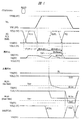
図1は、本発明の実施の形態1による半導体装置において、それに含まれる相変化メモリの読み出し動作の一例を示す波形図である。この読み出し動作の特徴は、読み出し動作初期に低電圧をビット線に印加し(プリチャージ)、読み出し動作(読み出し1)を行った後、センスアンプとチャージシェアすることによって、読み出しビット線に電荷を注入し、再度読み出し動作(読み出し2)を行うところにある。
(Embodiment 1)
FIG. 1 is a waveform diagram showing an example of a read operation of a phase change memory included in the semiconductor device according to the first embodiment of the present invention. The feature of this read operation is that a low voltage is applied to the bit line at the initial stage of the read operation (precharge), and after performing the read operation (read 1), the charge is shared with the sense amplifier, thereby charging the read bit line. The injection is performed and the read operation (read 2) is performed again.
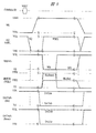
ここで、本動作の詳細を説明する前に、本読み出し動作を実現するための回路構成について説明する。図2は、本発明の実施の形態1による半導体装置において、それに含まれる相変化メモリの主要部の構成例を示すブロック図である。図2に示す構成例は、半導体基板上に形成され、その一部の回路として、メモリセルアレーMCAとセンスアンプブロックSABとロウデコーダRDECが含まれている。 Here, before describing the details of this operation, a circuit configuration for realizing this read operation will be described. FIG. 2 is a block diagram showing a configuration example of a main part of the phase change memory included in the semiconductor device according to the first embodiment of the present invention. The configuration example shown in FIG. 2 is formed on a semiconductor substrate, and includes a memory cell array MCA, a sense amplifier block SAB, and a row decoder RDEC as part of its circuit.
本構成例では、センスアンプブロックSABにおいて、4つのビット線BL0,BL1,BL2,BL3のうちビット線選択回路BLSELによって選ばれた1本が1つのセンスアンプ回路SAに接続される。ビット線選択回路BLSELは、本図には示していないが入力されたアドレスに対応して、4本のビット線のうち1本を選択し、そのビット線を、読み出し動作では読み出しビット線BLSAに接続し、書き込み動作では書き込みビット線WBLに接続する。 In this configuration example, one of the four bit lines BL0, BL1, BL2, and BL3 selected by the bit line selection circuit BLSEL is connected to one sense amplifier circuit SA in the sense amplifier block SAB. Although not shown in the figure, the bit line selection circuit BLSEL selects one of the four bit lines corresponding to the input address, and the bit line is selected as the read bit line BLSA in the read operation. In the write operation, the write bit line WBL is connected.
センスアンプ回路SAは、アレーのビット線に読み出された微小信号をリファレンスレベルVREFと比較することで、‘1’/‘0’の判定をし、アレー外部にセンスアンプ出力ノードSAO(図2では図示せず)を介してデータを出力する回路である。また、センスアンプ回路SAには、外部からのライトデータに従って書き込みビット線を利用してメモリセルにデータを書きこむための書き込み回路も配置される。各々の具体的な回路構成例については、後で述べる。 The sense amplifier circuit SA makes a determination of “1” / “0” by comparing the minute signal read out to the bit line of the array with the reference level VREF, and detects the sense amplifier output node SAO (see FIG. 2) outside the array. This is a circuit for outputting data via (not shown). The sense amplifier circuit SA is also provided with a write circuit for writing data into the memory cell using a write bit line in accordance with external write data. Each specific circuit configuration example will be described later.
図2に示した構成例は、例えば、図21に示すようなチップ内の主要部を示したものとなっている。図21は、図2の構成を含めた相変化メモリ全体の構成の一例を示すブロック図である。図21に示す相変化メモリは、そのチップ上に、例えば、メモリアレーMAと、それに隣接するロウデコーダRDECおよびカラムデコーダCDECと、電源回路VGと、外部からのコマンドおよびアドレスを受け入れる入力バッファ(INPUT Buffer)と,外部との間でデータの入出力を行う入出力バッファ(DQ Buffer)などが配置されている。電源回路VGは、内部電圧を外部電源VCCから生成する。ビット線のリファレンスレベルVREFもここで生成される。 The configuration example shown in FIG. 2 shows a main part in the chip as shown in FIG. 21, for example. FIG. 21 is a block diagram showing an example of the configuration of the entire phase change memory including the configuration of FIG. The phase change memory shown in FIG. 21 includes, for example, a memory array MA, a row decoder RDEC and a column decoder CDEC adjacent to the memory array MA, a power supply circuit VG, and an input buffer (INPUT that receives an external command and address). An input / output buffer (DQ Buffer) for inputting / outputting data between the buffer and the outside is arranged. The power supply circuit VG generates an internal voltage from the external power supply VCC. The bit line reference level VREF is also generated here.
メモリアレーMAは、複数のメモリセルアレーMCAに分割され、各メモリセルアレーMCAの間には、例えば、サブワードドライバSWDと、センスアンプブロックSABと、クロスエリアXAなどが含まれている。ここで、メモリアレーMAは多分割構成になっているが、分割しなくても良い。クロスエリアXAは、センスアンプブロックSABとサブワードドライバSWDの交差部分であり、主に、センスアンプブロック及び、サブワードドライバの制御信号を駆動する回路が配置される。 The memory array MA is divided into a plurality of memory cell arrays MCA. Between each memory cell array MCA, for example, a sub word driver SWD, a sense amplifier block SAB, a cross area XA, and the like are included. Here, the memory array MA has a multi-divided configuration, but it may not be divided. The cross area XA is an intersection of the sense amplifier block SAB and the sub word driver SWD, and mainly a circuit for driving the sense amplifier block and the control signal of the sub word driver is arranged.
図2に示した構成例は、このようなチップの中から、その1つのメモリセルアレーMCAの一部と、1つのセンスアンプブロックSABの一部と、ロウデコーダRDECの一部を示したものとなっている。 The configuration example shown in FIG. 2 shows a part of one memory cell array MCA, a part of one sense amplifier block SAB, and a part of the row decoder RDEC among such chips. It has become.
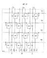
図3は、図2の構成例において、そのメモリセルアレーMCAの構成の一例を示す回路図である。図3に示すメモリセルアレーMCAは、ワード線WL0,WL1,WL2,WL3,・・・と、ビット線BL0,BL1,BL2,BL3と、これらのそれぞれ所望の交点にあるメモリセルMCからなる。また、ソース線SL01,SL23,・・・が設けられ、これらのソース線は、読み出し、書き込み、待機時で制御される制御線、もしくは、特定の電位(例えば、接地電位VSS)に接続される。ソース線SLは、共通のプレートとしてもよい。ここで、ビット線はデータ線とも呼ばれる。 FIG. 3 is a circuit diagram showing an example of the configuration of the memory cell array MCA in the configuration example of FIG. The memory cell array MCA shown in FIG. 3 includes word lines WL0, WL1, WL2, WL3,..., Bit lines BL0, BL1, BL2, BL3, and memory cells MC at respective desired intersections. Further, source lines SL01, SL23,... Are provided, and these source lines are connected to a control line that is controlled during reading, writing, and standby, or to a specific potential (for example, ground potential VSS). . The source line SL may be a common plate. Here, the bit line is also called a data line.
図4は、図3のメモリセルアレーにおいて、その各メモリセルの構成の一例を示す回路図であり、(a)、(b)には、それぞれ異なる構成例を示している。各メモリセルMCは、図4(a),(b)に示すように記憶素子PCRとメモリセルトランジスタMTにより構成される。図4(a)においては、記憶素子PCRの一端がビット線BLに接続され、他端がメモリセルトランジスタMTのソース・ドレインの一方に接続される。記憶素子PCRは、例えば、ゲルマニウム、アンチモン、テルルなどを含有したカルコゲナイド材料からなる。メモリセルトランジスタMTのソース・ドレインの他方は、ソース線SLに接続され、ゲートはワード線WLに接続される。 FIG. 4 is a circuit diagram showing an example of the configuration of each memory cell in the memory cell array of FIG. 3, and (a) and (b) show different configuration examples. Each memory cell MC includes a storage element PCR and a memory cell transistor MT as shown in FIGS. In FIG. 4A, one end of the storage element PCR is connected to the bit line BL, and the other end is connected to one of the source and drain of the memory cell transistor MT. The memory element PCR is made of a chalcogenide material containing, for example, germanium, antimony, tellurium and the like. The other of the source and drain of the memory cell transistor MT is connected to the source line SL, and the gate is connected to the word line WL.
また、メモリセル内の構成として、図4(b)のように図4(a)のメモリセルトランジスタMTと記憶素子PCRを入れ替えた構成でもかまわない。この構成では、ライト動作などでビット線BLを駆動しても、ワード線WLを非選択状態にしておくことでビット線BLから記憶素子PCRにAC的な電流が流れることを防止できる利点である。 Further, as a configuration in the memory cell, a configuration in which the memory cell transistor MT and the storage element PCR in FIG. 4A are interchanged as shown in FIG. 4B may be used. In this configuration, even when the bit line BL is driven by a write operation or the like, it is possible to prevent an AC current from flowing from the bit line BL to the storage element PCR by keeping the word line WL in a non-selected state. .
また、ここでは、メモリセルトランジスタMTとしてNMOSトランジスタを示しているが、PMOSトランジスタやバイポーラトランジスタの使用も可能である。ただし、高集積化と周辺回路とのプロセスコンパチビリティの観点からMOSトランジスタが望ましく、PMOSトランジスタに比べてオン状態でのチャネル抵抗の小さいNMOSトランジスタが好適である。以下では、メモリセルの構成として、図4(a)のような構成を前提とし、トランジスタにNMOSトランジスタを用いる場合の電圧関係で、動作などを説明する。 Here, an NMOS transistor is shown as the memory cell transistor MT, but a PMOS transistor or a bipolar transistor can also be used. However, a MOS transistor is desirable from the viewpoint of high integration and process compatibility with peripheral circuits, and an NMOS transistor having a smaller channel resistance in the on state than the PMOS transistor is preferable. In the following, the operation and the like will be described with respect to the voltage relationship when an NMOS transistor is used as the transistor on the premise of the configuration of the memory cell as shown in FIG.
図5は、図2の構成例において、そのセンスアンプブロック内のビット線選択回路の構成の一例を示す回路図である。ビット線選択回路BLSELには、読み出し動作において、入力されたアドレスに従ってメモリセルアレーMCA内のビット線BL0〜BL3のいずれかを選択する読み出しビット線選択信号RSEL0〜RSEL3と、読み出しビット線選択信号RSEL0〜RSEL3が入力され、ビット線BL0〜BL3のいずれかをセンスアンプ内の読み出しビット線BLSAに接続するスイッチと、読み出し動作と同様に、書き込み動作において、入力されたアドレスに従ってビット線BL0〜BL3のいずれかを選択する書き込みビット線選択信号WSEL0〜WSEL3と、書き込みビット線選択信号WSEL0〜WSEL3が入力され、ビット線BL0〜BL3のいずれかを書き込みビット線WBLに接続するスイッチが配置される。 FIG. 5 is a circuit diagram showing an example of the configuration of the bit line selection circuit in the sense amplifier block in the configuration example of FIG. In the read operation, the bit line selection circuit BLSEL has read bit line selection signals RSEL0 to RSEL3 for selecting any of the bit lines BL0 to BL3 in the memory cell array MCA according to the input address, and a read bit line selection signal RSEL0. To RSEL3, a switch for connecting any one of the bit lines BL0 to BL3 to the read bit line BLSA in the sense amplifier, and a read operation similar to the read operation, in the write operation, the bit lines BL0 to BL3 A write bit line selection signal WSEL0 to WSEL3 for selecting one of them and a write bit line selection signal WSEL0 to WSEL3 are inputted, and a switch for connecting any one of the bit lines BL0 to BL3 to the write bit line WBL is arranged.
また、これらに加えて、ビット線イコライズ信号EQ0〜EQ3で制御され、待機時の期間においてビット線BL0〜BL3を所定の電圧レベル、例えば、メモリセルMCのソース線電位VSに設定するスイッチと、ビット線プリチャージ信号PCA0〜PCA3で制御され、ビット線BL0〜BL3を読出し時の初期電圧レベル、例えばVRに設定するプリチャージスイッチと、センスアンププリチャージ信号PCSAで制御され、センスアンプ内の読み出しビット線BLSAを読み出し時の所定の電圧レベルVDLにプリチャージするスイッチが配置される。 In addition to these, a switch that is controlled by the bit line equalize signals EQ0 to EQ3 and sets the bit lines BL0 to BL3 to a predetermined voltage level, for example, the source line potential VS of the memory cell MC in the standby period; Controlled by bit line precharge signals PCA0 to PCA3, controlled by a precharge switch for setting bit lines BL0 to BL3 to an initial voltage level when reading, for example, VR, and a sense amplifier precharge signal PCSA, and reading in the sense amplifier A switch for precharging the bit line BLSA to a predetermined voltage level VDL at the time of reading is arranged.
ここで、ビット線プリチャージ信号PCA0〜3は、この4本全てが同一の制御信号(4本のビット線を1本のビット線プリチャージ信号で一斉に制御する方式)でもよいし、それぞれ、対応したアドレス信号によって制御される独立の信号でもかまわない。独立の信号とすることで、読み出し・書き込み非選択ビット線の無駄な充放電を防止できるため、消費電力を低減できる利点がある。一方、同一の信号とすることで、アドレスごとの制御が不要となるため、高速動作と制御信号の駆動回路が少なくなることによる小面積化を実現できる利点がある。また、ビット線イコライズ信号EQ0〜EQ3についても前述のプリチャージ信号と同様に、同一の制御信号でもよいし、それぞれアドレス信号に対応した独立な制御信号でもかまわない。そのときの利点は、前述のビット線プリチャージ信号の場合と同様である。 Here, all of the four bit line precharge signals PCA0 to PCA3 may be the same control signal (a method in which four bit lines are simultaneously controlled by one bit line precharge signal). An independent signal controlled by a corresponding address signal may be used. By using an independent signal, it is possible to prevent wasteful charging / discharging of the read / write non-selected bit lines, and there is an advantage that power consumption can be reduced. On the other hand, by using the same signal, control for each address becomes unnecessary, so that there is an advantage that a high-speed operation and a reduction in area can be realized by reducing the drive circuit for the control signal. Also, the bit line equalize signals EQ0 to EQ3 may be the same control signal as in the precharge signal described above, or may be independent control signals corresponding to the address signals. The advantages at that time are the same as those of the bit line precharge signal described above.
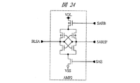
図6は、図2の構成例において、そのセンスアンプブロックに配置されるセンスアンプ回路の構成例である。センスアンプ回路SAは、メモリセルアレーMCAからセンスアンプ内の読み出しビット線BLSAに読み出された微小信号をセンスアンプ出力ノードSAOに出力するためのアンプ回路AMPと、外部からの書き込みデータを書き込みビット線WBLを介して、メモリセルMCの記憶素子PCRに書き込むためのライトドライバWDからなる。 FIG. 6 is a configuration example of a sense amplifier circuit arranged in the sense amplifier block in the configuration example of FIG. The sense amplifier circuit SA includes an amplifier circuit AMP for outputting a minute signal read from the memory cell array MCA to the read bit line BLSA in the sense amplifier to the sense amplifier output node SAO, and write data from the outside as a write bit. It comprises a write driver WD for writing to the storage element PCR of the memory cell MC via the line WBL.
図7は、図6のセンスアンプ回路において、そのアンプ回路の構成の一例を示す回路図である。図7に示すアンプ回路AMPは、電圧センス型のセンスアンプであり、対となるNMOSトランジスタNM1,NM2のそれぞれのゲートに、センスアンプ内の対となるビット線が接続されたゲート受けのアンプ回路である。対となるビット線の内の一方は、読み出しビット線BLSAであり、他方は、常にリファレンスレベルVREFが供給されるビット線である。それぞれのNMOSトランジスタNM1,NM2のドレインには、クロスカップル型のPMOSトランジスタが負荷として接続されている。NMOSトランジスタNM1,NM2のソースは、共通に接続され、アンプ回路駆動用のMOSトランジスタに接続されている。 FIG. 7 is a circuit diagram showing an example of the configuration of the amplifier circuit in the sense amplifier circuit of FIG. The amplifier circuit AMP shown in FIG. 7 is a voltage sense type sense amplifier, and is a gate receiving amplifier circuit in which a pair of bit lines in the sense amplifier is connected to each gate of the pair of NMOS transistors NM1 and NM2. It is. One of the paired bit lines is a read bit line BLSA, and the other is a bit line to which a reference level VREF is always supplied. A cross-coupled PMOS transistor is connected as a load to the drains of the NMOS transistors NM1 and NM2. The sources of the NMOS transistors NM1 and NM2 are connected in common and connected to the MOS transistor for driving the amplifier circuit.
アンプ回路AMPは、アンプ回路駆動用のMOSトランジスタのゲート信号であるセンスアンプ活性化信号SAEにより活性化される。本アンプ回路AMPでは、センスアンプ内の読み出しビット線BLSAがリファレンスレベルVREFよりも低い電位の場合には、センスアンプ出力ノードSAOに‘H’を出力し、読み出しビット線BLSAがリファレンスレベルVREFよりも高い電位の場合には、センスアンプ出力ノードSAOに‘L’を出力する。アンプ回路AMPの回路構成は、本回路構成に限定されるわけではなく、同様の機能があるものであればかまわない。 The amplifier circuit AMP is activated by a sense amplifier activation signal SAE which is a gate signal of a MOS transistor for driving the amplifier circuit. In the amplifier circuit AMP, when the read bit line BLSA in the sense amplifier has a potential lower than the reference level VREF, 'H' is output to the sense amplifier output node SAO, and the read bit line BLSA is lower than the reference level VREF. When the potential is high, 'L' is output to the sense amplifier output node SAO. The circuit configuration of the amplifier circuit AMP is not limited to this circuit configuration, and any circuit having the same function may be used.
図8は、図6のセンスアンプ回路において、そのライトドライバWDの構成の一例を示す回路図であり、(a)、(b)には、それぞれ異なる構成例を示している。図8(a)は、書き込み電圧を制御する方式となっている。すなわち、外部入力データ(データバス)DATAt/bに相補のデータが入力され、セットイネーブル信号WSとリセットイネーブル信号WRが高電位状態から低電位状態に遷移することで、活性化され、書き込みビット線WBLが高電位に駆動される。このとき、外部入力データDATAtが低電位状態、外部入力データDATAbが高電位状態の場合には、メモリセルMCをリセットする動作となり、書き込みビット線WBLには、リセット電圧VWRが印加される。 FIG. 8 is a circuit diagram showing an example of the configuration of the write driver WD in the sense amplifier circuit of FIG. 6, and (a) and (b) show different configuration examples. FIG. 8A shows a method for controlling the write voltage. That is, complementary data is input to the external input data (data bus) DATAt / b, and the set enable signal WS and the reset enable signal WR are activated by transition from the high potential state to the low potential state, and the write bit line WBL is driven to a high potential. At this time, when the external input data DATAt is in the low potential state and the external input data DATAb is in the high potential state, the memory cell MC is reset, and the reset voltage VWR is applied to the write bit line WBL.
リセット電圧VWRが書き込みビット線WBLに印加されると、ビット線選択回路BLSELを介してアレー内のビット線BL0,BL1,・・・のいずれかがリセット電圧VWRに駆動され、メモリセルMCの記憶素子PCRにリセット動作に必要な書き込み電流が供給される。このときの書き込みビット線WBLが駆動される期間は、リセットイネーブル信号WRが低電位に駆動されている期間で定義される。 When the reset voltage VWR is applied to the write bit line WBL, one of the bit lines BL0, BL1,... In the array is driven to the reset voltage VWR via the bit line selection circuit BLSEL, and the memory cell MC stores the data. A write current necessary for the reset operation is supplied to the element PCR. A period during which the write bit line WBL is driven at this time is defined as a period during which the reset enable signal WR is driven to a low potential.
逆に外部入力データDATAtが高電位状態、外部入力データDATAbが低電位状態の場合には、メモリセルMCをセットする動作となり、書き込みビット線WBLには、セット電圧VWSが印加される。セット電圧VWSが書き込みビット線WBLに印加されるとビット線選択回路BLSELを介してアレー内のビット線BL0,BL1,・・・のいずれかがセット電圧VWSに駆動され、メモリセルMCの記憶素子PCRにセット動作に必要な書き込み電流が流れる。このときの書き込みビット線WBLが駆動される期間は、セットイネーブル信号WSが低電位に駆動されている期間で定義され、セット動作の期間は、リセット動作の期間よりも長い。その後、いずれの動作においてもセット/リセットイネーブル信号WS/WRが高電位状態になることで、書き込みビット線WBLは、低電位(例えばソース線電位VS)に駆動され、ライト動作が終了する。 On the contrary, when the external input data DATAt is in the high potential state and the external input data DATAb is in the low potential state, the memory cell MC is set, and the set voltage VWS is applied to the write bit line WBL. When the set voltage VWS is applied to the write bit line WBL, one of the bit lines BL0, BL1,... In the array is driven to the set voltage VWS via the bit line selection circuit BLSEL, and the storage element of the memory cell MC A write current necessary for the set operation flows through the PCR. The period during which the write bit line WBL is driven is defined as the period during which the set enable signal WS is driven at a low potential, and the set operation period is longer than the reset operation period. Thereafter, in any operation, the set / reset enable signal WS / WR is brought into a high potential state, whereby the write bit line WBL is driven to a low potential (for example, the source line potential VS), and the write operation is completed.
図8(b)は、前述の図8(a)と異なり、書き込みデータに従って、書き込み電流をカレントミラー回路を用いて制御する方式となっている。ライトドライバWDには、書き込みリファレンス電流源WCGが配置され、ここでは、セット、リセット動作に必要な電流を生成するためのリファレンス電流Iwrefが生成される。本方式においては、トランジスタMPとの間でカレントミラー回路を構成するトランジスタMPRまたはトランジスタMPSのサイズ(ゲート長あるいはゲート幅)を変えて、カレントミラー回路のミラー比を設定することで、それぞれの書き込み動作時でリファレンス電流Iwrefの定数倍の電流が流れるようになっている。 FIG. 8B differs from the above-described FIG. 8A in that a write current is controlled using a current mirror circuit in accordance with write data. In the write driver WD, a write reference current source WCG is arranged, and here, a reference current Iwref for generating a current necessary for the set and reset operations is generated. In this method, each transistor MPR or transistor MPS constituting the current mirror circuit with the transistor MP is changed in size (gate length or gate width), and the mirror ratio of the current mirror circuit is set so that each writing is performed. During operation, a current that is a constant multiple of the reference current Iwref flows.
このとき、外部入力データDATAtが低電位状態、外部入力データDATAbが高電位状態の場合には、メモリセルMCをリセットする動作となり、書き込みビット線WBLには、リセット電流が流れる。リセット電流は、書き込みビット線WBLとビット線選択回路BLSELを介してアレー内のビット線BL0,BL1,・・・のいずれかに転送され、メモリセルMCの記憶素子PCRに流れる。このときの書き込みビット線WBLに書き込み電流が流れる期間は、リセットイネーブル信号WRが低電位に駆動されている期間で定義される。 At this time, when the external input data DATAt is in a low potential state and the external input data DATAb is in a high potential state, the memory cell MC is reset, and a reset current flows through the write bit line WBL. The reset current is transferred to one of the bit lines BL0, BL1,... In the array via the write bit line WBL and the bit line selection circuit BLSEL, and flows to the storage element PCR of the memory cell MC. A period during which a write current flows through the write bit line WBL at this time is defined as a period during which the reset enable signal WR is driven to a low potential.
逆に外部入力データDATAtが高電位状態、外部入力データDATAbが低電位状態の場合には、メモリセルMCをセットする動作となり、書き込みビット線WBLには、セット電流が流れる。セット電流は、書き込みビット線WBLとビット線選択回路BLSELを介してアレー内のビット線BL0,BL1,・・・のいずれかに転送され、メモリセルMCの記憶素子PCRに流れる。このときの書き込みビット線WBLに書き込み電流が流れる期間は、セットイネーブル信号WSが低電位に駆動されている期間で定義され、セット動作の期間は、リセット動作の期間よりも長い。その後、いずれの動作においてもセット/リセットイネーブル信号WS/WRが高電位状態になることで、書き込みビット線WBLは、低電位(例えばソース線電位VS)に駆動され、ライト動作が終了する。 Conversely, when the external input data DATAt is in a high potential state and the external input data DATAb is in a low potential state, the memory cell MC is set, and a set current flows through the write bit line WBL. The set current is transferred to one of the bit lines BL0, BL1,... In the array via the write bit line WBL and the bit line selection circuit BLSEL, and flows to the storage element PCR of the memory cell MC. A period during which a write current flows through the write bit line WBL at this time is defined as a period during which the set enable signal WS is driven to a low potential, and the set operation period is longer than the reset operation period. Thereafter, in any operation, the set / reset enable signal WS / WR is brought into a high potential state, whereby the write bit line WBL is driven to a low potential (for example, the source line potential VS), and the write operation is completed.
このような構成を備えた相変化メモリの読み出し動作について、前述した図1を用いて詳細に説明する。ここでは、メモリセルアレーMCA内のビット線BL0,BL1,BL2,BL3のうちビット線BL0を読み出す動作を例として説明する。 A read operation of the phase change memory having such a configuration will be described in detail with reference to FIG. Here, an operation of reading bit line BL0 out of bit lines BL0, BL1, BL2, and BL3 in memory cell array MCA will be described as an example.
外部より、読み出しコマンドREADが入力されると、同時に入力されるアドレスに対応したメモリセルアレーMCAにおいて、待機時にビット線BLをソース線SLと等電位に設定するためのビット線イコライズ信号EQ0が高電位状態から低電位状態に遷移することで非活性化され、アレー内のビット線BL0がフローティング状態となる。非選択ビット線BL1,BL2,BL3は、対応するビット線イコライズ信号EQ1,EQ2,EQ3を高電位に維持することでソース線SLの電位VSを維持し、メモリセルMC内の記憶素子PCRに対して、不要な電圧印加を防止して誤書換えを防止する。 When a read command READ is input from the outside, the bit line equalize signal EQ0 for setting the bit line BL to the same potential as the source line SL during standby is high in the memory cell array MCA corresponding to the simultaneously input address. The transition from the potential state to the low potential state deactivates the bit line BL0 in the array. The unselected bit lines BL1, BL2, BL3 maintain the potential VS of the source line SL by maintaining the corresponding bit line equalize signals EQ1, EQ2, EQ3 at a high potential, and with respect to the storage element PCR in the memory cell MC. Thus, unnecessary voltage application is prevented and erroneous rewriting is prevented.
続いて、ビット線プリチャージ信号PCA0が低電位状態から高電位状態に遷移することで活性化され、選択されたビット線BL0が読み出しビット線レベルVRに設定される。この読み出しビット線レベルVRは、記憶素子PCRに印加されても書換え動作にいたることのないような十分低い電圧である。このとき、非選択ビット線BL1,BL2,BL3は、待機時ビット線レベル(ソース線電位VS)を維持する。 Subsequently, the bit line precharge signal PCA0 is activated by transition from the low potential state to the high potential state, and the selected bit line BL0 is set to the read bit line level VR. The read bit line level VR is a sufficiently low voltage that does not cause a rewrite operation even when applied to the storage element PCR. At this time, the unselected bit lines BL1, BL2, and BL3 maintain the standby bit line level (source line potential VS).
ビット線BL0が読み出しビット線レベルVRに設定された後、ビット線プリチャージ信号PCA0は非活性化される。その後、読み出しコマンドREADと同時に入力されたアドレスに対応したワード線WLが低電位状態VWLから高電位状態VWHに遷移して活性化される。ワード線WLが活性化されると、メモリセルMCのメモリセルトランジスタMTが駆動され、記憶素子PCRに読み出しビット線レベルVRが印加される。 After the bit line BL0 is set to the read bit line level VR, the bit line precharge signal PCA0 is deactivated. Thereafter, the word line WL corresponding to the address input simultaneously with the read command READ is activated by transitioning from the low potential state VWL to the high potential state VWH. When the word line WL is activated, the memory cell transistor MT of the memory cell MC is driven, and the read bit line level VR is applied to the storage element PCR.
このとき、記憶素子PCRが高抵抗状態の場合、たとえば、相変化素子を用いた場合でアモルファス(非晶質)状態の時には、素子に流れる電流が小さいため、ビット線電位はプリチャージした読み出しビット線レベルVRからほとんど変化しない。図1では、プリチャージ〜読み出し1の期間におけるビット線BL0(Reset)のような波形になる。一方、記憶素子PCRが低抵抗状態の場合、たとえば、相変化素子を用いた場合で結晶状態の時には、素子に流れる電流が大きくなり、ビット線電位は、読み出しビット線レベルVRから、ソース線電位VSに遷移する。図1では、前述した期間におけるビット線BL0(Set)のような波形になる。 At this time, when the storage element PCR is in a high resistance state, for example, when a phase change element is used and in an amorphous state, the current flowing through the element is small, so that the bit line potential is the precharged read bit. Little change from line level VR. In FIG. 1, the waveform is similar to that of the bit line BL0 (Reset) in the period from precharge to readout 1. On the other hand, when the storage element PCR is in a low resistance state, for example, when a phase change element is used and in the crystalline state, the current flowing through the element increases, and the bit line potential changes from the read bit line level VR to the source line potential. Transition to VS. In FIG. 1, the waveform is like that of the bit line BL0 (Set) in the above-described period.
ワード線WLを活性化して一定期間経った後、アレーのビット線BL0とセンスアンプを接続するための読み出しビット線選択信号RSEL0が活性化される。これによって、図1における読み出し2の期間が開始される。このとき、センスアンプ内の読み出しビット線BLSAは、アレーのビット線BL0より高電位、例えばアレー電圧VDLにプリチャージされている。この状態で読み出しビット線選択信号RSEL0が活性化されると、センスアンプ内の読み出しビット線BLSAとアレー内のビット線BL0の間でチャージシェアが起こる。 After a certain period of time has passed since the word line WL is activated, the read bit line selection signal RSEL0 for connecting the array bit line BL0 and the sense amplifier is activated. As a result, the period of reading 2 in FIG. 1 is started. At this time, the read bit line BLSA in the sense amplifier is precharged to a higher potential than the array bit line BL0, for example, the array voltage VDL. When the read bit line selection signal RSEL0 is activated in this state, charge sharing occurs between the read bit line BLSA in the sense amplifier and the bit line BL0 in the array.
チャージシェア前のビット線レベルは、選択メモリセルの記憶素子PCRが低抵抗状態の場合、ソース線電位VSと等電位であり、高抵抗状態の場合、読み出しビット線レベルVRである。ここで、チャージシェアが起こると、それぞれ、低抵抗状態のときVDL×CSA/(CSA+CB)、高抵抗状態のときVR’=(VDL×CSA+VR×CB)/(CSA+CB)となる。ここで、CBはアレー内のビット線容量でCSAはセンスアンプ内の読み出しビット線BLSAの容量である。 The bit line level before charge sharing is equal to the source line potential VS when the storage element PCR of the selected memory cell is in the low resistance state, and is the read bit line level VR when the storage element PCR is in the high resistance state. Here, when charge sharing occurs, VDL × CSA / (CSA + CB) in the low resistance state and VR ′ = (VDL × CSA + VR × CB) / (CSA + CB) in the high resistance state, respectively. Here, CB is the bit line capacity in the array, and CSA is the capacity of the read bit line BLSA in the sense amplifier.
この間、ワード線WLは常に活性化状態のため、記憶素子PCRが低抵抗状態の場合には、引き続き、ビット線BL0の電荷は、ソース線SLに引き抜かれる。一方、高抵抗状態では、ビット線BL0のレベルは上昇するが、記憶素子PCRに流れる電流が小さいため、チャージシェア後のレベルがほとんど変化せず、維持される。この読み出し動作により、センスアンプ内の読み出しビット線BLSAは、リファレンスレベルVREFを適当に設定することで、高抵抗状態(Reset)では、リファレンスレベルより高電位側になり、低抵抗状態(Set)では、リファレンスレベルVREFよりも低電位側になる。 During this time, since the word line WL is always activated, when the storage element PCR is in the low resistance state, the charge of the bit line BL0 is continuously extracted to the source line SL. On the other hand, in the high resistance state, the level of the bit line BL0 rises, but since the current flowing through the storage element PCR is small, the level after charge sharing hardly changes and is maintained. By this read operation, the read bit line BLSA in the sense amplifier is appropriately set to the reference level VREF, so that it becomes higher than the reference level in the high resistance state (Reset), and in the low resistance state (Set). Therefore, the potential becomes lower than the reference level VREF.
その後、低抵抗状態の記憶素子PCRを読み出しているビット線がソース電位とほぼ等電位となる時間経過後、読み出しビット線選択信号RSEL0を非活性化状態にすることにより、アレー内のビット線BLとセンスアンプ内の読み出しビット線BLSAを分離する。それとほぼ同時に、アレー内のビット線BLを待機時電圧に設定するイコライズ信号EQが活性化状態になり、アレー内のビット線BLをソース線電位VSと等電位に設定する。そして、図1における読み出し2の期間が終了となる。このように、ビット線BLをソース線電位VSと等電位に設定することで、記憶素子PCRの両端に印加される電圧が0Vとなるため素子に電流が流れなくなり、発熱が防止でき、データ破壊が防止できる。 After that, after a lapse of time when the bit line reading the storage element PCR in the low resistance state becomes substantially equal to the source potential, the read bit line selection signal RSEL0 is deactivated to thereby inactivate the bit line BL in the array. And the read bit line BLSA in the sense amplifier are separated. At substantially the same time, the equalize signal EQ for setting the bit line BL in the array to the standby voltage is activated, and the bit line BL in the array is set to the same potential as the source line potential VS. Then, the period of reading 2 in FIG. 1 ends. In this manner, by setting the bit line BL to the same potential as the source line potential VS, the voltage applied to both ends of the storage element PCR becomes 0 V, so that no current flows through the element, heat generation can be prevented, and data destruction Can be prevented.
一方、センスアンプでは、センスアンプ活性化信号SAEによって活性化されることにより、センスアンプ内の読み出しビット線BLSAとリファレンスレベルVREFが比較され、センスアンプ出力ノードSAOに記憶内容に応じたデータが出力される。ここでは、低抵抗状態のときに高電位を出力し、高抵抗状態では、低電位を出力する。その後、ワード線WLを非活性化状態に遷移するとともに、センスアンプ内の読み出しビット線BLSAは、再びビット線選択回路BLSEL内のセンスアンププリチャージスイッチによって、アレー電圧VDLにプリチャージされる。 On the other hand, in the sense amplifier, when activated by the sense amplifier activation signal SAE, the read bit line BLSA in the sense amplifier is compared with the reference level VREF, and data corresponding to the stored contents is output to the sense amplifier output node SAO. Is done. Here, a high potential is output in the low resistance state, and a low potential is output in the high resistance state. Thereafter, the word line WL is changed to an inactivated state, and the read bit line BLSA in the sense amplifier is again precharged to the array voltage VDL by the sense amplifier precharge switch in the bit line selection circuit BLSEL.
以上のような読み出し方式を用いることで、ビット線に印加される読み出し電圧の低減またはビット線に高い読み出し電圧が印加される期間の短縮が可能となり、読み出し時の発熱を抑制して、誤書き込み等の読み出しデータ破壊を防止できる。また、読み出し電流に伴う熱ディスターブを防止できる。これによって、信頼性が高く安定した読み出し動作が可能となる。 By using the read method as described above, it is possible to reduce the read voltage applied to the bit line or shorten the period during which a high read voltage is applied to the bit line. It is possible to prevent read data destruction such as. In addition, it is possible to prevent thermal disturbance accompanying the read current. As a result, a reliable and stable read operation is possible.
すなわち、仮に本読み出し方式を用いない場合には、電圧VR’の振幅を備えた読み出し信号を得るために、例えば、図1において、ビット線に電圧VR’程度の電圧をその電圧が放電される期間印加することのみで読み出しを行う方式などが考えられる。これに比べて本方式を用いると、低抵抗状態(BL(set))の場合には、読み出しビット線レベルVR程度しか電圧が印加されず、高抵抗状態(BL(Reset))の場合でも、電圧VR’が印加される期間(読み出し2の期間)を短くすることが可能となる。例えば、図1の読み出し2の期間に示すように、低抵抗状態(BL(set))で放電される電圧が電圧VR’の半分程度になると、その分読み出し2の期間も半分程度となる。 That is, if this read method is not used, in order to obtain a read signal having the amplitude of the voltage VR ′, for example, in FIG. 1, the voltage is discharged to the bit line with a voltage of about VR ′. A method of performing reading only by applying a period can be considered. In contrast, when this method is used, in the low resistance state (BL (set)), only a voltage is applied to the read bit line level VR, and even in the high resistance state (BL (Reset)), It is possible to shorten the period during which the voltage VR ′ is applied (the period of reading 2). For example, as shown in the period of read 2 in FIG. 1, when the voltage discharged in the low resistance state (BL (set)) is about half of the voltage VR ′, the period of read 2 is also reduced to about half.
次に、書き込み動作について説明する。図9は、本発明の実施の形態1による半導体装置において、それに含まれる相変化メモリの書き込み動作の一例を示す波形図である。ここでは、ビット線BL1上のメモリセルMCに書き込む場合を想定して説明する。 Next, the write operation will be described. FIG. 9 is a waveform diagram showing an example of the write operation of the phase change memory included in the semiconductor device according to the first embodiment of the present invention. Here, description will be made assuming that data is written in the memory cell MC on the bit line BL1.
外部より、書き込みコマンドWRITが入力されると、コマンドと同時に入力されたアドレスに対応したビット線BL1のイコライズ信号EQ1が非活性化状態に遷移する。ここで、一旦読み出す場合には、前述の読み出し動作と同様の動作が行われる。その後、選択ビット線及び、非選択ビット線がソース線電位VSにプリチャージされた状態で、ワード線WLが活性化される。そして、外部から入力された書き込みデータがデータバスDATAt/bを使って転送されてくる。 When a write command WRIT is input from the outside, the equalize signal EQ1 of the bit line BL1 corresponding to the address input simultaneously with the command transitions to an inactive state. Here, when reading once, the same operation as the above-described reading operation is performed. Thereafter, the word line WL is activated in a state where the selected bit line and the unselected bit line are precharged to the source line potential VS. Then, write data input from the outside is transferred using the data bus DATAt / b.
センスアンプ回路SA中のライトドライバWDは、このデータバスDATAt/bの電位に従って、書き込みビット線WBLを駆動する。DATAtが高電位状態で、DATAbが低電位状態の場合には、セットイネーブル信号WSで決まるセット時間の間、ビット線BL1にセット書き込み電圧VWSが供給される。一方、データバスDATAtが低電位状態で、データバスDATAbが高電位状態の場合には、リセットイネーブル信号WRで決まるリセット時間の間、ビット線BL1にリセット書き込み電圧VWRが供給される。リセット時間は、通常セット時間に比べて短く、例えば10nsから100ns程度である。一方、セット時間は、通常、50nsから1us程度である。 The write driver WD in the sense amplifier circuit SA drives the write bit line WBL according to the potential of the data bus DATAt / b. When DATAt is in the high potential state and DATAb is in the low potential state, the set write voltage VWS is supplied to the bit line BL1 for the set time determined by the set enable signal WS. On the other hand, when the data bus DATAt is in the low potential state and the data bus DATAb is in the high potential state, the reset write voltage VWR is supplied to the bit line BL1 during the reset time determined by the reset enable signal WR. The reset time is shorter than the normal set time, and is, for example, about 10 ns to 100 ns. On the other hand, the set time is usually about 50 ns to 1 us.
その後、リセットイネーブル信号WR及びセットイネーブル信号WSが非活性化状態(ここでは、高電位状態)に遷移すると書き込み動作が終了する。その後、アレーのビット線BLは、ビット線イコライズ信号EQによって、再びソース線電位VSに固定される。連続した書き込み動作が行われない場合には、ここで、活性化していたワード線WLが非選択状態に遷移して、待機状態になる。この書き込み動作は、一旦読み出し動作を行った後、選択メモリセルだけ書き込む動作でも良いし、読み出し動作なしに選択メモリセルに書き込む動作でもよい。 Thereafter, when the reset enable signal WR and the set enable signal WS transition to an inactive state (here, a high potential state), the write operation is finished. Thereafter, the bit lines BL of the array are fixed to the source line potential VS again by the bit line equalize signal EQ. If the continuous write operation is not performed, the activated word line WL changes to the non-selected state and enters a standby state. This write operation may be an operation in which only the selected memory cell is written after the read operation is once performed, or an operation in which the selected memory cell is written without the read operation.
つぎに、これまでに説明した各回路ブロックの別の構成例について説明する。 Next, another configuration example of each circuit block described so far will be described.
図10は、図2の構成例において、図3とは異なるメモリセルアレーの構成例を示す回路図である。図3では、ワード線WLとビット線BLのすべての交点にメモリセルMCが配置されているのに対して、本構成例では、半分の交点に配置され、さらに、隣り合う2つの交点のうち1つだけにメモリセルMCが配置されている。すなわち、1本のビット線BL上では、交差するワード線1本おきにメモリセルMCが配置され、同様に、1本のワード線WL上では、交差するビット線1本おきにメモリセルMCが配置されているのが特徴となっている。本メモリセルアレーMCAにおけるメモリセルMCは、前述の図3の場合と同様に図4(a),(b)のいずれも適用可能である。このようなレイアウトでは、メモリセルトランジスタの面積を大きくすることができ、大きな電流駆動力を得られる利点がある。 FIG. 10 is a circuit diagram showing a configuration example of a memory cell array different from that in FIG. 3 in the configuration example of FIG. In FIG. 3, the memory cells MC are arranged at all the intersections of the word lines WL and the bit lines BL. In this configuration example, the memory cells MC are arranged at half the intersections, and further, of the two adjacent intersections. Only one memory cell MC is arranged. That is, on each bit line BL, memory cells MC are arranged every other word line intersecting. Similarly, on every other word line WL, memory cells MC are arranged every other bit line intersecting. It is characterized by being arranged. 4A and 4B can be applied to the memory cell MC in the memory cell array MCA as in the case of FIG. Such a layout has an advantage that the area of the memory cell transistor can be increased and a large current driving capability can be obtained.
図11は、図2の構成例において、図3とは更に異なるメモリセルアレーの構成例を示す回路図である。本構成例も、前述の図10と同様にワード線WLとビット線BLの交点のうち半分だけに、メモリセルMCが配置されている。本構成では、隣接する2つのメモリセルでビット線コンタクトを共有しており、1本のビット線上では、交差するワード線との交点のうち、メモリセルがある交点とない交点がそれぞれ2つずつ交互に配置される。一方、ワード線WL上では、交差するビット線BLとの交点のうち、ビット線1本おきにメモリセルMCが配置される。 FIG. 11 is a circuit diagram showing a configuration example of a memory cell array different from that in FIG. 3 in the configuration example of FIG. Also in this configuration example, the memory cells MC are arranged at only half of the intersections of the word lines WL and the bit lines BL as in FIG. In this configuration, two adjacent memory cells share a bit line contact, and on one bit line, there are two intersections with and without a memory cell at each intersection of intersecting word lines. Alternatingly arranged. On the other hand, on the word line WL, memory cells MC are arranged at every other bit line at the intersection with the intersecting bit line BL.
本メモリセルアレーMCAにおけるメモリセルMCは、前述の図3等と同様に図4(a),(b)のいずれも適用可能であるが、特に、トランジスタの拡散層を共有できる図4(b)のほうが好ましい。このようなレイアウトでは、図4(b)のメモリセルMCを用いることで、ビット線コンタクトを共通にすることができ、メモリセル面積を小さくすることが可能となり、高集積化を実現できる。 4A and 4B can be applied to the memory cell MC in the present memory cell array MCA as in the case of FIG. 3 and the like described above. In particular, FIG. ) Is preferred. In such a layout, by using the memory cell MC of FIG. 4B, the bit line contact can be made common, the area of the memory cell can be reduced, and high integration can be realized.
図12は、図2の構成例において、図3とは更に異なるメモリセルアレーの構成例を示す回路図である。本構成例は、前述の図10,図11と同様に、ワード線WLとビット線BLの交点のうち半分だけにメモリセルMCが配置されている。但し、本構成では、図11と異なり、ソース線コンタクトが隣接するメモリセルMC間で共有されている。1本のビット線上では、交差するワード線WLとの交点のうち、メモリセルMCがある交点とない交点が2つずつ交互に配置される。一方、ワード線WL上では、交差するビット線BLとの交点のうち、ビット線1本おきにメモリセルMCが配置される。 FIG. 12 is a circuit diagram showing a configuration example of a memory cell array different from FIG. 3 in the configuration example of FIG. In the present configuration example, the memory cells MC are arranged at only half of the intersections of the word lines WL and the bit lines BL, as in FIGS. 10 and 11 described above. However, in this configuration, unlike FIG. 11, the source line contact is shared between adjacent memory cells MC. On one bit line, of the intersections with the intersecting word lines WL, two intersections with and without the memory cells MC are alternately arranged. On the other hand, on the word line WL, memory cells MC are arranged at every other bit line at the intersection with the intersecting bit line BL.
本メモリセルアレーMCAにおけるメモリセルMCは、前述の図3等の場合と同様に図4(a),(b)のいずれも適用可能であるが、トランジスタの拡散層を共有できる図4(a)のほうが好ましい。このようなレイアウトでは、図4(a)のメモリセルを用いることで、ソース線コンタクト領域を共有することができ、メモリセル面積を小さくすることができ高集積化が可能となる。 4A and 4B can be applied to the memory cell MC in the memory cell array MCA as in the case of FIG. 3 and the like described above. However, the memory cell MC in FIG. ) Is preferred. In such a layout, by using the memory cell of FIG. 4A, the source line contact region can be shared, the memory cell area can be reduced, and high integration can be achieved.
図13は、本発明の実施の形態1による半導体装置において、図2とは異なる相変化メモリの主要部の構成例を示すブロック図である。図2では、センスアンプブロックSABの片側にメモリセルアレーMCAが配置されていたのに対して、図13では、センスアンプブロックSABの両側にメモリセルアレーMCAが配置されている。さらに、センスアンプブロックSABの左側に配置されたメモリセルアレーMCAのビット線BL0及びBL1と、センスアンプブロックSABの右側に配置されたメモリセルアレーMCAのビット線BL2及びBL3が共通のセンスアンプブロックSAB内のビット線選択回路BLSELに接続されている。また、ビット線選択回路BLSELは、センスアンプ回路SAに読み出しビット線BLSAと書き込みビット線WBLを介して接続されている。 FIG. 13 is a block diagram showing a configuration example of a main part of the phase change memory different from that in FIG. 2 in the semiconductor device according to the first embodiment of the present invention. In FIG. 2, the memory cell array MCA is arranged on one side of the sense amplifier block SAB, whereas in FIG. 13, the memory cell array MCA is arranged on both sides of the sense amplifier block SAB. Further, the sense amplifier block in which the bit lines BL0 and BL1 of the memory cell array MCA arranged on the left side of the sense amplifier block SAB and the bit lines BL2 and BL3 of the memory cell array MCA arranged on the right side of the sense amplifier block SAB are common. The bit line selection circuit BLSEL in the SAB is connected. The bit line selection circuit BLSEL is connected to the sense amplifier circuit SA via the read bit line BLSA and the write bit line WBL.
つまり、本構成例は、左右のメモリセルMCのいずれかが活性化されると、2つのメモリセルアレーMCAの間に配置されたセンスアンプブロックSABのセンスアンプ回路SAが活性化される共有センスアンプ構成となっている。このように、共通センスアンプ構成をとることにより、例えば図21に示すようなチップで、メモリアレーMAの部分を多分割アレーで構成することが容易となる。図21では、前述したように、1つのメモリアレーMAが、センスアンプブロックSABとサブワードドライバSWDによって多数のメモリセルアレーMCAに分割されている。ビット線選択回路BLSEL及びセンスアンプ回路SAは前述の構成と同様である。 That is, in the present configuration example, when any of the left and right memory cells MC is activated, the shared sense in which the sense amplifier circuit SA of the sense amplifier block SAB disposed between the two memory cell arrays MCA is activated. It has an amplifier configuration. In this way, by adopting the common sense amplifier configuration, it becomes easy to configure the memory array MA portion with a multi-division array, for example, with a chip as shown in FIG. In FIG. 21, as described above, one memory array MA is divided into a large number of memory cell arrays MCA by the sense amplifier block SAB and the sub word driver SWD. The bit line selection circuit BLSEL and the sense amplifier circuit SA are the same as those described above.
図14は、本発明の実施の形態1による半導体装置において、図2とは更に異なる相変化メモリの主要部の構成例を示すブロック図である。本構成例では、前述の図2と異なり、センスアンプブロックSABにおいて、2本のアレーのビット線が1つのビット線選択回路BLSELに接続され、そのうち1本がセンスアンプ回路SAに接続される。つまり、アレーのビット線2本に対してセンスアンプ回路SAを割り当てている。メモリセルアレーMCAの構成は、図3、及び図10〜図12のいずれも適用可能である。また、センスアンプ回路SAの構成は、前述した図7と同様である。 FIG. 14 is a block diagram showing a configuration example of the main part of the phase change memory different from FIG. 2 in the semiconductor device according to the first embodiment of the present invention. In this configuration example, unlike the above-described FIG. 2, in the sense amplifier block SAB, two array bit lines are connected to one bit line selection circuit BLSEL, and one of them is connected to the sense amplifier circuit SA. That is, the sense amplifier circuit SA is assigned to two bit lines of the array. As the configuration of the memory cell array MCA, any of FIG. 3 and FIGS. 10 to 12 can be applied. The configuration of the sense amplifier circuit SA is the same as that in FIG.
図15は、図14の構成例において、そのビット線選択回路の構成の一例を示す回路図である。図15のビット線選択回路BLSELには、前述の図5と同様に、入力されたアドレスに対応して、アレーの2本のビット線BLから読み出しビット線BLSAまたは書き込みビット線WBLに接続するビット線を選択するための、読み出しビット線選択信号RSEL0〜1および書き込みビット線選択信号WSEL0〜1と、読み出しビット線選択信号RSEL0〜1で制御され、アレー内のビット線BL0,BL1と読み出しビット線BLSAを接続するための読み出しビット線選択スイッチと、書き込みビット線選択信号WSEL0〜1で制御され、ビット線BL0,BL1と書き込みビット線WBLを接続するための書き込みビット線選択スイッチが配置される。 FIG. 15 is a circuit diagram showing an example of the configuration of the bit line selection circuit in the configuration example of FIG. In the bit line selection circuit BLSEL of FIG. 15, the bit connected to the read bit line BLSA or the write bit line WBL from the two bit lines BL of the array corresponding to the input address as in FIG. The bit lines BL0 and BL1 in the array and the read bit lines are controlled by the read bit line selection signals RSEL0 to 1 and the write bit line selection signals WSEL0 to 1 and the read bit line selection signals RSEL0 to 1 for selecting lines. A read bit line selection switch for connecting the BLSA and a write bit line selection switch for connecting the bit lines BL0 and BL1 and the write bit line WBL, which are controlled by the write bit line selection signals WSEL0 to WSEL1, are arranged.
さらに、待機時にビット線BL0,BL1をビット線待機時電圧、例えば、ソース線と同電位VSに設定するためのビット線イコライズ信号EQ0,1とこれらのイコライズ信号によって制御されるイコライズスイッチと、読み出し時にビット線BL0,BL1を所望のレベル、例えば、読み出しビット線レベルVRに設定するためのビット線プリチャージ信号PCA0,1およびプリチャージスイッチと、センスアンプ内の読み出しビット線BLSAを所望の読み出し電圧VDLに設定するためのセンスアンププリチャージ信号PCSAおよびセンスアンププリチャージスイッチも配置される。 Further, bit lines BL0 and BL1 are set to a bit line standby voltage, for example, the same potential VS as that of the source line, and equalize switches controlled by these equalize signals and read are set during standby. Sometimes the bit lines BL0 and BL1 are set to a desired level, for example, the bit line precharge signals PCA0 and PCA0 and precharge switches for setting the read bit line level VR, and the read bit line BLSA in the sense amplifier is set to a desired read voltage. A sense amplifier precharge signal PCSA and a sense amplifier precharge switch for setting to VDL are also arranged.
読み出しビット線レベルVRは、センスアンププリチャージ電圧VDLよりも低い。図14の構成例における読み出し動作は、前述した図1および図2ではメモリセルアレーMCAの4本のビット線のうち1本だけが読み出される動作なのに対して、ビット線2本に1本が読み出される動作となる。これ以外の動作は、図1の読み出し動作波形例で説明した動作と同様である。 The read bit line level VR is lower than the sense amplifier precharge voltage VDL. The read operation in the configuration example of FIG. 14 is an operation in which only one of the four bit lines of the memory cell array MCA is read in FIGS. 1 and 2 described above, whereas one read out is performed on two bit lines. Operation The other operations are the same as those described in the read operation waveform example of FIG.
本構成例は、前述の図2の構成例に比べて同時にセンスアンプに読み出すことの出来るビット数が多くなるため、大量のデータを読み出す動作に向いている。また、メモリセルアレーMCAを、前述したようなワード線とビット線の交点のうち半分にメモリセルが配置される構成とした場合、同時に読み出したメモリセルのデータをすべてセンスアンプに読み出すことが出来る利点がある。 This configuration example is suitable for an operation of reading a large amount of data because the number of bits that can be simultaneously read to the sense amplifier is larger than that of the configuration example of FIG. Further, when the memory cell array MCA is configured such that the memory cells are arranged at half of the intersections of the word lines and the bit lines as described above, all the data of the memory cells read at the same time can be read to the sense amplifier. There are advantages.
図16は、本発明の実施の形態1による半導体装置において、図2とは更に異なる相変化メモリの主要部の構成例を示すブロック図である。本構成例では、これまでに説明した構成例と異なり、センスアンプブロックSABにおいて、アレーのビット線1本に対して1つのセンスアンプ回路SAが接続される。それにより、1本のワード線WLを選択したときに多数のビットがセンスアンプに読み出すことが可能となり、一度に多数のデータを出力することが可能となる利点がある。本構成例に対応するメモリセルアレーMCAの構成は、図3、及び図10,11,12のいずれも適用可能であるが、すべてのビット線BLに対してセンスアンプ回路SAが接続されているため、1本のワード線WLを選択したときにすべてのビット線BLにメモリセルのデータが読み出される図3の構成が好適である。 FIG. 16 is a block diagram showing a configuration example of a main part of the phase change memory different from FIG. 2 in the semiconductor device according to the first embodiment of the present invention. In this configuration example, unlike the configuration examples described so far, one sense amplifier circuit SA is connected to one bit line of the array in the sense amplifier block SAB. Thereby, when one word line WL is selected, a large number of bits can be read to the sense amplifier, and there is an advantage that a large number of data can be output at a time. The configuration of the memory cell array MCA corresponding to this configuration example can be applied to either FIG. 3 or FIGS. 10, 11, and 12, but the sense amplifier circuit SA is connected to all the bit lines BL. Therefore, the configuration of FIG. 3 is preferred in which the memory cell data is read out to all the bit lines BL when one word line WL is selected.
図17は、図16の構成例において、そのビット線選択回路の構成の一例を示す回路図である。本構成例では、アレーのビット線BLに対してセンスアンプの読み出しビット線BLSAと書き込みビット線WBLがそれぞれ1対1で対応している。すなわち、本ビット線選択回路BLSELでは、読み出し動作と書き込み動作でアレーのビット線BLをセンスアンプの読み出しビット線BLSA、書き込みビット線WBLに接続するためのビット線選択信号RSEL,WSELおよびそのためのスイッチと、アレーのビット線BLを待機時の間、ソース線と等電位VSに設定するためのイコライズ信号EQおよびイコライズスイッチと、アレーのビット線BLを読み出しビット線レベルVRに設定するためのプリチャージ信号PCAおよびプリチャージスイッチと、読み出しビット線BLSAをアレー電圧VDLに設定するためのセンスアンププリチャージ信号PCSAおよびプリチャージスイッチが配置される。センスアンプ回路SAは前述の図6と同様の構成でかまわない。 FIG. 17 is a circuit diagram showing an example of the configuration of the bit line selection circuit in the configuration example of FIG. In this configuration example, the read bit line BLSA and the write bit line WBL of the sense amplifier correspond one-to-one with the bit line BL of the array. That is, in this bit line selection circuit BLSEL, bit line selection signals RSEL and WSEL for connecting the array bit line BL to the read bit line BLSA and the write bit line WBL of the sense amplifier in the read operation and the write operation, and switches for the same And the equalization signal EQ and equalization switch for setting the array bit line BL to the equipotential VS with the source line during standby, and the precharge signal PCA for setting the array bit line BL to the read bit line level VR. In addition, a precharge switch, a sense amplifier precharge signal PCSA and a precharge switch for setting read bit line BLSA to array voltage VDL are arranged. The sense amplifier circuit SA may have the same configuration as that shown in FIG.
図18は、図16の構成例において、その読み出し動作の一例を示す波形図である。図16の構成例では、すべての読み出しビット線にセンスアンプ回路SAが配置されているため、前述した図1の動作波形例と比べて非選択ビット線が無いのが特徴である。 FIG. 18 is a waveform diagram showing an example of the read operation in the configuration example of FIG. The configuration example of FIG. 16 is characterized in that there is no unselected bit line as compared with the operation waveform example of FIG. 1 described above because the sense amplifier circuits SA are arranged on all the read bit lines.
このように、図16の構成例を用いると、ビット線1本ごとにセンスアンプ回路を配置することにより、同時に読み出すことの出来るビット数が多くなるため、連続したデータ読み出し動作が高速に行える。さらに、DRAMのようなページ読み出し動作が容易に実現できる。 As described above, when the configuration example of FIG. 16 is used, by arranging the sense amplifier circuit for each bit line, the number of bits that can be read simultaneously increases, so that continuous data reading operation can be performed at high speed. Further, a page read operation like a DRAM can be easily realized.
(実施の形態2)
本実施の形態2では、これまでに説明したような構成および動作を用い、更に読み出し時のリファレンスレベルを生成する手法について述べる。本手法の特徴は、前述の読み出し動作と同様に、2段階で読み出すことにより、読み出し時に高電圧を印加する時間を短くしつつ読み出し信号量を大きくするとともに、更に、リファレンスレベルをチャージシェアで出力することにより、安定したリファレンスレベルを生成するところにある。まず、本読み出し動作を実現するための回路構成について説明する。
(Embodiment 2)
In the second embodiment, a method for generating a reference level at the time of reading using the configuration and operation as described above will be described. The feature of this method is that, in the same way as the above-mentioned read operation, the read signal amount is increased while shortening the time for applying the high voltage at the time of read, and the reference level is output with the charge share. By doing so, a stable reference level is generated. First, a circuit configuration for realizing this read operation will be described.
図19は、本発明の実施の形態2による半導体装置において、それに含まれる相変化メモリの主要部の構成例を示すブロック図である。図19では、メモリセルアレーMCAと、入力されたアドレスに対応したワード線WLを選択するためのロウデコーダRDECと、選択したメモリセルのデータをセンスし、外部に出力するためのセンスアンプブロックSABとが示されている。 FIG. 19 is a block diagram showing a configuration example of a main part of the phase change memory included in the semiconductor device according to the second embodiment of the present invention. In FIG. 19, a memory cell array MCA, a row decoder RDEC for selecting a word line WL corresponding to an input address, and a sense amplifier block SAB for sensing data of the selected memory cell and outputting the same to the outside Is shown.
センスアンプブロックSABには、ビット線選択回路BLSEL2とセンスアンプ回路SA2が配置される。ビット線選択回路BLSEL2は、入力されたアドレスに対応して、4本のビット線BL0〜3のうち1本を選択し、この選択したビット線を、読み出し動作時に読み出しビット線BLSAに接続し、書き込み動作時に書き込みビット線WBLに接続する。さらに、前述の図2等の場合と異なり、図19のビット線選択回路BLSEL2は、リファレンスレベルを出力するために、非選択のビット線をセンスアンプリファレンスビット線BLREFに接続する。 A bit line selection circuit BLSEL2 and a sense amplifier circuit SA2 are arranged in the sense amplifier block SAB. The bit line selection circuit BLSEL2 selects one of the four bit lines BL0-3 corresponding to the input address, and connects the selected bit line to the read bit line BLSA during the read operation. Connected to the write bit line WBL during a write operation. Further, unlike the case of FIG. 2 and the like described above, the bit line selection circuit BLSEL2 of FIG. 19 connects an unselected bit line to the sense amplifier reference bit line BLREF in order to output a reference level.
図20は、本発明の実施の形態2による半導体装置において、図19とは異なる相変化メモリの主要部の構成例を示すブロック図である。本構成例は、センスアンプブロックSABに対して、両側にメモリセルアレーMCAが配置され、1つのセンスアンプブロックSABを2つのメモリセルアレーMCAで共有する共有センスアンプ構成となっている。センスアンプブロックSABには、左右のアレーのいずれかのビット線をセンスアンプの読み出しビット線BLSAあるいは、書き込みビット線WBLに接続し、非選択のビット線をリファレンスビット線BLREFに接続するためのビット線選択回路BLSEL2と、読み出しビット線BLSAとリファレンスビット線BLREF間の信号電圧をもとに、メモリセルに記憶されたデータを外部に出力し、さらに、外部からのデータに従って、書き込みビット線WBLを駆動してメモリセルにデータ書き込むためのセンスアンプ回路SA2が配置されている。 20 is a block diagram showing a configuration example of a main part of a phase change memory different from that in FIG. 19 in the semiconductor device according to the second embodiment of the present invention. This configuration example has a shared sense amplifier configuration in which memory cell arrays MCA are arranged on both sides of the sense amplifier block SAB and one sense amplifier block SAB is shared by two memory cell arrays MCA. The sense amplifier block SAB includes a bit for connecting one of the left and right array bit lines to the read bit line BLSA or the write bit line WBL of the sense amplifier and connecting a non-selected bit line to the reference bit line BLREF. Based on the signal voltage between the line selection circuit BLSEL2 and the read bit line BLSA and the reference bit line BLREF, the data stored in the memory cell is output to the outside, and the write bit line WBL is set according to the external data. A sense amplifier circuit SA2 for driving and writing data in the memory cell is arranged.
このように、共通センスアンプ構成をとることにより、前述した図21に示すチップのように、メモリアレーMAの部分を多分割アレーで構成することが容易となる。また、このような構成により、ビット線1本当たりの容量が低減できるため、低消費電力化と高速動作が実現できる。 Thus, by adopting a common sense amplifier configuration, it becomes easy to configure the memory array MA portion as a multi-division array as in the chip shown in FIG. Further, with such a configuration, the capacity per bit line can be reduced, so that low power consumption and high speed operation can be realized.
次に、図19及び図20のメモリセルアレーMCAの構成について説明する。図19における好適なメモリセルアレーの構成は、前述の図10、図11、図12である。いずれもビット線とワード線の交点のうち半分にだけメモリセルが配置されている構成である。この構成を用いることにより、ワード線WLを選択したときに同一メモリセルアレーMCA内でメモリセルの接続されないビット線BLが存在するため、そのビット線BLをセンスアンプのリファレンスビット線BLREFに接続することが可能となる。 Next, the configuration of the memory cell array MCA shown in FIGS. 19 and 20 will be described. The preferred memory cell array configuration in FIG. 19 is the aforementioned FIG. 10, FIG. 11, and FIG. In either case, the memory cells are arranged at only half of the intersections between the bit lines and the word lines. By using this configuration, there is a bit line BL to which no memory cell is connected in the same memory cell array MCA when the word line WL is selected, so that the bit line BL is connected to the reference bit line BLREF of the sense amplifier. It becomes possible.
一方、図20のメモリセルアレーMCAの構成は、図3または、図10,11,12のいずれでもかまわない。リファレンスビット線BLREFに接続するビット線BLを、必ずしもワード線WLを活性化しているメモリセルアレーMCA内から選択する必要がなく、隣接するメモリセルアレーMCAのビット線BLを用いることも可能であるため、共有センスアンプ構成である図20では、すべての交点にメモリセルが配置される図3のようなメモリセルアレーの構成も適用可能である。 On the other hand, the configuration of the memory cell array MCA of FIG. 20 may be that of FIG. 3 or FIGS. It is not always necessary to select the bit line BL connected to the reference bit line BLREF from the memory cell array MCA in which the word line WL is activated, and it is also possible to use the bit line BL of the adjacent memory cell array MCA. Therefore, in FIG. 20, which is a shared sense amplifier configuration, the configuration of a memory cell array as shown in FIG. 3 in which memory cells are arranged at all intersections can also be applied.
図22は、図19及び図20の構成例において、そのビット線選択回路の構成の一例を示す回路図である。本構成例では、前述の図5と同様に、アレーのビット線BL0〜3から読み出しビット線BLSAに接続するための読み出しビット線選択信号RSEL0〜3およびそれによって制御される選択スイッチと、書き込みビット線選択信号WSEL0〜3およびそれによって制御される選択スイッチと、ビット線BL0〜3を待機時にソース線電位VSに設定するためのイコライズ信号EQ0〜3およびイコライズスイッチと、読出し時に選択したビット線を読み出しビット線レベルVRに設定するためのプリチャージ信号PCA0〜3およびプリチャージスイッチと、読み出しビット線BLSAを読出し時に所望のレベル(例えばVDL)に設定するセンスアンププリチャージ信号PCSAおよびセンスアンププリチャージスイッチが配置される。 FIG. 22 is a circuit diagram showing an example of the configuration of the bit line selection circuit in the configuration examples of FIGS. 19 and 20. In this configuration example, as in FIG. 5, the read bit line selection signals RSEL0 to RSEL3 for connecting the bit lines BL0 to BL3 of the array to the read bit line BLSA, the selection switches controlled thereby, and the write bit Line selection signals WSEL0 to 3 and selection switches controlled thereby, equalize signals EQ0 to EQ3 and equalization switches for setting bit lines BL0 to BL3 to source line potential VS during standby, and bit lines selected at the time of reading Precharge signals PCA0 to PCA3 and a precharge switch for setting to read bit line level VR, and sense amplifier precharge signal PCSA and sense amplifier precharge for setting read bit line BLSA to a desired level (for example, VDL) at the time of reading Switch is placed .
そして、本構成例では、更に、アレーのビット線BL0〜3を、読み出しビット線BLSAと対をなすリファレンスビット線BLREFに接続するためのリファレンス選択信号DSEL0〜3と、リファレンス選択信号で制御されるリファレンス選択スイッチと、前述した読み出しビット線BLSAと同様、読出し時にリファレンスビット線BLREFを所望のレベル(例えばVDL)に設定するセンスアンププリチャージ信号PCSAおよびセンスアンププリチャージスイッチが配置される。このリファレンス選択スイッチは、読み出し動作において、メモリセルが活性化されない非選択ビット線をセンスアンプ内のリファレンスビット線BLREFに接続する。これによって、読み出し動作によって、ビット線の容量とセンスアンプ内のリファレンスビット線BLREFの容量の間でのチャージシェアでリファレンスレベルを生成する。 In this configuration example, the array bit lines BL0 to BL3 are further controlled by reference selection signals DSEL0 to DSEL3 for connecting to the reference bit line BLREF paired with the read bit line BLSA and the reference selection signal. Like the read bit line BLSA described above, a reference selection switch, a sense amplifier precharge signal PCSA and a sense amplifier precharge switch that set the reference bit line BLREF to a desired level (for example, VDL) at the time of reading are arranged. This reference selection switch connects a non-selected bit line in which a memory cell is not activated to a reference bit line BLREF in the sense amplifier in a read operation. Thus, a reference level is generated by a charge share between the bit line capacitance and the reference bit line BLREF capacitance in the sense amplifier by a read operation.
図23は、図19及び図20の構成例において、そのセンスアンプ回路の構成の一例を示す回路図である。前述の図7のセンスアンプ回路SAでは、読み出しと書き込みデータバスを分離した構成であったが、図23のセンスアンプ回路SA2では、読み出しと書き込みデータバスを共通にしている。 FIG. 23 is a circuit diagram showing an example of the configuration of the sense amplifier circuit in the configuration examples of FIGS. 19 and 20. In the sense amplifier circuit SA of FIG. 7 described above, the read and write data buses are separated, but in the sense amplifier circuit SA2 of FIG. 23, the read and write data buses are shared.
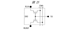
つまり、読み出し動作では、センスアンプ内の読み出しビット線BLSAとリファレンスビット線BLREFに相補の信号を読み出し、これらの信号をアンプ回路AMP2で増幅後、入出力ゲート部IOGを介して入出力線IOt/bに出力する。一方、書き込み動作では、外部から入力されたライトデータを、入出力線IOt/bおよび入出力ゲート部IOGを介して一旦読み出しビット線BLSAとリファレンスビット線BLREFに相補の信号として書き込む。そして、そのデータを用いて、ライトドライバWDが、書き込みビット線WBL、アレー内のビット線BLを介して、メモリセル内の記憶素子PCRにデータを書き込むことになる。 In other words, in the read operation, complementary signals are read to the read bit line BLSA and the reference bit line BLREF in the sense amplifier, these signals are amplified by the amplifier circuit AMP2, and then input / output line IOt / output to b. On the other hand, in the write operation, write data input from the outside is once written as complementary signals to the read bit line BLSA and the reference bit line BLREF via the input / output line IOt / b and the input / output gate unit IOG. Then, using the data, the write driver WD writes data to the storage element PCR in the memory cell via the write bit line WBL and the bit line BL in the array.
このように、本構成例では、一旦センスアンプ内の対となるビット線BLSA/BLREFにデータを書き込むことによって、入出力線IOt/bを占有している時間が短くできるため、入出力線IOt/bの動作サイクルを短くすることができる。ライトドライバWDの構成は、前述の図8(a),(b)に示されるいずれの構成に対し、データバスDATAt/DATAbの一方をリファレンスビット線BLREFに、他方を読み出しビット線BLSAに置き換えた構成でかまわない。 As described above, in this configuration example, the time for occupying the input / output line IOt / b can be shortened by writing data to the paired bit lines BLSA / BLREF in the sense amplifier. The operation cycle of / b can be shortened. The configuration of the write driver WD is such that one of the data buses DATAt / DATAb is replaced with a reference bit line BLREF and the other is replaced with a read bit line BLSA with respect to any of the configurations shown in FIGS. 8 (a) and 8 (b). Any configuration is acceptable.
図24は、図23のセンスアンプ回路において、そのアンプ回路の構成の一例を示す回路図である。本アンプ回路AMP2は、前述した書き込みデータを一旦保持する際にも利用可能なように、クロスカップル型のアンプを用いた構成となっている。 FIG. 24 is a circuit diagram showing an example of the configuration of the amplifier circuit in the sense amplifier circuit of FIG. The amplifier circuit AMP2 has a configuration using a cross-coupled amplifier so that the amplifier circuit AMP2 can be used to temporarily hold the write data.
図25は、図23のセンスアンプ回路において、その入出力ゲート部の構成の一例を示す回路図である。入出力ゲート部IOGでは、入力アドレスによって活性化されるカラム選択線YSによって、センスアンプ内の読み出しビット線BLSA、リファレンスビット線BLREFが入出力線IOt/bに接続され、データの授受を行う。なお、図24および図25で示した回路については、ここに示したものに限られるものでなく、同様の機能も有する回路構成であれば置き換えて利用することが可能である。 FIG. 25 is a circuit diagram showing an example of the configuration of the input / output gate section in the sense amplifier circuit of FIG. In the input / output gate section IOG, the column bit line YS activated by the input address connects the read bit line BLSA and the reference bit line BLREF in the sense amplifier to the input / output line IOt / b to exchange data. Note that the circuits shown in FIGS. 24 and 25 are not limited to those shown here, and any circuit configuration having a similar function can be used.
つぎに、前述したような構成を備えた相変化メモリの読み出し動作について説明する。図26は、本発明の実施の形態2による半導体装置において、それに含まれる相変化メモリの読み出し動作の一例を示す波形図である。本動作波形図では、ビット線BL0に接続されたメモリセルを、ビット線BL1をリファレンスとして読み出す動作を仮定している。また、メモリセルアレーMCAとしては、図11,12,13のようなワード線とビット線の交点のうち半分の交点にメモリセルMCが配置される構成を仮定している。 Next, a read operation of the phase change memory having the above-described configuration will be described. FIG. 26 is a waveform diagram showing an example of the read operation of the phase change memory included in the semiconductor device according to the second embodiment of the present invention. In this operation waveform diagram, it is assumed that the memory cell connected to the bit line BL0 is read using the bit line BL1 as a reference. The memory cell array MCA is assumed to have a configuration in which the memory cells MC are arranged at half of the intersections between the word lines and the bit lines as shown in FIGS.
図26において、外部より読み出しコマンドREADが入力されると、コマンドと同時に入力されたアドレスに従って、読み出し対象のメモリセルが接続されているビット線BL0とリファレンス用のビット線BL1のイコライズ信号EQ0,EQ1が非活性状態に遷移する。続いて、読み出し対象のメモリセルが接続されているビット線BL0のプリチャージ信号PCA0が活性化状態となり、ビット線BL0が読み出しビット線レベルVRにプリチャージされる。 In FIG. 26, when a read command READ is input from the outside, equalize signals EQ0 and EQ1 of the bit line BL0 to which the memory cell to be read is connected and the reference bit line BL1 are connected according to the address input simultaneously with the command. Transitions to the inactive state. Subsequently, the precharge signal PCA0 of the bit line BL0 to which the memory cell to be read is connected is activated, and the bit line BL0 is precharged to the read bit line level VR.
プリチャージされると、コマンドと同時に入力されたアドレスに対応したワード線WLが非選択状態から選択状態になる。これに従って、メモリセルの記憶素子PCRの抵抗状態によって、ビット線BL0の電位が変化する。ここで、メモリセルMCの記憶素子PCRが高抵抗状態の場合には、メモリセルMCを介して電流が流れないため、ビット線BL0の電位はほとんど変化せず、読み出しビット線レベルVRを保つ。一方、メモリセルMCの記憶素子PCRが低抵抗状態の場合には、メモリセルMCを介して電流が流れ、ビット線BL0の電位は、ソース線の電位VSに向かって遷移する。このとき、リファレンス用のビット線BL1は、ソース線電位VSを維持する。 When precharged, the word line WL corresponding to the address input simultaneously with the command is changed from the non-selected state to the selected state. Accordingly, the potential of the bit line BL0 changes depending on the resistance state of the storage element PCR of the memory cell. Here, when the storage element PCR of the memory cell MC is in a high resistance state, no current flows through the memory cell MC, so the potential of the bit line BL0 hardly changes and the read bit line level VR is maintained. On the other hand, when the storage element PCR of the memory cell MC is in a low resistance state, a current flows through the memory cell MC, and the potential of the bit line BL0 changes toward the potential VS of the source line. At this time, the reference bit line BL1 maintains the source line potential VS.
その後、ビット線BL0の読み出しビット線選択信号RSEL0とビット線BL1のリファレンスビット線選択信号DSEL1が活性化される。これにより、センスアンプ内の読み出しビット線BLSAとアレー内のビット線BL0の間でチャージシェアが起こり、ビット線BL0の電圧は、記憶素子PCRが低抵抗状態のときには、VDL×CSA/(CSA+CB)、高抵抗状態の時には、VR’=(VDL×CSA+VR×CB)/(CSA+CB)になる。ここで、CSAは、読み出しビット線BLSAの容量、CBは、アレー内のビット線BL0の容量を示す。一方、リファレンスビット線BL1は、センスアンプ内リファレンスビット線BLREFとの間でチャージシェアを行い、リファレンスビット線BLREFの容量と読み出しビット線BLSAの容量と同じとすると、VDL×CSA/(CSA+CB)に遷移する。 Thereafter, the read bit line selection signal RSEL0 for the bit line BL0 and the reference bit line selection signal DSEL1 for the bit line BL1 are activated. As a result, charge sharing occurs between the read bit line BLSA in the sense amplifier and the bit line BL0 in the array, and the voltage of the bit line BL0 is VDL × CSA / (CSA + CB) when the storage element PCR is in the low resistance state. In the high resistance state, VR ′ = (VDL × CSA + VR × CB) / (CSA + CB). Here, CSA represents the capacity of the read bit line BLSA, and CB represents the capacity of the bit line BL0 in the array. On the other hand, the reference bit line BL1 performs charge sharing with the reference bit line BLREF in the sense amplifier, and assuming that the capacity of the reference bit line BLREF and the capacity of the read bit line BLSA are the same, VDL × CSA / (CSA + CB). Transition.
その後、引き続きワード線は選択状態のままであるため、メモリセルが低抵抗状態のメモリセルには、読み出し電流が流れる。これにより、低抵抗状態の場合の読み出しビット線BL0の電位は、再びソース線電位VSに向かって遷移する。一方、メモリセルが高抵抗状態の場合には、チャージシェア後のビット線電位VR’を維持する。また、リファレンスとなるビット線BL1及びセンスアンプ内のリファレンスビット線BLREFは、チャージシェア後のレベル、VDL×CSA/(CSA+CB)を維持する。その結果、リファレンスビット線BLREFの電位、VDL×CSA/(CSA+CB)は、構造パラメータで決まるレベルであり、低抵抗状態のビット線電位VSと高抵抗状態のビット線電位VR’の間になり、センスアンプのリファレンス電位として用いることができる。 Thereafter, since the word line remains selected, a read current flows through the memory cell in which the memory cell is in the low resistance state. As a result, the potential of the read bit line BL0 in the low resistance state transitions again toward the source line potential VS. On the other hand, when the memory cell is in a high resistance state, the bit line potential VR 'after charge sharing is maintained. The reference bit line BL1 and the reference bit line BLREF in the sense amplifier maintain the level after charge sharing, VDL × CSA / (CSA + CB). As a result, the potential of the reference bit line BLREF, VDL × CSA / (CSA + CB), is at a level determined by the structural parameter, and is between the bit line potential VS in the low resistance state and the bit line potential VR ′ in the high resistance state, It can be used as a reference potential for the sense amplifier.
さらに、読出し時に低抵抗状態に印加される電圧が最大で読み出しビット線レベルVRなのに対して、読み出し信号量は、VR’=(VDL×CSA+VR×CB)/(CSA+CB)と大きくとることができ、読み出し動作での読み出し電流を小さくしつつ、読み出し信号量を大きく確保することができる。さらに、リファレンスレベルを非選択ビット線を用いて生成することにより、内部電圧変動の影響を受けにくく、安定した低電圧のリファレンスレベルを生成することができる利点がある。そして、これによって、信頼性が高い読み出し動作が可能となる。 Furthermore, while the maximum voltage applied to the low resistance state during reading is the read bit line level VR, the read signal amount can be as large as VR ′ = (VDL × CSA + VR × CB) / (CSA + CB), A large read signal amount can be ensured while reducing a read current in the read operation. Further, by generating the reference level using the non-selected bit line, there is an advantage that a stable low voltage reference level can be generated which is hardly affected by the internal voltage fluctuation. As a result, a highly reliable read operation is possible.
センスアンプ内のビット線対BLSA/BLREFに微小信号が読み出されたところで、読み出しビット線選択信号RSEL0とリファレンスビット線選択信号DSEL1が活性化状態から非選択状態に遷移する。これによって、読み出しビット線BLSA及びリファレンスビット線BLREFとアレー内のビット線BL0及びBL1が分離される。ビット線がそれぞれ分離されるとアレー内のビット線BL0,BL1は、イコライズ信号EQ0,EQ1が活性化されて、ビット線BL0,BL1をソース線レベルVSに設定する。これにより、記憶素子PCRに電圧が印加されなくなり、データ破壊を防止できる。 When a minute signal is read out to the bit line pair BLSA / BLREF in the sense amplifier, the read bit line selection signal RSEL0 and the reference bit line selection signal DSEL1 transition from the activated state to the non-selected state. As a result, the read bit line BLSA and the reference bit line BLREF are separated from the bit lines BL0 and BL1 in the array. When the bit lines are separated from each other, the equalize signals EQ0 and EQ1 are activated for the bit lines BL0 and BL1 in the array to set the bit lines BL0 and BL1 to the source line level VS. As a result, no voltage is applied to the storage element PCR, and data destruction can be prevented.
これとほぼ同時に、センスアンプ活性化信号SAEを活性化し、センスアンプ内のビット線対BLSA/BLREFの間の微小信号をセンスアンプ回路SA2のアンプ回路AMP2によって、ビット線振幅電圧VDLまで増幅する。その後、入力されたアドレスに対応したカラム選択信号YSが非選択レベルVSSから選択レベルVCLに活性化されることで、入出力ゲート部IOGが活性化され、入出力線IOt/bにメモリセルMCから読み出したデータが出力される。 At substantially the same time, the sense amplifier activation signal SAE is activated, and a minute signal between the bit line pair BLSA / BLREF in the sense amplifier is amplified to the bit line amplitude voltage VDL by the amplifier circuit AMP2 of the sense amplifier circuit SA2. Thereafter, the column selection signal YS corresponding to the input address is activated from the non-selection level VSS to the selection level VCL, whereby the input / output gate unit IOG is activated and the memory cell MC is connected to the input / output line IOt / b. The data read from is output.
データの出力が終了すると活性化していたワード線WLが選択状態の高電位状態VWHから非選択レベルVWLに遷移する。これとほぼ同時にセンスアンプ活性化信号SAEが非選択状態となるとともに、センスアンプ内のビット線対BLSA/BLREFは、センスアンププリチャージ信号PCSAが活性化されることでそれぞれアレー電圧VDLにプリチャージされ、待機状態となる。このとき、すべてのアレー内のビット線は、ソース線電位VSにプリチャージされ、記憶素子PCRとメモリセルトランジスタMTのソース・ドレイン間には、電圧が印加されず、ディスターブ電流が流れないためデータ破壊を防止できる。 When the data output ends, the activated word line WL transitions from the selected high potential state VWH to the unselected level VWL. At substantially the same time, the sense amplifier activation signal SAE is deselected, and the bit line pair BLSA / BLREF in the sense amplifier is precharged to the array voltage VDL by activating the sense amplifier precharge signal PCSA. And enters a standby state. At this time, the bit lines in all the arrays are precharged to the source line potential VS, and no voltage is applied between the storage element PCR and the source and drain of the memory cell transistor MT, and no disturb current flows, so that the data Destruction can be prevented.
図27は、本発明の実施の形態2による半導体装置において、図26とは異なる相変化メモリの読み出し動作の一例を示す波形図である。図27においては、前述したようなリファレンス電位をセンスアンプ領域で生成する方式において、センスアンプ回路SA2を前述した図6のセンスアンプ回路SAに置き換えた構成での動作波形を示している。前述の図26と比べて、ゲート受け型のアンプ回路AMPをもちいることにより、センスアンプ内のビット線対BLSA/BLREF(図6ではVREF)は読み出し動作における電圧レベルを維持し、アンプ回路AMPを活性化してもセンスアンプ出力ノードSAOが駆動されるだけで、センスアンプ内のビット線対BLSA/BLREFの電位は増幅されない。そのほかの動作は、前述の図26と同様である。 FIG. 27 is a waveform diagram showing an example of the read operation of the phase change memory different from that in FIG. 26 in the semiconductor device according to the second embodiment of the present invention. FIG. 27 shows an operation waveform in a configuration in which the sense amplifier circuit SA2 is replaced with the above-described sense amplifier circuit SA of FIG. 6 in the method of generating the reference potential as described above in the sense amplifier region. Compared with the above-described FIG. 26, by using the gate-receiving amplifier circuit AMP, the bit line pair BLSA / BLREF (VREF in FIG. 6) in the sense amplifier maintains the voltage level in the read operation, and the amplifier circuit AMP Even if activated, only the sense amplifier output node SAO is driven, and the potential of the bit line pair BLSA / BLREF in the sense amplifier is not amplified. Other operations are the same as those in FIG.
図28は、本発明の実施の形態2による半導体装置において、図19とは更に異なる相変化メモリの主要部の構成例を示すブロック図である。本構成では、センスアンプブロックSABにおいて、アレー内のビット線2本に対して1つのセンスアンプ回路SA2が配置される構成である。本構成におけるメモリセルアレーMCAの構成は、前述した図3、図10〜12のいずれでもかまわない。メモリアレーのビット線のうち、2本に1本のビット線がセンスアンプ回路SA2に接続され、外部に出力することができるため、大量のデータを出力、あるいは書き込む動作に向いている。 FIG. 28 is a block diagram showing a configuration example of a main part of a phase change memory different from FIG. 19 in the semiconductor device according to the second embodiment of the present invention. In this configuration, one sense amplifier circuit SA2 is arranged for two bit lines in the array in the sense amplifier block SAB. The configuration of the memory cell array MCA in this configuration may be any of the above-described FIG. 3 and FIGS. Of the bit lines of the memory array, one bit line is connected to the sense amplifier circuit SA2 and can be output to the outside, which is suitable for an operation of outputting or writing a large amount of data.
図29は、本発明の実施の形態2による半導体装置において、図19とは更に異なる相変化メモリの主要部の構成例を示すブロック図である。本構成では、センスアンプブロックSABにおいて、アレー内のビット線1本に対して1つのセンスアンプ回路SA2が配置される構成である。本構成におけるメモリセルアレーMCAの構成は、前述した図10、図11、図12も適用できるが、図3のようなビット線とワード線のすべての交点にメモリセルが配置される構成が好適である。すべてのビット線のデータをセンスアンプに読み出すことができるので、一度に大量のデータを読み書きする動作に向いている。 FIG. 29 is a block diagram showing a configuration example of a main part of a phase change memory different from FIG. 19 in the semiconductor device according to the second embodiment of the present invention. In this configuration, one sense amplifier circuit SA2 is arranged for one bit line in the array in the sense amplifier block SAB. The configuration of the memory cell array MCA in this configuration can also be applied to the above-described FIGS. 10, 11, and 12. However, a configuration in which memory cells are arranged at all intersections of bit lines and word lines as shown in FIG. 3 is preferable. It is. Since all the bit line data can be read out to the sense amplifier, it is suitable for reading and writing a large amount of data at a time.
図30は、図28及び図29の構成例において、そのビット線選択回路の構成の一例を示す回路図であり、(a)は、図28に対応した構成例、(b)は、図29に対応した構成例を示すものである。図30(a)に示すビット線選択回路BLSEL2は、前述した図15のビット線選択回路BLSELに対して、アレー内の2本のビット線BL0,BL1のいずれかをリファレンスビット線BLREFに接続するための信号およびスイッチ等が追加された構成となっている。図30(b)に示すビット線選択回路BLSEL2は、前述した図17のビット線選択回路BLSELに対して、アレー内の1本のビット線BL0をリファレンスビット線BLREFに接続するための信号およびスイッチ等が追加された構成となっている。これらリファレンスビット線BLREFに関連して追加する構成は、前述した図22の場合と同様であるため詳細な説明は省略する。 30 is a circuit diagram showing an example of the configuration of the bit line selection circuit in the configuration examples of FIGS. 28 and 29. FIG. 30A is a configuration example corresponding to FIG. 28, and FIG. The example of a structure corresponding to is shown. The bit line selection circuit BLSEL2 shown in FIG. 30A connects one of the two bit lines BL0 and BL1 in the array to the reference bit line BLREF in contrast to the bit line selection circuit BLSEL in FIG. For this purpose, a signal, a switch, and the like are added. The bit line selection circuit BLSEL2 shown in FIG. 30B is a signal and switch for connecting one bit line BL0 in the array to the reference bit line BLREF with respect to the bit line selection circuit BLSEL of FIG. Etc. are added. Since the configuration added in relation to the reference bit line BLREF is the same as that in the case of FIG. 22 described above, detailed description is omitted.
本実施の形態2の半導体装置の利点について述べる。本実施の形態では、前述の実施の形態1と同様に、読出し時に印加する電圧を低くすることにより、読み出し動作によるデータ破壊を防止しつつ、低電圧で2段階に分けて読み出すことにより読み出し印加電圧に比べて大きな読み出し信号を確保できる利点がある。さらに、本実施の形態では、低電圧のリファレンスレベルを読み出し非選択ビット線を利用して生成することにより、内部動作電圧変動を受けずに安定した低電圧のリファレンスレベルを生成することができる。 Advantages of the semiconductor device according to the second embodiment will be described. In the present embodiment, as in the first embodiment described above, the voltage applied at the time of reading is lowered to prevent data destruction due to the reading operation, and the read application is performed by reading in two steps at a low voltage. There is an advantage that a read signal larger than the voltage can be secured. Furthermore, in this embodiment, by generating a low voltage reference level by using a read non-selected bit line, it is possible to generate a stable low voltage reference level without being affected by internal operating voltage fluctuations.
以上、本発明者によってなされた発明を実施の形態に基づき具体的に説明したが、本発明は前記実施の形態に限定されるものではなく、その要旨を逸脱しない範囲で種々変更可能であることはいうまでもない。 As mentioned above, the invention made by the present inventor has been specifically described based on the embodiment. However, the present invention is not limited to the embodiment, and various modifications can be made without departing from the scope of the invention. Needless to say.
本発明は、相変化素子の書換え電流が低減できる180nm以下の加工技術を用いた半導体装置に適用するのが望ましい。また、より大きなプロセス世代においても、相変化素子へのコンタクト面積を低減することで、同様の効果が得られる。また、より微細化の進んだ世代に適用できることは言うまでもない。さらに、動作電圧として、外部電源電圧VCCは、2.5V,1.8V、1.5Vあるいはそれ以下が望ましい。低電圧化すると消費電力が抑えられ、また、デバイスに印加される電圧が低下するので信頼性が向上する。 The present invention is preferably applied to a semiconductor device using a processing technique of 180 nm or less that can reduce the rewrite current of the phase change element. Further, even in a larger process generation, the same effect can be obtained by reducing the contact area to the phase change element. Needless to say, the present invention can be applied to generations with further miniaturization. Further, as the operating voltage, the external power supply voltage VCC is preferably 2.5V, 1.8V, 1.5V or less. When the voltage is lowered, power consumption is suppressed, and the voltage applied to the device is reduced, so that reliability is improved.
ワード線の非選択レベルVWLは、0V以下の電源とするとよい。0Vにすると特別な電源回路が不要であり、チップ面積を低減できる。また、負電源とすることで、電流駆動力を向上させるためにメモリセルトランジスタを低しきい値としたときでも待機時のサブスレッショルド電流を低減でき、低消費電力になるだけでなく、非選択時の相変化素子に流れる電流を低減でき、リード・ライト非選択メモリセルのディスターブを抑制でき、データ信頼性、膜信頼性を向上できる。 The non-selection level VWL of the word line is preferably a power supply of 0V or less. When the voltage is set to 0 V, a special power supply circuit is unnecessary and the chip area can be reduced. In addition, by using a negative power supply, the subthreshold current during standby can be reduced even when the memory cell transistor is set to a low threshold in order to improve current driving capability. Current flowing through the phase change element can be reduced, disturbance of read / write non-selected memory cells can be suppressed, and data reliability and film reliability can be improved.
ワード線選択レベルVWHは、2.5V、1.8V、1.5Vなど外部電源電圧と等しくすることが望ましい。また、周辺回路電源と同じ電圧を用いても良い。さらに、メモリセルトランジスタの電流駆動力を確保するために、内部昇圧電源を用いて2.0Vもしくは、2.5Vなどの高電圧を用いてもよい。ソース線レベルVSはグランドレベルVSSと等しくすることにより、別途電源回路が不要となり、面積を低減できる。グランドレベルVSSは0Vである。周辺回路電圧VCL及びアレー電圧VDLは、1.0Vから1.8V程度が望ましい。また、アレー電圧は、周辺回路電圧よりも低電圧とすると低消費電力化できる利点がある。この範囲であると、通常のCMOSプロセスによる周辺トランジスタが流用でき、メモリセル特有のプロセスが不要となり、プロセス簡易化ができる。 The word line selection level VWH is preferably equal to an external power supply voltage such as 2.5V, 1.8V, 1.5V. Further, the same voltage as the peripheral circuit power supply may be used. Furthermore, in order to ensure the current driving capability of the memory cell transistor, a high voltage such as 2.0 V or 2.5 V may be used using an internal boost power supply. By making the source line level VS equal to the ground level VSS, a separate power supply circuit becomes unnecessary and the area can be reduced. The ground level VSS is 0V. The peripheral circuit voltage VCL and the array voltage VDL are preferably about 1.0V to 1.8V. Further, if the array voltage is lower than the peripheral circuit voltage, there is an advantage that the power consumption can be reduced. Within this range, peripheral transistors by a normal CMOS process can be diverted, a process peculiar to a memory cell becomes unnecessary, and the process can be simplified.
書き込み電圧のうちリセット書き込み電圧VWRは、周辺回路電圧と等しいかあるいは、ワード線選択レベルVWHと等しくすることが望ましい。高電圧を用いることで、小さいメモリセルトランジスタでも大きな電流を確保でき、小面積化を実現できる。セット書き込み電圧は、周辺回路電圧VCLと等しいかあるいは、それ以下にすることが望ましい。低電圧とすることで、書き込み時の電流がリセット動作に比べて小さくすることができ、誤ったリセット動作を防止できる。 Of the write voltages, the reset write voltage VWR is preferably equal to the peripheral circuit voltage or equal to the word line selection level VWH. By using a high voltage, a large current can be secured even with a small memory cell transistor, and a small area can be realized. The set write voltage is preferably equal to or lower than the peripheral circuit voltage VCL. By using a low voltage, the current at the time of writing can be reduced compared to the reset operation, and an erroneous reset operation can be prevented.
また、読み出しビット線レベルVRは、素子読み出し時にディスターブにならない電圧、例えば、0.2V〜0.4V程度が望ましい。本発明でのリファレンスレベルVREFは、読み出しビット線レベルVRと等しくすることにより、電源回路を共有化できるとともに、読出し時の電源ノイズを同相ノイズとしてキャンセルすることができる。さらに、本発明は、単品のメモリチップに適用しても良いし、さらには、論理混載メモリに適用しても良い。 The read bit line level VR is preferably a voltage that does not disturb when reading the element, for example, about 0.2V to 0.4V. By making the reference level VREF in the present invention equal to the read bit line level VR, the power supply circuit can be shared and the power supply noise at the time of reading can be canceled as in-phase noise. Furthermore, the present invention may be applied to a single memory chip, or may be applied to a logic mixed memory.
本発明の半導体装置は、特に相変化材料を用いた例えば、高密度集積メモリ回路、およびメモリ回路と論理回路が同一半導体基板に設けられたロジック混載型メモリ、およびアナログ回路を有する半導体装置に適用して有益な技術である。 The semiconductor device of the present invention is applied to, for example, a high-density integrated memory circuit using a phase change material, a logic embedded memory in which a memory circuit and a logic circuit are provided on the same semiconductor substrate, and a semiconductor device having an analog circuit. It is a useful technique.
WL,WL0,WL1,WL2,WL3 ワード線
VWH ワード線選択レベル
VWL ワード線非選択レベル
EQ,EQ0,EQ1,EQ2,EQ3 ビット線イコライズ信号
PCA,PCA0,PCA1,PCA2,PCA3 ビット線プリチャージ信号
BL,BL0,BL1,BL2,BL3 ビット線
BLREF リファレンスビット線
BLSA 読み出しビット線
BLSEL,BLSEL2 ビット線選択回路
VDL アレー電圧
VSS グラウンド電位
VS ソース線電位
SAE センスアンプ活性化信号
PCSA センスアンププリチャージ信号
VCL 周辺回路電源電圧
SAO センスアンプ出力ノード
VREF リファレンスレベル
RDEC ロウデコーダ
MCA メモリセルアレー
WBL 書き込みビット線
SAB センスアンプブロック
SA,SA2 センスアンプ回路
AMP,AMP2 アンプ回路
MC メモリセル
SL,SL01,SL23 ソース線
MT メモリセルトランジスタ
PCR 記憶素子
VR 読み出しビット線レベル
WSEL0,WSEL1,WSEL2,WSEL3 書き込みビット線選択信号
RSEL0,RSEL1,RSEL2,RSEL3 読み出しビット線選択信号
WD ライトドライバ
DATAt/b 書き込みデータバス
WR リセットイネーブル信号
WS セットイネーブル信号
MPR リセット電流供給トランジスタ
MPS セット電流供給トランジスタ
MP 書き込み電流リファレンストランジスタ
WCG 書き込みリファレンス電流生成回路
XA クロスエリア
CDEC カラムデコーダ
YS カラム選択信号
IOG 入出力ゲート部
IOt/b 入出力線
VG 電源回路
WL, WL0, WL1, WL2, WL3 Word line VWH Word line selection level VWL Word line non-selection level EQ, EQ0, EQ1, EQ2, EQ3 Bit line equalization signal PCA, PCA0, PCA1, PCA2, PCA3 Bit line precharge signal BL , BL0, BL1, BL2, BL3 bit line BLREF reference bit line BLSA read bit line BLSEL, BLSEL2 bit line selection circuit VDL array voltage VSS ground potential VS source line potential SAE sense amplifier activation signal PCSA sense amplifier precharge signal VCL peripheral circuit Power supply voltage SAO Sense amplifier output node VREF Reference level RDEC Row decoder MCA Memory cell array WBL Write bit line SAB Sense amplifier block SA, SA2 Sense amplifier circuit AMP, AMP2 Amplifier circuit MC Memory cell SL, SL01, SL23 Source line MT Memory cell transistor PCR Storage element VR Read bit line level WSEL0, WSEL1, WSEL2, WSEL3 Write bit line selection signal RSEL0, RSEL1, RSEL2, RSEL3 Read bit line selection signal WD Write driver DATAt / b Write data bus WR Reset enable signal WS Set enable signal MPR Reset current supply transistor MPS Set current supply transistor MP Write current reference transistor WCG Write reference current generation circuit XA Cross area CDEC Column decoder YS Column selection signal IOG I / O gate unit IOt / Input and output line VG power supply circuit
Claims (11)
前記複数のワード線と交差する第1及び第2ビット線と、
前記複数のワード線と前記第1及び第2ビット線の任意の交点に配置される複数の第1メモリセルと、
前記複数の第1メモリセルからの情報を増幅するセンスアンプと、
前記センスアンプに接続される第3ビット線及び第4ビット線と、
前記第1ビット線に第1電位を与える第1スイッチと、
前記第2ビット線に第2電位を与える第2スイッチと、
前記第3ビット線に第3電位を与える第3スイッチと、
前記第4ビット線に前記第3電位を与える第4スイッチと、
前記第1ビット線と前記第3ビット線を接続するための第5スイッチと、
前記第2ビット線と前記第4ビット線を接続するための第6スイッチとを有し、
前記第2スイッチにより前記第2ビット線に前記第2電位が、前記第3スイッチにより前記第3ビット線に前記第3電位が、前記第4スイッチにより前記第4ビット線に前記第3電位が与えられた状態で、前記第1スイッチが活性化され、第1の期間を経過した後、前記第1スイッチの非活性化及び前記複数のワード線のいずれか一つの活性化が行われ、第2の期間を経過した後、前記第5及び第6スイッチが第3の期間活性化され、
前記第1電位は、前記第2電位よりも高く、
前記第3電位は、前記第1電位よりも高いことを特徴とする半導体装置。 Multiple word lines,
First and second bit lines intersecting the plurality of word lines;
A plurality of first memory cells disposed at any intersection of the plurality of word lines and the first and second bit lines;
A sense amplifier for amplifying information from the plurality of first memory cells;
A third bit line and a fourth bit line connected to the sense amplifier;
A first switch for applying a first potential to the first bit line;
A second switch for applying a second potential to the second bit line;
A third switch for applying a third potential to the third bit line;
A fourth switch for applying the third potential to the fourth bit line;
A fifth switch for connecting the first bit line and the third bit line;
A sixth switch for connecting the second bit line and the fourth bit line;
The second switch applies the second potential to the second bit line, the third switch applies the third potential to the third bit line, and the fourth switch applies the third potential to the fourth bit line. In a given state, the first switch is activated, and after the first period has elapsed, the first switch is deactivated and one of the plurality of word lines is activated. After a period of 2 has elapsed, the fifth and sixth switches are activated for a third period ,
The first potential is higher than the second potential;
The semiconductor device , wherein the third potential is higher than the first potential .
前記第1ビット線には、前記第2電位を与える第7スイッチが接続され、
前記第3の期間を経過後、前記第5及び第6スイッチが非活性化され、前記センスアンプが活性化され、前記第2及び第7スイッチが活性化されることを特徴とする半導体装置。 The semiconductor device according to claim 1 ,
A seventh switch for applying the second potential is connected to the first bit line.
The semiconductor device, wherein after the third period has elapsed, the fifth and sixth switches are deactivated, the sense amplifier is activated, and the second and seventh switches are activated.
前記半導体装置は、更に、前記第1ビット線に第13スイッチを介して接続される第6ビット線を有し、
前記センスアンプは、読み出し時に信号を増幅して出力するアンプ回路と書き込み時に書き込み対象となる前記第1メモリセルに必要な電流を供給するライトドライバとを有し、
前記アンプ回路は、前記第3及び第4ビット線に接続され、
前記ライトドライバは、前記第6ビット線に接続されることを特徴とする半導体装置。 The semiconductor device according to claim 1 ,
The semiconductor device further includes a sixth bit line connected to the first bit line via a thirteenth switch,
The sense amplifier has an amplifier circuit that amplifies and outputs a signal at the time of reading, and a write driver that supplies a current necessary for the first memory cell to be written at the time of writing,
The amplifier circuit is connected to the third and fourth bit lines;
The semiconductor device, wherein the write driver is connected to the sixth bit line.
前記半導体装置は、共通ソース線を更に有し、
前記複数の第1メモリセルのそれぞれは、可変抵抗素子と、第1MISFETとを有し、
前記可変抵抗素子の一端は、前記第1ビット線に接続され、
前記可変抵抗素子の他端は、前記第1MISFETのソース又はドレインの一方に接続され、
前記第1MISFETのゲートは、前記複数のワード線のいずれか一つに接続され、
前記第1MISFETのソース又はドレインの他方は、前記共通ソース線に接続されていることを特徴とする半導体装置。 The semiconductor device according to claim 1 ,
The semiconductor device further includes a common source line,
Each of the plurality of first memory cells includes a variable resistance element and a first MISFET.
One end of the variable resistance element is connected to the first bit line,
The other end of the variable resistance element is connected to one of the source and drain of the first MISFET,
A gate of the first MISFET is connected to any one of the plurality of word lines;
The other of the source and the drain of the first MISFET is connected to the common source line.
前記半導体装置は、共通ソース線を更に有し、
前記複数の第1メモリセルのそれぞれは、可変抵抗素子と、第1MISFETとを有し、
前記可変抵抗素子の一端は、前記共通ソース線に接続され、
前記可変抵抗素子の他端は、前記第1MISFETのソース又はドレインの一方に接続され、
前記第1MISFETのゲートは、前記複数のワード線のいずれか一つに接続され、
前記第1MISFETのソース又はドレインの他方は、前記第1ビット線に接続されていることを特徴とする半導体装置。 The semiconductor device according to claim 1 ,
The semiconductor device further includes a common source line,
Each of the plurality of first memory cells includes a variable resistance element and a first MISFET.
One end of the variable resistance element is connected to the common source line,
The other end of the variable resistance element is connected to one of the source and drain of the first MISFET,
A gate of the first MISFET is connected to any one of the plurality of word lines;
The other of the source and the drain of the first MISFET is connected to the first bit line.
前記共通ソース線には、前記第2電位が与えられることを特徴とする半導体装置。 The semiconductor device according to claim 4 or 5 ,
2. The semiconductor device according to claim 1, wherein the second potential is applied to the common source line.
前記半導体装置は、更に、
前記第1ビット線に前記第2電位を与える第7スイッチと、
前記第2ビット線に前記第1電位を与える第8スイッチと、
前記第2ビット線と前記第3ビット線を接続する第9スイッチと、
前記第1ビット線と前記第4ビット線を接続する第10スイッチとを有することを特徴とする半導体装置。 The semiconductor device according to claim 1 ,
The semiconductor device further includes:
A seventh switch for applying the second potential to the first bit line;
An eighth switch for applying the first potential to the second bit line;
A ninth switch connecting the second bit line and the third bit line;
A semiconductor device comprising: a tenth switch connecting the first bit line and the fourth bit line.
前記半導体装置は、更に、
前記複数のワード線と交差する第5ビット線と、
前記第5ビット線と前記第3ビット線を接続する第11スイッチとを有することを特徴とする半導体装置。 The semiconductor device according to claim 7 .
The semiconductor device further includes:
A fifth bit line intersecting the plurality of word lines;
A semiconductor device comprising: the fifth bit line and an eleventh switch for connecting the third bit line.
前記半導体装置は、更に、前記第5ビット線に前記第1電位を与える第12スイッチを有することを特徴とする半導体装置。 The semiconductor device according to claim 8 .
The semiconductor device further includes a twelfth switch for applying the first potential to the fifth bit line.
前記半導体装置は、待機時に、前記第2及び第7スイッチが活性化されることを特徴とする半導体装置。 The semiconductor device according to claim 2 ,
In the semiconductor device, the second and seventh switches are activated during standby.
前記可変抵抗素子は、カルコゲナイド材料を含むことを特徴とする半導体装置。 The semiconductor device according to claim 4 or 5 ,
The variable resistance element includes a chalcogenide material.
Priority Applications (3)
| Application Number | Priority Date | Filing Date | Title |
|---|---|---|---|
| JP2004374314A JP4606869B2 (en) | 2004-12-24 | 2004-12-24 | Semiconductor device |
| US11/313,833 US7239562B2 (en) | 2004-12-24 | 2005-12-22 | Semiconductor device |
| US11/797,843 US7336544B2 (en) | 2004-12-24 | 2007-05-08 | Semiconductor device |
Applications Claiming Priority (1)
| Application Number | Priority Date | Filing Date | Title |
|---|---|---|---|
| JP2004374314A JP4606869B2 (en) | 2004-12-24 | 2004-12-24 | Semiconductor device |
Publications (3)
| Publication Number | Publication Date |
|---|---|
| JP2006179158A JP2006179158A (en) | 2006-07-06 |
| JP2006179158A5 JP2006179158A5 (en) | 2007-07-19 |
| JP4606869B2 true JP4606869B2 (en) | 2011-01-05 |
Family
ID=36683702
Family Applications (1)
| Application Number | Title | Priority Date | Filing Date |
|---|---|---|---|
| JP2004374314A Expired - Fee Related JP4606869B2 (en) | 2004-12-24 | 2004-12-24 | Semiconductor device |
Country Status (2)
| Country | Link |
|---|---|
| US (2) | US7239562B2 (en) |
| JP (1) | JP4606869B2 (en) |
Families Citing this family (29)
| Publication number | Priority date | Publication date | Assignee | Title |
|---|---|---|---|---|
| JP4210942B2 (en) * | 2005-02-23 | 2009-01-21 | 株式会社デンソー | Vehicle collision object discrimination device |
| US7391639B2 (en) * | 2006-02-14 | 2008-06-24 | Infineon Technologies Ag | Memory device and method for reading data |
| US7436708B2 (en) * | 2006-03-01 | 2008-10-14 | Micron Technology, Inc. | NAND memory device column charging |
| JP4195715B2 (en) | 2006-07-31 | 2008-12-10 | シャープ株式会社 | Semiconductor memory device |
| US7885102B2 (en) | 2006-09-15 | 2011-02-08 | Renesas Electronics Corporation | Semiconductor device |
| US20080101110A1 (en) * | 2006-10-25 | 2008-05-01 | Thomas Happ | Combined read/write circuit for memory |
| JP4524684B2 (en) * | 2006-11-21 | 2010-08-18 | エルピーダメモリ株式会社 | Memory reading circuit and method |
| JP5396011B2 (en) * | 2007-06-19 | 2014-01-22 | ピーエスフォー ルクスコ エスエイアールエル | Phase change memory device |
| JP5159224B2 (en) | 2007-09-21 | 2013-03-06 | 株式会社東芝 | Resistance change memory device |
| US7535783B2 (en) * | 2007-10-01 | 2009-05-19 | International Business Machines Corporation | Apparatus and method for implementing precise sensing of PCRAM devices |
| JP2009117003A (en) * | 2007-11-09 | 2009-05-28 | Toshiba Corp | Data reading method for nonvolatile memory device |
| US7778065B2 (en) * | 2008-02-29 | 2010-08-17 | International Business Machines Corporation | Method and apparatus for implementing concurrent multiple level sensing operation for resistive memory devices |
| KR20100013645A (en) | 2008-07-31 | 2010-02-10 | 삼성전자주식회사 | Variable resistor memory device and method of writing the same |
| JP2010044827A (en) | 2008-08-13 | 2010-02-25 | Toshiba Corp | Nonvolatile semiconductor storage device |
| JP5178448B2 (en) | 2008-10-17 | 2013-04-10 | 株式会社東芝 | Nonvolatile semiconductor memory device |
| KR101001144B1 (en) * | 2009-05-12 | 2010-12-17 | 주식회사 하이닉스반도체 | Phase change memory device |
| US8050109B2 (en) * | 2009-08-10 | 2011-11-01 | Sandisk 3D Llc | Semiconductor memory with improved memory block switching |
| JP5603480B2 (en) * | 2010-04-13 | 2014-10-08 | コンバーサント・インテレクチュアル・プロパティ・マネジメント・インコーポレイテッド | Phase change memory with dual write driver |
| US20130021844A1 (en) * | 2010-04-13 | 2013-01-24 | Mosaid Technologies Incorporated | Phase change memory with double write drivers |
| KR20110118874A (en) * | 2010-04-26 | 2011-11-02 | 삼성전자주식회사 | Semiconductor device, semiconductor system having the same, and method for operating the semiconductor device |
| JP2011258288A (en) * | 2010-06-10 | 2011-12-22 | Toshiba Corp | Semiconductor memory device |
| KR101278103B1 (en) * | 2011-09-26 | 2013-06-24 | 에스케이하이닉스 주식회사 | Nonvolatile memory device and programming method thereof |
| US8582380B2 (en) * | 2011-12-21 | 2013-11-12 | Micron Technology, Inc. | Systems, circuits, and methods for charge sharing |
| US20140140124A1 (en) * | 2012-11-21 | 2014-05-22 | Dong-seok Kang | Resistive memory device having selective sensing operation and access control method thereof |
| JP5450846B2 (en) * | 2013-01-16 | 2014-03-26 | 株式会社東芝 | Nonvolatile semiconductor memory device |
| US9001559B2 (en) | 2013-03-22 | 2015-04-07 | Masahiro Takahashi | Resistance change memory |
| US9165647B1 (en) * | 2014-06-04 | 2015-10-20 | Intel Corporation | Multistage memory cell read |
| TWI618074B (en) * | 2017-03-06 | 2018-03-11 | 力旺電子股份有限公司 | One time programmable non-volatile memory and associated read sensing method |
| KR20210010755A (en) | 2019-07-19 | 2021-01-28 | 삼성전자주식회사 | Memory device for avoiding multi-turn on of memory cell, and operating method thereof |
Citations (4)
| Publication number | Priority date | Publication date | Assignee | Title |
|---|---|---|---|---|
| JPH10302489A (en) * | 1997-04-30 | 1998-11-13 | Toshiba Corp | Nonvolatile semiconductor memory |
| US6314014B1 (en) * | 1999-12-16 | 2001-11-06 | Ovonyx, Inc. | Programmable resistance memory arrays with reference cells |
| WO2003065377A1 (en) * | 2002-02-01 | 2003-08-07 | Hitachi, Ltd. | Storage device |
| JP2004342291A (en) * | 2003-02-21 | 2004-12-02 | Stmicroelectronics Srl | Phase change memory device |
Family Cites Families (6)
| Publication number | Priority date | Publication date | Assignee | Title |
|---|---|---|---|---|
| TW299448B (en) * | 1995-07-20 | 1997-03-01 | Matsushita Electric Ind Co Ltd | |
| JP3633354B2 (en) * | 1999-03-29 | 2005-03-30 | 株式会社日立製作所 | Semiconductor device |
| JP2001067884A (en) * | 1999-08-31 | 2001-03-16 | Hitachi Ltd | Nonvolatile semiconductor memory device |
| JP4731041B2 (en) * | 2001-05-16 | 2011-07-20 | ルネサスエレクトロニクス株式会社 | Thin film magnetic memory device |
| JP4392680B2 (en) * | 2002-09-05 | 2010-01-06 | エルピーダメモリ株式会社 | Semiconductor memory device |
| JP4381278B2 (en) * | 2004-10-14 | 2009-12-09 | 株式会社東芝 | Control method of nonvolatile semiconductor memory device |
-
2004
- 2004-12-24 JP JP2004374314A patent/JP4606869B2/en not_active Expired - Fee Related
-
2005
- 2005-12-22 US US11/313,833 patent/US7239562B2/en active Active
-
2007
- 2007-05-08 US US11/797,843 patent/US7336544B2/en not_active Expired - Fee Related
Patent Citations (4)
| Publication number | Priority date | Publication date | Assignee | Title |
|---|---|---|---|---|
| JPH10302489A (en) * | 1997-04-30 | 1998-11-13 | Toshiba Corp | Nonvolatile semiconductor memory |
| US6314014B1 (en) * | 1999-12-16 | 2001-11-06 | Ovonyx, Inc. | Programmable resistance memory arrays with reference cells |
| WO2003065377A1 (en) * | 2002-02-01 | 2003-08-07 | Hitachi, Ltd. | Storage device |
| JP2004342291A (en) * | 2003-02-21 | 2004-12-02 | Stmicroelectronics Srl | Phase change memory device |
Also Published As
| Publication number | Publication date |
|---|---|
| US7336544B2 (en) | 2008-02-26 |
| US20060158922A1 (en) | 2006-07-20 |
| US20070211544A1 (en) | 2007-09-13 |
| JP2006179158A (en) | 2006-07-06 |
| US7239562B2 (en) | 2007-07-03 |
Similar Documents
| Publication | Publication Date | Title |
|---|---|---|
| JP4606869B2 (en) | Semiconductor device | |
| JP5049334B2 (en) | Semiconductor device | |
| JP4646636B2 (en) | Semiconductor device | |
| JP4322645B2 (en) | Semiconductor integrated circuit device | |
| JP4325275B2 (en) | Semiconductor device | |
| JP4524455B2 (en) | Semiconductor device | |
| JP4901211B2 (en) | Sense amplifier and semiconductor memory device | |
| JP4191211B2 (en) | Nonvolatile memory and control method thereof | |
| JP5915121B2 (en) | Variable resistance nonvolatile memory | |
| JP2007234133A5 (en) | ||
| JP2007234133A (en) | Semiconductor memory device and semiconductor integrated circuit system | |
| KR100900135B1 (en) | Phase change memory device | |
| JP2012027977A (en) | Semiconductor device | |
| KR100685587B1 (en) | Non-volatile ferroelectric memory device and control method therefor | |
| JP4186119B2 (en) | Ferroelectric memory device | |
| JP4668668B2 (en) | Semiconductor device | |
| JP3581170B2 (en) | Semiconductor storage device | |
| JPH10154393A (en) | Static type semiconductor memory | |
| JPH03288399A (en) | Semiconductor storage device | |
| JP3540777B2 (en) | Nonvolatile semiconductor memory device | |
| JP5135406B2 (en) | Semiconductor device | |
| JP2011204358A (en) | Semiconductor memory device | |
| KR100742203B1 (en) | A semiconductor memory device for including memory cell selection circuits and operation method of the same | |
| JP4998495B2 (en) | Semiconductor device | |
| JP2006338878A (en) | Semiconductor device |
Legal Events
| Date | Code | Title | Description |
|---|---|---|---|
| A521 | Written amendment |
Free format text: JAPANESE INTERMEDIATE CODE: A523 Effective date: 20070606 |
|
| A621 | Written request for application examination |
Free format text: JAPANESE INTERMEDIATE CODE: A621 Effective date: 20070606 |
|
| A977 | Report on retrieval |
Free format text: JAPANESE INTERMEDIATE CODE: A971007 Effective date: 20100301 |
|
| A131 | Notification of reasons for refusal |
Free format text: JAPANESE INTERMEDIATE CODE: A131 Effective date: 20100309 |
|
| A521 | Written amendment |
Free format text: JAPANESE INTERMEDIATE CODE: A523 Effective date: 20100507 |
|
| A711 | Notification of change in applicant |
Free format text: JAPANESE INTERMEDIATE CODE: A712 Effective date: 20100528 |
|
| TRDD | Decision of grant or rejection written | ||
| A01 | Written decision to grant a patent or to grant a registration (utility model) |
Free format text: JAPANESE INTERMEDIATE CODE: A01 Effective date: 20100914 |
|
| A01 | Written decision to grant a patent or to grant a registration (utility model) |
Free format text: JAPANESE INTERMEDIATE CODE: A01 |
|
| A61 | First payment of annual fees (during grant procedure) |
Free format text: JAPANESE INTERMEDIATE CODE: A61 Effective date: 20101006 |
|
| R150 | Certificate of patent or registration of utility model |
Free format text: JAPANESE INTERMEDIATE CODE: R150 |
|
| FPAY | Renewal fee payment (event date is renewal date of database) |
Free format text: PAYMENT UNTIL: 20131015 Year of fee payment: 3 |
|
| S531 | Written request for registration of change of domicile |
Free format text: JAPANESE INTERMEDIATE CODE: R313531 |
|
| R350 | Written notification of registration of transfer |
Free format text: JAPANESE INTERMEDIATE CODE: R350 |
|
| LAPS | Cancellation because of no payment of annual fees |