JP5178448B2 - Nonvolatile semiconductor memory device - Google Patents
Nonvolatile semiconductor memory device Download PDFInfo
- Publication number
- JP5178448B2 JP5178448B2 JP2008268379A JP2008268379A JP5178448B2 JP 5178448 B2 JP5178448 B2 JP 5178448B2 JP 2008268379 A JP2008268379 A JP 2008268379A JP 2008268379 A JP2008268379 A JP 2008268379A JP 5178448 B2 JP5178448 B2 JP 5178448B2
- Authority
- JP
- Japan
- Prior art keywords
- data
- mat
- page
- memory cell
- wirings
- Prior art date
- Legal status (The legal status is an assumption and is not a legal conclusion. Google has not performed a legal analysis and makes no representation as to the accuracy of the status listed.)
- Active
Links
Images


Classifications
-
- G—PHYSICS
- G11—INFORMATION STORAGE
- G11C—STATIC STORES
- G11C8/00—Arrangements for selecting an address in a digital store
- G11C8/14—Word line organisation; Word line lay-out
-
- G—PHYSICS
- G11—INFORMATION STORAGE
- G11C—STATIC STORES
- G11C13/00—Digital stores characterised by the use of storage elements not covered by groups G11C11/00, G11C23/00, or G11C25/00
- G11C13/0002—Digital stores characterised by the use of storage elements not covered by groups G11C11/00, G11C23/00, or G11C25/00 using resistive RAM [RRAM] elements
- G11C13/0004—Digital stores characterised by the use of storage elements not covered by groups G11C11/00, G11C23/00, or G11C25/00 using resistive RAM [RRAM] elements comprising amorphous/crystalline phase transition cells
-
- G—PHYSICS
- G11—INFORMATION STORAGE
- G11C—STATIC STORES
- G11C13/00—Digital stores characterised by the use of storage elements not covered by groups G11C11/00, G11C23/00, or G11C25/00
- G11C13/0002—Digital stores characterised by the use of storage elements not covered by groups G11C11/00, G11C23/00, or G11C25/00 using resistive RAM [RRAM] elements
- G11C13/0007—Digital stores characterised by the use of storage elements not covered by groups G11C11/00, G11C23/00, or G11C25/00 using resistive RAM [RRAM] elements comprising metal oxide memory material, e.g. perovskites
-
- G—PHYSICS
- G11—INFORMATION STORAGE
- G11C—STATIC STORES
- G11C13/00—Digital stores characterised by the use of storage elements not covered by groups G11C11/00, G11C23/00, or G11C25/00
- G11C13/0002—Digital stores characterised by the use of storage elements not covered by groups G11C11/00, G11C23/00, or G11C25/00 using resistive RAM [RRAM] elements
- G11C13/0009—RRAM elements whose operation depends upon chemical change
- G11C13/0011—RRAM elements whose operation depends upon chemical change comprising conductive bridging RAM [CBRAM] or programming metallization cells [PMCs]
-
- G—PHYSICS
- G11—INFORMATION STORAGE
- G11C—STATIC STORES
- G11C13/00—Digital stores characterised by the use of storage elements not covered by groups G11C11/00, G11C23/00, or G11C25/00
- G11C13/0002—Digital stores characterised by the use of storage elements not covered by groups G11C11/00, G11C23/00, or G11C25/00 using resistive RAM [RRAM] elements
- G11C13/0021—Auxiliary circuits
- G11C13/0023—Address circuits or decoders
- G11C13/0028—Word-line or row circuits
-
- G—PHYSICS
- G11—INFORMATION STORAGE
- G11C—STATIC STORES
- G11C7/00—Arrangements for writing information into, or reading information out from, a digital store
- G11C7/18—Bit line organisation; Bit line lay-out
-
- G—PHYSICS
- G11—INFORMATION STORAGE
- G11C—STATIC STORES
- G11C8/00—Arrangements for selecting an address in a digital store
- G11C8/12—Group selection circuits, e.g. for memory block selection, chip selection, array selection
-
- G—PHYSICS
- G11—INFORMATION STORAGE
- G11C—STATIC STORES
- G11C2213/00—Indexing scheme relating to G11C13/00 for features not covered by this group
- G11C2213/30—Resistive cell, memory material aspects
- G11C2213/31—Material having complex metal oxide, e.g. perovskite structure
-
- G—PHYSICS
- G11—INFORMATION STORAGE
- G11C—STATIC STORES
- G11C2213/00—Indexing scheme relating to G11C13/00 for features not covered by this group
- G11C2213/70—Resistive array aspects
- G11C2213/72—Array wherein the access device being a diode
Description
本発明は、抵抗値をデータとして記憶する可変抵抗素子を用いた不揮発性半導体記憶装置に関する。 The present invention relates to a nonvolatile semiconductor memory device using a variable resistance element that stores resistance values as data.
従来、電気的に書き換え可能な不揮発性メモリとしては、フローティングゲート構造を有するメモリセルをNAND接続又はNOR接続してセルアレイを構成したフラッシュメモリが周知である。また、不揮発性で且つ高速なランダムアクセスが可能なメモリとして、強誘電体メモリも知られている。 Conventionally, as an electrically rewritable nonvolatile memory, a flash memory in which a memory cell having a floating gate structure is NAND-connected or NOR-connected to form a cell array is well known. A ferroelectric memory is also known as a non-volatile memory capable of high-speed random access.
一方、メモリセルの更なる微細化を図る技術として、可変抵抗素子をメモリセルに使用した抵抗変化型メモリが提案されている。可変抵抗素子としては、カルコゲナイド化合物の結晶/アモルファス化の状態変化によって抵抗値を変化させる相変化メモリ素子、トンネル磁気抵抗効果による抵抗変化を用いるMRAM素子、導電性ポリマーで抵抗素子が形成されるポリマー強誘電RAM(PFRAM)のメモリ素子、電気パルス印加によって抵抗変化を起こすReRAM素子等が知られている(特許文献1)。 On the other hand, as a technique for further miniaturizing a memory cell, a resistance change type memory using a variable resistance element as a memory cell has been proposed. Examples of the variable resistance element include a phase change memory element that changes a resistance value according to a change in state of crystal / amorphization of a chalcogenide compound, an MRAM element that uses a resistance change due to a tunnel magnetoresistance effect, and a polymer in which a resistance element is formed of a conductive polymer. A memory element of a ferroelectric RAM (PFRAM), a ReRAM element that causes a resistance change by applying an electric pulse, and the like are known (Patent Document 1).
この抵抗変化型メモリはトランジスタに替えてショットキーダイオードと可変抵抗素子の直列回路によりメモリセルを構成することができるので、積層が容易で3次元構造化することにより更なる高集積化が図れるという利点がある(特許文献2)。 In this resistance change type memory, a memory cell can be constituted by a series circuit of a Schottky diode and a variable resistance element instead of a transistor. Therefore, stacking is easy, and further integration can be achieved by forming a three-dimensional structure. There is an advantage (Patent Document 2).
このような抵抗変化型メモリは、上述したフラッシュメモリに比べデータへのアクセスが速く、大容量にできることから、フラッシュメモリの後継として期待される。この点、可変抵抗型メモリにフラッシュメモリと同様の動作をさせることで、現存するフラッシュメモリを用いたシステムを活用することができる。これにより、システムの開発にあたって、フラッシュメモリから可変抵抗型メモリへの置き換えに要するコストの削減を図ることができる。
本発明は、大量データを連続して読み書きするページ動作を実現し、NAND型フラッシュメモリの互換性を確保した可変抵抗素子を用いた不揮発性半導体記憶装置を提供することを目的とする。 An object of the present invention is to provide a non-volatile semiconductor memory device using a variable resistance element that realizes a page operation for continuously reading and writing a large amount of data and ensures compatibility of a NAND flash memory.
本発明の一つの態様に係る不揮発性半導体記憶装置は、複数の第1の配線、これら複数の第1の配線と交差する複数の第2の配線、並びに前記第1及び第2の配線の交差部で両配線間に接続された電気的書き換えが可能で抵抗値をデータとして不揮発に記憶する可変抵抗素子を備えたメモリセルを有する複数のMAT(単位セルアレイ)をマトリクス配列してなるセルアレイと、前記各MATのメモリセルに対する書き込みデータ又は前記メモリセルからの読み出しデータを保持するデータラッチと、前記各MATのアクセスすべきメモリセルにつながる第1及び第2の配線を選択し、前記選択された第1及び第2の配線間を前記データの書き込み又は読み出しのために駆動する第1及び第2の駆動回路とを備え、複数のMATのそれぞれから選択された複数の第1の配線に接続される複数のメモリセルで1つのページを構成し、前記データラッチは、前記書き込みデータ又は読み出しデータをページ単位でラッチし、前記第1及び第2の駆動回路は、前記第1及び第2の配線に対する複数回の駆動によって1ページ分のデータを前記セルアレイに書き込み又は前記セルアレイから読み出すことを特徴とする。 A nonvolatile semiconductor memory device according to one aspect of the present invention includes a plurality of first wirings, a plurality of second wirings intersecting with the plurality of first wirings, and intersections of the first and second wirings. A cell array in which a plurality of MATs (unit cell arrays) having a memory cell including a variable resistance element that is electrically rewritable and connected in a nonvolatile manner and stores resistance values as data in a matrix manner, A data latch for holding write data to the memory cell of each MAT or read data from the memory cell, and first and second wirings connected to the memory cell to be accessed by each MAT are selected, and the selected A first driving circuit and a second driving circuit for driving the first and second wirings for writing or reading the data, and each of the plurality of MATs. A plurality of memory cells connected to a plurality of selected first wirings constitute one page, and the data latch latches the write data or read data in page units, and the first and second data The drive circuit writes or reads data for one page to or from the cell array by driving the first and second wirings a plurality of times.
本発明によれば、大量データを連続して読み書きするページ動作を実現し、NAND型フラッシュメモリの互換性を確保した可変抵抗素子を用いた不揮発性半導体記憶装置を提供することができる。 According to the present invention, it is possible to provide a nonvolatile semiconductor memory device using a variable resistance element that realizes a page operation for continuously reading and writing a large amount of data and ensures compatibility of a NAND flash memory.
以下、図面を参照しながら、本発明に係る不揮発性半導体記憶装置の実施の形態について詳細に説明する。 Hereinafter, embodiments of a nonvolatile semiconductor memory device according to the present invention will be described in detail with reference to the drawings.
[第1の実施形態]
図1は、本発明の第1の実施形態に係る不揮発性メモリのブロック図である。
[First Embodiment]
FIG. 1 is a block diagram of a nonvolatile memory according to the first embodiment of the present invention.
この不揮発性メモリは、後述するReRAM(可変抵抗素子)等の抵抗変化型素子をメモリセルとして使用したマトリクス状に配置された複数のMAT(単位セルアレイ)1を備える。また、各MAT1に接続された第1及び第2の駆動回路であるカラム制御回路2及びロウ制御回路3を備えている。このカラム制御回路2は、MAT1の第2の配線であるビット線BLを制御し、メモリセルのデータ消去、メモリセルヘのデータ書き込み、及びメモリセルからのデータ読み出しを行う。また、ロウ制御回路3は、MAT1の第1の配線であるワード線WLを選択し、メモリセルのデータ消去、メモリセルヘのデータ書き込み、及びメモリセルからのデータ読み出しに必要な電圧を印加する。さらに、MAT1には、メモリセルへの書き込みをするデータ、あるいはメモリセルからの読み出しデータを保持するためのデータラッチ4が設けられている。このデータラッチ4は、書き込みデータを保持するものであり、データラッチ4に保持されたデータに基づいてカラム制御回路2及びロウ制御回路3が、それぞれ所定の電圧をビット線及びワード線に供給する。また、カラム制御回路2及びロウ制御回路3により選択されたメモリセルからのデータを保持するものである。
This nonvolatile memory includes a plurality of MATs (unit cell arrays) 1 arranged in a matrix using resistance change elements such as ReRAM (variable resistance elements) described later as memory cells. In addition, a
データ入出力バッファ5は、図示しない外部のホストにI/O線を介して接続され、書き込みデータの受け取り、消去命令の受け取り、読み出しデータの出力、アドレスデータやコマンドデータの受け取りを行う。
The data input /
データ入出力バッファ5は、受け取った入力データをデータラッチ4に送り、データラッチ4から読み出されたデータを受け取って外部に出力する。外部からデータ入出力バッファ5に供給されたアドレスは、アドレスレジスタ6を介してカラム制御回路2及びロウ制御回路3に送られる。また、ホストからデータ入出力バッファ5に供給されたコマンドは、コマンド・インターフェイス7に送られる。コマンド・インターフェイス7は、ホストからの外部制御信号を受け、データ入出力バッファ5に入力されたデータが書き込みデータかコマンドかアドレスかを判断し、コマンドであれば受け取りコマンド信号としてコントローラ8に転送する。コントローラ8は、この不揮発性メモリ全体の管理を行うもので、ホストからのコマンドを受け付け、読み出し、書き込み、消去、データの入出力管理等を行う。また、外部のホストは、コントローラ8が管理するステータス情報を受け取り、動作結果を判断することも可能である。さらに、このステータス情報は書き込み、消去の制御にも利用される。
The data input /
また、コントローラ8によってパルスジェネレータ9が制御される。この制御により、パルスジェネレータ9は、任意の電圧及びタイミングのパルスを出力することが可能となる。ここで、形成されたパルスはカラム制御回路2及びロウ制御回路3で選択された任意の配線へ転送することが可能である。
The
なお、MAT1以外の周辺回路素子は、配線層に形成されたMAT1の直下のSi基板に形成可能であり、これにより、この不揮発性メモリのチップ面積はほぼ、複数のMAT1を合わせた面積に等しくすることも可能である。 Peripheral circuit elements other than MAT1 can be formed on the Si substrate immediately below MAT1 formed in the wiring layer, and as a result, the chip area of this nonvolatile memory is substantially equal to the combined area of a plurality of MAT1s. It is also possible to do.
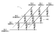
図2は、MAT1の一部の斜視図、図3は、図2におけるI−I´線で切断して矢印方向に見たメモリセル1個分の断面図である。
FIG. 2 is a perspective view of a part of the
複数本のワード線WL0〜WL2が平行に配設され、これと交差して複数本のビット線BL0〜BL2が平行に配設され、これらの各交差部に両配線に挟まれるようにメモリセルMCが配置される。ワード線WL及びビット線BLは、熱に強く、且つ抵抗値の低い材料が望ましく、例えばW、WSi、NiSi、CoSi等を用いることができる。 A plurality of word lines WL0 to WL2 are arranged in parallel, and a plurality of bit lines BL0 to BL2 are arranged in parallel to intersect with the word lines WL0 to WL2. MC is arranged. The word line WL and the bit line BL are preferably made of a material that is resistant to heat and has a low resistance value. For example, W, WSi, NiSi, CoSi, or the like can be used.
メモリセルMCは、図3に示すように、可変抵抗素子VRと非オーミック素子NOの直列接続回路からなる。 As shown in FIG. 3, the memory cell MC includes a series connection circuit of a variable resistance element VR and a non-ohmic element NO.
可変抵抗素子VRとしては、電圧印加によって、電流、熱、化学エネルギー等を介して抵抗値を変化させることができるもので、上下にバリアメタル及び接着層として機能する電極EL1、EL2が配置される。電極材としては、Pt、Au、Ag、TiAlN、SrRuO、Ru、RuN、Ir、Co、Ti、TiN、TaN、LaNiO、Al、PtIrOx、PtRhOx、Rh、TaAlN等が用いられる。また、配向性を一様にするようなメタル膜の挿入も可能である。また、別途バッファ層、バリアメタル層、接着層等を挿入することも可能である。 As the variable resistance element VR, the resistance value can be changed by applying voltage, through current, heat, chemical energy, etc., and electrodes EL1 and EL2 functioning as a barrier metal and an adhesive layer are arranged above and below. . As the electrode material, Pt, Au, Ag, TiAlN, SrRuO, Ru, RuN, Ir, Co, Ti, TiN, TaN, LaNiO, Al, PtIrOx, PtRhOx, Rh, TaAlN, or the like is used. It is also possible to insert a metal film that makes the orientation uniform. It is also possible to insert a buffer layer, a barrier metal layer, an adhesive layer, etc. separately.
可変抵抗素子VRは、カルコゲナイド等のように結晶状態と非晶質状態の相転移により抵抗値を変化させるもの(PCRAM)、金属陽イオンを析出させて電極間に架橋(コンタクティングブリッジ)を形成したり、析出した金属をイオン化したりして架橋を破壊することで抵抗値を変化させるもの(CBRAM)、一致した理論はない(抵抗変化の要因として、電極界面に存在する電荷トラップにトラップされた電荷の存在の有無により抵抗変化が起きるというもの、酸素欠損等に起因する伝導パスの存在の有無により抵抗変化が起きるというものとに、大きく2つに分かれている。)ものの電圧あるいは電流印加により抵抗値が変化するもの(ReRAM)、等を用いることができる。 The variable resistance element VR has a resistance value changed by a phase transition between a crystalline state and an amorphous state such as chalcogenide (PCRAM), and deposits metal cations to form a bridging (contacting bridge) between the electrodes. Or change the resistance value by ionizing the deposited metal to break the bridge (CBRAM), there is no consistent theory (as a factor of resistance change, trapped in the charge traps present at the electrode interface) There are two main types: the resistance change due to the presence or absence of a charge, and the resistance change depending on the presence or absence of a conduction path due to oxygen deficiency. It is possible to use the one whose resistance value changes due to (ReRAM).
図4は、ReRAMの例を示す図である。図4に示す可変抵抗素子VRは、電極層11、13の間に記録層12を配置してなる。記録層12は、少なくとも2種類の陽イオン元素を有する複合化合物から構成される。陽イオン元素の少なくとも1種類は電子が不完全に満たされたd軌道を有する遷移元素とし、且つ隣接する陽イオン元素間の最短距離は、0.32nm以下とする。具体的には、化学式AxMyXz(AとMは互いに異なる元素)で表され、例えばスピネル構造(AM2O4)、イルメナイト構造(AMO3)、デラフォサイト構造(AMO2)、LiMoN2構造(AMN2)、ウルフラマイト構造(AMO4)、オリビン構造(A2MO4)、ホランダイト構造(AxMO2)、ラムスデライト構造(AxMO2)、ぺロブスカイト構造(AMO3)等の結晶構造を持つ材料により構成される。
FIG. 4 is a diagram illustrating an example of the ReRAM. The variable resistance element VR shown in FIG. 4 has a
図4の例では、AがZn、MがMn、XがOである。記録層12内の小さな白丸は拡散イオン(Zn)、大きな白丸は陰イオン(O)、小さな黒丸は遷移元素イオン(Mn)をそれぞれ表している。記録層12の初期状態は高抵抗状態であるが、電極層11を固定電位、電極層13側に負の電圧を印加すると、記録層12中の拡散イオンの一部が電極層13側に移動し、記録層12内の拡散イオンが陰イオンに対して相対的に減少する。電極層13側に移動した拡散イオンは、電極層13から電子を受け取り、メタルとして析出するため、メタル層14を形成する。記録層12の内部では、陰イオンが過剰となり、結果的に記録層12内の遷移元素イオンの下層を上昇させる。これにより、記録層12はキャリアの注入により電子伝導性を有するようになってセット動作が完了する。再生に関しては、記録層12を構成する材料が抵抗変化を起こさない程度の微小な電流値を流せば良い。プログラム状態(低抵抗状態)を初期状態(高抵抗状態)にリセットするには、例えば記録層12に大電流を充分な時間流してジュール加熱して、記録層12の酸化還元反応を促進すれば良い。また、セット時と逆向きの電場を印加することによってもリセット動作が可能である。
In the example of FIG. 4, A is Zn, M is Mn, and X is O. Small white circles in the
非オーミック素子NOは、例えば、ショットキーダイオード、PN接合ダイオード、PINダイオード等の各種ダイオード、MIM(Metal-Insulator-Metal)構造、SIS構造(Silicon-Insulator-Silicon)等からなる。ここにもバリアメタル層、接着層を形成する電極EL2、EL3を挿入しても良い。また、ダイオードを使用する場合はその特性上、ユニポーラ動作を行うことができ、また、MIM構造、SIS構造等の場合にはバイポーラ動作を行うことが可能である。なお、非オーミック素子NOと可変抵抗素子VRの配置は、図3と上下を逆にしても良いし、非オーミック素子NOの極性を上下反転させても良い。 The non-ohmic element NO includes, for example, various diodes such as a Schottky diode, a PN junction diode, and a PIN diode, a MIM (Metal-Insulator-Metal) structure, a SIS structure (Silicon-Insulator-Silicon), and the like. Also here, electrodes EL2 and EL3 for forming a barrier metal layer and an adhesive layer may be inserted. Further, when a diode is used, a unipolar operation can be performed due to its characteristics, and a bipolar operation can be performed in the case of an MIM structure, an SIS structure, or the like. The arrangement of the non-ohmic element NO and the variable resistance element VR may be upside down with respect to FIG. 3, or the polarity of the non-ohmic element NO may be reversed upside down.
なお、以下の説明において、可変抵抗素子VRの抵抗状態が高抵抗状態にある場合をデータ“1”、低抵抗状態にある場合をデータ“0”とする。また、書き込み動作あるいはセット動作を「“0”書き込み動作」、一方、消去動作あるいはリセット動作を「“1”書き込み動作」と表現することもある。 In the following description, data “1” is set when the resistance state of the variable resistance element VR is in the high resistance state, and data “0” is set when the resistance state is in the low resistance state. Further, the write operation or set operation may be expressed as ““ 0 ”write operation”, while the erase operation or reset operation may be expressed as ““ 1 ”write operation”.
図5は、MAT1の一部を示す回路図である。 FIG. 5 is a circuit diagram showing a part of MAT1.
MAT1は、複数のワード線WLと、これら複数のワード線WLと交差する複数のビット線BLを有している。また、ワード線WL及びビット線BLの交差部には、アノードがビット線BLに接続された非オーミック素子NOであるダイオードDiと、このダイオードDiのカソード及びワード線WL間に接続された可変抵抗素子VRとからなるメモリセルMCが接続されている。MAT1のサイズは、ワード線WLやビット線BL等の電圧降下、CR遅延、データ書き込み動作の処理速度等を勘案して任意に決定することができる。 MAT1 has a plurality of word lines WL and a plurality of bit lines BL intersecting with the plurality of word lines WL. Further, at the intersection of the word line WL and the bit line BL, a diode Di which is a non-ohmic element NO whose anode is connected to the bit line BL, and a variable resistor connected between the cathode of the diode Di and the word line WL. A memory cell MC composed of the element VR is connected. The size of MAT1 can be arbitrarily determined in consideration of the voltage drop of the word line WL and the bit line BL, the CR delay, the processing speed of the data write operation, and the like.
次に、本実施形態のデータ書き込み動作について説明する。 Next, the data write operation of this embodiment will be described.
始めに、大量データを一括して取り扱うページ動作の前提として、図5中の点線で囲まれたメモリセルMC1に対する“1”書き込み動作及び“0”書き込み動作について説明する。 First, “1” write operation and “0” write operation for the memory cell MC1 surrounded by a dotted line in FIG.
図6Aは、“1”書き込み動作時におけるワード線WL及びビット線BLの動作波形である。 FIG. 6A shows operation waveforms of the word line WL and the bit line BL during the “1” write operation.
定常時において、全てのワード線WLは所定の正の電圧Va、全てのビット線BLは、接地レベルの電圧(0V)になっている。この場合、各メモリセルMCのダイオードDiには、逆方向バイアスがかかり、メモリセルMCには電圧が印加されない。 At regular times, all word lines WL are at a predetermined positive voltage Va, and all bit lines BL are at a ground level voltage (0 V). In this case, a reverse bias is applied to the diode Di of each memory cell MC, and no voltage is applied to the memory cell MC.
この状態から、所定の時間Tresetの間、メモリセルMC1に接続された選択ワード線WL1は、接地レベルの電圧(0V)に引き下げられ、続いて、選択ビット線BL1には、リセット電圧Vresetが供給される。一方、その他の非選択ワード線WL2及び非選択ビット線BL2は、定常時と同じ電圧Vaが維持される。その結果、メモリセルMC1のダイオードDiには、順方向バイアスがかかり、可変抵抗素子VRは、高抵抗状態に遷移する。一方、他のメモリセルMCには、可変抵抗素子VRの抵抗状態を遷移させるバイアスはかからない。これにより、メモリセルMC1にのみ“1”が書き込まれる。 From this state, the selected word line WL1 connected to the memory cell MC1 is pulled down to the ground level voltage (0V) for a predetermined time Treset, and then the reset voltage Vreset is supplied to the selected bit line BL1. Is done. On the other hand, other unselected word lines WL2 and unselected bit lines BL2 are maintained at the same voltage Va as in the normal state. As a result, a forward bias is applied to the diode Di of the memory cell MC1, and the variable resistance element VR transitions to a high resistance state. On the other hand, other memory cells MC are not biased to change the resistance state of the variable resistance element VR. As a result, “1” is written only in the memory cell MC1.
なお、所定の時間Tresetとして、図4の説明の通り、可変抵抗素子をジュール加熱し、酸化還元反応を生じさせるだけの十分な時間を確保する必要がある。 Note that, as the predetermined time Treset, as described in FIG. 4, it is necessary to secure a sufficient time for causing the variable resistance element to be Joule-heated to cause an oxidation-reduction reaction.
図6Bは、“0”書き込み動作時におけるワード線WL及びビット線BLの動作波形である。 FIG. 6B shows operation waveforms of the word line WL and the bit line BL during the “0” write operation.
定常時において、全てのワード線WLは所定の正の電圧Vb、全てのビット線BLは、接地レベルの電圧(0V)になっている。この場合、各メモリセルMCのダイオードDiには、逆方向バイアスがかかり、メモリセルMCには電圧が印加されない。 At regular times, all word lines WL are at a predetermined positive voltage Vb, and all bit lines BL are at a ground level voltage (0 V). In this case, a reverse bias is applied to the diode Di of each memory cell MC, and no voltage is applied to the memory cell MC.
この状態から、時間Tresetより比較的短い所定の時間Tsetの間、メモリセルMC1に接続された選択ワード線WL1は、接地レベルの電圧(0V)に引き下げられ、続いて、選択ビット線BL1には、リセット電圧Vresetより大きいセット電圧Vsetが供給される。一方、その他の非選択ワード線WL2及び非選択ビット線BL2は、定常時と同じ電圧が維持される。その結果、メモリセルMC1のダイオードDiには、順方向バイアスがかかり、可変抵抗素子VRは、低抵抗状態に遷移する。一方、他のメモリセルMCには、可変抵抗素子VRの抵抗状態を遷移させるバイアスはかからない。これにより、メモリセルMC1にのみ“0”が書き込まれる。 From this state, the selected word line WL1 connected to the memory cell MC1 is pulled down to the ground level voltage (0V) for a predetermined time Tset that is relatively shorter than the time Reset, and then, to the selected bit line BL1. A set voltage Vset larger than the reset voltage Vreset is supplied. On the other hand, the other unselected word lines WL2 and unselected bit lines BL2 are maintained at the same voltage as in the normal state. As a result, a forward bias is applied to the diode Di of the memory cell MC1, and the variable resistance element VR transitions to a low resistance state. On the other hand, other memory cells MC are not biased to change the resistance state of the variable resistance element VR. As a result, “0” is written only in the memory cell MC1.
続いて、大量データを一括して取り扱うページ動作について説明する。 Next, a page operation for handling a large amount of data at once will be described.
図7は、本実施形態におけるページの構成を示す概略図である。 FIG. 7 is a schematic diagram illustrating the configuration of a page in the present embodiment.
セルアレイは、ロウ方向にMAT(0)からMAT(n−1)まで配置され、それらn個のMATがカラム方向に配置されている。 The cell array is arranged from MAT (0) to MAT (n-1) in the row direction, and these n MATs are arranged in the column direction.
各MATが有する複数のワード線WLには、複数のメモリセルMCが接続されている。また、各MATには、上述の通り、カラム制御回路2、ロウ制御回路3及びデータラッチ4が設けられている。なお、図7では、簡単のため各MATのビット線BLは省略している。また、カラム制御回路2及びデータラッチ4は一つの構成要素として表現されている。
A plurality of memory cells MC are connected to a plurality of word lines WL included in each MAT. Each MAT is provided with the
ここで、1ページは、図7中の点線で囲まれた複数のメモリセルMCにより構成されている。つまり、MAT(0)〜MAT(n−1)が有する複数のワード線WLのうち所定の1本のワード線WLに接続された複数のメモリセルMCにより構成されている。したがって、各ワード線WLに接続されたメモリセルMC数をm個とすると1ページのメモリセル数はm×n個となる。 Here, one page is composed of a plurality of memory cells MC surrounded by dotted lines in FIG. That is, the memory cell MC is connected to a predetermined one word line WL among the plurality of word lines WL included in MAT (0) to MAT (n−1). Therefore, if the number of memory cells MC connected to each word line WL is m, the number of memory cells in one page is m × n.
データ書き込みの際には、まず、外部から与えられる1ページ分の書き込みデータが、データ入出力バッファを介して各MATのデータラッチ4に保持される。ここで、書き込みデータは、外部から与えられるページアドレスに応じて、指定されたページを構成する所定のMATのデータラッチ4へと自動的に振り分けられ転送される。続いて、各MATにおいて、データラッチ4に保持されているデータが、ページを構成する所定のメモリセルMCに書き込まれる。ここで、MAT毎に同時書き込み可能なメモリセルMCの数には制限があることから、1ページ分のデータを一時に書き込めない場合がある。しかし、この点については、データラッチ4に保持されたデータを小分けにし、同時書き込み可能な所定数のメモリセルに対して、シリアルにデータ書き込みすれば良い。このようにメモリセルMCに対する書き込みデータを複数回に分ける場合であっても、不揮発性メモリの外部からは、1ページ分の書き込みデータを分割することなく与えることができ、また、ページアドレスの指定も1回で完了することから、ページ動作をするNAND型フラッシュメモリとの互換性を確保することができる。以上により、1ページ分のデータ書き込みが完了する。
When writing data, first, write data for one page given from the outside is held in the data latch 4 of each MAT via the data input / output buffer. Here, the write data is automatically distributed and transferred to the data latch 4 of a predetermined MAT constituting the designated page in accordance with a page address given from the outside. Subsequently, in each MAT, data held in the
なお、データラッチ4は、各MAT独立に設ける必要はなく、複数のMATで共有することもできる。 The data latch 4 does not have to be provided independently for each MAT, and can be shared by a plurality of MATs.
従来あるギガビット単位の大きなセルアレイを有するNAND型フラッシュメモリの場合、1本のワード線を選択することで、それに接続された多くのメモリセルからなるページに同時にアクセスすることができる。しかし、可変抵抗素子からなるメモリセルを用いた場合、メモリセルに大電流を流すことでデータ書き換えを行う。そのため、同時にアクセスするメモリセルが多くなると、ワード線及びビット線の電圧降下により、所望のデータの書き替えができなくなるおそれがある。 In the case of a conventional NAND flash memory having a large cell array of gigabit units, by selecting one word line, it is possible to simultaneously access a page composed of many memory cells connected thereto. However, when a memory cell made of a variable resistance element is used, data is rewritten by passing a large current through the memory cell. For this reason, when the number of memory cells accessed simultaneously increases, there is a possibility that desired data cannot be rewritten due to the voltage drop of the word line and the bit line.
その点、本実施形態のように、1ページ分の書き込みデータを分割してシリアルに書き込むことによって、ワード線WL及びビット線BLによる電圧降下の影響を低減させることができる。また、セルアレイを複数のMATに分割し、複数のMATをパラレルに動作させることで、書き込み時間の高速化を図ることができる。 In this regard, as in the present embodiment, the write data for one page is divided and written serially, thereby reducing the influence of the voltage drop caused by the word line WL and the bit line BL. Further, the writing time can be increased by dividing the cell array into a plurality of MATs and operating the plurality of MATs in parallel.
次に、本実施形態のデータ読み出し動作について説明する。 Next, the data read operation of this embodiment will be described.
データ読み出し動作については、データ書き込みの場合と逆になる。つまり、各MATにおいて、ページを構成するメモリセルMCからデータラッチ4にデータが転送され、1ページ分の読み出しデータがデータラッチ4に保持される。その上で、データ入出力バッファ5に対し、データラッチ4に保持される1ページ分のデータが転送される。これら一連の動作により1ページ分のデータ読み出しが可能となる。
The data read operation is the reverse of the data write operation. That is, in each MAT, data is transferred from the memory cell MC constituting the page to the
以上から、本実施形態によれば、大量データを連続して読み書きするページ動作を実現し、NAND型フラッシュメモリの互換性を確保した可変抵抗素子を用いた不揮発性半導体記憶装置を提供することができる。 As described above, according to the present embodiment, it is possible to provide a nonvolatile semiconductor memory device using a variable resistance element that realizes a page operation for continuously reading and writing a large amount of data and ensures the compatibility of the NAND flash memory. it can.
[第2の実施形態]
図8は、本発明の第2の実施形態に係る不揮発性半導体記憶装置のページ構成を示す概略図である。なお、図8では、簡単のため各MATのビット線BLは省略している。また、カラム制御回路2及びデータラッチ4は一つの構成要素として表現されている。
[Second Embodiment]
FIG. 8 is a schematic view showing a page configuration of the nonvolatile semiconductor memory device according to the second embodiment of the present invention. In FIG. 8, the bit line BL of each MAT is omitted for simplicity. The
セルアレイは、2層の積層構造になっている。ここで、図8中の斜線で示された要素は、上層のMATとその周辺回路、その他部分は、下層のMATとその周辺回路を示す。 The cell array has a two-layer stacked structure. Here, the elements indicated by diagonal lines in FIG. 8 indicate the upper layer MAT and its peripheral circuit, and the other portions indicate the lower layer MAT and its peripheral circuit.
各層は、第1の実施形態と同様、マトリクス状に配置されたMATに分割されている。上層のロウ方向にはMAT(0)〜MAT(n−1)、下層のロウ方向にはMAT(0)´〜MAT(n−1)´がそれぞれ配置されている。1ページは、図8中の点線で示すように、MAT(0)〜MAT(n−1)及びMAT(0)´〜MAT(n−1)´が有する1本のワード線WLに接続された複数のメモリセルMCから構成されている。 Each layer is divided into MATs arranged in a matrix as in the first embodiment. MAT (0) to MAT (n−1) are arranged in the upper row direction, and MAT (0) ′ to MAT (n−1) ′ are arranged in the lower row direction. One page is connected to one word line WL included in MAT (0) to MAT (n−1) and MAT (0) ′ to MAT (n−1) ′, as indicated by a dotted line in FIG. The memory cell MC is composed of a plurality of memory cells MC.
本実施形態のように、積層構造を有するセルアレイでは、1ページを構成するメモリセルが属するMATを異なる層で構成することもでき、この場合であって、NAND型フラッシュメモリと同様のページ動作を実現することができる。 As in the present embodiment, in the cell array having a stacked structure, the MAT to which the memory cells constituting one page belong can be configured in different layers. In this case, the page operation similar to that of the NAND flash memory is performed. Can be realized.
なお、本実施形態では、2層構造のセルアレイを例として説明したが、3層以上の多層構造のセルアレイについても適用することができる。 In the present embodiment, a cell array having a two-layer structure has been described as an example, but the present invention can also be applied to a cell array having a multilayer structure of three or more layers.
[第3の実施形態]
本発明の第3の実施形態は、第2の実施形態と同様、積層構造を持つセルアレイに関する実施形態である。
[Third Embodiment]
As in the second embodiment, the third embodiment of the present invention is an embodiment related to a cell array having a stacked structure.
上述したように、各MATが備えるロウ制御回路、カラム制御回路、及びデータラッチなどの周辺回路は、最下層のMATの直下にあるSi基板上に形成されており、各層が備える配線と周辺回路とはセルアレイの積層方向に延びるコンタクトによって接続されている。そのため、上層の配線に接続されるコンタクトは、下層の配線と周辺回路とを接続するコンタクトを回避するように配設しなければならず、上層の配線をより長くする必要がある。しかし、このことにより、上層のMATはより多くのセルアレイを設けることが可能となる。 As described above, the peripheral circuits such as the row control circuit, the column control circuit, and the data latch included in each MAT are formed on the Si substrate immediately below the lowermost MAT, and the wirings and peripheral circuits included in each layer are provided. Are connected by contacts extending in the stacking direction of the cell array. Therefore, the contact connected to the upper layer wiring must be disposed so as to avoid the contact connecting the lower layer wiring and the peripheral circuit, and the upper layer wiring needs to be longer. However, this makes it possible to provide more cell arrays in the upper MAT.
本実施形態は、このようなMATの大きさが層毎に異なるセルアレイにおけるページ構成に関するものである。 The present embodiment relates to a page configuration in a cell array in which the size of the MAT is different for each layer.
図9は、本実施形態におけるページ構成を示す概略図である。なお、簡単化のためロウ制御回路、カラム制御回路、及びデータラッチは省略している。 FIG. 9 is a schematic diagram showing a page configuration in the present embodiment. For simplification, the row control circuit, the column control circuit, and the data latch are omitted.
このメモリセルアレイは、2層からなる積層構造になっている。ここで、図9中の斜線で示された要素は、上層のMAT、その他部分は、下層のMATとその周辺回路を示す。 This memory cell array has a laminated structure composed of two layers. Here, the elements indicated by diagonal lines in FIG. 9 indicate the upper layer MAT, and the other portions indicate the lower layer MAT and its peripheral circuits.
下層には、MAT(0)、MAT(1)が配置されており、上層には、これらMAT(0)、MAT(1)の真上に位置するMAT(0)´、MAT(1)´が配置されている。MAT(0)´はMAT(0)よりカラム方向に長くなっている。ここでは、MAT(0)の真上の領域をA1、その領域A1のカラム方向両端と接する領域をA2、A3とする。同様に、MAT(1)´は、MAT(1)よりカラム方向に長くなっている。ここでは、MAT(1)の真上の領域をA4、その領域A4のカラム方向両端と接する領域をA5、A6とする。 In the lower layer, MAT (0) and MAT (1) are arranged, and in the upper layer, MAT (0) ′ and MAT (1) ′ positioned immediately above these MAT (0) and MAT (1). Is arranged. MAT (0) ′ is longer in the column direction than MAT (0). Here, the area directly above MAT (0) is A1, and the areas in contact with both ends of the area A1 in the column direction are A2 and A3. Similarly, MAT (1) ′ is longer in the column direction than MAT (1). Here, the area immediately above MAT (1) is A4, and the areas in contact with both ends of the area A4 in the column direction are A5 and A6.
領域A1及びA4は、MAT(0)及びMAT(1)と同数のワード線WLを有しているため、第2の実施形態の場合と同様、領域A1のワード線WL1とMAT(0)´の所定のワード線WLに接続された複数のメモリセルによりページを構成する。この場合、上層のMAT(0)´の領域A2、A3とMAT(1)´の領域A5、A6にあるワード線WLについて、下層のMAT(0)、MAT(1)のワード線WLとの組み合わせによるページ構成を取ることができない。そこで、例えば、上層のMAT(0)´の領域A3のワード線WL3に接続されたメモリセルと、MAT(1)´の領域A5に位置するワード線WL5に接続されたメモリセルとで1ページを構成する。同様に、上層のMAT(0)´の領域A2のワード線WL2に接続されたメモリセルと、MAT(1)´の領域A6に位置するワード線WL6に接続されたメモリセルとで1ページを構成する。 Since the regions A1 and A4 have the same number of word lines WL as MAT (0) and MAT (1), the word lines WL1 and MAT (0) ′ in the region A1 are the same as in the second embodiment. A page is constituted by a plurality of memory cells connected to a predetermined word line WL. In this case, the word lines WL in the upper-layer MAT (0) ′ regions A2 and A3 and the MAT (1) ′ regions A5 and A6 are connected to the lower-layer MAT (0) and MAT (1) word lines WL. Cannot take a page structure by combination. Therefore, for example, one page of the memory cell connected to the word line WL3 in the region A3 of the upper MAT (0) ′ and the memory cell connected to the word line WL5 located in the region A5 of the MAT (1) ′. Configure. Similarly, one page is composed of a memory cell connected to the word line WL2 in the area A2 of the upper MAT (0) ′ and a memory cell connected to the word line WL6 located in the area A6 of the MAT (1) ′. Configure.
以上のように、本実施形態によれば、層毎にMATの大きさが異なるセルアレイの場合であっても、全てのメモリセルをページ単位にまとめることができるため、第1、第2の実施形態と同様に、ページ動作を実現することができる。 As described above, according to the present embodiment, even in the case of a cell array having a different MAT size for each layer, all memory cells can be grouped in page units. Similar to the form, a page operation can be realized.
なお、本実施形態では、2層構造のセルアレイを例として説明したが、3層以上の多層構造のセルアレイについても適用することができる。 In the present embodiment, a cell array having a two-layer structure has been described as an example, but the present invention can also be applied to a cell array having a multilayer structure of three or more layers.
[第4の実施形態]
図10は、本発明の第4の実施形態に係る不揮発性メモリの書き込み動作を示す概略図である。また、図11は、図10における書き込み動作のタイミングを示す図である。図11において、D[i][j][k]は、図10に示されたページiに属するMAT(j)のメモリセルMCkへの書き込みデータを示す。
[Fourth Embodiment]
FIG. 10 is a schematic view showing a write operation of the nonvolatile memory according to the fourth embodiment of the present invention. FIG. 11 is a diagram showing the timing of the write operation in FIG. In FIG. 11, D [i] [j] [k] indicates write data to the memory cell MCk of MAT (j) belonging to page i shown in FIG.
図10に示す通り、本実施形態のセルアレイは、ロウ方向にn個のMAT(0)〜MAT(n−1)が配置されている。ページは、これらMAT(0)〜MAT(n−1)のワード線WLを1本ずつ組み合わせ構成されている。例えば、ページ0は、MAT(0)〜MAT(n−1)のそれぞれが備えるワード線WL0に接続された複数のメモリセルMCにより構成されている。
As shown in FIG. 10, in the cell array of this embodiment, n MAT (0) to MAT (n-1) are arranged in the row direction. The page is configured by combining these word lines WL of MAT (0) to MAT (n−1) one by one. For example,
このような構成のセルアレイに対し、本実施形態では、データラッチ4によるデータの保持、このデータのメモリセルMCへの書き込みをパイプライン処理する。
In the present embodiment, pipeline processing is performed on the cell array having such a configuration to hold data by the
図11の時刻T0において、データ入出力バッファから各MATのデータラッチ4に対して、ページ0を構成するメモリセルMCへの書き込みデータが転送される。データ入出力バッファ5からデータラッチ4へのデータ転送は、例えば、MAT(0)のメモリセルMC0〜MCm−1に書き込むデータD[0][0][0]〜D[0][0][m−1]、MAT(1)のMC0〜MCm−1に書き込むデータD[0][1][0]〜D[0][1][m−1]というように、MAT毎に転送される。
At time T0 in FIG. 11, write data to the memory cell
続いて、時刻T1において、時刻T0でデータラッチ4に保持された書き込みデータがメモリセルMCに書き込まれる。データ書き込みの手順として、例えば、MAT(0)〜MAT(n−1)がそれぞれ有するメモリセルMC0に対し、書き込みデータD[0][0][0]〜D[0][n−1][0]がパラレルに書き込まれる。続いて、MAT(0)〜MAT(n−1)のそれぞれが有するメモリセルMC1に対し、書き込みデータD[0][0][1]〜D[0][n−1][1]がパラレルに書き込まれる。以上の動作をメモリセルMC2、・・・、MCm−1に順次繰り返すことで、1ページ分のデータ書き込みを行うことができる。 Subsequently, at time T1, the write data held in the data latch 4 at time T0 is written into the memory cell MC. As a data writing procedure, for example, write data D [0] [0] [0] to D [0] [n-1] is written to the memory cell MC0 included in each of MAT (0) to MAT (n-1). [0] is written in parallel. Subsequently, write data D [0] [0] [1] to D [0] [n−1] [1] is written to the memory cell MC1 included in each of MAT (0) to MAT (n−1). Written in parallel. Data for one page can be written by sequentially repeating the above operation to the memory cells MC2,..., MCm-1.
一方、時刻T1においては、メモリセルMCへのデータ書き込みと並行して、次のページであるページ1に書き込むデータD[1][0][0]〜D[1][0][m−1]、D[1][1][0]〜D[1][1][m−1]、・・・が各MATのデータラッチ4に転送される。
On the other hand, at time T1, in parallel with data writing to the memory cell MC, data D [1] [0] [0] to D [1] [0] [m−] to be written to
続いて、時刻T2において、時刻T1で各MATのデータラッチ4に転送されたページ1のデータが、ページ1を構成するメモリセルMCに書き込まれるのと並行して、データ入出力バッファ5から各MATのデータラッチ4に対し、次のページであるページ2に書き込まれるデータが転送される。
Subsequently, at the time T2, the data of the
以上が繰り返されることで、複数ページへのデータ書き込みが完了する。 By repeating the above, data writing to a plurality of pages is completed.
データ読み出し処理についても同様に、先ず、最初のページを構成するメモリセルMCのデータがデータラッチ4に保持される。続いて、保持されている最初のページの読み出しデータがデータ入出力バッファに転送されるとともに、次のページを構成するメモリセルMCのデータがデータラッチ4に保持される。以上が繰り返されることで複数ページのデータ読み出しが完了する。
Similarly, in the data reading process, first, data of the memory cell MC constituting the first page is held in the
本実施形態によれば、第1の実施形態の場合と同様に、NAND型フラッシュメモリなどとの互換性を確保するためのページ動作が実現できるばかりでなく、データ入出力バッファ5及びデータラッチ4間のデータ送受信と、メモリセルMC及びデータラッチ4間のデータ書き込み/読み出しをパイプライン処理することで、複数ページにわたるデータの書き込み/読み出しを高速に処理することができる。
According to the present embodiment, as in the case of the first embodiment, not only a page operation for ensuring compatibility with a NAND flash memory or the like can be realized, but also the data input /
1・・・MAT(単位セルアレイ)、2・・・カラム制御回路、3・・・ロウ制御回路、4・・・データラッチ、5・・・データ入出力バッファ、6・・・アドレスレジスタ、7・・・コマンド・インターフェイス、8・・・コントローラ、9・・・パルスジェネレータ、11、13・・・電極層、12・・・記録層、14・・・メタル層。
DESCRIPTION OF
Claims (5)
前記各MATのメモリセルに対する書き込みデータ又は前記メモリセルからの読み出しデータを保持するデータラッチと、
前記各MATのアクセスすべきメモリセルにつながる第1及び第2の配線を選択し、前記選択された第1及び第2の配線間を前記データの書き込み又は読み出しのために駆動する第1及び第2の駆動回路と
を備え、
複数のMATのそれぞれから選択された複数の第1の配線に接続される複数のメモリセルで1つのページを構成し、
前記データラッチは、前記書き込みデータ又は読み出しデータをページ単位でラッチし、
前記第1及び第2の駆動回路は、同時アクセス可能な所定数の前記メモリセルに記憶できる大きさのデータをアクセス単位データとした場合、1ページ分のデータを前記第1及び第2の配線に対する複数回の駆動によって前記アクセス単位データずつシリアルに前記セルアレイに書き込み又は前記セルアレイから読み出す
ことを特徴とする不揮発性半導体記憶装置。 A plurality of first wirings, a plurality of second wirings intersecting with the plurality of first wirings, and electrical rewriting connected between both wirings at the intersection of the first and second wirings are possible. A cell array in which a plurality of MATs (unit cell arrays) having memory cells each having a variable resistance element for storing resistance values in a nonvolatile manner as data are arranged in a matrix;
A data latch for holding write data to the memory cell of each MAT or read data from the memory cell;
First and second wirings connected to the memory cell to be accessed of each MAT are selected, and first and second wirings are driven between the selected first and second wirings for writing or reading data. Two drive circuits, and
One page is composed of a plurality of memory cells connected to a plurality of first wirings selected from each of a plurality of MATs,
The data latch latches the write data or read data in page units,
When the first and second drive circuits use data of a size that can be stored in a predetermined number of memory cells that can be accessed simultaneously as access unit data, the data for one page is transferred to the first and second wirings. A non-volatile semiconductor memory device, wherein the access unit data is serially written to or read from the cell array by a plurality of times of driving.
ことを特徴とする請求項1記載の不揮発性半導体記憶装置。 The nonvolatile semiconductor memory device according to claim 1, wherein the data latch and the first and second drive circuits are provided for each MAT.
ことを特徴とする請求項1又は2記載の不揮発性半導体記憶装置。 The nonvolatile semiconductor memory device according to claim 1, wherein a combination of the predetermined page and a MAT to which a memory cell constituting another predetermined page belongs is different.
前記ページを構成するメモリセルの属するMATと前記ページを構成する他のメモリセルの属するMATが同じ層に属する
ことを特徴とする請求項1〜3のいずれか1項記載の不揮発性半導体記憶装置。 The cell array has a laminated structure in which a plurality of layers made of a predetermined number of MATs are laminated.
4. The nonvolatile semiconductor memory device according to claim 1, wherein a MAT to which a memory cell constituting the page belongs and a MAT to which another memory cell constituting the page belongs belong to the same layer. 5. .
前記ページを構成するメモリセルの属するMATと前記ページを構成する他のメモリセルの属するMATが異なる層に属する
ことを特徴とする請求項1〜3のいずれか1項記載の不揮発性半導体記憶装置。
The cell array has a laminated structure in which a plurality of layers made of a predetermined number of MATs are laminated.
4. The nonvolatile semiconductor memory device according to claim 1, wherein a MAT to which a memory cell constituting the page belongs and a MAT to which another memory cell constituting the page belongs belong to different layers. 5. .
Priority Applications (3)
| Application Number | Priority Date | Filing Date | Title |
|---|---|---|---|
| JP2008268379A JP5178448B2 (en) | 2008-10-17 | 2008-10-17 | Nonvolatile semiconductor memory device |
| US12/580,795 US8089818B2 (en) | 2008-10-17 | 2009-10-16 | Nonvolatile semiconductor memory device |
| US13/315,967 US8427885B2 (en) | 2008-10-17 | 2011-12-09 | Nonvolatile semiconductor memory device |
Applications Claiming Priority (1)
| Application Number | Priority Date | Filing Date | Title |
|---|---|---|---|
| JP2008268379A JP5178448B2 (en) | 2008-10-17 | 2008-10-17 | Nonvolatile semiconductor memory device |
Publications (2)
| Publication Number | Publication Date |
|---|---|
| JP2010097662A JP2010097662A (en) | 2010-04-30 |
| JP5178448B2 true JP5178448B2 (en) | 2013-04-10 |
Family
ID=42108541
Family Applications (1)
| Application Number | Title | Priority Date | Filing Date |
|---|---|---|---|
| JP2008268379A Active JP5178448B2 (en) | 2008-10-17 | 2008-10-17 | Nonvolatile semiconductor memory device |
Country Status (2)
| Country | Link |
|---|---|
| US (2) | US8089818B2 (en) |
| JP (1) | JP5178448B2 (en) |
Families Citing this family (18)
| Publication number | Priority date | Publication date | Assignee | Title |
|---|---|---|---|---|
| JP5049814B2 (en) | 2008-02-14 | 2012-10-17 | 株式会社東芝 | Data writing method for nonvolatile semiconductor memory device |
| JP2010044827A (en) | 2008-08-13 | 2010-02-25 | Toshiba Corp | Nonvolatile semiconductor storage device |
| JP2010192040A (en) * | 2009-02-18 | 2010-09-02 | Toshiba Corp | Semiconductor memory device |
| JP2011040633A (en) * | 2009-08-13 | 2011-02-24 | Toshiba Corp | Semiconductor memory device |
| US8639903B2 (en) | 2010-05-13 | 2014-01-28 | Micron Technology, Inc. | Staggered programming for resistive memories |
| JP5756622B2 (en) * | 2010-11-30 | 2015-07-29 | 株式会社日立製作所 | Semiconductor device |
| JP5416079B2 (en) * | 2010-12-16 | 2014-02-12 | 株式会社日立製作所 | Semiconductor memory device and memory module |
| JP5481428B2 (en) * | 2011-05-26 | 2014-04-23 | 株式会社東芝 | Semiconductor memory device and memory system |
| US20120327714A1 (en) * | 2011-06-23 | 2012-12-27 | Macronix International Co., Ltd. | Memory Architecture of 3D Array With Diode in Memory String |
| US8773886B2 (en) * | 2011-08-19 | 2014-07-08 | Hewlett-Packard Development Company, L.P. | Memory array with co-planar waveguide based memory element selection |
| JP5620557B2 (en) * | 2013-09-30 | 2014-11-05 | 株式会社日立製作所 | Information processing system |
| KR102151176B1 (en) | 2014-08-22 | 2020-09-02 | 삼성전자 주식회사 | Resistive Memory Device and Operating Method thereof |
| KR102261817B1 (en) | 2014-12-15 | 2021-06-07 | 삼성전자주식회사 | Resistive Memory Device and Resistive Memory System including a plurality of layers and Operating Method thereof |
| JP6397773B2 (en) * | 2015-01-30 | 2018-09-26 | 東芝メモリ株式会社 | Magnetic storage device and magnetic storage method |
| JP6359491B2 (en) * | 2015-06-12 | 2018-07-18 | 東芝メモリ株式会社 | Semiconductor memory device |
| KR20180058060A (en) * | 2016-11-23 | 2018-05-31 | 에스케이하이닉스 주식회사 | Phase Change Memory Device Capable of Distributing Peak Current |
| KR20180134124A (en) * | 2017-06-08 | 2018-12-18 | 에스케이하이닉스 주식회사 | Ferroelectric Memory Device |
| KR20190139082A (en) | 2018-06-07 | 2019-12-17 | 삼성전자주식회사 | Memory device and method for equalizing bit error rates |
Family Cites Families (11)
| Publication number | Priority date | Publication date | Assignee | Title |
|---|---|---|---|---|
| JPH10177797A (en) * | 1996-12-17 | 1998-06-30 | Toshiba Corp | Semiconductor memory |
| US7095644B2 (en) | 2003-12-22 | 2006-08-22 | Unity Semiconductor Corporation | Conductive memory array having page mode and burst mode read capability |
| KR101128246B1 (en) * | 2004-05-03 | 2012-04-12 | 유니티 세미컨덕터 코포레이션 | Non-volatile programmable memory |
| US7241655B2 (en) * | 2004-08-30 | 2007-07-10 | Micron Technology, Inc. | Method of fabricating a vertical wrap-around-gate field-effect-transistor for high density, low voltage logic and memory array |
| US7212464B2 (en) * | 2004-09-17 | 2007-05-01 | Seiko Epson Corporation | Semiconductor memory device having a plurality of latch circuits coupled to each read amplifier |
| JP4606869B2 (en) * | 2004-12-24 | 2011-01-05 | ルネサスエレクトロニクス株式会社 | Semiconductor device |
| US7885102B2 (en) * | 2006-09-15 | 2011-02-08 | Renesas Electronics Corporation | Semiconductor device |
| JP4309421B2 (en) | 2006-12-25 | 2009-08-05 | エルピーダメモリ株式会社 | Semiconductor memory device and write control method thereof |
| JP2009099206A (en) | 2007-10-17 | 2009-05-07 | Toshiba Corp | Resistance change memory device |
| JP2009164480A (en) | 2008-01-09 | 2009-07-23 | Toshiba Corp | Resistance change memory device |
| JP5049814B2 (en) | 2008-02-14 | 2012-10-17 | 株式会社東芝 | Data writing method for nonvolatile semiconductor memory device |
-
2008
- 2008-10-17 JP JP2008268379A patent/JP5178448B2/en active Active
-
2009
- 2009-10-16 US US12/580,795 patent/US8089818B2/en active Active
-
2011
- 2011-12-09 US US13/315,967 patent/US8427885B2/en active Active
Also Published As
| Publication number | Publication date |
|---|---|
| US20100097832A1 (en) | 2010-04-22 |
| US8427885B2 (en) | 2013-04-23 |
| JP2010097662A (en) | 2010-04-30 |
| US20120075916A1 (en) | 2012-03-29 |
| US8089818B2 (en) | 2012-01-03 |
Similar Documents
| Publication | Publication Date | Title |
|---|---|---|
| JP5178448B2 (en) | Nonvolatile semiconductor memory device | |
| JP5268481B2 (en) | Nonvolatile semiconductor memory device | |
| JP5049814B2 (en) | Data writing method for nonvolatile semiconductor memory device | |
| JP5100554B2 (en) | Semiconductor memory device | |
| JP5049733B2 (en) | Information processing system | |
| JP4719236B2 (en) | Semiconductor memory device and semiconductor memory system | |
| JP4719233B2 (en) | Nonvolatile semiconductor memory device | |
| JP5006369B2 (en) | Nonvolatile semiconductor memory device | |
| US8045355B2 (en) | Semiconductor memory device including a reference cell | |
| KR101239582B1 (en) | Nonvolatile semiconductor memory device | |
| JP5214560B2 (en) | Nonvolatile semiconductor memory device | |
| JP5161697B2 (en) | Nonvolatile semiconductor memory device | |
| JP2010044827A (en) | Nonvolatile semiconductor storage device | |
| US8149609B2 (en) | Nonvolatile semiconductor memory device | |
| JP2012069216A (en) | Nonvolatile semiconductor memory device | |
| JP2009224610A (en) | Semiconductor memory device | |
| JP2009193626A (en) | Semiconductor memory device | |
| JP5450846B2 (en) | Nonvolatile semiconductor memory device |
Legal Events
| Date | Code | Title | Description |
|---|---|---|---|
| A621 | Written request for application examination |
Free format text: JAPANESE INTERMEDIATE CODE: A621 Effective date: 20110304 |
|
| A977 | Report on retrieval |
Free format text: JAPANESE INTERMEDIATE CODE: A971007 Effective date: 20120926 |
|
| A131 | Notification of reasons for refusal |
Free format text: JAPANESE INTERMEDIATE CODE: A131 Effective date: 20121002 |
|
| A521 | Request for written amendment filed |
Free format text: JAPANESE INTERMEDIATE CODE: A523 Effective date: 20121203 |
|
| TRDD | Decision of grant or rejection written | ||
| A01 | Written decision to grant a patent or to grant a registration (utility model) |
Free format text: JAPANESE INTERMEDIATE CODE: A01 Effective date: 20121218 |
|
| A61 | First payment of annual fees (during grant procedure) |
Free format text: JAPANESE INTERMEDIATE CODE: A61 Effective date: 20130108 |
|
| R151 | Written notification of patent or utility model registration |
Ref document number: 5178448 Country of ref document: JP Free format text: JAPANESE INTERMEDIATE CODE: R151 |
|
| FPAY | Renewal fee payment (event date is renewal date of database) |
Free format text: PAYMENT UNTIL: 20160118 Year of fee payment: 3 |
|
| S111 | Request for change of ownership or part of ownership |
Free format text: JAPANESE INTERMEDIATE CODE: R313111 |
|
| R350 | Written notification of registration of transfer |
Free format text: JAPANESE INTERMEDIATE CODE: R350 |
|
| S111 | Request for change of ownership or part of ownership |
Free format text: JAPANESE INTERMEDIATE CODE: R313111 |
|
| R350 | Written notification of registration of transfer |
Free format text: JAPANESE INTERMEDIATE CODE: R350 |