WO2014041999A1 - 色素増感太陽電池における光触媒膜の形成方法 - Google Patents
色素増感太陽電池における光触媒膜の形成方法 Download PDFInfo
- Publication number
- WO2014041999A1 WO2014041999A1 PCT/JP2013/072797 JP2013072797W WO2014041999A1 WO 2014041999 A1 WO2014041999 A1 WO 2014041999A1 JP 2013072797 W JP2013072797 W JP 2013072797W WO 2014041999 A1 WO2014041999 A1 WO 2014041999A1
- Authority
- WO
- WIPO (PCT)
- Prior art keywords
- dye
- film
- solar cell
- sensitized solar
- oxide semiconductor
- Prior art date
- Legal status (The legal status is an assumption and is not a legal conclusion. Google has not performed a legal analysis and makes no representation as to the accuracy of the status listed.)
- Ceased
Links
Images



Classifications
-
- H—ELECTRICITY
- H01—ELECTRIC ELEMENTS
- H01G—CAPACITORS; CAPACITORS, RECTIFIERS, DETECTORS, SWITCHING DEVICES, LIGHT-SENSITIVE OR TEMPERATURE-SENSITIVE DEVICES OF THE ELECTROLYTIC TYPE
- H01G9/00—Electrolytic capacitors, rectifiers, detectors, switching devices, light-sensitive or temperature-sensitive devices; Processes of their manufacture
- H01G9/20—Light-sensitive devices
- H01G9/2068—Panels or arrays of photoelectrochemical cells, e.g. photovoltaic modules based on photoelectrochemical cells
-
- H—ELECTRICITY
- H01—ELECTRIC ELEMENTS
- H01G—CAPACITORS; CAPACITORS, RECTIFIERS, DETECTORS, SWITCHING DEVICES, LIGHT-SENSITIVE OR TEMPERATURE-SENSITIVE DEVICES OF THE ELECTROLYTIC TYPE
- H01G9/00—Electrolytic capacitors, rectifiers, detectors, switching devices, light-sensitive or temperature-sensitive devices; Processes of their manufacture
- H01G9/20—Light-sensitive devices
- H01G9/2027—Light-sensitive devices comprising an oxide semiconductor electrode
- H01G9/2031—Light-sensitive devices comprising an oxide semiconductor electrode comprising titanium oxide, e.g. TiO2
-
- H—ELECTRICITY
- H01—ELECTRIC ELEMENTS
- H01G—CAPACITORS; CAPACITORS, RECTIFIERS, DETECTORS, SWITCHING DEVICES, LIGHT-SENSITIVE OR TEMPERATURE-SENSITIVE DEVICES OF THE ELECTROLYTIC TYPE
- H01G9/00—Electrolytic capacitors, rectifiers, detectors, switching devices, light-sensitive or temperature-sensitive devices; Processes of their manufacture
- H01G9/20—Light-sensitive devices
- H01G9/2059—Light-sensitive devices comprising an organic dye as the active light absorbing material, e.g. adsorbed on an electrode or dissolved in solution
-
- Y—GENERAL TAGGING OF NEW TECHNOLOGICAL DEVELOPMENTS; GENERAL TAGGING OF CROSS-SECTIONAL TECHNOLOGIES SPANNING OVER SEVERAL SECTIONS OF THE IPC; TECHNICAL SUBJECTS COVERED BY FORMER USPC CROSS-REFERENCE ART COLLECTIONS [XRACs] AND DIGESTS
- Y02—TECHNOLOGIES OR APPLICATIONS FOR MITIGATION OR ADAPTATION AGAINST CLIMATE CHANGE
- Y02E—REDUCTION OF GREENHOUSE GAS [GHG] EMISSIONS, RELATED TO ENERGY GENERATION, TRANSMISSION OR DISTRIBUTION
- Y02E10/00—Energy generation through renewable energy sources
- Y02E10/50—Photovoltaic [PV] energy
- Y02E10/542—Dye sensitized solar cells
-
- Y—GENERAL TAGGING OF NEW TECHNOLOGICAL DEVELOPMENTS; GENERAL TAGGING OF CROSS-SECTIONAL TECHNOLOGIES SPANNING OVER SEVERAL SECTIONS OF THE IPC; TECHNICAL SUBJECTS COVERED BY FORMER USPC CROSS-REFERENCE ART COLLECTIONS [XRACs] AND DIGESTS
- Y02—TECHNOLOGIES OR APPLICATIONS FOR MITIGATION OR ADAPTATION AGAINST CLIMATE CHANGE
- Y02P—CLIMATE CHANGE MITIGATION TECHNOLOGIES IN THE PRODUCTION OR PROCESSING OF GOODS
- Y02P70/00—Climate change mitigation technologies in the production process for final industrial or consumer products
- Y02P70/50—Manufacturing or production processes characterised by the final manufactured product
Definitions
- the present invention relates to a method for forming a photocatalytic film in a dye-sensitized solar cell.
- a dye-sensitized solar cell includes, as its elements, a transparent electrode in which a transparent conductive film is formed on a transparent substrate such as a glass plate, a counter electrode, and an iodine-based electrolyte disposed between these electrodes. And a photocatalyst film disposed between the electrodes and on the surface of the transparent electrode.
- a photocatalyst film a film obtained by forming an oxide semiconductor film such as titanium oxide (TiO 2 ) and adsorbing a photosensitizing dye such as ruthenium to the oxide semiconductor film is known (for example, Patent Document 1). reference).
- Such a dye-sensitized solar cell has the advantage that the design can be improved by combining the color and the pattern since the photocatalyst film is colored with the photosensitizing dye.
- the first is a dye-sensitized solar cell in which lightness and saturation are changed by reflected light from the reflection means by providing a reflection means having irregularities on the counter electrode side (see, for example, Patent Document 2). ).
- the second is a dye-sensitized solar cell in which the thickness of the oxide semiconductor film, the particle diameter of the titanium oxide fine particles, and the like are made different so as to produce shades of color (for example, see Patent Document 3).
- a partition device divided into a plurality of spaces is installed in the oxide semiconductor film, and a different dye solution is injected into each of the divided spaces to separately paint the colors of the oxide semiconductor film ( For example, see Patent Document 4).
- JP 2001-35549 A Japanese Patent No. 4936648 JP 2010-3468 A JP 2010-9769 A
- an object of the present invention is to provide a method for forming a photocatalyst film in a dye-sensitized solar cell, in which a photocatalyst film in which an oxide semiconductor film is coated in a plurality of colors can be formed in a short time.
- a method for forming a photocatalyst film in a dye-sensitized solar cell of the present invention according to claim 1 includes a transparent electrode, a counter electrode, an electrolyte disposed between these electrodes, and a gap between both electrodes.
- a method for forming a photocatalyst film in a dye-sensitized solar cell which is disposed on the transparent electrode side and comprises a photocatalyst film formed by adsorbing a dye to an oxide semiconductor film,
- a dye-inhibiting film constituting a dye-sensitized solar cell is formed, Thereafter, the dye solution is brought into contact with the oxide semiconductor film to inhibit the dye from adsorbing in the range where the dye inhibition film is formed, and the dye inhibition film in the oxide semiconductor film is formed.
- a dye is adsorbed outside the range.
- a method for forming a photocatalyst film in a dye-sensitized solar cell of the present invention according to claim 2 is the method for forming a photocatalyst film in a dye-sensitized solar cell according to claim 1, wherein a dye solution is applied to the oxide semiconductor film. Before contact A dye-inhibiting film constituting the dye-sensitized solar cell is formed in a range where the oxide semiconductor film in the transparent electrode is not disposed.
- the method for forming a photocatalyst film in the dye-sensitized solar cell of the present invention according to claim 3 is characterized in that the dye-inhibiting film in the method for forming a photocatalyst film in the dye-sensitized solar cell according to claim 1 is a dye solution. And does not elute into the electrolyte.
- membrane in the dye-sensitized solar cell of this invention which concerns on Claim 4 is a pigment
- a method of forming an inhibitory film A mask in which a desired range is hollowed is placed on the oxide semiconductor film, Thereafter, a dye-inhibiting film precursor or solution is applied to the oxide semiconductor film by a spray method, a spin coating method, a squeegee method, or a screen printing method, The applied precursor or solution is dried.
- the mask in the method for forming a photocatalyst film in the dye-sensitized solar cell according to claim 4 includes a predetermined portion and another mask. The portion that passes through the dye-inhibiting membrane precursor or solution is different in the portion.
- membrane in the dye-sensitized solar cell of this invention which concerns on Claim 6 is formed in the formation method of the photocatalyst film
- the inhibition rate at which the dye inhibition film inhibits the adsorption of the dye is different between the predetermined portion and the other portion.
- the formation method of the photocatalyst film in the dye-sensitized solar cell of this invention which concerns on Claim 7 is the dye inhibition in the formation method of the photocatalyst film in the dye-sensitized solar cell as described in any one of Claims 1 thru
- the film is a metal film, Sputtering is used as a method for forming the dye-inhibiting film.
- a photocatalyst film in which an oxide semiconductor film is coated in a plurality of colors can be formed in a short time.
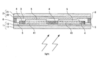
- FIG. 1 It is sectional drawing which shows schematic structure of the dye-sensitized solar cell which concerns on embodiment of this invention. It is a schematic perspective view for demonstrating a mode that a mask is arrange
- the dye-sensitized solar cell includes a transparent electrode 1 as a negative electrode, a counter electrode 2 as a positive electrode, an electrolyte layer 3 disposed between the electrodes 1 and 2, and both electrodes 1. , 2 and on the transparent electrode 1 side, a photocatalyst film (also referred to as a photocatalyst layer or a power generation layer) 4 and a sealing portion 6 that seals the outer edge between the electrodes 1 and 2 are provided. ing.
- the photocatalyst film 4 is formed by adsorbing a photosensitizing dye (not shown) to the oxide semiconductor film 41.
- the dye-inhibiting film 5 remains in the dye-sensitized solar cell in the process of forming the photocatalytic film 4 (that is, constitutes a dye-sensitized solar cell), and the photosensitizing dye is added to the oxide semiconductor film 41. It is formed to inhibit adsorption. For this reason, in the oxide semiconductor film 41, the photosensitizing dye is adsorbed in the area where the dye inhibiting film 5 is not formed to become the photocatalytic film 4, and the photosensitizing dye is formed in the area where the dye inhibiting film 5 is formed. The oxide semiconductor film 41 remains as it is not adsorbed (or a slight amount of photosensitizing dye is adsorbed).
- the oxide semiconductor film 41 is coated in a plurality of colors. Therefore, when the dye-sensitized solar cell is from the counter electrode 2 side, the color and pattern of the photocatalyst film 4 (color of the photosensitizing dye) and the dye-inhibiting film 5 (transparent or colored) can be seen. In the dye-sensitized solar cell, the color and pattern of the photocatalyst film 4 (photosensitizing dye color) and the oxide semiconductor film 41 (usually white) can be seen from the transparent electrode 1 side.
- the transparent electrode 1 includes a transparent substrate 11 and a transparent conductive film 12 formed (arranged) on the surface of the transparent substrate 11.
- the counter electrode 2 includes a transparent substrate 21 and a transparent conductive film 22 formed (arranged) on the surface of the transparent substrate 21.
- the transparent substrates 11 and 21 are not particularly limited, but although a synthetic resin plate, a glass plate, or the like is used as appropriate, it is light in weight, low in price, and safe (not easily damaged).
- a film made of a thermoplastic resin is preferred.
- the thermoplastic resin include polyester resins such as polyethylene naphthalate (PEN) and polyethylene terephthalate (PET), polycarbonate resins, and resins such as polyolefins.
- the transparent conductive films 12 and 22 are not particularly limited, but include tin-added indium oxide (ITO), fluorine-added tin oxide (FTO), tin oxide (SnO 2 ), indium zinc oxide (IZO).
- ITO tin-added indium oxide
- FTO fluorine-added tin oxide
- SnO 2 tin oxide
- IZO indium zinc oxide
- a thin film containing a conductive metal oxide such as zinc oxide (ZnO) is used.
- the transparent conductive film 22 of the counter electrode 2 is formed by forming a catalytic material.
- the counter electrode 2 is not limited to the transparent substrate 21 and the transparent conductive film 22 formed with a catalytic material, and may have any catalytic property.
- a material such as platinum or carbon having catalytic properties may be formed on a metal sheet such as aluminum, copper or tin or a mesh electrode. Examples of the method for forming the material having catalytic properties include sputtering and immersing the counter electrode 2 in a platinum nanocolloid solution.
- the counter electrode 2 has a conductive adhesive layer formed on the surface of the transparent substrate 21 on the electrolyte layer 3 side, and a vertically aligned carbon nanotube group generated separately is transferred to the conductive adhesive layer. It may be.
- an iodine electrolyte solution is used as the electrolyte layer 3.
- the electrolyte layer 3 is not limited to the electrolytic solution, and may be a solid electrolyte.
- solid electrolyte for example, is illustrated DMPImI (dimethylpropyl imidazolium iodide), but this addition, LiI, NaI, KI, CsI, metal iodide such as CaI 2, tetraalkylammonium iodide and quaternary ammonium compounds Bromide such as a combination of iodide such as iodine salt and I 2 , metal bromide such as LiBr, NaBr, KBr, CsBr and CaBr 2 , and bromide salt of quaternary ammonium compound such as tetraalkylammonium bromide and Br 2 And the like can be used as appropriate.
- DMPImI dimethylpropyl imidazolium iodide
- the photocatalytic film 4 is formed of an oxide semiconductor film 41 to which a photosensitizing dye is adsorbed.
- the oxide semiconductor include fine particles of metal oxide such as titanium oxide (TiO 2 ), tin oxide (SnO 2 ), tungsten oxide (WO 3 ), zinc oxide (ZnO), and niobium oxide (Nb 2 O 5 ). Photocatalyst fine particles) are used.
- the particle diameter of these fine particles is not particularly limited, but is preferably about 5 to 100 ⁇ m.
- photosensitizing dyes include ruthenium complexes and iron complexes having ligands containing a bipyridine structure or a terpyridine structure, porphyrin-based or phthalocyanine-based metal complexes, or organic dyes such as eosin, rhodamine, merocyanine, and coumarin. used.
- ruthenium complexes and iron complexes having ligands containing a bipyridine structure or a terpyridine structure porphyrin-based or phthalocyanine-based metal complexes, or organic dyes such as eosin, rhodamine, merocyanine, and coumarin.
- organic dyes such as eosin, rhodamine, merocyanine, and coumarin.
- titanium oxide (TiO 2 ) was used as the oxide semiconductor, it was obtained by dissolving titanium (IV) isopropoxide (TTIP) in propanol for the purpose of strengthening the bond of titanium oxide.
- a solution (which is a photocatalyst precursor solution) may be mixed with the dye solution.
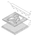
- FIG. 2 shows, as an example, a mask M for manufacturing a dye-sensitized solar cell designed as an emergency exit lamp.
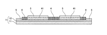
- the dye-sensitized solar cell manufactured using this mask M is formed on the oxide semiconductor film 41 of an evacuated figure and its surrounding portion (reference numeral 4 in FIG. 4) in an emergency exit lamp.
- the photosensitizing dye is adsorbed to prevent the photosensitizing dye from adsorbing to the oxide semiconductor film 41 in the portion between the human shadow and the enclosure (reference numerals 5 and 41 shown in FIG. 4). That is, as shown in FIG. 2, the mask M has an area between the human figure and the enclosure in the emergency exit lamp design. Although not shown, it is preferable to form a collector electrode on the oxide semiconductor film 41 before forming the dye inhibiting film 5 using the mask M.
- this mask M is disposed on the oxide semiconductor film 41 formed on the transparent electrode 1.
- the outer peripheral edge of the mask M and the outer peripheral edge of the oxide semiconductor film 41 are matched.
- the mask M is not covered with a range outside the outer peripheral edge of the mask M (that is, a range where the oxide semiconductor film 41 is not formed in the transparent electrode 1) and the above-described desired portion cut out in the mask M.
- the dye-inhibiting film 5 is applied to a range not covered with the mask M by a spray method in which a dye-inhibiting film solution is sprayed from above the mask M with a spray S (consisting of a main body S1 and a nozzle S2). Apply the solution.
- This coating method is not limited to the spray method described above, and an electrostatic spray method, a spin coating method, a squeegee method, a screen printing method, or the like may be used.
- the thickness of the dye inhibiting film 5 may be different between a predetermined part and another part by adjusting the number of times of application of the dye inhibiting film solution, the application pressure, the application speed, and the like.
- the dye inhibiting film 5 may have different particle diameters and polymer types between a predetermined portion and another portion. A simple way to do this is to spray the dye-inhibiting membrane solutions of different materials (solutes) with the spray S multiple times. Thus, if the thickness, the particle size, and the type of polymer of the dye inhibiting film 5 are different between the predetermined part and the other part, the dye inhibiting film 5 that the photosensitizing dye is adsorbed to the oxide semiconductor film 41 is obtained. Since the inhibition rate (hereinafter referred to as pigment inhibition rate) is different, coloring can be shaded.
- the dye inhibition film solution is obtained by dissolving the material of the dye inhibition film 5 in a solvent.
- a material that is resistant to the solvent and electrolyte of the dye solution that is, a material that does not elute into the dye solution and the electrolyte is used.
- This is a polymer (eg, polyvinyl alcohol), a metal or organic (eg, ITO) material, a resin, or a glass coating agent that does not elute into the dye solution and the electrolyte. Quartz-based, silane-based, silicon-based, or resin-based materials are used as the glass coating agent.
- membrane 5 is a metal, a metal organic compound or a metal inorganic compound etc. are used as a precursor.
- the metal organic compound include metal alkoxide, metal acetylacetonate, metal carboxylate and the like.
- Metal inorganic compounds include nitrates, oxysalt compounds, chlorides and the like. A solution in which such a precursor is dissolved in a solvent for preparing a homogeneous solution may be used.
- the dye inhibition film 5 constitutes a dye-sensitized solar cell (remains in the dye-sensitized solar cell), if the dye inhibition film 5 has conductivity, the parallel direction of the oxide semiconductor film 41 Improve the conductivity. In this case, in order to prevent a short circuit between the metal film as the dye inhibiting film 5 and the counter electrode 2, it is necessary to arrange a spacer between the both electrodes 1 and 2.
- the dye inhibiting film solution on the oxide semiconductor film 41 and the transparent electrode 1 is dried. Then, the dye inhibiting film 5 is formed in a range that is not covered with the mask M on the oxide semiconductor film 41 and the transparent electrode 1.
- membrane 5 is a metal, sputtering may be used instead of said application
- the transparent electrode 1 is immersed in a dye solution in a substantially horizontal posture, and a photosensitizing dye is brought into contact with the oxide semiconductor film 41.
- This dye solution is obtained by dissolving a photosensitizing dye in a solvent such as alcohol or acetonitrile.
- the temperature of the dye solution is from room temperature to 80 ° C., and the immersion time is about 10 to 120 minutes.
- the dye is adsorbed in the oxide semiconductor film 41 in a range where the dye inhibiting film 5 is not formed. Further, even in the range where the dye inhibiting film 5 is formed, the dye is adsorbed very slightly depending on the film thickness.
- the posture of the transparent electrode 1 immersed in the dye solution is not limited to being substantially horizontal, and may be substantially vertical or inclined.
- the method is not limited to the method of immersing the dye solution in the transparent electrode 1, but the method of dropping the dye solution onto the oxide semiconductor film 41. There may be. In this way, the photocatalyst film 4 is formed in which the desired range is not colored and the others are colored.
- a hole for injecting the electrolytic solution is formed in advance in the transparent electrode 1 or the counter electrode 2 on which the photocatalytic film 4 is formed. Then, the transparent electrode 1 and the counter electrode 2 are opposed to each other so that the photocatalytic film 4 is disposed between the electrodes 1 and 2. Next, the periphery between the electrodes 1 and 2 is sealed with a heat-sealing film or a sealant, and the electrolyte layer 3 is disposed by injecting an electrolyte solution between the electrodes 1 and 2 through the holes.
- the transparent electrode 1 and the counter electrode 2 are opposed to each other so that the photocatalyst film 4 is disposed between both the electrodes 1 and 2, and A solid electrolyte is disposed between the electrodes 1 and 2 (more precisely, between the photocatalyst film 4 and the counter electrode 2).
- the periphery of both electrodes 1 and 2 is sealed with a sealant and heat bonded.
- both the electrodes 1 and 2 are pressed with a mold and the encapsulant is heated and cured, the encapsulant is irradiated with an energy beam to cure the encapsulant, and the applied ultraviolet light
- the energy beam include plasma, visible light having a wavelength of 600 nm or more, infrared rays, and microwaves.
- the dye-inhibiting film 5 constituting the dye-sensitized solar cell is formed in the desired range of the oxide semiconductor film 41. Since the dye solution does not enter the range, and cleaning for removing the dye solution that has entered the oxide semiconductor film 41 is not necessary, the formation time of the photocatalyst film 4 can be shortened.
- the dye inhibiting film 5 constituting the dye-sensitized solar cell is formed in the transparent electrode 1 in the area where the oxide semiconductor film 41 is not disposed, the dye solution is also used in the area where the dye inhibiting film 5 is used. Therefore, it is not necessary to perform cleaning for removing the dye solution that has entered the transparent electrode 1, so that the formation time of the photocatalytic film 4 can be further shortened.
- the dye inhibiting film 5 constituting the dye-sensitized solar cell is not eluted into the dye solution, the shape of the dye inhibiting film 5 is maintained, and the oxide semiconductor film 41 can be applied beautifully. Moreover, since the pigment
- the dye inhibiting film 5 is a metal film
- the conductivity in the parallel direction of the oxide semiconductor film 41 is improved, so that the battery performance of the produced dye-sensitized solar cell can be improved.
- the oxide semiconductor film 41 formed on the transparent electrode 1 was a titanium oxide film.
- titanium oxide fine particles photocatalyst fine particles having a particle diameter of 20 nm, t-butanol, and water are mixed and stirred to produce a titanium oxide paste.
- the electrode 1 was applied and baked.
- the thickness of the titanium oxide film was 4 to 10 ⁇ m.
- a collector electrode having a thickness of about 10 ⁇ m was formed on the titanium oxide film.
- the mask M shown in FIG. 2 was placed on the titanium oxide film formed on the transparent electrode 1. At this time, the outer peripheral edge of the mask M and the outer peripheral edge of the titanium oxide film were matched. Thereafter, as shown in FIG. 3A, the dye-inhibiting film solution was applied to the area not covered with the mask M by spraying from above the mask M.
- this dye inhibiting film solution a solution in which polyvinyl alcohol was dissolved in water was used.
- the dye inhibiting film solution on the titanium oxide film and on the transparent electrode 1 was dried at about 150 ° C. Then, the pigment
- FIG. The thickness of the dye inhibiting film 5 was 10 ⁇ m (several ⁇ to several tens ⁇ m may be used).
- the transparent electrode 1 was immersed in a dye solution in a substantially horizontal posture, and a photosensitizing dye was brought into contact with the titanium oxide film.
- the squarylium dye SQ2 and the organic dye are dissolved in ethanol (an example of an alcohol), and the dye concentration is 0.1 mmol / L (it may be 0.04 to 0.5 mmol / L). It is a thing.
- the weight mixing ratio of the squarylium dye SQ2 and the organic dye is 1: 9, but the present invention is not limited to this.
- the temperature of the dye solution was arbitrarily selected from ordinary temperature to 80 ° C., and the immersion time was arbitrarily determined from 10 to 120 minutes.
- the photocatalyst film 4 in which the desired range was not colored and the others were colored was formed.
- a 100 mm square dye-sensitized solar cell was manufactured using the transparent electrode 1 on which the photocatalytic film 4 was formed.
- the dye-sensitized solar cell was irradiated with a standard light source of AM 1.5, 100 mW / cm 2 to measure the power conversion efficiency.
- the current density was 3.43 mA / cm 2
- the open-circuit voltage was 0.70 V
- the fill factor was 0.51
- the conversion efficiency was 1.22%.
- the dye-sensitized solar cell according to this example was able to prevent the battery performance from being deteriorated regardless of the element.
- each element is connected in parallel or in series to manufacture a module.
- the transparent conductive film 12, the electrolyte layer 3, the photocatalyst film 4, and the transparent conductive film 22 are partitioned by a sealing material, and the transparent conductive film 12 and the transparent conductive film 22 are separated by a conductor.
- the transparent substrate 11, the transparent conductive film 12, the transparent conductive film 22, and the transparent substrate 21 are shared.
- the material of the mask M has not been described in detail.
- a partially meshed mask M may be used. Specifically, only a predetermined part of the mask M may be meshed so that the dye-inhibiting membrane solution is slightly passed through the part. As a result, the dye inhibiting film 5 having a very small thickness is formed on the predetermined portion.
- This slight thickness of the dye-inhibiting film 5 has a low dye inhibition rate and adsorbs a slight amount of photosensitizing dye to the oxide semiconductor film 41. For this reason, the oxide semiconductor film 41 is lightly colored in the portion where the dye inhibiting film 5 having the slight thickness is formed. Therefore, by using the mask M, the pigment inhibition rate of the pigment inhibition film 5 to be formed is different between the predetermined portion and other portions, so that the coloring can be shaded.
- the mask M designed as an emergency exit lamp is used.
- this design is only an example, and other designs may of course be used.
Landscapes
- Engineering & Computer Science (AREA)
- Power Engineering (AREA)
- Chemical & Material Sciences (AREA)
- Chemical Kinetics & Catalysis (AREA)
- Electrochemistry (AREA)
- Microelectronics & Electronic Packaging (AREA)
- Hybrid Cells (AREA)
- Photovoltaic Devices (AREA)
Description
本発明は、色素増感太陽電池における光触媒膜の形成方法に関するものである。
一般に、色素増感型太陽電池は、その素子として、ガラス板などの透明基板上に透明導電膜が形成されてなる透明電極と、対向電極と、これら両電極間に配置されるヨウ素系の電解質と、上記両電極間で且つ上記透明電極の表面に配置される光触媒膜とから構成されている。また、上記光触媒膜としては、酸化チタン(TiO2)などの酸化物半導体膜を形成した後、これにルテニウムなどの光増感色素を吸着させたものが知られている(例えば、特許文献1参照)。
このような色素増感太陽電池は、光触媒膜が光増感色素により着色されているので、その色彩および模様を組み合わせることにより、デザイン性を高められるという長所がある。
そして、デザイン性を高めた色素増感太陽電池およびその製造方法の例としては、次の3つが挙げられる。第一に、凹凸が形成された反射手段を対向電極側に設けることにより、この反射手段からの反射光で明度や彩度を変化させた色素増感太陽電池である(例えば、特許文献2参照)。第二に、酸化物半導体膜の厚さや、その酸化チタン微粒子の粒径などを異なるようにして、色彩の濃淡を出すようにした色素増感太陽電池である(例えば、特許文献3参照)。第三に、複数の空間に区分けされた仕切り器具を酸化物半導体膜に設置し、区分けされた空間にそれぞれ異なる色素溶液を注入することにより、酸化物半導体膜の色を塗り分ける方法である(例えば、特許文献4参照)。
しかしながら、上記特許文献2に記載の色素増感太陽電池によると、反射光で明度や彩度が変化するものの、酸化物半導体膜の色を塗り分けることはできない。また、上記特許文献3に記載の色素増感太陽電池によると、色彩の濃淡は出せるものの、この色彩は一色のみに限定される。さらに、上記特許文献4に記載の方法によると、色を塗り分けることはできるが、酸化物半導体膜を傷つけるおそれがあるとともに、上記仕切り器具を別途製造する必要がある。
また、上記特許文献1~4に記載の色素増感太陽電池では、色を塗り分けるために色素接触防止用のマスクを用いたとしても、このマスクは色素増感太陽電池を構成せず取り外されるものであるから、マスクと酸化物半導体膜との僅かな隙間に色素が浸入することになる。このため、上記マスクを除去した後に、浸入した色素を除去するクリーニング工程が必要となり、光触媒膜の形成に時間を要するという問題があった。
そこで、本発明では、酸化物半導体膜が複数の色に塗り分けられた光触媒膜を短時間で形成することができる色素増感太陽電池における光触媒膜の形成方法を提供することを目的とする。
上記課題を解決するため、請求項1に係る本発明の色素増感太陽電池における光触媒膜の形成方法は、透明電極と、対向電極と、これら両電極間に配置される電解質と、両電極間で且つ透明電極側に配置されるとともに酸化物半導体膜に色素を吸着させてなる光触媒膜とを具備する色素増感太陽電池における光触媒膜の形成方法であって、
上記透明電極側に配置された酸化物半導体膜における所望の範囲に、色素増感太陽電池を構成する色素阻害膜を形成し、
その後、上記酸化物半導体膜に色素溶液を接触させることで、上記色素阻害膜が形成された範囲に色素が吸着することを阻害するとともに、上記酸化物半導体膜における上記色素阻害膜が形成された範囲以外に色素を吸着させるものである。
上記透明電極側に配置された酸化物半導体膜における所望の範囲に、色素増感太陽電池を構成する色素阻害膜を形成し、
その後、上記酸化物半導体膜に色素溶液を接触させることで、上記色素阻害膜が形成された範囲に色素が吸着することを阻害するとともに、上記酸化物半導体膜における上記色素阻害膜が形成された範囲以外に色素を吸着させるものである。
また、請求項2に係る本発明の色素増感太陽電池における光触媒膜の形成方法は、請求項1に記載の色素増感太陽電池における光触媒膜の形成方法において、酸化物半導体膜に色素溶液を接触させる前に、
透明電極における酸化物半導体膜が配置されていない範囲に、色素増感太陽電池を構成する色素阻害膜を形成するものである。
透明電極における酸化物半導体膜が配置されていない範囲に、色素増感太陽電池を構成する色素阻害膜を形成するものである。
さらに、請求項3に係る本発明の色素増感太陽電池における光触媒膜の形成方法は、請求項1または2に記載の色素増感太陽電池における光触媒膜の形成方法における色素阻害膜が、色素溶液および電解質に溶出しないものである。
また、請求項4に係る本発明の色素増感太陽電池における光触媒膜の形成方法は、請求項1乃至3のいずれか一項に記載の色素増感太陽電池における光触媒膜の形成方法において、色素阻害膜を形成する方法として、
所望の範囲がくり抜かれたマスクを酸化物半導体膜に配置し、
その後、色素阻害膜の前駆体または溶液を、スプレー法、スピンコート法、スキージ法、またはスクリーン印刷法により上記酸化物半導体膜に塗布し、
塗布された上記前駆体または溶液を乾燥させるものである。
所望の範囲がくり抜かれたマスクを酸化物半導体膜に配置し、
その後、色素阻害膜の前駆体または溶液を、スプレー法、スピンコート法、スキージ法、またはスクリーン印刷法により上記酸化物半導体膜に塗布し、
塗布された上記前駆体または溶液を乾燥させるものである。
また、請求項5に係る本発明の色素増感太陽電池における光触媒膜の形成方法は、請求項4に記載の色素増感太陽電池における光触媒膜の形成方法におけるマスクが、所定の部分と他の部分とで、色素阻害膜の前駆体または溶液を通過させる通過率が異なるものである。
また、請求項6に係る本発明の色素増感太陽電池における光触媒膜の形成方法は、請求項1乃至5のいずれか一項に記載の色素増感太陽電池における光触媒膜の形成方法において、形成された色素阻害膜が、所定の部分と他の部分とで、色素が吸着することを阻害する阻害率が異なるものである。
また、請求項7に係る本発明の色素増感太陽電池における光触媒膜の形成方法は、請求項1乃至3のいずれか一項に記載の色素増感太陽電池における光触媒膜の形成方法における色素阻害膜が、金属膜であり、
色素阻害膜を形成する方法として、スパッタリングが用いられたものである。
色素阻害膜を形成する方法として、スパッタリングが用いられたものである。
上記色素増感太陽電池における光触媒膜の形成方法によると、酸化物半導体膜が複数の色に塗り分けられた光触媒膜を短時間で形成することができる。
以下、本発明の実施の形態に係る色素増感太陽電池における光触媒膜の形成方法について説明する。
まず、実施の形態に係る色素増感太陽電池の概略構成を図1に基づき説明する。
この色素増感太陽電池は、図1に示すように、負極としての透明電極1と、正極としての対向電極2と、これら両電極1,2間に配置される電解質層3と、両電極1,2間で且つ透明電極1側に配置される光触媒膜(光触媒層または発電層ともいう)4と、両電極1,2間でこれらの外縁部を封止する封止部6とが具備されている。また、上記光触媒膜4は、酸化物半導体膜41に光増感色素(図示省略)を吸着させてなるものである。さらに、上記色素阻害膜5は、光触媒膜4を形成する過程で色素増感太陽電池に残存しており(つまり色素増感太陽電池を構成する)、酸化物半導体膜41に光増感色素が吸着されるのを阻害するために形成されたものである。このため、酸化物半導体膜41において、色素阻害膜5が形成されていない範囲は光増感色素が吸着されて光触媒膜4となり、色素阻害膜5が形成されている範囲は光増感色素が吸着されず(または極僅かの光増感色素が吸着されて)酸化物半導体膜41のままとなる。すなわち、上記酸化物半導体膜41は、複数の色に塗り分けられている。したがって、上記色素増感太陽電池は、対向電極2側からだと、光触媒膜4(光増感色素の色)および色素阻害膜5(透明または有色)による色彩および模様が見える。また、上記色素増感太陽電池は、透明電極1側からだと、光触媒膜4(光増感色素の色)および酸化物半導体膜41(通常は白色)の色彩および模様が見える。
上記透明電極1は、透明基板11およびこの透明基板11の表面に形成(配置)された透明導電膜12から構成されている。また対向電極2は、透明基板21およびこの透明基板21の表面に形成(配置)された透明導電膜22から構成されている。
上記各透明基板11,21としては、特に限定されるものではないが、合成樹脂板、ガラス板などが適宜使用されるものの、軽量化、低価格化および安全性(破損しにくい)の点で、熱可塑性樹脂からなるフィルムが好ましい。上記熱可塑性樹脂の例には、ポリエチレン・ナフタレート(PEN)、ポリエチレン・テレフタレート(PET)などのポリエステル樹脂、ポリカーボネート樹脂、およびポリオレフィンなどの樹脂が挙げられる。
また、透明導電膜12,22としては、特に限定されるものではないが、スズ添加酸化インジウム(ITO)、フッ素添加酸化スズ(FTO)、酸化スズ(SnO2)、インジウム亜鉛酸化物(IZO)、酸化亜鉛(ZnO)などの導電性金属酸化物を含む薄膜が使用される。なお、対向電極2の透明導電膜22は、触媒性を有する材料を形成したものである。
ところで、上記対向電極2は、上述のように、透明基板21および触媒性を有する材料を形成した透明導電膜22から構成されるものに限定されず、触媒性を有するものであればよい。この対向電極2としては、アルミニウム、銅、スズなどの金属シートやメッシュ状電極上に、触媒性を有する白金やカーボンなどの材料を形成したものであってもよい。この触媒性を有する材料を形成する方法の例には、スパッタリングや、上記対向電極2を白金ナノコロイド溶液に浸漬することなどが挙げられる。また、上記対向電極2は、透明基板21における電解質層3側の面に導電性接着剤層を形成し、別途生成された垂直配向型のカーボンナノチューブ群を、上記導電性接着剤層に転写させたものであってもよい。
上記電解質層3としては、例えば、ヨウ素系電解液が使用される。これは、ヨウ素、ヨウ化物イオン、ターシャリーブチルピリジンなどの電解質成分が、エチレンカーボネートやメトキシアセトニトリルなどの有機溶媒に溶解されたものである。なお、電解質層3は、電解液に限られるものではなく、固体電解質であってもよい。
上記固体電解質としては、例えば、DMPImI(ジメチルプロピルイミダゾリウムヨウ化物)が例示され、この他、LiI、NaI、KI、CsI、CaI2などの金属ヨウ化物、テトラアルキルアンモニウムヨーダイドなど4級アンモニウム化合物のヨウ素塩などのヨウ化物とI2とを組み合わせたもの、LiBr、NaBr、KBr、CsBr、CaBr2などの金属臭化物、およびテトラアルキルアンモニウムブロマイドなど4級アンモニウム化合物の臭素塩などの臭化物とBr2とを組み合わせたものなどを適宜使用することができる。
そして、上記光触媒膜4は、光増感色素が吸着された酸化物半導体膜41により形成されている。上記酸化物半導体としては、酸化チタン(TiO2)、酸化スズ(SnO2)、酸化タングステン(WO3)、酸化亜鉛(ZnO)、酸化ニオブ(Nb2O5)などの金属酸化物の微粒子(光触媒微粒子)が使用される。これら微粒子の粒径は、特に限定されるものではないが、5~100μm程度であることが好ましい。また、光増感色素としては、ビピリジン構造若しくはターピリジン構造を含む配位子を有するルテニウム錯体や鉄錯体、ポルフィリン系やフタロシアニン系の金属錯体、またはエオシン、ローダミン、メロシアニン、クマリンなどの有機色素などが使用される。特に、汎用性の観点からはルテニウム錯体を使用することが好ましく、有機溶媒に対する溶解性の観点からは有機色素を使用することが好ましい。また、光増感色素を溶解させる溶媒としては、エタノールなどのアルコール、アセトニトリルなどが使用される。なお、上記酸化物半導体として酸化チタン(TiO2)が使用された場合、酸化チタンの結合を強化することを目的として、チタン(IV)イソプロポキシド(TTIP)をプロパノールに溶解して得られた溶液(光触媒前駆体溶液である)を、上記色素溶液に混合してもよい。
以下、本発明の要旨である上記光触媒膜4の形成(製造)方法について説明する。
まず、所望の範囲(色素増感太陽電池および光触媒膜4の着色させたくない範囲)をくり抜いたマスクMを予め準備しておく。図2には、例として、非常口灯にデザインした色素増感太陽電池を製造するためのマスクMを示す。このマスクMを用いて製造される色素増感太陽電池は、図4に示すように、非常口灯において、避難する人影およびその囲いの部分(図4に示す符号4)の酸化物半導体膜41に光増感色素が吸着し、上記人影と囲いとの間の部分(図4に示す符号5,41)の酸化物半導体膜41に光増感色素が吸着しないようにされたものである。すなわち、このマスクMは、図2に示すように、非常口灯のデザインにおいて、上記人影と囲いとの間の範囲がくり抜かれている。なお、図示しないが、このマスクMを用いて色素阻害膜5を形成する前に、酸化物半導体膜41に集電極を形成しておくことが好ましい。
次に、このマスクMを、透明電極1に形成された酸化物半導体膜41上に配置する。このとき、マスクMの外周縁と酸化物半導体膜41の外周縁とを一致させる。これにより、マスクMで覆われないのは、マスクMの外周縁より外側の範囲(つまり透明電極1において酸化物半導体膜41が形成されていない範囲)と、マスクMにおいてくり抜かれた上記所望の範囲とである。その後、図3Aに示すように、マスクMの上から色素阻害膜溶液をスプレーS(本体S1およびノズルS2からなる)で噴霧するスプレー法により、マスクMで覆われていない範囲に色素阻害膜5溶液を塗布する。この塗布方法には、上記スプレー法に限定されず、静電スプレー法、スピンコート法、スキージ法、スクリーン印刷法などを用いてもよい。
ここで、色素阻害膜溶液の塗布回数、塗布圧および塗布速度などを調整することにより、色素阻害膜5を、所定の部分と他の部分とで、厚さが異なるようにしてもよい。また、色素阻害膜5を、所定の部分と他の部分とで、粒径および高分子の種類が異なるようにしてもよい。これらを簡単に行う方法は、材料(溶質)の異なる色素阻害膜溶液を、複数回スプレーSで噴霧することである。こうして、所定の部分と他の部分とで、色素阻害膜5の厚さ、粒径および高分子の種類が異なると、酸化物半導体膜41に光増感色素が吸着することの色素阻害膜5の阻害率(以下では色素阻害率という)が異なるので、着色に濃淡をつけることができる。
上記色素阻害膜溶液は、色素阻害膜5の材料を溶媒に溶かしたものである。この色素阻害膜5の材料としては、色素溶液の溶媒および電解質に耐性があるもの、つまり、色素溶液および電解質に溶出しないものが使用される。これは、色素溶液および電解質に溶出しない高分子(例えばポリビニルアルコール)、金属若しくは有機(例えばITO)の材料、樹脂、またはガラスコーティング剤などである。このガラスコーティング剤には、クォーツ系、シラン系、ケイ素系または樹脂系のものなどが使用される。また、色素阻害膜5の材料が金属の場合は、前駆体として金属有機化合物または金属無機化合物などが使用される。金属有機化合物には、金属アルコキシド、金属アセチルアセトネート、金属カルボキシレートなどが挙げられる。金属無機化合物には、硝酸塩、オキシ塩化合物、塩化物などが挙げられる。このような前駆体を均質溶液調整用の溶媒に溶解させた溶液が使用されることもある。なお、色素阻害膜5は、色素増感太陽電池を構成する(色素増感太陽電池に残存する)ので、色素阻害膜5が導電性を有していれば、酸化物半導体膜41の平行方向の導電性を向上させる。この場合、色素阻害膜5である金属膜と対向電極2との短絡を防止するために、スペーサを両電極1,2間に配置する必要がある。
そして、図3Bに示すように、酸化物半導体膜41からマスクMを除去した後、酸化物半導体膜41上および透明電極1上の色素阻害膜溶液を乾燥させる。すると、酸化物半導体膜41上および透明電極1上におけるマスクMで覆われていなかった範囲に、色素阻害膜5が形成される。なお、色素阻害膜5の材料が金属であれば、上記の塗布および乾燥ではなく、スパッタリングが用いられてもよい。
その後、透明電極1を略水平の姿勢まま色素溶液に浸漬して、酸化物半導体膜41に光増感色素を接触させる。この色素溶液は、光増感色素をアルコールやアセトニトリルなどの溶媒に溶かしたものである。色素溶液の温度は常温~80℃とし、浸漬する時間は10~120分程度とする。すると、図3Cに示すように、酸化物半導体膜41において、色素阻害膜5が形成されなかった範囲に、色素が吸着される。また、色素阻害膜5が形成された範囲にも、その膜厚によっては、極僅かに色素が吸着される。ここで、色素溶液に浸漬する透明電極1の姿勢は、略水平に限られず、略垂直または傾斜させてもよい。勿論、酸化物半導体膜41に光増感色素を接触させて吸着させるのであれば、透明電極1に色素溶液を浸漬する方法に限定されず、酸化物半導体膜41に色素溶液を滴下する方法であってもよい。こうして、所望の範囲が着色されず、それ以外が着色された光触媒膜4が形成される。
次に、この光触媒膜4が形成された透明電極1を使用して製造される色素増感太陽電池の製造方法について説明する。
電解質として電解液を使用する場合は、予め、光触媒膜4が形成された透明電極1または対向電極2に、電解液を注入するための孔を形成しておく。そして、両電極1,2間に光触媒膜4が配置されるようにして、透明電極1と対向電極2とを対向させて位置合わせする。次に、両電極1,2間の周囲を熱融着フィルムまたは封止剤で封止し、上記孔から両電極1,2間に電解液を注入することにより、電解質層3を配置する。
一方で、電解質として粘性の高い電解質を使用する場合は、両電極1,2間に光触媒膜4が配置されるようにして、透明電極1と対向電極2とを対向させて位置合わせするとともに、両電極1,2間(正確には光触媒膜4と対向電極2との間)に固体電解質を配置する。次に、両電極1,2の周囲を封止剤で封止して加熱接着する。この加熱接着には、金型により両電極1,2を加圧するとともに封止剤を加熱して硬化させる方法、封止剤にエネルギービームを照射して封止剤を硬化させる方法、塗布した紫外線硬化樹脂を紫外線照射により硬化させる方法などがある。なお、エネルギービームには、プラズマ、波長が600nm以上の可視光、赤外線、マイクロ波などがある。ところで、色素増感太陽電池が100mm角程度以上のように大面積である場合には、両電極1,2の短絡を防止するために、電解液にスペーサを配置することもある。
このように、上記光触媒膜4の形成方法によると、酸化物半導体膜41の所望の範囲に、色素増感太陽電池を構成する色素阻害膜5を形成したことにより、この色素阻害膜5を使用した範囲に色素溶液が浸入せず、酸化物半導体膜41上に浸入した色素溶液を除去するためのクリーニングが不要になるので、光触媒膜4の形成時間を短縮することができる。
また、透明電極1における酸化物半導体膜41が配置されていない範囲に、色素増感太陽電池を構成する色素阻害膜5を形成したことにより、この色素阻害膜5を使用した範囲にも色素溶液が浸入せず、透明電極1上に浸入した色素溶液を除去するためのクリーニングも不要になるので、光触媒膜4の形成時間を一層短縮することができる。
さらに、色素増感太陽電池を構成する色素阻害膜5が色素溶液に溶出しないで、色素阻害膜5の形状が維持されて、酸化物半導体膜41をきれいに塗り分けることができる。また、色素阻害膜5が電解質に溶出しないので、製造される色素増感太陽電池の電池性能の低下を防ぐことができる。
また、色素阻害膜5が金属膜の場合、酸化物半導体膜41の平行方向の導電性が向上するので、製造される色素増感太陽電池の電池性能を向上させることができる。
以下、上記実施の形態をより具体的に示した実施例に係る色素増感太陽電池における光触媒膜4の形成方法ついて説明する。
透明電極1に形成する酸化物半導体膜41を、酸化チタン膜とした。この酸化チタン膜を形成するのに、粒径20nmの酸化チタン微粒子(光触媒微粒子)と、t-ブタノールと、水とを混合および攪拌することにより酸化チタンペーストを生成し、この酸化チタンペーストを透明電極1に塗布および焼成した。なお、この酸化チタン膜の厚さは4~10μmとした。そして、図示しないが、酸化チタン膜に厚さが10μm程度の集電極を形成した。
次に、図2に示すマスクMを、透明電極1に形成された酸化チタン膜上に配置した。このとき、マスクMの外周縁と酸化チタン膜の外周縁とを一致させた。その後、図3Aに示すように、マスクMの上からスプレー法により、マスクMで覆われていない範囲に色素阻害膜溶液を塗布した。この色素阻害膜溶液として、ポリビニルアルコールを水に溶かしたものを使用した。
そして、図3Bに示すように、酸化チタン膜からマスクMを除去した後、酸化チタン膜上および透明電極1上の色素阻害膜溶液を150℃程度で乾燥させた。すると、酸化チタン膜上および透明電極1上におけるマスクMで覆われていなかった範囲に、色素阻害膜5が形成された。なお、この色素阻害膜5の厚さは10μm(数μ~数十μmであればよい)とした。
その後、透明電極1を略水平の姿勢のまま色素溶液に浸漬して、酸化チタン膜に光増感色素を接触させた。この色素溶液は、スクアリリウム系色素SQ2と、有機色素とをエタノール(アルコールの一例である)に溶かし、色素濃度を0.1mmol/L(0.04~0.5mmol/Lであればよい)としたものである。なお、この色素溶液において、上記スクアリリウム系色素SQ2と有機色素との重量混合比を1:9にしたが、これに限定されるものではない。色素溶液の温度は常温~80℃の任意とし、浸漬する時間は10~120分の任意とした。こうして、所望の範囲が着色されず、それ以外が着色された光触媒膜4が形成された。
次に、この光触媒膜4が形成された透明電極1を使用して、100mm角の色素増感太陽電池を製造した。この色素増感太陽電池にAM1.5,100mW/cm2の標準光源を照射して電力変換効率を計測した。その結果、電流密度が3.43mA/cm2、開放電圧が0.70V、フィルファクタが0.51、変換効率が1.22%であった。
このように、本実施例に係る光触媒膜4の形成方法によると、上記実施の形態に係る光触媒膜4の形成方法と同様の効果が得られた。
また、本実施例に係る色素増感太陽電池は、素子にもかかわらず、電池性能の低下を防止することができた。
ところで、上記実施の形態および実施例では、色素増感太陽電池の素子について説明したが、色素増感太陽電池のモジュールであってもよい。具体的には、各素子が並列または直列に接続されて、モジュールが製造される。並列に接続される場合は、隣り合う素子において、透明導電膜12、電解質層3、光触媒膜4および透明導電膜22がシール材によって仕切られるとともに、透明導電膜12と透明導電膜22が導体によって接続される。また、直列に接続される場合は、隣り合う素子において、電解質層3および光触媒膜4のみがシール材によって仕切られるとともに、透明基板11、透明導電膜12、透明導電膜22および透明基板21を共通する。
また、上記実施の形態および実施例では、マスクMの材質などについて詳しく説明しなかったが、例えば、部分的にメッシュ状にされたマスクMを用いてもよい。具体的には、マスクMにおける所定の部分のみをメッシュ状にして、その部分で色素阻害膜溶液を僅かに通過させるようにしてもよい。これにより、上記所定の部分に極僅かな厚さの色素阻害膜5が形成される。この僅かな厚さの色素阻害膜5は、色素阻害率が低く、酸化物半導体膜41に僅かな光増感色素を吸着させる。このため、上記僅かな厚さの色素阻害膜5が形成された部分では、酸化物半導体膜41が淡く着色される。したがって、上記マスクMを使用することにより、所定の部分と他の部分とで、形成される色素阻害膜5の色素阻害率が異なるので、着色に濃淡をつけることができる。
さらに、上記実施の形態および実施例では、非常口灯にデザインしたマスクMを用いたが、このデザインは一例に過ぎず、勿論、他のデザインであってもよい。
Claims (7)
- 透明電極と、対向電極と、これら両電極間に配置される電解質と、両電極間で且つ透明電極側に配置されるとともに酸化物半導体膜に色素を吸着させてなる光触媒膜とを具備する色素増感太陽電池における光触媒膜の形成方法であって、
上記透明電極側に配置された酸化物半導体膜における所望の範囲に、色素増感太陽電池を構成する色素阻害膜を形成し、
その後、上記酸化物半導体膜に色素溶液を接触させることで、上記色素阻害膜が形成された範囲に色素が吸着することを阻害するとともに、上記酸化物半導体膜における上記色素阻害膜が形成された範囲以外に色素を吸着させることを特徴とする色素増感太陽電池における光触媒膜の形成方法。 - 酸化物半導体膜に色素溶液を接触させる前に、
透明電極における酸化物半導体膜が配置されていない範囲に、色素増感太陽電池を構成する色素阻害膜を形成することを特徴とする請求項1に記載の色素増感太陽電池における光触媒膜の形成方法。 - 色素阻害膜が、色素溶液および電解質に溶出しないものであることを特徴とする請求項1または2に記載の色素増感太陽電池における光触媒膜の形成方法。
- 色素阻害膜を形成する方法として、
所望の範囲がくり抜かれたマスクを酸化物半導体膜に配置し、
その後、色素阻害膜の前駆体または溶液を、スプレー法、スピンコート法、スキージ法、またはスクリーン印刷法により上記酸化物半導体膜に塗布し、
塗布された上記前駆体または溶液を乾燥させることを特徴とする請求項1または2に記載の色素増感太陽電池における光触媒膜の形成方法。 - マスクが、所定の部分と他の部分とで、色素阻害膜の前駆体または溶液を通過させる通過率が異なるものであることを特徴とする請求項4に記載の色素増感太陽電池における光触媒膜の形成方法。
- 形成された色素阻害膜が、所定の部分と他の部分とで、色素が吸着することを阻害する阻害率が異なるものであることを特徴とする請求項1または2に記載の色素増感太陽電池における光触媒膜の形成方法。
- 色素阻害膜が、金属膜であり、
色素阻害膜を形成する方法として、スパッタリングが用いられたことを特徴とする請求項1または2に記載の色素増感太陽電池における光触媒膜の形成方法。
Applications Claiming Priority (2)
| Application Number | Priority Date | Filing Date | Title |
|---|---|---|---|
| JP2012-202144 | 2012-09-14 | ||
| JP2012202144A JP2014056779A (ja) | 2012-09-14 | 2012-09-14 | 色素増感太陽電池における光触媒膜の形成方法 |
Publications (1)
| Publication Number | Publication Date |
|---|---|
| WO2014041999A1 true WO2014041999A1 (ja) | 2014-03-20 |
Family
ID=50278121
Family Applications (1)
| Application Number | Title | Priority Date | Filing Date |
|---|---|---|---|
| PCT/JP2013/072797 Ceased WO2014041999A1 (ja) | 2012-09-14 | 2013-08-27 | 色素増感太陽電池における光触媒膜の形成方法 |
Country Status (2)
| Country | Link |
|---|---|
| JP (1) | JP2014056779A (ja) |
| WO (1) | WO2014041999A1 (ja) |
Citations (7)
| Publication number | Priority date | Publication date | Assignee | Title |
|---|---|---|---|---|
| JP2000268891A (ja) * | 1999-03-19 | 2000-09-29 | Toshiba Corp | 多色色素増感透明半導体電極部材とその製造方法、多色色素増感型太陽電池、及び表示素子 |
| JP2002064214A (ja) * | 2000-08-17 | 2002-02-28 | Honda Motor Co Ltd | 太陽電池の集電用電極およびその製造方法 |
| JP2002164563A (ja) * | 2000-09-14 | 2002-06-07 | Fuji Photo Film Co Ltd | 太陽光発電発光装置及び光電変換素子の色素増感方法 |
| JP2004039471A (ja) * | 2002-07-04 | 2004-02-05 | Sumitomo Osaka Cement Co Ltd | 色素増感型太陽電池 |
| JP2012094321A (ja) * | 2010-10-26 | 2012-05-17 | Nippon Steel Chem Co Ltd | 色素増感太陽電池のアノード極の製造方法 |
| JP2012199096A (ja) * | 2011-03-22 | 2012-10-18 | Sony Corp | 光電変換素子の製造方法および電子装置の製造方法 |
| JP2013157223A (ja) * | 2012-01-31 | 2013-08-15 | Hitachi Zosen Corp | 色素増感太陽電池用電極の製造方法 |
-
2012
- 2012-09-14 JP JP2012202144A patent/JP2014056779A/ja active Pending
-
2013
- 2013-08-27 WO PCT/JP2013/072797 patent/WO2014041999A1/ja not_active Ceased
Patent Citations (7)
| Publication number | Priority date | Publication date | Assignee | Title |
|---|---|---|---|---|
| JP2000268891A (ja) * | 1999-03-19 | 2000-09-29 | Toshiba Corp | 多色色素増感透明半導体電極部材とその製造方法、多色色素増感型太陽電池、及び表示素子 |
| JP2002064214A (ja) * | 2000-08-17 | 2002-02-28 | Honda Motor Co Ltd | 太陽電池の集電用電極およびその製造方法 |
| JP2002164563A (ja) * | 2000-09-14 | 2002-06-07 | Fuji Photo Film Co Ltd | 太陽光発電発光装置及び光電変換素子の色素増感方法 |
| JP2004039471A (ja) * | 2002-07-04 | 2004-02-05 | Sumitomo Osaka Cement Co Ltd | 色素増感型太陽電池 |
| JP2012094321A (ja) * | 2010-10-26 | 2012-05-17 | Nippon Steel Chem Co Ltd | 色素増感太陽電池のアノード極の製造方法 |
| JP2012199096A (ja) * | 2011-03-22 | 2012-10-18 | Sony Corp | 光電変換素子の製造方法および電子装置の製造方法 |
| JP2013157223A (ja) * | 2012-01-31 | 2013-08-15 | Hitachi Zosen Corp | 色素増感太陽電池用電極の製造方法 |
Also Published As
| Publication number | Publication date |
|---|---|
| JP2014056779A (ja) | 2014-03-27 |
Similar Documents
| Publication | Publication Date | Title |
|---|---|---|
| KR20100069630A (ko) | 색소 증감 광전 변환 소자 및 그 제조 방법 | |
| KR101303450B1 (ko) | 염료 감응 태양전지 및 그 제조방법 | |
| CN103168367B (zh) | 具备光散射层的染料敏化太阳能电池模组及其制造方法 | |
| KR20120136578A (ko) | 염료감응 태양전지 및 그 제조방법 | |
| KR20110086269A (ko) | 광전극의 제조 방법 및 이에 의한 광전극을 포함하는 염료감응 태양전지 | |
| US20120288977A1 (en) | Method for manufacturing dye-sensitized solar cell | |
| WO2011083689A1 (ja) | 色素増感太陽電池におけるバッファ層の形成方法 | |
| KR101409067B1 (ko) | 염료감응형 태양전지 및 그 제조방법 | |
| TW201316542A (zh) | 染料敏化太陽能電池模組及其製造方法 | |
| JP2011233376A (ja) | 色素増感太陽電池におけるバッファ層の形成方法 | |
| WO2014041999A1 (ja) | 色素増感太陽電池における光触媒膜の形成方法 | |
| KR101017805B1 (ko) | 염료 감응형 태양전지 및 그 제조방법 | |
| JP2010205581A (ja) | 導電性メッシュを用いた光電変換素子の製造方法 | |
| JP5452037B2 (ja) | 光電変換素子用電極の製造方法 | |
| JP2012156070A (ja) | 色素増感太陽電池における光触媒膜の形成方法および色素増感太陽電池 | |
| JP5511490B2 (ja) | 色素増感太陽電池における光触媒膜の形成方法 | |
| WO2011132288A1 (ja) | 光電変換素子用電極の製造方法 | |
| WO2014010393A1 (ja) | 色素増感太陽電池 | |
| JP6338458B2 (ja) | 光電変換素子、光電変換モジュールおよび光電変換素子の製造方法 | |
| JP2014063677A (ja) | 色素増感太陽電池における光触媒膜の形成方法、並びにその光触媒膜を具備した色素増感太陽電池およびその連続製造装置 | |
| JP2012212539A (ja) | 色素増感太陽電池における対向電極の製造方法および色素増感太陽電池 | |
| WO2013114983A1 (ja) | 色素増感太陽電池の製造方法 | |
| JP5376837B2 (ja) | 光電変換素子の製造方法 | |
| JP2011253741A (ja) | 半導体電極層及びその製造方法、並びに電気化学装置 | |
| KR101066511B1 (ko) | 염료 감응 태양 전지 및 그 제조 방법 |
Legal Events
| Date | Code | Title | Description |
|---|---|---|---|
| 121 | Ep: the epo has been informed by wipo that ep was designated in this application |
Ref document number: 13837425 Country of ref document: EP Kind code of ref document: A1 |
|
| NENP | Non-entry into the national phase |
Ref country code: DE |
|
| 122 | Ep: pct application non-entry in european phase |
Ref document number: 13837425 Country of ref document: EP Kind code of ref document: A1 |