WO2014038006A1 - 発光装置 - Google Patents
発光装置 Download PDFInfo
- Publication number
- WO2014038006A1 WO2014038006A1 PCT/JP2012/072556 JP2012072556W WO2014038006A1 WO 2014038006 A1 WO2014038006 A1 WO 2014038006A1 JP 2012072556 W JP2012072556 W JP 2012072556W WO 2014038006 A1 WO2014038006 A1 WO 2014038006A1
- Authority
- WO
- WIPO (PCT)
- Prior art keywords
- light emitting
- light
- emitting layer
- region
- layer group
- Prior art date
- Legal status (The legal status is an assumption and is not a legal conclusion. Google has not performed a legal analysis and makes no representation as to the accuracy of the status listed.)
- Ceased
Links
Images





Classifications
-
- H—ELECTRICITY
- H05—ELECTRIC TECHNIQUES NOT OTHERWISE PROVIDED FOR
- H05B—ELECTRIC HEATING; ELECTRIC LIGHT SOURCES NOT OTHERWISE PROVIDED FOR; CIRCUIT ARRANGEMENTS FOR ELECTRIC LIGHT SOURCES, IN GENERAL
- H05B33/00—Electroluminescent light sources
- H05B33/12—Light sources with substantially two-dimensional [2D] radiating surfaces
- H05B33/14—Light sources with substantially two-dimensional [2D] radiating surfaces characterised by the chemical or physical composition or the arrangement of the electroluminescent material, or by the simultaneous addition of the electroluminescent material in or onto the light source
-
- H—ELECTRICITY
- H05—ELECTRIC TECHNIQUES NOT OTHERWISE PROVIDED FOR
- H05B—ELECTRIC HEATING; ELECTRIC LIGHT SOURCES NOT OTHERWISE PROVIDED FOR; CIRCUIT ARRANGEMENTS FOR ELECTRIC LIGHT SOURCES, IN GENERAL
- H05B45/00—Circuit arrangements for operating light-emitting diodes [LED]
- H05B45/20—Controlling the colour of the light
-
- H—ELECTRICITY
- H05—ELECTRIC TECHNIQUES NOT OTHERWISE PROVIDED FOR
- H05B—ELECTRIC HEATING; ELECTRIC LIGHT SOURCES NOT OTHERWISE PROVIDED FOR; CIRCUIT ARRANGEMENTS FOR ELECTRIC LIGHT SOURCES, IN GENERAL
- H05B45/00—Circuit arrangements for operating light-emitting diodes [LED]
- H05B45/60—Circuit arrangements for operating LEDs comprising organic material, e.g. for operating organic light-emitting diodes [OLED] or polymer light-emitting diodes [PLED]
-
- H—ELECTRICITY
- H10—SEMICONDUCTOR DEVICES; ELECTRIC SOLID-STATE DEVICES NOT OTHERWISE PROVIDED FOR
- H10K—ORGANIC ELECTRIC SOLID-STATE DEVICES
- H10K50/00—Organic light-emitting devices
- H10K50/10—OLEDs or polymer light-emitting diodes [PLED]
- H10K50/11—OLEDs or polymer light-emitting diodes [PLED] characterised by the electroluminescent [EL] layers
- H10K50/125—OLEDs or polymer light-emitting diodes [PLED] characterised by the electroluminescent [EL] layers specially adapted for multicolour light emission, e.g. for emitting white light
-
- H—ELECTRICITY
- H10—SEMICONDUCTOR DEVICES; ELECTRIC SOLID-STATE DEVICES NOT OTHERWISE PROVIDED FOR
- H10K—ORGANIC ELECTRIC SOLID-STATE DEVICES
- H10K50/00—Organic light-emitting devices
- H10K50/10—OLEDs or polymer light-emitting diodes [PLED]
- H10K50/11—OLEDs or polymer light-emitting diodes [PLED] characterised by the electroluminescent [EL] layers
- H10K50/125—OLEDs or polymer light-emitting diodes [PLED] characterised by the electroluminescent [EL] layers specially adapted for multicolour light emission, e.g. for emitting white light
- H10K50/13—OLEDs or polymer light-emitting diodes [PLED] characterised by the electroluminescent [EL] layers specially adapted for multicolour light emission, e.g. for emitting white light comprising stacked EL layers within one EL unit
-
- H—ELECTRICITY
- H10—SEMICONDUCTOR DEVICES; ELECTRIC SOLID-STATE DEVICES NOT OTHERWISE PROVIDED FOR
- H10K—ORGANIC ELECTRIC SOLID-STATE DEVICES
- H10K59/00—Integrated devices, or assemblies of multiple devices, comprising at least one organic light-emitting element covered by group H10K50/00
- H10K59/30—Devices specially adapted for multicolour light emission
- H10K59/35—Devices specially adapted for multicolour light emission comprising red-green-blue [RGB] subpixels
- H10K59/353—Devices specially adapted for multicolour light emission comprising red-green-blue [RGB] subpixels characterised by the geometrical arrangement of the RGB subpixels
Definitions
- the present invention relates to a light emitting device.
- a light emitting element such as an organic EL (Electro-Luminescence) element
- a light source of a lighting device One of the characteristics required for such a lighting device is the emission of white light.
- a region 520 that emits red light, a region 530 that emits green light, and a region 540 that emits blue light are formed on one substrate, and these regions emit light simultaneously. It is described that white light is emitted.
- Patent Document 2 describes a lighting device having a plurality of panel-like organic light emitting sources.
- Patent Documents 3 and 4 describe that a plurality of organic EL light emitting layers are laminated between an anode and a cathode. These documents describe providing a charge generation layer between each of the plurality of organic EL light emitting layers.
- JP 2010-272886 A Japanese Patent Laid-Open No. 2004-31341 JP 2003-272860 A JP 2003-45676 A
- One of the characteristics required for a light emitting device used as illumination is to improve color rendering.
- An example of a problem to be solved by the present invention is to improve color rendering.
- the invention according to claim 1 includes a first light-emitting region having a first light-emitting layer group composed of a plurality of types of light-emitting layers that emit light having different spectral peaks.
- the first light emitting region emits a first color by causing the first light emitting layer group to emit light
- the second light emitting region is a light emitting device that emits the first color by causing the second light emitting layer group to emit light.
- FIG. It is a top view which shows description in patent document 1.
- FIG. It is a top view which shows the structure of the light-emitting device 10 which concerns on 1st Embodiment.
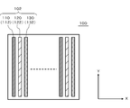
- 3 is a plan view showing a configuration of a first light emitting region 100.
- FIG. 4 is a plan view showing a configuration of a second light emitting region 200.
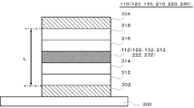
- FIG. 3 is a cross-sectional view illustrating a layer structure of a light emitting element 110.
- FIG. It is a top view which shows the modification of FIG.
- FIG. It is a top view which shows the structure of the light-emitting device 10 which concerns on 2nd Embodiment. It is a top view which shows the modification of FIG.
- FIG. 3 is a cross-sectional view illustrating a first example of a configuration of a light emitting element 140.
- FIG. 4 is a cross-sectional view illustrating a second example of the configuration of the light emitting element 140.
- the same color refers to a color included in a predetermined range in the xy chromaticity diagram, or a color having a predetermined range of color temperature, that is, a color within the same color range. It is defined as an area included in each degree.
- a predetermined range for example, a range defined by JIS can be used.
- daylight color, daylight white color, white color, warm white color, and bulb color are as defined in JISZ9112. According to this definition, the daylight color is (0.3274, 0.3673), (0.3282, 0.3297), (0.2998, 0.3396), and (0.3064) in the xy chromaticity diagram.
- 0.3091 is a region surrounded by a quadrangle, and the interphase color temperature T cp is 5700 to 7100 (K).
- lunch white is (0.3616, 0.3875), (0.3552, 0.3476), (0.3326, 0.3635), and (0.3324, 0.3296) in the xy chromaticity diagram.
- White is (0.3985, 0.4102), (0.3849, 0.3668), (0.3652, 0.3880), and (0.3584, 0.3499) in the xy chromaticity diagram.
- the interphase color temperature T cp is 3800 to 4500 (K). Also, warm white is (0.4305, 0.4218), (0.4141, 0.3834), (0.3966, 0.4044), and (0.3856, 0.3693) in the xy chromaticity diagram. ) Is a region surrounded by a quadrangle, and the interphase color temperature T cp is 3250 to 3800 (K). The light bulb colors are (0.4834, 0.4832), (0.4594, 0.3971), (0.4305, 0.4218), and (0.4153, 0.3862) in the xy chromaticity diagram. ) Is a region surrounded by a quadrangle, and the interphase color temperature T cp is 2600 to 3250 (K).
- FIG. 2 is a plan view showing the configuration of the light emitting device 10 according to the first embodiment.
- FIG. 3 is a plan view illustrating a configuration of the first light emitting region 100 included in the light emitting device 10.
- FIG. 4 is a plan view illustrating a configuration of the second light emitting region 200 included in the light emitting device 10.
- the light emitting device 10 has a first light emitting region 100 and a second light emitting region 200.
- the first light emitting region 100 has a first light emitting layer group 102.
- the first light emitting layer group 102 includes a light emitting layer 112, a light emitting layer 122, and a light emitting layer 132. These plural types of light emitting layers emit light having different spectral peaks.
- the second light emitting region 200 has a second light emitting layer group 202.
- the second light emitting layer group 202 includes a light emitting layer 212, a light emitting layer 222, and a light emitting layer 232. These plural types of light emitting layers emit light having different spectral peaks.
- the at least one light emitting layer included in the second light emitting layer group 202 emits light having a spectral peak different from any of the light emitting layers included in the first light emitting layer group 102.
- the light emitting layers constituting the first light emitting layer group 102 are different in wavelength at which the light emission intensity is maximum.
- the light emitting layers constituting the second light emitting layer group 202 are also different from each other in wavelength at which the light emission intensity is maximum.
- At least one type of light emitting layer included in the second light emitting layer group 202 is different from any light emitting layer included in the first light emitting layer group 102 in terms of the wavelength at which the light emission intensity is maximum.
- the first light emitting region 100 emits the first color by causing the first light emitting layer group 102 to emit light.
- the second light emitting region 200 also emits a first color (for example, daylight color, daylight white, white, warm white, or light bulb color) by causing the second light emitting layer group 202 to emit light.
- a first color for example, daylight color, daylight white, white, warm white, or light bulb color
- the second light emitting region 200 emits at least a light emitting layer that emits light having a spectral peak different from any of the light emitting layers of the first light emitting layer group 102. For this reason, the color rendering property of the light emitted from the light emitting device 10 is improved.
- the light emitted from the first light emitting region 100 and the light emitted from the second light emitting region 200 include different spectral peaks.
- the chromaticity of the first color emitted from the first light emitting region 100 and the chromaticity of the first color emitted from the second light emitting region 200 are located within the same color range in the xy chromaticity diagram.
- the term “in the same color range” as used herein refers to a range defined by JISZ9112, for example. For this reason, a person recognizes that they are the same color. Details will be described below.
- the first light emitting region 100 is a first light emitting panel
- the second light emitting region 200 is a second light emitting panel. That is, the first light emitting layer group 102 and the second light emitting layer group 202 are formed on different substrates.
- the first light emitting region 100 and the second light emitting region 200 are alternately arranged in both directions (X direction and Y direction in the drawing).
- the first light emitting layer group 102 has a plurality of light emitting layers formed in a stripe shape. That is, the plurality of light emitting layers constituting the first light emitting layer group 102 are formed in regions different from each other in plan view.
- the second light emitting layer group 202 has a plurality of light emitting layers formed in a stripe shape. That is, the plurality of light emitting layers constituting the second light emitting layer group 202 are formed in different regions in plan view. For this reason, it is possible to select only a desired type of light emitting layer to emit light.
- planar shape of the plurality of light emitting layers belonging to the first light emitting layer group 102 and the planar shape of the plurality of light emitting layers belonging to the second light emitting layer group 202 are both striped. For this reason, a plurality of light emitting layers can be arranged in the first light emitting region 100 with a high density, and a plurality of light emitting layers can be arranged in the second light emitting region 200 with a high density.
- the light emitting layer included in the first light emitting region 100 and the light emitting layer included in the second light emitting region 200 are, for example, organic EL light emitting layers, but may be other light emitting layers (for example, LED: Light Emitting Diode).
- the voltage or current applied to each light emitting layer is controlled by the control unit 12.
- the control unit 12 is a display driver, for example.
- the control unit 12 controls the light emission intensities of the plurality of light emitting layers included in the first light emitting layer group 102 independently of each other. Thereby, the control part 12 can change the color of the light which the 1st light emission area
- the control unit 12 can change the color of light emitted from the second light emitting region 200 by controlling the relative ratio of the light emission intensities of the plurality of light emitting layers included in the second light emitting layer group 202.
- the control unit 12 causes the light emitting layer included in the first light emitting region 100 and the light emitting layer included in the second light emitting region 200. It may be formed of a circuit that applies a predetermined voltage to each, for example, a plurality of resistance elements provided in parallel to each other.
- the first light emitting region 100 includes light emitting elements 110, 120, and 130.
- the light emitting elements 110, 120, and 130 are striped and extend in the first direction (y direction in the figure).
- the light emitting elements 110, 120, and 130 are repeatedly arranged in this order in a second direction (x direction in the figure) orthogonal to the first direction.
- the light emitting element 110 has a light emitting layer 112
- the light emitting element 120 has a light emitting layer 122
- the light emitting element 130 has a light emitting layer 132.
- the light emitting layers 112, 122, and 132 constitute the first light emitting layer group 102, and emit light of different colors.
- the combination of the colors of light emitted from the light emitting layers 112, 122, and 132 is red, green, and blue, but may be red, yellow, and blue, or magenta, yellow, and cyan. It may be red, cyan, and blue.
- the second light emitting region 200 includes light emitting elements 210, 220, and 230.
- the light emitting elements 210, 220, and 230 are striped and extend in the first direction (y direction in the figure).
- the light emitting elements 210, 220, and 230 are repeatedly arranged in this order in a second direction (x direction in the figure) orthogonal to the first direction.
- the light emitting element 210 has a light emitting layer 212
- the light emitting element 220 has a light emitting layer 222
- the light emitting element 230 has a light emitting layer 232.
- the light emitting layers 212, 222, and 232 make up the second light emitting layer group 202 and emit light of different colors.
- At least one of the light emitting layers 212, 222, and 232 emits light of a color different from any of the light emitting layers 112, 122, and 132 in the first light emitting region 100.
- the combination of colors emitted from the light emitting layers 112, 122, 132 in the first light emitting region 100 is red, green, and blue
- the combination of colors emitted from the light emitting layers 212, 222, 232 in the second light emitting region 200 is used. Are red, yellow and blue.
- both the first light emitting region 100 and the second light emitting region 200 can emit daylight color, day white color, white color, warm white color, and light bulb color.
- the combination of colors emitted by the light emitting layers 212, 222, and 232 of the second light emitting region 200 may be magenta, yellow, and cyan, or red, cyan, and blue.
- the combination of colors emitted by the light emitting layers 112, 122, and 132 in the first light emitting region 100 is red, yellow, and blue
- the combination of colors emitted by the light emitting layers 212, 222, and 232 in the second light emitting region 200 is used.
- the combination of colors emitted from the light emitting layers 112, 122, 132 in the first light emitting region 100 is magenta, yellow, and cyan
- the combination of colors emitted from the light emitting layers 212, 222, 232 in the second light emitting region 200 is used.
- the combination of colors emitted by the light emitting layers 112, 122, and 132 in the first light emitting region 100 is red, cyan, and blue
- the combination of colors emitted by the light emitting layers 212, 222, and 232 in the second light emitting region 200 is used.
- the combination of colors emitted by the light emitting layers 212, 222, and 232 of the second light emitting region 200 may be the same as the combination of colors emitted by the light emitting layers 112, 122, and 132 of the first light emitting region 100.
- at least one of the light emitting layers 212, 222, and 232 has a spectrum peak of emitted light different from that of the light emitting layers 112, 122, and 132. Even in this case, the color rendering properties of the light emitting device 10 can be improved.
- FIG. 5 is a cross-sectional view showing a layer structure of the light emitting element 110.
- the light emitting element 110 is an organic EL element.
- the light-emitting element 110 has a stacked structure in which an anode 302, a hole injection layer 312, a hole transport layer 314, a light-emitting layer 112, an electron transport layer 316, an electron injection layer 318, and a cathode 304 are stacked in this order on a substrate 300. Have.
- the light-emitting elements 120, 130, 210, 220, and 230 are organic EL elements
- the light-emitting elements are the light-emitting layer 122, the light-emitting layer 132, the light-emitting layer 212, the light-emitting layer 222, or the light-emitting layer instead of the light-emitting layer 112.
- the layer structure is similar to that of the light-emitting element 110 except that the layer 232 is formed.
- the light emitting element included in the first light emitting region 100 and the light emitting element included in the second light emitting region 200 are both organic EL elements
- the spectrum of the light emitted from each light emitting element is broadened, and the reference light of the color rendering index is displayed. Can approach the spectrum. In this case, the color rendering properties of the light emitting device 10 can be particularly increased.
- the substrate 300 is formed of a resin such as quartz, glass, metal, or plastic.
- One of the anode 302 and the cathode 304 is a transparent electrode such as ITO (Indium Tin Oxide), IZO (indium zinc oxide), and ZnO (zinc oxide), and the other is formed of a metal such as Al.
- the hole injection layer 312, the hole transport layer 314, the light emitting layer 112, the electron transport layer 316, and the electron injection layer 318 may be formed by any of a coating method and a vapor deposition method. In addition, when formed by a vapor deposition method, the following are illustrated as a material of each layer.
- Examples of phosphorescent organic compounds used in the light-emitting layer 112 include Bis ⁇ (3,5-difluoro-2- (2-pyridyl) phenyl- (2-carboxypyridyl) iridium (III), Tris (2-phenylpyridine), which are iridium complexes.
- Examples of the organic compound having an electron transporting property which is a main component of the light-emitting layer 112, the electron transport layer 316, and the electron injection layer 318 include polycyclic compounds such as p-terphenyl and quaterphenyl, and derivatives thereof, naphthalene.
- Condensed polycyclic hydrocarbon compounds such as tetracene, pyrene, coronene, chrysene, anthracene, diphenylanthracene, naphthacene, phenanthrene and their derivatives, phenanthroline, bathophenanthroline, phenanthridine, acridine, quinoline, quinoxaline, phenazine, etc.
- Ring compounds and derivatives thereof fluorescein, perylene, phthaloperylene, naphthaloperylene, perinone, phthaloperinone, naphthaloperinone, diphenylbutadiene, tetraphenylbutadiene, oxadiazole, al Examples include gin, bisbenzoxazoline, bisstyryl, pyrazine, cyclopentadiene, oxine, aminoquinoline, imine, diphenylethylene, vinylanthracene, diaminocarbazole, pyran, thiopyran, polymethine, merocyanine, quinacridone, rubrene, etc. and their derivatives. be able to.
- a metal chelate complex compound particularly a metal chelated oxanoid compound, tris (8-quinolinolato) aluminum, bis (8-quinolinolato) magnesium, bis [benzo (f) -8-quinolinolato ] Zinc, bis (2-methyl-8-quinolinolato) (4-phenyl-phenolato) aluminum, tris (8-quinolinolato) indium, tris (5-methyl-8-quinolinolato) aluminum, 8-quinolinolatolithium, tris
- metal complexes having at least one 8-quinolinolato or a derivative thereof such as (5-chloro-8-quinolinolato) gallium and bis (5-chloro-8-quinolinolato) calcium as a ligand.
- organic compounds having electron transport properties oxadiazoles, triazines, stilbene derivatives, distyrylarylene derivatives, styryl derivatives, and diolefin derivatives can be suitably used.
- organic compound that can be used as an organic compound having an electron transporting property 2,5-bis (5,7-di-t-benzyl-2-benzoxazolyl) -1,3,4-thiazole, 4, 4'-bis (5,7-t-pentyl-2-benzoxazolyl) stilbene, 4,4'-bis [5,7-di- (2-methyl-2-butyl) -2-benzoxazoly Ru] stilbene, 2,5-bis (5.7-di-t-pentyl-2-benzoxazolyl) thiophene, 2,5-bis [5- ( ⁇ , ⁇ -dimethylbenzyl) -2-benzoxa Zolyl] thiophene, 2,5-bis [5,7-di- (2-methyl-2-butyl) -2-benzoxazolyl] -3,4-diphenylthiophene, 2,5-bis (5- Methyl-2-benzoxazolyl) thiophene, 4,
- 1,4-bis (2-methylstyryl) benzene 1,4-bis (3-methylstyryl) benzene, 1,4-bis (4-methylstyryl) benzene, Distyrylbenzene, 1,4-bis (2-ethylstyryl) benzene, 1,4-bis (3-ethylstyryl) benzene, 1,4-bis (2-methylstyryl) -2-methylbenzene, 1,4 Examples thereof include -bis (2-methylstyryl) -2-ethylbenzene.
- organic compound having an electron transporting property 2,5-bis (4-methylstyryl) pyrazine, 2,5-bis (4-ethylstyryl) pyrazine, 2,5-bis [2- (1- Naphthyl) vinyl] pyrazine, 2,5-bis (4-methoxystyryl) pyrazine, 2,5-bis [2- (4-biphenyl) vinyl] pyrazine, 2,5-bis [2- (1-pyrenyl) vinyl ] Pyrazine etc. are mentioned.
- organic compounds having electron transport properties include 1,4-phenylene dimethylidin, 4,4'-phenylene dimethylidin, 2,5-xylylene dimethylidin, and 2,6-naphthylene dimethylidene. Din, 1,4-biphenylenedimethylidin, 1,4-p-terephenylenedimethylidin, 9,10-anthracenediyldimethylidin, 4,4 '-(2,2-di-t-butylphenylvinyl
- Known materials conventionally used for the production of organic EL devices such as biphenyl and 4,4 ′-(2,2-diphenylvinyl) biphenyl can be appropriately used.
- N, N, N ′, N′-tetraphenyl-4,4′-diaminophenyl is used as the hole transporting layer 314 and the hole transporting light emitting layer.
- organic compound having a hole transporting property those obtained by dispersing the above organic compound in a polymer or those obtained by polymerizing can be used.
- So-called ⁇ -conjugated polymers such as polyparaphenylene vinylene and derivatives thereof, hole-transporting non-conjugated polymers typified by poly (N-vinylcarbazole), and sigma-conjugated polymers of polysilanes can also be used.
- the hole injection layer 312 is not particularly limited, and conductive polymers such as metal phthalocyanines such as copper phthalocyanine (CuPc) and metal-free phthalocyanines, carbon films, and polyaniline can be preferably used.
- metal phthalocyanines such as copper phthalocyanine (CuPc) and metal-free phthalocyanines, carbon films, and polyaniline
- carbon films, and polyaniline can be preferably used.
- the spectral peaks of the light emitting element 110 emits light, for example by changing the material and thickness of the light-emitting layer 112 can be changed, also changing the thickness t 1 of between anode 302 and cathode 304 Also, the spectral peak of the light emitted from the light emitting element 110 can be changed. The same applies to the light emitting elements 120, 130, 210, 220, and 230.
- the light emitting device 10 has the first light emitting region 100 and the second light emitting region 200. Both the first light emitting area 100 and the second light emitting area 200 can emit light of the same color. At least one of the light emitting layers 212, 222, and 232 included in the second light emitting region 200 emits light having a spectral peak different from any of the light emitting layers 112, 122, and 132 included in the first light emitting region 100. Therefore, the color rendering property of the light emitted from the light emitting device 10 is improved.
- the light emitting elements 110, 120, 130, 210, 220, and 230 are striped.
- the arrangement interval of the same light emitting elements (for example, the arrangement interval of the light emitting elements 110) becomes wider than the resolution of the human eye, and the light emitting device 10 emits light.
- the light may not appear white.
- the light emitting elements 110, 120, and 130 are formed in the first light emitting region 100, and the light emitting elements 210, 220, and 230 are disposed in the second light emitting region 200. Can be suppressed.
- region 200 is not limited to the example shown in FIG.
- the first light emitting regions 100 and the second light emitting regions 200 may be alternately arranged in one direction (Y direction in the figure).
- FIG. 7 is a plan view showing the configuration of the light emitting device 10 according to the second embodiment.
- the light emitting device 10 according to the present embodiment has the same configuration as the light emitting device 10 according to the first embodiment, except that the substrate 300 of the first light emitting region 100 and the substrate 300 of the second light emitting region 200 are integrated. It is.
- the light emitting elements 110, 120, and 130 shown in FIG. 3 are repeatedly arranged in the region to be the first light emitting region 100 in the substrate 300. Further, the light emitting elements 210, 220, and 230 shown in FIG. 4 are repeatedly arranged in the region to be the second light emitting region 200 in the substrate 300.
- the first light emitting region 100 and the second light emitting region 200 may be arranged so that the second light emitting region 200 surrounds the first light emitting region 100.
- the same effect as that of the first embodiment can be obtained.
- the first light emitting region 100 and the second light emitting region 200 are formed on one substrate 300, labor for installing the light emitting device 10 at a desired position is reduced.
- the light emitting device 10 according to the third embodiment is the same as the light emitting device 10 according to the first embodiment except for the layout of the light emitting layer included in the first light emitting region 100 and the layout of the light emitting layer included in the second light emitting region 200. It is the structure similar to.
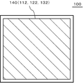
- FIG. 9 is a plan view of the first light emitting region 100 according to the present embodiment.
- the first light emitting region 100 has the light emitting element 140 on almost the entire surface of the substrate 300.
- the light emitting element 140 has a configuration in which the light emitting layers 112, 122, and 132 are stacked. That is, the light emitted from the light emitting layer 112, the light emitted from the light emitting layer 122, and the light emitted from the light emitting layer 132 are emitted from the light emitting element 140 in an overlapping manner.
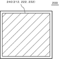
- FIG. 10 is a plan view of the second light emitting region 200 according to the present embodiment.
- the second light emitting region 200 has a light emitting element 240 on almost the entire surface of the substrate 300.
- the light emitting element 240 has a structure in which light emitting layers 212, 222, and 232 are stacked. That is, the light emitted from the light emitting layer 212, the light emitted from the light emitting layer 222, and the light emitted from the light emitting layer 232 are emitted from the light emitting element 240 in an overlapping manner.
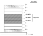
- FIG. 11 is a cross-sectional view illustrating a first example of the configuration of the light emitting element 140.
- the light-emitting element 140 includes an anode 302, a hole injection layer 312, a hole transport layer 314, a light-emitting layer 112, a light-emitting layer 122, a light-emitting layer 132, an electron transport layer 316, an electron injection layer 318, and a cathode 304 over a substrate 300.
- stacked these in this order is shown. That is, between the anode 302 and the cathode 304, the light emitting layers 112, 122, and 132 are formed so as to overlap each other.
- the light emitting layers 112, 122, 132 are arranged in series with each other.
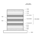
- FIG. 12 is a cross-sectional view illustrating a second example of the configuration of the light emitting element 140.
- a charge generation layer 150 is provided between the light-emitting layer 112 and the light-emitting layer 122, except that a charge generation layer 152 is provided between the light-emitting layer 122 and the light-emitting layer 132.
- the configuration is the same as that of the first example shown in FIG.
- materials described in Patent Document 3 can be used.
- the materials, film thicknesses, and the like of the light emitting layers 112, 122, and 132 are adjusted so that the first color light is emitted from the first light emitting region 100.
- the structure of the light emitting element 240 is the same as that of the light emitting element 140 shown in FIG. 11 or 12 except that the light emitting layers 212, 222, and 232 are provided instead of the light emitting layers 112, 122, and 132. It is. The material, film thickness, and the like of the light emitting layers 212, 222, and 232 are adjusted so that the first color light is emitted from the second light emitting region 200.
- the light emitting element 140 and the light emitting element 240 may be formed in different regions of the same substrate 300 as in the light emitting device 10 according to the second embodiment.
- the same effect as that of the first embodiment can be obtained.
- the light emitted from the light emitting layer 112, the light emitted from the light emitting layer 122, and the light emitted from the light emitting layer 132 are emitted from the first light emitting region 100, and the light emitting layer 212 is emitted from the second light emitting region 200.
- the light emitted from the light emitting layer 222, the light emitted from the light emitting layer 222, and the light emitted from the light emitting layer 232 are overlapped and emitted. For this reason, even if it approaches the light-emitting device 10, both the light which the 1st light emission area
Landscapes
- Physics & Mathematics (AREA)
- Optics & Photonics (AREA)
- Electroluminescent Light Sources (AREA)
Description
互いに異なるスペクトルピークの光を発光する複数種類の発光層で構成される第2発光層群を有する第2発光領域と、
を備え、
前記第2発光層群の少なくとも1種類の前記発光層は、前記第1発光層群のいずれの発光層とも異なるスペクトルピークの光を発光し、
前記第1発光領域は、前記第1発光層群を発光させることにより第1の色を発光し、
前記第2発光領域は、前記第2発光層群を発光させることにより前記第1の色を発光する発光装置である。
図2は、第1の実施形態に係る発光装置10の構成を示す平面図である。図3は、発光装置10が有する第1発光領域100の構成を示す平面図である。図4は、発光装置10が有する第2発光領域200の構成を示す平面図である。
図7は、第2の実施形態に係る発光装置10の構成を示す平面図である。本実施形態に係る発光装置10は、第1発光領域100の基板300及び第2発光領域200の基板300が一体である点を除いて、第1の実施形態に係る発光装置10と同様の構成である。
第3の実施形態に係る発光装置10は、第1発光領域100が有する発光層のレイアウト、及び第2発光領域200が有する発光層のレイアウトを除いて、第1の実施形態に係る発光装置10と同様の構成である。
Claims (8)
- 互いに異なるスペクトルピークの光を発光する複数種類の発光層で構成される第1発光層群を有する第1発光領域と、
互いに異なるスペクトルピークの光を発光する複数種類の発光層で構成される第2発光層群を有する第2発光領域と、
を備え、
前記第2発光層群の少なくとも1種類の発光層は、前記第1発光層群のいずれの発光層とも異なるスペクトルピークの光を発光し、
前記第1発光領域は、前記第1発光層群を発光させることにより第1の色を発光し、
前記第2発光領域は、前記第2発光層群を発光させることにより前記第1の色を発光する発光装置。 - 請求項1に記載の発光装置において、
xy色度図において、前記第1発光領域が発光する前記第1の色と、前記第2発光領域が発光する前記第1の色は、同一色の色度の範囲内に含まれる発光装置。 - ストライプ状に形成された複数の発光層によりなる第1発光層群と、
ストライプ状に形成された複数の発光層によりなる第2発光層群とにより構成されている請求項2に記載の発光装置。 - 前記第1発光層群は、赤色を発光する発光層、緑色を発光する発光層、及び青色を発光する発光層を含んでおり、
前記第2発光層群は、赤色を発光する発光層、黄色を発光する発光層、及び青色を発光する発光層を含んでいる請求項3に記載の発光装置。 - 前記第1発光層群及び前記第2発光層群に加える電流値または電圧を制御することにより、前記第1発光領域及び前記第2発光領域から前記第1の色を発光させる制御部を備える請求項4に記載の発光装置。
- 互いに重なって形成された複数の発光層によりなる前記第1発光層群と、
互いに重なって形成された複数の発光層によりなる前記第2発光層群とを含む請求項2に記載の発光装置。 - 前記第1発光層群は、赤色を発光する発光層、緑色を発光する発光層、及び青色を発光する発光層を含んでおり、
前記第2発光層群は、赤色を発光する発光層、黄色を発光する発光層、及び青色を発光する発光層を含んでいる請求項6に記載の発光装置。 - 前記第1発光層群及び前記第2発光層群に加える電流値または電圧を制御することにより、前記第1発光領域及び前記第2発光領域から前記第1の色を発光させる制御部を備える請求項7に記載の発光装置。
Priority Applications (4)
| Application Number | Priority Date | Filing Date | Title |
|---|---|---|---|
| JP2014534075A JP6014675B2 (ja) | 2012-09-05 | 2012-09-05 | 発光装置 |
| US14/426,121 US9420662B2 (en) | 2012-09-05 | 2012-09-05 | Light-emitting device |
| PCT/JP2012/072556 WO2014038006A1 (ja) | 2012-09-05 | 2012-09-05 | 発光装置 |
| US15/204,211 US9936559B2 (en) | 2012-09-05 | 2016-07-07 | Light-emitting device |
Applications Claiming Priority (1)
| Application Number | Priority Date | Filing Date | Title |
|---|---|---|---|
| PCT/JP2012/072556 WO2014038006A1 (ja) | 2012-09-05 | 2012-09-05 | 発光装置 |
Related Child Applications (2)
| Application Number | Title | Priority Date | Filing Date |
|---|---|---|---|
| US14/426,121 A-371-Of-International US9420662B2 (en) | 2012-09-05 | 2012-09-05 | Light-emitting device |
| US15/204,211 Continuation US9936559B2 (en) | 2012-09-05 | 2016-07-07 | Light-emitting device |
Publications (1)
| Publication Number | Publication Date |
|---|---|
| WO2014038006A1 true WO2014038006A1 (ja) | 2014-03-13 |
Family
ID=50236659
Family Applications (1)
| Application Number | Title | Priority Date | Filing Date |
|---|---|---|---|
| PCT/JP2012/072556 Ceased WO2014038006A1 (ja) | 2012-09-05 | 2012-09-05 | 発光装置 |
Country Status (3)
| Country | Link |
|---|---|
| US (2) | US9420662B2 (ja) |
| JP (1) | JP6014675B2 (ja) |
| WO (1) | WO2014038006A1 (ja) |
Families Citing this family (3)
| Publication number | Priority date | Publication date | Assignee | Title |
|---|---|---|---|---|
| US9420662B2 (en) * | 2012-09-05 | 2016-08-16 | Pioneer Corporation | Light-emitting device |
| US9577221B2 (en) * | 2012-09-26 | 2017-02-21 | Universal Display Corporation | Three stack hybrid white OLED for enhanced efficiency and lifetime |
| CN104885141B (zh) * | 2013-11-04 | 2018-03-16 | 深圳云英谷科技有限公司 | 显示器子像素排布及其渲染方法 |
Citations (5)
| Publication number | Priority date | Publication date | Assignee | Title |
|---|---|---|---|---|
| JP2007141822A (ja) * | 2005-10-17 | 2007-06-07 | Semiconductor Energy Lab Co Ltd | 照明装置 |
| JP2008511100A (ja) * | 2004-08-20 | 2008-04-10 | イーストマン コダック カンパニー | 複数の白色エレクトロルミネッセンス・ユニットを備える白色oled |
| JP2008159577A (ja) * | 2006-11-30 | 2008-07-10 | Semiconductor Energy Lab Co Ltd | 発光素子およびその発光素子を用いた発光装置 |
| JP2009224274A (ja) * | 2008-03-18 | 2009-10-01 | Panasonic Electric Works Co Ltd | 有機エレクトロルミネッセンス素子及び照明装置 |
| JP2010272886A (ja) * | 2002-08-16 | 2010-12-02 | Universal Display Corp | 照明用の有機発光デバイス |
Family Cites Families (11)
| Publication number | Priority date | Publication date | Assignee | Title |
|---|---|---|---|---|
| JP2001313172A (ja) | 2000-02-25 | 2001-11-09 | Seiko Epson Corp | 有機エレクトロルミネッセンス白色光源、及びその製造方法 |
| JP4611578B2 (ja) | 2001-07-26 | 2011-01-12 | 淳二 城戸 | 有機エレクトロルミネッセント素子 |
| JP3933591B2 (ja) | 2002-03-26 | 2007-06-20 | 淳二 城戸 | 有機エレクトロルミネッセント素子 |
| US6565231B1 (en) | 2002-05-28 | 2003-05-20 | Eastman Kodak Company | OLED area illumination lighting apparatus |
| JP2007059272A (ja) | 2005-08-25 | 2007-03-08 | Omron Corp | 照明装置及び照明方法 |
| EP1784055A3 (en) | 2005-10-17 | 2009-08-05 | Semiconductor Energy Laboratory Co., Ltd. | Lighting system |
| US8118441B2 (en) * | 2007-04-16 | 2012-02-21 | Goodrich Lighting Systems Gmbh | Color-variable LED light, particularly for lighting the interior of vehicles |
| WO2012128117A1 (ja) * | 2011-03-24 | 2012-09-27 | パナソニック株式会社 | 有機エレクトロルミネッセンス素子、照明器具、及び食品保管装置 |
| JP5699282B2 (ja) * | 2011-03-24 | 2015-04-08 | パナソニックIpマネジメント株式会社 | 有機エレクトロルミネッセンス素子及び照明器具 |
| JP5167381B2 (ja) * | 2011-03-24 | 2013-03-21 | パナソニック株式会社 | 有機エレクトロルミネッセンス素子 |
| US9420662B2 (en) * | 2012-09-05 | 2016-08-16 | Pioneer Corporation | Light-emitting device |
-
2012
- 2012-09-05 US US14/426,121 patent/US9420662B2/en active Active
- 2012-09-05 JP JP2014534075A patent/JP6014675B2/ja active Active
- 2012-09-05 WO PCT/JP2012/072556 patent/WO2014038006A1/ja not_active Ceased
-
2016
- 2016-07-07 US US15/204,211 patent/US9936559B2/en active Active
Patent Citations (5)
| Publication number | Priority date | Publication date | Assignee | Title |
|---|---|---|---|---|
| JP2010272886A (ja) * | 2002-08-16 | 2010-12-02 | Universal Display Corp | 照明用の有機発光デバイス |
| JP2008511100A (ja) * | 2004-08-20 | 2008-04-10 | イーストマン コダック カンパニー | 複数の白色エレクトロルミネッセンス・ユニットを備える白色oled |
| JP2007141822A (ja) * | 2005-10-17 | 2007-06-07 | Semiconductor Energy Lab Co Ltd | 照明装置 |
| JP2008159577A (ja) * | 2006-11-30 | 2008-07-10 | Semiconductor Energy Lab Co Ltd | 発光素子およびその発光素子を用いた発光装置 |
| JP2009224274A (ja) * | 2008-03-18 | 2009-10-01 | Panasonic Electric Works Co Ltd | 有機エレクトロルミネッセンス素子及び照明装置 |
Also Published As
| Publication number | Publication date |
|---|---|
| JPWO2014038006A1 (ja) | 2016-08-08 |
| US20150230314A1 (en) | 2015-08-13 |
| US20160323965A1 (en) | 2016-11-03 |
| JP6014675B2 (ja) | 2016-10-25 |
| US9936559B2 (en) | 2018-04-03 |
| US9420662B2 (en) | 2016-08-16 |
Similar Documents
| Publication | Publication Date | Title |
|---|---|---|
| KR101784804B1 (ko) | 유기발광소자 | |
| US6459199B1 (en) | Multicolor organic EL element having plurality of organic dyes, method of manufacturing the same, and display using the same | |
| US20060244370A1 (en) | Light-emitting layer spacing in tandem OLED devices | |
| KR20040101071A (ko) | 유기 전계발광 장치 및 그 제조방법 | |
| JP2001244079A (ja) | 有機エレクトロルミネッセント素子、有機エレクトロルミネッセント素子群及びその発光スペクトルの制御方法 | |
| WO2010016101A1 (ja) | 有機電界発光素子 | |
| US20110042695A1 (en) | Light emitting device and display panel | |
| TWI279165B (en) | White organic light emitting diode | |
| TWI538978B (zh) | 用於製備有機電子裝置之方法 | |
| JP6282328B2 (ja) | 発光装置 | |
| JP3599077B2 (ja) | 有機エレクトロルミネッセンス素子とその製造方法 | |
| US9936559B2 (en) | Light-emitting device | |
| US8294360B2 (en) | Light-emitting element and display panel | |
| TWI432086B (zh) | 具高演色性之有機發光二極體裝置 | |
| US10283568B2 (en) | Light emitting apparatus having first luminous body and second luminous body | |
| JP7138897B2 (ja) | 光学フィルム | |
| JP2014053367A (ja) | 有機半導体装置及び有機半導体装置の取付方法 | |
| JP6466502B2 (ja) | 発光装置 | |
| WO2012169069A1 (ja) | 有機エレクトロルミネッセンスパネル | |
| KR100866359B1 (ko) | 백색 유기 발광 소자 | |
| KR102681966B1 (ko) | 유기발광소자 | |
| JP5350365B2 (ja) | 発光素子及び表示パネル | |
| WO2013136684A1 (ja) | 有機エレクトロルミネッセンス素子 | |
| KR20210015222A (ko) | 유기발광소자 및 그 제조방법 |
Legal Events
| Date | Code | Title | Description |
|---|---|---|---|
| 121 | Ep: the epo has been informed by wipo that ep was designated in this application |
Ref document number: 12884169 Country of ref document: EP Kind code of ref document: A1 |
|
| ENP | Entry into the national phase |
Ref document number: 2014534075 Country of ref document: JP Kind code of ref document: A |
|
| WWE | Wipo information: entry into national phase |
Ref document number: 14426121 Country of ref document: US |
|
| NENP | Non-entry into the national phase |
Ref country code: DE |
|
| 122 | Ep: pct application non-entry in european phase |
Ref document number: 12884169 Country of ref document: EP Kind code of ref document: A1 |