WO2014034451A1 - 透明導電体、入力装置および電子機器 - Google Patents
透明導電体、入力装置および電子機器 Download PDFInfo
- Publication number
- WO2014034451A1 WO2014034451A1 PCT/JP2013/072046 JP2013072046W WO2014034451A1 WO 2014034451 A1 WO2014034451 A1 WO 2014034451A1 JP 2013072046 W JP2013072046 W JP 2013072046W WO 2014034451 A1 WO2014034451 A1 WO 2014034451A1
- Authority
- WO
- WIPO (PCT)
- Prior art keywords
- transparent
- transparent conductive
- conductive layer
- layer
- transparent conductor
- Prior art date
- Legal status (The legal status is an assumption and is not a legal conclusion. Google has not performed a legal analysis and makes no representation as to the accuracy of the status listed.)
- Ceased
Links
Images







Classifications
-
- B—PERFORMING OPERATIONS; TRANSPORTING
- B32—LAYERED PRODUCTS
- B32B—LAYERED PRODUCTS, i.e. PRODUCTS BUILT-UP OF STRATA OF FLAT OR NON-FLAT, e.g. CELLULAR OR HONEYCOMB, FORM
- B32B27/00—Layered products comprising a layer of synthetic resin
- B32B27/18—Layered products comprising a layer of synthetic resin characterised by the use of special additives
-
- G—PHYSICS
- G06—COMPUTING OR CALCULATING; COUNTING
- G06F—ELECTRIC DIGITAL DATA PROCESSING
- G06F3/00—Input arrangements for transferring data to be processed into a form capable of being handled by the computer; Output arrangements for transferring data from processing unit to output unit, e.g. interface arrangements
- G06F3/01—Input arrangements or combined input and output arrangements for interaction between user and computer
- G06F3/03—Arrangements for converting the position or the displacement of a member into a coded form
- G06F3/041—Digitisers, e.g. for touch screens or touch pads, characterised by the transducing means
- G06F3/044—Digitisers, e.g. for touch screens or touch pads, characterised by the transducing means by capacitive means
- G06F3/0446—Digitisers, e.g. for touch screens or touch pads, characterised by the transducing means by capacitive means using a grid-like structure of electrodes in at least two directions, e.g. using row and column electrodes
-
- B—PERFORMING OPERATIONS; TRANSPORTING
- B32—LAYERED PRODUCTS
- B32B—LAYERED PRODUCTS, i.e. PRODUCTS BUILT-UP OF STRATA OF FLAT OR NON-FLAT, e.g. CELLULAR OR HONEYCOMB, FORM
- B32B7/00—Layered products characterised by the relation between layers; Layered products characterised by the relative orientation of features between layers, or by the relative values of a measurable parameter between layers, i.e. products comprising layers having different physical, chemical or physicochemical properties; Layered products characterised by the interconnection of layers
- B32B7/02—Physical, chemical or physicochemical properties
-
- G—PHYSICS
- G06—COMPUTING OR CALCULATING; COUNTING
- G06F—ELECTRIC DIGITAL DATA PROCESSING
- G06F3/00—Input arrangements for transferring data to be processed into a form capable of being handled by the computer; Output arrangements for transferring data from processing unit to output unit, e.g. interface arrangements
- G06F3/01—Input arrangements or combined input and output arrangements for interaction between user and computer
- G06F3/03—Arrangements for converting the position or the displacement of a member into a coded form
- G06F3/041—Digitisers, e.g. for touch screens or touch pads, characterised by the transducing means
-
- G—PHYSICS
- G06—COMPUTING OR CALCULATING; COUNTING
- G06F—ELECTRIC DIGITAL DATA PROCESSING
- G06F3/00—Input arrangements for transferring data to be processed into a form capable of being handled by the computer; Output arrangements for transferring data from processing unit to output unit, e.g. interface arrangements
- G06F3/01—Input arrangements or combined input and output arrangements for interaction between user and computer
- G06F3/03—Arrangements for converting the position or the displacement of a member into a coded form
- G06F3/041—Digitisers, e.g. for touch screens or touch pads, characterised by the transducing means
- G06F3/044—Digitisers, e.g. for touch screens or touch pads, characterised by the transducing means by capacitive means
- G06F3/0445—Digitisers, e.g. for touch screens or touch pads, characterised by the transducing means by capacitive means using two or more layers of sensing electrodes, e.g. using two layers of electrodes separated by a dielectric layer
-
- H—ELECTRICITY
- H01—ELECTRIC ELEMENTS
- H01B—CABLES; CONDUCTORS; INSULATORS; SELECTION OF MATERIALS FOR THEIR CONDUCTIVE, INSULATING OR DIELECTRIC PROPERTIES
- H01B5/00—Non-insulated conductors or conductive bodies characterised by their form
- H01B5/14—Non-insulated conductors or conductive bodies characterised by their form comprising conductive layers or films on insulating-supports
-
- G—PHYSICS
- G06—COMPUTING OR CALCULATING; COUNTING
- G06F—ELECTRIC DIGITAL DATA PROCESSING
- G06F2203/00—Indexing scheme relating to G06F3/00 - G06F3/048
- G06F2203/041—Indexing scheme relating to G06F3/041 - G06F3/045
- G06F2203/04103—Manufacturing, i.e. details related to manufacturing processes specially suited for touch sensitive devices
-
- Y—GENERAL TAGGING OF NEW TECHNOLOGICAL DEVELOPMENTS; GENERAL TAGGING OF CROSS-SECTIONAL TECHNOLOGIES SPANNING OVER SEVERAL SECTIONS OF THE IPC; TECHNICAL SUBJECTS COVERED BY FORMER USPC CROSS-REFERENCE ART COLLECTIONS [XRACs] AND DIGESTS
- Y10—TECHNICAL SUBJECTS COVERED BY FORMER USPC
- Y10T—TECHNICAL SUBJECTS COVERED BY FORMER US CLASSIFICATION
- Y10T428/00—Stock material or miscellaneous articles
- Y10T428/31504—Composite [nonstructural laminate]
- Y10T428/31678—Of metal
Definitions
- This technology relates to a transparent conductor, an input device, and an electronic device.
- it is related with a transparent conductor provided with the transparent conductive layer containing a metal filler.
- Transparent conductive layers are attracting attention because they are indispensable for the electronic industry, such as touch panels, flat panel displays (FPDs), solar cells, EMI (electro-magnetic interference), and optical filters. Is expected to spread.
- FPDs flat panel displays
- EMI electro-magnetic interference
- optical filters Is expected to spread.
- ITO Indium Tin Oxide
- a dry process such as a vacuum evaporation method or a sputtering method is mainly used, and there is a disadvantage that a manufacturing apparatus becomes large and costs increase with an increase in size of a substrate on which a film is formed.
- the transparent conductive layer made of the metal filler can obtain characteristics superior to the ITO film in terms of optical characteristics such as transmittance and haze.
- the manufacturing method since it is possible to use a coating method which is a wet process, it is possible to produce a roll-to-roll with a low manufacturing cost using a lightweight, inexpensive and flexible base material called plastic. .
- the transparent conductive layer containing a metal filler has high brightness due to reflection of light (the reflection L value is a numerical value indicating brightness) due to its metallic luster, and the contrast is lowered.
- the reflection L value is a numerical value indicating brightness
- Patent Document 1 a technique for reducing the reflection L value by surface-treating a metal filler with a dye has been proposed (see, for example, Patent Document 1).
- an object of the present technology is to provide a transparent conductor, an input device, and an electronic apparatus that have high contrast and can suppress an increase in sheet resistance.
- the first technology is A substrate; A transparent conductive layer containing a metal filler; And a light transmission layer including a light absorbing material.
- the second technology is A transparent conductive layer containing a metal filler; And an optical transmission layer including a light absorbing material.
- the third technology is A display device and an input device;
- the input device is A transparent conductive layer containing a metal filler; And a light transmission layer containing a light absorbing material.
- the fourth technology is A substrate; A transparent conductive layer containing a metal filler; A light transmissive layer containing a light absorbing material, and It is a transparent conductor in which at least a part of the surface of the metal filler is covered with an elemental compound.
- the light transmission layer including the light absorption material since the light transmission layer including the light absorption material is provided, the light reflected by the metal filler included in the transparent conductive layer 12 can be absorbed by the light absorption material included in the light transmission layer. Therefore, contrast can be improved.
- the contrast is improved by providing a light transmissive layer including a light absorbing material instead of adding a surface treatment to the metal filler, the sheet resistance is not increased while realizing high contrast. .
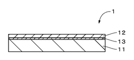
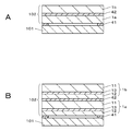
- FIG. 1 is a cross-sectional view illustrating a configuration example of a transparent conductor according to the first embodiment of the present technology.
- FIG. 2 is a cross-sectional view illustrating a configuration example of the transparent conductor according to the second embodiment of the present technology.
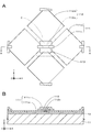
- FIG. 3A is a plan view illustrating a configuration example of a transparent conductor according to a third embodiment of the present technology.
- FIG. 3B is a cross-sectional view illustrating a configuration example of the transparent conductor according to the third embodiment of the present technology.
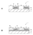
- FIG. 4A is an enlarged cross-sectional view of a part of the transparent conductor shown in FIG. 3B.
- FIG. 4B is a cross-sectional view showing a modification of the transparent conductor according to the third embodiment of the present technology.
- FIG. 1 is a cross-sectional view illustrating a configuration example of a transparent conductor according to the first embodiment of the present technology.
- FIG. 2 is a cross-sectional view illustrating a configuration example
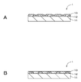
- FIG. 5A and FIG. 5B are cross-sectional views illustrating modifications of the transparent conductor according to the third embodiment of the present technology.
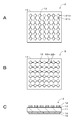
- FIG. 6A is a plan view showing one surface side of a transparent conductor according to a fourth embodiment of the present technology.
- FIG. 6B is a plan view showing the other surface side of the transparent conductor according to the fourth embodiment of the present technology.
- FIG. 6C is a cross-sectional view illustrating a configuration example of the transparent conductor according to the fourth embodiment of the present technology.
- 7A and 7B are cross-sectional views showing a modification of the transparent conductor according to the fourth embodiment of the present technology.
- FIG. 8A is a plan view illustrating a configuration example of an information input device according to the fifth embodiment of the present technology.
- FIG. 8B is a cross-sectional view illustrating a configuration example of the first transparent conductor and the second transparent conductor.
- FIG. 9 is a cross-sectional view illustrating a configuration example of the information input device according to the sixth embodiment of the present technology.
- FIG. 10A is a plan view illustrating a specific example of the information input device according to the seventh embodiment of the present technology.
- FIG. 10B is a cross-sectional view along the line aa shown in FIG. 10A.
- FIG. 11A is an enlarged plan view showing the vicinity of the intersection C shown in FIG. 10A.
- FIG. 11B is a sectional view taken along line AA shown in FIG. 11A.
- FIG. 12 is a cross-sectional view illustrating a configuration example of the information input device according to the eighth embodiment of the present technology.
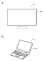
- FIG. 13A is an external view illustrating an example of a television device as an electronic apparatus.
- FIG. 13B is an external view illustrating an example of a notebook personal computer as an electronic apparatus.
- FIG. 14A is an external view illustrating an example of a mobile phone as an electronic apparatus.
- FIG. 14B is an external view illustrating an example of a tablet computer as an electronic device.
- the technique of dye-treating the surface of the metal filler can reduce the reflection L value, but has the problem of increasing the sheet resistance. Therefore, as a result of intensive studies to improve this point, the present inventors have previously protected sites after the surface treatment of the dye with thiols and / or sulfides in order to easily elute the metal on the surface of the metal filler. As a result, the inventors have found a technique capable of reducing the increase in sheet resistance of the surface of the dye without the above protection. However, even with this technique, it is difficult to completely suppress an increase in sheet resistance. Therefore, the present inventors have intensively studied a technique that can further suppress an increase in sheet resistance. As a result, it came to find the structure provided with the transparent conductive layer containing a metal filler, and the light transmissive layer containing a light absorption material.
- FIG. 1 is a cross-sectional view illustrating a configuration example of a transparent conductor according to the first embodiment of the present technology.
- the transparent conductor 1 includes a base material 11, a black float prevention layer 13 that is a light transmission layer, and a transparent conductive layer 12.
- the black float prevention layer 13 and the transparent conductive layer 12 are laminated on the surface of the substrate 11.
- the black float prevention layer 13 is provided between the base material 11 and the transparent conductive layer 12.
- the transparent conductor 1 is suitable for application to a display device or an information input device. In particular, it is suitable for application to a capacitive touch panel.
- the base material 11 is, for example, a transparent inorganic base material or plastic base material.
- a shape of the substrate 11 for example, a film shape, a sheet shape, a plate shape, a block shape, or the like can be used.
- the material of the inorganic base material include quartz, sapphire, and glass.
- a material for the plastic substrate for example, a known polymer material can be used. Specific examples of known polymer materials include triacetyl cellulose (TAC), polyester (TPEE), polyethylene terephthalate (PET), polyethylene naphthalate (PEN), polyimide (PI), polyamide (PA), and aramid.
- the base material 11 is not limited to the above example, and a base material containing an inorganic filler and a polymer material can also be used.
- a pattern or pattern may be printed or vapor-deposited on the substrate 11.
- the thickness of the substrate 11 is preferably in the range of 5 ⁇ m to 5 mm, but is not particularly limited to this range, and can be freely selected in consideration of light transmittance, water vapor transmittance, and the like. Can do.
- the transparent conductive layer 12 contains a metal filler.
- the transparent conductive layer 12 preferably further contains a binder from the viewpoint of improving adhesion with the black float prevention layer 13.
- the metal filler is preferably dispersed in the binder.
- the transparent conductive layer 12 may further contain additives such as a dispersant, a thickener, and a surfactant as components other than the above as necessary.
- the transparent conductive layer 12 may contain a carbon filler as necessary.
- An overcoat layer may be laminated on the transparent conductive layer 12 for the purpose of protecting the transparent conductive layer 12. It is preferable that the overcoat layer has optical transparency with respect to visible light.
- the overcoat layer is made of, for example, a polyacrylic resin, a polyamide resin, a polyester resin, or a cellulose resin, or a hydrolysis or dehydration condensate of a metal alkoxide.
- the overcoat layer may contain a light absorbing material. Moreover, it is preferable that such an overcoat layer is comprised by the film thickness which does not inhibit the light transmittance with respect to visible light. At least a part of the metal filler may be exposed from the surface of the overcoat layer.
- the overcoat layer may have at least one function selected from a functional group consisting of a hard coat function, an antiglare function, an antireflection function, an anti-Newton ring function, an antiblocking function, and the like.
- the metal filler contains a metal material as a main component.
- a metal material for example, at least one selected from the group consisting of Ag, Au, Ni, Cu, Pd, Pt, Rh, Ir, Ru, Os, Fe, Co, and Sn can be used.
- the shape of the metal filler examples include a spherical shape, an ellipsoidal shape, a needle shape, a plate shape, a scale shape, a tube shape, a fiber shape, a rod shape (rod shape), and an indefinite shape. It is not a thing.
- the fiber shape includes a wire shape.
- the wire-like metal filler is referred to as “metal wire”. Two or more kinds of metal fillers having the above shapes may be used in combination.
- the spherical shape includes not only a true spherical shape but also a substantially spherical shape in which the true spherical shape is slightly flattened or distorted.
- the ellipsoidal shape includes not only a strict ellipsoidal shape but also an almost ellipsoidal shape in which the strict ellipsoidal shape is slightly flattened or distorted.
- the metal filler is, for example, a fine metal nanofiller having a diameter on the order of nm.
- the metal filler is a metal wire
- the preferred shape is that the average minor axis diameter is greater than 1 nm and not greater than 500 nm, and the average major axis length is greater than 1 ⁇ m and not greater than 1000 ⁇ m.
- the average minor axis diameter is 1 nm or less, the conductivity of the metal wire is deteriorated and it is difficult to function as a conductive layer after coating.
- the average minor axis diameter is larger than 500 nm, the total light transmittance of the transparent conductive layer 12 is deteriorated.
- the metal wires are not easily connected to each other, and the transparent conductive layer 12 is difficult to function as a conductive layer.
- the average major axis length is longer than 1000 ⁇ m, the total light transmittance of the transparent conductive layer 12 is deteriorated and the dispersibility of the metal wire in the coating used for forming the transparent conductive layer 12 tends to be deteriorated. is there.
- the metal nanoparticles may be connected in a bead shape to have a wire shape. In this case, the length is not limited.
- the basis weight of the metal wire is preferably 0.001 to 1.000 [g / m 2 ].
- the basis weight is less than 0.001 [g / m 2 ]
- the metal wire is not sufficiently present in the transparent conductive layer 12, and the conductivity of the transparent conductive layer 12 is deteriorated.
- the sheet resistance value decreases.
- the basis weight exceeds 1.000 [g / m 2 ]
- the total light transmittance of the transparent conductive layer 12 deteriorates.
- Binder The binder is not particularly limited as long as sufficient adhesion can be obtained after curing, and both an organic binder and an inorganic binder can be used. Binders include polymerization initiators, light stabilizers, UV absorbers, light absorbing materials, antistatic agents, lubricants, leveling agents, antifoaming agents, flame retardants, infrared absorbers, surfactants, viscosity modifiers as additives. A stabilizer such as a dispersant, a curing accelerating catalyst, a plasticizer, an antioxidant or an antisulfurizing agent may be included as necessary.
- thermoplastic resin for example, resin materials such as known transparent natural polymer resins and synthetic polymer resins can be used. More specifically, as the organic binder, a thermoplastic resin, a thermosetting resin, and an energy ray curable resin can be used alone or in admixture of two or more.
- thermoplastic resin include polyvinyl chloride, vinyl chloride-vinyl acetate copolymer, polymethyl methacrylate, nitrocellulose, chlorinated polyethylene, chlorinated polypropylene, vinylidene fluoride, ethyl cellulose, and hydroxypropyl methyl cellulose.
- the energy ray curable resin means a resin that can be cured by irradiation with energy rays.
- Energy rays are polymerization reactions of radicals such as electron beams, ultraviolet rays, infrared rays, laser beams, visible rays, ionizing radiation (X rays, ⁇ rays, ⁇ rays, ⁇ rays, etc.), microwaves, high frequencies, cations, anions, etc. Shows energy lines that can trigger.
- the energy ray curable resin may be used by mixing with another resin as necessary, and may be used by mixing with another curable resin such as a thermosetting resin.
- the energy ray curable resin may be an organic-inorganic hybrid material. Further, two or more kinds of energy ray curable resins may be mixed and used. As the energy ray curable resin, it is preferable to use an ultraviolet curable resin that is cured by ultraviolet rays.
- Thermosetting resins and energy ray curable resin compositions include silicone resins such as melamine acrylate, urethane acrylate, isocyanate, epoxy resin, polyimide resin, acrylic modified silicate, polyvinyl alcohol resin, polyvinyl pyrrolidone resin, and saponified polyvinyl acetate.
- silicone resins such as melamine acrylate, urethane acrylate, isocyanate, epoxy resin, polyimide resin, acrylic modified silicate, polyvinyl alcohol resin, polyvinyl pyrrolidone resin, and saponified polyvinyl acetate.
- examples include resins, polyoxyalkylene resins, polyacrylamide resins, and cellulose resins.
- the inorganic binder is not particularly limited as long as adhesiveness and transparency can be sufficiently obtained.
- examples thereof include hydrolyzed / dehydrated condensates of metal alkoxides.
- Specific examples of such materials include SiO 2 , TiO 2 , ZnO, and the like.
- the black float prevention layer 13 is a light transmission layer (filter layer) that transmits visible light incident on the transparent conductor 1.
- the transmittance of the black float prevention layer 13 with respect to visible light is preferably 50% or more, more preferably 70% or more, and still more preferably 90% or more. If the transmittance is less than 50%, it becomes difficult to apply the transparent conductor 1 to a display device, an information input device, or the like.
- the visible light means light having a wavelength band of about 360 nm or more and 830 nm or less.
- the black float prevention layer 13 is an optical layer including a light absorbing material that absorbs at least visible light, a so-called filter layer. From the viewpoint of improving adhesion to the base material 11, the black float prevention layer 13 preferably further includes a binder. The light absorbing material is preferably dispersed in the binder.
- the transparent conductive layer 12 may further contain additives such as a curing agent, a catalyst agent, a dispersant, a surfactant, and a viscosity modifier as components other than the above, as necessary.
- the light-absorbing material is not particularly limited as long as it has the property of absorbing at least visible light and can improve the contrast of the transparent conductor 1, and is either an organic material or an inorganic material. Can be used regardless of whether it is a conductive material or a non-conductive material.
- As the light-absorbing material a material that does not cause deterioration in characteristics such as an increase in sheet resistance, a decrease in transmittance, and an increase in haze of the transparent conductor 1, or a material that can suppress such deterioration in characteristics is preferable. Considering such a viewpoint, it is preferable to use at least one of a colored compound and a carbon material that absorb at least visible light as the light absorbing material. From the viewpoint of improving the transmission characteristics of the transparent conductor 1, a light absorbing material that can obtain a high aperture ratio is preferable.
- the binder is the same as the binder included in the transparent conductive layer 12 described above.
- the colored compound has, for example, a chromophore [R] having absorption in the visible light region.
- the chromophore [R] is, for example, at least one selected from the group consisting of an unsaturated alkyl group, an aromatic ring, a heterocyclic ring, and a metal ion.
- Specific examples of such chromophore [R] include nitroso group, nitro group, azo group, methine group, amino group, ketone group, thiazolyl group, naphthoquinone group, stilbene derivative, indophenol derivative, diphenylmethane derivative, anthraquinone derivative.
- Triarylmethane derivatives diazine derivatives, indigoid derivatives, xanthene derivatives, oxazine derivatives, phthalocyanine derivatives, acridine derivatives, thiazine derivatives, sulfur atom-containing compounds, metal ion-containing compounds, and the like.
- the chromophore [R] at least one selected from the group consisting of the chromophores exemplified above and compounds containing the same can be used.
- the chromophore [R] At least one selected from the group consisting of cyanine, quinone, ferrocene, triphenylmethane and quinoline as the chromophore [R]. Further, as the chromophore [R], at least one selected from the group consisting of a Cr complex, a Cu complex, an azo group, an indoline group, and a compound containing the same may be used.
- Examples of the colored compound as described above include dyes such as acid dyes and direct dyes.
- dyes such as acid dyes and direct dyes.
- a more specific dye as a dye having a sulfo group, Nippon Kayaku Co., Ltd. Kayakalan BordeauxBL, Kayakalan Brown GL, Kayakalan Gray BL167, Kayakalan Yellow GL143, Kayakalan Black 2RL, Kayakalan Black BGL, Kayakalan Orange RL, Kayarus Cupro Green G, Kayaru Supra Blue MRG, Kayaru Supra Scarlet BNL200, Lanyl Olive manufactured by Taoka Chemical Co., Ltd.
- Examples include BG.
- Nippon Kayaku Co., Ltd.Kayalon Polyester Blue 2R-SF, Kayalon Microester Red AQ-LE, Kayalon Polyester Black ECX300, Kayalon Examples include Microester Blue AQ-LE.
- the dye having a carboxyl group include dyes for dye-sensitized solar cells.
- Ru complexes N3, N621, N712, N719, N749, N773, N790, N820, N823, N845, N886, N945, K9, K19 , K23, K27, K29, K51, K60, K66, K69, K73, K77, Z235, Z316, Z907, Z907Na, Z910, Z991, CYC-B1, HRS-1,
- Anthocyanine WMC234, WMC236, WMC239 , WMC273, PPDCA, PTCA, BBAPDC, NKX-2311, NKX-2510, NKX-2553 (made by Hayashibara), NKX-2554 (made by Hayashibara), NKX-2569, NKX-2586, NKX-2587 (Made by Hayashibara), NKX-2677 (Made by Hayashibara), NKX-2697, NKX-2753, NKX-2883,
- a colored compound used as a paint can also be used, for example, Opera Red, Permanent Scarlet, Carmine, Violet, Lemon Yellow, Permanent Yellow Deep, Sky Blue, Permanent Green manufactured by Turner Color Co., Ltd. List light, permanent green middle, burnt chenner, yellow ocher, permanent orange, permanent lemon, permanent red, viridian (Hugh), cobalt blue (Hugh), Prussian blue (Hugh), jet black, permanent scarlet and violet Can do. Also, for example, Bright Red, Cobalt Blue Hue, Ivory Black, Yellow Ocher, Permanent Green Light, Permanent Yellow Light, Burnt Senna, Ultramarine Deep, Vermillion Hugh and Permanent Green, which are colored compounds manufactured by Holbein Industry Co., Ltd. Etc. can also be used. Among these colored compounds, permanent scarlet, violet and jet black (manufactured by Turner Color Co., Ltd.) are preferable.
- edible colored compounds can also be used as the colored compounds.
- edible red No. 2 amaranth edible red No. 3 erythrosin, edible red No. 102 New Coxin, edible red No. 104 Phloxine manufactured by Daiwa Kasei Co., Ltd.
- Food Red 105 Rose Bengal Food Red 106 Acid Red, Food Blue 1 Brilliant Blue, Food Red 40 Allura Red, Food Blue 2 Indigo Carmine, Red 226 Helidon Pink CN, Red 227 First Acid Magenta Red No. 230 eosin YS, green No. 204 pyranin conc, orange No. 205 orange II, blue No. 205 alphazurin, purple No. 401 arizurol purple and black No. 401 naphthol blue black.
- Natural colored compounds can also be used, such as High Red G-150 (water-soluble and grape skin pigment), Cochineal Red AL (water-soluble and cochineal pigment), High Red MC (produced by Daiwa Kasei Co., Ltd.) Water-soluble / cochineal dye), High Red BL (water-soluble / beet red), Daiwamonas LA-R (water-soluble / Benicouji dye), High Red V80 (water-soluble, purple potato dye), Annatto N2R-25 (water dispersibility) Anato dye), Annatto WA-20 (water-soluble anato-anato dye), high orange SS-44R (water dispersible, low-viscosity product, red pepper dye), high orange LH (oil-soluble red pepper dye), high green B (Water-soluble, green colorant formulation), High green F (Water-soluble, green colorant formulation), High blue AT (Water-soluble, colorant formulation) Pear blue pigment), Himelon P-2 (water-soluble, green colorant formulation),
- Carbon material examples include carbon, carbon black, acetylene black, graphene, carbon nanotube, carbon microcoil, carbon nanohorn, pyrolytic graphite (HOPG), natural graphite, vapor grown carbon fiber (VGCF), and pitch-based carbon fiber. And at least one selected from the group consisting of mesocarbon microbeads (MCMB) and the like can be used.
- MCMB mesocarbon microbeads
- the shape of the carbon material examples include a spherical shape, an ellipsoidal shape, a needle shape, a plate shape, a scale shape, a tube shape, a wire shape, a rod shape (rod shape), a fiber shape, and an indefinite shape. It is not limited. Two or more carbon materials having the above shapes may be used in combination.
- the spherical shape includes not only a true spherical shape but also a shape in which the true spherical shape is slightly flattened or distorted, a shape in which irregularities are formed on the true spherical surface, or a shape in which these shapes are combined.
- the ellipsoidal shape is not only a strict ellipsoidal shape, but a strict ellipsoidal shape that is slightly flattened or distorted, a shape in which irregularities are formed on a strict ellipsoidal surface, or a combination of these shapes.
- the shape is also included.
- a paint for forming a black anti-floating layer is prepared by dispersing a light absorbing material in a solvent. If necessary, a binder and / or an additive may be further added to the solvent. For the purpose of improving the coating property to the substrate 11 and the pot life of the composition, additives such as a surfactant, a viscosity modifier and a dispersant may be added as necessary.
- a dispersion method it is preferable to use stirring, ultrasonic dispersion, bead dispersion, kneading, homogenizer treatment, or the like.
- the solvent is not particularly limited as long as it can dissolve and disperse the light absorbing material.
- a coating material for forming a transparent conductive layer is prepared by adding a metal filler to a solvent and dispersing it. If necessary, a binder and / or additive may be further added. For example, a dispersant for improving the dispersibility of the metal filler and other additives for improving adhesion and durability may be added.
- a dispersion method it is preferable to use stirring, ultrasonic dispersion, bead dispersion, kneading, homogenizer treatment, or the like.
- the amount of the metal filler in the paint is 0.01 to 10.00 parts by mass.
- a sufficient basis weight for example, 0.001 to 1.000 [g / m 2 ]
- the dispersibility of the metal filler tends to deteriorate.
- it is preferable to make it the addition amount of the grade which the electroconductivity of the transparent conductive layer 12 finally obtained does not deteriorate.
- the solvent is not particularly limited as long as it can disperse the metal filler.
- water eg, water, alcohol (eg, methanol, ethanol, n-propanol, i-propanol, n-butanol, i-butanol, sec-butanol, tert-butanol, etc.), anone (eg, cyclohexanone, cyclopentanone), amide
- At least one selected from for example, N, N-dimethylformamide: DMF), sulfide (for example, dimethylsulfoxide: DMSO) and the like is used.
- a high boiling point solvent may be further added as a solvent to control the evaporation rate of the solvent from the paint.
- the high boiling point solvent include butyl cellosolve, diacetone alcohol, butyl triglycol, propylene glycol monomethyl ether, propylene glycol monoethyl ether, ethylene glycol monoethyl ether, ethylene glycol monopropyl ether, ethylene glycol monoisopropyl ether, diethylene glycol monobutyl ether.
- Diethylene glycol monoethyl ether Diethylene glycol monoethyl ether, diethylene glycol monomethyl ether diethylene glycol diethyl ether, dipropylene glycol monomethyl ether, tripropylene glycol monomethyl ether, propylene glycol monobutyl ether, propylene glycol isopropyl ether, dipropylene glycol isopropyl ether, triplicate Propylene glycol isopropyl ether, methyl glycol.
- These high boiling solvents may be used alone or in combination.
- a coating film is formed on the surface of the base material 11 using the paint for forming a black float prevention layer prepared as described above.
- the method for forming the coating film is not particularly limited, but in consideration of physical properties, convenience, production cost and the like, a wet film forming method is preferable.
- a wet film forming method for example, a known method such as a coating method, a spray method, or a printing method can be used.
- the coating method is not particularly limited, and a known coating method can be used.
- Known coating methods include, for example, micro gravure coating method, wire bar coating method, direct gravure coating method, die coating method, dip method, spray coating method, reverse roll coating method, curtain coating method, comma coating method, knife coating method. And spin coating method.
- the printing method include a relief printing method, an offset printing method, a gravure printing method, an intaglio printing method, a rubber plate printing method, a screen printing method, and an ink jet printing method.
- the solvent is volatilized by drying the coating film formed on the surface of the substrate 11. Drying conditions are not particularly limited, and may be either natural drying or heat drying. Heat drying may also serve as a firing step. Thereby, the black float prevention layer 13 is formed on the surface of the substrate 11.
- the coating film in which the metal filler is dispersed is formed on the surface of the black float prevention layer 13 using the coating material for forming the transparent conductive layer prepared as described above.
- the method for forming the coating film is not particularly limited, but in consideration of physical properties, convenience, production cost and the like, a wet film forming method is preferable.
- a wet film forming method for example, a known method such as a coating method, a spray method, or a printing method can be used.
- the coating method is not particularly limited, and a known coating method can be used.
- Known coating methods include, for example, micro gravure coating method, wire bar coating method, direct gravure coating method, die coating method, dip method, spray coating method, reverse roll coating method, curtain coating method, comma coating method, knife coating method. And spin coating method.
- the printing method include a relief printing method, an offset printing method, a gravure printing method, an intaglio printing method, a rubber plate printing method, a screen printing method, and an ink jet printing method.
- the solvent in the coating film formed on the surface of the black float prevention layer 13 is dried and removed. Drying conditions are not particularly limited, and may be either natural drying or heat drying.
- the uncured binder is cured by heat treatment or energy beam irradiation, for example. Thereby, it will be in the state by which the metal filler was disperse
- the binder is an energy ray curable resin
- the uncured binder may be cured in a pattern by irradiation with energy rays via a photomask.
- An electrode in which transparent conductive portions and transparent insulating portions are alternately arranged in a plane on the surface of the black float prevention layer 13 by forming an etching mask on the surface of the transparent conductive layer 12 and performing an etching process on the transparent conductive layer 12 A pattern may be formed.
- the black float prevention layer 13 between the base material 11 and the transparent conductive layer 12, the light reflected by the metal filler contained in the transparent conductive layer 12 can be used as a black float prevention layer. It can be absorbed by 13 light absorbing materials. Therefore, the contrast of the transparent conductor 1 can be improved.
- the contrast of the transparent conductor 1 is improved by further providing the black float prevention layer 13 instead of adding a surface treatment to the metal filler, the sheet resistance is increased while realizing a high contrast. There is nothing. In a range where a desired sheet resistance value can be obtained, at least a part of the surface of the metal filler may be covered with the elemental compound by surface-treating the metal filler with the colored compound. This further improves the contrast.
- the same compound as the colored compound contained in the black float prevention layer 13 can be used.
- the colored compound may be adsorbed on the surface of the metal filler, for example.
- the adsorption means a phenomenon that remains on the surface of the metal filler or in the vicinity thereof.
- the adsorption may be chemical adsorption or physical adsorption, or a combination thereof.
- Chemisorption means adsorption that occurs with chemical bonds such as covalent bonds, ionic bonds, metal bonds, coordinate bonds, and hydrogen bonds between the surface of the metal filler and the colored compound.
- Physical adsorption means adsorption caused by interaction such as van der Waals force, electrostatic attraction, magnetic force and the like.
- the transparent conductor 1 having the following configuration (1) has been described.
- the configuration of the transparent conductor 1 is not limited to this.
- the following configurations (2) to (15) can be adopted as the configuration of the transparent conductor 1.
- Transparent conductive layer / black floating prevention layer / base material (2) Transparent conductive layer / black floating prevention layer / anchor layer / base material (3) Black floating prevention layer / transparent conductive layer / base material (4) Black floating Prevention layer / Transparent conductive layer / Anchor layer / Base material (5) Black float prevention layer / Transparent conductive layer / Black float prevention layer / Base material (6) Black float prevention layer / Transparent conductive layer / Black float prevention layer / Anchor layer / Substrate (7) Transparent conductor in any one of configurations (1) to (6) / Hard coat layer (8) Transparent conductor in any one of (1) to (7) / Antireflection layer (9) ( 1)-(7) transparent conductor / moth eye structure layer (10) (1)-(9) transparent conductor / adhesive layer / substrate (11) substrate / adhesive layer / configuration (1) to (10) transparent conductor (12) overcoat layer / configuration (1) to (11) transparent conductor (13) antireflection layer / structure (1) to (12) transparent conductor (14) moth
- the anchor layer has optical transparency with respect to visible light.
- the anchor layer is made of, for example, a polyacrylic resin, a polyamide resin, a polyester resin, or a cellulose resin, or is made of a hydrolysis or dehydration condensate of a metal alkoxide.
- the anchor layer is preferably formed with a film thickness that does not impair the light transmittance with respect to visible light.
- FIG. 2 is a cross-sectional view illustrating a configuration example of the transparent conductor according to the second embodiment of the present technology.
- the transparent conductor 2 according to the second embodiment is different from the transparent conductor 1 according to the first embodiment in that it further includes a transparent conductive layer 14 and a black float prevention layer 15.
- the transparent conductive layer 14 is provided on the surface of the base 11 opposite to the side on which the transparent conductive layer 12 is provided.
- the black float prevention layer 15 is provided on the surface of the transparent conductive layer 14.
- the configuration and formation method of the transparent conductive layer 14 are the same as those of the transparent conductive layer 12 in the first embodiment.
- the configuration and formation method of the black float prevention layer 15 are the same as those of the transparent conductive layer 12 in the first embodiment.
- FIG. 3A is a plan view illustrating a configuration example of a transparent conductor according to a third embodiment of the present technology.
- FIG. 3B is a cross-sectional view illustrating a configuration example of the transparent conductor according to the third embodiment of the present technology.
- the transparent conductor 1 according to the third embodiment is the same as the first embodiment in that the transparent conductive layer 12 and the black float prevention layer 13 are patterned in the same shape. It differs from the transparent conductor 1 which concerns.
- the patterned transparent conductive layer 12 constitutes an electrode such as an X electrode or a Y electrode, for example. As this electrode, as shown to FIG.
- FIG. 3A what is provided with several pad part (unit electrode body) 21m and several connection part 21n which connects several pad parts 21m can be used.
- the configuration of the electrode is not limited to this example, and for example, a striped (straight) electrode can be used.
- FIG. 3B shows an example in which the transparent conductive layer 12 and the black float prevention layer 13 are patterned in the same shape, but the black float prevention layer 13 is not patterned, and the substrate 11 The entire electrode formation region may be continuously covered.
- FIG. 4A is an enlarged cross-sectional view showing a part of the patterned transparent conductive layer 12 and black float prevention layer 13.
- FIG. 4A an example of the transparent conductive layer 12 including the metal wire 31 and the binder 32 is shown.
- the insulating region 22 between the electrodes 21 is configured by removing the transparent conductive layer 12 between the electrodes 21.
- the configuration of the insulating region 22 is not limited to this example, and the insulating region 22 between the electrodes 21 is configured by dividing the metal wire 31 as shown in FIG. 4B. Also good.
- the film also remains in the portion of the transparent conductive layer 12 that becomes the insulating region 22.
- the state in which the metal wire 31 described above is divided can be obtained by adjusting the etching conditions of the transparent conductive layer 12 in the manufacturing process of the transparent conductor 1.
- the black float prevention layer 13 is provided on the surface of the patterned transparent conductive layer 12, the black float prevention layer 13 is provided so as to follow the shape of the patterned transparent conductive layer 12 as shown in FIG. 5A. It may be. Further, as shown in FIG. 5B, the patterned transparent conductive layer 12 may be embedded in the black float prevention layer 13 so that the surface of the black float prevention layer 13 becomes flat.
- FIG. 6A is a plan view showing one surface side of a transparent conductor according to a fourth embodiment of the present technology.
- FIG. 6B is a plan view showing the other surface side of the transparent conductor according to the fourth embodiment of the present technology.
- FIG. 6C is a cross-sectional view illustrating a configuration example of the transparent conductor according to the fourth embodiment of the present technology.
- the transparent conductive layer 12 and the black anti-floating layer 13 on one surface (first surface) side are patterned in the same shape.
- the transparent conductive layer 14 on the other surface (second surface) side and the black float prevention layer 15 are patterned in the same shape, which is different from the transparent conductor 2 according to the second embodiment. ing. When viewed from the direction perpendicular to the surface of the transparent conductor 2, the patterned transparent conductive layer 12 and the transparent conductive layer 14 are in a crossing relationship.
- the patterned transparent conductive layer 12 constitutes an X electrode, for example.
- This electrode as shown to FIG. 6A, what is provided with several pad part (unit electrode body) 21m and several connection part 21n which connects several pad parts 21m can be used.
- the configuration of the electrode is not limited to this example, and for example, a striped (straight) electrode can be used.
- the patterned transparent conductive layer 14 constitutes, for example, a Y electrode.
- this electrode as shown to FIG. 6B, what is provided with the some pad part (unit electrode body) 22m and the some connection part 22n which connects the some pad part 22m can be used.
- the configuration of the electrode is not limited to this example, and for example, a striped (straight) electrode can be used.
- the transparent conductive layer 12 and the black float prevention layer 13 are patterned in the same shape, and the transparent conductive layer 14 and the black float prevention layer 15 are patterned in the same shape.
- the black float prevention layers 13 and 15 may be unpatterned and may continuously cover the entire electrode formation region of the substrate 11.
- the black float prevention layer 13 is provided on the surface of the patterned transparent conductive layer 12, the black float prevention layer 13 is provided so as to follow the shape of the patterned transparent conductive layer 12, as shown in FIG. 7A. It may be. Further, as shown in FIG. 7B, the patterned transparent conductive layer 12 may be embedded in the black float prevention layer 13 so that the surface of the black float prevention layer 13 becomes flat.
- FIG. 8A is a cross-sectional view illustrating a configuration example of an information input device according to a fifth embodiment of the present technology.
- the information input device 102 is provided on the display surface of the display device 101.
- the information input device 102 is bonded to the display surface of the display device 101 by a bonding layer 41, for example.
- the bonding layer 41 may be provided only at the peripheral edge between the display surface of the display device 101 and the back surface of the information input device 102.
- As the bonding layer 41 for example, an adhesive paste, an adhesive tape, or the like is used.
- the surface on the touch surface (information input surface) side for inputting information with a finger or a pen is referred to as “front surface”, and the surface on the opposite side is referred to as “back surface”.
- the display device 101 to which the information input device 102 is applied is not particularly limited.
- a liquid crystal display a CRT (Cathode Ray Tube) display, a plasma display panel (PDP), electroluminescence (
- Various display devices such as an electro luminescence (EL) display and a surface-conduction electron-emitter display (SED) can be used.
- EL electro luminescence
- SED surface-conduction electron-emitter display
- the information input device 102 is a so-called projected capacitive touch panel, and includes a first transparent conductor 1a and a second transparent conductor 1b provided on the surface of the first transparent conductor 1a.
- the 1 transparent conductor 1a and the 2nd transparent conductor 1b are bonded together through the bonding layer 42.
- FIG. 1 is a so-called projected capacitive touch panel, and includes a first transparent conductor 1a and a second transparent conductor 1b provided on the surface of the first transparent conductor 1a.
- the 1 transparent conductor 1a and the 2nd transparent conductor 1b are bonded together through the bonding layer 42.
- FIG. 8B is a cross-sectional view illustrating a configuration example of the first transparent conductor and the second transparent conductor.
- the transparent conductor 1 As the first transparent conductor 1a and the second transparent conductor 1b, the transparent conductor 1 according to the third embodiment described above can be used.
- the electrode of the first transparent conductor 1a (the patterned transparent conductive layer 12) and the electrode of the second transparent conductor 1b (the patterned transparent conductive layer 12) are from a direction perpendicular to the surface of the information input device 102. When viewed, they are in a crossing relationship.
- the black float prevention layer 13 that is a light transmission layer is preferably provided at a position closer to the touch surface than the transparent conductive layer 12. This is because light reflected on the touch surface side (user side) by the metal filler contained in the transparent conductive layer 12 can be absorbed by the light absorption material of the black float prevention layer 13.
- the black float prevention layer 13 which is a light transmission layer is provided at a position closer to the touch surface than the transparent conductive layer 12. This is because light reflected on the touch surface side (user side) by the metal filler contained in the transparent conductive layer 12 can be absorbed by the light absorption material of the black float prevention layer 13.
- FIG. 9 is a cross-sectional view illustrating a configuration example of the information input device according to the sixth embodiment of the present technology. As shown in FIG. 9, the information input device 102 is different from the fifth embodiment in that it includes a transparent conductor 2 according to the fourth embodiment.
- the transparent conductive layer 14 and the black float prevention layer 15 are stacked on the touch surface side of the transparent conductor 2, and the transparent conductive layer 12 and the black float prevention layer 13 are laminated on the back side opposite to the transparent conductive layer 14.
- the black floating prevention layer 15 is preferably provided at a position closer to the touch surface than the transparent conductive layer 14.
- the black float prevention layer 13 is preferably provided at a position closer to the touch surface than the transparent conductive layer 12.
- the protective layer 44 is, for example, a top plate made of glass or plastic.
- the protective layer 44 and the transparent conductor 2 are bonded together via the bonding layer 43, for example.
- the protective layer 44 is not limited to this example, and may be a ceramic coat (overcoat) such as SiO 2 .
- FIG. 10A is a plan view illustrating a configuration example of an information input device according to a seventh embodiment of the present technology.
- FIG. 10B is a cross-sectional view along the line aa shown in FIG. 10A.
- the information input device 102 is a so-called projected capacitive touch panel, and as shown in FIGS. 10A and 10B, the base material 11, the black float prevention layer 13, a plurality of transparent electrode portions 111 and transparent electrode portions 112. And a transparent insulating layer 113.
- the plurality of transparent electrode portions 111 and the transparent electrode portion 112 are provided on the same surface of the substrate 11.
- the black float prevention layer 13 is provided between the base material 11 and the plurality of transparent electrode portions 111 and the transparent electrode portion 112.
- the black float prevention layer 15 which is a light transmission layer is preferably provided at a position closer to the touch surface than the plurality of transparent electrode portions 111 and the transparent electrode portions 112.
- the transparent insulating layer 113 is interposed between the intersecting portions of the transparent electrode portion 111 and the transparent electrode portion 112.
- an optical layer 121 may be further provided on the surface of the base material 11 on which the transparent electrode part 111 and the transparent electrode part 112 are formed, as necessary.
- the optical layer 121 is not shown.
- the optical layer 121 includes a bonding layer 122 and a base 123, and the base 123 is bonded to the surface of the base material 11 via the bonding layer 122.
- the information input device 102 is suitable for application to a display surface of a display device.
- the base material 11 and the optical layer 121 have transparency with respect to visible light, for example, and the refractive index n is preferably in the range of 1.2 or more and 1.7 or less.
- X-axis direction two directions orthogonal to each other within the surface of the information input device 102 are referred to as an X-axis direction and a Y-axis direction, respectively, and a direction perpendicular to the surface is referred to as a Z-axis direction.
- the transparent electrode portion 111 extends in the X-axis direction (first direction) on the surface of the base material 11, while the transparent electrode portion 112 extends in the Y-axis direction (second direction on the surface of the base material 11. Direction). Therefore, the transparent electrode portion 111 and the transparent electrode portion 112 intersect each other at right angles. At the intersection C where the transparent electrode portion 111 and the transparent electrode portion 112 intersect, a transparent insulating layer 113 for insulating the two electrodes is interposed.
- FIG. 11A is an enlarged plan view showing the vicinity of the intersection C shown in FIG. 10A.
- FIG. 11B is a sectional view taken along line AA shown in FIG. 11A.
- the transparent electrode portion 111 includes a plurality of pad portions (unit electrode bodies) 111m and a plurality of connecting portions 111n that connect the plurality of pad portions 111m.
- the connecting portion 111n extends in the X-axis direction and connects the ends of the adjacent pad portions 111m.
- the transparent electrode portion 112 includes a plurality of pad portions (unit electrode bodies) 112m and a plurality of connecting portions 112n that connect the plurality of pad portions 112m.
- the connecting portion 112n extends in the Y-axis direction and connects the ends of the adjacent pad portions 112m.
- connection part 112n In the intersection part C, the connection part 112n, the transparent insulating layer 113, and the connection part 111n are laminated
- the connecting portion 111n is formed so as to cross over the transparent insulating layer 113, and one end of the connecting portion 111n straddling the transparent insulating layer 113 is electrically connected to one of the adjacent pad portions 111m, and the transparent insulating layer The other end of the connecting portion 111n straddling 113 is electrically connected to the other of the adjacent pad portions 111m.
- the pad portion 112m and the connecting portion 112n are integrally formed, whereas the pad portion 111m and the connecting portion 111n are separately formed.
- the pad portion 111m, the pad portion 112m, and the connecting portion 112n are configured by, for example, a single transparent conductive layer provided on the surface of the base material 11. This transparent conductive layer is made of the same material as that of the transparent conductive layer 12 in the first embodiment described above.
- the connecting portion 111n is made of, for example, a conductive layer.
- the shapes of the pad portion 111m and the pad portion 112m for example, a diamond shape (diamond shape), a polygonal shape such as a rectangle, a star shape, a cross shape, or the like can be used. However, the shape is not limited to these shapes. .
- the conductive layer constituting the connecting portion 111n for example, a metal layer or a transparent conductive layer can be used.
- the metal layer contains a metal as a main component.
- a metal having high conductivity examples include Ag, Al, Cu, Ti, Nb, and impurity-added Si. Ag is preferable in consideration of film formability and printability.
- the width of the connecting portion 111n is narrowed, the thickness thereof is thinned, and the length thereof is shortened. Thereby, visibility can be improved.
- the connecting portion 111n and the connecting portion 112n can have a rectangular shape, but the connecting portion 111n and the connecting portion 112n may have any shape as long as the adjacent pad portions 111m and the pad portions 112m can be connected to each other.
- the shape is not particularly limited to a rectangular shape. Examples of shapes other than the rectangular shape include a linear shape, an oval shape, a triangular shape, and an indefinite shape.
- the transparent insulating layer 113 preferably has a larger area than the portion where the connecting portion 111n and the connecting portion 112n intersect.
- the pad portion 111m located at the intersecting portion C and the tip of the pad portion 112m are covered. It has the size.
- the transparent insulating layer 113 contains a transparent insulating material as a main component.
- a transparent insulating material it is preferable to use a polymer material having transparency, and examples of such a material include vinyl monomers such as polymethyl methacrylate, methyl methacrylate and other alkyl (meth) acrylates, and styrene.
- (Meth) acrylic resins such as copolymers; polycarbonate resins such as polycarbonate and diethylene glycol bisallyl carbonate (CR-39); homopolymers or copolymers of (brominated) bisphenol A type di (meth) acrylates
- Thermosetting (meth) acrylic resins such as polymers and copolymers of urethane-modified monomers of (brominated) bisphenol A mono (meth) acrylate; polyesters, especially polyethylene terephthalate, polyethylene naphthalate and unsaturated polyesters Le, acrylonitrile - styrene copolymers, polyvinyl chloride, polyurethane, epoxy resins, polyarylate, polyether sulfone, polyether ketone, cycloolefin polymer (trade name: ARTON, ZEONOR), and the like cycloolefin copolymer. It is also possible to use an aramid resin in consideration of heat resistance.
- the shape of the transparent insulating layer 113 is not particularly limited as long as it is interposed between the transparent electrode portion 111 and the transparent electrode portion 112 at the intersection C and can prevent electrical contact between both electrodes.
- a polygon such as a quadrangle, an ellipse, and a circle can be given as examples.
- the quadrangle include a rectangle, a square, a rhombus, a trapezoid, a parallelogram, and a rectangle with a corner having a curvature R.
- a wiring 115 is electrically connected to one end of each of the transparent electrode portion 111 and the transparent electrode portion 112, and the wiring 115 and a drive circuit (not shown) are connected via an FPC (Flexible Printed Circuit) 114. .
- FPC Flexible Printed Circuit
- FIG. 12 is a plan view illustrating a configuration example of the information input device according to the eighth embodiment of the present technology.
- a black float prevention layer 13 is provided on the surface of the base body 45.
- the base body 45 is provided on the display surface of the information input device 102 such that the black float prevention layer 13 faces the display surface of the information input device 102.
- the base body 45 and the information input device 102 are bonded together by, for example, a bonding layer 46.
- any of the information input devices 102 according to the fifth to seventh embodiments can be used.
- a configuration in which the black float prevention layers 13 and 15 are omitted may be employed. Even in this case, the black float prevention layer 13 provided on the surface of the base body 45 can absorb the light reflected by the metal filler. Therefore, contrast can be improved.
- An electronic apparatus includes any one of the information input devices 102 according to the fifth to eighth embodiments in a display device.
- the information input device 102 is provided on the surface of the display device or inside the display device.
- An example of an electronic device according to the ninth embodiment of the present technology will be described below.
- FIG. 13A is an external view illustrating an example of a television device as an electronic apparatus.
- the television apparatus 201 includes a display device 202, and includes any of the information input devices 102 according to the fifth to eighth embodiments on the surface or inside of the display device 202.
- FIG. 13B is an external view showing an example of a notebook personal computer as an electronic device.
- the notebook personal computer 211 includes a display device 212, and includes any of the information input devices 102 according to the fifth to eighth embodiments on the surface or inside of the display device 212.
- FIG. 14A is an external view illustrating an example of a mobile phone as an electronic device.
- the mobile phone 221 is a so-called smartphone, and includes a display device 222, and includes any one of the information input devices 102 according to the fifth to eighth embodiments on the surface or inside of the display device 222.
- FIG. 14B is an external view showing an example of a tablet computer as an electronic device.
- the tablet computer 231 includes a display device 232, and any one of the information input devices 102 according to the fifth to eighth embodiments is provided on or inside the display device 232.
- the electronic apparatus according to the ninth embodiment described above includes any of the information input devices 102 according to the fifth to eighth embodiments in the display device, the visibility of the display device can be improved. it can.
- Example 1 Preparation process of paint for forming black float prevention layer
- the following raw materials were mixed and dispersed to prepare a paint for forming a black anti-floating layer.
- the formulation of the paint for forming the black anti-floating layer was prepared, and the content of the black dye in the black anti-floating layer after drying and curing was 0.250% by mass.
- Black dye (Nippon Kayaku Co., Ltd., trade name: Black YA) Transparent resin material (Wako Pure Chemical Industries, Ltd., ethyl cellulose (about 49% ethoxy)) Resin hardener (Asahi Kasei Co., Ltd., trade name: Duranate 17B-60P) Curing accelerator (manufactured by Nitto Kasei Co., Ltd., trade name: Neostan U100)
- silver nanowire was produced as metal nanowire.
- silver nanowires having a diameter of 30 nm and a length of 10 to 30 ⁇ m were prepared by an existing method referring to a document (“ACS Nano” 2010, VOL. 4, NO. 5, p. 2955-2963).
- Silver nanowire transparent resin material ethyl cellulose (about 49% ethoxy) manufactured by Wako Pure Chemical Industries, Ltd.
- Resin hardener Duranate 17B-60P manufactured by Asahi Kasei Corporation
- Curing acceleration catalyst Neostan U100 manufactured by Nitto Kasei Co., Ltd.
- Solvent Isopropyl alcohol (IPA) and methyl ethyl ketone (MEK)
- the paint for forming a black anti-floating layer prepared as described above was applied to the surface of the transparent substrate with a coil bar of a count 8 to form a coating film.
- a sheet having a thickness of 100 ⁇ m (trade name: Diafoil O300E, manufactured by Mitsubishi Resin Co., Ltd.) was used.
- a heat treatment was performed in an oven at 120 ° C. for 5 minutes, and the solvent in the coating film was dried and removed, followed by a heat treatment at 150 ° C. for 30 minutes to cure the transparent resin material in the coating film. .
- a black float prevention layer having a thickness of 10 nm was formed on the surface of the transparent substrate.
- the coating material prepared as described above was applied onto the black float prevention layer with a coil bar of count 8, and a coating film was formed.
- the sheet resistance was set to about 100 ⁇ / ⁇ by setting the basis weight of the silver nanowires to 0.02 g / m 2 or more.
- a heat treatment for 30 minutes was performed in an oven at 120 ° C., and the solvent in the coating film was dried and removed, followed by a heat treatment at 150 ° C. for 30 minutes to cure the transparent resin material in the coating film. .
- the transparent conductive layer was formed on the surface of the black float prevention layer.
- the coating material for forming the protective layer prepared as described above was applied to the surface of the black float prevention layer with an applicator so that the coating thickness (wet thickness) was 116 ⁇ m.
- the coating film was irradiated with UV light with an integrated light amount of 300 mJ / cm 2 .
- an acrylic resin layer having a thickness of about 100 nm was formed on the surface of the transparent conductive layer as a protective layer.
- the intended transparent conductive sheet was obtained.
- Example 2 Transparent in the same manner as in Example 1 except that the formulation of the paint for forming the black float prevention layer was prepared and the content of the black dye in the black float prevention layer after the drying effect was 0.400% by mass. A conductive sheet was obtained.
- Example 3 Transparent in the same manner as in Example 1 except that the formulation of the paint for forming the black float prevention layer was prepared and the content of the black dye in the black float prevention layer after the drying effect was 0.500% by mass. A conductive sheet was obtained.
- Example 4 Carbon nanotubes were used in place of black dye as a raw material for the paint for forming the black anti-floating layer, and the carbon nanotubes in the black anti-floating layer after the drying effect were prepared by preparing a coating composition for forming the black anti-floating layer.
- a transparent conductive sheet was obtained in the same manner as in Example 1 except that the content of A was 0.063% by mass.
- the carbon nanotube a single-walled carbon nanotube (SWCNT: Single Wall Carbon Nano Tube, manufactured by KH Chemicals) was used as the carbon nanotube.
- Example 5 A transparent conductive material was prepared in the same manner as in Example 4 except that the formulation of the paint for forming the black float prevention layer was prepared and the carbon nanotube content in the black float prevention layer after the drying effect was 0.143% by mass. A sheet was obtained.
- Example 6 A transparent conductive material was prepared in the same manner as in Example 4 except that the formulation of the paint for forming the black float prevention layer was prepared and the carbon nanotube content in the black float prevention layer after the drying effect was 0.250% by mass. A sheet was obtained.
- Example 7 A transparent conductive sheet was obtained in the same manner as in Example 1 except that carbon nanotubes were further added as a raw material for the paint for forming the black float prevention layer.
- the mixing ratio (mass ratio) A: B of the black dye A and the carbon nanotube B is 5: 1, and the total content of the black dye A and the carbon nanotube B in the black float prevention layer after the drying effect is
- the formulation of the paint for forming a black float prevention layer was prepared so that it might become 0.286 mass%.
- As the carbon nanotube a single-walled carbon nanotube (SWCNT: Single Wall Carbon Nano Tube, manufactured by KH Chemicals) was used.
- Example 1 A transparent conductive sheet was prepared in the same manner as in Example 1 except that the step of preparing the paint for forming the black float prevention layer and the step of forming the black float prevention layer were omitted and the transparent conductive layer was directly formed on the surface of the substrate. Obtained.
- the reflection L value which is an index of black float, was evaluated from the base material side with a color i5 manufactured by X-Rite Co., Ltd. according to JIS Z8722, with a black tape attached to the transparent conductive layer side.
- Table 1 shows the configurations of the transparent conductive sheets of Examples 1 to 7 and Comparative Example 1.
- Table 2 shows the evaluation results of the transparent conductive sheets of Examples 1 to 7 and Comparative Example 1.
- the present technology can also employ the following configurations.
- the said light absorption material is a transparent conductor as described in (1) which absorbs visible light.
- the said light absorption material is a transparent conductor as described in (1) which is a colored compound which absorbs visible light.
- the said colored compound is a transparent conductor as described in (3) which is dye.
- the colored compound according to (3), wherein the colored compound has a chromophore.
- the transparent conductor according to (1), wherein the light absorbing material is a carbon material.
- the said metal filler is a transparent conductor in any one of (1) to (7) which is a metal wire.
- the light transmitting layer is the transparent conductor according to any one of (1) to (8), which is provided between the base material and the transparent conductive layer.
- the transparent conductive layer according to any one of (1) to (10), wherein the transparent conductive layer further includes a binder.
- a transparent conductive layer containing a metal filler An input device comprising: a light transmission layer including a light absorbing material. (13) The input device according to (12), wherein the light transmission layer is provided at a position closer to the input surface than the transparent conductive layer. (14) A display device and an input device; The input device is A transparent conductive layer containing a metal filler; And a light transmission layer containing a light absorbing material. (15) The display device according to (14), wherein the light transmission layer is provided at a position closer to the input surface than the transparent conductive layer. (16) A substrate; A transparent conductive layer containing a metal filler; A light transmissive layer containing a light absorbing material, and A transparent conductor in which at least a part of the surface of the metal filler is coated with an elemental compound.
Landscapes
- Engineering & Computer Science (AREA)
- General Engineering & Computer Science (AREA)
- Theoretical Computer Science (AREA)
- Human Computer Interaction (AREA)
- Physics & Mathematics (AREA)
- General Physics & Mathematics (AREA)
- Laminated Bodies (AREA)
- Non-Insulated Conductors (AREA)
Description
基材と、
金属フィラーを含む透明導電層と、
光吸収材料を含む光透過層と
を備える透明導電体である。
金属フィラーを含む透明導電層と、
光吸収材料を含む光透過層と
を備える入力装置である。
表示装置と入力装置とを備え、
入力装置は、
金属フィラーを含む透明導電層と、
光吸収材料を含む光透過層と
を備える表示装置である。
基材と、
金属フィラーを含む透明導電層と、
光吸収材料を含む光透過層と
を備え、
金属フィラー表面の少なくとも一部が有素化合物により被覆されている透明導電体である。
上述したように、金属フィラー表面を染料処理する技術では、反射L値を低減することはできるが、シート抵抗の増加を招いてしまうという問題がある。そこで、本発明者らは、この点を改善すべく鋭意検討を重ねた結果、金属フィラー表面において金属が溶出しやすいサイトをチオール類および/またはスルフィド類で予め保護することにより、染料表面処理後のシート抵抗増加を、上記保護無しの染料表面処理時よりも低減できる技術を見出すに至った。しかしながら、この技術でも、シート抵抗の増加を完全に抑制することは困難である。そこで、本発明者らは、シート抵抗の増加をさらに抑制できる技術について鋭意検討を行った。その結果、金属フィラーを含む透明導電層と、光吸収材料を含む光透過層とを備える構成を見出すに至った。
1.第1の実施形態(透明導電体の例)
2.第2の実施形態(透明導電体の例)
3.第3の実施形態(透明導電体の例)
4.第4の実施形態(透明導電体の例)
5.第5の実施形態(情報入力装置の例)
6.第6の実施形態(情報入力装置の例)
7.第7の実施形態(情報入力装置の例)
8.第8の実施形態(情報入力装置の例)
9.第9の実施形態(電子機器の例)
[透明導電体の構成]
図1は、本技術の第1の実施形態に係る透明導電体の一構成例を示す断面図である。この透明導電体1は、図1に示すように、基材11と、光透過層である黒浮き防止層13と、透明導電層12とを備える。黒浮き防止層13および透明導電層12は、基材11の表面に積層されている。黒浮き防止層13は、基材11と透明導電層12との間に設けられている。この透明導電体1は、表示装置や情報入力装置に適用して好適なものである。特に、静電容量式タッチパネルに適用して好適なものである。
基材11は、例えば、透明性を有する無機基材またはプラスチック基材である。基材11の形状としては、例えば、フィルム状、シート状、板状、ブロック状などを用いることができる。無機基材の材料としては、例えば、石英、サファイア、ガラスなどが挙げられる。プラスチック基材の材料としては、例えば、公知の高分子材料を用いることができる。公知の高分子材料としては、具体的には例えば、トリアセチルセルロース(TAC)、ポリエステル(TPEE)、ポリエチレンテレフタレート(PET)、ポリエチレンナフタレート(PEN)、ポリイミド(PI)、ポリアミド(PA)、アラミド、ポリエチレン(PE)、ポリアクリレート、ポリエーテルスルフォン、ポリスルフォン、ポリプロピレン(PP)、ポリスチレン、ジアセチルセルロース、ポリ塩化ビニル、アクリル樹脂(PMMA)、ポリカーボネート(PC)、エポキシ樹脂、尿素樹脂、ウレタン樹脂、メラミン樹脂、フェノール樹脂、アクリロニトリル・ブタジエン・スチレン共重合体、シクロオレフィンポリマー(COP)、シクロオレフィンコポリマー(COC)、PC/PMMA積層体、ゴム添加PMMAなどがあげられる。基材11は上述の例に限定されるものではなく、無機フィラーと高分子材料とを含む基材も使用可能である。基材11に図柄や模様が印刷或いは蒸着されていても良い。基材11の厚さは、5μm~5mmの範囲内であることが好ましいが、この範囲に特に限定されるものではなく、光の透過率や水蒸気透過率などを考慮して自由に選択することができる。
透明導電層12は、金属フィラーを含んでいる。透明導電層12は、黒浮き防止層13との密着性向上の観点からすると、バインダをさらに含んでいることが好ましい。このバインダ中に金属フィラーは分散されていることが好ましい。透明導電層12は、必要に応じて、上記以外の成分として、分散剤、増粘剤、界面活性剤などの添加剤をさらに含んでいてもよい。透明導電層12は、必要に応じて、炭素フィラーを含んでいてもよい。透明導電層12の上に、透明導電層12を保護する目的で、オーバーコート層が積層されていても良い。オーバーコート層は、可視光に対して光透過性を有していることが好ましい。オーバーコート層は、例えば、ポリアクリル系樹脂、ポリアミド系樹脂、ポリエステル系樹脂、またはセルロース系樹脂により構成されるか、あるいは金属アルコキシドの加水分解、脱水縮合物などにより構成される。オーバーコート層が光吸収材料を含有しても良い。またこのようなオーバーコート層は、可視光に対する光透過性が阻害されることのない膜厚で構成されていることが好ましい。金属フィラーの少なくとも一部がオーバーコート層の表面から露出していても良い。オーバーコート層が、ハードコート機能、防眩機能、反射防止機能、アンチニュートンリング機能、およびアンチブロッキング機能などからなる機能群より選ばれる少なくとも1種の機能を有していてもよい。
金属フィラーは、金属材料を主成分としている。金属材料としては、例えば、Ag、Au、Ni、Cu、Pd、Pt、Rh、Ir、Ru、Os、Fe、CoおよびSnからなる群より選ばれる少なくとも1種を用いることができる。
バインダは、硬化後に十分な密着が得られるものであればよく、有機系バインダおよび無機系バインダのいずれも用いることができる。バインダは、添加剤として重合開始剤、光安定剤、紫外線吸収剤、光吸収材料、帯電防止剤、滑剤、レベリング剤、消泡剤、難燃剤、赤外線吸収剤、界面活性剤、粘度調整剤、分散剤、硬化促進触媒、可塑剤、酸化防止剤や硫化防止剤などの安定剤を必要に応じて含んでいてもよい。
黒浮き防止層13は、透明導電体1に入射する可視光線を透過する光透過層(フィルター層)である。可視光線に対する黒浮き防止層13の透過率は、好ましくは50%以上、より好ましくは70%以上、さらに好ましくは90%以上である。透過率が50%未満であると、透明導電体1を表示装置や情報入力装置などに適用することが困難になる。ここで、可視光線とは、およそ360nm以上830nm以下の波長帯域の光線のことをいう。
バインダは、上述の透明導電層12に含まれるバインダと同様である。
有色化合物は、例えば、可視光領域に吸収を持つ発色団[R]を有している。この発色団[R]は、例えば、不飽和アルキル基、芳香環、複素環および金属イオンからなる群より選ばれる少なくとも1種である。このような発色団[R]の具体例としては、ニトロソ基、ニトロ基、アゾ基、メチン基、アミノ基、ケトン基、チアゾリル基、ナフトキノン基、スチルベン誘導体、インドフェノール誘導体、ジフェニルメタン誘導体、アントラキノン誘導体、トリアリールメタン誘導体、ジアジン誘導体、インジゴイド誘導体、キサンテン誘導体、オキサジン誘導体、フタロシアニン誘導体、アクリジン誘導体、チアジン誘導体、硫黄原子含有化合物、金属イオン含有化合物などが例示される。また、発色団[R]としては、上述の例示した発色団およびそれを含む化合物からなる群より選ばれる少なくとも1種を用いることができる。透明導電層12の透明性の向上の観点からすると、発色団[R]としては、シアニン、キノン、フェロセン、トリフェニルメタンおよびキノリンからなる群より選ばれる少なくとも1種を用いることが好ましい。また、発色団[R]としては、Cr錯体、Cu錯体、アゾ基、インドリン基、およびそれを含む化合物からなる群より選ばれる少なくとも1種を用いてもよい。
Brown GL、Kayakalan Gray BL167、Kayakalan Yellow GL143、Kayakalan
Black 2RL、Kayakalan Black BGL、Kayakalan Orange RL、Kayarus Cupro
Green G、Kayarus Supra Blue MRG、Kayarus Supra Scarlet BNL200、田岡化学工業(株)製Lanyl Olive
BGなどが例示される。その他には、日本化薬(株)製Kayalon Polyester Blue 2R-SF、Kayalon
Microester Red AQ-LE、Kayalon Polyester Black ECX300、Kayalon
Microester Blue AQ-LEなどが例示される。また、カルボキシル基を有する染料としては色素増感太陽電池用色素が挙げられ、Ru錯体のN3、N621、N712、N719、N749、N773、N790、N820、N823、N845、N886、N945、K9、K19、K23、K27、K29、K51、K60、K66、K69、K73、K77、Z235、Z316、Z907、Z907Na、Z910、Z991、CYC-B1、HRS-1、有機色素系としてAnthocyanine、WMC234、WMC236、WMC239、WMC273、PPDCA、PTCA、BBAPDC、NKX-2311、NKX-2510、NKX-2553((株)林原製)、NKX-2554((株)林原製)、NKX-2569、NKX-2586、NKX-2587((株)林原製)、NKX-2677((株)林原製)、NKX-2697、NKX-2753、NKX-2883、NK‐5958((株)林原製)、NK‐2684((株)林原製)、Eosin Y、Mercurochrome、MK-2(総研化学(株)製)、D77、D102(三菱製紙(株)製)、D120、D131(三菱製紙(株)製)、D149(三菱製紙(株)製)、D150、D190、D205(三菱製紙(株)製)、D358(三菱製紙(株)製)、JK-1、JK-2、5、ZnTPP、H2TC1PP、H2TC4PP、Phthalocyanine Dye(Zinc
phtalocyanine-2,9,16,23-tetra-carboxylic acid、2-[2’-(zinc9’,16’,23’-tri-tert-butyl-29H,31H-phthalocyanyl)] succinic
acid、Polythiohene Dye(TT-1)、Pendant type polymer、Cyanine
Dye(P3TTA、C1-D、SQ-3、B1)などが挙げられる。
炭素材料としては、例えば、カーボン、カーボンブラック、アセチレンブラック、グラフェン、カーボンナノチューブ、カーボンマイクロコイル、カーボンナノホーン、熱分解黒鉛(HOPG)、天然黒鉛、気相成長炭素繊維(VGCF)、ピッチ系炭素繊維およびメソカーボンマイクロビーズ(MCMB)などからなる群より選ばれる少なくとも1種を用いることができる。
次に、本技術の第1の実施形態に係る透明導電体の製造方法の一例について説明する。
まず、光吸収材料を溶剤に加えて分散させることにより、黒浮き防止層形成用の塗料を調製する。必要に応じて、バインダおよび/または添加剤を溶剤にさらに加えるようにしてもよい。基材11への塗布性や組成物のポットライフを向上させる目的で、必要に応じて界面活性剤、粘度調整剤、分散剤などの添加剤を加えてもよい。分散手法としては、攪拌、超音波分散、ビーズ分散、混錬、ホモジナイザー処理などを用いることが好ましい。
次に、金属フィラーを溶剤に加え分散させることにより、透明導電層形成用の塗料を調製する。必要に応じて、バインダおよび/または添加剤をさらに加えるようにしてもよい。例えば、金属フィラーの分散性を向上させるための分散剤、密着性や耐久性を向上させるためのその他の添加剤を加えるようにしてもよい。分散手法としては、攪拌、超音波分散、ビーズ分散、混錬、ホモジナイザー処理などを用いることが好ましい。
次に、上述のようにして調製した黒浮き防止層形成用の塗料を用いて、基材11の表面に塗膜を形成する。塗膜の形成方法は特に限定されるものではないが、物性、利便性および製造コストなどを考慮すると、湿式製膜法が好ましい。湿式製膜法としては、例えば、塗布法、スプレー法、印刷法などの公知の方法を用いることができる。塗布法は特に限定されるものではなく、公知の塗布法を用いることができる。公知の塗布法としては、例えば、マイクログラビアコート法、ワイヤーバーコート法、ダイレクトグラビアコート法、ダイコート法、ディップ法、スプレーコート法、リバースロールコート法、カーテンコート法、コンマコート法、ナイフコート法、スピンコート法などが挙げられる。印刷法としては、例えば、凸版印刷法、オフセット印刷法、グラビア印刷法、凹版印刷法、ゴム版印刷法、スクリーン印刷法、インクジェット印刷法などが挙げられる。
次に、基材11の表面に形成した塗膜を乾燥させることにより、溶剤を揮発させる。乾燥条件は特に限定されるものではなく、自然乾燥および加熱乾燥のいずれであってもよい。加熱乾燥が、焼成工程を兼ねていてもよい。これにより、基材11の表面に黒浮き防止層13が形成される。
次に、上述のようにして調製した透明導電層形成用の塗料を用いて、金属フィラーが分散された塗膜を黒浮き防止層13の表面に形成する。塗膜の形成方法は特に限定されるものではないが、物性、利便性および製造コストなどを考慮すると、湿式製膜法が好ましい。湿式製膜法としては、例えば、塗布法、スプレー法、印刷法などの公知の方法を用いることができる。塗布法は特に限定されるものではなく、公知の塗布法を用いることができる。公知の塗布法としては、例えば、マイクログラビアコート法、ワイヤーバーコート法、ダイレクトグラビアコート法、ダイコート法、ディップ法、スプレーコート法、リバースロールコート法、カーテンコート法、コンマコート法、ナイフコート法、スピンコート法などが挙げられる。印刷法としては、例えば、凸版印刷法、オフセット印刷法、グラビア印刷法、凹版印刷法、ゴム版印刷法、スクリーン印刷法、インクジェット印刷法などが挙げられる。
次に、黒浮き防止層13の表面に形成された塗膜中の溶剤を乾燥させて除去する。乾燥条件は特に限定されるものではなく、自然乾燥および加熱乾燥のいずれであってもよい。次に、必要に応じて、例えば熱処理またはエネルギー線照射により、未硬化のバインダを硬化させる。これにより、硬化したバインダ中に金属フィラーが分散された状態となる。このとき、バインダがエネルギー線硬化性樹脂の場合、フォトマスクを介したエネルギー線照射により、パターン状に未硬化のバインダを硬化させても良い。その後、水系或いはアルコール系の溶液で現像処理を行うことにより、黒浮き防止層13の表面に透明導電部と透明絶縁部が平面的に交互に配置した電極パターンが形成される。次に、必要に応じて、塗膜を焼成する。なお、加熱乾燥が、焼成工程を兼ねていてもよい。次に、得られる透明導電層12のシート抵抗値を下げるために、必要に応じてカレンダーによる加圧処理を施すようにしてもよい。これにより、黒浮き防止層13の表面に透明導電層12が形成される。
以上により、目的とする透明導電体1が得られる。透明導電層12の表面にエッチングマスクを形成し、透明導電層12にエッチング処理を施すことにより、黒浮き防止層13の表面に透明導電部と透明絶縁部が平面的に交互に配置された電極パターンを形成しても良い。
第1の実施形態によれば、基材11と透明導電層12との間に黒浮き防止層13を設けことで、透明導電層12に含まれる金属フィラーにより反射された光を黒浮き防止層13の光吸収材料により吸収することができる。したがって、透明導電体1のコントラストを改善することができる。
以下、第1の実施形態の変形例について説明する。
上述の第1の実施形態では以下の構成(1)を有する透明導電体1について説明したが、透明導電体1の構成はこれに限定されるものではない。例えば、透明導電体1の構成として以下の構成(2)~(15)を採用することも可能である。
(1)透明導電層/黒浮き防止層/基材
(2)透明導電層/黒浮き防止層/アンカー層/基材
(3)黒浮き防止層/透明導電層/基材
(4)黒浮き防止層/透明導電層/アンカー層/基材
(5)黒浮き防止層/透明導電層/黒浮き防止層/基材
(6)黒浮き防止層/透明導電層/黒浮き防止層/アンカー層/基材
(7)構成(1)~(6)のいずれかの透明導電体/ハードコート層
(8)(1)~(7)のいずれかの透明導電体/反射防止層
(9)(1)~(7)のいずれかの透明導電体/モスアイ構造層
(10)(1)~(9)のいずれかの透明導電体/粘着層/基材
(11)基材/粘着層/構成(1)~(10)のいずれかの透明導電体
(12)オーバーコート層/構成(1)~(11)のいずれかの透明導電体
(13)反射防止層/構成(1)~(12)のいずれかの透明導電体
(14)モスアイ/構成(1)~(12)のいずれかの透明導電体
(15)基材/粘着層/構成(11)のいずれかの透明導電体
なお、構成(10)、(11)、(15)において、粘着層は空気層が入っていてもよく、樹脂材料であってもよい。また、粘着層が光吸収材料を含んでいてもよい。光吸収材料としては、黒浮き防止層と同様のものを用いることができる。構成(12)において、オーバーコート層はハードコート層であってもよい。
図2は、本技術の第2の実施形態に係る透明導電体の一構成例を示す断面図である。第2の実施形態に係る透明導電体2は、透明導電層14および黒浮き防止層15をさらに備える点において、第1の実施形態に係る透明導電体1とは異なっている。透明導電層14は、基材11の両面のうち透明導電層12が設けられる側とは反対側の表面に設けられる。黒浮き防止層15は、透明導電層14の表面に設けられる。
図3Aは、本技術の第3の実施形態に係る透明導電体の一構成例を示す平面図である。図3Bは、本技術の第3の実施形態に係る透明導電体の一構成例を示す断面図である。第3の実施形態に係る透明導電体1は、図3Aおよび図3Bに示すように、透明導電層12および黒浮き防止層13が同一形状にパターニングされている点において、第1の実施形態に係る透明導電体1とは異なっている。パターニングされた透明導電層12は、例えば、X電極またはY電極などの電極を構成している。この電極としては、図3Aに示すように、複数のパッド部(単位電極体)21mと、複数のパッド部21m同士を連結する複数の連結部21nとを備えるものを用いることができる。なお、電極の構成はこの例に限定されるものではなく、例えばストライプ状(直線状)の電極を用いることも可能である。なお、図3Bでは、透明導電層12および黒浮き防止層13が同一形状にパターニングされている例が示されているが、黒浮き防止層13がパターニングされていない状態にあり、基材11の電極形成領域全体を連続的に覆っていてもよい。
パターニングされた透明導電層12の表面に黒浮き防止層13を設ける場合には、黒浮き防止層13が、図5Aに示すように、パターニングされた透明導電層12の形状に倣うように設けられていてもよい。また、図5Bに示すように、パターニングされた透明導電層12が黒浮き防止層13内に埋まり、黒浮き防止層13の表面が平坦になるようにしてもよい。
図6Aは、本技術の第4の実施形態に係る透明導電体の一方の表面側を示す平面図である。図6Bは、本技術の第4の実施形態に係る透明導電体の他方の表面側を示す平面図である。図6Cは、本技術の第4の実施形態に係る透明導電体の一構成例を示す断面図である。第4の実施形態に係る透明導電体2は、図6Aおよび図6Bに示すように、一方の表面(第1の表面)側の透明導電層12および黒浮き防止層13が同一形状にパターニングされていると共に、他方の表面(第2の表面)側の透明導電層14および黒浮き防止層15が同一形状にパターニングされている点において、第2の実施形態に係る透明導電体2とは異なっている。透明導電体2の表面に垂直な方向から見た場合、パターニングされた透明導電層12と透明導電層14とは直交交差する関係にある。
パターニングされた透明導電層12の表面に黒浮き防止層13を設ける場合には、黒浮き防止層13が、図7Aに示すように、パターニングされた透明導電層12の形状に倣うように設けられていてもよい。また、図7Bに示すように、パターニングされた透明導電層12が黒浮き防止層13内に埋まり、黒浮き防止層13の表面が平坦になるようにしてもよい。
[情報入力装置の構成]
図8Aは、本技術の第5の実施形態に係る情報入力装置の一構成例を示す断面図である。図8Aに示すように、情報入力装置102は、表示装置101の表示面上に設けられる。情報入力装置102は、例えば貼合層41により表示装置101の表示面に貼り合わされている。貼合層41は、表示装置101の表示面と情報入力装置102の裏面との周縁部にのみ設けられるようにしてもよい。貼合層41としては、例えば、粘着ペースト、粘着テープなどが用いられる。本明細書中では、指やペンなどで情報を入力するタッチ面(情報入力面)側の面を「表面」と称し、それとは反対側の面を「裏面」と称する。
情報入力装置102が適用される表示装置101は特に限定されるものではないが、例示するならば、液晶ディスプレイ、CRT(Cathode Ray Tube)ディスプレイ、プラズマディスプレイ(Plasma Display Panel:PDP)、エレクトロルミネッセンス(Electro Luminescence:EL)ディスプレイ、表面伝導型電子放出素子ディスプレイ(Surface-conduction Electron-emitter Display:SED)などの各種表示装置が挙げられる。
情報入力装置102は、いわゆる投影型静電容量方式タッチパネルであり、第1透明導電体1aと、この第1透明導電体1aの表面上に設けられた第2透明導電体1bとを備え、第1透明導電体1aと第2透明導電体1bとは貼合層42を介して貼り合わされている。
図8Bは、第1透明導電体および第2透明導電体の一構成例を示す断面図である。第1透明導電体1aおよび第2透明導電体1bとしては、上述の第3の実施形態に係る透明導電体1を用いることができる。第1透明導電体1aの電極(パターニングされた透明導電層12)と、第2透明導電体1bの電極(パターニングされた透明導電層12)とは、情報入力装置102の表面に垂直な方向から見た場合、直交交差する関係にある。
図9は、本技術の第6の実施形態に係る情報入力装置の一構成例を示す断面図である。この情報入力装置102は、図9に示すように、第4実施形態に係る透明導電体2を備えている点において、第5の実施形態とは異なっている。
[情報入力装置の構成]
図10Aは、本技術の第7の実施形態に係る情報入力装置の一構成例を示す平面図である。図10Bは、図10Aに示したa-a線に沿った断面図である。情報入力装置102は、いわゆる投影型静電容量方式タッチパネルであり、図10Aおよび図10Bに示すように、基材11と、黒浮き防止層13と、複数の透明電極部111および透明電極部112と、透明絶縁層113とを備える。複数の透明電極部111および透明電極部112は、基材11の同一の表面に設けられている。黒浮き防止層13は、基材11と複数の透明電極部111および透明電極部112との間に設けられている。光透過層である黒浮き防止層15は、複数の透明電極部111および透明電極部112よりもタッチ面に近い位置に設けられることが好ましい。透明絶縁層113は、透明電極部111および透明電極部112の交差部間に介在されている。
透明電極部111は、基材11の表面においてX軸方向(第1の方向)に延在されているに対して、透明電極部112は、基材11の表面においてY軸方向(第2の方向)に向かって延在されている。したがって、透明電極部111と透明電極部112とは互いに直交交差している。透明電極部111と透明電極部112とが交差する交差部Cには、両電極間を絶縁するための透明絶縁層113が介在されている。
透明絶縁層113は、連結部111nと連結部112nとが交差する部分より大きな面積を有していることが好ましく、例えば、交差部Cに位置するパッド部111mおよびパッド部112mの先端に被さる程度の大きさを有している。
透明電極部111および透明電極部112の一端にはそれぞれ、配線115が電気的に接続され、この配線115と駆動回路(図示省略)とがFPC(Flexible Printed Circuit)114を介して接続されている。
図12は、本技術の第8の実施形態に係る情報入力装置の一構成例を示す平面図である。
基体45の表面には黒浮き防止層13が設けられている。この基体45は、黒浮き防止層13が情報入力装置102の表示面に対向するようにして、情報入力装置102の表示面上に設けられる。基体45と情報入力装置102とは、例えば貼合層46により貼り合わされている。情報入力装置102としては、第5~第7の実施形態に係る情報入力装置102のいずれかを用いることができる。なお、第5~第7の実施形態に係る情報入力装置102において、黒浮き防止層13、15を省略した構成を採用してもよい。この場合でも、基体45の表面に設けられた黒浮き防止層13によって、金属フィラーによる反射光を吸収することができる。したがって、コントラストを向上することができる。
第9の実施形態に係る電子機器は、第5~第8の実施形態に係る情報入力装置102のいずれかを表示装置に備えている。情報入力装置102は、表示装置の表面、または表示装置の内部に設けられている。以下に、本技術の第9の実施形態に係る電子機器の例について説明する。
以上説明した第9の実施形態に係る電子機器は、第5~第8の実施形態に係る情報入力装置102のいずれかを表示装置に備えているので、表示装置の視認性を向上することができる。
(黒浮き防止層形成用の塗料の調製工程)
下記の原料を混合および分散して、黒浮き防止層形成用の塗料を調製した。この際、黒浮き防止層形成用の塗料の配合を調製して、乾燥硬化後の黒浮き防止層中における黒色染料の含有量を0.250質量%とした。
黒色染料(日本化薬(株)製、商品名:Black YA)
透明樹脂材料(和光純薬工業(株)製、エチルセルロース(約49%エトキシ))
樹脂硬化剤(旭化成(株)製、商品名:デュラネート17B-60P)
硬化促進触媒(日東化成(株)製、商品名:ネオスタンU100)
まず、金属ナノワイヤーとして、銀ナノワイヤーを作製した。ここでは、文献(「ACS Nano」2010年,VOL.4,NO.5,p.2955-2963)を参照した既存の方法により、直径30nm、長さ10~30μmの銀ナノワイヤーを作製した。
銀ナノワイヤー
透明樹脂材料(和光純薬工業(株)製エチルセルロース(約49%エトキシ))
樹脂硬化剤(旭化成(株)製デュラネート17B-60P)
硬化促進触媒(日東化成(株)製ネオスタンU100)
溶剤(イソプロピルアルコール(IPA)およびメチルエチルケトン(MEK))
次に、以下の原料を混合および分散して、保護層形成用の塗料を調製した。なお、保護層形成用の塗料中における固形分量が0.1質量%となるように原料の配合を調製した。
アクリル系紫外線硬化樹脂((株)テスク製、商品名:A2398B)
溶剤(イソプロピルアルコール(IPA))
次に、上述のようにして調製した黒浮き防止層形成用の塗料を、番手8のコイルバーで透明基材の表面に塗布して塗膜を形成した。透明基材としては、厚さ100μmのシート(三菱樹脂(株)製、商品名:ダイアホイルO300E)を用いた。次に、120℃のオーブン中で5分間の加熱処理を行い、塗膜中の溶剤を乾燥除去した後、150℃で30分間の加熱処理を行い、塗膜中の透明樹脂材料を硬化させた。これにより、厚さ10nmの黒浮き防止層が透明基材の表面に形成された。
次に、上述のようにして調製した塗料を、番手8のコイルバーで黒浮き防止層上に塗布して塗膜を形成した。なお、銀ナノワイヤーの目付量を0.02g/m2以上にすることで、シート抵抗を約100Ω/□となるようにした。次に、120℃のオーブン中で30分間の加熱処理を行い、塗膜中の溶剤を乾燥除去した後、150℃で30分間の加熱処理を行い、塗膜中の透明樹脂材料を硬化させた。これにより、黒浮き防止層の表面に透明導電層が形成された。
次に、上述のようにして調製した保護層形成用の塗料を、黒浮き防止層の表面にアプリケーターで塗布厚(wet厚)116μmとなるように塗布した。次に、80℃のオーブンで塗膜を2分間乾燥させた後、積算光量300mJ/cm2でUV光を塗膜に照射した。これにより、保護層として約100nmのアクリル樹脂層が透明導電層の表面に形成された。
以上により、目的とする透明導電シートが得られた。
黒浮き防止層形成用の塗料の配合を調製して、乾燥効果後の黒浮き防止層中における黒色染料の含有量を0.400質量%としたこと以外は、実施例1と同様にして透明導電シートを得た。
黒浮き防止層形成用の塗料の配合を調製して、乾燥効果後の黒浮き防止層中における黒色染料の含有量を0.500質量%としたこと以外は、実施例1と同様にして透明導電シートを得た。
黒浮き防止層形成用の塗料の原料として黒色染料に代えてカーボンナノチューブを用いたこと、黒浮き防止層形成用の塗料の配合を調製して、乾燥効果後の黒浮き防止層中におけるカーボンナノチューブの含有量を0.063質量%としたこと以外は実施例1と同様にして透明導電シートを得た。なお、カーボンナノチューブとしては、単層カーボンナノチューブ(SWCNT:Single Wall Carbon Nano Tube、KH Chemicals社製)を用いた。
黒浮き防止層形成用の塗料の配合を調製して、乾燥効果後の黒浮き防止層中におけるカーボンナノチューブの含有量を0.143質量%としたこと以外は実施例4と同様にして透明導電シートを得た。
黒浮き防止層形成用の塗料の配合を調製して、乾燥効果後の黒浮き防止層中におけるカーボンナノチューブの含有量を0.250質量%としたこと以外は実施例4と同様にして透明導電シートを得た。
黒浮き防止層形成用の塗料の原料としてカーボンナノチューブをさらに添加したこと以外は実施例1と同様にして透明導電シートを得た。なお、黒色染料AとカーボンナノチューブBの混合比率(質量比率)A:Bが5:1になるとともに、乾燥効果後の黒浮き防止層中における黒色染料AとカーボンナノチューブBの含有量の合計が0.286質量%となるように、黒浮き防止層形成用の塗料の配合を調製した。また、カーボンナノチューブとしては、単層カーボンナノチューブ(SWCNT:Single Wall Carbon Nano Tube、KH Chemicals社製)を用いた。
黒浮き防止層形成用の塗料の調製工程および黒浮き防止層の形成工程を省略し、基材の表面に透明導電層を直接形成する以外のことは実施例1と同様にして透明導電シートを得た。
上述のようにして得られた実施例1~7、比較例1の透明導電シートについて、(A)全光線透過率[%]、(B)HAZE[%]、(C)シート抵抗値[Ω/□]、および(D)反射L値を以下のように評価した。
ヘイズ・透過率計((株)村上色彩技術研究所製、商品名:HM-150)を用いてJIS K7361に従って評価した。
ヘイズ・透過率計((株)村上色彩技術研究所製、商品名:HM-150)を用いてJIS K7136に従って評価した。
手動式非破壊抵抗測定器(ナプソン(株)製、商品名:EC-80P)を用い、測定プローブを透明導電層(ワイヤー層)側に接触させて評価した。
黒浮きの指標である反射L値は、透明導電層側に黒テープを貼り、JIS Z8722に従い、エックスライト社製カラーi5で基材側から評価した。

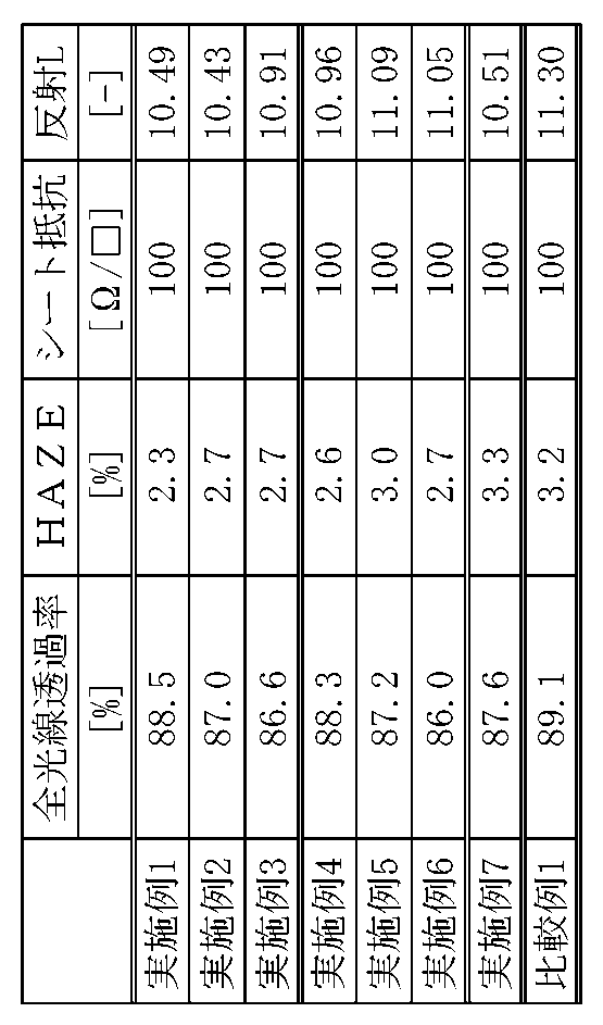
黒浮き防止層を導入することによって、シート抵抗の変化を完全に抑制しつつ、反射L値を改善することが可能となり、より高コントラストな透明導電層(金属フィラー導電層)の作製ができた。
黒浮き防止層の光吸収材料としては、染料や炭素材料(カーボンナノチューブ)を使用することが可能である。これらの材料を組み合わせて用いた場合にも、単独で用いた場合と同様に高コントラスト化が可能である。
染料や炭素材料などの光吸収材料を透明導電層中に含有させると、導電性シートの導電性が損なわれてしまうが、染料や炭素材料などの光吸収材料を含む黒浮き防止層を別途設けることで、導電性シートの導電性を損なうことなくコントラストを向上させることができたと考えられる。
黒浮き防止層を導入することにより、金属フィラーで乱反射された光が黒浮き防止層で吸収されることで、導電性シートの導電性を損なうことなく、コントラストを向上できたものと考えられる。
(1)
基材と、
金属フィラーを含む透明導電層と、
光吸収材料を含む光透過層と
を備える透明導電体。
(2)
上記光吸収材料は、可視光線を吸収する(1)に記載の透明導電体。
(3)
上記光吸収材料は、可視光線を吸収する有色化合物である(1)に記載の透明導電体。
(4)
上記有色化合物は、染料である(3)に記載の透明導電体。
(5)
上記有色化合物は、発色団を有している(3)に記載の透明導電体。
(6)
上記光吸収材料は、炭素材料である(1)に記載の透明導電体。
(7)
可視光線に対する上記光透過層の透過率は、50%以上である(1)から(6)のいずれかに記載の透明導電体。
(8)
上記金属フィラーは、金属ワイヤーである(1)から(7)のいずれかに記載の透明導電体。
(9)
上記光透過層は、上記基材と上記透明導電層との間に設けられている(1)から(8)のいずれかに記載の透明導電体。
(10)
上記透明導電層は、透明電極である(1)から(9)のいずれかに記載の透明導電体。
(11)
上記透明導電層は、バインダをさらに含んでいる(1)から(10)のいずれかに記載の透明導電体。
(12)
金属フィラーを含む透明導電層と、
光吸収材料を含む光透過層と
を備える入力装置。
(13)
上記光透過層は、上記透明導電層よりも入力面に近い位置に設けられている(12)に記載の入力装置。
(14)
表示装置と入力装置とを備え、
上記入力装置は、
金属フィラーを含む透明導電層と、
光吸収材料を含む光透過層と
を備える表示装置。
(15)
上記光透過層は、上記透明導電層よりも入力面に近い位置に設けられている(14)に記載の表示装置。
(16)
基材と、
金属フィラーを含む透明導電層と、
光吸収材料を含む光透過層と
を備え、
上記金属フィラー表面の少なくとも一部が有素化合物により被覆されている透明導電体。
11 基材
12、14 透明導電層
13、15 黒浮き防止層
101、202、212、222、232 表示装置
102 情報入力装置
201 テレビ装置
211 ノート型パーソナルコンピュータ
221 携帯電話
231 タブレット型コンピュータ
Claims (16)
- 基材と、
金属フィラーを含む透明導電層と、
光吸収材料を含む光透過層と
を備える透明導電体。 - 上記光吸収材料は、可視光線を吸収する請求項1に記載の透明導電体。
- 上記光吸収材料は、可視光線を吸収する有色化合物である請求項1に記載の透明導電体。
- 上記有色化合物は、染料である請求項3に記載の透明導電体。
- 上記有色化合物は、発色団を有している請求項3に記載の透明導電体。
- 上記光吸収材料は、炭素材料である請求項1に記載の透明導電体。
- 可視光線に対する上記光透過層の透過率は、50%以上である請求項1~6のいずれかに記載の透明導電体。
- 上記金属フィラーは、金属ワイヤーである請求項1~7のいずれかに記載の透明導電体。
- 上記光透過層は、上記基材と上記透明導電層との間に設けられている請求項1~8のいずれかに記載の透明導電体。
- 上記透明導電層は、透明電極である請求項1~9のいずれかに記載の透明導電体。
- 上記透明導電層は、バインダをさらに含んでいる請求項1~10のいずれかに記載の透明導電体。
- 金属フィラーを含む透明導電層と、
光吸収材料を含む光透過層と
を備える入力装置。 - 上記光透過層は、上記透明導電層よりも入力面に近い位置に設けられている請求項12に記載の入力装置。
- 表示装置と入力装置とを備え、
上記入力装置は、
金属フィラーを含む透明導電層と、
光吸収材料を含む光透過層と
を備える表示装置。 - 上記光透過層は、上記透明導電層よりも入力面に近い位置に設けられている請求項14に記載の表示装置。
- 基材と、
金属フィラーを含む透明導電層と、
光吸収材料を含む光透過層と
を備え、
上記金属フィラー表面の少なくとも一部が有素化合物により被覆されている透明導電体。
Priority Applications (4)
| Application Number | Priority Date | Filing Date | Title |
|---|---|---|---|
| US14/423,584 US20150185890A1 (en) | 2012-08-31 | 2013-08-19 | Transparent conductor, input device and electronic apparatus |
| CN201380044837.XA CN104540678A (zh) | 2012-08-31 | 2013-08-19 | 透明导电体、输入装置和电子仪器 |
| KR1020157004781A KR20150048128A (ko) | 2012-08-31 | 2013-08-19 | 투명 도전체, 입력 장치 및 전자 기기 |
| HK15105503.2A HK1205098A1 (en) | 2012-08-31 | 2013-08-19 | Transparent conductor, input device and electronic equipment |
Applications Claiming Priority (2)
| Application Number | Priority Date | Filing Date | Title |
|---|---|---|---|
| JP2012-192604 | 2012-08-31 | ||
| JP2012192604A JP2014046622A (ja) | 2012-08-31 | 2012-08-31 | 透明導電体、入力装置および電子機器 |
Publications (1)
| Publication Number | Publication Date |
|---|---|
| WO2014034451A1 true WO2014034451A1 (ja) | 2014-03-06 |
Family
ID=50183266
Family Applications (1)
| Application Number | Title | Priority Date | Filing Date |
|---|---|---|---|
| PCT/JP2013/072046 Ceased WO2014034451A1 (ja) | 2012-08-31 | 2013-08-19 | 透明導電体、入力装置および電子機器 |
Country Status (7)
| Country | Link |
|---|---|
| US (1) | US20150185890A1 (ja) |
| JP (1) | JP2014046622A (ja) |
| KR (1) | KR20150048128A (ja) |
| CN (1) | CN104540678A (ja) |
| HK (1) | HK1205098A1 (ja) |
| TW (1) | TW201425034A (ja) |
| WO (1) | WO2014034451A1 (ja) |
Cited By (1)
| Publication number | Priority date | Publication date | Assignee | Title |
|---|---|---|---|---|
| CN106232345A (zh) * | 2014-04-22 | 2016-12-14 | 沙特基础工业全球技术有限公司 | 集成的柔性透明导电膜 |
Families Citing this family (19)
| Publication number | Priority date | Publication date | Assignee | Title |
|---|---|---|---|---|
| JP6074851B2 (ja) * | 2013-03-29 | 2017-02-08 | パナソニックIpマネジメント株式会社 | 導電性光学部材 |
| JP6366577B2 (ja) * | 2013-04-26 | 2018-08-01 | 昭和電工株式会社 | 導電パターンの製造方法及び導電パターン形成基板 |
| US20150242011A1 (en) * | 2014-02-27 | 2015-08-27 | J Touch Corporation | Touch-sensitive panel device and electrode structure therein |
| JP5841634B2 (ja) * | 2014-04-17 | 2016-01-13 | 介面光電股▲ふん▼有限公司 | 黒化塗料及びそれを用いた電極構造 |
| CN109976596A (zh) * | 2014-06-27 | 2019-07-05 | 宸盛光电有限公司 | 触控感应单元 |
| CN106661255A (zh) | 2014-08-07 | 2017-05-10 | 沙特基础工业全球技术有限公司 | 用于热成型应用的导电多层片材 |
| US9913368B2 (en) * | 2015-01-22 | 2018-03-06 | Carestream Health, Inc. | Nanowire security films |
| TWI567757B (zh) * | 2015-06-03 | 2017-01-21 | 財團法人紡織產業綜合研究所 | 導電組成物 |
| CN105810290A (zh) * | 2016-03-24 | 2016-07-27 | 浙江零维光伏科技有限公司 | 一种有机薄膜太阳能电池用导电浆料及其制备方法 |
| KR102556838B1 (ko) * | 2016-06-01 | 2023-07-19 | 삼성디스플레이 주식회사 | 터치 패널, 이를 포함하는 전자 장치, 및 터치 패널 제조 방법 |
| KR20180012098A (ko) * | 2016-07-26 | 2018-02-05 | 삼성에스디아이 주식회사 | 투명 도전체, 이의 제조방법 및 이를 포함하는 디스플레이 장치 |
| TWI608391B (zh) * | 2016-11-07 | 2017-12-11 | 鴻銳科技股份有限公司 | 觸控螢幕鏡面結構 |
| JP2018133331A (ja) * | 2017-02-15 | 2018-08-23 | デクセリアルズ株式会社 | 異方性導電接続構造体、異方性導電接続構造体の製造方法、異方性導電フィルム、及び異方性導電ペースト |
| KR102097610B1 (ko) | 2017-09-29 | 2020-04-06 | 주식회사 엘지화학 | 디스플레이 패널용 시인성 개선 필름 및 이를 포함하는 디스플레이 장치 |
| DE102019101765A1 (de) * | 2019-01-24 | 2020-07-30 | Bayerische Motoren Werke Aktiengesellschaft | Modul für eine Anzeige- und/oder Bedienvorrichtung, Anzeige- und/oder Bedienvorrichtung, Verfahren zur Herstellung eines Moduls und Fortbewegungsmittel |
| US12327661B2 (en) | 2020-03-17 | 2025-06-10 | Korea Institute Of Machinery & Materials | Transparent conductor including nanostructure and manufacturing method thereof |
| CN112037968B (zh) * | 2020-07-07 | 2024-12-06 | 天材创新材料科技(厦门)有限公司 | 透明导电薄膜 |
| TWI732630B (zh) * | 2020-07-17 | 2021-07-01 | 大陸商天材創新材料科技(廈門)有限公司 | 透明導電薄膜 |
| CN112530627B (zh) * | 2020-11-16 | 2022-08-23 | 苏州城邦达益材料科技有限公司 | 一种低雾度透明导电膜及其制备方法 |
Citations (9)
| Publication number | Priority date | Publication date | Assignee | Title |
|---|---|---|---|---|
| JP2002154177A (ja) * | 2000-11-20 | 2002-05-28 | Kanebo Ltd | 半透過積層板 |
| JP2009127092A (ja) * | 2007-11-26 | 2009-06-11 | Konica Minolta Holdings Inc | 金属ナノワイヤ、及び金属ナノワイヤを含む透明導電体 |
| JP2010108172A (ja) * | 2008-10-29 | 2010-05-13 | Kyocera Corp | タッチパネルおよびタッチパネル型表示装置 |
| JP2011029036A (ja) * | 2009-07-27 | 2011-02-10 | Panasonic Electric Works Co Ltd | 透明導電膜付き基材 |
| JP2012006377A (ja) * | 2010-05-28 | 2012-01-12 | Fujifilm Corp | 導電シートの製造方法及びタッチパネルの製造方法 |
| JP4893867B1 (ja) * | 2011-02-23 | 2012-03-07 | ソニー株式会社 | 透明導電膜、分散液、情報入力装置、および電子機器 |
| JP2012104710A (ja) * | 2010-11-11 | 2012-05-31 | Fujimori Kogyo Co Ltd | Fpc用電磁波シールド材 |
| JP2013105888A (ja) * | 2011-11-14 | 2013-05-30 | Fujimori Kogyo Co Ltd | Fpc用電磁波シールド材 |
| JP5224203B1 (ja) * | 2012-07-11 | 2013-07-03 | 大日本印刷株式会社 | タッチパネルセンサ、タッチパネル装置および表示装置 |
Family Cites Families (7)
| Publication number | Priority date | Publication date | Assignee | Title |
|---|---|---|---|---|
| JP4572023B2 (ja) * | 2000-07-11 | 2010-10-27 | 株式会社槌屋 | 着色導電ペーストおよびそれを用いる導電積層体とその製造方法 |
| JP2004345278A (ja) * | 2003-05-23 | 2004-12-09 | Sony Corp | 透明導電性基材、抵抗膜方式タッチパネルおよび表示素子 |
| JP4191698B2 (ja) * | 2005-03-31 | 2008-12-03 | Tdk株式会社 | 透明導電体 |
| JP2006310195A (ja) * | 2005-04-28 | 2006-11-09 | Tdk Corp | 透明導電体 |
| JP2008225338A (ja) * | 2007-03-15 | 2008-09-25 | Seiko Epson Corp | 電気光学装置およびその製造方法、電子機器 |
| JP2010048844A (ja) * | 2008-08-19 | 2010-03-04 | Toray Advanced Film Co Ltd | ディスプレイ用フィルター |
| JP2014048791A (ja) * | 2012-08-30 | 2014-03-17 | Dainippon Printing Co Ltd | タッチパネル用電極積層体、及びタッチパネル、並びに画像表示装置 |
-
2012
- 2012-08-31 JP JP2012192604A patent/JP2014046622A/ja active Pending
-
2013
- 2013-08-19 KR KR1020157004781A patent/KR20150048128A/ko not_active Withdrawn
- 2013-08-19 CN CN201380044837.XA patent/CN104540678A/zh active Pending
- 2013-08-19 WO PCT/JP2013/072046 patent/WO2014034451A1/ja not_active Ceased
- 2013-08-19 HK HK15105503.2A patent/HK1205098A1/xx unknown
- 2013-08-19 US US14/423,584 patent/US20150185890A1/en not_active Abandoned
- 2013-08-27 TW TW102130562A patent/TW201425034A/zh unknown
Patent Citations (9)
| Publication number | Priority date | Publication date | Assignee | Title |
|---|---|---|---|---|
| JP2002154177A (ja) * | 2000-11-20 | 2002-05-28 | Kanebo Ltd | 半透過積層板 |
| JP2009127092A (ja) * | 2007-11-26 | 2009-06-11 | Konica Minolta Holdings Inc | 金属ナノワイヤ、及び金属ナノワイヤを含む透明導電体 |
| JP2010108172A (ja) * | 2008-10-29 | 2010-05-13 | Kyocera Corp | タッチパネルおよびタッチパネル型表示装置 |
| JP2011029036A (ja) * | 2009-07-27 | 2011-02-10 | Panasonic Electric Works Co Ltd | 透明導電膜付き基材 |
| JP2012006377A (ja) * | 2010-05-28 | 2012-01-12 | Fujifilm Corp | 導電シートの製造方法及びタッチパネルの製造方法 |
| JP2012104710A (ja) * | 2010-11-11 | 2012-05-31 | Fujimori Kogyo Co Ltd | Fpc用電磁波シールド材 |
| JP4893867B1 (ja) * | 2011-02-23 | 2012-03-07 | ソニー株式会社 | 透明導電膜、分散液、情報入力装置、および電子機器 |
| JP2013105888A (ja) * | 2011-11-14 | 2013-05-30 | Fujimori Kogyo Co Ltd | Fpc用電磁波シールド材 |
| JP5224203B1 (ja) * | 2012-07-11 | 2013-07-03 | 大日本印刷株式会社 | タッチパネルセンサ、タッチパネル装置および表示装置 |
Cited By (2)
| Publication number | Priority date | Publication date | Assignee | Title |
|---|---|---|---|---|
| CN106232345A (zh) * | 2014-04-22 | 2016-12-14 | 沙特基础工业全球技术有限公司 | 集成的柔性透明导电膜 |
| US20170066225A1 (en) * | 2014-04-22 | 2017-03-09 | Sabic Global Technologies B.V. | Integrated flexible transparent conductive film |
Also Published As
| Publication number | Publication date |
|---|---|
| TW201425034A (zh) | 2014-07-01 |
| KR20150048128A (ko) | 2015-05-06 |
| CN104540678A (zh) | 2015-04-22 |
| HK1205098A1 (en) | 2015-12-11 |
| US20150185890A1 (en) | 2015-07-02 |
| JP2014046622A (ja) | 2014-03-17 |
Similar Documents
| Publication | Publication Date | Title |
|---|---|---|
| WO2014034451A1 (ja) | 透明導電体、入力装置および電子機器 | |
| JP6094270B2 (ja) | 透明導電膜、導電性素子、組成物、入力装置、表示装置および電子機器 | |
| JP4893867B1 (ja) | 透明導電膜、分散液、情報入力装置、および電子機器 | |
| JP6327870B2 (ja) | 金属ナノワイヤー、透明導電膜及びその製造方法、分散液、情報入力装置、並びに、電子機器 | |
| CN104145312B (zh) | 透明导电膜、导电性元件、组合物、有色自组织材料、输入装置、显示装置和电子设备 | |
| US10365750B2 (en) | Transparent conductive film and method for producing same, information input device, and electronic device | |
| JP2017050251A (ja) | 分散液、透明導電膜、入力装置及び有機el照明装置 | |
| JP2014241353A (ja) | 帯域選択透明シールドと、帯域選択透明シールドの製造方法、これを用いた表示デバイスと、表示機器 | |
| WO2014034468A1 (ja) | 透明導電性素子およびその製造方法、入力装置、電子機器、ならびに導電部の形成方法 | |
| JP2014241354A (ja) | 帯域選択偏光シールドと、帯域選択偏光シールドの製造方法、表示デバイスと、表示機器 | |
| JP2017065257A (ja) | 光透過性導電フィルム | |
| HK1189088A (en) | Transparent electroconductive film, information input device, and electronic instrument | |
| JP2016104908A (ja) | 金属ナノワイヤー、透明導電膜及びその製造方法、分散液、情報入力装置、並びに、電子機器 |
Legal Events
| Date | Code | Title | Description |
|---|---|---|---|
| 121 | Ep: the epo has been informed by wipo that ep was designated in this application |
Ref document number: 13833200 Country of ref document: EP Kind code of ref document: A1 |
|
| DPE1 | Request for preliminary examination filed after expiration of 19th month from priority date (pct application filed from 20040101) | ||
| WWE | Wipo information: entry into national phase |
Ref document number: 14423584 Country of ref document: US |
|
| ENP | Entry into the national phase |
Ref document number: 20157004781 Country of ref document: KR Kind code of ref document: A |
|
| NENP | Non-entry into the national phase |
Ref country code: DE |
|
| 122 | Ep: pct application non-entry in european phase |
Ref document number: 13833200 Country of ref document: EP Kind code of ref document: A1 |