WO2014034341A1 - 有機エレクトロルミネッセンス素子 - Google Patents
有機エレクトロルミネッセンス素子 Download PDFInfo
- Publication number
- WO2014034341A1 WO2014034341A1 PCT/JP2013/070355 JP2013070355W WO2014034341A1 WO 2014034341 A1 WO2014034341 A1 WO 2014034341A1 JP 2013070355 W JP2013070355 W JP 2013070355W WO 2014034341 A1 WO2014034341 A1 WO 2014034341A1
- Authority
- WO
- WIPO (PCT)
- Prior art keywords
- group
- layer
- organic
- ring
- light emitting
- Prior art date
- Legal status (The legal status is an assumption and is not a legal conclusion. Google has not performed a legal analysis and makes no representation as to the accuracy of the status listed.)
- Ceased
Links
Images

Classifications
-
- H—ELECTRICITY
- H10—SEMICONDUCTOR DEVICES; ELECTRIC SOLID-STATE DEVICES NOT OTHERWISE PROVIDED FOR
- H10K—ORGANIC ELECTRIC SOLID-STATE DEVICES
- H10K50/00—Organic light-emitting devices
- H10K50/10—OLEDs or polymer light-emitting diodes [PLED]
- H10K50/11—OLEDs or polymer light-emitting diodes [PLED] characterised by the electroluminescent [EL] layers
- H10K50/125—OLEDs or polymer light-emitting diodes [PLED] characterised by the electroluminescent [EL] layers specially adapted for multicolour light emission, e.g. for emitting white light
- H10K50/13—OLEDs or polymer light-emitting diodes [PLED] characterised by the electroluminescent [EL] layers specially adapted for multicolour light emission, e.g. for emitting white light comprising stacked EL layers within one EL unit
- H10K50/131—OLEDs or polymer light-emitting diodes [PLED] characterised by the electroluminescent [EL] layers specially adapted for multicolour light emission, e.g. for emitting white light comprising stacked EL layers within one EL unit with spacer layers between the electroluminescent layers
-
- H—ELECTRICITY
- H10—SEMICONDUCTOR DEVICES; ELECTRIC SOLID-STATE DEVICES NOT OTHERWISE PROVIDED FOR
- H10K—ORGANIC ELECTRIC SOLID-STATE DEVICES
- H10K50/00—Organic light-emitting devices
- H10K50/10—OLEDs or polymer light-emitting diodes [PLED]
- H10K50/19—Tandem OLEDs
Definitions
- the present invention relates to an organic electroluminescence element.
- an organic electroluminescence element basically has a layer structure composed of an anode / an organic light emitting layer / a cathode, and a layer such as a hole injection layer, a hole transport layer, an electron transport layer, and an electron injection layer. Is appropriately provided. It is known that an organic EL element having such a configuration generally has a trade-off relationship between light emission current efficiency and drive life. Therefore, in order to improve the trade-off relationship, studies have been made from various viewpoints such as organic materials, organic layer configurations, element driving methods, and the like.
- a light emitting functional layer group composed of one or more layers including at least a light emitting layer composed of an organic material is defined as one light emitting unit.
- a so-called tandem structure that can achieve a long life while maintaining the light emission current efficiency by stacking a plurality of light emitting units via an intermediate layer, or can significantly increase the light emission current efficiency without significantly deteriorating the drive life Has been proposed.
- Patent Document 1 discloses a configuration having two conductive layers between OLED layers, and specifically discloses a laminated structure of an Mg—Ag alloy film and an ITO film.
- Patent Document 2 discloses an intermediate conductive layer composed of at least two layers, specifically, a laminate of an 8 nm thick Mg—Ag alloy film and a 10 nm thick In—Zn—O conductive film. The structure and the like are disclosed.
- Patent Document 3 discloses a technique for expressing conductivity by doping an acceptor or a donor into a floating conductive thin film layer containing an organic compound.
- Patent Document 4 discloses an intermediate layer formed by stacking organic layers doped with an acceptor and a donor.
- Patent Document 6 discloses a configuration in which a metal layer (internal electrode) having a work function of 4.5 eV or less is inserted between light emitting units, and “Patent Document 7” also has a similar configuration in the embodiment. It is disclosed.
- Patent Document 1 In the configurations disclosed in “Patent Document 1” and “Patent Document 2”, it is necessary to laminate two conductive layers, and ITO, In—Zn—O, which is disclosed as an actual mode.
- the film needs to be formed by a sputtering method, and generally has a heavy load in terms of production efficiency because it is different from a film formation process of an organic EL element formed by a vapor deposition method or a coating method.
- damage to the organic film cannot be ignored.
- Patent Document 3 The method using a doping layer described in “Patent Document 3”, “Patent Document 4”, and “Patent Document 5” has a load on the process surface compared to “Patent Document 1” and “Patent Document 2”.
- securing production stability becomes an issue, and there is an increased risk of performance deterioration due to diffusion of the doping material into each layer of the light emitting unit.
- Patent Document 6 The configuration in which one metal layer disclosed in “Patent Document 6” and “Patent Document 7” is inserted between the light emitting units is relatively a process compared to “Patent Document 1” and “Patent Document 2”. Although the load on the surface is small and there is little concern about performance fluctuations due to material diffusion, according to the study by the present inventors, it has been found that there are still problems to be improved. Specifically, in the example of “Patent Document 6”, a structure with a film thickness of 6 nm using Al (work function of about 4.3 eV) is disclosed. However, since only the Al layer has a high driving voltage, An electron injecting layer is required adjacent to the anode side of the layer.
- the present invention has been made in view of the above-mentioned problems and situations, and its solution is from a laminated structure of a plurality of light emitting units, which is excellent in low drive voltage, high light emission efficiency, storage stability performance and improved productivity.
- An organic EL element that further exhibits white light emission is provided.
- the present inventor has at least one intermediate metal layer and at least two light-emitting units between the anode and the cathode, An organic EL element comprising an intermediate metal layer disposed between two light emitting units, the intermediate metal layer being made of a metal having a work function of 3.0 eV or less, and a film thickness of 0.6 to 5 nm
- the inventors have found that the above problems can be improved and have reached the present invention.
- An organic electroluminescent element having at least one intermediate metal layer and at least two light emitting units between an anode and a cathode, wherein the intermediate metal layer is disposed between the two light emitting units. And The organic electroluminescent element, wherein the intermediate metal layer is made of a metal having a work function of 3.0 eV or less and has a film thickness of 0.6 to 5 nm.
- an organic EL element having a laminated structure of a plurality of light-emitting units, excellent in low driving voltage, high luminous efficiency, storage stability performance, and improved productivity, and further organic EL exhibiting white light emission.
- An element can be provided.
- the organic EL device of the present invention has at least one intermediate metal layer and at least two light emitting units between an anode and a cathode, and the intermediate metal layer is disposed between the two light emitting units.
- the metal layer is made of a metal having a work function of 3.0 eV or less and has a film thickness of 0.6 to 5 nm.
- At least one surface is formed as a non-flat surface rather than a case where the intermediate metal layer has a completely flat surface. If one surface of the intermediate metal layer is a non-flat surface, it is difficult for current to flow in the in-plane direction, and current concentration on the thin film portion caused by unevenness of the organic layer thickness due to variations in the substrate surface thickness, etc. Further, it is possible to suppress the occurrence of a short circuit failure or the like associated therewith.
- the layer adjacent to the anode side of the intermediate metal layer is a layer formed by forming a single organic compound, so that the production process of single and organic material film formation is easy and process control.
- the layer structure of a laminated body, the constituent material of each layer, and the other adjacent to the intermediate metal layer side of a laminated body it is preferable from the viewpoint of production efficiency and stability that the layer structure of the light emitting unit or other laminate and the constituent material of each layer are the same except for the light emitting layer.
- the phosphorescent light emitting material and the fluorescent light emitting material are not mixed, and only the phosphorescent light emitting material or only the fluorescent light emitting material is used to suppress the loss of light emission efficiency. Preferred above. This is because when phosphorescent light emitting material and fluorescent light emitting material are mixed in the same light emitting unit, energy transfer between the phosphorescent light emitting material and the fluorescent light emitting material and loss of light emission efficiency due to quenching are likely to occur.
- the organic EL element of the present invention can be suitably included in a lighting device.
- ⁇ is used to mean that the numerical values described before and after it are included as a lower limit value and an upper limit value.
- the number of light emitting units is not particularly limited as long as it is 2 or more. However, in view of production efficiency, 2 to 10 is preferable, and 2 to 4 is more preferable.
- the number of light emitting units is N (N is an integer of 2 or more)
- the number of intermediate metal layers of the present invention is N-1.
- each layer for example, a vacuum deposition method, a spin coating method, a casting method, an LB method (Langmuir-Blodget method), an ink jet method, a spray method, a printing method, a slot type coater method, etc.
- the film can be formed by a known thin film forming method.
- a phosphorescent light emitting material and a fluorescent light emitting material may be mixed in the light emitting layer in the light emitting unit, but it is preferable that the phosphor layer is preferably composed only of the phosphorescent light emitting material or the fluorescent light emitting material.
- the fluorescent light emitting layer and the phosphorescent light emitting layer are preferably a host or dopant type light emitting layer.
- the light emission dopant contained in a light emitting layer may be contained with the uniform density
- each light emitting unit can be used in combination with different ones, but except for the light emitting layer constituting the light emitting unit, it is preferable that the same layer and material are used, Furthermore, it is preferable that the number of light emitting layers is the same. In this case, it is possible to reduce the number of materials used in production, and there are advantages in terms of cost and quality control. Furthermore, in the case of a vapor deposition process, it is easy to make the film forming chamber common to each light emitting unit. Can also enjoy. For the above reasons, when the white light emitting units are stacked, it is more preferable that the configuration and materials of all layers including the light emitting layer are the same.
- an organic EL element that emits white light can be obtained by providing a blue light-emitting unit and a light-emitting unit that emits a complementary green, yellow-green, yellow, or orange light-emitting color.
- the “complementary color” relationship is a relationship between colors that become achromatic when mixed. That is, white light emission can be obtained by mixing light emission of substances emitting light of complementary colors.
- a layer exhibiting green and red light-emitting colors is provided in any light-emitting unit. It is preferable.
- blue, green, and red light-emitting materials can be mixed in one light-emitting layer and provided in the light-emitting unit as a light-emitting layer that emits white light.
- the light emission color of the organic EL device of the present invention and the compound according to the present invention is shown in FIG. 4.16 on page 108 of “New Color Science Handbook” (edited by the Japan Color Society, University of Tokyo Press, 1985). It is determined by the color when the result measured with a total CS-1000 (manufactured by Konica Minolta Sensing) is applied to the CIE chromaticity coordinates.
- CS-1000 manufactured by Konica Minolta Sensing
- white light light whose deviation Duv from the black body radiation locus of the light color is within the range of ⁇ 20 to +20 within the range of the correlated color temperature of 2500 to 7500 K is referred to as white light.
- each light emitting layer included in each light emitting unit in the present invention is not particularly limited, but it prevents the homogeneity of the film to be formed and the application of unnecessary high voltage during light emission, and From the viewpoint of improving the stability of the emission color with respect to the driving current, it is preferably adjusted within the range of 5 to 200 nm, more preferably within the range of 10 to 100 nm.
- the intermediate metal layer according to the present invention is disposed and formed between two light emitting units.
- the intermediate metal layer may be formed in a state in which a metal material is hardly formed on a partial fine region thereof, a so-called pinhole is formed, or may be formed in a net shape in the in-plane direction.
- the intermediate metal layer forming portion may be formed in an island shape (a spot shape).
- the intermediate metal layer of the present invention a metal having a work function of 3.0 eV or less is used.
- Materials used for the intermediate metal layer include calcium (work function 2.87 eV, melting point 1112.2 K), lithium (2.9 eV, 453.7 K), sodium (2.75 eV, 371 K), potassium ( 2.3 eV, 336.9 K), cesium (2.14 eV, 301.6 K), rubidium (2.16 eV, 312.1 K), barium (2.7 eV, 998.2 K), Strontium (2.59 eV, 1042.2 K) is mentioned above.
- the melting point at normal pressure is 400 K or more, and lithium, calcium, and barium are less likely to impair the performance of the organic EL device in a high temperature environment. Strontium is preferred.
- the electron injection barrier from the light emitting unit located on the cathode side to the light emitting unit located on the anode side with respect to the intermediate metal layer is large, and the driving voltage of the organic EL element becomes high.
- the layer adjacent to the cathode side of the intermediate metal layer is not subjected to so-called n-type doping and is formed as a single organic compound layer having a simpler productive structure, a larger problem arises.
- the film thickness of the intermediate metal layer of the present invention is in the range of 0.6 to 5 nm.
- the thickness is preferably 0.8 to 3 nm, and more preferably 0.8 to 2 nm.
- the thickness of the intermediate metal layer is larger than 5 nm, the efficiency of the organic EL element is reduced due to the light absorption of the metal material used, and the storage stability and drive stability are deteriorated.
- the reason why the stability deteriorates is not clear, but if the film thickness is thick, the electrical characteristics of the intermediate metal layer become closer to the characteristics as the metal bulk, so that the conductivity of the film increases, and the in-plane direction of the film increases. It is conceivable that the conductivity increases, the current concentration on the thin film portion caused by the film thickness unevenness of the organic layer due to the in-plane variation of the film thickness, etc., and the occurrence of a short circuit failure accompanying the current concentration are accelerated.
- the film thickness of the intermediate metal layer is less than 0.6 nm
- the performance stability of the organic EL element in particular, the performance fluctuation at a relatively early stage after the element is produced. It turned out to be big.
- the cause of the deterioration of the initial stability is not clear, but if the film thickness is excessively thin and consists of a metal film with a thickness of several angstroms or a metal lump with a cluster diameter, its physical and chemical
- the stability of the metal film or metal lump is greatly different from the bulk metal state due to chemical reactions including oxidation-reduction reactions with adjacent layer materials, heat, and interaction with the charges associated with driving the device.
- the “film thickness of the intermediate metal layer” in the present invention is defined as the “average film thickness” obtained by dividing the film formation weight per unit area of the intermediate metal layer by the density of the material. Therefore, a certain part of the intermediate metal layer may be thicker than the “average film thickness” or may be thinner.
- Patent Document 6 discloses a configuration using “a single-layer internal electrode made of a material selected from the group consisting of a metal having a work function of 4.5 eV or less, an alloy thereof, and an oxide thereof”.
- the configuration specifically shown in the examples is only a configuration using Al (work function 4.28 eV) with a film thickness of 6 nm for the internal electrode.
- the work function 3. Compared with the present invention using a metal of 0 eV or less, the driving voltage is remarkably high. In particular, when the layer adjacent to the anode side of the intermediate metal layer is composed of a single organic compound, the difference is remarkable.
- Patent Document 7 discloses a configuration using a Li layer having a film thickness of 0.3 nm as the metal layer. As shown in the above description and the examples described later, an intermediate metal is used. When the thickness of the layer is as thin as about 0.3 nm, it has been found that the fluctuation in performance is large in the initial driving of the organic EL element or in a relatively short period after the element is manufactured.
- At least the light emitting unit side surfaces of the intermediate metal layer have at least a completely flat surface.
- One of the surfaces is preferably formed as a non-flat surface.
- the intermediate metal layer having a non-flat surface means that the shape of the intermediate metal layer in the in-plane direction is a net or an island.
- the layer adjacent to the anode side of the intermediate metal layer is preferably a layer formed by forming a single organic compound.
- the production process is simplified and process management is facilitated, and the risk of performance fluctuation due to the use of multiple materials can be avoided, as well as better long-term or high-temperature storage stability and long-term drive stability. Since it is obtained, it is preferable.
- the layer adjacent to the intermediate metal layer is used to transfer charge from each light emitting unit to / from each light emitting unit via the intermediate metal layer between the light emitting unit located on the cathode side and the light emitting unit located on the anode side. It is desirable to have a function that facilitates injection.
- a layer having such a function for example, a charge transporting organic material and an inorganic material capable of oxidizing or reducing the organic material or forming a charge transfer complex with the organic material in order to enhance charge transporting properties.
- Patent Document 6 a layer made of LiF is provided as a layer adjacent to the anode side of the Al internal electrode. It has been found that the method of providing a thin layer of these doping materials (alkali or alkaline earth compound) impairs storage stability and driving stability in addition to the above-mentioned disadvantages in the production process.
- Phosphorescent host compound used in the present invention is not particularly limited in terms of structure, but is typically a carbazole derivative, a triarylamine derivative, an aromatic borane derivative, or a nitrogen-containing heterocyclic ring.
- Compounds having a basic skeleton such as compounds, thiophene derivatives, furan derivatives, oligoarylene compounds, or carboline derivatives or diazacarbazole derivatives (Here, diazacarbazole derivatives are hydrocarbon rings constituting the carboline ring of carboline derivatives. In which at least one carbon atom is substituted with a nitrogen atom).
- the phosphorescent host compound may be used alone or in combination of two or more.
- a compound represented by the following general formula (a) is preferable.
- X represents NR ′, O, S, CR′R ′′ or SiR′R ′′, and R ′ and R ′′ each represents a hydrogen atom or a substituent.
- Ar represents Represents an aromatic ring.
- n represents an integer of 0 to 8.
- the substituents represented by R ′ and R ′′ are each an alkyl group (for example, methyl group, ethyl group, propyl group, isopropyl group, tert-butyl group, pentyl group).
- substituents may be further substituted with the above substituents.
- a plurality of these substituents may be bonded to each other to form a ring.
- preferred “X” is NR ′ or O, and R ′ is particularly preferably an aromatic hydrocarbon group or an aromatic heterocyclic group.
- examples of the aromatic ring represented by “Ar” include an aromatic hydrocarbon ring and an aromatic heterocyclic ring.
- the aromatic ring may be either a single ring or a condensed ring, and may be unsubstituted or may have a substituent as described later.
- the aromatic hydrocarbon ring represented by “Ar” includes a benzene ring, biphenyl ring, naphthalene ring, azulene ring, anthracene ring, phenanthrene ring, pyrene ring, chrysene ring, naphthacene ring, triphenylene Ring, o-terphenyl ring, m-terphenyl ring, p-terphenyl ring, acenaphthene ring, coronene ring, fluorene ring, fluoranthrene ring, naphthacene ring, pentacene ring, perylene ring, pentaphen ring, picene ring, pyrene Ring, pyranthrene ring, anthraanthrene ring and the like. These rings may further have a substituent.
- examples of the aromatic heterocycle represented by “Ar” include a furan ring, dibenzofuran ring, thiophene ring, oxazole ring, pyrrole ring, pyridine ring, pyridazine ring, pyrimidine ring, pyrazine ring, Triazine ring, benzimidazole ring, oxadiazole ring, triazole ring, imidazole ring, pyrazole ring, thiazole ring, indole ring, indazole ring, benzimidazole ring, benzothiazole ring, benzoxazole ring, quinoxaline ring, quinazoline ring, cinnoline ring , Quinoline ring, isoquinoline ring, phthalazine ring, naphthyridine ring, carbazole ring, carboline ring, diazacarbazole ring (
- the aromatic ring represented by “Ar” is preferably a carbazole ring, a carboline ring, a dibenzofuran ring, or a benzene ring, and particularly preferably used is a carbazole.
- a ring, a carboline ring, and a benzene ring is preferable, and a benzene ring having a carbazolyl group is particularly preferable.
- the aromatic ring represented by “Ar” is preferably a condensed ring having three or more rings, as shown below, and is an aromatic in which three or more rings are condensed.
- the hydrocarbon condensed ring include naphthacene ring, anthracene ring, tetracene ring, pentacene ring, hexacene ring, phenanthrene ring, pyrene ring, benzopyrene ring, benzoazulene ring, chrysene ring, benzochrysene ring, acenaphthene ring, acenaphthylene Ring, triphenylene ring, coronene ring, benzocoronene ring, hexabenzocoronene ring, fluorene ring, benzofluorene ring, fluoranthene ring, perylene ring, naphthoperylene ring,
- aromatic heterocycle condensed with three or more rings include an acridine ring, a benzoquinoline ring, a carbazole ring, a carboline ring, a phenazine ring, a phenanthridine ring, a phenanthroline ring, a carboline ring, a cyclazine ring, Kindin ring, tepenidine ring, quinindrin ring, triphenodithiazine ring, triphenodioxazine ring, phenanthrazine ring, anthrazine ring, perimidine ring, diazacarbazole ring (any one of the carbon atoms constituting the carboline ring is a nitrogen atom Phenanthroline ring, dibenzofuran ring, dibenzothiophene ring, naphthofuran ring, naphthothiophene ring, benzodifuran ring, benzod
- n represents an integer of 0 to 8, preferably an integer of 0 to 2, particularly 1 or 2 when “X” is O or S. Is preferred.
- the phosphorescent host compound used in the present invention may be a low molecular compound or a high molecular compound having a repeating unit, and a low molecular compound having a polymerizable group such as a vinyl group or an epoxy group (evaporation polymerizable light emitting host). But you can.
- the phosphorescent host compound a compound having a hole transporting ability and an electron transporting ability, which prevents emission of light from being increased in wavelength and has a high Tg (glass transition temperature) is preferable.
- a compound having a glass transition point of 90 ° C. or higher is preferable, and a compound having a glass transition temperature of 130 ° C. or higher is preferable because excellent characteristics can be obtained.
- the glass transition point (Tg) is a value determined by a method based on JIS K 7121 using DSC (Differential Scanning Colorimetry).
- the phosphorescent host compound when a plurality of phosphorescent light emitting layers are provided, the phosphorescent host compound may be different for each light emitting layer, but the same compound is preferable in terms of production efficiency and process management.
- the phosphorescent host compound preferably has a lowest excited triplet energy (T 1 ) larger than 2.7 eV because higher luminous efficiency can be obtained.
- the lowest excited triplet energy as used in the present invention refers to the peak energy of an emission band corresponding to the transition between the lowest vibrational bands of a phosphorescence emission spectrum observed at a liquid nitrogen temperature after dissolving a host compound in a solvent.
- the phosphorescence emission dopant which can be used for this invention can be selected from a well-known thing. For example, it can be selected from complex compounds containing metals of Group 8 to Group 10 in the periodic table of elements, preferably iridium compounds, osmium compounds, platinum compounds (platinum complex compounds), or rare earth complexes. Of these, iridium compounds are the most preferred.
- a phosphorescent light emitting material is preferable as a light emitting body responsible for light emission in at least the green, yellow, and red regions.
- Ra represents a hydrogen atom, an aliphatic group, an aromatic group or a heterocyclic group
- Rb and Rc each represents a hydrogen atom or a substituent
- A1 represents an aromatic Represents a residue necessary to form an aromatic ring or an aromatic heterocyclic ring
- M represents Ir or Pt.
- Ra represents a hydrogen atom, an aliphatic group, an aromatic group or a heterocyclic group
- Rb”, “Rc”, “Rb 1 ” and “Rc 1 ” are each a hydrogen atom or Represents a substituent
- A1 represents a residue necessary to form an aromatic ring or an aromatic heterocycle
- M represents Ir or Pt.
- Ra represents a hydrogen atom, an aliphatic group, an aromatic group or a heterocyclic group
- Rb and Rc each represents a hydrogen atom or a substituent
- A1 represents an aromatic Represents a residue necessary to form an aromatic ring or an aromatic heterocyclic ring
- M represents Ir or Pt.
- the aliphatic group represented by “Ra” is an alkyl group (for example, methyl group, ethyl group, propyl group, butyl group, pentyl group, isopentyl group, 2-ethyl group).
- -Hexyl group octyl group, undecyl group, dodecyl group, tetradecyl group
- cycloalkyl group for example, cyclopentyl group, cyclohexyl group
- aromatic groups include, for example, phenyl group, tolyl group, azulenyl group, Anthranyl group, phenanthryl group, pyrenyl group, chrysenyl group, naphthacenyl group, o-terphenyl group, m-terphenyl group, p-terphenyl group, acenaphthenyl group, coronenyl group, fluorenyl group, perylenyl group, etc.
- ring group examples include pyrrolyl group, indolyl group, furyl group, thienyl group, Midazolyl, pyrazolyl, indolizinyl, quinolinyl, carbazolyl, indolinyl, thiazolyl, pyridyl, pyridazinyl, thiadiazinyl, oxadiazolyl, benzoquinolinyl, thiadiazolyl, pyrrolothiazolyl, pyrrolopyridazinyl, tetrazolyl
- a group, an oxazolyl group, a chromanyl group and the like, and these groups each may have a substituent.
- the substituent represented by “Rb”, “Rc”, “Rb 1 ”, “Rc 1 ” is an alkyl group (for example, a methyl group, an ethyl group, a propyl group).
- the aromatic ring represented by “A1” includes a benzene ring, biphenyl ring, naphthalene ring, azulene ring, anthracene ring, phenanthrene ring, pyrene ring, chrysene ring, naphthacene ring , Triphenylene ring, o-terphenyl ring, m-terphenyl ring, p-terphenyl ring, acenaphthene ring, coronene ring, fluorene ring, fluoranthrene ring, naphthacene ring, pentacene ring, perylene ring, pentaphen ring, picene ring , Pyrene ring, pyranthrene ring, anthraanthrene ring, etc., and aromatic heterocycle includes furan ring, thiophene ring, pyridine ring
- M represents Ir or Pt, and Ir is particularly preferable.
- the structures of the general formulas (A) to (C) are partial structures, and a ligand corresponding to the valence of the central metal is necessary for the structure itself to be a light-emitting dopant of a completed structure.
- halogen for example, fluorine atom, chlorine atom, bromine atom or iodine atom
- aryl group for example, phenyl group, p-chlorophenyl group, mesityl group, tolyl group, xylyl group, biphenyl group, naphthyl group) , Anthryl group, phenanthryl group, etc.
- alkyl group eg, methyl group, ethyl group, isopropyl group, hydroxyethyl group, methoxymethyl group, trifluoromethyl group, t-butyl group, etc.
- alkyloxy group for example, fluorine atom, chlorine atom, bromine atom or iodine atom
- a tris body having a completed structure with three partial structures of the general formulas (A) to (C) is preferable.
- Fluorescent light emitting dopant also called fluorescent dopant, fluorescent light emitter, etc.
- Fluorescent light emitting dopants include coumarin dyes, pyran dyes, cyanine dyes, croconium dyes, squalium dyes, oxobenzanthracene dyes, fluorescein dyes, rhodamine dyes, pyrylium dyes, perylene dyes, stilbene dyes Examples thereof include dyes, polythiophene dyes, and rare earth complex phosphors.
- injection layer hole injection layer, electron injection layer
- the injection layer may be provided as necessary, and may be provided between the anode or intermediate metal layer and the light emitting layer or hole transport layer, and between the cathode or intermediate metal layer and the light emitting layer or electron transport layer. Good.
- the injection layer is a layer provided between the electrode and the intermediate metal layer and the organic layer for lowering the driving voltage and improving the light emission luminance.
- the organic EL element and its industrialization front line June 30, 1998, N. The details are described in Chapter 2, “Electrode Materials” (pages 123 to 166) of Volume 2 of TS Co., Ltd.).
- hole injection layer anode buffer layer
- JP-A-9-45479 JP-A-9-260062, JP-A-8-288069, and the like.
- Specific examples thereof include copper phthalocyanine.
- Phthalocyanine buffer layer typified by (1), oxide buffer layer typified by vanadium oxide, amorphous carbon buffer layer, polymer buffer layer using a conductive polymer such as polyaniline (emeraldine) or polythiophene, and the like. It is also preferable to use the materials described in JP-T-2003-519432.
- the hole injection layer (or the layer adjacent to the cathode side of the anode and intermediate metal layer) may be a mixture of a plurality of materials.
- the hole injection layer is made of a single organic compound. It is preferably formed by filming. This is not preferable when a plurality of materials are mixed and used because the risk of performance fluctuations due to fluctuations in the mixing ratio during production, for example, concentration fluctuations in the surface of the film-forming substrate is increased.
- the thickness of the hole injection layer is not particularly limited, but is usually in the range of about 0.1 to 100 nm, preferably in the range of 1 to 30 nm.
- Suitable materials for the electron injection layer include alkali metals, alkaline earth metals, and compounds thereof having a work function of 3 eV or less in the electron injection layer provided between the electron transport layer and the cathode.
- Specific examples of the alkali metal compound include potassium fluoride, lithium fluoride, sodium fluoride, cesium fluoride, lithium oxide, lithium quinoline complex, cesium carbonate and the like, and lithium fluoride and cesium fluoride are preferable.
- the film thickness of the electron injection layer is not particularly limited, but is usually in the range of about 0.1 to 10 nm, preferably in the range of 0.1 to 2 nm.
- ⁇ Blocking layer hole blocking layer, electron blocking layer>
- the blocking layer is provided as necessary. For example, it is described in JP-A Nos. 11-204258 and 11-204359, and “Organic EL elements and the forefront of industrialization (published by NTT Corporation on Nov. 30, 1998)”. There is a hole blocking (hole blocking) layer.
- the hole blocking layer has a function of an electron transport layer in a broad sense, and is made of a hole blocking material that has a function of transporting electrons and has a remarkably small ability to transport holes. The probability of recombination of electrons and holes can be improved by blocking. Moreover, the structure of the electron carrying layer mentioned later can be used as a hole-blocking layer as needed.
- the hole blocking layer provided in the organic EL device of the present invention is preferably provided adjacent to the light emitting layer.
- the electron blocking layer has a function of a hole transport layer in a broad sense, and is made of a material that has a function of transporting holes and has an extremely small ability to transport electrons, and transports electrons while transporting holes. By blocking, the recombination probability of electrons and holes can be improved. Moreover, the structure of the positive hole transport layer mentioned later can be used as an electron blocking layer as needed.
- the film thickness of the hole blocking layer and the electron blocking layer according to the present invention is preferably in the range of 3 to 100 nm, and more preferably in the range of 5 to 30 nm.
- the hole transport layer is made of a hole transport material having a function of transporting holes, and in a broad sense, a hole injection layer and an electron blocking layer are also included in the hole transport layer.
- the hole transport layer can be provided as a single layer or a plurality of layers.
- the hole transport material has any one of hole injection or transport and electron barrier properties, and may be either organic or inorganic.
- triazole derivatives oxadiazole derivatives, imidazole derivatives, polyarylalkane derivatives, pyrazoline derivatives and pyrazolone derivatives, phenylenediamine derivatives, arylamine derivatives, amino-substituted chalcone derivatives, oxazole derivatives, styrylanthracene derivatives, fluorenone derivatives, hydrazone derivatives
- Examples thereof include stilbene derivatives, silazane derivatives, aniline copolymers, and conductive polymer oligomers, particularly thiophene oligomers.
- the above-mentioned materials can be used as the hole transport material, and it is further preferable to use a porphyrin compound, an aromatic tertiary amine compound and a styrylamine compound, particularly an aromatic tertiary amine compound.
- aromatic tertiary amine compounds and styrylamine compounds include N, N, N ′, N′-tetraphenyl-4,4′-diaminophenyl, N, N′-diphenyl-N, N′— Bis (3-methylphenyl)-[1,1'-biphenyl] -4,4'-diamine (TPD), 2,2-bis (4-di-p-tolylaminophenyl) propane, 1,1-bis (4-di-p-tolylaminophenyl) cyclohexane, N, N, N ′, N′-tetra-p-tolyl-4,4′-diaminobiphenyl, 1,1-bis (4-di-p-tolyl) Aminophenyl) -4-phenylcyclohexane, bis (4-dimethylamino-2-methylphenyl) phenylmethane, bis (4-di-p-tolylaminoph
- a polymer material in which these materials are introduced into a polymer chain or these materials are used as a polymer main chain can also be used.
- inorganic compounds such as p-type-Si and p-type-SiC can also be used as the hole injection material and the hole transport material.
- the thickness of the hole transport layer is not particularly limited, but is usually in the range of about 5 nm to 5 ⁇ m, preferably in the range of 5 to 200 nm.
- the hole transport layer may have a single layer structure composed of one or more of the above materials.
- the electron transport layer is made of a material having a function of transporting electrons.
- the electron transport layer can be provided as a single layer or a plurality of layers.
- the electron transporting material used for the electron transporting layer only needs to have a function of transmitting electrons injected through the cathode or the intermediate metal layer to the light emitting layer, and any conventionally known compound may be used.
- any conventionally known compound may be used.
- nitro-substituted fluorene derivatives, diphenylquinone derivatives, thiopyrandioxide derivatives, bipyridyl derivatives, fluorenylidenemethane derivatives, carbodiimides, anthraquinodimethane and anthrone derivatives, oxadiazole derivatives, etc. Can be mentioned.
- a thiadiazole derivative in which the oxygen atom of the oxadiazole ring is substituted with a sulfur atom, and a quinoxaline derivative having a quinoxaline ring known as an electron withdrawing group can also be used as an electron transport material.
- a polymer material in which these materials are introduced into a polymer chain or these materials are used as a polymer main chain can also be used.
- an electron transport layer is provided adjacent to the intermediate metal layer, it is preferably a compound that includes a pyridine ring in its structure.
- metal complexes of 8-quinolinol derivatives such as tris (8-quinolinol) aluminum (Alq), tris (5,7-dichloro-8-quinolinol) aluminum, tris (5,7-dibromo-8-quinolinol) aluminum Tris (2-methyl-8-quinolinol) aluminum, tris (5-methyl-8-quinolinol) aluminum, bis (8-quinolinol) zinc (Znq), and the like, and the central metals of these metal complexes are In, Mg, Metal complexes replaced with Cu, Ca, Sn, Ga or Pb can also be used as the electron transport material.
- metal-free or metal phthalocyanine or those having terminal ends substituted with an alkyl group or a sulfo group can be preferably used as the electron transporting material.
- the distyrylpyrazine derivatives exemplified as the material of the light emitting layer can also be used as an electron transport material, and like the hole injection layer and the hole transport layer, inorganic such as n-type-Si and n-type-SiC can be used.
- a semiconductor can also be used as an electron transport material.
- a plurality of materials may be mixed and used for the electron transport layer. Doping with an alkali metal, an alkaline earth metal, an alkali metal compound, or an alkaline earth metal compound can also be performed.
- the electron transport layer is preferably formed by forming a single organic compound. This is not preferable when a plurality of materials are mixed and used because the risk of performance fluctuations due to fluctuations in the mixing ratio during production, for example, concentration fluctuations in the surface of the film-forming substrate is increased.
- an intermediate metal layer having a low work function it is possible to obtain suitable performance without impairing the electron injection property from the intermediate electrode without doping with an alkali metal or the like.
- the glass transition temperature of the organic compound contained in the electron transport layer is preferably 110 ° C. or higher because better high temperature storage stability and high temperature process stability can be obtained.
- the thickness of the electron transport layer is not particularly limited, but is usually in the range of about 5 nm to 5 ⁇ m, preferably in the range of 5 to 200 nm.
- the support substrate (hereinafter also referred to as a substrate, substrate, substrate, support, etc.) applied to the organic EL element of the present invention is not particularly limited in the type of glass, plastic, etc., and may be transparent. It may be opaque. When extracting light from the support substrate side, the support substrate is preferably transparent. Examples of the transparent support substrate preferably used include glass, quartz, and a transparent resin film. A particularly preferable support substrate is a resin film capable of giving flexibility to the organic EL element.
- polyesters such as polyethylene terephthalate (PET) and polyethylene naphthalate (PEN), polyethylene, polypropylene, cellophane, cellulose diacetate, cellulose triacetate (TAC), cellulose acetate butyrate, cellulose acetate propionate ( CAP), cellulose esters such as cellulose acetate phthalate, cellulose nitrate or derivatives thereof, polyvinylidene chloride, polyvinyl alcohol, polyethylene vinyl alcohol, syndiotactic polystyrene, polycarbonate, norbornene resin, polymethylpentene, polyether ketone, polyimide , Polyethersulfone (PES), polyphenylene sulfide, polysulfone , Polyetherimide, polyetherketoneimide, polyamide, fluororesin, nylon, polymethylmethacrylate, acrylic or polyarylate, cyclone such as Arton (trade name, manufactured by JSR) or Appel (trade name, manufactured by JSR) or
- An inorganic or organic film or a hybrid film of both may be formed on the surface of the resin film, and the water vapor permeability measured by a method according to JIS K 7129-1992 is 0.01 g / (m 2 ⁇ 24 h) or less, and the oxygen permeability measured by a method according to JIS K 7126-1992 is 1 ⁇ 10 ⁇ 3 ml / (m 2 ⁇ 24 h ⁇ atm.
- a high barrier film having a water vapor permeability of 1 ⁇ 10 ⁇ 3 g / (m 2 ⁇ 24 h) or less is preferable, and both the water vapor permeability and the oxygen permeability are 1 ⁇ 10 ⁇ 5 g / It is more preferably (m 2 ⁇ 24h) or less, 1 ⁇ 10 -5 ml / (m 2 ⁇ 24h ⁇ atm) or less.
- the material for forming the barrier film may be any material that has a function of suppressing the intrusion of elements that cause deterioration of the element such as moisture and oxygen.
- silicon oxide, silicon dioxide, silicon nitride, and the like can be used.
- the method for forming the barrier film is not particularly limited.
- the vacuum deposition method, sputtering method, reactive sputtering method, molecular beam epitaxy method, cluster ion beam method, ion plating method, plasma polymerization method, atmospheric pressure plasma weight A combination method, a plasma CVD method, a laser CVD method, a thermal CVD method, a coating method and the like can be used, but an atmospheric pressure plasma polymerization method as described in JP-A-2004-68143 is also preferable.
- the opaque support substrate examples include metal plates / films such as aluminum and stainless steel, opaque resin substrates, ceramic substrates, and the like.
- sealing means used for sealing the organic EL element of the present invention include a method of bonding a sealing member, an electrode, and a support substrate with an adhesive.
- a sealing member it should just be arrange
- transparency and electrical insulation are not particularly limited.
- Specific examples include a glass plate, a polymer plate / film, and a metal plate / film.
- the glass plate include soda-lime glass, barium / strontium-containing glass, lead glass, aluminosilicate glass, borosilicate glass, barium borosilicate glass, and quartz.
- the polymer plate include polycarbonate, acrylic, polyethylene terephthalate, polyether sulfide, and polysulfone.
- the metal plate include those made of one or more metals or alloys selected from the group consisting of stainless steel, iron, copper, aluminum, magnesium, nickel, zinc, chromium, titanium, molybdenum, silicon, germanium, and tantalum.
- a polymer film and a metal film can be preferably used because the organic EL element can be thinned.
- the polymer film should have an oxygen permeability of 1 ⁇ 10 ⁇ 3 ml / (m 2 ⁇ 24 h ⁇ atm) or less and a water vapor permeability of 1 ⁇ 10 ⁇ 3 g / (m 2 ⁇ 24 h) or less.
- the water vapor permeability and oxygen permeability are more preferably 1 ⁇ 10 ⁇ 5 g / (m 2 ⁇ 24 h) or lower and 1 ⁇ 10 ⁇ 5 ml / (m 2 ⁇ 24 h ⁇ atm) or lower.
- adhesives include photocuring and thermosetting adhesives having reactive vinyl groups such as acrylic acid oligomers and methacrylic acid oligomers, and moisture curing adhesives such as 2-cyanoacrylates.
- photocuring and thermosetting adhesives having reactive vinyl groups such as acrylic acid oligomers and methacrylic acid oligomers, and moisture curing adhesives such as 2-cyanoacrylates.
- fever and chemical curing types two liquid mixing
- an epoxy type can be mentioned.
- hot-melt type polyamide, polyester, and polyolefin can be mentioned.
- a cationic curing type ultraviolet curing epoxy resin adhesive can be mentioned.
- an organic EL element may deteriorate by heat processing, what can be adhesive-hardened from room temperature (25 degreeC) to 80 degreeC is preferable. Further, a desiccant may be dispersed in the adhesive. Application
- coating of the adhesive agent to a sealing part may use commercially available dispenser, and may print it like screen printing.
- an inert gas such as nitrogen or argon, or an inert liquid such as fluorinated hydrocarbon or silicon oil is injected in the gas phase and the liquid phase.
- a vacuum can also be used.
- a hygroscopic compound can also be enclosed inside.
- Examples of the hygroscopic compound include metal oxides (eg, sodium oxide, potassium oxide, calcium oxide, barium oxide, magnesium oxide, aluminum oxide), sulfates (eg, sodium sulfate, calcium sulfate, magnesium sulfate, cobalt sulfate). Etc.), metal halides (eg calcium chloride, magnesium chloride, cesium fluoride, tantalum fluoride, cerium bromide, magnesium bromide, barium iodide, magnesium iodide etc.), perchloric acids (eg perchloric acid) Barium, magnesium perchlorate, etc.), and anhydrous salts are preferably used in sulfates, metal halides and perchloric acids.
- metal oxides eg, sodium oxide, potassium oxide, calcium oxide, barium oxide, magnesium oxide, aluminum oxide
- sulfates eg, sodium sulfate, calcium sulfate, magnesium sulfate, cobalt s
- a protective film or a protective plate may be provided outside the sealing film.
- the mechanical strength is not necessarily high, and thus it is preferable to provide such a protective film and a protective plate.
- the same glass plate, polymer plate / film, metal plate / film, etc. as those used for the sealing can be used, but the polymer film is light and thin. Is preferably used.
- an electrode material made of a metal, an alloy, an electrically conductive compound and a mixture thereof having a high work function (4 eV or more) is preferably used.
- electrode materials include metals such as Au, Ag, and Al, and conductive transparent materials such as CuI, indium tin oxide (ITO), SnO 2 , and ZnO.
- conductive transparent materials such as CuI, indium tin oxide (ITO), SnO 2 , and ZnO.
- an amorphous material such as IDIXO (In 2 O 3 —ZnO) capable of forming a transparent conductive film may be used.
- these electrode materials may be formed into a thin film by a method such as vapor deposition or sputtering, and a pattern having a desired shape may be formed by a photolithography method, or when the pattern accuracy is not required (about 100 ⁇ m or more) ), A pattern may be formed through a mask having a desired shape when the electrode material is deposited or sputtered. Or when using the substance which can be apply
- the transmittance is desirably greater than 10%, and the sheet resistance value as the anode is preferably several hundred ⁇ / ⁇ or less.
- the film thickness depends on the material, it is usually selected within the range of 5 to 1000 nm, preferably within the range of 5 to 200 nm.
- cathode On the other hand, as a cathode, what uses a metal, an alloy, an electroconductive compound, and a mixture thereof as an electrode substance is used. Specific examples of such electrode materials include sodium, sodium-potassium alloy, magnesium, lithium, magnesium / copper mixture, magnesium / silver mixture, magnesium / aluminum mixture, magnesium / indium mixture, aluminum / aluminum oxide (Al 2 O 3 ) Mixtures, indium, lithium / aluminum mixtures, rare earth metals, silver, aluminum and the like.
- a mixture of an electron injecting metal and a second metal which is a stable metal having a larger work function than this for example, a magnesium / silver mixture, A magnesium / aluminum mixture, a magnesium / indium mixture, an aluminum / aluminum oxide (Al 2 O 3 ) mixture, a lithium / aluminum mixture, aluminum, silver, or the like is preferable.
- the cathode can be produced by forming a thin film of these electrode materials by a method such as vapor deposition or sputtering.
- the sheet resistance value as the cathode is preferably several hundred ⁇ / ⁇ or less, and the film thickness is usually selected within the range of 5 nm to 5 ⁇ m, preferably within the range of 5 to 200 nm.
- a transparent or translucent cathode can be produced by producing the conductive transparent material mentioned in the description of the anode on the cathode after producing the above material with a film thickness in the range of 1 to 20 nm. By applying this, an element in which both the anode and the cathode are transmissive can be manufactured.
- the organic EL device of the present invention is composed of an anode / first light emitting unit / intermediate metal layer / second light emitting unit / cathode, and the first light emitting unit is a hole injection layer / hole transport layer from the anode side.
- a method for producing an organic EL element in which the / light emitting layer / electron transport layer and the second light emitting unit are composed of the hole injection layer / hole transport layer / light emitting layer / electron transport layer / electron injection layer from the intermediate metal layer side will be described.
- a desired electrode material for example, a thin film made of an anode material is formed on a suitable support substrate by a method such as vapor deposition or sputtering so as to have a film thickness of 1 ⁇ m or less, preferably in the range of 10 to 200 nm, An anode is produced.
- a hole injection layer, a hole transport layer, a light emitting layer, and an electron transport layer, which are first light emitting units, are formed thereon.
- a different film forming method may be applied for each layer.
- the vapor deposition conditions vary depending on the type of compound used, etc., but in general, the boat heating temperature is 50 to 450 ° C., the degree of vacuum is 1 ⁇ 10 ⁇ 6 to 1 ⁇ 10 ⁇ 2 Pa, respectively. Desirably, the deposition rate is 0.01 to 50 nm / second, the substrate temperature is ⁇ 50 to 300 ° C., the film thickness is 0.1 nm to 5 ⁇ m, and preferably 5 to 200 nm.
- a thin film made of the intermediate metal layer material is deposited thereon so that the thickness is in the range of 0.6 to 5 nm, preferably 0.8 to 3 nm, and more preferably 0.8 to 2 nm.
- An intermediate metal layer is formed by the method.
- each layer of the second light-emitting unit is formed in the same manner as the film formation of the first light-emitting unit, and the cathode material is formed to have a thickness of 1 ⁇ m or less, preferably in the range of 5 to 200 nm.
- a desired organic EL element can be obtained by forming by a method such as sputtering and providing a cathode.
- the organic EL element is preferably manufactured from the hole injection layer to the cathode of the first light emitting unit consistently by a single evacuation, but it may be taken out halfway and subjected to different film forming methods. . At that time, it is preferable to perform the work in a dry inert gas atmosphere because damage to the organic EL element due to moisture, oxygen, and the like is suppressed.
- the production order can be reversed, and the cathode / first light emitting unit / intermediate metal layer / second light emitting unit / anode can be produced in this order.
- the first light emitting unit is, for example, in the order of electron injection layer / electron transport layer / light emitting layer / hole transport layer / hole injection layer from the cathode side
- the second light emitting unit is, for example, the intermediate metal layer side. More in order of electron transport layer / light emitting layer / hole transport layer / hole injection layer.
- a direct current voltage When a direct current voltage is applied to the organic EL element thus obtained, light emission can be observed by applying a voltage of about 2 to 40 V with the positive polarity of the anode and the negative polarity of the cathode.
- An alternating voltage may be applied.
- the alternating current waveform to be applied may be arbitrary.
- An organic EL element emits light inside a layer having a higher refractive index than air (within a refractive index of about 1.6 to 2.1), and only about 15 to 20% of the light generated in the light emitting layer is emitted. It is generally said that it cannot be taken out. This is because the light incident on the interface (interface between the transparent substrate and air) at an angle ⁇ greater than the critical angle causes total reflection and cannot be taken out of the element, or between the transparent electrode or light emitting layer and the transparent substrate. This is because the light undergoes total reflection between them, and the light is guided through the transparent electrode or the light emitting layer, and as a result, the light escapes toward the side surface of the element.
- a technique for improving the light extraction efficiency for example, a method of forming irregularities on the surface of the transparent substrate to prevent total reflection at the transparent substrate and the air interface (for example, US Pat. No. 4,774,435), A method for improving efficiency by providing light condensing properties (for example, Japanese Patent Laid-Open No. 63-134795), a method for forming a reflective surface on the side surface of an element (for example, Japanese Patent Laid-Open No. 1-220394), a substrate A method of forming an antireflection film by introducing a flat layer having an intermediate refractive index between the substrate and the light emitter (for example, Japanese Patent Application Laid-Open No.
- these methods can be used in combination with the organic EL device of the present invention.
- a method of introducing a flat layer having a lower refractive index than the substrate between the substrate and the light emitter, or the substrate A method of forming a diffraction grating between any one of the transparent electrode layer and the light emitting layer (including between the substrate and the outside) can be suitably used.
- by combining these means it is possible to obtain an element having higher luminance or durability.
- the low refractive index layer include aerogel, porous silica, magnesium fluoride, and a fluorine-based polymer. Since the refractive index of the transparent substrate is generally in the range of about 1.5 to 1.7, the low refractive index layer preferably has a refractive index of about 1.5 or less, preferably 1.35 or less. More preferred.
- the thickness of the low refractive index medium is preferably at least twice the wavelength in the medium. This is because the effect of the low refractive index layer is diminished when the thickness of the low refractive index medium is about the wavelength of light and the electromagnetic wave exuded by evanescent enters the substrate.
- the method of introducing a diffraction grating in an interface that causes total reflection or in any medium has a feature that the effect of improving the light extraction efficiency is high.
- This method uses the property that the diffraction grating can change the direction of light to a specific direction different from refraction by so-called Bragg diffraction, such as first-order diffraction or second-order diffraction.
- the light that cannot go out due to total internal reflection between layers is diffracted by introducing a diffraction grating in any layer or medium (in the transparent substrate or transparent electrode) It tries to take out light.
- the introduced diffraction grating desirably has a two-dimensional periodic refractive index. This is because light emitted from the light-emitting layer is randomly generated in all directions, so in a general one-dimensional diffraction grating having a periodic refractive index distribution only in a certain direction, only light traveling in a specific direction is diffracted. The light extraction efficiency does not increase so much. However, by making the refractive index distribution a two-dimensional distribution, light traveling in all directions is diffracted, and light extraction efficiency is increased.
- the position where the diffraction grating is introduced may be in any of the layers or in the medium (in the transparent substrate or the transparent electrode), but is preferably in the vicinity of the organic light emitting layer where light is generated.
- the period of the diffraction grating is preferably in the range of about 1/2 to 3 times the wavelength of light in the medium.
- the arrangement of the diffraction gratings is preferably two-dimensionally repeated, such as a square lattice, a triangular lattice, or a honeycomb lattice.
- the organic EL element of the present invention can be processed in a specific direction, for example, by combining a so-called condensing sheet with a microlens array structure on the light extraction side of the support substrate (substrate). Condensing light in the front direction with respect to the light emitting surface can increase the luminance in a specific direction.
- quadrangular pyramids having a side of 30 ⁇ m and an apex angle of 90 degrees are arranged two-dimensionally on the light extraction side of the substrate.
- One side is preferably within a range of 10 to 100 ⁇ m. If it is smaller than this, the effect of diffraction is generated and colored, and if it is too large, the thickness becomes thick, which is not preferable.
- the condensing sheet for example, a sheet that is put into practical use in an LED backlight of a liquid crystal display device can be used.
- a brightness enhancement film (BEF) manufactured by Sumitomo 3M Limited can be used.
- BEF brightness enhancement film
- a shape of the prism sheet for example, a substrate may be formed with a triangle stripe having a vertex angle of 90 degrees and a pitch of 50 ⁇ m, or the vertex angle is rounded and the pitch is changed randomly. Other shapes may be used.
- a diffusion film (light-up) manufactured by Kimoto Co., Ltd. can be used.
- the organic EL element of the present invention is preferably used for a white display device.
- a white display device a shadow mask is provided only at the time of forming a light emitting layer, and a film can be formed on one surface by an evaporation method, a cast method, a spin coating method, an ink jet method, a printing method, a slot type coater method, or the like.
- the method is not limited, but a vapor deposition method, an inkjet method, and a printing method are preferable.
- the organic EL device of the present invention may be used as a kind of lamp such as an illumination or exposure light source, a projection device that projects an image, or a display device that directly recognizes a still image or a moving image. (Display) may be used.
- the driving method when used as a display device for moving image reproduction may be either a simple matrix (passive matrix) method or an active matrix method.
- organic EL element 101 As an anode, an ITO (indium tin oxide) film having a thickness of 150 nm is formed on a glass substrate having a size of 30 mm ⁇ 30 mm and a thickness of 0.7 mm. A transparent support substrate with an ITO transparent electrode is ultrasonically cleaned with isopropyl alcohol, dried with dry nitrogen gas, UV ozone cleaned for 5 minutes, and then fixed to a substrate holder of a commercially available vacuum deposition apparatus. did.
- ITO indium tin oxide
- Each of the vapor deposition crucibles in the vacuum vapor deposition apparatus was filled with the constituent material of each layer in an optimum amount for device fabrication.
- the evaporation crucible used was made of a resistance heating material made of molybdenum or tungsten.
- the deposition crucible containing the compound M-1 was heated and energized, and deposited on the transparent support substrate at a deposition rate of 0.1 nm / second. Formed.
- Compound M-2 was deposited in the same manner to form a 50 nm-thick layer.
- Compound BD-1 and Compound H-1 are co-deposited at a deposition rate of 0.1 nm / second so that the concentration of Compound BD-1 is 5%, and a fluorescent light-emitting layer exhibiting blue light emission with a film thickness of 35 nm is formed.
- Compound E-1 was deposited at a deposition rate of 0.1 nm / second to form a 25 nm thick layer.
- Compound M-2 and Compound M-3 were co-evaporated at a deposition rate of 0.1 nm / second so that the volume ratio was 50:50, thereby forming a layer having a thickness of 10 nm.
- Compound M-2 was deposited at a deposition rate of 0.1 nm / second to form a 50 nm thick layer.
- compounds GD-1, RD-1 and compound H-2 were co-deposited at a deposition rate of 0.1 nm / second so that the concentration of compound GD-1 was 15% and RD-1 was 0.8%.
- a phosphorescent light emitting layer having a film thickness of 30 nm and exhibiting yellow was formed.
- Compound E-1 was deposited at a deposition rate of 0.1 nm / second to form a layer having a thickness of 35 nm. Furthermore, after forming LiF with a film thickness of 1.5 nm, aluminum 110 nm was vapor-deposited to form a cathode.
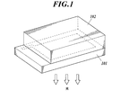
- FIG. 1 shows a schematic diagram of an organic EL element.
- the organic EL element 101 is covered with a glass cover 102.
- the sealing operation with the glass cover 102 was performed in a glove box (in an atmosphere of high-purity nitrogen gas having a purity of 99.999% or more) in a nitrogen atmosphere without bringing the organic EL element 101 into contact with the atmosphere.
- FIG. 2 shows a cross-sectional view of the organic EL element.
- an organic EL layer 106 and a cathode 105 are laminated and formed on a glass substrate 107 with a transparent electrode.
- the glass cover 102 is filled with nitrogen gas 108 and a water catching agent 109 is provided.
- Organic EL element 102 was prepared in the same manner as in the preparation of organic EL element 101 except that the film thickness of the intermediate metal layer was changed to 1 nm.
- Organic EL Element 103 In the production of the organic EL element 101, “organic EL element” was prepared in the same manner except that LiF was formed to a thickness of 1 nm between the layer made of the compound E-1 and the intermediate metal layer. 103 ".
- organic EL element 104 In the preparation of the organic EL element 102, the “organic EL element was formed in the same manner except that LiF was formed to a thickness of 1 nm between the layer made of the compound E-1 and the intermediate metal layer. 104 "was produced.
- Organic EL element 105 was prepared in the same manner as in the preparation of the organic EL element 101 except that the material for forming the intermediate metal layer was changed to Ag.
- Organic EL element 106 was produced in the same manner as in the production of the organic EL element 102 except that the material for forming the intermediate metal layer was changed to Ag.
- Organic EL Element 107 was produced in the same manner as in the production of the organic EL element 102 except that the material for forming the intermediate metal layer was changed to Li.
- Organic EL element 108 was produced in the same manner as in the production of the organic EL element 101, except that the material for forming the intermediate metal layer was changed to Ca.
- Organic EL element 110 was prepared in the same manner as in the preparation of the organic EL element 107, except that the thickness of the intermediate metal layer was 2.5 nm.
- Organic EL element 111 was prepared in the same manner as in the preparation of organic EL element 107, except that the thickness of the intermediate metal layer was 1.5 nm.
- Organic EL element 112 was prepared in the same manner as in the preparation of organic EL element 107, except that the thickness of the intermediate metal layer was 1 nm.
- Organic EL element 113 was produced in the same manner as in the production of organic EL element 107, except that the thickness of the intermediate metal layer was 0.7 nm.
- Organic EL Element 114 “Organic EL element 114” was prepared in the same manner as in the preparation of the organic EL element 108 except that the film thickness of the intermediate metal layer was 1 nm.
- Organic EL element 115 “Organic EL element 115” was produced in the same manner as in the production of the organic EL element 102 except that the material for forming the intermediate metal layer was changed to Cs.
- Organic EL element 116 was prepared in the same manner as in the preparation of organic EL element 102, except that the material for forming the intermediate metal layer was changed to K.
- the organic EL elements 109 to 116 of the present invention have improved emission quantum efficiency and lower voltage than the organic EL elements 101 to 108 of the comparative example. It can be seen that it can be driven. From the above, it can be seen that the intermediate metal layer is made of a metal having a work function of 3.0 eV or less and having a film thickness of 0.6 to 5 nm is useful for improving the light emission efficiency and driving at a low voltage.
- organic EL element 201 As an anode, ITO (indium tin oxide) was formed on a glass substrate having a thickness of 150 nm on a glass substrate of 30 mm ⁇ 30 mm and a thickness of 0.7 mm. A transparent support substrate with an ITO transparent electrode is ultrasonically cleaned with isopropyl alcohol, dried with dry nitrogen gas, UV ozone cleaned for 5 minutes, and then fixed to a substrate holder of a commercially available vacuum deposition apparatus. did.
- ITO indium tin oxide
- Each of the vapor deposition crucibles in the vacuum vapor deposition apparatus was filled with the constituent material of each layer in an optimum amount for device fabrication.
- the evaporation crucible used was made of a resistance heating material made of molybdenum or tungsten.
- lithium was evaporated to a thickness of 6 nm to form an intermediate metal layer.
- Compound M-4 was deposited at a deposition rate of 0.1 nm / second to form a 15 nm thick layer.
- Compound M-2 was deposited at a deposition rate of 0.1 nm / second to form a 50 nm thick layer.
- compounds GD-1, RD-1 and compound H-2 were co-deposited at a deposition rate of 0.1 nm / second so that the concentration of compound GD-1 was 17% and RD-1 was 0.8%.
- a phosphorescent light emitting layer having a film thickness of 30 nm and exhibiting yellow was formed.
- Compound E-1 was deposited at a deposition rate of 0.1 nm / second to form a layer having a thickness of 30 nm.
- aluminum 110 nm was vapor-deposited to form a cathode.
- organic EL elements 202 to 207 In production of organic EL element 201, the thickness of the intermediate metal layer was 4.5 nm, 2.5 nm, 1.5 nm, 1 nm, 0.7 nm, and 0.3 nm, respectively. “Organic EL elements 202 to 207” were produced in the same manner except for the above.
- organic EL element 208 In the production of the organic EL element 201, the organic metal element 201 was formed in the same manner except that the Li film thickness of the intermediate metal layer was 1 nm, and Li was formed to a thickness of 1 nm instead of LiF. An EL element 208 ”was produced.
- the layer configuration of the laminate and the constituent materials of each layer, and other light emission adjacent to the intermediate metal layer side of the laminate are the same except for the light emitting layer. More specifically, the layer configuration from the layer composed of the compound M-4 constituting the light emitting unit to the intermediate metal layer composed of lithium and its constituent materials, and the compound M-4 adjacent to the cathode side of the intermediate metal layer.
- the layer configuration from the layer configured by the above to the layer configured by lithium adjacent to the cathode and the constituent materials thereof are the same except for the light emitting layer.
- the organic EL devices 201 to 208 emitted white light having a correlated color temperature of 3500 to 4000 K at a luminance of 2000 cd / m 2 .
- the organic EL elements 201 to 208 are stored (left) in an environment of 75 ° C. for 500 hours, and when driven at 2.5 mA / cm 2 , the drive voltage and front luminance before and after storage are measured at room temperature ( 25 ° C.), and the fluctuation range was determined as an index of long-term storage stability.
- the front luminance was measured using a spectral radiance meter CS-2000 (manufactured by Konica Minolta Sensing) in the same manner as in Example 1. The evaluation results are shown in Table 2. Note that the fluctuation range of the driving voltage and front luminance of each organic EL element is shown as a relative value with the fluctuation width of the organic EL element 201 being 100.
- the organic EL elements 202 to 206, 208 having the thickness of the intermediate metal layer of the present invention are either initial or long-term storage compared to the organic EL elements 201, 207 of the comparative example. It can also be seen that the fluctuation of the driving voltage is small and the luminance fluctuation during long-term storage is small and good. Specifically, the organic EL element 201 of the comparative example having a thick intermediate metal layer with a thickness of 6 nm has a remarkably large luminance fluctuation especially in long-term storage as compared with the organic EL element of the present invention.
- the comparative organic EL element 207 having a thin intermediate metal layer thickness of 0.3 nm is not significantly inferior to the organic EL element of the present invention in terms of luminance fluctuation during long-term storage.
- the drive voltage fluctuation in the initial stage is remarkably large, and the stability performance is greatly inferior. It can be seen that the storage stability is remarkably improved by setting the thickness of the intermediate metal layer within the range of the present invention.
- the organic EL element 208 with the same structure except for the light emitting layer shows good performance, and the layer structure excluding the light emitting layer of each light emitting unit and the material of each layer are the same, and the simplified production advantages It can be seen that you can enjoy.
- a substrate formed by forming a film of ITO (indium tin oxide) with a thickness of 150 nm on a glass substrate of 30 mm ⁇ 30 mm and a thickness of 0.7 mm was ultrasonically cleaned with isopropyl alcohol and dried with dry nitrogen gas, After performing UV ozone cleaning for 5 minutes, this substrate was fixed to a substrate holder of a commercially available vacuum deposition apparatus.
- Each of the deposition crucibles in the vacuum deposition apparatus was filled with an optimum amount of the film forming material for sample preparation.
- the evaporation crucible used was made of a resistance heating material made of molybdenum or tungsten.
- Compound E-1 was deposited at a deposition rate of 0.1 nm / second to form a layer with a thickness of 30 nm. Subsequently, lithium was vapor-deposited to a desired film thickness, and the non-light-emitting surface of the element was covered with a glass case in the same manner as the organic EL element 101 to prepare a sample.
- the glass case When observing the film surface with an electron microscope, the glass case was peeled from the substrate in a nitrogen gas atmosphere immediately before setting the film-forming sample in the electron microscope to expose the film surface.
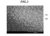
- FIG. 3 is an SEM image observed from above the sample film with a lithium film thickness of 1 nm. Spotted and striped patterns are observed, and lithium is formed on the bright portions 110. That is, the 1 nm-thick intermediate metal layer film of the present invention includes a region where lithium is formed (bright portion 110), a region where lithium is not formed, or a region where the amount of adhesion is small (dark portion 120). It can be seen that it has a fine structure consisting of
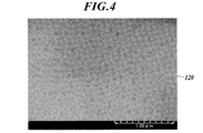
- FIG. 4 is an SEM image observed from above the sample film having a lithium film thickness of 2.5 nm. Although it has a dot-like dark portion 120 and the film is not yet a completely flat surface, the degree of non-flatness is significantly smaller than the 1 nm thick intermediate metal layer shown in FIG.
- Example 2 when the thickness of the intermediate metal layer is 1 nm, the storage stability is better than that of 2.5 nm, and the thickness of the intermediate metal layer correlates with the flatness of the film surface. I understand. When the thickness of the intermediate metal layer exceeded 3 nm, such a bright and dark pattern was not observed, indicating that the intermediate metal layer film surface was flat.
- organic EL element 401 In the preparation of the organic EL element 205, a layer made of the compound E-1 was formed adjacent to the fluorescent light emitting layer, and then KF was deposited to a thickness of 1.5 nm and a deposition rate of 0.01 nm.
- the “organic EL element 401” was prepared in the same manner except that the film was formed at a rate of / sec and an intermediate metal layer made of lithium was formed.
- organic EL element 402 In the preparation of the organic EL element 205, the volume ratio of the compound E-1 and KF is 85:15 by changing to the layer made of the compound E-1 adjacent to the fluorescent light emitting layer. Thus, “organic EL element 402” was produced in the same manner except that the film was formed at a deposition rate of 0.1 nm / second.
- organic EL element 403 In production of the organic EL element 205, the volume ratio of the compound E-1 and LiF is 80:20 instead of the layer made of the compound E-1 adjacent to the fluorescent light emitting layer. Thus, “organic EL element 403” was produced in the same manner except that the film was formed at a deposition rate of 0.1 nm / second.
- the organic EL element 205 in which the layer adjacent to the anode side of the intermediate metal layer is a layer formed by forming a single organic compound is an organic EL element in which the adjacent layer is an inorganic compound. It can be seen that the long-term storage stability is particularly excellent as compared with the element 401 or the organic EL elements 402 and 403 in which the adjacent layer is a mixed layer of an organic compound and an inorganic compound.
- organic EL element 501 In the preparation of organic EL element 205, a layer made of compound E-2 was formed in the same manner except that a layer made of compound E-1 was formed adjacent to the fluorescent light emitting layer. An “organic EL element 501” was produced.
- organic EL element 502 Preparation of organic EL element 502
- KF was formed to a film thickness of 1.5 nm at a deposition rate of 0.01 nm / second
- An “organic EL element 502” was produced in the same manner except that an intermediate metal layer made of lithium was formed.
- the adjacent layer is formed by forming a single organic compound. It can be seen that the organic EL element 501 which is the layer formed is superior in long-term storage stability compared to the organic EL element 502 whose adjacent layer is an inorganic compound.
- organic EL element 601 As an anode, ITO (Indium Tin Oxide) is formed to a thickness of 150 nm on a glass substrate having a size of 30 mm ⁇ 30 mm and a thickness of 0.7 mm. A transparent support substrate with an ITO transparent electrode is ultrasonically cleaned with isopropyl alcohol, dried with dry nitrogen gas, UV ozone cleaned for 5 minutes, and then fixed to a substrate holder of a commercially available vacuum deposition apparatus. did.
- ITO Indium Tin Oxide
- Each of the vapor deposition crucibles in the vacuum vapor deposition apparatus was filled with the constituent material of each layer in an optimum amount for device fabrication.
- the evaporation crucible used was made of a resistance heating material made of molybdenum or tungsten.
- Compound BD-2 and Compound H-2 are co-evaporated at a deposition rate of 0.1 nm / second so that the concentration of Compound BD-2 is 12%, and a phosphorescent light-emitting layer exhibiting blue light emission with a film thickness of 20 nm Formed.
- Compound F-1 was deposited at a deposition rate of 0.1 nm / second to form a layer with a thickness of 5 nm.
- Compound E-1 was deposited at a deposition rate of 0.1 nm / second to obtain a thickness of 30 nm. Layers were formed.
- lithium was evaporated to a thickness of 6 nm to form an intermediate metal layer.
- the film formation from the compound M-4 to the compound E-2 was repeated once more, and lithium was further formed with a film thickness of 1 nm, and then aluminum 110 nm was deposited to form a cathode.
- Organic EL element 602 was produced in the same manner as in the production of organic EL element 601, except that the thickness of the intermediate metal layer was 1 nm.
- Organic EL element 603 was prepared in the same manner as in the preparation of organic EL element 601, except that the thickness of the intermediate metal layer was 0.4 nm.
- Each of the organic EL elements exhibited white light emission with a correlated color temperature of about 2800 K at a front luminance of 1000 cd / m 2 .
- Example 2 the driving voltage, external extraction light emission quantum efficiency and storage stability were evaluated, and the same results as in Example 2 were obtained in relation to the film thickness of the intermediate metal layer and these various performances.
- the effect of the present invention was also confirmed in an organic EL element using phosphorescent light emitting materials for all light emitting materials.
- organic EL element 701 As an anode, ITO (Indium Tin Oxide) was formed to a thickness of 150 nm on a glass substrate having a thickness of 30 mm ⁇ 30 mm and a thickness of 0.7 mm. A transparent support substrate with an ITO transparent electrode is ultrasonically cleaned with isopropyl alcohol, dried with dry nitrogen gas, UV ozone cleaned for 5 minutes, and then fixed to a substrate holder of a commercially available vacuum deposition apparatus. did.
- ITO Indium Tin Oxide
- Each of the vapor deposition crucibles in the vacuum vapor deposition apparatus was filled with the constituent material of each layer in an optimum amount for device fabrication.
- the evaporation crucible used was made of a resistance heating material made of molybdenum or tungsten.
- lithium was evaporated to a thickness of 6 nm to form a first intermediate metal layer.
- a 15 nm-thick layer composed of the compound M-4 and a 40 nm-thick layer composed of the compound M-2 were formed in the same manner as described above. Thereafter, compounds GD-1, RD-1 and compound H-2 were co-deposited at a deposition rate of 0.1 nm / second so that the concentration of compound GD-1 was 8% and RD-1 was 1.5%. A phosphorescent light emitting layer exhibiting a red color with a thickness of 25 nm was formed. Next, Compound E-1 was deposited at a deposition rate of 0.1 nm / second to form a 25 nm thick layer.
- lithium was evaporated to a thickness of 6 nm to provide a second intermediate metal layer.
- a 15 nm-thick layer composed of the compound M-4 and a 40 nm-thick layer composed of the compound M-2 were formed in the same manner as described above.
- Compound BD-1 and Compound H-1 are co-evaporated at a deposition rate of 0.1 nm / second so that Compound BD-1 has a concentration of 5%, and a fluorescent light-emitting layer exhibiting blue light emission with a film thickness of 25 nm is formed.
- Compound E-1 was deposited at a deposition rate of 0.1 nm / second to form a layer having a thickness of 35 nm. Further, after forming lithium with a film thickness of 1 nm, aluminum was deposited with a thickness of 110 nm to form a cathode.
- the organic EL element 701 is an element having two intermediate metal layers.
- Organic EL element 702 was produced in the same manner as in the production of organic EL element 701, except that the thickness of the first and second intermediate metal layers was 1 nm.
- Organic EL element 703 was produced in the same manner as in the production of organic EL element 701, except that the thickness of the first and second intermediate metal layers was 0.4 nm.
- Example 2 the driving voltage, external extraction light emission quantum efficiency and storage stability were evaluated, and the same results as in Example 2 were obtained in relation to the film thickness of the intermediate metal layer and these various performances. The effect of the present invention was also confirmed in an organic EL device having two or more intermediate metal layers.
- the present invention provides an organic EL element having a laminated structure of a plurality of light emitting units, which is excellent in low driving voltage, high light emission efficiency, storage stability, and improved productivity, and further provides an organic EL element exhibiting white light emission. In particular, it can be suitably used.
Landscapes
- Physics & Mathematics (AREA)
- Optics & Photonics (AREA)
- Electroluminescent Light Sources (AREA)
Description
このような構成からなる有機EL素子は、一般的に発光電流効率と駆動寿命とがトレードオフの関係になることが知られている。そのため、このトレードオフの関係を改善するべく、有機材料、有機層構成、素子駆動方法等、様々な視点から検討が加えられてきた。
「特許文献2」には、少なくとも2層からなる中間導電層について開示されており、具体的には厚さ8nmのMg-Ag合金膜と厚さ10nmのIn-Zn-O導電膜との積層構造等が開示されている。
「特許文献4」および「特許文献5」にも、同様にアクセプターおよびドナーをドープした有機層を積層することによる中間層が開示されている。
具体的には、「特許文献6」の実施例において、Al(仕事関数約4.3eV)を用いた膜厚6nmの構成が開示されているが、Al層のみでは駆動電圧が高いため、金属層の陽極側に隣接して電子注入性層が必要となる。実際に電子注入性層材料としてLiFを用いた構成が開示されている。結果として、無機層を1層挿入する必要があり、生産面での負荷が増大するとともに、実質的にはLiF/Alの2層構成にて中間層としての機能を発現しているとも考えられる。また、該金属層の膜厚が6nmと厚いため、金属層の吸収による効率低下以外にも、保存安定性、駆動安定性に課題があることがわかってきた。
「特許文献7」の実施例には、金属層(中間ユニット)として膜厚0.3nmのLi層を用いた構成が開示されているが、金属層膜厚が0.3nm程度と薄いため、やはり有機EL素子の安定性能、特に駆動初期あるいは素子作製後比較的短期における性能変動が大きく課題があることがわかってきた。
前記中間金属層が、仕事関数3.0eV以下の金属から構成され、かつ、膜厚が0.6~5nmであることを特徴とする有機エレクトロルミネッセンス素子。
前記積層体の層構成および各層の構成材料と、前記積層体の前記中間金属層側に隣接する他の発光ユニットまたは他の積層体の層構成および各層の構成材料とが、発光層を除いて同一であることを特徴とする前記1に記載の有機エレクトロルミネッセンス素子。
本発明の有機EL素子は、照明装置に好適に具備され得る。
本発明の有機EL素子の層構成の好ましい具体例を以下に示すが、本発明はこれらに限定されない。
(II)陽極/第1発光ユニット/第1中間金属層/第2発光ユニット/第2中間金属層/第3発光ユニット/陰極
(III)陽極/第1発光ユニット/第1中間金属層/第2発光ユニット/第2中間金属層/第3発光ユニット/第3中間金属層/第4発光ユニット/陰極
(I-2)陽極/青色発光ユニット/中間金属層/緑・赤色発光ユニット/陰極
(I-3)陽極/緑・赤色発光ユニット/中間金属層/青色発光ユニット/陰極
(II-1)陽極/青色発光ユニット/第1中間金属層/青色発光ユニット/第2中間金属層/緑・赤色発光ユニット/陰極
(II-2)陽極/青色発光ユニット/第1中間金属層/緑色発光ユニット/第2中間金属層/赤色発光ユニット/陰極
(II-3)陽極/緑色発光ユニット/第1中間金属層/赤色発光ユニット/第2中間金属層/青色発光ユニット/陰極
(ii)正孔注入輸送層/第1発光層/第2発光層/電子注入輸送層
(iii)正孔注入輸送層/第1発光層/中間層/第2発光層/電子注入輸送層
(iv)正孔注入輸送層/発光層/正孔阻止層/電子注入輸送層
(v)正孔注入輸送層/電子阻止層/発光層/正孔阻止層/電子注入輸送層
(vi)正孔注入層/正孔輸送層/発光層/電子輸送層/電子注入層
(vii)正孔注入層/正孔輸送層/発光層/正孔阻止層/電子輸送層/電子注入層
(viii)正孔注入層/正孔輸送層/電子阻止層/発光層/正孔阻止層/電子輸送層/電子注入層
また、発光層に含有される発光ドーパントは、発光層の膜厚方向に対し、均一な濃度で含有されていてもよく、また濃度分布を有していてもよい。
上記理由より、白色発光ユニットを積層する場合には、発光層を含む全層の構成、材料が同じであることがなお好ましい。
なお、「補色」の関係とは、混合すると無彩色になる色同士の関係をいう。つまり、補色の関係にある色を発光する物質の発光を混合すると、白色発光を得ることができる。
また、青、緑、赤の発光材料を1つの発光層中に混在させ白色発光を呈する発光層として、発光ユニットに設けることもできる。
本発明においては、光色の黒体輻射軌跡からの偏差Duvが、相関色温度が2500~7500Kの範囲内において、-20~+20の範囲に含まれる光を白色光と呼ぶものとする。Duv(=1000duv)の定義は、JIS Z 8725:1999「光源の分布温度および色温度・相関色温度測定方法」による。
本発明にかかる中間金属層は、2つの発光ユニット間に配置され、形成されている。
中間金属層は、その一部微細領域にほとんど金属材料が製膜されていない状態、いわゆるピンホールが形成されていたり、面内方向において網状に形成されていてもよい。あるいは、中間金属層形成部分が島状(斑状)に形成されていてもよい。
中間金属層に用いられる材料としては、カルシウム(仕事関数2.87eV、融点1112.2K)、リチウム(同2.9eV、同453.7K)、ナトリウム(同2.75eV、同371K)、カリウム(同2.3eV、同336.9K)、セシウム(同2.14eV、同301.6K)、ルビジウム(同2.16eV、同312.1K)、バリウム(同2.7eV、同998.2K)、ストロンチウム(同2.59eV、同1042.2K)が挙げられるが、中でも常圧での融点が400K以上であり、有機EL素子の高温環境下での性能を損うおそれの小さいリチウム、カルシウム、バリウム、ストロンチウムが好ましい。
一方、本発明者らの検討によれば、中間金属層の膜厚が0.6nm未満の場合には、有機EL素子の性能安定性、特にその素子作製後、比較的初期段階における性能変動が大きいことが判明した。これら初期の安定性が劣化する原因は定かではないが、膜厚が過剰に薄く、数オングストロームの膜厚の金属膜、またはクラスター径からなる金属塊からなる場合には、その物理的、化学的安定性が金属バルクの状態とは大きく異なり、隣接層材料との酸化還元反応を含む化学的反応、あるいは熱、素子の駆動に伴う電荷との相互作用等により、金属膜または金属塊の状態が変化し、さらには、その一部の金属原子またはイオンの隣接層への拡散等の現象が発生する可能性が高くなることが想定される。このように、製膜直後の状態からの一定の準安定状態への移行に伴い性能変化が生じるものと考えられる。
一方、「特許文献7」の実施例には、金属層として膜厚0.3nmのLi層を用いた構成が開示されているが、上記記述および後述の実施例に示されるように、中間金属層の膜厚が0.3nm程度と薄い場合には、有機EL素子の駆動初期あるいは素子作製後比較的短期における性能変動が大きいことが判明した。
このような機能を有する層として、電荷輸送性を高めるため、たとえば、電荷輸送性有機材料と、該有機材料を酸化もしくは還元できる、あるいは該有機材料と電荷移動錯体を形成しうるような無機材料または有機金属錯体等とをドーピングした混合層を形成することが知られている。
以下、発光層に含まれるホスト化合物およびドーパント化合物について説明する。
本発明に用いられるリン光ホスト化合物としては、構造的には特に制限はないが、代表的にはカルバゾール誘導体、トリアリールアミン誘導体、芳香族ボラン誘導体、含窒素複素環化合物、チオフェン誘導体、フラン誘導体、オリゴアリーレン化合物等の基本骨格を有するもの、または、カルボリン誘導体やジアザカルバゾール誘導体(ここで、ジアザカルバゾール誘導体とは、カルボリン誘導体のカルボリン環を構成する炭化水素環の少なくとも一つの炭素原子が窒素原子で置換されているものを表す。)等が挙げられる。
リン光ホスト化合物は、単独で用いてもよく、または複数種併用して用いてもよい。

これらの置換基は、上記の置換基によってさらに置換されていてもよい。また、これらの置換基は複数が互いに結合して環を形成していてもよい。
一般式(a)において、好ましい「X」はNR′またはOであり、R′としては芳香族炭化水素基、芳香族複素環基が特に好ましい。
また、一般式(a)において、nは0~8の整数を表すが、0~2の整数であることが好ましく、特に「X」がO,Sである場合には1または2であることが好ましい。
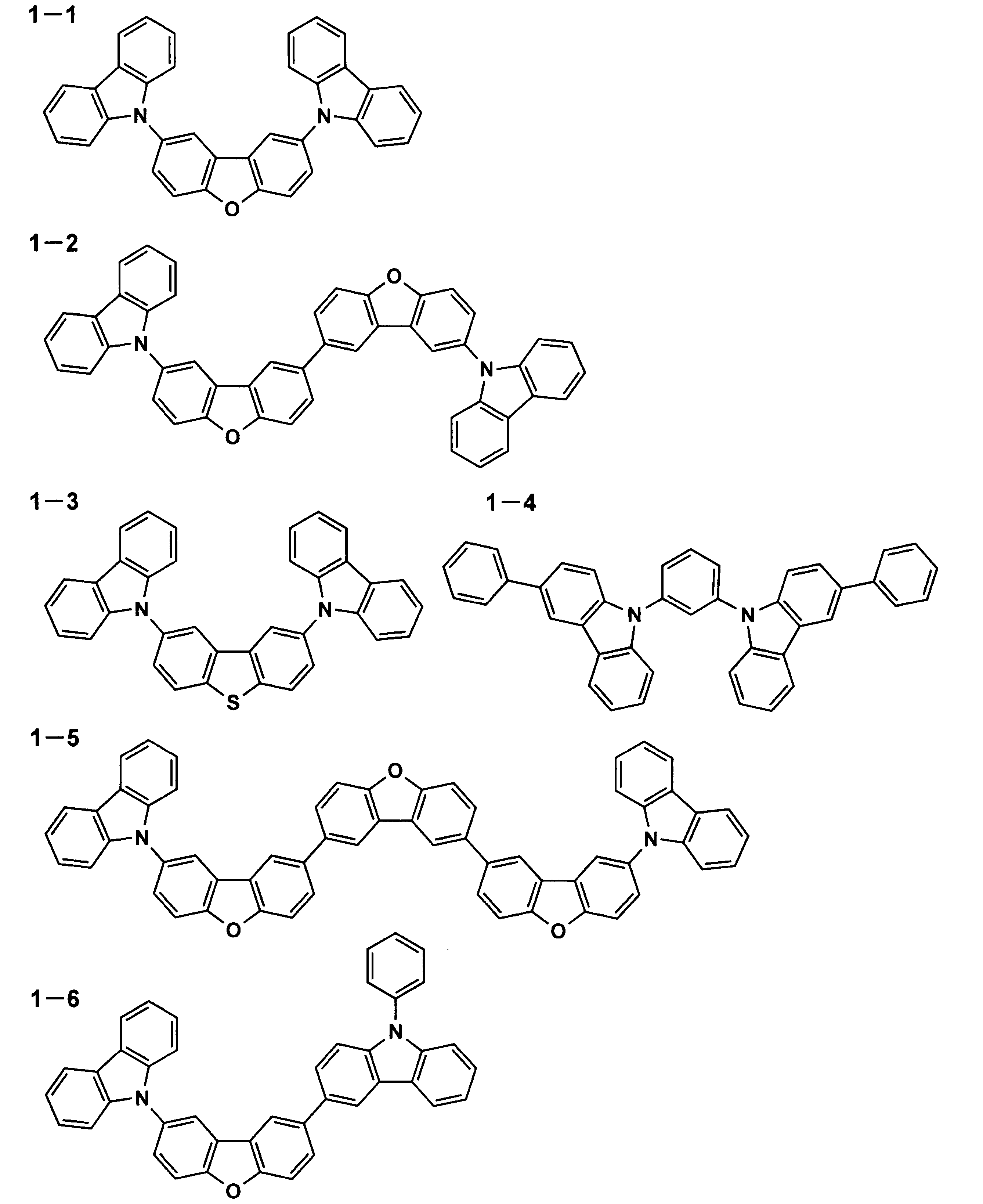

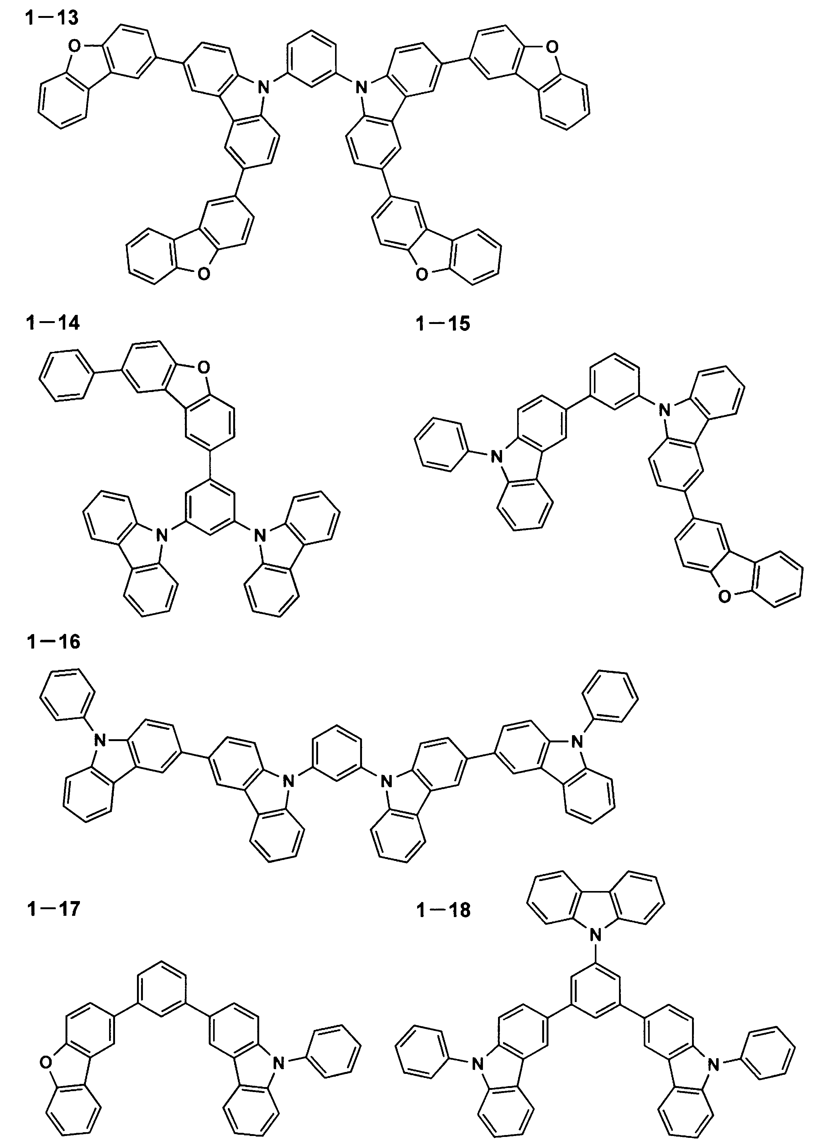
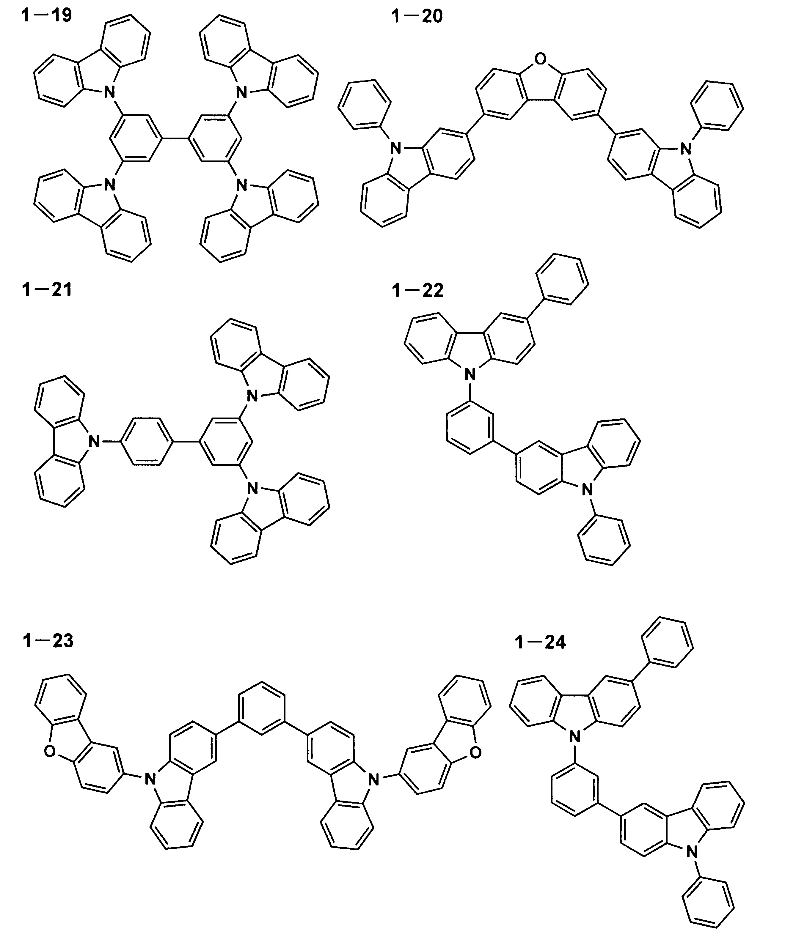

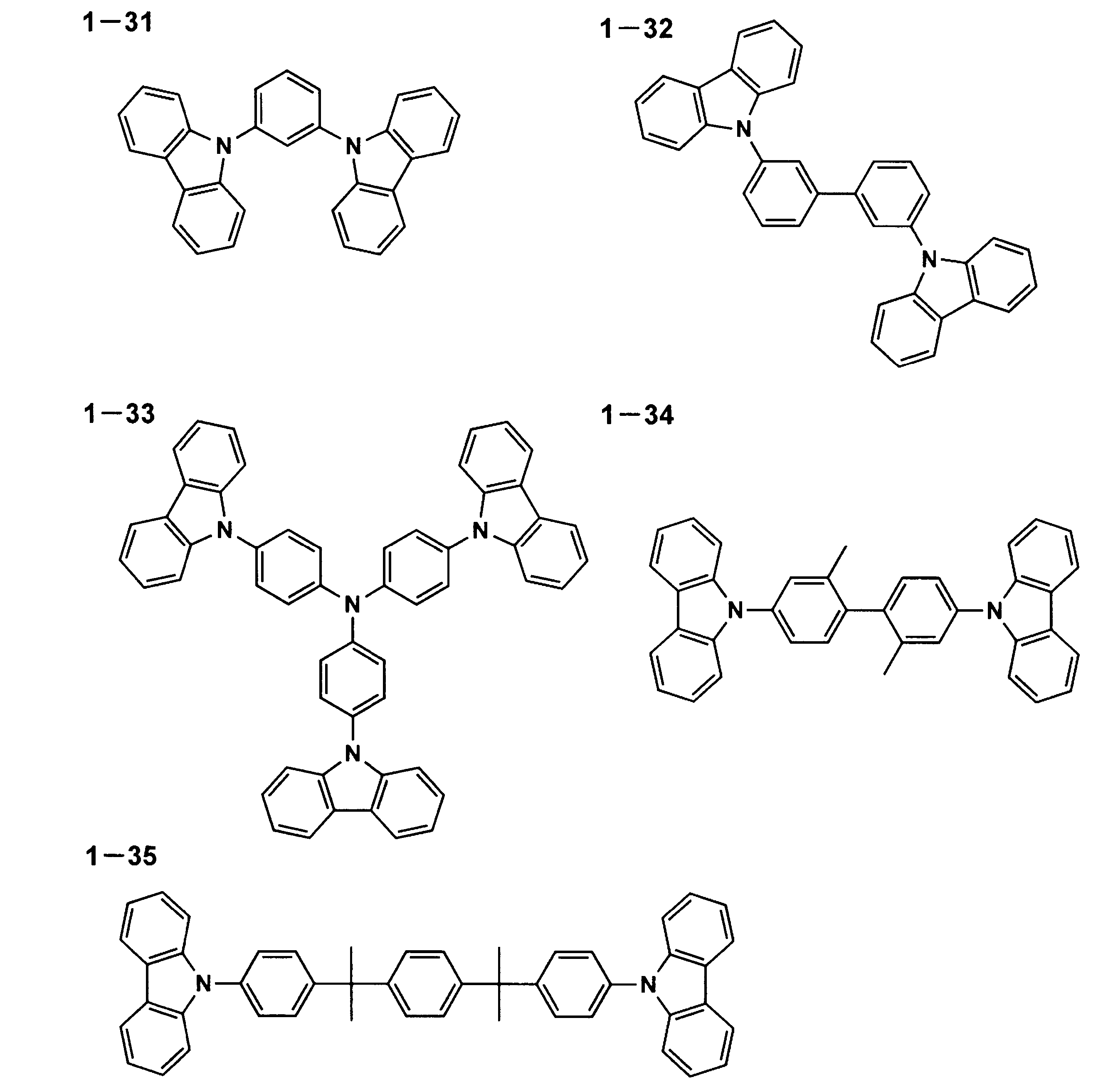
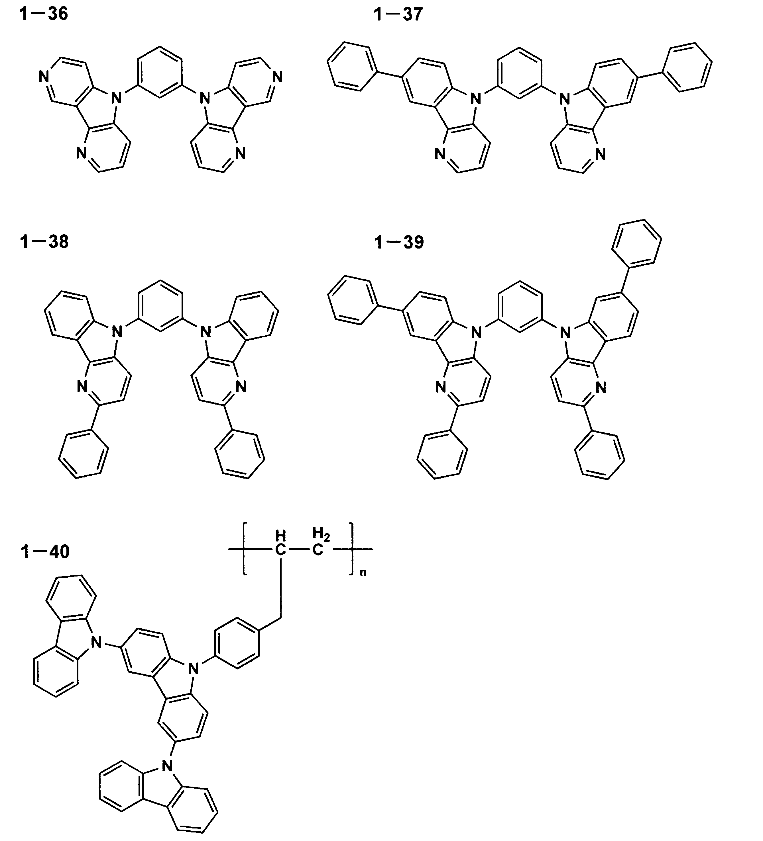
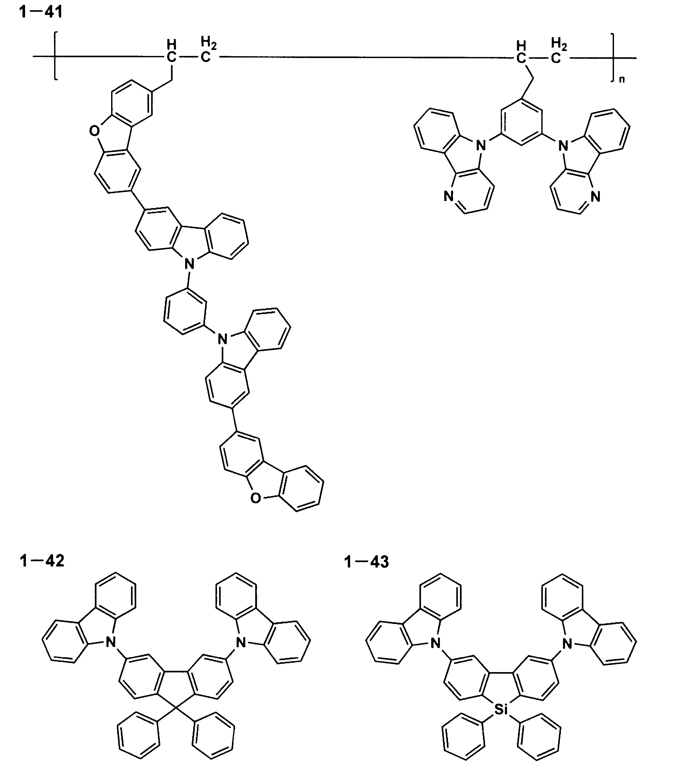
ここで、ガラス転移点(Tg)とは、DSC(Differential Scanning Colorimetry:示差走査熱量法)を用いて、JIS K 7121に準拠した方法により求められる値である。
また、リン光ホスト化合物は、その最低励起3重項エネルギー(T1)が、2.7eVより大きいことがより高い発光効率を得られることから好ましい。
本発明でいう最低励起3重項エネルギーとは、ホスト化合物を溶媒に溶解し、液体窒素温度において観測したリン光発光スペクトルの最低振動バンド間遷移に対応する発光バンドのピークエネルギーをいう。
本発明に用いることができるリン光発光ドーパントは、公知のものの中から選ぶことができる。たとえば、元素の周期表で8族~10族の金属を含有する錯体系化合物、好ましくはイリジウム化合物、オスミウム化合物、もしくは白金化合物(白金錯体系化合物)、または希土類錯体から選ぶことができる。中でも最も好ましいのはイリジウム化合物である。
本発明の白色発光を呈する有機EL素子を作製する場合には、少なくとも緑、黄、赤領域の発光を担う発光体としてはリン光発光材料が好ましい。
また、本発明に青色リン光発光ドーパントを用いる場合には、有機EL素子の発光層に使用される公知のものの中から適宜選択して用いることができるが、下記一般式(A)~(C)から選ばれる少なくとも1つの部分構造を有していることが好ましい。


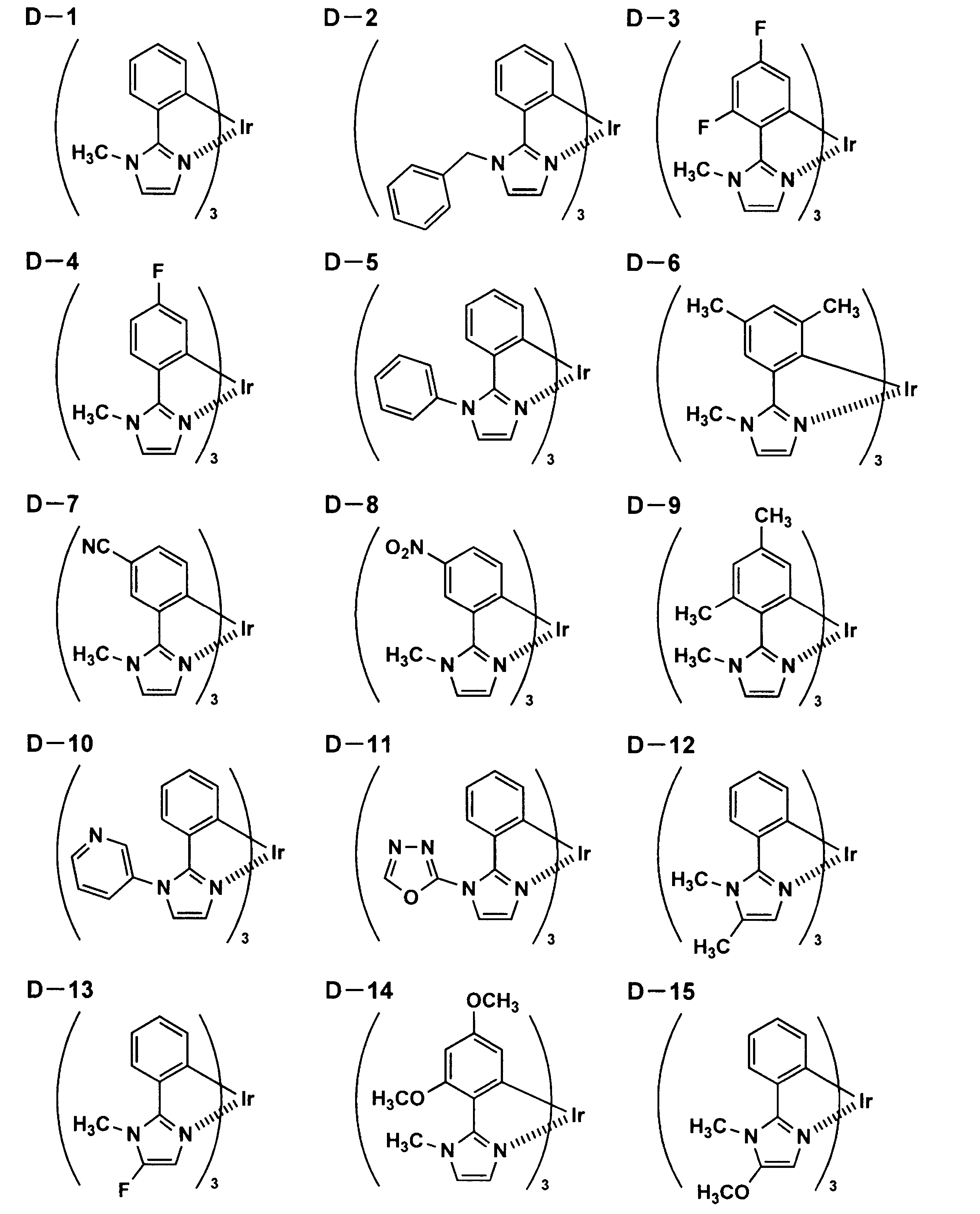


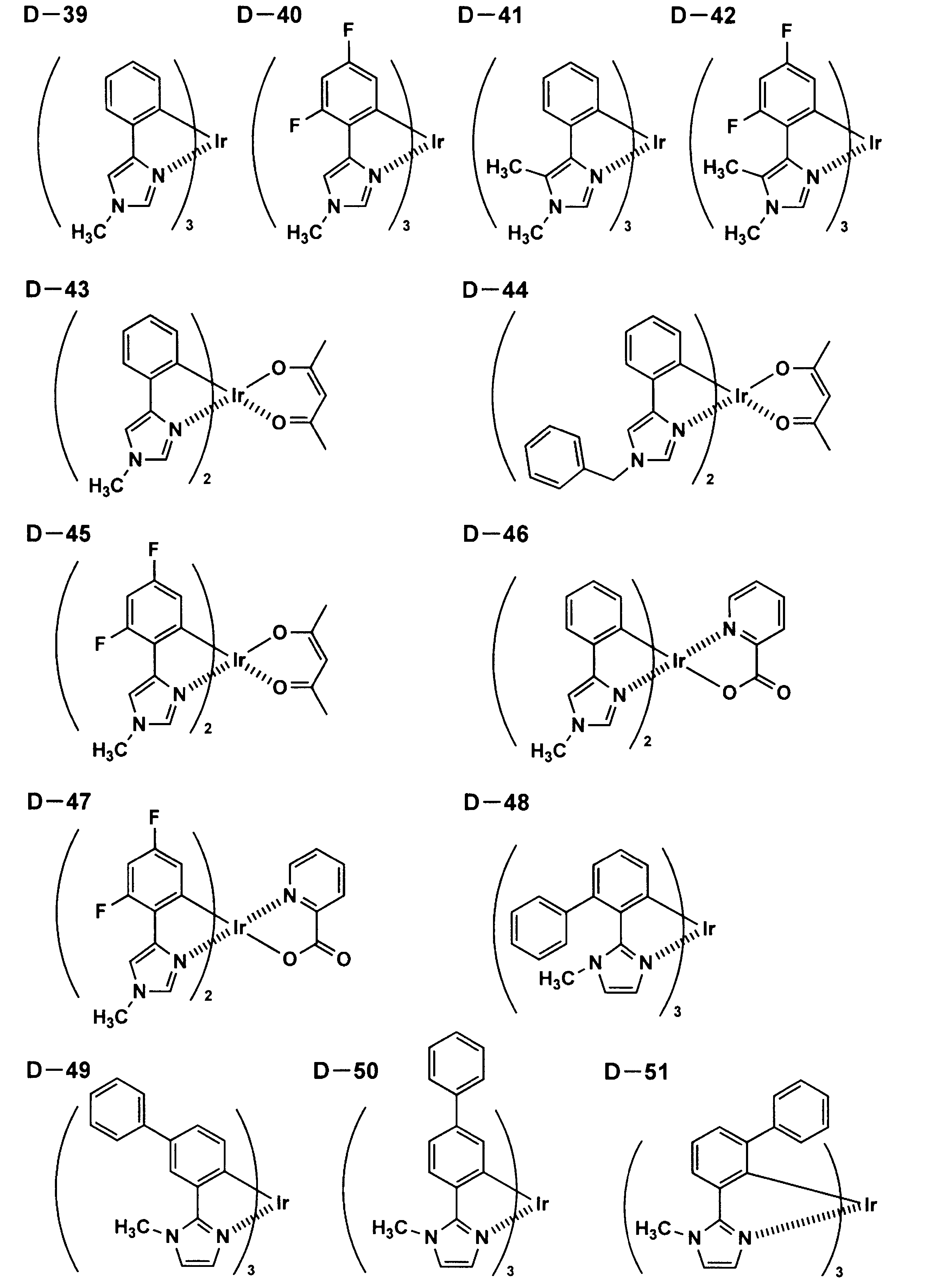
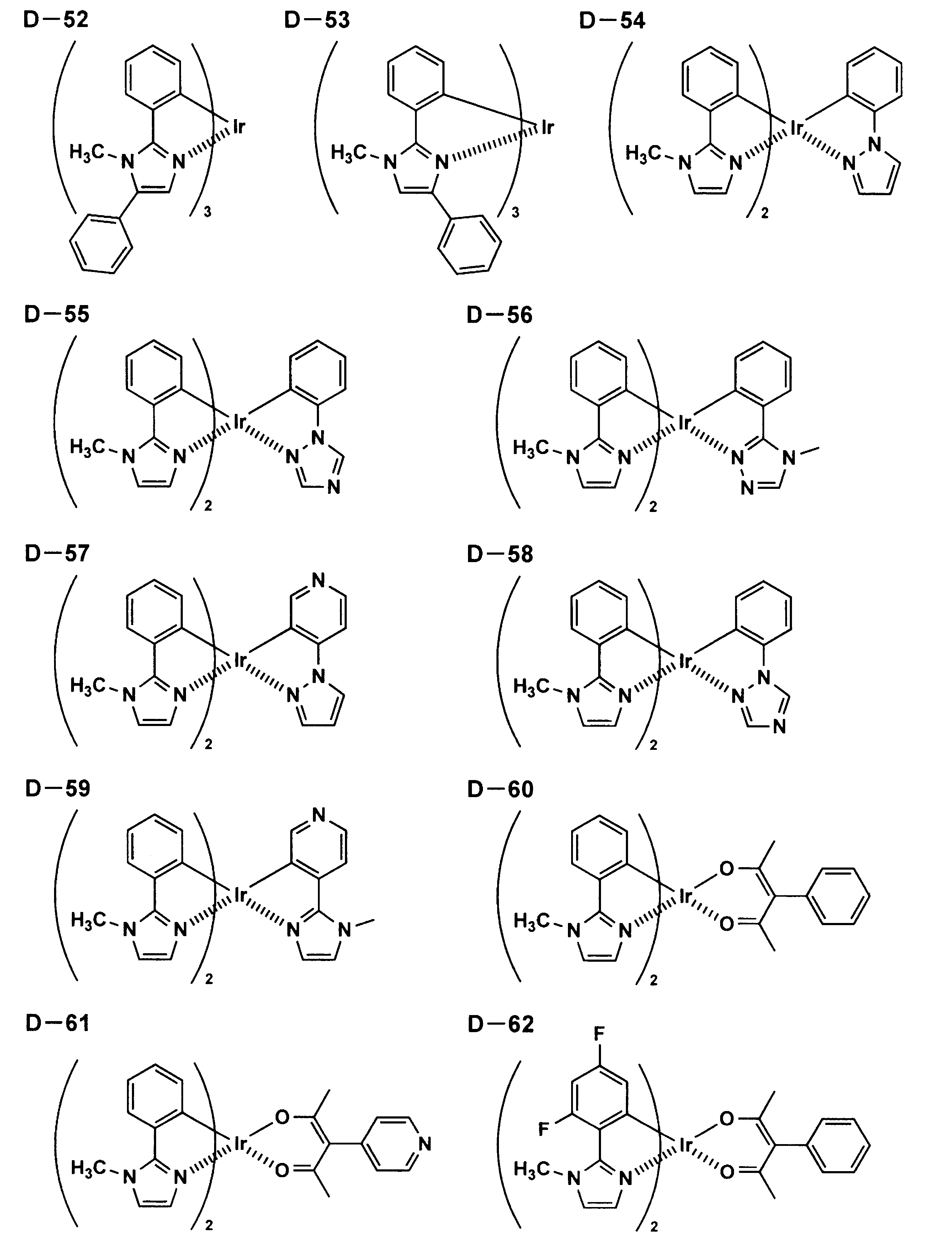
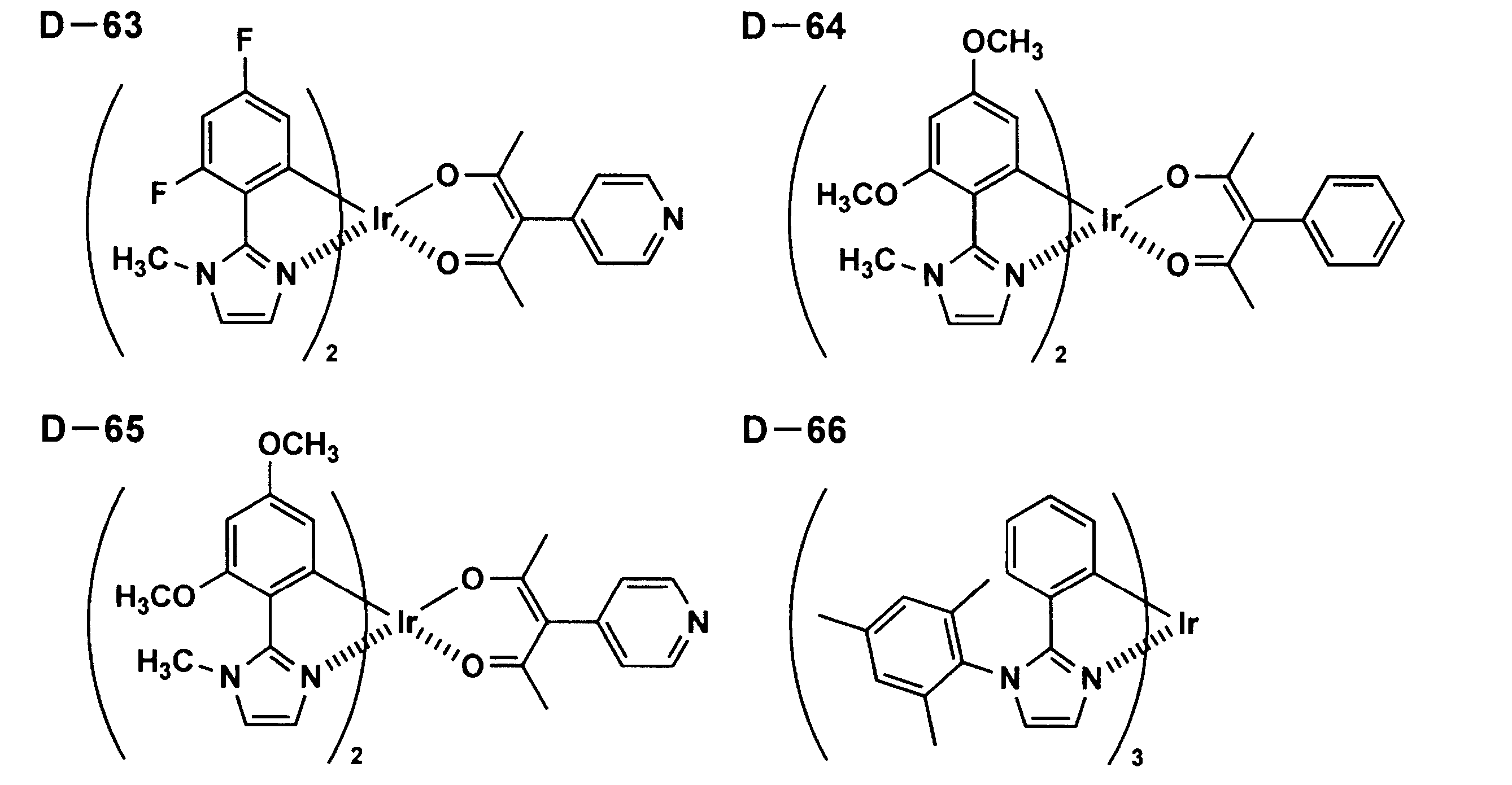

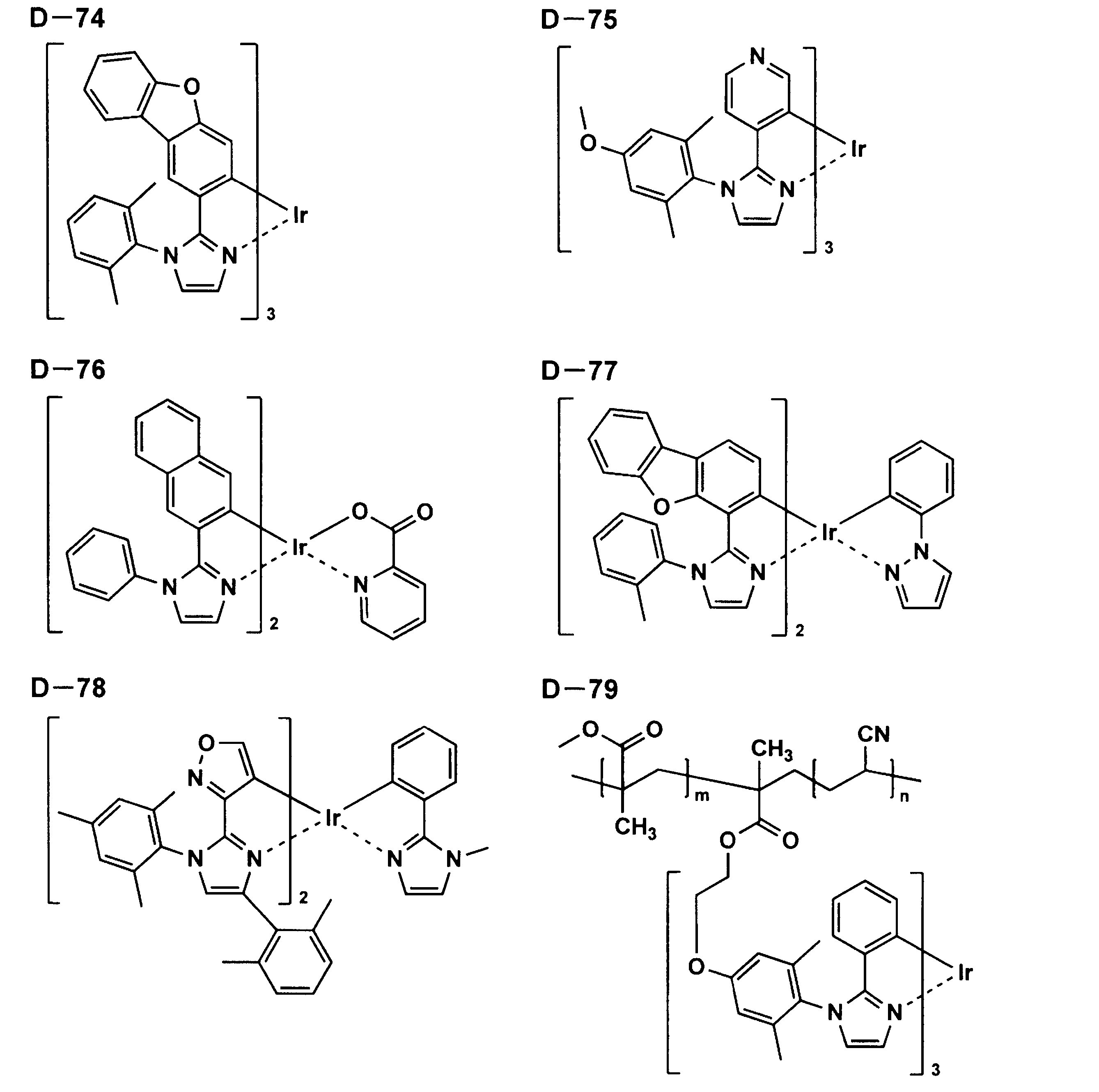


蛍光発光ドーパントとしては、クマリン系色素、ピラン系色素、シアニン系色素、クロコニウム系色素、スクアリウム系色素、オキソベンツアントラセン系色素、フルオレセイン系色素、ローダミン系色素、ピリリウム系色素、ペリレン系色素、スチルベン系色素、ポリチオフェン系色素、または希土類錯体系蛍光体等が挙げられる。
注入層は必要に応じて設けることができ、陽極または中間金属層と発光層または正孔輸送層との間、および陰極または中間金属層と発光層または電子輸送層との間に存在させてもよい。
本発明においては、中間金属層の陽極側に隣接する層としてはアルカリ金属化合物あるいはアルカリ土類化合物からなる層は設けないことが好ましい。
阻止層は、必要に応じて設けられるものである。たとえば、特開平11-204258号公報、同11-204359号公報、および「有機EL素子とその工業化最前線(1998年11月30日エヌ・ティー・エス社発行)」の237頁等に記載されている正孔阻止(ホールブロック)層がある。
本発明の有機EL素子に設ける正孔阻止層は、発光層に隣接して設けられていることが好ましい。
正孔輸送層とは、正孔を輸送する機能を有する正孔輸送材料からなり、広い意味で正孔注入層、電子阻止層も正孔輸送層に含まれる。正孔輸送層は単層または複数層設けることができる。
正孔輸送材料としては上記のものを使用することができるが、さらには、ポルフィリン化合物、芳香族第3級アミン化合物およびスチリルアミン化合物、特に芳香族第3級アミン化合物を用いることが好ましい。
また、特開平4-297076号公報、特開2000-196140号公報、特開2001-102175号公報、J.Appl.Phys.,95,5773(2004)、特開平11-251067号公報、J.Huang et.al.著文献(Applied Physics Letters 80(2002),p.139)、特表2003-519432号公報に記載されているような、いわゆるp型半導体的性質を有するとされる正孔輸送材料を用いることもできる。本発明においては、より高効率の発光素子が得られることから、これらの材料を用いることが好ましい。
電子輸送層とは、電子を輸送する機能を有する材料からなる。電子輸送層は単層または複数層設けることができる。
本発明においては、中間金属層に隣接して電子輸送層を設ける場合には、ピリジン環をその構造の中に包含する化合物であることが好ましい。
電子輸送層の膜厚については特に制限はないが、通常は5nm~5μm程度の範囲内、好ましくは5~200nmの範囲内である。
本発明の有機EL素子に適用する支持基板(以下、基体、基板、基材、支持体等ともいう)としては、ガラス、プラスチック等の種類には特に限定はなく、また、透明であっても不透明であってもよい。支持基板側から光を取り出す場合には、支持基板は透明であることが好ましい。好ましく用いられる透明な支持基板としては、ガラス、石英、透明樹脂フィルムを挙げることができる。特に好ましい支持基板は、有機EL素子にフレキシブル性を与えることが可能な樹脂フィルムである。
本発明の有機EL素子の封止に用いられる封止手段としては、たとえば、封止部材と、電極、支持基板とを接着剤で接着する方法を挙げることができる。
封止部材としては、有機EL素子の表示領域を覆うように配置されていればよく、凹板状でも、平板状でもよい。また、透明性、電気絶縁性は特に限定されない。
素子の機械的強度を高めるために、上記封止用フィルムの外側に保護膜あるいは保護板を設けてもよい。特に、封止が上記封止膜により行われている場合には、その機械的強度は必ずしも高くないため、このような保護膜、保護板を設けることが好ましい。これに使用することができる材料としては、上記封止に用いたのと同様のガラス板、ポリマー板・フィルム、金属板・フィルム等を用いることができるが、軽量かつ薄膜化ということからポリマーフィルムを用いることが好ましい。
有機EL素子における陽極としては、仕事関数の大きい(4eV以上)金属、合金、電気伝導性化合物およびこれらの混合物を電極物質とするものが好ましく用いられる。このような電極物質の具体例としては、Au、Ag、Al等の金属、CuI、インジウムチンオキシド(ITO)、SnO2、ZnO等の導電性透明材料が挙げられる。また、IDIXO(In2O3-ZnO)等非晶質で透明導電膜を作製可能な材料を用いてもよい。
膜厚は材料にもよるが、通常5~1000nmの範囲内、好ましくは5~200nmの範囲内で選ばれる。
一方、陰極としては、金属、合金、電気伝導性化合物およびこれらの混合物を電極物質とするものが用いられる。このような電極物質の具体例としては、ナトリウム、ナトリウム-カリウム合金、マグネシウム、リチウム、マグネシウム/銅混合物、マグネシウム/銀混合物、マグネシウム/アルミニウム混合物、マグネシウム/インジウム混合物、アルミニウム/酸化アルミニウム(Al2O3)混合物、インジウム、リチウム/アルミニウム混合物、希土類金属、銀、アルミニウム等が挙げられる。これらの中で、電子注入性および酸化等に対する耐久性の点から、電子注入性金属とこれより仕事関数の値が大きく安定な金属である第二金属との混合物、たとえば、マグネシウム/銀混合物、マグネシウム/アルミニウム混合物、マグネシウム/インジウム混合物、アルミニウム/酸化アルミニウム(Al2O3)混合物、リチウム/アルミニウム混合物や、アルミニウム、銀等が好適である。
また、陰極に上記材料を1~20nmの範囲内の膜厚で作製した後に、陽極の説明で挙げた導電性透明材料をその上に作製することで、透明または半透明の陰極を作製することができ、これを応用することで陽極と陰極の両方が透過性を有する素子を作製することができる。
本発明の有機EL素子の作製方法の一例として、陽極/第1発光ユニット/中間金属層/第2発光ユニット/陰極からなり、第1発光ユニットが陽極側から正孔注入層/正孔輸送層/発光層/電子輸送層、第2発光ユニットが中間金属層側から正孔注入層/正孔輸送層/発光層/電子輸送層/電子注入層からなる有機EL素子の作製法について説明する。
第1発光ユニットを構成する各層の製膜に際し、層毎に異なる製膜法を適用してもよい。製膜に蒸着法を採用する場合、その蒸着条件は使用する化合物の種類等により異なるが、一般に、それぞれボート加熱温度50~450℃、真空度1×10⁻⁶~1×10⁻²Pa、蒸着速度0.01~50nm/秒、基板温度-50~300℃、膜厚0.1nm~5μm、好ましくは5~200nmの範囲内で適宜選ぶことが望ましい。
有機EL素子は、空気よりも屈折率の高い(屈折率1.6~2.1程度の範囲内)層の内部で発光し、発光層で発生した光のうち15~20%程度の光しか取り出せないことが一般的に言われている。これは、臨界角以上の角度θで界面(透明基板と空気との界面)に入射する光は、全反射を起こし素子外部に取り出すことができないことや、透明電極または発光層と透明基板との間で光が全反射を起こし、光が透明電極または発光層を導波し、結果として、光が素子側面方向に逃げるためである。
本発明は、これらの手段を組み合わせることにより、さらに高輝度あるいは耐久性に優れた素子を得ることができる。
低屈折率層としては、たとえば、エアロゲル、多孔質シリカ、フッ化マグネシウム、フッ素系ポリマーなどが挙げられる。透明基板の屈折率は一般に1.5~1.7程度の範囲内であるので、低屈折率層は、屈折率がおよそ1.5以下であることが好ましく、1.35以下であることがより好ましい。
しかしながら、屈折率分布を二次元的な分布にすることにより、あらゆる方向に進む光が回折され、光の取り出し効率が上がる。
プリズムシートの形状としては、たとえば基材に頂角90度、ピッチ50μmの△状のストライプが形成されたものであってもよいし、頂角が丸みを帯びた形状、ピッチをランダムに変化させた形状、その他の形状であってもよい。
また、有機EL素子からの光放射角を制御するために光拡散板・フィルムを、集光シートと併用してもよい。たとえば、(株)きもと製拡散フィルム(ライトアップ)などを用いることができる。
本発明の有機EL素子を適用した表示装置について説明する。
本発明の有機EL素子は、白色の表示装置に用いられることが好ましい。白色の表示装置の場合は、発光層形成時のみシャドーマスクを設け、一面に蒸着法、キャスト法、スピンコート法、インクジェット法、印刷法、スロット型コータ法等で膜を形成できる。発光層のみパターニングを行う場合、その方法に限定はないが、好ましくは蒸着法、インクジェット法、印刷法である。蒸着法を用いる場合においてはシャドーマスクを用いたパターニングが好ましい。
このようにして得られた多色または白色の表示装置に直流電圧を印加する場合には、陽極を+、陰極を-の極性として電圧2~40V程度の範囲内を印加すると、発光が観測できる。
本発明の有機EL素子を適用した照明装置について説明する。
本発明の有機EL素子は、照明用や露光光源のような一種のランプとして使用してもよいし、画像を投影するタイプのプロジェクション装置や、静止画像や動画像を直接視認するタイプの表示装置(ディスプレイ)として使用してもよい。動画再生用の表示装置として使用する場合の駆動方式は、単純マトリクス(パッシブマトリクス)方式でもアクティブマトリクス方式でもどちらでもよい。
本発明に用いられる白色有機EL素子においては、必要に応じ製膜時にメタルマスクやインクジェットプリンティング法等でパターニングを施してもよい。パターニングする場合は、電極のみをパターニングしてもよいし、電極と発光層をパターニングしてもよいし、素子全層をパターニングしてもよい。
また、各実施例において使用される化合物は、下記のとおりの構造を有するものである。

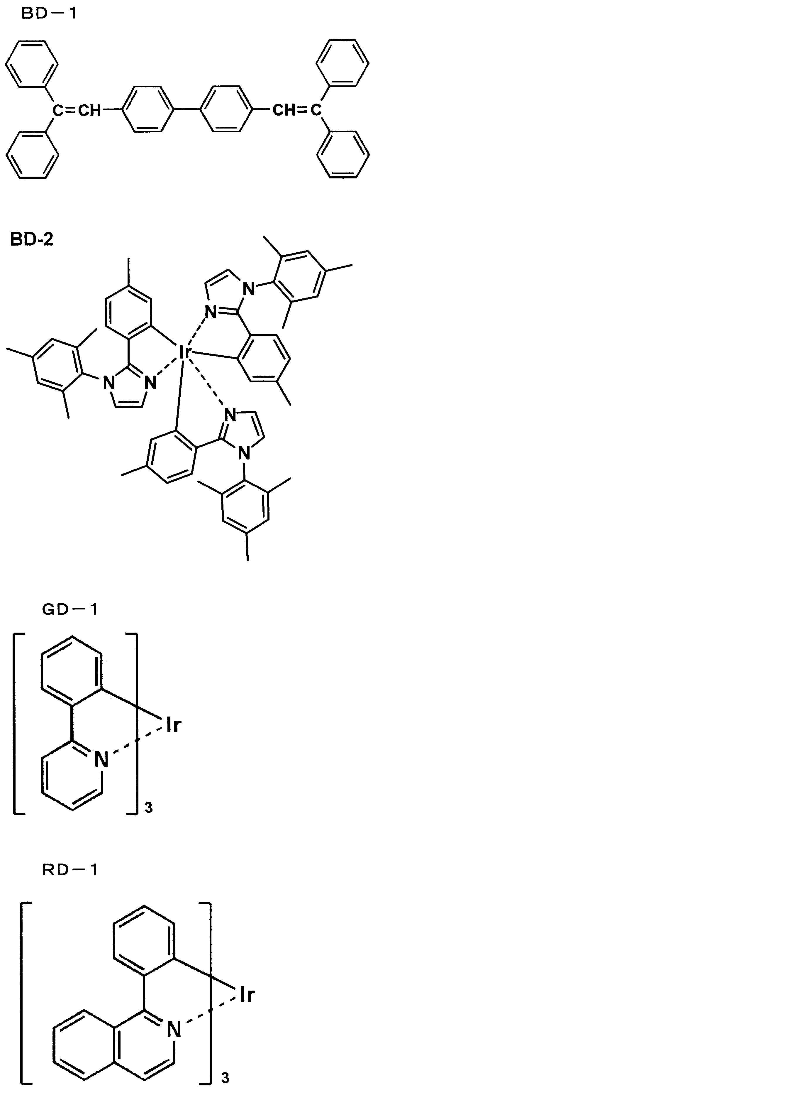
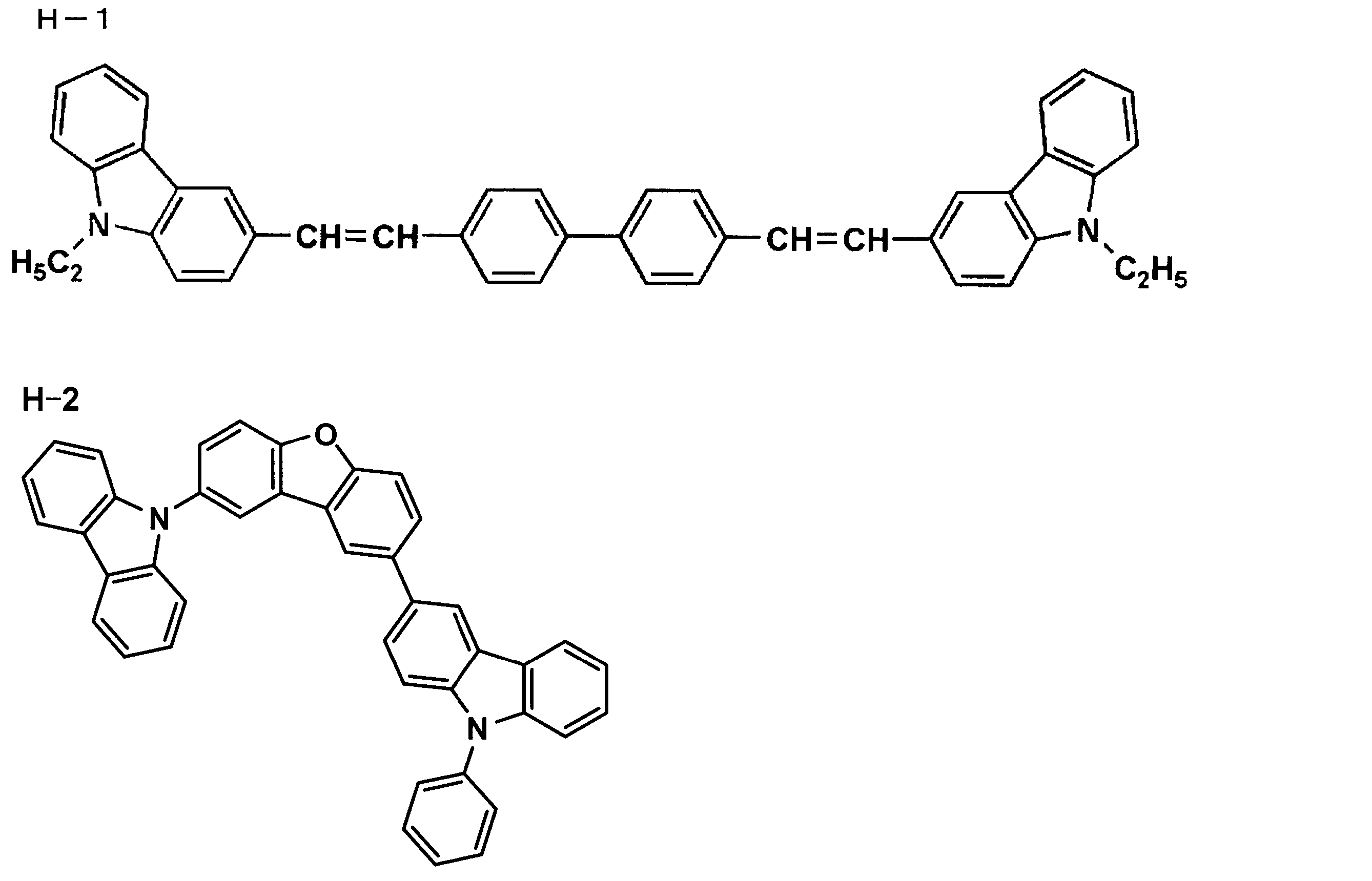

(1)有機EL素子101の作製
陽極として、30mm×30mm、厚さ0.7mmのガラス基板上に、ITO(インジウムチンオキシド)を150nmの厚さで製膜し、パターニングを行った後、このITO透明電極を付けた透明支持基板をイソプロピルアルコールで超音波洗浄し、乾燥窒素ガスで乾燥し、UVオゾン洗浄を5分間行った後、この透明支持基板を市販の真空蒸着装置の基板ホルダーに固定した。
次いで、化合物M-2を同様にして蒸着し、膜厚50nmの層を形成した。
次いで、化合物BD-1および化合物H-1を、化合物BD-1が5%の濃度になるように蒸着速度0.1nm/秒で共蒸着し、膜厚35nmの青色発光を呈する蛍光発光層を形成した。
次いで、化合物E―1を蒸着速度0.1nm/秒で蒸着し、膜厚25nmの層を形成した。
次いで、化合物M-2を蒸着速度0.1nm/秒で蒸着し、膜厚50nmの層を形成した。
次いで、化合物GD-1、RD-1および化合物H-2を、化合物GD-1が15%、RD-1が0.8%の濃度になるように蒸着速度0.1nm/秒で共蒸着し、膜厚30nmの黄色を呈するリン光発光層を形成した。
その後、化合物E―1を蒸着速度0.1nm/秒で蒸着し、膜厚35nmの層を形成した。
さらに、LiFを膜厚1.5nmで形成した後に、アルミニウム110nmを蒸着して陰極を形成した。
図2は有機EL素子の断面図を示している。図2に示すとおり、透明電極付きガラス基板107上に有機EL層106と陰極105とが積層・形成されている。ガラスカバー102内には窒素ガス108が充填され、捕水剤109が設けられている。
有機EL素子101の作製において、中間金属層の膜厚を1nmに変更した以外は同様にして「有機EL素子102」を作製した。
有機EL素子101の作製において、化合物E-1からなる層と中間金属層との間にLiFを厚さ1nmで製膜した以外は同様にして「有機EL素子103」を作製した。
有機EL素子102の作製において、化合物E-1からなる層と中間金属層との間にLiFを厚さ1nmで製膜した以外は同様にして「有機EL素子104」を作製した。
有機EL素子101の作製において、中間金属層を形成する材料をAgに変更した以外は同様にして「有機EL素子105」を作製した。
有機EL素子102の作製において、中間金属層を形成する材料をAgに変更した以外は同様にして「有機EL素子106」を作製した。
有機EL素子102の作製において、中間金属層を形成する材料をLiに変更した以外は同様にして「有機EL素子107」を作製した。
有機EL素子101の作製において、中間金属層を形成する材料をCaに変更した以外は同様にして「有機EL素子108」を作製した。
有機EL素子107の作製において、中間金属層の膜厚を4.5nmとした以外は同様にして「有機EL素子109」を作製した。
有機EL素子107の作製において、中間金属層の膜厚を2.5nmとした以外は同様にして「有機EL素子110」を作製した。
有機EL素子107の作製において、中間金属層の膜厚を1.5nmとした以外は同様にして「有機EL素子111」を作製した。
有機EL素子107の作製において、中間金属層の膜厚を1nmとした以外は同様にして「有機EL素子112」を作製した。
有機EL素子107の作製において、中間金属層の膜厚を0.7nmとした以外は同様にして「有機EL素子113」を作製した。
有機EL素子108の作製において、中間金属層の膜厚を1nmとした以外は同様にして「有機EL素子114」を作製した。
有機EL素子102の作製において、中間金属層を形成する材料をCsに変更した以外は同様にして「有機EL素子115」を作製した。
有機EL素子102の作製において、中間金属層を形成する材料をKに変更した以外は同様にして「有機EL素子116」を作製した。
(1)外部取出し発光量子効率、駆動電圧の測定
分光放射輝度計CS-2000(コニカミノルタセンシング社製)を用い、室温(25℃)にて各有機EL素子の正面輝度および輝度角度依存性を測定することにより、有機EL素子の基板前面から外部に放射される光量を計測し、通電量2.5mA/cm2における外部取出し発光量子収率を求め、また同通電量における駆動電圧を測定した。
評価結果を表1に示す。
なお、各有機EL素子の外部取出し発光量子効率および駆動電圧は、有機EL素子108の外部取出し発光量子効率および駆動電圧を100とした場合の相対値で示している。
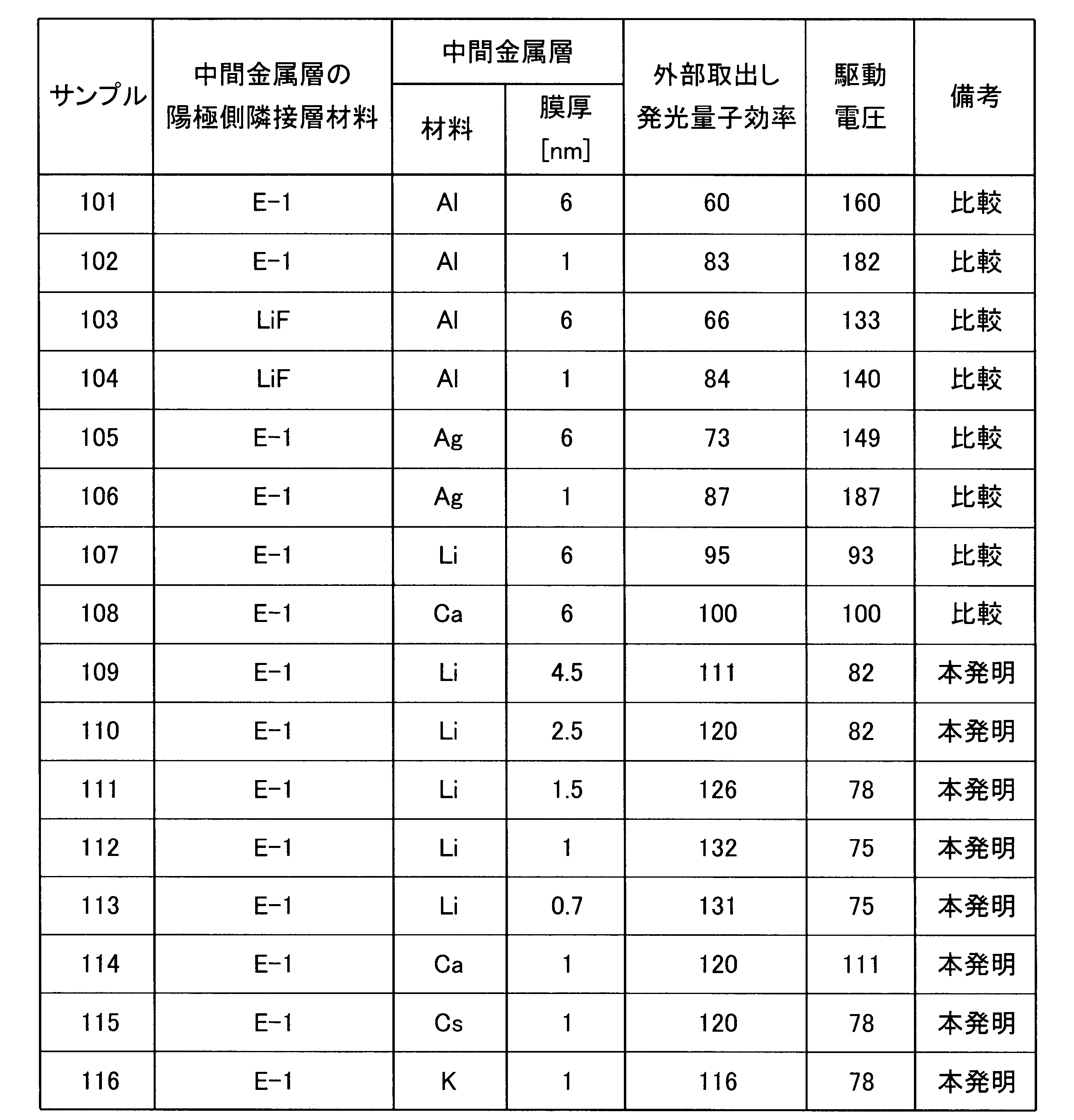
表1に示されるように、本発明の有機EL素子109~116は、比較例の有機EL素子101~108に対し、発光量子効率が向上しており、かつ、より低い電圧で駆動できることがわかる。
以上から、中間金属層として、仕事関数3.0eV以下の金属で構成し、その膜厚を0.6~5nmとすることが発光効率の向上および低電圧駆動に有用であることがわかる。
(1)有機EL素子201の作製
陽極として、30mm×30mm、厚さ0.7mmのガラス基板上に、ITO(インジウムチンオキシド)を150nmの厚さで製膜し、パターニングを行った後、このITO透明電極を付けた透明支持基板をイソプロピルアルコールで超音波洗浄し、乾燥窒素ガスで乾燥し、UVオゾン洗浄を5分間行った後、この透明支持基板を市販の真空蒸着装置の基板ホルダーに固定した。
次いで、化合物M-2を同様にして蒸着し、膜厚40nmの層を形成した。
次いで、化合物BD-1および化合物H-1を、化合物BD-1が5%の濃度になるように蒸着速度0.1nm/秒で共蒸着し、膜厚30nmの青色発光を呈する蛍光発光層を形成した。
次いで、化合物E-1を蒸着速度0.1nm/秒で蒸着し、膜厚30nmの層を形成した。
次いで、化合物M-2を蒸着速度0.1nm/秒で蒸着し、膜厚50nmの層を形成した。
次いで、化合物GD-1,RD-1および化合物H-2を、化合物GD-1が17%、RD-1が0.8%の濃度になるように蒸着速度0.1nm/秒で共蒸着し、膜厚30nmの黄色を呈するリン光発光層を形成した。
その後、化合物E-1を蒸着速度0.1nm/秒で蒸着し、膜厚30nmの層を形成した。
さらに、LiFを膜厚1.5nmにて形成した後に、アルミニウム110nmを蒸着して陰極を形成した。
有機EL素子201の作製において、中間金属層の膜厚をそれぞれ4.5nm、2.5nm、1.5nm、1nm、0.7nm、0.3nmとした以外は同様にして「有機EL素子202~207」を作製した。
有機EL素子201の作製において、中間金属層のLi膜厚を1nmとし、またLiFに変えてLiを膜厚1nmにて製膜した以外は同様にして「有機EL素子208」を作製した。
より詳しくは、発光ユニットを構成する化合物M-4で構成される層からリチウムで構成される中間金属層までの層構成およびその構成材料と、中間金属層の陰極側に隣接する化合物M-4で構成される層から陰極に隣接するリチウムで構成される層までの層構成およびその構成材料とが、発光層を除いて同一となっている。
(1)外部取出し発光量子効率、駆動電圧の測定
実施例1と同様にして、外部取出し発光量子効率、駆動電圧を評価した。
評価結果を表2に示す。
なお、各有機EL素子の外部取出し発光量子効率および駆動電圧は、有機EL素子201の外部取出し発光量子効率および駆動電圧を100とした場合の相対値で示している。
上記のように作製した有機EL素子201~208を90℃環境下で15時間保存(放置)し、2.5mA/cm2で駆動した際の保存前後での駆動電圧を室温(25℃)にて測定し、その変動幅を求め保存初期安定性の指標とした。
評価結果を表2に示す。
なお、各有機EL素子の駆動電圧の変動幅は、有機EL素子201の変動幅を100とした相対値で示している。
有機EL素子201~208を75℃環境下で500時間保存(放置)し、2.5mA/cm2で駆動した際の保存前後での駆動電圧、正面輝度を室温(25℃)にて測定し、その変動幅を求め長期保存安定性の指標とした。正面輝度は実施例1と同様に分光放射輝度計CS-2000(コニカミノルタセンシング社製)を用いて計測した。
評価結果を表2に示す。
なお、各有機EL素子の駆動電圧、正面輝度の変動幅は、有機EL素子201の変動幅を100とした相対値で示している。

表2に示すとおり、本発明の中間金属層の膜厚を有する有機EL素子202~206,208は、比較例の有機EL素子201,207と比較して、初期、長期保存いずれにおいても駆動電圧の変動が小さく、また長期保存での輝度変動が小さく良好であることがわかる。
詳しくは、中間金属層の膜厚が6nmと厚い比較例の有機EL素子201は、本発明の有機EL素子と比較して、特に長期保存における輝度変動が著しく大きい。また、中間金属層の膜厚が0.3nmと薄い比較例の有機EL素子207は、長期保存での輝度変動は本発明の有機EL素子と比較して顕著に劣位という訳ではないが、保存初期での駆動電圧変動が著しく大きく、安定性能において大きく劣っている。中間金属層の膜厚を本発明の範囲とすることで保存安定性が著しく向上することがわかる。
真空蒸着装置内の蒸着用るつぼの各々に、製膜材料を、各々試料作製に最適の量充填した。蒸着用るつぼはモリブデン製またはタングステン製の抵抗加熱用材料で作製されたものを用いた。
真空度1×10⁻⁴Paまで減圧した後、化合物E-1を蒸着速度0.1nm/秒で蒸着し、膜厚30nmの層を形成した。
次いで、リチウムを所望の膜厚に蒸着し、有機EL素子101と同様にして、上記素子の非発光面をガラスケースで覆い試料を作製した。
なお、中間金属層の膜厚が3nmを越えると、このような明暗模様は観察されず、中間金属層膜面が平坦であることを示した。
(1)有機EL素子401の作製
有機EL素子205の作製において、蛍光発光層に隣接して化合物E-1からなる層を製膜した後、KFを膜厚1.5nmに蒸着速度0.01nm/秒で製膜し、リチウムからなる中間金属層を形成した以外は同様にして「有機EL素子401」を作製した。
有機EL素子205の作製において、蛍光発光層に隣接して化合物E-1からなる層に変えて、化合物E-1とKFとを体積比85:15となるように蒸着速度0.1nm/秒で製膜した以外は同様にして「有機EL素子402」を作製した。
有機EL素子205の作製において、蛍光発光層に隣接して化合物E-1からなる層に変えて、化合物E-1とLiFとを体積比80:20となるように蒸着速度0.1nm/秒で製膜した以外は同様にして「有機EL素子403」を作製した。
実施例2と同様にして、駆動電圧、外部取出し発光量子効率および長期保存安定性を評価した。
評価結果を表3に示す。
なお、各有機EL素子の駆動電圧、外部取出し発光量子効率および長期保存安定性は、有機EL素子205の駆動電圧、外部取出し発光量子効率および長期保存安定性を100とした相対値で示している。
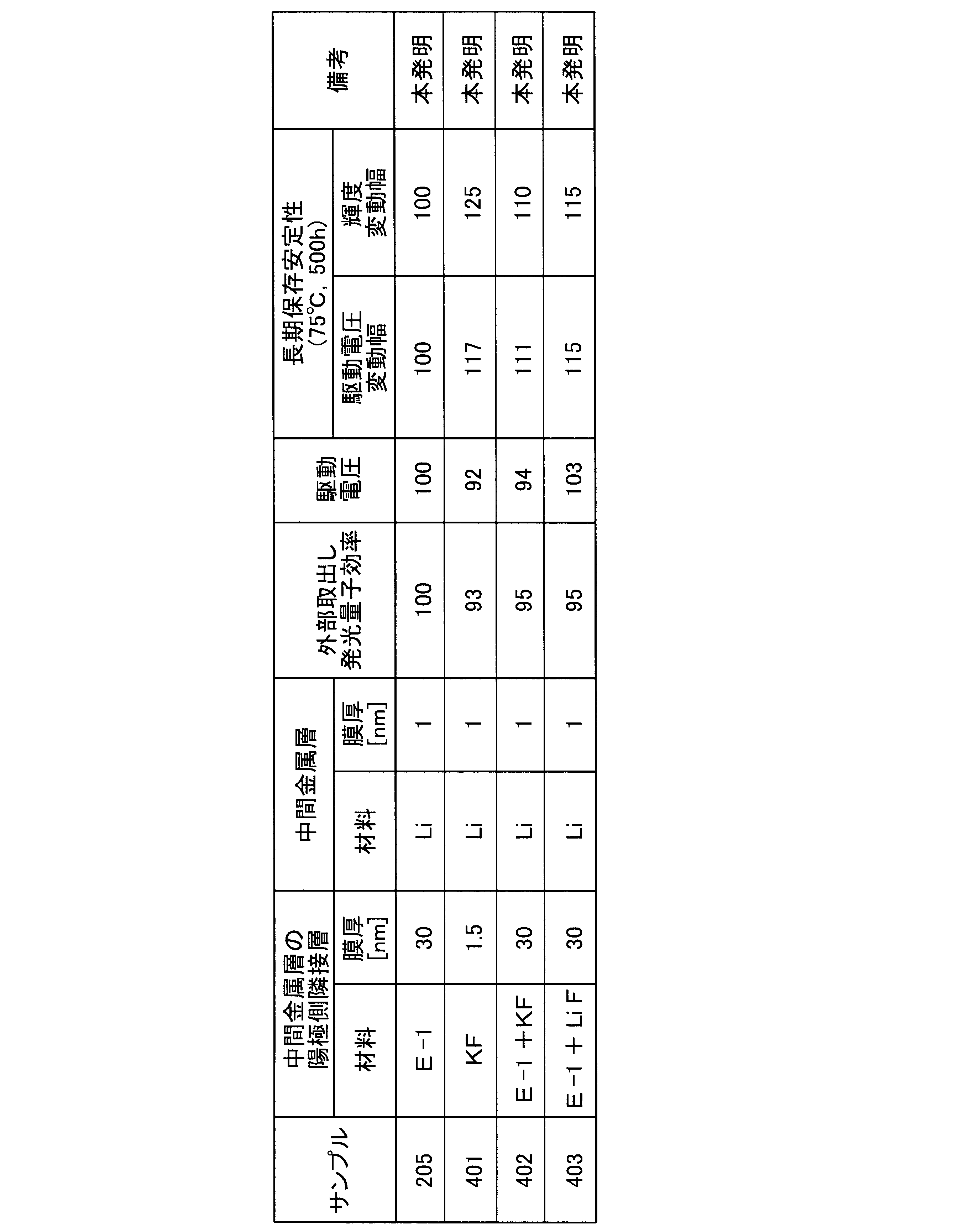
(1)有機EL素子501の作製
有機EL素子205の作製において、蛍光発光層に隣接して化合物E-1からなる層に変えて、化合物E-2からなる層を形成した以外は同様にして「有機EL素子501」を作製した。
有機EL素子501の作製において、化合物E-2からなる層を製膜した後、KFを膜厚1.5nmに蒸着速度0.01nm/秒で製膜し、リチウムからなる中間金属層を形成した以外は同様にして「有機EL素子502」を作製した。
実施例2と同様にして、駆動電圧、外部取出し発光量子効率および長期保存安定性を評価した。
評価結果を表4に示す。
なお、各有機EL素子の駆動電圧、外部取出し発光量子効率および長期保存安定性は、有機EL素子501の駆動電圧、外部取出し発光量子効率および長期保存安定性を100とした場合の相対値で示している。
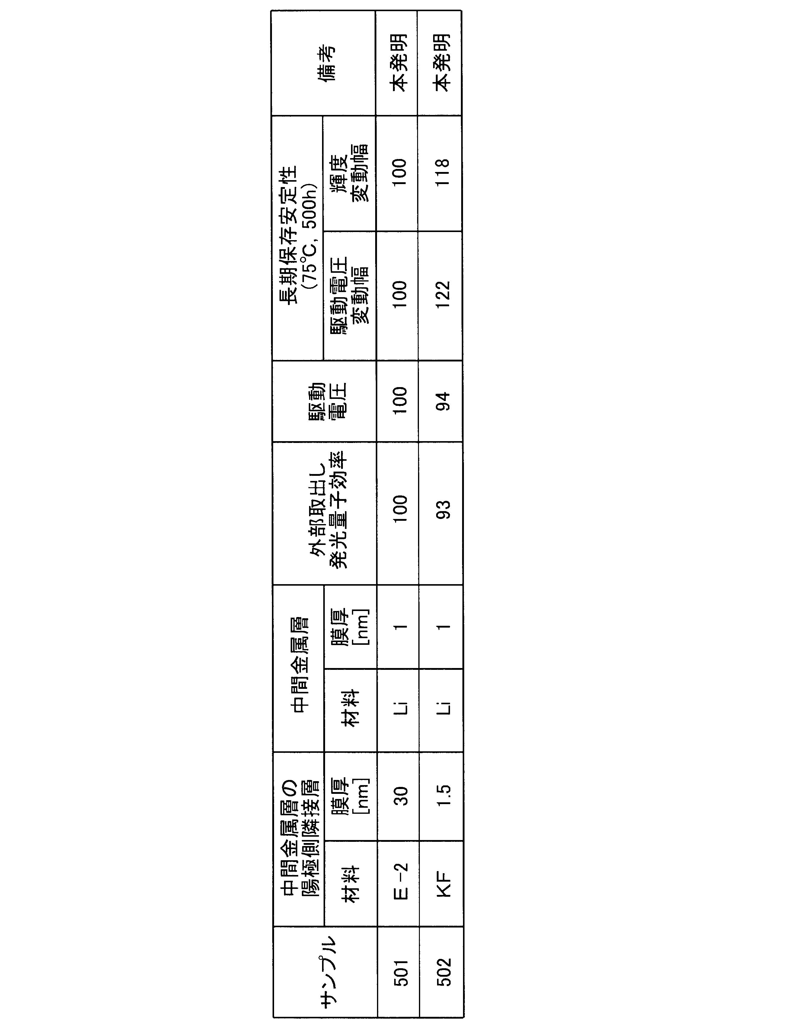
(1)有機EL素子601の作製
陽極として、30mm×30mm、厚さ0.7mmのガラス基板上に、ITO(インジウムチンオキシド)を150nmの厚さで製膜し、パターニングを行った後、このITO透明電極を付けた透明支持基板をイソプロピルアルコールで超音波洗浄し、乾燥窒素ガスで乾燥し、UVオゾン洗浄を5分間行った後、この透明支持基板を市販の真空蒸着装置の基板ホルダーに固定した。
次いで、化合物M-2を同様にして蒸着し、膜厚50nmの層を形成した。
次いで、化合物GD-1、RD-1および化合物H-2を、化合物GD-1が12%、RD-1が1.5%の濃度になるように蒸着速度0.1nm/秒で共蒸着し、膜厚12nmの黄色を呈するリン光発光層を形成した。
次いで、化合物BD-2および化合物H-2を、化合物BD-2が12%の濃度になるように蒸着速度0.1nm/秒で共蒸着し、膜厚20nmの青色発光を呈するリン光発光層を形成した。
次いで、化合物F-1を蒸着速度0.1nm/秒で蒸着し、膜厚5nmの層を形成し、さらに続いて、化合物E-1を蒸着速度0.1nm/秒で蒸着し、膜厚30nmの層を形成した。
有機EL素子601の作製において、中間金属層の膜厚を1nmとした以外は同様にして「有機EL素子602」を作製した。
有機EL素子601の作製において、中間金属層の膜厚を0.4nmとした以外は同様にして「有機EL素子603」を作製した。
実施例2と同様にして、駆動電圧、外部取出し発光量子効率および保存安定性を評価したところ、中間金属層の膜厚とこれら諸性能との関係において実施例2と同様の結果が得られ、全発光材料にリン光発光材料を使用した有機EL素子においても、本発明の効果が確認された。
(1)有機EL素子701の作製
陽極として、30mm×30mm、厚さ0.7mmのガラス基板上に、ITO(インジウムチンオキシド)を150nmの厚さで製膜し、パターニングを行った後、このITO透明電極を付けた透明支持基板をイソプロピルアルコールで超音波洗浄し、乾燥窒素ガスで乾燥し、UVオゾン洗浄を5分間行った後、この透明支持基板を市販の真空蒸着装置の基板ホルダーに固定した。
次いで、化合物M-2を同様にして蒸着し、膜厚50nmの層を形成した。
次いで、化合物GD-1および化合物H-2を、化合物GD-1が9%の濃度になるように蒸着速度0.1nm/秒で共蒸着し、膜厚30nmの緑色を呈するリン光発光層を形成した。
次いで、化合物E―1を蒸着速度0.1nm/秒で蒸着し、膜厚15nmの層を形成した。
その後、化合物GD-1、RD-1および化合物H-2を、化合物GD-1が8%、RD-1が1.5%の濃度になるように蒸着速度0.1nm/秒で共蒸着し、膜厚25nmの赤色を呈するリン光発光層を形成した。
次いで、化合物E-1を蒸着速度0.1nm/秒で蒸着し、膜厚25nmの層を形成した。
次いで、化合物BD-1および化合物H-1を、化合物BD-1が5%の濃度になるように蒸着速度0.1nm/秒で共蒸着し、膜厚25nmの青色発光を呈する蛍光発光層を形成した。
次いで、化合物E-1を蒸着速度0.1nm/秒で蒸着し、膜厚35nmの層を形成した。
さらに、リチウムを膜厚1nmにて形成した後に、アルミニウム110nmを蒸着して陰極を形成した。
有機EL素子701は、中間金属層を2カ所に有する素子である。
有機EL素子701の作製において、第1および第2中間金属層の膜厚を1nmとした以外は同様にして「有機EL素子702」を作製した。
有機EL素子701の作製において、第1および第2中間金属層の膜厚を0.4nmとした以外は同様にして「有機EL素子703」を作製した。
実施例2と同様にして、駆動電圧、外部取出し発光量子効率および保存安定性を評価したところ、中間金属層の膜厚とこれら諸性能との関係において実施例2と同様の結果が得られ、中間金属層を2カ所以上に有する有機EL素子においても、本発明の効果が確認された。
102 ガラスカバー
105 陰極
106 有機EL層
107 透明電極付きガラス基板
108 窒素ガス
109 捕水剤
110 明部
120 暗部
Claims (6)
- 陽極と陰極との間に、少なくとも1層の中間金属層と、少なくとも2つの発光ユニットと、を有し、前記中間金属層が2つの前記発光ユニット間に配置されている有機エレクトロルミネッセンス素子であって、
前記中間金属層が、仕事関数3.0eV以下の金属から構成され、かつ、膜厚が0.6~5nmであることを特徴とする有機エレクトロルミネッセンス素子。 - 前記中間金属層の前記発光ユニット側の少なくとも一方の側の表面が、非平坦面であることを特徴とする請求項1に記載の有機エレクトロルミネッセンス素子。
- 前記中間金属層の前記陽極側に隣接する層が、単一の有機化合物から構成されていることを特徴とする請求項1または2に記載の有機エレクトロルミネッセンス素子。
- 前記中間金属層の前記陽極側に隣接する層が、単一の有機化合物を製膜することにより形成されていることを特徴とする請求項1または2に記載の有機エレクトロルミネッセンス素子。
- 前記中間金属層と前記発光ユニットとで積層体とし、
前記積層体の層構成および各層の構成材料と、前記積層体の前記中間金属層側に隣接する他の発光ユニットまたは他の積層体の層構成および各層の構成材料とが、発光層を除いて同一であることを特徴とする請求項1に記載の有機エレクトロルミネッセンス素子。 - 白色発光を呈することを特徴とする請求項1に記載の有機エレクトロルミネッセンス素子。
Priority Applications (2)
| Application Number | Priority Date | Filing Date | Title |
|---|---|---|---|
| JP2014532886A JPWO2014034341A1 (ja) | 2012-08-27 | 2013-07-26 | 有機エレクトロルミネッセンス素子 |
| US14/424,143 US9379347B2 (en) | 2012-08-27 | 2013-07-26 | Organic electroluminescence element |
Applications Claiming Priority (2)
| Application Number | Priority Date | Filing Date | Title |
|---|---|---|---|
| JP2012186502 | 2012-08-27 | ||
| JP2012-186502 | 2012-08-27 |
Publications (1)
| Publication Number | Publication Date |
|---|---|
| WO2014034341A1 true WO2014034341A1 (ja) | 2014-03-06 |
Family
ID=50183161
Family Applications (1)
| Application Number | Title | Priority Date | Filing Date |
|---|---|---|---|
| PCT/JP2013/070355 Ceased WO2014034341A1 (ja) | 2012-08-27 | 2013-07-26 | 有機エレクトロルミネッセンス素子 |
Country Status (3)
| Country | Link |
|---|---|
| US (1) | US9379347B2 (ja) |
| JP (1) | JPWO2014034341A1 (ja) |
| WO (1) | WO2014034341A1 (ja) |
Families Citing this family (1)
| Publication number | Priority date | Publication date | Assignee | Title |
|---|---|---|---|---|
| KR102126544B1 (ko) * | 2013-12-30 | 2020-06-24 | 엘지디스플레이 주식회사 | 유기 전계 발광 소자 및 유기 전계 발광 표시 장치 |
Citations (6)
| Publication number | Priority date | Publication date | Assignee | Title |
|---|---|---|---|---|
| JP2006049393A (ja) * | 2004-07-30 | 2006-02-16 | Sanyo Electric Co Ltd | 有機エレクトロルミネッセント素子及び有機エレクトロルミネッセント表示装置 |
| JP2007149605A (ja) * | 2005-11-30 | 2007-06-14 | Sanyo Electric Co Ltd | 有機エレクトロルミネッセント素子及び有機エレクトロルミネッセント表示装置 |
| JP2007179933A (ja) * | 2005-12-28 | 2007-07-12 | Sanyo Electric Co Ltd | 有機エレクトロルミネッセント素子及び有機エレクトロルミネッセント表示装置 |
| JP2010003652A (ja) * | 2008-06-23 | 2010-01-07 | Panasonic Electric Works Co Ltd | 有機エレクトロルミネッセンス素子の製造方法 |
| JP2010192472A (ja) * | 2009-02-13 | 2010-09-02 | Sumitomo Chemical Co Ltd | 有機エレクトロルミネッセンス素子 |
| JP2011040437A (ja) * | 2009-08-06 | 2011-02-24 | Panasonic Electric Works Co Ltd | 有機エレクトロルミネッセンス素子 |
Family Cites Families (8)
| Publication number | Priority date | Publication date | Assignee | Title |
|---|---|---|---|---|
| US6337492B1 (en) | 1997-07-11 | 2002-01-08 | Emagin Corporation | Serially-connected organic light emitting diode stack having conductors sandwiching each light emitting layer |
| JP3884564B2 (ja) | 1998-05-20 | 2007-02-21 | 出光興産株式会社 | 有機el発光素子およびそれを用いた発光装置 |
| US20120007064A1 (en) * | 1999-12-31 | 2012-01-12 | Lg Chem, Ltd. | Organic electroluminescent device and method for preparing the same |
| JP2003264085A (ja) | 2001-12-05 | 2003-09-19 | Semiconductor Energy Lab Co Ltd | 有機半導体素子、有機エレクトロルミネッセンス素子及び有機太陽電池 |
| US6872472B2 (en) | 2002-02-15 | 2005-03-29 | Eastman Kodak Company | Providing an organic electroluminescent device having stacked electroluminescent units |
| US8951645B2 (en) | 2004-04-09 | 2015-02-10 | Lg Chem, Ltd. | Stacked organic light emitting device having high efficiency and high brightness |
| TWI382079B (zh) * | 2004-07-30 | 2013-01-11 | Sanyo Electric Co | 有機電場發光元件及有機電場發光顯示裝置 |
| DE602006001930D1 (de) | 2005-12-23 | 2008-09-04 | Novaled Ag | tur von organischen Schichten |
-
2013
- 2013-07-26 US US14/424,143 patent/US9379347B2/en not_active Expired - Fee Related
- 2013-07-26 JP JP2014532886A patent/JPWO2014034341A1/ja active Pending
- 2013-07-26 WO PCT/JP2013/070355 patent/WO2014034341A1/ja not_active Ceased
Patent Citations (6)
| Publication number | Priority date | Publication date | Assignee | Title |
|---|---|---|---|---|
| JP2006049393A (ja) * | 2004-07-30 | 2006-02-16 | Sanyo Electric Co Ltd | 有機エレクトロルミネッセント素子及び有機エレクトロルミネッセント表示装置 |
| JP2007149605A (ja) * | 2005-11-30 | 2007-06-14 | Sanyo Electric Co Ltd | 有機エレクトロルミネッセント素子及び有機エレクトロルミネッセント表示装置 |
| JP2007179933A (ja) * | 2005-12-28 | 2007-07-12 | Sanyo Electric Co Ltd | 有機エレクトロルミネッセント素子及び有機エレクトロルミネッセント表示装置 |
| JP2010003652A (ja) * | 2008-06-23 | 2010-01-07 | Panasonic Electric Works Co Ltd | 有機エレクトロルミネッセンス素子の製造方法 |
| JP2010192472A (ja) * | 2009-02-13 | 2010-09-02 | Sumitomo Chemical Co Ltd | 有機エレクトロルミネッセンス素子 |
| JP2011040437A (ja) * | 2009-08-06 | 2011-02-24 | Panasonic Electric Works Co Ltd | 有機エレクトロルミネッセンス素子 |
Also Published As
| Publication number | Publication date |
|---|---|
| JPWO2014034341A1 (ja) | 2016-08-08 |
| US9379347B2 (en) | 2016-06-28 |
| US20150243921A1 (en) | 2015-08-27 |
Similar Documents
| Publication | Publication Date | Title |
|---|---|---|
| JP5359869B2 (ja) | 有機エレクトロルミネッセンス素子、有機エレクトロルミネッセンス素子の製造方法、表示装置及び照明装置 | |
| JP5533652B2 (ja) | 白色発光有機エレクトロルミネッセンス素子、照明装置及び表示装置 | |
| JP5381719B2 (ja) | 白色発光有機エレクトロルミネッセンス素子 | |
| JP5499890B2 (ja) | 有機エレクトロルミネッセンス素子、及びその製造方法 | |
| JP5163642B2 (ja) | 有機エレクトロルミネセンス素子 | |
| JP6225915B2 (ja) | 有機エレクトロルミネッセンス素子 | |
| JP6107657B2 (ja) | 有機エレクトロルミネッセンス素子 | |
| JP2013110262A (ja) | 有機el素子ならびに有機elモジュールおよびその製造方法 | |
| JP2007311460A (ja) | 有機エレクトロルミネッセンス素子材料、有機エレクトロルミネッセンス素子、表示装置及び照明装置 | |
| JP5521753B2 (ja) | 有機エレクトロルミネッセンス素子 | |
| JP2011009517A (ja) | 有機エレクトロルミネッセンス素子 | |
| JP5636630B2 (ja) | 有機エレクトロルミネッセンス素子材料、有機エレクトロルミネッセンス素子、表示装置及び照明装置 | |
| JP5353006B2 (ja) | 有機エレクトロルミネッセンス素子、液晶表示装置及び照明装置 | |
| JP2007059310A (ja) | 有機エレクトロルミネッセンス素子、照明装置 | |
| JP2008235503A (ja) | 有機エレクトロルミネッセンス素子及びそれを用いた照明装置 | |
| JP2013172071A (ja) | 有機エレクトロルミネッセンス素子及び照明装置 | |
| JP2013102006A (ja) | 有機el素子 | |
| JP5320881B2 (ja) | 有機エレクトロルミネッセンス素子、表示装置、照明装置及び有機エレクトロルミネッセンス素子材料 | |
| US9379347B2 (en) | Organic electroluminescence element | |
| JP6197650B2 (ja) | 有機el素子 | |
| JP5835217B2 (ja) | 有機エレクトロルミネッセンス素子 | |
| JP2013089608A (ja) | 有機el素子 | |
| JP4923651B2 (ja) | 有機エレクトロルミネッセンス素子、表示装置及び照明装置 | |
| WO2015111489A1 (ja) | 有機エレクトロルミネッセンス素子 | |
| JP2008047428A (ja) | 有機エレクトロルミネッセンス素子の製造方法、有機エレクトロルミネッセンス素子、照明装置及びディスプレイ装置 |
Legal Events
| Date | Code | Title | Description |
|---|---|---|---|
| 121 | Ep: the epo has been informed by wipo that ep was designated in this application |
Ref document number: 13834151 Country of ref document: EP Kind code of ref document: A1 |
|
| ENP | Entry into the national phase |
Ref document number: 2014532886 Country of ref document: JP Kind code of ref document: A |
|
| WWE | Wipo information: entry into national phase |
Ref document number: 14424143 Country of ref document: US |
|
| NENP | Non-entry into the national phase |
Ref country code: DE |
|
| 122 | Ep: pct application non-entry in european phase |
Ref document number: 13834151 Country of ref document: EP Kind code of ref document: A1 |