WO2014030239A1 - 薄膜トランジスタおよびその製造方法 - Google Patents
薄膜トランジスタおよびその製造方法 Download PDFInfo
- Publication number
- WO2014030239A1 WO2014030239A1 PCT/JP2012/071297 JP2012071297W WO2014030239A1 WO 2014030239 A1 WO2014030239 A1 WO 2014030239A1 JP 2012071297 W JP2012071297 W JP 2012071297W WO 2014030239 A1 WO2014030239 A1 WO 2014030239A1
- Authority
- WO
- WIPO (PCT)
- Prior art keywords
- thin film
- carbon nanowall
- film transistor
- electrode
- silicon substrate
- Prior art date
- Legal status (The legal status is an assumption and is not a legal conclusion. Google has not performed a legal analysis and makes no representation as to the accuracy of the status listed.)
- Ceased
Links
Images


















Classifications
-
- H—ELECTRICITY
- H10—SEMICONDUCTOR DEVICES; ELECTRIC SOLID-STATE DEVICES NOT OTHERWISE PROVIDED FOR
- H10D—INORGANIC ELECTRIC SEMICONDUCTOR DEVICES
- H10D30/00—Field-effect transistors [FET]
- H10D30/60—Insulated-gate field-effect transistors [IGFET]
- H10D30/67—Thin-film transistors [TFT]
- H10D30/674—Thin-film transistors [TFT] characterised by the active materials
- H10D30/6741—Group IV materials, e.g. germanium or silicon carbide
- H10D30/6748—Group IV materials, e.g. germanium or silicon carbide having a multilayer structure or superlattice structure
-
- H—ELECTRICITY
- H10—SEMICONDUCTOR DEVICES; ELECTRIC SOLID-STATE DEVICES NOT OTHERWISE PROVIDED FOR
- H10D—INORGANIC ELECTRIC SEMICONDUCTOR DEVICES
- H10D30/00—Field-effect transistors [FET]
- H10D30/01—Manufacture or treatment
-
- H—ELECTRICITY
- H10—SEMICONDUCTOR DEVICES; ELECTRIC SOLID-STATE DEVICES NOT OTHERWISE PROVIDED FOR
- H10D—INORGANIC ELECTRIC SEMICONDUCTOR DEVICES
- H10D30/00—Field-effect transistors [FET]
- H10D30/01—Manufacture or treatment
- H10D30/021—Manufacture or treatment of FETs having insulated gates [IGFET]
- H10D30/031—Manufacture or treatment of FETs having insulated gates [IGFET] of thin-film transistors [TFT]
-
- H—ELECTRICITY
- H10—SEMICONDUCTOR DEVICES; ELECTRIC SOLID-STATE DEVICES NOT OTHERWISE PROVIDED FOR
- H10D—INORGANIC ELECTRIC SEMICONDUCTOR DEVICES
- H10D30/00—Field-effect transistors [FET]
- H10D30/40—FETs having zero-dimensional [0D], one-dimensional [1D] or two-dimensional [2D] charge carrier gas channels
- H10D30/47—FETs having zero-dimensional [0D], one-dimensional [1D] or two-dimensional [2D] charge carrier gas channels having two-dimensional [2D] charge carrier gas channels, e.g. nanoribbon FETs or high electron mobility transistors [HEMT]
-
- H—ELECTRICITY
- H10—SEMICONDUCTOR DEVICES; ELECTRIC SOLID-STATE DEVICES NOT OTHERWISE PROVIDED FOR
- H10D—INORGANIC ELECTRIC SEMICONDUCTOR DEVICES
- H10D30/00—Field-effect transistors [FET]
- H10D30/40—FETs having zero-dimensional [0D], one-dimensional [1D] or two-dimensional [2D] charge carrier gas channels
- H10D30/47—FETs having zero-dimensional [0D], one-dimensional [1D] or two-dimensional [2D] charge carrier gas channels having two-dimensional [2D] charge carrier gas channels, e.g. nanoribbon FETs or high electron mobility transistors [HEMT]
- H10D30/471—High electron mobility transistors [HEMT] or high hole mobility transistors [HHMT]
- H10D30/477—Vertical HEMTs or vertical HHMTs
-
- H—ELECTRICITY
- H10—SEMICONDUCTOR DEVICES; ELECTRIC SOLID-STATE DEVICES NOT OTHERWISE PROVIDED FOR
- H10D—INORGANIC ELECTRIC SEMICONDUCTOR DEVICES
- H10D30/00—Field-effect transistors [FET]
- H10D30/40—FETs having zero-dimensional [0D], one-dimensional [1D] or two-dimensional [2D] charge carrier gas channels
- H10D30/47—FETs having zero-dimensional [0D], one-dimensional [1D] or two-dimensional [2D] charge carrier gas channels having two-dimensional [2D] charge carrier gas channels, e.g. nanoribbon FETs or high electron mobility transistors [HEMT]
- H10D30/471—High electron mobility transistors [HEMT] or high hole mobility transistors [HHMT]
- H10D30/478—High electron mobility transistors [HEMT] or high hole mobility transistors [HHMT] the 2D charge carrier gas being at least partially not parallel to a main surface of the semiconductor body
-
- H—ELECTRICITY
- H10—SEMICONDUCTOR DEVICES; ELECTRIC SOLID-STATE DEVICES NOT OTHERWISE PROVIDED FOR
- H10D—INORGANIC ELECTRIC SEMICONDUCTOR DEVICES
- H10D30/00—Field-effect transistors [FET]
- H10D30/60—Insulated-gate field-effect transistors [IGFET]
- H10D30/67—Thin-film transistors [TFT]
- H10D30/6729—Thin-film transistors [TFT] characterised by the electrodes
- H10D30/673—Thin-film transistors [TFT] characterised by the electrodes characterised by the shapes, relative sizes or dispositions of the gate electrodes
-
- H—ELECTRICITY
- H10—SEMICONDUCTOR DEVICES; ELECTRIC SOLID-STATE DEVICES NOT OTHERWISE PROVIDED FOR
- H10D—INORGANIC ELECTRIC SEMICONDUCTOR DEVICES
- H10D30/00—Field-effect transistors [FET]
- H10D30/60—Insulated-gate field-effect transistors [IGFET]
- H10D30/67—Thin-film transistors [TFT]
- H10D30/674—Thin-film transistors [TFT] characterised by the active materials
- H10D30/6741—Group IV materials, e.g. germanium or silicon carbide
-
- H—ELECTRICITY
- H10—SEMICONDUCTOR DEVICES; ELECTRIC SOLID-STATE DEVICES NOT OTHERWISE PROVIDED FOR
- H10D—INORGANIC ELECTRIC SEMICONDUCTOR DEVICES
- H10D30/00—Field-effect transistors [FET]
- H10D30/60—Insulated-gate field-effect transistors [IGFET]
- H10D30/67—Thin-film transistors [TFT]
- H10D30/6757—Thin-film transistors [TFT] characterised by the structure of the channel, e.g. transverse or longitudinal shape or doping profile
-
- H—ELECTRICITY
- H10—SEMICONDUCTOR DEVICES; ELECTRIC SOLID-STATE DEVICES NOT OTHERWISE PROVIDED FOR
- H10D—INORGANIC ELECTRIC SEMICONDUCTOR DEVICES
- H10D30/00—Field-effect transistors [FET]
- H10D30/60—Insulated-gate field-effect transistors [IGFET]
- H10D30/67—Thin-film transistors [TFT]
- H10D30/6758—Thin-film transistors [TFT] characterised by the insulating substrates
-
- H—ELECTRICITY
- H10—SEMICONDUCTOR DEVICES; ELECTRIC SOLID-STATE DEVICES NOT OTHERWISE PROVIDED FOR
- H10D—INORGANIC ELECTRIC SEMICONDUCTOR DEVICES
- H10D62/00—Semiconductor bodies, or regions thereof, of devices having potential barriers
- H10D62/10—Shapes, relative sizes or dispositions of the regions of the semiconductor bodies; Shapes of the semiconductor bodies
- H10D62/17—Semiconductor regions connected to electrodes not carrying current to be rectified, amplified or switched, e.g. channel regions
- H10D62/213—Channel regions of field-effect devices
- H10D62/221—Channel regions of field-effect devices of FETs
- H10D62/235—Channel regions of field-effect devices of FETs of IGFETs
-
- H—ELECTRICITY
- H10—SEMICONDUCTOR DEVICES; ELECTRIC SOLID-STATE DEVICES NOT OTHERWISE PROVIDED FOR
- H10D—INORGANIC ELECTRIC SEMICONDUCTOR DEVICES
- H10D62/00—Semiconductor bodies, or regions thereof, of devices having potential barriers
- H10D62/80—Semiconductor bodies, or regions thereof, of devices having potential barriers characterised by the materials
- H10D62/83—Semiconductor bodies, or regions thereof, of devices having potential barriers characterised by the materials being Group IV materials, e.g. B-doped Si or undoped Ge
- H10D62/8303—Diamond
-
- H—ELECTRICITY
- H10—SEMICONDUCTOR DEVICES; ELECTRIC SOLID-STATE DEVICES NOT OTHERWISE PROVIDED FOR
- H10D—INORGANIC ELECTRIC SEMICONDUCTOR DEVICES
- H10D62/00—Semiconductor bodies, or regions thereof, of devices having potential barriers
- H10D62/80—Semiconductor bodies, or regions thereof, of devices having potential barriers characterised by the materials
- H10D62/881—Semiconductor bodies, or regions thereof, of devices having potential barriers characterised by the materials being a two-dimensional material
- H10D62/882—Graphene
Definitions
- the present invention relates to a thin film transistor and a method for manufacturing the same.
- Patent Document 1 a vertical current drive device using a carbon nanowall is known.
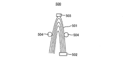
- FIG. 50 is a schematic diagram of a conventional vertical current drive device.
- a conventional vertical current drive device 500 includes a carbon nanowall 501, a source electrode 502, a drain electrode 503, and a gate electrode 504.
- the carbon nanowall 501 has a structure in which several layers of graphene sheets are stacked.
- the source electrode 502 is disposed at one end of the carbon nanowall 501, and the drain electrode 503 is disposed in contact with the outermost surface or the lowermost surface of the carbon nanowall 401 at the top of the carbon nanowall 501.
- the gate electrode 504 is disposed in contact with the outermost surface of the carbon nanowall 501.
- Patent Document 1 does not describe a method for controlling the orientation of carbon nanowalls, it is difficult to configure a channel layer of a vertical current driving device with a plurality of carbon nanowalls. There is a problem that it is difficult to flow a larger current through the vertical current driving device than in the case of a single carbon nanowall.
- an object of the present invention is to provide a thin film transistor capable of flowing a larger current than in the case where the channel layer is made of one carbon nanowall. is there.
- Another object of the present invention is to provide a method of manufacturing a thin film transistor capable of flowing a larger current than when the channel layer is made of one carbon nanowall.
- the thin film transistor includes a silicon substrate, a channel layer, a source electrode, a drain electrode, a gate electrode, and an insulating film.
- the silicon substrate has a concavo-convex shape formed on one main surface in a stripe or grid pattern.
- the channel layer is composed of a plurality of carbon nanowall thin films that are arranged on the plurality of protrusions along the length direction of the protrusions having the concavo-convex shape, and each grows in the normal direction of the silicon substrate.
- the source electrode is at least in contact with the first side surface parallel to the thickness direction of the carbon nanowall thin film in each of the plurality of carbon nanowall thin films.
- the drain electrode is disposed so as to face the source electrode in the in-plane direction of the carbon nanowall thin film, and at least is in contact with the second side face facing the first side face in each of the plurality of carbon nanowall thin films.
- the insulating film is disposed between the plurality of carbon nanowall thin films and the gate electrode.
- the thin film transistor manufacturing method is a method of manufacturing a thin film transistor using a plurality of carbon nanowall thin films as a channel layer.
- a first step of forming a grid pattern a second step of forming a plurality of carbon nanowall thin films on the plurality of convex portions along the length direction of the convex portions having the concavo-convex shape, and a plurality of carbon nano
- a third step of forming a source electrode so as to be in contact with at least a first side surface parallel to the thickness direction of the carbon nanowall thin film in each of the wall thin films, and facing the source electrode in the in-plane direction of the carbon nanowall thin film
- Each of the plurality of carbon nanowall thin films is in contact with at least a second side opposite to the first side.
- a plurality of carbon nanowall thin films constituting the channel layer are arranged in parallel between the source electrode and the drain electrode.
- the thin film transistor manufacturing method manufactures a thin film transistor such that a plurality of carbon nanowall thin films constituting the channel layer are arranged in parallel between the source electrode and the drain electrode.
- a larger current can flow than when the channel layer is formed of one carbon nanowall thin film.
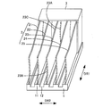
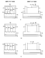
- FIG. 3 is a perspective view of a silicon substrate, a channel layer, and a source electrode shown in FIGS. 1 and 2.
- FIG. 5 is a plan view of a planar conductor, a feeding electrode, and a termination electrode viewed from the matching circuit side shown in FIG. 4.
- FIG. 4 is sectional drawing of a planar conductor of a Y direction, and a figure which shows plasma density.
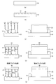
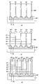
- FIG. 3 is a first process diagram illustrating a method for manufacturing the thin film transistor illustrated in FIGS. 1 and 2.
- FIG. 3 is a second process diagram illustrating a method of manufacturing the thin film transistor illustrated in FIGS. 1 and 2.
- FIG. 6 is a perspective view showing another silicon substrate in the first embodiment. It is a conceptual diagram of the carbon nanowall thin film formed on the silicon substrate shown in FIG.
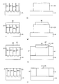
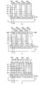
- FIG. 10 is a first process diagram showing a method for manufacturing a thin film transistor when the silicon substrate shown in FIG. 9 is used.
- FIG. 10 is a second process diagram illustrating a method for manufacturing the thin film transistor when the silicon substrate illustrated in FIG. 9 is used.
- FIG. 10 is a third process diagram illustrating the method for manufacturing the thin film transistor when the silicon substrate illustrated in FIG. 9 is used.
- FIG. 10 is a third process diagram illustrating the method for manufacturing the thin film transistor when the silicon substrate illustrated in FIG. 9 is used.
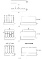
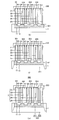
- FIG. 3 is a first process diagram showing another method for manufacturing the thin film transistor shown in FIGS. 1 and 2.
- FIG. 4 is a second process diagram illustrating another method for manufacturing the thin film transistor illustrated in FIGS. 1 and 2.
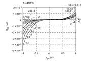
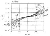
- FIG. 3 is a diagram showing electrical characteristics of the thin film transistor in Example 1. It is a figure which shows the electrical property of the thin-film transistor in Example 2.
- FIG. It is a figure which shows the electrical property of the thin-film transistor in Example 4.
- FIG. It is a SEM (photograph of the area
- 6 is a plan view showing a configuration of another thin film transistor according to Embodiment 1.
- FIG. 6 is a cross-sectional view illustrating a configuration of a thin film transistor according to a second embodiment.
- FIG. 23 is a plan view of the thin film transistor viewed from the A direction illustrated in FIG. 22.
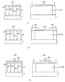
- FIG. 24 is a first process diagram illustrating a method of manufacturing the thin film transistor illustrated in FIGS. 22 and 23.
- FIG. 24 is a second process diagram illustrating the method of manufacturing the thin film transistor illustrated in FIGS. 22 and 23.
- FIG. 24 is a third process diagram illustrating the method for manufacturing the thin film transistor illustrated in FIGS. 22 and 23.
- FIG. 24 is a first process diagram illustrating another method for manufacturing the thin film transistor illustrated in FIGS. 22 and 23.
- FIG. 24 is a second process diagram illustrating another method for manufacturing the thin film transistor illustrated in FIGS.
- FIG. 24 is a third process diagram illustrating another method for manufacturing the thin film transistor illustrated in FIGS. 22 and 23.
- FIG. 24 is a fourth process diagram illustrating another method for manufacturing the thin film transistor illustrated in FIGS. 22 and 23.
- FIG. 24 is a first process diagram illustrating yet another method of manufacturing the thin film transistor illustrated in FIGS. 22 and 23.
- FIG. 24 is a second process diagram illustrating yet another method of manufacturing the thin film transistor illustrated in FIGS. 22 and 23.
- FIG. 24 is a third process diagram illustrating yet another method of manufacturing the thin film transistor illustrated in FIGS. 22 and 23.
- FIG. 10 is a plan view showing a configuration of another thin film transistor according to the second embodiment.
- FIG. 6 is a cross-sectional view illustrating a configuration of a thin film transistor according to a third embodiment.
- FIG. 36 is a first process diagram showing a method of manufacturing the thin film transistor shown in FIG. 35.
- FIG. 36 is a second process diagram illustrating the method of manufacturing the thin film transistor illustrated in FIG. 35.
- FIG. 36 is a third process diagram illustrating the method of manufacturing the thin film transistor illustrated in FIG. 35.
- FIG. 36 is a fourth process chart showing the method for manufacturing the thin film transistor shown in FIG. 35.
- FIG. 36 is a first process diagram showing another method for manufacturing the thin film transistor shown in FIG. 35.
- FIG. 36 is a second process diagram illustrating another method for manufacturing the thin film transistor illustrated in FIG. 35.
- FIG. 36 is a third process diagram illustrating another method for manufacturing the thin film transistor illustrated in FIG. 35.
- FIG. 36 is a fourth process diagram illustrating another method for manufacturing the thin film transistor illustrated in FIG. 35.
- FIG. 36 is a fifth process diagram illustrating another method for manufacturing the thin film transistor illustrated in FIG. 35.
- FIG. 36 is a first process diagram showing yet another method for manufacturing the thin film transistor shown in FIG. 35.
- FIG. 36 is a second process diagram illustrating yet another method of manufacturing the thin film transistor illustrated in FIG. 35.
- FIG. 36 is a third process diagram illustrating yet another method of manufacturing the thin film transistor illustrated in FIG. 35.
- FIG. 36 is a fourth process diagram illustrating yet another method of manufacturing the thin film transistor illustrated in FIG. 35.
- FIG. 10 is a cross-sectional view showing a configuration of another thin film transistor according to Embodiment 3. It is the schematic of the conventional vertical type current drive device.
- FIG. 1 is a cross-sectional view showing a configuration of a thin film transistor according to Embodiment 1 of the present invention.
- 2 is a plan view of the thin film transistor viewed from the direction A shown in FIG.
- a thin film transistor 10 includes a silicon substrate 1, a channel layer 2, a source electrode 3, a drain electrode 4, an insulating film 5, and a gate electrode 6. With.
- the silicon substrate 1 is made of any one of n-type single crystal silicon, p-type single crystal silicon, n-type polycrystalline silicon, and p-type polycrystalline silicon.
- the silicon substrate 1 has a specific resistance of 0.1 to 1 ⁇ ⁇ cm, for example.
- the channel layer 2 is disposed on one main surface of the silicon substrate 1.
- the channel layer 2 is composed of a plurality of carbon nanowall thin films 21 to 25.
- the carbon nanowall thin films 21 to 25 are disposed substantially perpendicular to the silicon substrate 1 and are disposed substantially parallel to each other.
- the source electrode 3 is disposed in contact with one end of the channel layer 2 in the in-plane direction of the silicon substrate 1.
- the drain electrode 4 is disposed in contact with the other end of the channel layer 2 so as to face the source electrode 3 in the in-plane direction of the silicon substrate 1.
- the source electrode 3 and the drain electrode 4 are disposed in contact with the carbon nanowall thin films 21 to 25, respectively.
- the insulating film 5 is made of, for example, silicon dioxide (SiO 2 ).
- the insulating film 5 is disposed in contact with the surface of the silicon substrate 1 opposite to the one main surface where the channel layer 2 is disposed.
- the gate electrode 6 is disposed in contact with the insulating film 5.
- Each of the source electrode 3, the drain electrode 4, and the gate electrode 6 has a laminated structure of Ti / Au, for example. And the thickness of Ti is 10 nm, for example, and the thickness of Au is 20 nm, for example.
- FIG. 3 is a perspective view of the silicon substrate 1, the channel layer 2, and the source electrode 3 shown in FIGS.
- silicon substrate 1 includes a convex portion 11 and a concave portion 12.
- the convex portion 11 and the concave portion 12 are formed on one main surface of the silicon substrate 1 along the direction DR1.
- the lengths of the convex portion 11 and the concave portion 12 in the direction DR1 may be the same as the length of the silicon substrate 1 or may be shorter than the length of the silicon substrate 1.
- the convex portions 11 and the concave portions 12 are alternately formed in the direction DR2 perpendicular to the direction DR1.
- the convex portion 11 has a length of 0.1 to 0.5 ⁇ m in the direction DR2.
- Recess 12 has a length of 0.6 to 1.5 ⁇ m in direction DR2.
- the convex portion 11 has a width of 0.1 to 0.5 ⁇ m
- the concave portion 12 has a width of 0.6 to 1.5 ⁇ m.
- the silicon substrate 1 has a concavo-convex shape arranged in a stripe shape on one main surface.
- Each of the carbon nanowall thin films 21 to 25 has a thickness of 10 to 15 nm and a height of 60 to 2500 nm.
- the plurality of carbon nanowall thin films 21 to 25 are arranged along the length direction of the convex portion 11 of the silicon substrate 1. That is, the plurality of carbon nanowall thin films 21 to 25 are oriented along a desired pattern.
- the source electrode 3 is disposed on the silicon substrate 1 so as to cover one ends of the plurality of carbon nanowall thin films 21 to 25.
- the source electrode 3 is in contact with the side surface 23 ⁇ / b> A and the upper surface 23 ⁇ / b> C parallel to the thickness direction of the carbon nanowall thin film 23 on one end side of the carbon nanowall thin film 23.
- the source electrode 3 is in contact with at least the side surface 23A parallel to the thickness direction of the carbon nanowall thin films 21 to 25 in each of the plurality of carbon nanowall thin films 21 to 25.
- the drain electrode 4 is at least in contact with the side surface 23B facing the side surface 23A parallel to the thickness direction of the carbon nanowall thin films 21 to 25 in each of the plurality of carbon nanowall thin films 21 to 25.
- the source electrode 3 and the drain electrode 4 sandwich the carbon nanowall thin films 21 to 25 from the direction DR1 in which the convex portions 11 and the concave portions 12 are formed.
- the source electrode 3 and the drain electrode 4 are at least in contact with the opposing side surfaces 23A and 23B of the carbon nanowall thin films 21 to 25.
- the thin film transistor 10 is a thin film transistor using the plurality of carbon nanowall thin films 21 to 25 as the channel layer 2.
- the thin film transistor 10 is a back gate type thin film transistor in which the gate electrode 6 is disposed below the channel layer 2.
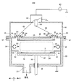
- FIG. 4 is a cross-sectional view showing a configuration of a plasma apparatus for producing the plurality of carbon nanowall thin films 21 to 25 shown in FIG.
- the plasma apparatus 100 includes a vacuum vessel 20, a top plate 26, an exhaust port 27, a gas introduction unit 28, a holder 32, a heater 34, a shaft 36, a bearing unit 38, A mask 42, a partition plate 44, a planar conductor 50, a feeding electrode 52, a termination electrode 54, an insulating flange 56, packings 57 and 58, a shield box 60, a high frequency power supply 62, a matching circuit 64, Connection conductors 68 and 69 are provided.
- the vacuum vessel 20 is made of metal, and is connected to the vacuum exhaust device via the exhaust port 27.
- the vacuum vessel 20 is electrically connected to the ground node.
- the top plate 26 is disposed in contact with the vacuum vessel 20 so as to close the upper side of the vacuum vessel 20.
- a vacuum seal packing 57 is disposed between the vacuum vessel 20 and the top plate 26.
- the gas introduction unit 28 is disposed above the partition plate 44 in the vacuum vessel 20.
- the shaft 36 is fixed to the bottom surface of the vacuum vessel 20 via a bearing portion 38.
- the holder 32 is fixed to one end of the shaft 36.
- the heater 34 is disposed in the holder 32.
- the mask 42 is disposed on the holder 32 at the peripheral edge of the holder 32.
- the partition plate 44 is fixed to the side wall of the vacuum vessel 20 so as to close the space between the vacuum vessel 20 and the holder 32 above the holder 32.
- the feeding electrode 52 and the termination electrode 54 are fixed to the top plate 26 via an insulating flange 56.
- a vacuum seal packing 58 is disposed between the top plate 26 and the insulating flange 56.
- the planar conductor 50 is disposed so that both end portions in the X direction are in contact with the feeding electrode 52 and the termination electrode 54, respectively.
- the feeding electrode 52 and the termination electrode 54 have substantially the same length as the planar conductor 50 in the Y direction (direction perpendicular to the paper surface of FIG. 4) as will be described later.
- the feeding electrode 52 is connected to the output bar 66 of the matching circuit 64 by the connection conductor 68.
- the termination electrode 54 is connected to the shield box 60 via the connection conductor 69.
- the planar conductor 50, the feeding electrode 52, and the termination electrode 54 are made of, for example, copper and aluminum.
- the shield box 60 is disposed on the upper side of the vacuum vessel 20 and is in contact with the top plate 26.
- the high frequency power supply 62 is connected between the matching circuit 64 and the ground node.
- the matching circuit 64 is disposed on the shield box 60.
- connection conductors 68 and 69 have a plate shape having substantially the same length as that of the feeding electrode 52 and the termination electrode 54 in the Y direction.
- the gas introduction unit 28 supplies a gas 29 such as methane (CH 4 ) gas and hydrogen (H 2 ) gas supplied from a gas cylinder (not shown) into the vacuum container 20.
- the holder 32 supports the silicon substrate 1.
- the heater 34 heats the silicon substrate 1 to a desired temperature.
- the shaft 36 supports the holder 32.
- the mask 42 covers the peripheral edge of the silicon substrate 1. As a result, the product can be prevented from being formed on the peripheral edge of the silicon substrate 1.
- the partition plate 44 prevents the plasma 70 from reaching the holding mechanism of the silicon substrate 1.
- the feeding electrode 52 allows the high-frequency current supplied from the connection conductor 68 to flow through the planar conductor 50.
- the termination electrode 54 connects the end of the planar conductor 50 to the ground node directly or via a capacitor, and forms a closed loop of a high-frequency current from the high-frequency power source 62 to the planar conductor 50.
- the high frequency power supply 62 supplies high frequency power of 13.56 MHz to the matching circuit 64, for example.
- the matching circuit 64 supplies the high frequency power supplied from the high frequency power supply 62 to the connection conductor 68 while suppressing reflection.
- FIG. 5 is a plan view of the planar conductor 50, the feeding electrode 52, and the termination electrode 54 as seen from the matching circuit 64 side shown in FIG.
- the planar conductor 50 has, for example, a rectangular planar shape and has sides 50 a and 50 b.
- the side 50a is longer than the side 50b.
- the side 50a is disposed along the X direction, and the side 50b is disposed along the Y direction.
- the feeding electrode 52 and the termination electrode 54 are disposed at both ends of the planar conductor 50 in the X direction along the side 50b of the planar conductor 50, respectively.
- the length in the Y direction of the feeding electrode 52 and the termination electrode 54 is close to the length of the side 50b parallel to the Y direction of the planar conductor 50 in order to flow the high-frequency current 16 as uniformly as possible in the Y direction (for example, It is preferable that the length is substantially the same as the length of the side 50b), but it may be slightly shorter or longer than the length of the side 50b.
- the lengths of the feeding electrode 52 and the termination electrode 54 in the Y direction may be set to 85% or more of the length of the side 50b.
- the power supply electrode 52 and the termination electrode 54 are formed of block-like electrodes, the high-frequency current 16 can flow through the planar conductor 50 almost uniformly in the Y direction.
- the high-frequency current When a high-frequency current is supplied to the planar conductor 50 using a dotted electrode, the high-frequency current does not flow uniformly through the planar conductor 50. In general, even when high-frequency power is supplied to a planar conductor and no plasma is present in the vicinity of the planar conductor, the high-frequency current is concentrated at the four corners of the cross section perpendicular to the conducting direction of the planar conductor due to the skin effect, etc. Flowing. This is because the high-frequency impedance distribution is small at the four corners of the planar conductor and large at other portions.
- FIG. 6 is a cross-sectional view of the planar conductor 50 in the Y direction and a diagram showing the plasma density.
- plasma 70 is generated in the vicinity of the planar conductor 50. That is, as shown in FIG. 6, when a high-frequency current 16 is passed through the planar conductor 50, a high-frequency magnetic field 17 is generated around the planar conductor 50, thereby generating an induced electric field 18 in the direction opposite to the high-frequency current 16. Electrons are accelerated by the induced electric field 18 to ionize the gas 29 (see FIG. 4) in the vicinity of the planar conductor 50, and a plasma 70 is generated in the vicinity of the planar conductor 50. An induced current 19 is induced in the plasma. It flows in the same direction as the electric field 18 (that is, the direction opposite to the high-frequency current 16).
- the high-frequency current 16 flowing through the planar conductor 50 is orthogonal to the energizing direction. It becomes uniform in the Y direction. The reason is as follows.
- the distribution of the high-frequency current 16 flowing in the planar conductor 50 becomes uniform in the Y direction.
- the high-frequency current 16 flows almost uniformly in the Y direction in the planar conductor 50. It becomes like this.
- the induced electric field 18 and the induced current 19 that are substantially uniformly distributed not only in the X direction, which is the energization direction, but also in the Y direction orthogonal to the X direction, in the vicinity of the surface on the plasma 70 generation side of the planar conductor 50.
- the induced electric field 18 can generate plasma with good uniformity over a wide area along the plane of the planar conductor 50.
- the plasma density distribution D1 is substantially uniform as shown in FIG.
- the plasma apparatus 100 generates inductively coupled plasma by flowing the high-frequency current 16 uniformly through the planar conductor 50.
- FIGS. 7 and 8 are first and second process diagrams showing a method of manufacturing the thin film transistor 10 shown in FIGS. 1 and 2, respectively.
- steps (d) to (h) a side view seen from the length direction of the convex portion 11 and a side view seen from a direction perpendicular to the length direction of the convex portion 11 are shown.
- silicon substrate 30 made of n-type single crystal silicon is cleaned and degreased with ethanol or the like, and then silicon substrate 30 is cleaned with hydrofluoric acid (HF). (See step (a)). As a result, the surface of the silicon substrate 30 is terminated with hydrogen.
- HF hydrofluoric acid
- the back surface of the silicon substrate 30 is thermally oxidized to form the insulating film 5 made of SiO 2 (see step (b)).
- the thermal oxidation is performed, for example, by heat-treating the silicon substrate 30 at 1000 ° C. in an oxygen (O 2 ) gas atmosphere.
- a resist is applied to one main surface of the silicon substrate 30, and the applied resist is patterned by electron beam lithography to form a resist pattern, and the silicon substrate is formed by reactive ion etching using the formed resist pattern as a mask.
- One main surface of 30 is etched.
- the silicon substrate 1 is placed on the holder 32 in the vacuum vessel 20 and the temperature of the silicon substrate 1 is raised to 400 to 600 ° C. using the heater 34.
- Gas inlet 28 supplies 50 sccm CH 4 gas and 50 sccm of H 2 gas or a 100 sccm CH 4 gas, into the vacuum vessel 20. That is, a material gas containing carbon atoms is introduced into the vacuum vessel 20. And the pressure in the vacuum vessel 20 is adjusted to 1.33 Pa.
- the high frequency power supply 62 applies 1 kW high frequency power having a frequency of 13.56 MHz to the planar conductor 50 via the matching circuit 64 and the connection conductor 68.
- plasma 70 is generated in the vacuum vessel 20 and the carbon nanowall thin films 21 to 25 are formed on the convex portions 11 of the silicon substrate 1 in a self-organizing manner.
- the formation time of the carbon nanowall thin films 21 to 25 is 10 to 30 minutes.
- the carbon nanowall thin films 21 to 25 are manufactured using inductively coupled plasma.
- step (d) a resist is applied on the carbon nanowall thin films 21 to 25, and the applied resist is patterned by photolithography to form a resist pattern 40 (see step (e)).
- step (e) Ti and Au are sequentially stacked on carbon nanowall thin films 21 to 25 and resist pattern 40 by electron beam evaporation. Thereby, the source electrode 3 and the drain electrode 4 are formed (see step (f)). In this case, the metal layer 41 is formed on the resist pattern 40.
- the resist pattern 40 is removed using 1-methyl-2-pyrrolidone (see step (g)). Thereby, the metal layer 41 is removed by lift-off.
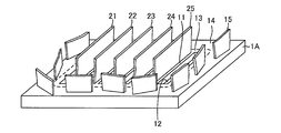
- FIG. 9 is a perspective view showing another silicon substrate in the first embodiment.
- a silicon substrate 1A shown in FIG. 9 may be used.
- silicon substrate 1 ⁇ / b> A is made of the same material as silicon substrate 1 and has regions 13 and 14.
- the region 13 is provided on the inner peripheral side of the region 14 and has the convex portion 11 and the concave portion 12 described above.
- the region 13 is a region where the thin film transistor 10 is formed.
- Region 14 has a flat surface.
- FIG. 10 is a conceptual diagram of a carbon nanowall thin film formed on the silicon substrate 1A shown in FIG.
- a carbon nanowall thin film is formed on silicon substrate 1A using plasma apparatus 100 shown in FIG. 4, a plurality of carbon nanowall thin films 21 to 25 are formed on convex portion 11 in region 13.
- the carbon nanowall thin film 15 is formed in a random direction in the region 14 formed on the convex portion 11 along the length direction (that is, formed with orientation).
- the thin film transistor 10 when the thin film transistor 10 is manufactured in the region 13, if the carbon nanowall thin film 15 exists in the region 14, the electrical characteristics of the thin film transistor 10 may be deteriorated.
- the thin film transistor 10 is manufactured in the region 13
- the carbon nanowall thin film 15 in the region 14 is removed and the thin film transistor 10 is manufactured in the region 13.
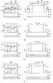
- 11 to 13 are first to third process diagrams showing a method of manufacturing the thin film transistor 10 when the silicon substrate 1A shown in FIG. 9 is used.
- steps (d) to (k) a side view as seen from the length direction of the convex portion 11 and a side view as seen from a direction perpendicular to the length direction of the convex portion 11 are shown.
- steps (a) and (b) shown in FIG. 7 are sequentially performed (steps (a) and ( b)).
- a resist is applied to one main surface of the silicon substrate 30, and the applied resist is patterned by electron beam lithography to form a resist pattern, and the silicon substrate is formed by reactive ion etching using the formed resist pattern as a mask.
- One main surface of the silicon substrate 30 is etched so that a flat portion remains at the peripheral portion of the substrate 30.
- the silicon substrate 1A is placed on the holder 32 in the vacuum vessel 20, and the carbon nanowall thin films 15, 21 to 25 are placed on the silicon substrate 1A under the same conditions as in the step (d) shown in FIG. Form (see step (d)).
- the carbon nanowall thin films 21 to 25 are formed on the convex portion 11 in the region 13 of the silicon substrate 1A, and the carbon nanowall thin film 15 is formed in the region 14 (flat portion) of the silicon substrate 1A.
- a resist is applied on the carbon nanowall thin films 21 to 25 and the region 14 except for both ends in the length direction of the convex portion 11, and the applied resist is patterned by photolithography to form a resist. Patterns 80 and 81 are formed (see step (e)).
- step (e) Ti and Au are sequentially stacked on carbon nanowall thin films 21 to 25 and resist patterns 80 and 81 by electron beam evaporation. Thereby, the source electrode 3 and the drain electrode 4 are formed (see step (f)).
- the metal layer 82 is formed on the resist pattern 80, and the metal layer 83 is formed on the resist pattern 81.
- the resist patterns 80 and 81 are removed using 1-methyl-2-pyrrolidone (see step (g)). Thereby, the metal layers 82 and 83 are removed by lift-off.
- step (h) Ti and Au are sequentially stacked on the insulating film 5 by electron beam evaporation to form the gate electrode 6 (see step (h)).
- a resist is applied so as to cover the region 13, and the applied resist is patterned by photolithography to form a resist pattern 84 (see step (i)).
- gas introducing unit 28 supplies 60 sccm of oxygen (O 2 ) gas into vacuum container 20. And the pressure in the vacuum vessel 20 is adjusted to 4.5 Pa.
- the high frequency power supply 62 applies 100 W high frequency power having a frequency of 13.56 MHz to the planar conductor 50 via the matching circuit 64 and the connection conductor 68.
- plasma 70 is generated in the vacuum chamber 20, and the region 14 of the silicon substrate 1A is treated with oxygen plasma using the resist pattern 84 as a mask (see step (j)).
- the treatment time with oxygen plasma is, for example, 3 minutes.
- step (k) the resist pattern 84 is removed using 1-methyl-2-pyrrolidone.
- the thin film transistor 10 is completed (see step (l)).
- the thin film transistor 10 is formed in the region 13 by removing the carbon nanowall thin film 15 formed in the region 14 using oxygen plasma.
- the carbon nanowall thin film 15 formed on the region 14 is removed by oxygen plasma after the source electrode 3, the drain electrode 4, and the gate electrode 6 are formed.
- the present invention is not limited to this, and after removing the carbon nanowall thin film 15 formed on the region 14, the source electrode 3, the drain electrode 4, and the gate electrode 6 are formed to form the thin film transistor 10. You may make it manufacture.
- FIGS. 14 and 15 are first and second process diagrams showing another method for manufacturing the thin film transistor 10 shown in FIGS. 1 and 2, respectively.
- steps (d), (d-1), (e) to step (h) a side view seen from the length direction of the convex portion 11 and a direction perpendicular to the length direction of the convex portion 11 are used. A side view is shown.
- step 14 and 15 are obtained by adding step (d-1) between step (d) and step (e) in the step diagrams shown in FIGS. 7 and 8.
- the other steps are as follows. This is the same as the process diagram shown in FIGS.
- the gas introduction unit 28 supplies 100 sccm of hydrogen (H 2 ) gas into the vacuum vessel 20. And the pressure in the vacuum vessel 20 is adjusted to 6.65 Pa.
- the high frequency power supply 62 applies 1 kW high frequency power having a frequency of 13.56 MHz to the planar conductor 50 via the matching circuit 64 and the connection conductor 68.
- plasma 70 is generated in the vacuum vessel 20, and the surfaces of the carbon nanowall thin films 21 to 25 are treated with hydrogen plasma (see step (d-1)).
- the processing time by hydrogen plasma is, for example, 1 minute.
- step (d-1) the above-described steps (e) to (h) are sequentially performed to complete the thin film transistor 10 (see steps (e) to (h) in FIG. 15).
- the source electrode 3 and the drain electrode 4 are formed to produce the thin film transistor 10.
- the thin film transistor 10 is manufactured by adding the step (d-1) shown in FIG. 14 between the steps (d) and (e) in the step diagrams shown in FIGS. May be.
- the thin film transistor 10 will be described in detail using examples.
- Example 1 The substrate temperature Ts when forming the carbon nanowall thin films 21 to 25 in the step (d) is set to 400 ° C., and the steps (a) to (h) shown in FIGS. A thin film transistor 10A was produced.
- Example 2 A thin film transistor 10B in Example 2 was produced by the same method as in Example 1 except that the substrate temperature Ts when forming the carbon nanowall thin films 21 to 25 in the step (d) was set to 500 ° C.
- Example 3 A thin film transistor 10C in Example 3 was produced in the same manner as in Example 1 except that the substrate temperature Ts when forming the carbon nanowall thin films 21 to 25 in step (d) was set to 600 ° C.
- Example 4 A thin film transistor 10D according to Example 4 was manufactured using steps (a) to (l) shown in FIGS.
- the substrate temperature Ts when forming the carbon nanowall thin films 21 to 25 is 500 ° C.
- Example 5 A thin film transistor 10E according to Example 5 was manufactured by using the steps (a) to (d), (d-1), and (e) to (h) shown in FIGS.
- the substrate temperature Ts when forming the carbon nanowall thin films 21 to 25 is 600 ° C.
- Example 6 Example 6 7 and 8 except that in step (d), the carbon nanowall thin film was formed by setting the substrate temperature Ts to 400 ° C., and then the carbon nanowall thin film was formed by setting the substrate temperature Ts to 600 ° C.
- the thin film transistor 10F in Example 6 was manufactured using the steps (a) to (h) shown in FIG.
- FIG. 16 is a diagram showing electrical characteristics of the thin film transistor 10A in the first embodiment.
- the vertical axis represents the current I DS flowing between the source electrode 3 and the drain electrode 4
- the horizontal axis represents the voltage V DS applied between the source electrode 3 and the drain electrode 4.
- Curves k1 to k11 show the current I DS and the voltage V DS when the gate voltage is 5, 4, 3, 2, 1, 0, -1, -2, -3, -4, -5 V, respectively. Shows the relationship.
- the current I DS increases as the gate voltage changes from +5 V to ⁇ 5 V at the same voltage value of the voltage V DS (see curves k1 to k11).
- the carbon nanowall thin films 21 to 25 formed at a substrate temperature Ts of 400 ° C. have semiconductor characteristics and can be used as a channel layer of a thin film transistor.
- FIG. 17 is a diagram illustrating the electrical characteristics of the thin film transistor 10B in the second embodiment.
- the vertical axis represents the current I DS flowing between the source electrode 3 and the drain electrode 4
- the horizontal axis represents the voltage V DS applied between the source electrode 3 and the drain electrode 4.
- Curves k12 to k22 show current I DS and voltage V DS when the gate voltage is 5, 4, 3, 2, 1, 0, -1, -2, -3, -4, -5 V, respectively. Shows the relationship.
- the current-voltage characteristic I DS -V DS is inferior to the current-voltage characteristic I DS -V DS shown in FIG. 16, the current I DS has a voltage V DS of ⁇ 1 V at each gate voltage. Increases from 1 to +1 V (see curves k12 to k22).
- the current I DS increases as the gate voltage changes from +5 V to ⁇ 5 V at the same voltage value of the voltage V DS (see curves k12 to k22).
- the carbon nanowall thin films 21 to 25 formed at a substrate temperature Ts of 500 ° C. also have semiconductor characteristics and can be used as a channel layer of a thin film transistor.
- the thin film transistor 10C in Example 3 in which the substrate temperature Ts when forming the carbon nanowall thin films 21 to 25 is 600 ° C. has the same electrical characteristics as the thin film transistors 10A and 10B.
- the substrate temperature Ts becomes 600 ° C. higher than 400 ° C. and 500 ° C.
- the crystallinity of the carbon nanowall thin films 21 to 25 is improved. Therefore, the carbon nanowall thin films 21 to 25 formed using the substrate temperature Ts of 600 ° C. This is because it is considered to have semiconductor characteristics.
- the carbon nanowall thin films 21 to 25 are formed using the substrate temperature Ts in the range of 400 ° C. to 600 ° C.
- FIG. 18 is a diagram illustrating electrical characteristics of the thin film transistor 10D in the fourth embodiment.
- the vertical axis represents the current I DS flowing between the source electrode 3 and the drain electrode 4
- the horizontal axis represents the voltage V DS applied between the source electrode 3 and the drain electrode 4.
- the gate voltage is + 5V to ⁇ 5V.
- current I DS increases exponentially when voltage V DS is 0 V or higher or when voltage V DS is 0.5 V or higher.
- the substrate temperature Ts when forming the carbon nanowall thin films 21 to 25 is 500 ° C., and the carbon formed in the region 14 other than the region 13 where the thin film transistor 10 is formed after the carbon nanowall thin films 21 to 25 are formed.
- the current-voltage characteristic I DS -V DS of the thin film transistor becomes the current-voltage characteristic I DS -V DS shown in FIG.
- the thin film transistor 10D in Example 4 was manufactured by forming the carbon nanowall thin films 21 to 25 using a substrate temperature Ts of 500 ° C., and removing the carbon nanowall thin film formed in the region 14 by oxygen plasma. .
- the thin film transistor 10D has a current-voltage characteristic I DS -V DS that is superior to the current-voltage characteristic I DS -V DS shown in FIG.
- the leakage current of the thin film transistor is 10 ⁇ A, whereas the carbon nanowall thin film formed in the region 14 is used using oxygen plasma. When removed, the leakage current of the thin film transistor is 100 pA.
- the leakage current can be greatly reduced, and as a result, the current-voltage characteristics I DS -V DS can be greatly improved.
- FIG. 19 is a view showing a SEM (Scanning Electron Microscope) photograph of a region where a thin film transistor electrode (source electrode or drain electrode) is formed.
- FIG. 19 (a) shows an SEM photograph when the carbon nanowall thin film is not treated with hydrogen plasma
- FIG. 19 (b) shows an SEM photograph when the carbon nanowall thin film is treated with hydrogen plasma.
- the electrode is formed in a film shape and is placed on the carbon nanowall thin film (see FIG. 19A).
- the electrode is formed following the carbon nanowall thin film that is the base, and the adhesion between the electrode and the carbon nanowall thin film can be increased (FIG. 19). (See (b)).
- the thin film transistor 10E of Example 5 the adhesion between the source electrode 3 and the drain electrode 4 and the carbon nanowall thin films 21 to 25 can be increased. As a result, the thin film transistor 10E is considered to have good current-voltage characteristics I DS -V DS .
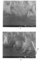
- FIG. 20 is a view showing a cross-sectional SEM photograph of the carbon nanowall thin film.
- 20A shows a cross-sectional SEM photograph of a carbon nanowall thin film formed using a substrate temperature Ts of 600 ° C.
- FIG. 20B shows a carbon nanowall using a substrate temperature Ts of 400 ° C.
- a cross-sectional SEM photograph of a carbon nanowall thin film formed by forming a thin film and then raising the substrate temperature Ts to 600 ° C. is shown.
- the carbon nanowall thin film is formed using the substrate temperature Ts of 600 ° C., the carbon nanowall thin film is uniformly grown from the substrate (see FIG. 20A).
- the carbon nanowall thin film grown at a substrate temperature Ts of 400 ° C. has semiconductor characteristics as shown in FIG. 16, and the growth rate of the carbon nanowall thin film increases when the substrate temperature Ts is increased from 400 ° C. to 600 ° C. Therefore, the carbon nanowall thin film having semiconductor characteristics can be formed in a short time by switching the substrate temperature Ts to two stages of 400 ° C. and 600 ° C. As a result, surplus carbides can be reduced, and damage to the carbon nanowall thin film due to etching can be reduced.
- the thin film transistor 10F of Example 6 is considered to have good current-voltage characteristics I DS -V DS .
- the thin film transistors 10A, 10B, 10C, 10D, 10E, and 10F in Examples 1 to 6 have a structure in which a plurality of carbon nanowall thin films 21 to 25 are arranged in parallel between the source electrode 3 and the drain electrode 4. And has a good current-voltage characteristic I DS -V DS .
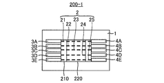
- FIG. 21 is a plan view showing the configuration of another thin film transistor according to the first embodiment.
- the thin film transistor according to the first embodiment may be the thin film transistor 10-1 shown in FIG.
- thin film transistor 10-1 is obtained by replacing source electrode 3 of thin film transistor 10 shown in FIGS. 1 and 2 with source electrodes 3A to 3E and drain electrode 4 with drain electrodes 4A to 4E.
- the others are the same as those of the thin film transistor 10.
- the source electrodes 3A to 3E are provided corresponding to the carbon nanowall thin films 21 to 25, respectively, and are connected to one end of the carbon nanowall thin films 21 to 25 in the length direction of the convex portion 11 of the silicon substrate 1. .
- the drain electrodes 4A to 4E are provided corresponding to the carbon nanowall thin films 21 to 25, respectively, and are connected to the other ends of the carbon nanowall thin films 21 to 25 in the length direction of the convex portions 11 of the silicon substrate 1. .
- the thin film transistor 10-1 has the same cross-sectional structure as the thin film transistor 10 shown in FIG. 1, in the thin film transistor 10-1, the insulating film 5 and the gate electrode 6 are formed to face the entire surface of the channel layer 2. ing.
- the carbon nanowall thin film 21, the source electrode 3A, the drain electrode 4A, the insulating film 5 and the gate electrode 6 constitute one thin film transistor
- the carbon nanowall thin film 22 constitute one thin film transistor
- the source electrode 3B, the drain The electrode 4B, the insulating film 5 and the gate electrode 6 constitute one thin film transistor
- the carbon nanowall thin film 23 constitute one thin film transistor
- the nanowall thin film 24, the source electrode 3D, the drain electrode 4D, the insulating film 5 and the gate electrode 6 constitute one thin film transistor.
- the carbon nanowall thin film 25, the source electrode 3E, the drain electrode 4E, the insulating film 5 and the gate electrode 6 are included. Is one thin film transistor To configure.
- the thin film transistor 10-1 has a configuration in which five thin film transistors are arranged in parallel in the in-plane direction of the silicon substrate 1.
- the thin film transistor 10-1 is obtained by etching a part of the source electrode 3 and the drain electrode 4 between the step (g) and the step (h) in the process diagrams shown in FIGS. , 3C, 3D, 3E and the process of forming the drain electrodes 4A, 4B, 4C, 4D, 4E are manufactured according to a process diagram.
- the source electrode 3A is etched by etching a part of the source electrode 3 and the drain electrode 4 between the step (g) and the step (h) in the process charts shown in FIGS. , 3B, 3C, 3D, 3E and the process of forming the drain electrodes 4A, 4B, 4C, 4D, 4E may be manufactured according to a process diagram.
- the thin film transistor 10-1 is obtained by etching a part of the source electrode 3 and the drain electrode 4 between the step (g) and the step (h) in the step diagrams shown in FIGS. , 3B, 3C, 3D, 3E and the process of forming the drain electrodes 4A, 4B, 4C, 4D, 4E may be manufactured according to a process diagram.
- the channel layer 2 It is possible to control the current value flowing in the step by step.
- the gate electrode 6 may be composed of five gate electrodes corresponding to the five carbon nanowall thin films 21 to 25.
- the five gate electrodes are formed at positions facing the five carbon nanowall thin films 21 to 25, respectively.
- the current value flowing through each of the carbon nanowall thin films 21 to 25 can be independently controlled by the gate voltage applied to the gate electrode.
- a step of dividing the formed gate electrode 6 into five gate electrodes by etching is added, or the gate electrode 6 is formed on the entire back surface of the silicon substrate 1 (or silicon substrate 1A). Instead of this step, a step of forming five gate electrodes using a mask may be employed.
- the other description of the thin film transistor 10-1 is the same as the description of the thin film transistor 10.
- the height of the carbon nanowall thin films 21 to 25 is the channel width. Therefore, in the thin film transistors 10 and 10-1, the channel width can be controlled by controlling the height of the carbon nanowall thin films 21 to 25.
- the thin film transistors 10 and 10-1 include the five carbon nanowall thin films 21 to 25.
- the thin film transistors 10 and 10-1 are not limited to this. Specifically, it is only necessary to have two or more carbon nanowall thin films.
- the thin film transistor 10-1 may include the same number of source electrodes and drain electrodes as the number of carbon nanowall thin films, and is the same as the number of carbon nanowall thin films. A number of source electrodes, drain electrodes, and gate electrodes may be provided.
- the silicon substrates 1 and 1A may have a concavo-convex shape formed in a grid pattern on one main surface, and generally, a concavo-convex shape formed in a stripe pattern or a grid pattern on a main surface. You should be prepared for. This is because a plurality of carbon nanowall thin films can be formed in parallel on the silicon substrate even if the concavo-convex shape formed in a grid pattern is formed.
- FIG. 22 is a cross-sectional view showing the structure of the thin film transistor according to the second embodiment.
- FIG. 23 is a plan view of the thin film transistor viewed from the direction A shown in FIG.
- thin film transistor 200 according to the second embodiment is obtained by replacing insulating film 5 of thin film transistor 10 shown in FIGS. 1 and 2 with insulating film 210 and replacing gate electrode 6 with gate electrode 220. Others are the same as those of the thin film transistor 10.
- the insulating film 210 is generally made of a dielectric, and is disposed on the carbon nanowall thin films 21 to 25 in contact with the carbon nanowall thin films 21 to 25.
- the dielectric is made of, for example, silicon oxide, barium titanate and ionic liquid.
- the gate electrode 220 is made of the same material as the gate electrode 6 described above, and is disposed on the insulating film 210 in contact with the insulating film 210.
- the thin film transistor 200 is a top gate type thin film transistor in which the gate electrode 220 is disposed above the channel layer 2.
- 24 to 26 are first to third process diagrams showing a method of manufacturing the thin film transistor 200 shown in FIGS. 22 and 23, respectively.
- steps (c) to (k) a side view seen from the length direction of the convex portion 11 and a side view seen from a direction perpendicular to the length direction of the convex portion 11 are shown.
- steps (e) to (k) the carbon nanowall thin films 21 to 25 covered with the source electrode 3 are indicated by dotted lines.
- steps (d) and (e) shown in FIG. 7 and steps (f) and (g) shown in FIG. 8 are sequentially executed (steps (c) to (e) and FIG. 24 shown in FIG. 24). Step (f) shown in FIG. 25).
- step (f) a resist is applied on source electrode 3, drain electrode 4 and carbon nanowall thin films 21 to 25, and the applied resist is patterned by photolithography and etching.
- a resist pattern 201 is formed (see step (g)).
- an insulating film 210 is formed on the carbon nanowall thin films 21 to 25 using the resist pattern 201 as a mask (see step (h)).
- the insulating film 202 is formed on the resist pattern 201.
- step (h) resist pattern 201 is removed (see step (i)). Thereby, the insulating film 202 is removed by lift-off.
- a resist is applied on the source electrode 3, the drain electrode 4, and the insulating film 210, and the applied resist is patterned by photolithography and etching to form a resist pattern 203 (see step (j)).
- step (k) Thereafter, Ti and Au are sequentially stacked on the insulating film 210 by electron beam evaporation, and the resist pattern 203 is removed. Thus, the gate electrode 220 is formed on the insulating film 210, and the thin film transistor 200 is completed (see step (k)).
- FIGS. 1 to 4 are process diagrams of FIGS. 1 to 4 showing another method for manufacturing the thin film transistor 200 shown in FIGS. 22 and 23, respectively.
- steps (c) to (n) a side view seen from the length direction of the convex portion 11 and a side view seen from a direction perpendicular to the length direction of the convex portion 11 are shown.
- steps (h) to (n) the carbon nanowall thin films 21 to 25 covered with the source electrode 3 are indicated by dotted lines.
- step (a) when the manufacture of thin film transistor 200 is started, the same step as step (a) shown in FIG. 11 is performed (see step (a)).
- steps (c) and (d) shown in FIG. 11 are sequentially performed (see step (b) and step (c) in FIG. 27).
- step (c) After the step (c), a resist is applied so as to cover the region 13, and the applied resist is patterned by photolithography to form a resist pattern 85 (see step (d)).
- the gas introduction unit 28 supplies 60 sccm of O 2 gas into the vacuum container 20. And the pressure in the vacuum vessel 20 is adjusted to 4.5 Pa.
- the high frequency power supply 62 applies 100 W high frequency power having a frequency of 13.56 MHz to the planar conductor 50 via the matching circuit 64 and the connection conductor 68.
- the treatment time with oxygen plasma is, for example, 3 minutes.
- the carbon nanowall thin film 15 is removed.
- the resist pattern 85 is removed using 1-methyl-2-pyrrolidone (see step (f) in FIG. 28).
- a resist is applied on the carbon nanowall thin films 21 to 25 except for both ends in the length direction of the convex portion 11, and the applied resist is patterned by photolithography to form a resist pattern 86 (step ( g)).
- the resist pattern 86 is removed using 1-methyl-2-pyrrolidone (see step (i)). Thereby, the metal layer 87 is removed by lift-off.
- step (i) a resist is applied on source electrode 3, drain electrode 4 and carbon nanowall thin films 21-25, and the applied resist is patterned by photolithography and etching, A resist pattern 204 is formed (see step (j)).
- an insulating film 210 is formed on the carbon nanowall thin films 21 to 25 using the resist pattern 204 as a mask (see step (k)).
- the insulating film 205 is formed on the resist pattern 204.
- step (l) the resist pattern 204 is removed (see step (l)). Thereby, the insulating film 205 is removed by lift-off.
- step (l) a resist is applied on source electrode 3, drain electrode 4 and insulating film 210, and the applied resist is patterned by photolithography and etching to form resist pattern 206. Form (see step (m)).
- step (n) Thereafter, Ti and Au are sequentially stacked on the insulating film 210 by electron beam evaporation, and the resist pattern 206 is removed. Thus, the gate electrode 220 is formed on the insulating film 210, and the thin film transistor 200 is completed (see step (n)).
- the thin film transistor 200 is manufactured by removing the carbon nanowall thin film 15 formed in the region 14 by oxygen plasma. As a result, leakage current can be significantly reduced in the top-gate thin film transistor 200.
- the thin film transistor 200 is formed by forming the source electrode 3, the drain electrode 4 and the gate electrode 220 after removing the carbon nanowall thin film 15 formed on the region 14 by oxygen plasma.
- the carbon nanowall thin film 15 formed on the region 14 is formed after the source electrode 3, the drain electrode 4 and the gate electrode 220 are formed.
- the thin film transistor 200 may be manufactured by removing with oxygen plasma.
- FIGS. 31 to 33 are process diagrams of FIGS. 1 to 3 showing still another method of manufacturing the thin film transistor 200 shown in FIGS. 22 and 23, respectively.
- steps (c) to (k) a side view seen from the length direction of the convex portion 11 and a side view seen from a direction perpendicular to the length direction of the convex portion 11 are shown.
- steps (e) to (k) the carbon nanowall thin films 21 to 25 covered with the source electrode 3 are indicated by dotted lines.
- FIGS. 31 to 33 are obtained by adding a process (d-1) between the process (d) and the process (e) in the process diagrams shown in FIGS. This is the same as the process diagram shown in FIGS.
- steps (a) to (d) described in FIG. 24 are sequentially performed (see steps (a) to (d). ).
- step (d) the same step as step (d-1) shown in FIG. 14 is executed (see step (d-1)).
- step (e) shown in FIG. 24, step (f) to step (h) shown in FIG. 25, and step (i) to step (k) shown in FIG. See step (e) to step (h) shown in FIG. 32 and step (i) to step (k) shown in FIG. 33).
- the source electrode 3 and the drain electrode 4 are formed to manufacture the thin film transistor 200.
- the adhesion between the source electrode 3 and the drain electrode 4 can be improved.
- the thin film transistor 200 according to the second embodiment is a process diagram that does not use both oxygen plasma treatment and hydrogen plasma treatment (step diagrams shown in FIGS. 24 to 26), and a process diagram that uses oxygen plasma treatment (FIG. It may be manufactured according to any of the process diagrams (process diagrams shown in FIGS. 27 to 30) and process diagrams using hydrogen plasma treatment (process diagrams shown in FIGS. 31 to 33).
- the thin film transistor 200 is manufactured by adding the step (d-1) of FIG. 31 between the step (f) and the step (g) of the step diagrams shown in FIGS. May be. Accordingly, in the top gate type thin film transistor 200, the leakage current can be greatly reduced and the adhesion between the source electrode 3 and the drain electrode 4 can be improved.
- FIG. 34 is a plan view showing the configuration of another thin film transistor according to the second embodiment.
- the thin film transistor according to the second embodiment may be a thin film transistor 200-1 shown in FIG.
- thin film transistor 200-1 is obtained by replacing source electrode 3 of thin film transistor 200 shown in FIGS. 22 and 23 with source electrodes 3A to 3E and replacing drain electrode 4 with drain electrodes 4A to 4E.
- the others are the same as those of the thin film transistor 200.
- the source electrodes 3A to 3E and the drain electrodes 4A to 4E are as described above.
- the thin film transistor 200-1 has a configuration in which five thin film transistors are arranged in parallel in the in-plane direction of the silicon substrate 1, similarly to the thin film transistor 10-1 (see FIG. 21).
- the thin film transistor 200-1 is formed by etching a part of the source electrode 3 and the drain electrode 4 between the steps (f) and (g) in the step diagrams shown in FIGS. , 3C, 3D, 3E and the process of forming the drain electrodes 4A, 4B, 4C, 4D, 4E are manufactured according to a process diagram.
- the thin film transistor 200-1 is formed by etching a part of the source electrode 3 and the drain electrode 4 between the step (i) and the step (j) in the step diagrams shown in FIGS. , 3B, 3C, 3D, 3E and the process of forming the drain electrodes 4A, 4B, 4C, 4D, 4E may be manufactured according to a process diagram.
- the thin film transistor 200-1 is formed by etching a part of the source electrode 3 and the drain electrode 4 between the step (f) and the step (g) in the step diagrams shown in FIGS. , 3B, 3C, 3D, 3E and the process of forming the drain electrodes 4A, 4B, 4C, 4D, 4E may be manufactured according to a process diagram.
- the thin film transistor 200-1 is different from the thin film transistor 10-1 only in that the insulating film 210 and the gate electrode 220 are disposed on the upper side of the channel layer 2, so that the same effect as the thin film transistor 10-1 can be enjoyed.
- the other description of the thin film transistor 200-1 is the same as the description of the thin film transistor 10-1.
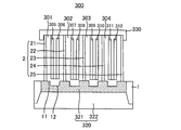
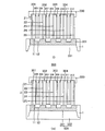
- FIG. 35 is a sectional view showing the structure of the thin film transistor according to the third embodiment.
- thin film transistor 300 according to the third embodiment includes silicon substrate 1, channel layer 2, insulating films 301-304, gate electrodes 305-312, source electrode 320, and drain electrode 330. Prepare.
- the silicon substrate 1 and the channel layer 2 are as described above.
- the source electrode 320 is disposed on one main surface side of the silicon substrate 1.
- the source electrode 320 includes an impurity region 321 and a metal region 322.
- Impurity region 321 is in contact with convex portion 11 and concave portion 12 of silicon substrate 1 and is arranged in silicon substrate 1.
- Impurity region 321 has the same conductivity type as that of silicon substrate 1 or an opposite conductivity type, and has an impurity concentration of about 10 20 cm ⁇ 3 . More specifically, the impurity region 321 has a phosphorus (P) concentration or boron (B) concentration of about 10 20 cm ⁇ 3 regardless of the conductivity type of the silicon substrate 1.
- the metal region 322 is disposed in contact with the silicon substrate 1 and the impurity region 321.
- the metal region 322 has a structure in which Ti and Au are sequentially stacked.
- one end of the carbon nanowall thin films 21 to 25 is connected to the source electrode 320.
- the insulating films 301 to 304 are arranged between the carbon nanowall thin films 21 and 22, between the carbon nanowall thin films 22 and 23, between the carbon nanowall thin films 23 and 24, and between the carbon nanowall thin films 24 and 25, respectively. It has a U-shaped cross-sectional shape.
- Each of the insulating films 301 to 304 is made of, for example, SiO 2 .
- the insulating film 301 is in contact with the carbon nanowall thin films 21 and 22 and the source electrode 320.
- the insulating film 302 is in contact with the carbon nanowall thin films 22 and 23 and the source electrode 320.
- the insulating film 303 is in contact with the carbon nanowall thin films 23 and 24 and the source electrode 320.
- the insulating film 304 is in contact with the carbon nanowall thin films 24 and 25 and the source electrode 320.
- the gate electrode 305 is disposed opposite to the carbon nanowall thin film 21 and in contact with the insulating film 301.
- the gate electrode 306 is disposed opposite to one surface of the carbon nanowall thin film 22 and in contact with the insulating film 301.
- the gate electrode 307 is disposed opposite to the other surface of the carbon nanowall thin film 22 and in contact with the insulating film 302.
- the gate electrode 308 is disposed opposite to one surface of the carbon nanowall thin film 23 and in contact with the insulating film 302.
- the gate electrode 309 is disposed opposite to the other surface of the carbon nanowall thin film 23 and in contact with the insulating film 303.
- the gate electrode 310 is disposed opposite to one surface of the carbon nanowall thin film 24 and in contact with the insulating film 303.
- the gate electrode 311 is disposed opposite to the other surface of the carbon nanowall thin film 24 and in contact with the insulating film 304.
- the gate electrode 312 faces the one surface of the carbon nanowall thin film 25 and is disposed in contact with the insulating film 304.
- the drain electrode 330 is disposed in contact with the carbon nanowall thin films 21 to 25 and the insulating films 301 to 304. More specifically, the drain electrode 330 is in contact with the side surface parallel to the thickness direction of the carbon nanowall thin films 21 to 25 and the side surface parallel to the thickness direction of the insulating films 301 to 304 on the side opposite to the silicon substrate 1 side. Be placed.
- Each of the gate electrodes 305 to 312 and the drain electrode 330 has a structure in which Ti and Au are sequentially stacked.
- the thin film transistor 300 when a desired voltage is applied to the gate electrodes 305, 307, 309, 311, and 312 and a desired voltage is applied between the source electrode 320 and the drain electrode 330, the current is reduced to the carbon nanowall thin film. 21 to 25 flow in the normal direction of the silicon substrate 1. The current flowing through the carbon nanowall thin films 21 to 25 is controlled by the voltage applied to the gate electrodes 305, 307, 309, 311 and 312.
- a desired voltage may be applied to the gate electrodes 306, 308, 310 instead of the gate electrodes 307, 309, 311.
- the gate electrodes 306, 307; 309; 310, 311 may be applied with a desired voltage.
- the channel layer 2 has a structure in which five carbon nanowall thin films 21 to 25 are arranged in parallel between the source electrode 320 and the drain electrode 330 in the normal direction of the silicon substrate 1. As a result, a current flows in parallel between the source electrode 320 and the drain electrode 330.
- the channel layer 2 is disposed in the normal direction of the silicon substrate 1, the degree of integration of the thin film transistors 300 can be increased as compared with the case where the channel layer is disposed in the in-plane direction of the silicon substrate 1.
- the channel width is determined by the dimensions of the carbon nanowall thin films 21 to 25 in the length direction of the convex portion 11 (the direction perpendicular to the paper surface of FIG. 35), and the carbon nanowall thin films 21 to 25 are formed on the convex portion 11. Therefore, the channel width can be controlled by the length of the convex portion 11.
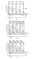
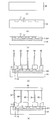
- 36 to 39 are first to fourth process diagrams showing a method of manufacturing the thin film transistor 300 shown in FIG. 35, respectively.
- steps (a) and (c) shown in FIG. 7 are sequentially performed to manufacture silicon substrate 1 (steps (a) and ( b)).
- impurity atoms (P or B) are ion-implanted into one main surface of the silicon substrate 1 where the convex portions 11 and the concave portions 12 are formed, thereby forming an impurity region 321 (see step (c)). ).
- an insulating film 340 made of SiO 2 is formed on the silicon substrate 1 between the carbon nanowall thin films 21 to 25 (see step (e)).
- the insulating film 340 is formed by plasma CVD using, for example, silane (SiH 4 ) gas and O 2 gas as material gases.
- a resist is applied onto carbon nanowall thin films 21 to 25 and insulating film 340, and the applied resist is patterned by photolithography and etching to form resist pattern 341. Form (see step (f)).
- the insulating film 340 is etched using the resist pattern 341 as a mask to form insulating films 301 to 304 (see step (g)).
- Ti and Au are sequentially deposited so as to be in contact with the insulating films 301 to 304 by electron beam evaporation using the resist pattern 341 as a mask to form metal layers 342 to 345, and the resist pattern 341 is removed (see step (h)). ).
- the metal layer deposited on the resist pattern 341 is removed by lift-off.
- a resist is applied on carbon nanowall thin films 21-25, insulating films 301-304, and metal layers 342-345, and the applied resist is subjected to photolithography and etching. Patterning is performed to form a resist pattern 350 (see step (i)).
- gate electrodes 305 to 3112 are formed.
- step (k) the back surface side of silicon substrate 1 is etched to form recess 351 reaching impurity region 321 (see step (l)).
- step (m) Ti and Au are sequentially deposited in the recess 351 by electron beam evaporation to form a metal region 322.
- the source electrode 320 is formed, and the thin film transistor 300 is completed (see step (m)).
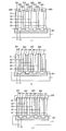
- 40 to 44 are first to fifth process diagrams showing another method for manufacturing the thin film transistor 300 shown in FIG. 35, respectively.
- steps (a) and (b) shown in FIG. 27 are sequentially performed to manufacture silicon substrate 1A (steps (a) and ( b)).
- step (b) impurity atoms (P or B) are ion-implanted into one main surface of the silicon substrate 1A where the convex portions 11 and the concave portions 12 are formed, thereby forming an impurity region 321 (step (c) )reference).
- steps (c) to (e) shown in FIG. 27 and the step (f) shown in FIG. 28 are sequentially executed, and the carbon nanowall thin films 15 other than the carbon nanowall thin films 21 to 25 are formed by oxygen plasma.
- the resist pattern 85 is removed (see steps (d) and (e) in FIG. 40 and steps (f) and (g) in FIG. 41).
- step (g) the same steps as step (e) in FIG. 36 to step (m) in FIG. 39 are sequentially performed (step (h) in FIG. 41, steps (i) to steps in FIG. 42). (K), see steps (l) to (n) in FIG. 43 and steps (o) and (p) in FIG. 44). Thereby, the thin film transistor 300 is completed.
- the thin film transistor 300 in which the channel layer 2 is arranged in the normal direction of the silicon substrate 1A is also manufactured by removing the carbon nanowall thin film 15 formed in the region 14 with oxygen plasma. As a result, leakage current can be significantly reduced in the thin film transistor 300.
- the carbon nanowall thin film 15 formed on the region 14 is removed by oxygen plasma, and then the gate electrodes 305 to 312, the source electrode 320 and the drain electrode 330 are formed.
- the present invention is not limited to this, and after forming the gate electrodes 305 to 312, the source electrode 320, and the drain electrode 330, the carbon nano-particles formed on the region 14 are formed.
- the thin film 300 may be manufactured by removing the wall thin film 15 with oxygen plasma.
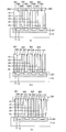
- 45 to 48 are first to fourth process diagrams showing still another method for manufacturing the thin film transistor 300 shown in FIG. 35, respectively.
- FIGS. 45 to 48 are obtained by adding a process (d-1) between the process (d) and the process (e) in the process diagrams shown in FIGS. 36 to 39. This is the same as the process diagram shown in FIGS.
- steps (a) to (d) shown in FIG. 36 are sequentially performed (see steps (a) to (d)). .
- step (e) to step (m) in FIG. 36 are sequentially performed (step (e) to step (g) in FIG. 46, step (h) to step in FIG. 47). (J) and steps (k) to (m) in FIG. 48). Thereby, the thin film transistor 300 is completed.
- the thin film transistor 300 in which the channel layer 2 is arranged in the normal direction of the silicon substrate 1A is also manufactured by forming the drain electrode 330 after treating the surfaces of the carbon nanowall thin films 21 to 25 with hydrogen plasma. As a result, in the thin film transistor 300, the adhesion of the drain electrode 330 can be improved.
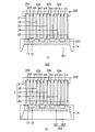
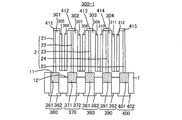
- FIG. 49 is a cross-sectional view showing the configuration of another thin film transistor according to the third embodiment.
- the thin film transistor according to the third embodiment may be a thin film transistor 300-1 shown in FIG.
- source electrode 320 of thin film transistor 300 shown in FIG. 35 is replaced with source electrodes 360, 370, 380, 390, and 400, and drain electrode 330 is replaced with drain electrodes 411 to 415.
- the others are the same as those of the thin film transistor 300.
- Source electrodes 360, 370, 380, 390, and 400 are provided corresponding to the carbon nanowall thin films 21 to 25, respectively.
- the source electrode 360 includes an impurity region 361 and a metal region 362.
- Source electrode 370 includes an impurity region 371 and a metal region 372.
- Source electrode 380 includes an impurity region 381 and a metal region 382.
- Source electrode 390 includes an impurity region 391 and a metal region 392.
- Source electrode 400 includes an impurity region 401 and a metal region 402.
- Each of the impurity regions 361, 371, 381, 391, 401 is disposed in the silicon substrate 1 in contact with the convex portion 11 of the silicon substrate 1.
- Each of impurity regions 361, 371, 381, 391, 401 has the same conductivity type as that of silicon substrate 1 or an opposite conductivity type, and has an impurity concentration of about 10 20 cm ⁇ 3 . More specifically, each of the impurity regions 361, 371, 381, 391, 401 has a P concentration or a B concentration of about 10 20 cm ⁇ 3 regardless of the conductivity type of the silicon substrate 1.
- the metal regions 362, 372, 382, 392, 402 are in contact with the impurity regions 361, 371, 381, 391, 401 and the silicon substrate 1, respectively.
- Each of the metal regions 362, 372, 382, 392, 402 has a structure in which Ti and Au are sequentially laminated.
- each of the impurity regions 361, 371, 381, 391, 401 being disposed in the silicon substrate 1 in contact with the convex portion 11 of the silicon substrate 1, the carbon nanowall thin films 21 to 25 in the normal direction of the silicon substrate 1 are arranged.
- One end is in contact with the source electrodes 360, 370, 380, 390, and 400, respectively.
- Each of the drain electrodes 411 to 415 has a structure in which Ti and Au are sequentially laminated.
- the drain electrodes 411 to 415 are arranged in contact with the side surfaces parallel to the thickness direction of the carbon nanowall thin films 21 to 25 and the side surfaces parallel to the thickness direction of the insulating films 301 to 304 on the side opposite to the silicon substrate 1 side, respectively. Is done.
- the carbon nanowall thin film 21, the source electrode 360, the drain electrode 411, the insulating film 301, and the gate electrode 305 constitute one thin film transistor.
- the carbon nanowall thin film 22, the source electrode 370, and the drain electrode 412 The insulating films 301 and 302 and the gate electrodes 306 and 307 constitute one thin film transistor, and the carbon nanowall thin film 23, the source electrode 380, the drain electrode 413, the insulating films 302 and 303, and the gate electrodes 308 and 309 are one.
- a thin film transistor is formed, and the carbon nanowall thin film 24, the source electrode 390, the drain electrode 414, the insulating films 303 and 304, and the gate electrodes 310 and 311 form one thin film transistor, and the carbon nanowall thin film 2 , Source electrode 400, drain electrode 415, the insulating film 304 and the gate electrode 312 constitute one thin film transistor.
- the thin film transistor 300-1 has a configuration in which five thin film transistors are arranged in parallel in the normal direction of the silicon substrate 1.
- impurity atoms P or B
- drain electrodes 411 to 415 are formed in step (c) of the process charts shown in FIGS. 391, 401, and in step (k), drain electrodes 411 to 415 are formed.
- step (l) five holes respectively contacting the impurity regions 361, 371, 381, 391, 401 are formed on the silicon substrate. 1 is manufactured by forming metal regions 362, 372, 382, 392, and 402 in the formed five holes in the step (m), respectively.
- impurity atoms (P or B) are ion-implanted only into the convex portion 11 of the silicon substrate 1A in the step (c) of the process charts shown in FIGS. , 381, 391, 401, and in step (n), drain electrodes 411 to 415 are formed.
- step (o) five holes respectively contacting the impurity regions 361, 371, 381, 391, 401 are formed. It may be manufactured by forming it on the back side of the silicon substrate 1 and forming metal regions 362, 372, 382, 392, 402 in the formed five holes in the step (p), respectively.
- impurity atoms (P or B) are ion-implanted only into the convex portion 11 of the silicon substrate 1 in step (c) of the process charts shown in FIGS. , 381, 391, 401, and in step (k), drain electrodes 411 to 415 are formed.
- step (l) five holes respectively contacting the impurity regions 361, 371, 381, 391, 401 are formed. It may be formed by forming the metal region 362, 372, 382, 392, 402 in the formed five holes in the step (m).
- the thin film transistor 300-1 has a configuration in which five thin film transistors are arranged in parallel in the normal direction of the silicon substrate 1, the same effect as the above-described thin film transistor 10-1 (see FIG. 21) can be obtained.
- the drain electrode 330 is arranged in the silicon substrate 1 like the source electrode 320, and the source electrode 320 is carbon on the opposite side to the silicon substrate 1 side in the normal direction of the silicon substrate 1 like the drain electrode 330. It may be in contact with the nanowall thin films 21-25.
- either the source electrode 320 or the drain electrode 330 is disposed in the silicon substrate 1 so as to be in contact with the convex portion 11 and the concave portion 12, and either the source electrode 320 or the drain electrode 330 is the other electrode. What is necessary is just to contact the carbon nanowall thin films 21 to 25 on the opposite side to the silicon substrate 1 side in the normal direction of the silicon substrate 1.
- the thin film transistor 300-1 is also disposed in the silicon substrate 1 so that any one of the source electrodes 360, 370, 380, 390, 400 and the drain electrodes 411 to 415 is in contact with the convex portion 11, and the source electrodes 360, 370, Any one of 380, 390, 400 and the drain electrodes 411 to 415 may be in contact with the carbon nanowall thin films 21 to 25 on the side opposite to the silicon substrate 1 side in the normal direction of the silicon substrate 1.
- the back-gate thin film transistors 10 and 10-1 will be described, and in the second embodiment, the top-gate thin film transistors 200 and 200-1 will be described.
- the thin film transistors 300 and 300-1 in which the channel layer 2 is arranged in the normal direction of the silicon substrates 1 and 1A have been described.
- the thin film transistor according to the embodiment of the present invention includes a silicon substrate having a concavo-convex shape formed in a stripe shape or a grid pattern on one main surface, and a plurality of convex portions along the length direction of the concavo-convex convex portion.
- a channel layer composed of a plurality of carbon nanowall thin films each grown in the normal direction of the silicon substrate, and a first side surface parallel to the thickness direction of the carbon nanowall thin film in each of the plurality of carbon nanowall thin films
- a drain electrode that is disposed so as to face the source electrode in the in-plane direction of the carbon nanowall thin film and that is at least in contact with the second side face that faces the first side face in each of the plurality of carbon nanowall thin films Insulation disposed between the electrode, the gate electrode, the plurality of carbon nanowall thin films and the gate electrode Door or if it has a.
- a thin film transistor manufacturing method is a method of manufacturing a thin film transistor using a plurality of carbon nanowall thin films as channel layers, wherein the concavo-convex shape is striped or cross-cut on one main surface of the silicon substrate.
- a first step of forming a plurality of carbon nanowall thin films on a plurality of convex portions along a length direction of the convex portions having a concavo-convex shape, and a plurality of carbon nanowall thin films A third step of forming a source electrode so as to be at least in contact with a first side surface parallel to the thickness direction of the carbon nanowall thin film, and a source electrode in the in-plane direction of the carbon nanowall thin film.
- Each of the plurality of carbon nanowall thin films so as to be at least in contact with the second side surface opposite to the first side surface
- the present invention is applied to a thin film transistor and a manufacturing method thereof.
Landscapes
- Thin Film Transistor (AREA)
- Electrodes Of Semiconductors (AREA)
Abstract
Description
図1は、この発明の実施の形態1による薄膜トランジスタの構成を示す断面図である。また、図2は、図1に示すA方向から見た薄膜トランジスタの平面図である。
工程(d)においてカーボンナノウォール薄膜21~25を形成するときの基板温度Tsを400℃に設定し、図7および図8に示す工程(a)~工程(h)を用いて実施例1における薄膜トランジスタ10Aを作製した。
工程(d)においてカーボンナノウォール薄膜21~25を形成するときの基板温度Tsを500℃に設定した以外は、実施例1と同じ方法によって実施例2における薄膜トランジスタ10Bを作製した。
工程(d)においてカーボンナノウォール薄膜21~25を形成するときの基板温度Tsを600℃に設定した以外は、実施例1と同じ方法によって実施例3における薄膜トランジスタ10Cを作製した。
図11から図13に示す工程(a)~工程(l)を用いて実施例4における薄膜トランジスタ10Dを作製した。この場合、カーボンナノウォール薄膜21~25を形成するときの基板温度Tsは、500℃である。
図14および図15に示す工程(a)~(d),(d-1),(e)~(h)を用いて実施例5における薄膜トランジスタ10Eを作製した。この場合、カーボンナノウォール薄膜21~25を形成するときの基板温度Tsは、600℃である。
工程(d)において、基板温度Tsを400℃に設定してカーボンナノウォール薄膜を形成し、その後、基板温度Tsを600℃に設定してカーボンナノウォール薄膜を形成した以外、図7および図8に示す工程(a)~工程(h)を用いて実施例6における薄膜トランジスタ10Fを作製した。
図22は、実施の形態2による薄膜トランジスタの構成を示す断面図である。また、図23は、図22に示すA方向から見た薄膜トランジスタの平面図である。
図35は、実施の形態3による薄膜トランジスタの構成を示す断面図である。図35を参照して、実施の形態3による薄膜トランジスタ300は、シリコン基板1と、チャネル層2と、絶縁膜301~304と、ゲート電極305~312と、ソース電極320と、ドレイン電極330とを備える。
Claims (9)
- 一主面に凹凸形状がストライプ状または碁盤目状に形成されたシリコン基板と、
前記凹凸形状の凸部の長さ方向に沿って複数の凸部上に配置され、各々が前記シリコン基板の法線方向に成長した複数のカーボンナノウォール薄膜からなるチャネル層と、
前記複数のカーボンナノウォール薄膜の各々において前記カーボンナノウォール薄膜の厚み方向に平行な第1の側面に少なくとも接するソース電極と、
前記カーボンナノウォール薄膜の面内方向において前記ソース電極に対向するように配置され、前記複数のカーボンナノウォール薄膜の各々において前記第1の側面に対向する第2の側面に少なくとも接するドレイン電極と、
ゲート電極と、
前記複数のカーボンナノウォール薄膜と前記ゲート電極との間に配置された絶縁膜とを備える薄膜トランジスタ。 - 前記絶縁膜は、前記シリコン基板の前記一主面と反対側の表面に接して配置され、
前記ゲート電極は、前記絶縁膜に接して配置され、
前記ソース電極および前記ドレイン電極は、前記凹凸形状の凸部の長さ方向に沿って配置される、請求項1に記載の薄膜トランジスタ。 - 前記絶縁膜は、前記複数のカーボンナノウォール薄膜の各々において前記シリコン基板側と反対側で前記カーボンナノウォール薄膜の厚み方向に平行な第3の側面に接して配置され、
前記ゲート電極は、前記絶縁膜に接して配置され、
前記ソース電極および前記ドレイン電極は、前記凹凸形状の凸部の長さ方向に沿って配置される、請求項1に記載の薄膜トランジスタ。 - 前記ソース電極は、前記複数のカーボンナノウォール薄膜に対応して設けられ、各々が対応するカーボンナノウォール薄膜の前記第1の側面に少なくとも接して配置された複数のソース電極部材からなり、
前記ドレイン電極は、前記複数のカーボンナノウォール薄膜に対応して設けられ、各々が対応するカーボンナノウォール薄膜の前記第2の側面に少なくとも接して配置された複数のドレイン電極部材からなる、請求項2または請求項3に記載の薄膜トランジスタ。 - 前記絶縁膜は、前記複数のカーボンナノウォール薄膜に対応して設けられるとともに前記カーボンナノウォール薄膜の面内方向に沿って配置され、各々が対応するカーボンナノウォール薄膜に接する複数のゲート絶縁膜からなり、
前記ゲート電極は、前記複数のゲート絶縁膜に対応して設けられ、各々が対応するゲート絶縁膜に接して配置された複数のゲート電極部材からなり、
前記ソース電極および前記ドレイン電極の一方は、前記凸部側において前記シリコン基板中に配置され、
前記ソース電極および前記ドレイン電極の他方は、前記シリコン基板の法線方向において前記シリコン基板側と反対側に配置される、請求項1に記載の薄膜トランジスタ。 - 前記絶縁膜は、前記複数のカーボンナノウォール薄膜に対応して設けられるとともに前記カーボンナノウォール薄膜の面内方向に沿って配置され、各々が対応するカーボンナノウォール薄膜に接する複数のゲート絶縁膜からなり、
前記ゲート電極は、前記複数のゲート絶縁膜に対応して設けられ、各々が対応するゲート絶縁膜に接して配置された複数のゲート電極部材からなり、
前記ソース電極および前記ドレイン電極の一方は、前記複数のカーボンナノウォール薄膜に対応して設けられた複数の第1の電極部材からなり、
前記ソース電極および前記ドレイン電極の他方は、前記複数のカーボンナノウォール薄膜に対応して設けられた複数の第2の電極部材からなり、
前記複数の第1の電極部材の各々は、対応するカーボンナノウォール薄膜に接する凸部に形成された不純物領域と、前記不純物領域に接して配置された金属領域とを含み、
前記複数の第2の電極部材の各々は、対応するカーボンナノウォール薄膜の厚み方向に平行であり、かつ、前記対応するカーボンナノウォール薄膜の前記シリコン基板側と反対側に配置された第3の側面に接する、請求項1に記載の薄膜トランジスタ。 - 複数のカーボンナノウォール薄膜をチャネル層として用いた薄膜トランジスタの製造方法であって、
シリコン基板の一主面に凹凸形状をストライプ状または碁盤目状に形成する第1の工程と、
前記凹凸形状の凸部の長さ方向に沿って複数の凸部上に複数のカーボンナノウォール薄膜を形成する第2の工程と、
前記複数のカーボンナノウォール薄膜の各々において前記カーボンナノウォール薄膜の厚み方向に平行な第1の側面に少なくとも接するようにソース電極を形成する第3の工程と、
前記カーボンナノウォール薄膜の面内方向において前記ソース電極に対向するように配置され、複数のカーボンナノウォール薄膜の各々において前記第1の側面に対向する第2の側面に少なくとも接するようにドレイン電極を形成する第4の工程と、
前記複数のカーボンナノウォール薄膜に対向して絶縁膜を形成する第5の工程と、
前記絶縁膜に接してゲート電極を形成する第6の工程とを備える薄膜トランジスタの製造方法。 - 前記薄膜トランジスタの配置位置以外の領域に形成されたカーボンナノウォール薄膜を酸素ガスを用いたプラズマによって除去する第7の工程を更に備える、請求項7に記載の薄膜トランジスタの製造方法。
- 前記複数のカーボンナノウォール薄膜を水素ガスを用いたプラズマによって処理する第8の工程を更に備え、
前記第3および第4の工程は、前記第8の工程に続いて実行される、請求項7または請求項8に記載の薄膜トランジスタの製造方法。
Priority Applications (4)
| Application Number | Priority Date | Filing Date | Title |
|---|---|---|---|
| US14/422,002 US9236488B2 (en) | 2012-08-23 | 2012-08-23 | Thin film transistor and method for producing same |
| CN201280075389.5A CN104584228A (zh) | 2012-08-23 | 2012-08-23 | 薄膜晶体管及其制造方法 |
| PCT/JP2012/071297 WO2014030239A1 (ja) | 2012-08-23 | 2012-08-23 | 薄膜トランジスタおよびその製造方法 |
| JP2014531457A JP5856303B2 (ja) | 2012-08-23 | 2012-08-23 | 薄膜トランジスタおよびその製造方法 |
Applications Claiming Priority (1)
| Application Number | Priority Date | Filing Date | Title |
|---|---|---|---|
| PCT/JP2012/071297 WO2014030239A1 (ja) | 2012-08-23 | 2012-08-23 | 薄膜トランジスタおよびその製造方法 |
Publications (1)
| Publication Number | Publication Date |
|---|---|
| WO2014030239A1 true WO2014030239A1 (ja) | 2014-02-27 |
Family
ID=50149574
Family Applications (1)
| Application Number | Title | Priority Date | Filing Date |
|---|---|---|---|
| PCT/JP2012/071297 Ceased WO2014030239A1 (ja) | 2012-08-23 | 2012-08-23 | 薄膜トランジスタおよびその製造方法 |
Country Status (4)
| Country | Link |
|---|---|
| US (1) | US9236488B2 (ja) |
| JP (1) | JP5856303B2 (ja) |
| CN (1) | CN104584228A (ja) |
| WO (1) | WO2014030239A1 (ja) |
Cited By (2)
| Publication number | Priority date | Publication date | Assignee | Title |
|---|---|---|---|---|
| WO2019124673A1 (ko) * | 2017-12-21 | 2019-06-27 | 주식회사 엔디디 | 바이오 감지 장치 |
| WO2024106283A1 (ja) * | 2022-11-17 | 2024-05-23 | 東京エレクトロン株式会社 | 成膜方法およびプラズマ処理装置 |
Families Citing this family (1)
| Publication number | Priority date | Publication date | Assignee | Title |
|---|---|---|---|---|
| CN119132961B (zh) * | 2024-08-29 | 2025-12-09 | 电子科技大学 | 一种极短沟道纳米墙(NWaFET)器件栅极自对准实现方法 |
Citations (2)
| Publication number | Priority date | Publication date | Assignee | Title |
|---|---|---|---|---|
| WO2010038793A1 (ja) * | 2008-09-30 | 2010-04-08 | 凸版印刷株式会社 | ナノ炭素材料複合基板およびその製造方法 |
| JP2011190156A (ja) * | 2010-03-16 | 2011-09-29 | Nagoya Univ | カーボンナノウォールの選択成長方法、およびカーボンナノウォールを用いた電子デバイス |
Family Cites Families (6)
| Publication number | Priority date | Publication date | Assignee | Title |
|---|---|---|---|---|
| JP5054896B2 (ja) * | 2005-03-28 | 2012-10-24 | 勝 堀 | カーボンナノウォールの処理方法、カーボンナノウォール、カーボンナノウォールデバイス |
| JP4669957B2 (ja) * | 2007-03-02 | 2011-04-13 | 日本電気株式会社 | グラフェンを用いる半導体装置及びその製造方法 |
| JP5339496B2 (ja) * | 2008-03-26 | 2013-11-13 | 国立大学法人名古屋大学 | カーボンナノウォールの製造方法 |
| JP5453045B2 (ja) * | 2008-11-26 | 2014-03-26 | 株式会社日立製作所 | グラフェン層が成長された基板およびそれを用いた電子・光集積回路装置 |
| JP5228986B2 (ja) * | 2009-02-20 | 2013-07-03 | 凸版印刷株式会社 | ナノ炭素材料複合基板製造方法 |
| US8809153B2 (en) * | 2012-05-10 | 2014-08-19 | International Business Machines Corporation | Graphene transistors with self-aligned gates |
-
2012
- 2012-08-23 US US14/422,002 patent/US9236488B2/en active Active
- 2012-08-23 CN CN201280075389.5A patent/CN104584228A/zh active Pending
- 2012-08-23 JP JP2014531457A patent/JP5856303B2/ja active Active
- 2012-08-23 WO PCT/JP2012/071297 patent/WO2014030239A1/ja not_active Ceased
Patent Citations (2)
| Publication number | Priority date | Publication date | Assignee | Title |
|---|---|---|---|---|
| WO2010038793A1 (ja) * | 2008-09-30 | 2010-04-08 | 凸版印刷株式会社 | ナノ炭素材料複合基板およびその製造方法 |
| JP2011190156A (ja) * | 2010-03-16 | 2011-09-29 | Nagoya Univ | カーボンナノウォールの選択成長方法、およびカーボンナノウォールを用いた電子デバイス |
Cited By (2)
| Publication number | Priority date | Publication date | Assignee | Title |
|---|---|---|---|---|
| WO2019124673A1 (ko) * | 2017-12-21 | 2019-06-27 | 주식회사 엔디디 | 바이오 감지 장치 |
| WO2024106283A1 (ja) * | 2022-11-17 | 2024-05-23 | 東京エレクトロン株式会社 | 成膜方法およびプラズマ処理装置 |
Also Published As
| Publication number | Publication date |
|---|---|
| US20150221779A1 (en) | 2015-08-06 |
| JP5856303B2 (ja) | 2016-02-09 |
| JPWO2014030239A1 (ja) | 2016-07-28 |
| CN104584228A (zh) | 2015-04-29 |
| US9236488B2 (en) | 2016-01-12 |
Similar Documents
| Publication | Publication Date | Title |
|---|---|---|
| JP5578548B2 (ja) | カーボンナノウォールの選択成長方法および形成方法 | |
| JP6323113B2 (ja) | 接続構造及びその製造方法、半導体装置 | |
| KR20110084178A (ko) | 측면 성장 반도체 나노와이어 제조 방법 및 상기 방법에 의해 얻어진 트랜지스터 | |
| CN109285894B (zh) | 一种金刚石基多通道势垒调控场效应晶体管及其制备方法 | |
| JP5856303B2 (ja) | 薄膜トランジスタおよびその製造方法 | |
| JP5886547B2 (ja) | カーボンナノウォール配列体およびカーボンナノウォールの製造方法 | |
| JP2010050188A (ja) | プラズマドーピング装置 | |
| TWI802410B (zh) | 沉積具有減少的表面粗糙度的材料之方法 | |
| CN110828314A (zh) | 基于Al2O3/SiNx双层栅介质的金刚石场效应晶体管及其制备方法 | |
| CN110422841B (zh) | 平面结构的不对称氧、硫通道实现ab堆积型双层石墨烯的逐层生长方法 | |
| CN104894639B (zh) | 一种基于石墨烯场效应管微区加热的原位生长材料的方法 | |
| TW202230516A (zh) | 控制閘極凹槽的輪廓成型 | |
| CN103839835A (zh) | 一种基于石墨烯场效应管的微区加热方法及结构 | |
| JP5888685B2 (ja) | カーボンナノウォールを用いた電子デバイス | |
| JP4859104B2 (ja) | 単斜晶型二酸化バナジウム薄膜製造装置、単斜晶型二酸化バナジウム薄膜製造方法、スイッチング素子製造方法、およびスイッチング素子 | |
| JP5988304B2 (ja) | 薄膜トランジスタおよびその製造方法 | |
| TWI809674B (zh) | 經摻雜的氧化矽的熱沉積 | |
| CN112133752B (zh) | 一种复合终端表面金刚石高压场效应晶体管及其制作方法 | |
| KR100834612B1 (ko) | 실리콘계 피처리물의 처리 방법, 처리 장치 및 반도체장치의 제조 방법 | |
| JP3615188B2 (ja) | 半導体装置の製造方法 | |
| JP2006286705A (ja) | プラズマ成膜方法及び成膜構造 | |
| JP4912542B2 (ja) | 成膜方法及び成膜装置 | |
| CN120282635A (zh) | 一种包含栅介质衬底层的碳纳米管场效应晶体管及制备方法 | |
| JP2002134500A (ja) | 絶縁膜の形成方法、その製造装置およびそれを用いた薄膜トランジスタおよびその製造方法 | |
| TW202505580A (zh) | 具增進之電氣、機械及蝕刻特性之摻雜的含矽材料 |
Legal Events
| Date | Code | Title | Description |
|---|---|---|---|
| 121 | Ep: the epo has been informed by wipo that ep was designated in this application |
Ref document number: 12883237 Country of ref document: EP Kind code of ref document: A1 |
|
| ENP | Entry into the national phase |
Ref document number: 2014531457 Country of ref document: JP Kind code of ref document: A |
|
| WWE | Wipo information: entry into national phase |
Ref document number: 14422002 Country of ref document: US |
|
| NENP | Non-entry into the national phase |
Ref country code: DE |
|
| 122 | Ep: pct application non-entry in european phase |
Ref document number: 12883237 Country of ref document: EP Kind code of ref document: A1 |