WO2014024744A1 - 高周波信号伝送線路及び電子機器 - Google Patents
高周波信号伝送線路及び電子機器 Download PDFInfo
- Publication number
- WO2014024744A1 WO2014024744A1 PCT/JP2013/070722 JP2013070722W WO2014024744A1 WO 2014024744 A1 WO2014024744 A1 WO 2014024744A1 JP 2013070722 W JP2013070722 W JP 2013070722W WO 2014024744 A1 WO2014024744 A1 WO 2014024744A1
- Authority
- WO
- WIPO (PCT)
- Prior art keywords
- line
- frequency signal
- signal transmission
- axis direction
- transmission line
- Prior art date
- Legal status (The legal status is an assumption and is not a legal conclusion. Google has not performed a legal analysis and makes no representation as to the accuracy of the status listed.)
- Ceased
Links
Images









Classifications
-
- H—ELECTRICITY
- H01—ELECTRIC ELEMENTS
- H01P—WAVEGUIDES; RESONATORS, LINES, OR OTHER DEVICES OF THE WAVEGUIDE TYPE
- H01P3/00—Waveguides; Transmission lines of the waveguide type
- H01P3/003—Coplanar lines
-
- H—ELECTRICITY
- H01—ELECTRIC ELEMENTS
- H01P—WAVEGUIDES; RESONATORS, LINES, OR OTHER DEVICES OF THE WAVEGUIDE TYPE
- H01P3/00—Waveguides; Transmission lines of the waveguide type
- H01P3/02—Waveguides; Transmission lines of the waveguide type with two longitudinal conductors
- H01P3/08—Microstrips; Strip lines
-
- H—ELECTRICITY
- H01—ELECTRIC ELEMENTS
- H01P—WAVEGUIDES; RESONATORS, LINES, OR OTHER DEVICES OF THE WAVEGUIDE TYPE
- H01P3/00—Waveguides; Transmission lines of the waveguide type
- H01P3/02—Waveguides; Transmission lines of the waveguide type with two longitudinal conductors
- H01P3/08—Microstrips; Strip lines
- H01P3/085—Triplate lines
-
- H—ELECTRICITY
- H05—ELECTRIC TECHNIQUES NOT OTHERWISE PROVIDED FOR
- H05K—PRINTED CIRCUITS; CASINGS OR CONSTRUCTIONAL DETAILS OF ELECTRIC APPARATUS; MANUFACTURE OF ASSEMBLAGES OF ELECTRICAL COMPONENTS
- H05K1/00—Printed circuits
- H05K1/02—Details
-
- H—ELECTRICITY
- H05—ELECTRIC TECHNIQUES NOT OTHERWISE PROVIDED FOR
- H05K—PRINTED CIRCUITS; CASINGS OR CONSTRUCTIONAL DETAILS OF ELECTRIC APPARATUS; MANUFACTURE OF ASSEMBLAGES OF ELECTRICAL COMPONENTS
- H05K1/00—Printed circuits
- H05K1/02—Details
- H05K1/0213—Electrical arrangements not otherwise provided for
- H05K1/0237—High frequency adaptations
- H05K1/025—Impedance arrangements, e.g. impedance matching, reduction of parasitic impedance
- H05K1/0253—Impedance adaptations of transmission lines by special lay-out of power planes, e.g. providing openings
-
- H—ELECTRICITY
- H05—ELECTRIC TECHNIQUES NOT OTHERWISE PROVIDED FOR
- H05K—PRINTED CIRCUITS; CASINGS OR CONSTRUCTIONAL DETAILS OF ELECTRIC APPARATUS; MANUFACTURE OF ASSEMBLAGES OF ELECTRICAL COMPONENTS
- H05K3/00—Apparatus or processes for manufacturing printed circuits
- H05K3/46—Manufacturing multilayer circuits
-
- H—ELECTRICITY
- H05—ELECTRIC TECHNIQUES NOT OTHERWISE PROVIDED FOR
- H05K—PRINTED CIRCUITS; CASINGS OR CONSTRUCTIONAL DETAILS OF ELECTRIC APPARATUS; MANUFACTURE OF ASSEMBLAGES OF ELECTRICAL COMPONENTS
- H05K1/00—Printed circuits
- H05K1/02—Details
- H05K1/0213—Electrical arrangements not otherwise provided for
- H05K1/0216—Reduction of cross-talk, noise or electromagnetic interference
- H05K1/0218—Reduction of cross-talk, noise or electromagnetic interference by printed shielding conductors, ground planes or power plane
- H05K1/0224—Patterned shielding planes, ground planes or power planes
- H05K1/0225—Single or multiple openings in a shielding, ground or power plane
-
- H—ELECTRICITY
- H05—ELECTRIC TECHNIQUES NOT OTHERWISE PROVIDED FOR
- H05K—PRINTED CIRCUITS; CASINGS OR CONSTRUCTIONAL DETAILS OF ELECTRIC APPARATUS; MANUFACTURE OF ASSEMBLAGES OF ELECTRICAL COMPONENTS
- H05K1/00—Printed circuits
- H05K1/02—Details
- H05K1/0284—Details of three-dimensional rigid printed circuit boards
-
- H—ELECTRICITY
- H05—ELECTRIC TECHNIQUES NOT OTHERWISE PROVIDED FOR
- H05K—PRINTED CIRCUITS; CASINGS OR CONSTRUCTIONAL DETAILS OF ELECTRIC APPARATUS; MANUFACTURE OF ASSEMBLAGES OF ELECTRICAL COMPONENTS
- H05K1/00—Printed circuits
- H05K1/02—Details
- H05K1/03—Use of materials for the substrate
- H05K1/0393—Flexible materials
-
- H—ELECTRICITY
- H05—ELECTRIC TECHNIQUES NOT OTHERWISE PROVIDED FOR
- H05K—PRINTED CIRCUITS; CASINGS OR CONSTRUCTIONAL DETAILS OF ELECTRIC APPARATUS; MANUFACTURE OF ASSEMBLAGES OF ELECTRICAL COMPONENTS
- H05K1/00—Printed circuits
- H05K1/02—Details
- H05K1/14—Structural association of two or more printed circuits
- H05K1/147—Structural association of two or more printed circuits at least one of the printed circuits being bent or folded, e.g. by using a flexible printed circuit
-
- H—ELECTRICITY
- H05—ELECTRIC TECHNIQUES NOT OTHERWISE PROVIDED FOR
- H05K—PRINTED CIRCUITS; CASINGS OR CONSTRUCTIONAL DETAILS OF ELECTRIC APPARATUS; MANUFACTURE OF ASSEMBLAGES OF ELECTRICAL COMPONENTS
- H05K2201/00—Indexing scheme relating to printed circuits covered by H05K1/00
- H05K2201/09—Shape and layout
- H05K2201/09209—Shape and layout details of conductors
- H05K2201/09218—Conductive traces
- H05K2201/09245—Crossing layout
-
- H—ELECTRICITY
- H05—ELECTRIC TECHNIQUES NOT OTHERWISE PROVIDED FOR
- H05K—PRINTED CIRCUITS; CASINGS OR CONSTRUCTIONAL DETAILS OF ELECTRIC APPARATUS; MANUFACTURE OF ASSEMBLAGES OF ELECTRICAL COMPONENTS
- H05K2201/00—Indexing scheme relating to printed circuits covered by H05K1/00
- H05K2201/09—Shape and layout
- H05K2201/09209—Shape and layout details of conductors
- H05K2201/09218—Conductive traces
- H05K2201/09281—Layout details of a single conductor
-
- H—ELECTRICITY
- H05—ELECTRIC TECHNIQUES NOT OTHERWISE PROVIDED FOR
- H05K—PRINTED CIRCUITS; CASINGS OR CONSTRUCTIONAL DETAILS OF ELECTRIC APPARATUS; MANUFACTURE OF ASSEMBLAGES OF ELECTRICAL COMPONENTS
- H05K2201/00—Indexing scheme relating to printed circuits covered by H05K1/00
- H05K2201/09—Shape and layout
- H05K2201/09209—Shape and layout details of conductors
- H05K2201/09654—Shape and layout details of conductors covering at least two types of conductors provided for in H05K2201/09218 - H05K2201/095
- H05K2201/09727—Varying width along a single conductor; Conductors or pads having different widths
Definitions
- the present invention relates to a high-frequency signal transmission line and an electronic device, and more particularly to a high-frequency signal transmission line and an electronic device used for transmitting a high-frequency signal.
- the high-frequency signal line includes a dielectric element body, a signal line, two ground conductors, and a via-hole conductor.
- the dielectric body is configured by laminating a plurality of dielectric sheets.
- the signal line is provided in the dielectric body.
- the two ground conductors sandwich the signal line from the stacking direction in the dielectric body.
- the via-hole conductor penetrates the dielectric sheet in the stacking direction and connects the two ground conductors.
- Two via-hole conductors are arranged so as to be arranged in the width direction of the dielectric element body so as to sandwich the signal line in the dielectric element body.
- the signal line and the two ground conductors form a stripline structure.
- the ground conductor is provided with a plurality of openings that overlap with the signal lines when viewed in plan from the stacking direction. This makes it difficult for a capacitance to be formed between the signal line and the ground conductor. Therefore, the distance between the signal line and the ground conductor in the stacking direction can be reduced, and the high-frequency signal line can be thinned.
- the high-frequency signal line as described above is used to connect two circuit boards.
- the width of the dielectric body in order to reduce the width of the dielectric body, for example, the diameter of the via-hole conductor can be reduced.
- the minimum value of the diameter of the via hole conductor is limited by the accuracy of the manufacturing process of the via hole conductor. For this reason, there is a limit to reducing the width of the dielectric body by reducing the diameter of the via-hole conductor.
- the width of the signal line can be reduced.
- the resistance value of the signal line increases and the insertion loss of the high-frequency signal line increases.
- an object of the present invention is to provide a high-frequency signal transmission line and an electronic device that can reduce the width of the dielectric body.
- a high-frequency signal transmission line includes a plurality of dielectric layers stacked, a dielectric element extending in a predetermined direction, provided in the dielectric element, and the A signal line extending in a predetermined direction, a first ground conductor provided on one side in the stacking direction with respect to the signal line, and a first ground conductor provided on the other side in the stacking direction with respect to the signal line.
- a first interlayer connection conductor provided on one side of the signal line, and the signal line in a section in which the first interlayer connection conductor is provided is provided with the first interlayer connection conductor.
- the signal line in the section that is not Remote, it is positioned on the other side in the width direction, characterized by.
- An electronic device includes a high-frequency signal transmission line and a housing that accommodates the high-frequency signal transmission line, and the high-frequency signal transmission line includes a plurality of dielectric layers laminated.
- a dielectric element body extending in a predetermined direction, a signal line provided in the dielectric element body and extending in the predetermined direction, and in a stacking direction from the signal line.
- a first ground conductor provided on one side, a second ground conductor provided on the other side in the stacking direction from the signal line, the first ground conductor, and the second ground conductor;
- a first interlayer connection conductor provided on one side of a center of the dielectric element body in the width direction orthogonal to the predetermined direction and the stacking direction. And the first interlayer connection conductor is provided. And that said signal line in the interval, rather than the signal line in the section of the interlayer connection conductors of the first is not provided, it is positioned on the other side in the width direction, characterized by.
- the width of the dielectric body can be reduced.
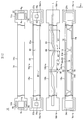
- FIG. 1 is an external perspective view of a high-frequency signal transmission line according to an embodiment of the present invention.
- FIG. 2 is an exploded view of the high-frequency signal transmission line in FIG. 1.
- FIG. 2 is a perspective view of a signal line and an auxiliary ground conductor of the high-frequency signal transmission line in FIG. 1.
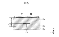
- FIG. 4 is a cross-sectional structure diagram along AA in FIG. 3.
- FIG. 4 is a cross-sectional structure diagram along BB in FIG. 3.
- FIG. 6A is an external perspective view of the connector of the high-frequency signal transmission line.
- FIG. 6B is a cross-sectional structure diagram of the connector of the high-frequency signal transmission line.
- FIG. 7A is a plan view of an electronic device using a high-frequency signal transmission line as viewed from the y-axis direction.
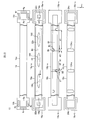
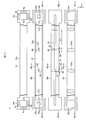
- FIG. 7B is a plan view of an electronic device using the high-frequency signal transmission line as viewed from the z-axis direction. It is an exploded view of the high frequency signal transmission track concerning the 1st modification. It is an exploded view of the high frequency signal transmission track concerning the 2nd modification. It is an exploded view of the high frequency signal transmission track concerning the 3rd modification. It is an exploded view of the high frequency signal transmission track concerning the 4th modification. It is an exploded view of the high frequency signal transmission track concerning the 5th modification. It is an exploded view of the high frequency signal transmission track concerning the 6th modification.
- FIG. 15 is a cross-sectional structure diagram along AA in FIG. 14.
- FIG. 15 is a sectional view taken along line BB in FIG. It is an exploded view of the high frequency signal transmission track concerning the 7th modification. It is an exploded view of the high frequency signal transmission track concerning the 8th modification. It is an exploded view of the high frequency signal transmission track concerning the 9th modification.
- FIG. 1 is an external perspective view of a high-frequency signal transmission line 10 according to an embodiment of the present invention.
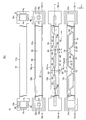
- FIG. 2 is an exploded view of the high-frequency signal transmission line 10 of FIG.
- FIG. 3 is a perspective view of the signal line 20 and the auxiliary ground conductor 24 of the high-frequency signal transmission line 10 of FIG.
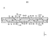
- FIG. 4 is a sectional structural view taken along line AA in FIG.
- FIG. 5 is a cross-sectional structural view taken along line BB in FIG.
- the stacking direction of the high-frequency signal transmission line 10 is defined as the z-axis direction.
- the longitudinal direction of the high-frequency signal transmission line 10 is defined as the x-axis direction, and the direction orthogonal to the x-axis direction and the z-axis direction is defined as the y-axis direction.
- the high-frequency signal transmission line 10 is used for connecting two high-frequency circuits in an electronic device such as a mobile phone. 1 and 2, the high-frequency signal transmission line 10 includes a dielectric body 12, external terminals 16a and 16b, a signal line 20, a reference ground conductor (first ground conductor) 22, and an auxiliary ground conductor (first ground conductor). 2 ground conductors) 24, via-hole conductors (interlayer connection portions) b1, b2, B1 to B4 and connectors 100a and 100b.
- the dielectric body 12 is a flexible plate-like member that extends in the x-axis direction when viewed in plan from the z-axis direction, and includes a line portion 12 a, a connection portion 12 b, 12c is included.
- the dielectric body 12 is a laminated body in which a protective layer 14 and dielectric sheets 18a to 18c are laminated in this order from the positive side in the z-axis direction to the negative side. is there.
- the main surface on the positive side in the z-axis direction of the dielectric body 12 is referred to as the front surface
- the main surface on the negative direction side in the z-axis direction of the dielectric body 12 is referred to as the back surface.
- the line portion 12a extends in the x-axis direction.
- the connecting portions 12b and 12c are respectively connected to the negative end portion in the x-axis direction and the positive end portion in the x-axis direction of the line portion 12a, and have a rectangular shape.
- the width in the y-axis direction of the connection parts 12b and 12c is larger than the width in the y-axis direction of the line part 12a.
- the dielectric sheets 18a to 18c extend in the x-axis direction when viewed in plan from the z-axis direction, and have the same shape as the dielectric body 12.
- the dielectric sheets 18a to 18c are made of flexible thermoplastic resin such as polyimide or liquid crystal polymer.
- the front surface the main surface on the positive side in the z-axis direction of the dielectric sheets 18a to 18c
- the main surface on the negative direction side in the z-axis direction of the dielectric sheets 18a to 18c is referred to as the back surface.
- the thickness T1 of the dielectric sheet 18a is larger than the thickness T2 of the dielectric sheet 18b as shown in FIGS.
- the thickness T1 is, for example, 50 to 300 ⁇ m.
- the thickness T1 is 100 ⁇ m.
- the thickness T2 is, for example, 10 to 100 ⁇ m. In the present embodiment, the thickness T2 is 50 ⁇ m.
- the dielectric sheet 18a includes a line portion 18a-a and connecting portions 18a-b and 18a-c.
- the dielectric sheet 18b includes a line portion 18b-a and connection portions 18b-b and 18b-c.
- the dielectric sheet 18c includes a line portion 18c-a and connection portions 18c-b and 18c-c.
- the line portions 18a-a, 18b-a, and 18c-a constitute the line portion 12a.
- the connecting portions 18a-b, 18b-b, and 18c-b constitute a connecting portion 12b.
- the connecting portions 18a-c, 18b-c, and 18c-c constitute a connecting portion 12c.
- the signal line 20 is a linear conductor that transmits a high-frequency signal and is provided in the dielectric element body 12.
- the signal line 20 is formed on the surface of the dielectric sheet 18b.
- the signal line 20 extends along the x-axis direction in the line portion 18b-a.
- the end of the signal line 20 on the negative direction side in the x-axis direction is located at the center of the connecting portion 18b-b as shown in FIG.
- the end of the signal line 20 on the positive side in the x-axis direction is located at the center of the connecting portion 18b-c.
- the signal line 20 is made of a metal material having a small specific resistance mainly composed of silver or copper.
- the signal line 20 is formed on the surface of the dielectric sheet 18b means that the signal line 20 is formed by patterning a metal foil formed by plating on the surface of the dielectric sheet 18b, It means that the signal line 20 is formed by patterning the metal foil attached to the surface of the dielectric sheet 18b. Further, since the surface of the signal line 20 is smoothed, the surface roughness of the surface where the signal line 20 is in contact with the dielectric sheet 18b is the surface roughness of the surface where the signal line 20 is not in contact with the dielectric sheet 18b. It becomes larger than the roughness.
- the reference ground conductor 22 is a solid conductor layer provided on the positive side in the z-axis direction from the signal line 20. More specifically, the reference ground conductor 22 is formed on the surface of the dielectric sheet 18a and faces the signal line 20 through the dielectric sheet 18a. The reference ground conductor 22 is not provided with an opening at a position overlapping the signal line 20.
- the reference ground conductor 22 is made of a metal material having a small specific resistance mainly composed of silver or copper.
- the reference ground conductor 22 is formed on the surface of the dielectric sheet 18a. That is, the reference ground conductor 22 is formed by patterning a metal foil formed by plating on the surface of the dielectric sheet 18a.
- the reference ground conductor 22 is formed by patterning the metal foil attached to the surface of the dielectric sheet 18a. Further, since the surface of the reference ground conductor 22 is smoothed, the surface roughness of the surface where the reference ground conductor 22 is in contact with the dielectric sheet 18a is not in contact with the dielectric sheet 18a. It becomes larger than the surface roughness of the surface.
- the reference ground conductor 22 includes a line portion 22a and terminal portions 22b and 22c.
- the line portion 22a is provided on the surface of the line portion 18a-a and extends along the x-axis direction.
- the terminal portion 22b is provided on the surface of the line portion 18a-b and forms a rectangular ring.
- the terminal portion 22b is connected to the end portion on the negative direction side in the x-axis direction of the line portion 22a.
- the terminal portion 22c is provided on the surface of the line portion 18a-c and forms a rectangular ring.
- the terminal portion 22c is connected to the end portion on the positive direction side in the x-axis direction of the line portion 22a.
- the auxiliary ground conductor 24 is provided on the negative side in the z-axis direction from the signal line 20.
- the auxiliary ground conductor 24 is provided with a plurality of openings 30 and 32 arranged along the signal line 20. More specifically, the auxiliary ground conductor 24 is formed on the surface of the dielectric sheet 18c and faces the signal line 20 through the dielectric sheet 18b.
- the auxiliary ground conductor 24 is made of a metal material having a small specific resistance mainly composed of silver or copper.
- the auxiliary ground conductor 24 is formed on the surface of the dielectric sheet 18c means that the auxiliary ground conductor 24 is formed by patterning a metal foil formed by plating on the surface of the dielectric sheet 18c.
- the auxiliary ground conductor 24 is formed by patterning a metal foil attached to the surface of the dielectric sheet 18c. Further, since the surface of the auxiliary ground conductor 24 is smoothed, the surface roughness of the surface where the auxiliary ground conductor 24 is in contact with the dielectric sheet 18c is not in contact with the dielectric sheet 18c. It becomes larger than the surface roughness of the surface.
- the auxiliary ground conductor 24 includes a line portion 24a and terminal portions 24b and 24c.
- the line portion 24a is provided on the surface of the line portion 18c-a, and extends along the x-axis direction.
- the terminal portion 24b is provided on the surface of the line portion 18c-b and forms a rectangular ring.
- the terminal portion 24b is connected to the end portion on the negative direction side in the x-axis direction of the line portion 24a.
- the terminal portion 24c is provided on the surface of the line portion 18c-c and forms a rectangular ring.
- the terminal portion 24c is connected to the end portion on the positive direction side in the x-axis direction of the line portion 24a.
- the line portion 24a is provided with a plurality of openings 30, 32 having a parallelogram shape extending in the x-axis direction. More specifically, the line portion 24a includes a plurality of connection portions 70 and 72, sides 74 and 76, and a plurality of bridge portions 78, 80, 86, and 88.
- the side 74 is a linear conductor that forms a side on the negative direction side in the y-axis direction of the line portion 24a, and extends in the x-axis direction.
- the side 76 is a linear conductor that forms a side on the positive direction side in the y-axis direction of the line portion 24a, and extends in the x-axis direction.
- the plurality of connecting portions 70 protrude from the side 74 to the positive direction side in the y-axis direction and have a semicircular shape.
- the plurality of connection portions 70 are arranged in a line at equal intervals in the x-axis direction.
- the plurality of connecting portions 72 protrude from the side 76 to the negative direction side in the y-axis direction and have a semicircular shape.
- the plurality of connection portions 72 are arranged in a line at equal intervals in the x-axis direction.
- the connection part 70 and the connection part 72 are provided at different positions in the x-axis direction. In the present embodiment, the connection portions 70 and the connection portions 72 are alternately arranged in the x-axis direction.
- connection part 72 is located in the middle of the two connection parts 70 adjacent in the x-axis direction in the x-axis direction.
- connection part 70 is located in the middle of two connection parts 72 adjacent in the x-axis direction in the x-axis direction.
- the bridge portion 78 is a linear conductor that is inclined so as to advance from the connection portion 70 to the positive direction side in the y-axis direction and to the positive direction side in the x-axis direction, and is connected to the side 76.
- the bridge portion 80 is a linear conductor that is inclined so as to advance from the connection portion 72 to the negative direction side in the y-axis direction and to the negative direction side in the x-axis direction, and is connected to the side 74.
- the bridge part 78 and the bridge part 80 are parallel. Thereby, an opening 30 is formed in a region surrounded by the sides 74 and 76 and the bridge portions 78 and 80.
- the bridge portion 86 is a linear conductor that is inclined so as to advance from the connection portion 72 in the negative direction side in the y-axis direction to the positive direction side in the x-axis direction, and is connected to the side 74.
- the bridge portion 88 is a linear conductor that is inclined so as to advance from the connection portion 70 toward the positive direction side in the y-axis direction while traveling toward the negative direction side in the x-axis direction, and is connected to the side 76.
- the bridge part 86 and the bridge part 88 are parallel. Thereby, the opening 32 is formed in a region surrounded by the sides 74 and 76 and the bridge portions 86 and 88.
- a notch C1 is provided in the side 74 of the line portion 24a.
- the notch C1 is provided on the negative direction side in the y-axis direction with respect to the connection portion 72 in the line portion 24a. As a result, the side 74 is separated at the notch C1.
- a notch C2 is provided in the side 76 of the line portion 24a.
- the notch C2 is provided on the positive side in the y-axis direction with respect to the connection portion 70 in the line portion 24a. As a result, the side 76 is separated at the notch C2.
- the external terminal 16a is a rectangular conductor formed substantially at the center on the surface of the connecting portion 18a-b. Therefore, the external terminal 16a overlaps the end of the signal line 20 on the negative direction side in the x-axis direction when viewed in plan from the z-axis direction.
- the external terminal 16b is a rectangular conductor formed substantially at the center on the surface of the connecting portion 18a-c. Therefore, the external terminal 16b overlaps the end of the signal line 20 on the positive direction side in the x-axis direction when viewed in plan from the z-axis direction.
- the external terminals 16a and 16b are made of a metal material having a small specific resistance mainly composed of silver or copper.
- Ni / Au plating is applied to the surfaces of the external terminals 16a and 16b.
- the external terminals 16a and 16b are formed on the surface of the dielectric sheet 18a.
- the metal foil formed by plating on the surface of the dielectric sheet 18a is patterned to form the external terminals 16a and 16b. It indicates that the external terminals 16a and 16b are formed by patterning the metal foil attached to the surface of the dielectric sheet 18a. Since the surfaces of the external terminals 16a and 16b are smoothed, the surface roughness of the surface where the external terminals 16a and 16b are in contact with the dielectric sheet 18a is the same as that of the external terminals 16a and 16b. It becomes larger than the surface roughness of the non-contact surface.
- the signal line 20 is sandwiched between the reference ground conductor 22 and the auxiliary ground conductor 24 from the z-axis direction. That is, the signal line 20, the reference ground conductor 22, and the auxiliary ground conductor 24 have a triplate type stripline structure. Further, the distance (distance in the z-axis direction) between the signal line 20 and the reference ground conductor 22 is substantially equal to the thickness T1 of the dielectric sheet 18a as shown in FIG. 4, and is, for example, 50 ⁇ m to 300 ⁇ m. In the present embodiment, the distance between the signal line 20 and the reference ground conductor 22 is 100 ⁇ m.
- the distance (distance in the z-axis direction) between the signal line 20 and the auxiliary ground conductor 24 is substantially equal to the thickness T2 of the dielectric sheet 18b as shown in FIG. 4, for example, 10 ⁇ m to 100 ⁇ m.
- the distance between the signal line 20 and the auxiliary ground conductor 24 is 50 ⁇ m. That is, the distance between the auxiliary ground conductor 24 and the signal line 20 in the z-axis direction is designed to be smaller than the distance between the reference ground conductor 22 and the signal line 20 in the z-axis direction.
- the via-hole conductor b1 passes through the connecting portion 18a-b of the dielectric sheet 18a in the z-axis direction, and the end of the external terminal 16a and the signal line 20 on the negative direction side in the x-axis direction. And connected.
- the via-hole conductor b2 passes through the connecting portion 18a-c of the dielectric sheet 18a in the z-axis direction, and is the end of the external terminal 16b and the signal line 20 on the positive direction side in the x-axis direction. And connected. Thereby, the signal line 20 is connected between the external terminals 16a and 16b.
- the via-hole conductors b1 and b2 are formed by filling a metal material in a through hole formed in the dielectric sheet 18a.
- the plurality of via-hole conductors B1 penetrate the line portion 18a-a in the z-axis direction on the negative direction side in the y-axis direction from the signal line 20, and are aligned in the x-axis direction. Are lined up. As shown in FIGS. 2 and 3, the plurality of via-hole conductors B2 pass through the line portion 18b-a in the z-axis direction on the negative direction side in the y-axis direction from the signal line 20, and are aligned in the x-axis direction. Are lined up.
- the via-hole conductors B1 and B2 are provided on the negative direction side in the y-axis direction from the center line L in the y-axis direction (width direction) of the high-frequency signal transmission line 10.
- the via hole conductor B1 and the via hole conductor B2 constitute a single via hole conductor by being connected to each other.
- the end portion on the positive direction side in the z-axis direction of the via-hole conductor B1 is connected to the reference ground conductor 22, and the end portion on the negative direction side in the z-axis direction of the via-hole conductor B2 is connected to the connection portion 70. .
- the via-hole conductors B ⁇ b> 1 and B ⁇ b> 2 connect the reference ground conductor 22 and the auxiliary ground conductor 24.
- the via-hole conductors B1 and B2 are formed by filling a metal material in through holes formed in the dielectric sheets 18a and 18b.
- a section in which the via-hole conductors B1 and B2 are provided is referred to as a section A2.
- the section A2 means a region overlapping with the via-hole conductors B1 and B2 in the y-axis direction.
- the plurality of via-hole conductors B3 penetrate the line portion 18a-a in the z-axis direction on the positive side in the y-axis direction from the signal line 20, and are aligned in the x-axis direction. Are lined up. As shown in FIGS. 2 and 3, the plurality of via-hole conductors B4 pass through the line portion 18b-a in the z-axis direction on the positive side in the y-axis direction from the signal line 20, and are aligned in the x-axis direction. Are lined up.
- the via-hole conductors B3 and B4 are provided on the positive direction side in the y-axis direction from the center line L in the y-axis direction (width direction) of the high-frequency signal transmission line 10.
- the via-hole conductor B3 and the via-hole conductor B4 constitute one via-hole conductor by being connected to each other.
- the end portion on the positive direction side in the z-axis direction of the via-hole conductor B3 is connected to the reference ground conductor 22, and the end portion on the negative direction side in the z-axis direction of the via-hole conductor B4 is connected to the connection portion 72.
- the via-hole conductors B3 and B4 connect the reference ground conductor 22 and the auxiliary ground conductor 24.
- the via-hole conductors B3 and B4 are formed by filling a metal material in through holes formed in the dielectric sheets 18a and 18b.
- a section where the via-hole conductors B3 and B4 are provided is referred to as a section A3.
- the section A3 means a region overlapping with the via-hole conductors B3 and B4 in the y-axis direction.
- the via-hole conductors B1 and B2 and the via-hole conductors B3 and B4 are provided at different positions in the x-axis direction.
- the via hole conductors B1 and B2 and the via hole conductors B3 and B4 are alternately arranged in the x-axis direction.
- the via-hole conductors B1 and B2 are located in the middle of two via-hole conductors B3 and B4 adjacent in the x-axis direction in the x-axis direction.
- the via-hole conductors B3 and B4 are located in the middle of two via-hole conductors B1 and B2 adjacent in the x-axis direction in the x-axis direction.
- a section sandwiched between the section A2 and the section A3 is referred to as a section A1.
- the section A1 is a section where the via-hole conductors B1 to B4 are not provided.
- the signal line 20 meanders as shown in FIG. More specifically, the signal line 20 in the section A1 is located closer to the negative direction side in the y-axis direction than the signal line 20 in the section A2. Further, the signal line 20 in the section A1 is located on the positive side in the y-axis direction than the signal line 20 in the section A3. As a result, the signal line 20 bypasses the via-hole conductors B1 and B2 and the via-hole conductors B3 and B4.
- the signal line 20 has thick line portions 50, 52, 54 and thin line portions 56, 58, 60, 62.
- the line width of the thick line portions 50, 52, 54 is the line width W1.
- the line width of the thin line portions 56, 58, 60, 62 is the line width W2.
- the line width W1 is larger than the line width W2.
- the thick line portion 50 extends in the x-axis direction on the center line L in the y-axis direction of the line portion 18b-a in the section A1.
- the thick line portion 50 overlaps the openings 30 and 32 when viewed in plan from the z-axis direction. Therefore, the thick line portion 50 does not overlap the auxiliary ground conductor 24 when viewed in plan from the z-axis direction.
- the thick line portion 52 extends in the x-axis direction in the positive direction side in the y-axis direction from the center line L in the y-axis direction of the line portion 18b-a in the section A2. However, both ends in the x-axis direction of the thick line portion 52 protrude into the section A1.
- the thick line portion 52 overlaps the notch C2 when viewed in plan from the z-axis direction. Therefore, the thick line portion 52 does not overlap the auxiliary ground conductor 24 when viewed in plan from the z-axis direction.
- the thick line portion 54 extends in the x-axis direction on the negative direction side in the y-axis direction from the center line L in the y-axis direction of the line portion 18b-a. However, both ends in the x-axis direction of the thick line portion 52 protrude into the section A1.
- the thick line portion 54 overlaps the notch C1 when viewed in plan from the z-axis direction. Therefore, the thick line portion 54 does not overlap the auxiliary ground conductor 24 when viewed in plan from the z-axis direction. Both ends of the thick line portions 50, 52, 54 as described above are tapered.
- the thin line portion 56 connects the end portion on the positive direction side in the x-axis direction of the thick line portion 52 and the end portion on the negative direction side in the x-axis direction of the thick line portion 50 in the section A1.
- the thin line portion 56 is inclined so as to advance toward the positive direction side in the x-axis direction while proceeding toward the negative direction side in the y-axis direction. Further, as shown in FIG. 3, the thin line portion 56 overlaps the bridge portion 78 when viewed in plan from the y-axis direction.
- the thin line portion 58 connects the end portion on the positive side in the x-axis direction of the thick line portion 50 and the end portion on the negative direction side in the x-axis direction of the thick line portion 54 in the section A1.
- the thin wire portion 58 is inclined so as to advance toward the positive direction side in the x-axis direction while proceeding toward the negative direction side in the y-axis direction. Further, as shown in FIG. 3, the thin line portion 58 overlaps the bridge portion 80 when viewed in plan from the y-axis direction.
- the fine line portion 60 connects the end portion on the positive direction side in the x-axis direction of the thick line portion 50 and the end portion on the negative direction side in the x-axis direction of the thick line portion 52 in the section A1.
- the thin line portion 60 is inclined so as to advance toward the positive direction side in the x-axis direction while traveling toward the positive direction side in the y-axis direction. Further, as shown in FIG. 3, the thin line portion 60 overlaps the bridge portion 88 when viewed in plan from the y-axis direction.
- the thin line portion 62 connects the end portion on the positive direction side in the x-axis direction of the thick line portion 54 and the end portion on the negative direction side in the x-axis direction of the thick line portion 50 in the section A1.
- the thin wire portion 62 is inclined so as to advance toward the positive direction side in the x-axis direction while traveling toward the positive direction side in the y-axis direction. Further, as shown in FIG. 3, the thin line portion 62 overlaps the bridge portion 86 when viewed in plan from the y-axis direction.
- the protective layer 14 is an insulating film that covers substantially the entire surface of the dielectric sheet 18a. Thereby, the protective layer 14 covers the reference ground conductor 22.
- the protective layer 14 is made of a flexible resin such as a resist material, for example.
- the protective layer 14 includes a line portion 14a and connecting portions 14b and 14c.
- the line portion 14a covers the line portion 22a by covering the entire surface of the line portion 18a-a.
- the connecting portion 14b is connected to the end portion on the negative side in the x-axis direction of the line portion 14a and covers the surface of the connecting portion 18a-b.
- openings Ha to Hd are provided in the connection portion 14b.
- the opening Ha is a rectangular opening provided in the center of the connection portion 14b.
- the external terminal 16a is exposed to the outside through the opening Ha.
- the opening Hb is a rectangular opening provided on the positive side in the y-axis direction with respect to the opening Ha.
- the opening Hc is a rectangular opening provided on the negative direction side in the x-axis direction from the opening Ha.
- the opening Hd is a rectangular opening provided on the negative side in the y-axis direction with respect to the opening Ha.
- the terminal portion 22b functions as an external terminal by being exposed to the outside through the openings Hb to Hd.
- the connecting portion 14c is connected to the end portion on the positive side in the x-axis direction of the line portion 14a and covers the surface of the connecting portion 18a-c.
- openings He to Hh are provided in the connection portion 14c.
- the opening He is a rectangular opening provided in the center of the connection portion 14c.
- the external terminal 16b is exposed to the outside through the opening He.
- the opening Hf is a rectangular opening provided on the positive direction side in the y-axis direction with respect to the opening He.
- the opening Hg is a rectangular opening provided closer to the positive direction side in the x-axis direction than the opening He.
- the opening Hh is a rectangular opening provided on the negative side in the y-axis direction with respect to the opening He.
- the terminal portion 22c functions as an external terminal by being exposed to the outside through the openings Hf to Hh.
- the characteristic impedance of the signal line 20 periodically varies between the impedance Z1 and the impedance Z2. More specifically, a relatively small capacitance is formed between the signal line 20 and the auxiliary ground conductor 24 at a portion of the signal line 20 that overlaps the openings 30 and 32 and the cutouts C1 and C2. Therefore, the characteristic impedance of the portion of the signal line 20 that overlaps the openings 30 and 32 and the notches C1 and C2 is a relatively high impedance Z1.
- the characteristic impedance of the portion of the signal line 20 that overlaps the bridge portions 78, 80, 86, and 88 is a relatively low impedance Z2.
- the bridge portion 78, the opening 30, the bridge portion 80, the notch C1, the bridge portion 86, the opening 32, the bridge portion 88, and the notch C2 are arranged in the x-axis direction in this order. Therefore, the characteristic impedance of the signal line 20 periodically varies between the impedance Z1 and the impedance Z2.
- the impedance Z1 is, for example, 55 ⁇
- the impedance Z2 is, for example, 45 ⁇ .
- the average characteristic impedance of the entire signal line 20 is, for example, 50 ⁇ .
- FIG. 6A is an external perspective view of the connector 100 b of the high-frequency signal transmission line 10.
- FIG. 6B is a cross-sectional structure diagram of the connector 100 b of the high-frequency signal transmission line 10.
- the connector 100b includes a connector body 102, external terminals 104 and 106, a central conductor 108, and an external conductor 110, as shown in FIGS. 1, 6A, and 6B.
- the connector main body 102 has a shape in which a cylindrical member is connected to a rectangular plate member, and is made of an insulating material such as a resin.
- the external terminal 104 is provided at a position facing the external terminal 16b on the negative side surface in the z-axis direction of the plate member of the connector main body 102.
- the external terminal 106 is provided at a position corresponding to the terminal portion 22c exposed through the openings Hf to Hh on the negative surface side in the z-axis direction of the plate member of the connector main body 102.
- the center conductor 108 is provided at the center of the cylindrical member of the connector main body 102 and is connected to the external terminal 104.
- the center conductor 108 is a signal terminal for inputting or outputting a high frequency signal.
- the external conductor 110 is provided on the inner peripheral surface of the cylindrical member of the connector main body 102 and is connected to the external terminal 106.
- the outer conductor 110 is a ground terminal that is maintained at a ground potential.
- the external terminal 104 is connected to the external terminal 16b, and the external terminal 106 is connected to the terminal portion 22c. And mounted on the surface of the connecting portion 12c. Thereby, the signal line 20 is electrically connected to the central conductor 108. Further, the reference ground conductor 22 and the auxiliary ground conductor 24 are electrically connected to the external conductor 110.
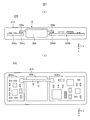
- FIG. 7A is a plan view of the electronic device 200 using the high-frequency signal transmission line 10 from the y-axis direction.
- FIG. 7B is a plan view of the electronic device 200 in which the high-frequency signal transmission line 10 is used from the z-axis direction.
- the electronic device 200 includes the high-frequency signal transmission line 10, circuit boards 202 a and 202 b, receptacles 204 a and 204 b, a battery pack (metal body) 206, and a casing 210.
- the housing 210 houses the high-frequency signal transmission line 10, the circuit boards 202a and 202b, the receptacles 204a and 204b, and the battery pack 206.
- the circuit board 202a is provided with, for example, a transmission circuit or a reception circuit including an antenna.
- a power supply circuit is provided on the circuit board 202b.
- the battery pack 206 is a lithium ion secondary battery, for example, and has a structure in which the surface is covered with a metal cover.
- the circuit board 202a, the battery pack 206, and the circuit board 202b are arranged in this order from the negative direction side to the positive direction side in the x-axis direction.
- the receptacles 204a and 204b are provided on the main surfaces of the circuit boards 202a and 202b on the negative side in the z-axis direction, respectively.
- Connectors 100a and 100b are connected to receptacles 204a and 204b, respectively.
- a high frequency signal having a frequency of, for example, 2 GHz transmitted between the circuit boards 202a and 202b is applied to the central conductor 108 of the connectors 100a and 100b via the receptacles 204a and 204b.
- the external conductor 110 of the connectors 100a and 100b is kept at the ground potential via the circuit boards 202a and 202b and the receptacles 204a and 204b.
- the high frequency signal transmission line 10 connects between the circuit boards 202a and 202b.
- the surface of the dielectric body 12 (more precisely, the protective layer 14) is in contact with the battery pack 206.
- the dielectric body 12 and the battery pack 206 are fixed with an adhesive or the like.
- the surface of the dielectric body 12 is a main surface located on the reference ground conductor 22 side with respect to the signal line 20. Therefore, the solid reference ground conductor 22 is located between the signal line 20 and the battery pack 206.
- dielectric sheets 18a to 18c made of a thermoplastic resin having a copper foil (metal film) formed on the entire surface are prepared. Specifically, copper foil is attached to the surfaces of the dielectric sheets 18a to 18c. Further, the surface of the copper foil of the dielectric sheets 18a to 18c is smoothed by applying, for example, zinc plating for rust prevention.
- the dielectric sheets 18a to 18c are liquid crystal polymers. The thickness of the copper foil is 10 ⁇ m to 20 ⁇ m.
- the external terminals 16a and 16b and the reference ground conductor 22 shown in FIG. 2 are formed on the surface of the dielectric sheet 18a.
- a resist having the same shape as the external terminals 16a and 16b and the reference ground conductor 22 shown in FIG. 2 is printed on the copper foil on the surface of the dielectric sheet 18a.
- the copper foil of the part which is not covered with the resist is removed by performing an etching process with respect to copper foil. Thereafter, a resist solution is sprayed to remove the resist.
- the external terminals 16a and 16b and the reference ground conductor 22 as shown in FIG. 2 are formed on the surface of the dielectric sheet 18a by a photolithography process.
- the signal line 20 shown in FIG. 2 is formed on the surface of the dielectric sheet 18b. Further, the auxiliary ground conductor 24 shown in FIG. 2 is formed on the surface of the dielectric sheet 18c. In addition, since the formation process of the signal line 20 and the auxiliary ground conductor 24 is the same as the formation process of the external terminals 16a and 16b and the reference ground conductor 22, the description thereof is omitted.
- a through hole is formed by irradiating a laser beam to a position where the via hole conductors b1, b2, B1 to B4 of the dielectric sheets 18a and 18b are formed. Then, the through hole is filled with a conductive paste to form via-hole conductors b1, b2, B1 to B4.
- the dielectric sheets 18a to 18c are stacked in this order from the positive direction side in the z-axis direction to the negative direction side to form the dielectric element body 12. Then, the dielectric sheets 18a to 18c are integrated by applying heat and pressure to the dielectric sheets 18a to 18c from the positive and negative directions in the z-axis direction.
- a protective layer 14 covering the reference ground conductor 22 is formed on the surface of the dielectric sheet 18a by applying a resin (resist) paste by screen printing.
- the connectors 100a and 100b are mounted on the external terminals 16a and 16b on the connection parts 12b and 12c and the terminal parts 22b and 22c by using solder. Thereby, the high frequency signal transmission line 10 shown in FIG. 1 is obtained.
- the width of the dielectric element body 12 in the y-axis direction can be reduced. More specifically, in the high-frequency signal transmission line 10, the via-hole conductors B ⁇ b> 1 and B ⁇ b> 2 are provided in the dielectric element body 12 on the negative direction side in the y-axis direction with respect to the center line L in the y-axis direction. Furthermore, the signal line 20 in the section A2 where the via-hole conductors B1 and B2 are provided is located on the positive side in the y-axis direction than the signal line 20 in the section A1 where the via-hole conductors B1 and B2 are not provided. Yes. That is, the signal line 20 bypasses the via-hole conductors B1 and B2 when viewed in plan from the z-axis direction. Thereby, the via-hole conductors B1 and B2 can be brought close to the center line L.
- the via-hole conductors B3 and B4 are provided in the dielectric element body 12 on the positive direction side in the y-axis direction with respect to the center line L in the y-axis direction. Further, the signal line 20 in the section A3 where the via-hole conductors B3 and B4 are provided is located on the negative side in the y-axis direction than the signal line 20 in the section A1 where the via-hole conductors B3 and B4 are not provided. Yes. Thus, the signal line 20 bypasses the via-hole conductors B3 and B4 when viewed in plan from the z-axis direction. As a result, the via-hole conductors B3 and B4 can be brought closer to the center line L.
- the via-hole conductors B1 and B2 and the via-hole conductors B3 and B4 are provided at different positions in the x-axis direction.
- the via-hole conductors B1 and B2, the signal line 20, and the via-hole conductors B3 and B4 are not arranged in a line in the y-axis direction. Therefore, the side on the positive direction side in the y-axis direction of the line portion 12a can be brought closer to the center line L, and the side on the negative direction side in the y-axis direction of the line portion 12a can be brought closer to the center line L. As a result, the width of the dielectric body 12 in the y-axis direction can be reduced.
- the auxiliary ground conductor 24 is provided with openings 30, 32 and notches C1, C2. This makes it difficult for a capacitance to be formed between the signal line 20 and the auxiliary ground conductor 24. Therefore, even if the distance between the signal line 20 and the auxiliary ground conductor 24 in the z-axis direction is reduced, the capacitance formed between the signal line 20 and the auxiliary ground conductor 24 does not become too large. Therefore, the characteristic impedance of the signal line 20 is unlikely to deviate from a predetermined characteristic impedance (for example, 50 ⁇ ). As a result, according to the high-frequency signal transmission line 10, it is possible to reduce the thickness while maintaining the characteristic impedance of the signal line 20 at a predetermined characteristic impedance.
- a predetermined characteristic impedance for example, 50 ⁇
- the insertion loss can be reduced.
- the auxiliary ground conductor 24 is provided with openings 30 and 32 and notches C1 and C2. Therefore, in the signal line 20, it is difficult to form a capacitance between the portion overlapping the openings 30 and 32 and the notches C ⁇ b> 1 and C ⁇ b> 2 and the auxiliary ground conductor 24. Therefore, the thick line portions 50 and 52 of the signal line 20 are arranged so as to overlap the openings 30 and 32 and the cutouts C1 and C2. Thereby, the resistance value of the signal line 20 is reduced, and the insertion loss of the high-frequency signal transmission line 10 is reduced.
- the high-frequency signal transmission line 10 when the high-frequency signal transmission line 10 is attached to a metal body such as the battery pack 206, the characteristic impedance of the signal line 20 is suppressed from fluctuating. More specifically, the high-frequency signal transmission line 10 is attached to the battery pack 206 so that the solid reference ground conductor 22 is located between the signal line 20 and the battery pack 206. As a result, the signal line 20 and the battery pack 206 do not face each other through the opening, and the formation of a capacitance between the signal line 20 and the battery pack 206 is suppressed. As a result, the high-frequency signal transmission line 10 is affixed to the battery pack 206, thereby suppressing the characteristic impedance of the signal line 20 from being lowered.
- the via-hole conductors B ⁇ b> 1 and B ⁇ b> 2 are provided on the negative direction side in the y-axis direction with respect to the signal line 20.
- the via-hole conductors B3 and B4 are provided on the positive side in the y-axis direction with respect to the signal line 20.
- unnecessary radiation is suppressed from being emitted to both sides of the signal line 20 in the y-axis direction.
- the via-hole conductor B1 is interposed between the signal line 20 and the battery pack 206.
- B2 or via-hole conductors B3, B4 are present. As a result, it is difficult to form a capacity between the signal line 20 and the battery pack 206, and fluctuations in the characteristic impedance of the signal line 20 are suppressed.
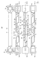
- FIG. 8 is an exploded view of the high-frequency signal transmission line 10a according to the first modification.
- FIG. 1 is used for an external perspective view of the high-frequency signal transmission line 10a.
- the high-frequency signal transmission line 10 a is different from the high-frequency signal transmission line 10 in that the reference ground conductor 22 has the same structure as the auxiliary ground conductor 24. More specifically, as shown in FIG. 8, the line portion 22a of the reference ground conductor 22 is provided with a plurality of openings 130 and 132 having a parallelogram shape extending in the x-axis direction. The openings 130 and 132 are arranged along the signal line 20.
- the line portion 22a has a plurality of connection portions 170, 172, sides 174, 176, and a plurality of bridge portions 178, 180, 186, 188.
- the side 174 is a linear conductor constituting the side on the negative direction side in the y-axis direction of the line portion 22a, and extends in the x-axis direction.
- the side 176 is a linear conductor constituting the side on the positive direction side in the y-axis direction of the line portion 22a and extends in the x-axis direction.
- the plurality of connecting portions 170 protrude from the side 174 to the positive direction side in the y-axis direction and have a semicircular shape.
- the plurality of connecting portions 170 are arranged in a line at equal intervals in the x-axis direction.
- the plurality of connecting portions 172 protrude from the side 176 to the negative direction side in the y-axis direction and have a semicircular shape.
- the plurality of connecting portions 172 are arranged in a line at equal intervals in the x-axis direction.
- the connecting portion 170 and the connecting portion 172 are provided at different positions in the x-axis direction.
- the connection portions 170 and the connection portions 172 are alternately arranged in the x-axis direction.
- the connection part 172 is located in the middle of the two connection parts 170 adjacent to the x-axis direction in the x-axis direction.
- the connection part 170 is located in the middle of two connection parts 172 adjacent in the x-axis direction in the x-axis direction.
- the bridge portion 178 is a linear conductor that is inclined so as to advance from the connecting portion 170 to the positive direction side in the y-axis direction and to the positive direction side in the x-axis direction, and is connected to the side 176.
- the bridge portion 180 is a linear conductor that is inclined from the connecting portion 172 so as to travel toward the negative direction side in the x-axis direction while traveling toward the negative direction side in the y-axis direction, and is connected to the side 176.
- the bridge part 178 and the bridge part 180 are parallel. As a result, an opening 130 is formed in a region surrounded by the sides 174 and 176 and the bridge portions 178 and 180. The opening 130 overlaps with the opening 30 when viewed in plan from the z-axis direction.
- the bridge portion 186 is a linear conductor that is inclined so as to advance from the connection portion 172 to the negative direction side in the y-axis direction and to the positive direction side in the x-axis direction, and is connected to the side 174.
- the bridge portion 188 is a linear conductor that is inclined so as to travel from the connection portion 170 to the positive side in the y-axis direction and to the negative direction side in the x-axis direction, and is connected to the side 176.
- the bridge portion 186 and the bridge portion 188 are parallel. Thereby, an opening 132 is formed in a region surrounded by the sides 174 and 176 and the bridge portions 186 and 188. The opening 132 overlaps with the opening 32 in a plan view from the z-axis direction.
- a notch C3 is provided in the side 174 of the line portion 22a.
- the notch C3 is provided in the negative direction side in the y-axis direction with respect to the connection portion 172 in the line portion 22a. Thereby, the side 174 is separated at the notch C3.
- a notch C4 is provided in the side 176 of the line portion 22a.
- the notch C4 is provided on the positive side in the y-axis direction with respect to the connection portion 170 in the line portion 22a. As a result, the side 176 is separated at the notch C4.
- the width of the dielectric element body 12 in the y-axis direction can be reduced as in the high-frequency signal transmission line 10.
- the reference ground conductor 22 is also provided with openings 130 and 132 and notches C3 and C4. This makes it difficult to form a capacitor between the signal line 20 and the reference ground conductor 22. Therefore, even if the distance between the signal line 20 and the reference ground conductor 22 in the z-axis direction is reduced, the capacitance formed between the signal line 20 and the reference ground conductor 22 does not become too large. Therefore, the characteristic impedance of the signal line 20 is unlikely to deviate from a predetermined characteristic impedance (for example, 50 ⁇ ). As a result, according to the high-frequency signal transmission line 10, it is possible to reduce the thickness while maintaining the characteristic impedance of the signal line 20 at a predetermined characteristic impedance.
- a predetermined characteristic impedance for example, 50 ⁇
- the insertion loss can be reduced.
- the high-frequency signal transmission line 10 a similarly to the high-frequency signal transmission line 10, fluctuations in the characteristic impedance of the signal line 20 are suppressed.
- FIG. 9 is an exploded view of the high-frequency signal transmission line 10b according to the second modification.
- FIG. 1 is used for an external perspective view of the high-frequency signal transmission line 10b.
- the high-frequency signal transmission line 10 b is different from the high-frequency signal transmission line 10 in the structure of the signal line 20. More specifically, in the high-frequency signal transmission line 10b, the line width of the signal line 20 is uniform.
- the width of the dielectric element body 12 in the y-axis direction can be reduced.
- the thickness can be further reduced.
- the high-frequency signal transmission line 10 b similarly to the high-frequency signal transmission line 10, fluctuations in the characteristic impedance of the signal line 20 are suppressed.
- FIG. 10 is an exploded view of the high-frequency signal transmission line 10c according to the third modification.
- FIG. 1 is used for an external perspective view of the high-frequency signal transmission line 10c.
- the high frequency signal transmission line 10c is different from the high frequency signal transmission line 10a in the size of the openings 130 and 132. More specifically, the size of the opening 130 is smaller than the size of the opening 30.
- the opening 130 has a similar shape to the opening 30 when viewed in plan from the z-axis direction, and is accommodated in the opening 30.
- the size of the opening 132 is smaller than the size of the opening 32.
- the opening 132 has a similar shape to the opening 32 when viewed in plan from the z-axis direction, and is accommodated in the opening 32.
- the width of the dielectric element body 12 in the y-axis direction can be reduced in the same manner as the high-frequency signal transmission line 10a.
- the high-frequency signal transmission line 10c it is possible to further reduce the thickness, similarly to the high-frequency signal transmission line 10a.
- the insertion loss can be reduced also for the following reason.
- a current i 1 flows through the signal line 20
- a feedback current (countercurrent) i 2 flows through the reference ground conductor 22
- a feedback current (countercurrent) i 3 flows through the auxiliary ground conductor 24.
- the outer edge of the opening 30 and the outer edge of the opening 130 do not overlap.
- the outer edge of the opening 32 and the outer edge of the opening 132 do not overlap.
- the position where the feedback current i2 flows is separated from the position where the feedback current i3 flows.
- the coupling between the feedback current i2 and the feedback current i3 can be weakened, and the current i1 can easily flow. Therefore, the insertion loss of the high-frequency signal transmission line 10c can be reduced.
- the characteristic impedance of the signal line 20 is suppressed from fluctuating in the same manner as the high-frequency signal transmission line 10a.
- FIG. 11 is an exploded view of the high-frequency signal transmission line 10d according to the fourth modification.
- FIG. 1 is used for an external perspective view of the high-frequency signal transmission line 10d.
- the high-frequency signal transmission line 10 d is different from the high-frequency signal transmission line 10 in the structure of the auxiliary ground conductor 24 and the structure of the signal line 20. More specifically, notches C1 and C2 are not provided in the auxiliary ground conductor 24 of the high-frequency signal transmission line 10d. That is, the sides 74 and 76 are not cut and are constituted by one linear conductor. Therefore, an opening 150 surrounded by the side 74 and the bridge portions 80 and 86 is formed. An opening 152 surrounded by the side 76 and the bridge portions 78 and 88 is formed.
- the line width of the portion overlapping the openings 150 and 152 is smaller than the line width of the portion overlapping the openings 30 and 32. This is to prevent the signal line 20 and the sides 74 and 76 from overlapping in the sections A2 and A3.
- the width of the dielectric element body 12 in the y-axis direction can be reduced as in the high-frequency signal transmission line 10.
- the thickness can be further reduced.
- the insertion loss can be reduced.
- the high-frequency signal transmission line 10 d similarly to the high-frequency signal transmission line 10, fluctuations in the characteristic impedance of the signal line 20 are suppressed.
- the cutouts C1 and C2 are not provided in the sides 74 and 76, so that unnecessary radiation is suppressed from being emitted from the signal line 20.
- FIG. 12 is an exploded view of the high-frequency signal transmission line 10e according to the fifth modification.
- FIG. 1 is used for an external perspective view of the high-frequency signal transmission line 10e.
- the high-frequency signal transmission line 10e is different from the high-frequency signal transmission line 10d in the structure of the auxiliary ground conductor 24.
- rectangular openings 230 extending in the x-axis direction are provided in the line portion 24 a of the auxiliary ground conductor 24 so as to be aligned along the signal line 20.
- the portion between the adjacent openings 230 in the auxiliary ground conductor 24 is referred to as a bridge portion 260.
- the bridge portion 260 is a linear conductor extending in the y-axis direction so as to connect the sides 74 and 76.
- the auxiliary ground conductor 24 has a ladder shape.
- the line width of the portion of the signal line 20 that overlaps the bridge portion 260 is smaller than the line width of the portion of the signal line 20 that overlaps the opening 230.
- the width in the y-axis direction of the dielectric element body 12 can be reduced as in the high-frequency signal transmission line 10d.
- the high-frequency signal transmission line 10e it is possible to further reduce the thickness similarly to the high-frequency signal transmission line 10d.
- the insertion loss can be reduced in the same manner as the high frequency signal transmission line 10d.
- the characteristic impedance of the signal line 20 is suppressed from fluctuating in the same manner as the high-frequency signal transmission line 10d.
- the cutouts C1 and C2 are not provided in the sides 74 and 76, so that the emission of unnecessary radiation from the signal line 20 is suppressed.
- FIG. 13 is an exploded view of the high-frequency signal transmission line 10f according to the sixth modification.
- FIG. 14 is a perspective view of the signal line 20 and the line portions 124a and 124b of the high-frequency signal transmission line 10f according to the sixth modification.
- FIG. 15 is a cross-sectional structure diagram along AA in FIG.
- FIG. 16 is a cross-sectional structure diagram along BB in FIG.
- FIG. 1 is used for an external perspective view of the high-frequency signal transmission line 10f.
- the high-frequency signal transmission line 10f is different from the high-frequency signal transmission line 10 in that the shape of the signal line 20 is different and that the line parts 124a and 124b are provided instead of the line part 24a.
- the high-frequency signal transmission line 10f will be described focusing on the difference.
- the line width of the signal line 20 of the high-frequency signal transmission line 10 f is larger than the line width of the high-frequency signal transmission line 10.
- the signal line 20 of the high-frequency signal transmission line 10 f does not meander like the signal line 20 of the high-frequency signal transmission line 10. Therefore, in the high-frequency signal transmission line 10f, notches E1 and E2 are provided in the signal line 20 so that the signal line 20 and the via-hole conductors B2 and B4 do not come into contact with each other.
- the notch E1 is provided in the section A2, and the side of the signal line 20 on the negative side in the y-axis direction is recessed in an arc shape toward the positive side in the y-axis direction.
- the signal line 20 in the section A2 is provided on the positive side in the y-axis direction with respect to the signal line 20 in the section A1.
- the notch E2 is provided in the section A3, and the side on the positive direction side in the y-axis direction of the signal line 20 is recessed in an arc shape toward the negative direction side in the y-axis direction.
- the signal line 20 in the section A3 is provided on the negative direction side in the y-axis direction with respect to the signal line 20 in the section A1.
- the line portion 124a is a strip-shaped conductor provided on the surface of the dielectric sheet 18c and extending in the y-axis direction in the section A2.
- the line portion 124a overlaps with the signal line 20 when viewed in plan from the z-axis direction, and is connected to the reference ground conductor 22 via the via-hole conductors B1 and B2.
- the line portion 124b is a strip-shaped conductor that is provided on the surface of the dielectric sheet 18c and extends in the y-axis direction in the section A3.
- the line portion 124b overlaps with the signal line 20 when viewed in plan from the z-axis direction, and is connected to the reference ground conductor 22 via the via-hole conductors B3 and B4.
- the width of the dielectric element body 12 in the y-axis direction can be reduced as in the high-frequency signal transmission line 10.
- the thickness can be further reduced.
- the high-frequency signal transmission line 10f similarly to the high-frequency signal transmission line 10, it is possible to reduce the insertion loss.
- the high-frequency signal transmission line 10 f similarly to the high-frequency signal transmission line 10, fluctuations in the characteristic impedance of the signal line 20 are suppressed.
- the areas of the line portions 124 a and 124 b of the high-frequency signal transmission line 10 f are smaller than the area of the line portion 24 a of the high-frequency signal transmission line 10. Therefore, the high-frequency signal transmission line 10 f can be bent more easily than the high-frequency signal line 10.
- FIG. 17 is an exploded view of the high-frequency signal transmission line 10g according to the seventh modification.
- FIG. 1 is used for an external perspective view of the high-frequency signal transmission line 10g.
- the high-frequency signal transmission line 10g is different from the high-frequency signal transmission line 10f in that the section A3 is provided at the position where the section A2 is provided.
- the high-frequency signal transmission line 10g will be described focusing on the difference.
- the section A1 and the section A3 are alternately arranged in the x-axis direction. For this reason, via-hole conductors B3 and B4 are provided on the positive side of the signal line 20 in the y-axis direction, and no via-hole conductor is provided on the negative side of the signal line 20 in the y-axis direction. Further, in the section A3, a notch E2 is provided on the side of the signal line 20 on the positive side in the y-axis direction. However, since the section A2 does not exist, the notch E1 is not provided in the signal line 20.
- the high-frequency signal transmission line 10g includes a line portion 124b but does not include a line portion 124a.
- the width of the dielectric element body 12 in the y-axis direction can be reduced in the same manner as the high-frequency signal transmission line 10f.
- the high-frequency signal transmission line 10g it is possible to further reduce the thickness, similarly to the high-frequency signal transmission line 10f.
- the insertion loss can be reduced in the same manner as the high-frequency signal transmission line 10f.
- the characteristic impedance of the signal line 20 is suppressed from fluctuating in the same manner as the high-frequency signal transmission line 10f.
- the area of the line portion 124b of the high-frequency signal transmission line 10g is smaller than the area of the line portion 24a of the high-frequency signal transmission line 10. Therefore, the high-frequency signal transmission line 10g can be bent more easily than the high-frequency signal line 10.
- via-hole conductors B3 and B4 are provided instead of the via-hole conductors B1 and B2.
- noise emission from the negative direction side in the y-axis direction is not a big problem and noise emission from the positive direction side in the y-axis direction is a big problem. It is preferred that
- FIG. 18 is an exploded view of the high-frequency signal transmission line 10h according to the eighth modification.
- FIG. 1 is used for an external perspective view of the high-frequency signal transmission line 10 h.
- the high-frequency signal transmission line 10h is different from the high-frequency signal transmission line 10f in that the line width of the signal line 20 is different and that the opening 160 is provided in the reference ground conductor 22.
- the high-frequency signal transmission line 10h will be described focusing on the difference.
- the line width of the signal line 20 of the high frequency signal transmission line 10h is larger than the line width of the signal line 20 of the high frequency signal transmission line 10f. Therefore, the notches E1 and E2 of the high-frequency signal transmission line 10h are larger than the notches E1 and E2 of the high-frequency signal transmission line 10f.
- the opening 160 is provided in the reference ground conductor 22.
- the opening 160 is provided in the reference ground conductor 22 so as to overlap the signal line 20 when seen in a plan view from the z-axis direction in the section A1.
- the opening 160 has an elliptical shape having a long axis extending in the x-axis direction.
- the width of the dielectric element body 12 in the y-axis direction can be reduced, similarly to the high-frequency signal transmission line 10f.
- the high-frequency signal transmission line 10h it is possible to further reduce the thickness, similarly to the high-frequency signal transmission line 10f.
- the insertion loss can be reduced similarly to the high frequency signal transmission line 10f.
- the characteristic impedance of the signal line 20 is suppressed from fluctuating as in the high-frequency signal transmission line 10f.
- the areas of the line portions 124 a and 124 b of the high-frequency signal transmission line 10 h are smaller than the area of the line portion 24 a of the high-frequency signal transmission line 10. Therefore, the high-frequency signal transmission line 10 h can be bent more easily than the high-frequency signal line 10.
- the line width of the signal line 20 is large, the DC resistance value of the signal line 20 is reduced.
- the notches E1 and E2 are large because the line width of the signal line 20 is large. Therefore, the difference between the line width of the signal line 20 in the sections A2 and A3 and the line width of the signal line 20 in the section A1 becomes too large. As a result, the capacitance formed between the signal line 20 and the reference ground conductor 22 and the line portions 124a and 124b in the sections A2 and A3 and between the signal line 20 and the reference ground conductor 22 in the section A1 are formed. There is a large difference between the size of the capacity to be generated. Therefore, an opening 160 is provided in the reference ground conductor 22 in the section A1. Thereby, it is suppressed that the capacity
- FIG. 19 is an exploded view of the high-frequency signal transmission line 10i according to the ninth modification.
- FIG. 1 is used for an external perspective view of the high-frequency signal transmission line 10i.
- the high-frequency signal transmission line 10i is different from the high-frequency signal transmission line 10h in that the line width of the signal line 20 is different and the position where the opening 160 is provided is different.
- the high-frequency signal transmission line 10i will be described focusing on the difference.
- the line width of the signal line 20 of the high-frequency signal transmission line 10i is larger than the line width of the signal line 20 of the high-frequency signal transmission line 10h. Therefore, the notches E1 and E2 of the high-frequency signal transmission line 10i are smaller than the notches E1 and E2 of the high-frequency signal transmission line 10h.
- the opening 160 is provided in the reference ground conductor 22.
- the opening 160 is provided in the reference ground conductor 22 so as to overlap the signal line 20 when viewed in plan from the z-axis direction in the sections A2 and A3.
- the opening 160 has an elliptical shape having a long axis extending in the x-axis direction.
- the width of the dielectric element body 12 in the y-axis direction can be reduced, similarly to the high-frequency signal transmission line 10h.
- the high-frequency signal transmission line 10i it is possible to further reduce the thickness, similarly to the high-frequency signal transmission line 10h.
- the insertion loss can be reduced similarly to the high-frequency signal transmission line 10h.
- the characteristic impedance of the signal line 20 is suppressed from fluctuating in the same manner as the high-frequency signal transmission line 10h.
- the areas of the line portions 124 a and 124 b of the high-frequency signal transmission line 10 i are smaller than the area of the line portion 24 a of the high-frequency signal transmission line 10. Therefore, the high-frequency signal transmission line 10 i can be bent more easily than the high-frequency signal line 10.
- the high-frequency signal transmission line 10i since the line width of the signal line 20 is thin, the notches E1 and E2 are small. For this reason, the capacitance formed between the signal line 20 and the reference ground conductor 22 and the line portions 124a and 124b in the sections A2 and A3 and the signal line 20 and the reference ground conductor 22 in the section A1 are formed. There is a big difference between the size of the capacity. Therefore, an opening 160 is provided in the reference ground conductor 22 in the sections A2 and A3. Thereby, it is suppressed that the capacity
- the high-frequency signal transmission line according to the present invention is not limited to the high-frequency signal transmission lines 10, 10a to 10i, and can be changed within the scope of the gist thereof.
- the protective layer 14 is formed by screen printing, but may be formed by a photolithography process.
- the connectors 100a and 100b may not be mounted on the high-frequency signal transmission lines 10, 10a to 10i. In this case, the ends of the high-frequency signal transmission lines 10, 10a to 10i and the circuit board are connected by solder.
- the connector 100a may be mounted only at one end of the high-frequency signal transmission lines 10, 10a to 10i.
- a through-hole conductor may be used instead of the via-hole conductor.
- the through-hole conductor is an interlayer connection portion in which a conductor is formed by plating on the inner peripheral surface of a through hole provided in the dielectric element body 12.
- the via-hole conductors B1 and B2 and the connection portion 70, and the via-hole conductors B3 and B4 and the connection portion 72 may be provided. That is, the via-hole conductors B1 and B2 may be arranged so as to be arranged on the negative side in the y-axis direction of the high-frequency signal transmission lines 10, 10a to 10e. It may be arranged so as to be aligned on the positive direction side in the y-axis direction of .about.10e. However, in order to suppress unnecessary radiation, it is preferable that the via-hole conductors B1 and B2 and the connection portion 70 and the via-hole conductors B3 and B4 and the connection portion 72 are all provided.
- the circuit boards 10, 10a to 10i may be used as high-frequency signal lines in an RF circuit board such as an antenna front end module.
- the present invention is useful for high-frequency signal transmission lines and electronic devices, and is particularly excellent in that the width of the dielectric body can be reduced.
Landscapes
- Engineering & Computer Science (AREA)
- Microelectronics & Electronic Packaging (AREA)
- Manufacturing & Machinery (AREA)
- Structure Of Printed Boards (AREA)
- Insulated Conductors (AREA)
- Waveguides (AREA)
- Near-Field Transmission Systems (AREA)
- Production Of Multi-Layered Print Wiring Board (AREA)
Description
以下に、本発明の一実施形態に係る高周波信号伝送線路の構成について図面を参照しながら説明する。図1は、本発明の一実施形態に係る高周波信号伝送線路10の外観斜視図である。図2は、図1の高周波信号伝送線路10の分解図である。図3は、図1の高周波信号伝送線路10の信号線路20及び補助グランド導体24を透視した図である。図4は、図3のA-Aにおける断面構造図である。図5は、図3のB-Bにおける断面構造図である。以下では、高周波信号伝送線路10の積層方向をz軸方向と定義する。また、高周波信号伝送線路10の長手方向をx軸方向と定義し、x軸方向及びz軸方向に直交する方向をy軸方向と定義する。
以下に、高周波信号伝送線路10の製造方法について図2を参照しながら説明する。以下では、一つの高周波信号伝送線路10が作製される場合を例にとって説明するが、実際には、大判の誘電体シートが積層及びカットされることにより、同時に複数の高周波信号伝送線路10が作製される。
以上のように構成された高周波信号伝送線路10によれば、誘電体素体12のy軸方向の幅を小さくすることができる。より詳細には、高周波信号伝送線路10では、ビアホール導体B1,B2は、誘電体素体12において、y軸方向の中心線Lよりもy軸方向の負方向側に設けられている。更に、ビアホール導体B1,B2が設けられている区間A2における信号線路20は、ビアホール導体B1,B2が設けられていない区間A1における信号線路20よりも、y軸方向の正方向側に位置している。すなわち、信号線路20は、z軸方向から平面視したときに、ビアホール導体B1,B2を迂回している。これにより、ビアホール導体B1,B2を中心線Lに近づけることが可能となる。
以下に、第1の変形例に係る高周波信号伝送線路の構成について図面を参照しながら説明する。図8は、第1の変形例に係る高周波信号伝送線路10aの分解図である。高周波信号伝送線路10aの外観斜視図については、図1を援用する。
以下に、第2の変形例に係る高周波信号伝送線路の構成について図面を参照しながら説明する。図9は、第2の変形例に係る高周波信号伝送線路10bの分解図である。高周波信号伝送線路10bの外観斜視図については、図1を援用する。
以下に、第3の変形例に係る高周波信号伝送線路の構成について図面を参照しながら説明する。図10は、第3の変形例に係る高周波信号伝送線路10cの分解図である。高周波信号伝送線路10cの外観斜視図については、図1を援用する。
以下に、第4の変形例に係る高周波信号伝送線路の構成について図面を参照しながら説明する。図11は、第4の変形例に係る高周波信号伝送線路10dの分解図である。高周波信号伝送線路10dの外観斜視図については、図1を援用する。
以下に、第5の変形例に係る高周波信号伝送線路の構成について図面を参照しながら説明する。図12は、第5の変形例に係る高周波信号伝送線路10eの分解図である。高周波信号伝送線路10eの外観斜視図については、図1を援用する。
以下に、第6の変形例に係る高周波信号伝送線路の構成について図面を参照しながら説明する。図13は、第6の変形例に係る高周波信号伝送線路10fの分解図である。図14は、第6の変形例に係る高周波信号伝送線路10fの信号線路20及び線路部124a,124bを透視した図である。図15は、図14のA-Aにおける断面構造図である。図16は、図14のB-Bにおける断面構造図である。高周波信号伝送線路10fの外観斜視図については、図1を援用する。
以下に、第7の変形例に係る高周波信号伝送線路の構成について図面を参照しながら説明する。図17は、第7の変形例に係る高周波信号伝送線路10gの分解図である。高周波信号伝送線路10gの外観斜視図については、図1を援用する。
以下に、第8の変形例に係る高周波信号伝送線路の構成について図面を参照しながら説明する。図18は、第8の変形例に係る高周波信号伝送線路10hの分解図である。高周波信号伝送線路10hの外観斜視図については、図1を援用する。
以下に、第9の変形例に係る高周波信号伝送線路の構成について図面を参照しながら説明する。図19は、第9の変形例に係る高周波信号伝送線路10iの分解図である。高周波信号伝送線路10iの外観斜視図については、図1を援用する。
本発明に係る高周波信号伝送線路は、高周波信号伝送線路10,10a~10iに限らず、その要旨の範囲内において変更可能である。
B1~B4 ビアホール導体
C1~C4 切り欠き
10,10a~10i 高周波信号伝送線路
12 誘電体素体
18a~18c 誘電体シート
20 信号線路
22 基準グランド導体
24 補助グランド導体
30,32,130,132,150,152,160,230 開口
Claims (8)
- 複数の誘電体層が積層されてなり、所定方向に延在している誘電体素体と、
前記誘電体素体に設けられ、かつ、前記所定方向に延在している信号線路と、
前記信号線路よりも積層方向の一方側に設けられている第1のグランド導体と、
前記信号線路よりも積層方向の他方側に設けられている第2のグランド導体と、
前記第1のグランド導体と前記第2のグランド導体とを接続する層間接続導体であって、前記誘電体素体において、前記所定方向及び積層方向に直交する幅方向の中心よりも一方側に設けられている第1の層間接続導体と、
を備えており、
前記第1の層間接続導体が設けられている区間における前記信号線路は、該第1の層間接続導体が設けられていない区間における該信号線路よりも、前記幅方向の他方側に位置していること、
を特徴とする高周波信号伝送線路。 - 前記第1のグランド導体と前記第2のグランド導体とを接続する層間接続導体であって、前記誘電体素体において、前記幅方向の中心よりも他方側に設けられている第2の層間接続導体と、
を備えており、
前記第1の層間接続導体と前記第2の層間接続導体とは、前記所定方向において異なる位置に設けられており、
前記第2の層間接続導体が設けられている区間における前記信号線路は、該第2の層間接続導体が設けられていない区間における該信号線路よりも、前記幅方向の一方側に位置していること、
を特徴とする請求項1に記載の高周波信号伝送線路。 - 前記第1の層間接続導体と前記第2の層間接続導体とは、前記所定方向に交互に並んでおり、
前記信号線路は、蛇行していること、
を特徴とする請求項2に記載の高周波信号伝送線路。 - 前記第2のグランド導体には、前記信号線路に沿って並ぶ複数の第2の開口が設けられていること、
を特徴とする請求項1ないし請求項3のいずれかに記載の高周波信号伝送線路。 - 前記信号線路と前記第2のグランド導体との積層方向における距離は、該信号線路と前記第1のグランド導体の積層方向における距離よりも小さいこと、
を特徴とする請求項4に記載の高周波信号伝送線路。 - 前記第1のグランド導体には、前記信号線路に沿って並ぶ複数の第1の開口が設けられており、
前記第1の開口のサイズは、前記第2の開口のサイズよりも小さいこと、
を特徴とする請求項4又は請求項5のいずれかに記載の高周波信号伝送線路。 - 前記第2のグランド導体の前記幅方向の他方側の辺には、前記第1の層間接続導体が設けられている区間において切り欠きが設けられており、
前記信号線路は、積層方向から平面視したときに、前記切り欠きと重なっていること、
を特徴とする請求項1ないし請求項6のいずれかに記載の高周波信号伝送線路。 - 高周波信号伝送線路と、
前記高周波信号伝送線路を収容している筐体と、
を備えており、
前記高周波信号伝送線路は、
複数の誘電体層が積層されてなり、所定方向に延在している誘電体素体と、
前記誘電体素体に設けられ、かつ、前記所定方向に延在している信号線路と、
前記信号線路よりも積層方向の一方側に設けられている第1のグランド導体と、
前記信号線路よりも積層方向の他方側に設けられている第2のグランド導体と、
前記第1のグランド導体と前記第2のグランド導体とを接続する層間接続導体であって、前記誘電体素体において、前記所定方向及び積層方向に直交する幅方向の中心よりも一方側に設けられている第1の層間接続導体と、
を備えており、
前記第1の層間接続導体が設けられている区間における前記信号線路は、該第1の層間接続導体が設けられていない区間における該信号線路よりも、前記幅方向の他方側に位置していること、
を特徴とする電子機器。
Priority Applications (6)
| Application Number | Priority Date | Filing Date | Title |
|---|---|---|---|
| GB1417257.1A GB2516568B (en) | 2012-08-09 | 2013-07-31 | High frequency signal transmission line and electronic device |
| DE112013002138.2T DE112013002138T5 (de) | 2012-08-09 | 2013-07-31 | Hochfrequenzsignalübertragungsleitung und elektronisches Gerät |
| CN201380018889.XA CN104221482B (zh) | 2012-08-09 | 2013-07-31 | 高频信号传输线路及电子设备 |
| JP2014528352A JP5686226B2 (ja) | 2012-08-09 | 2013-07-31 | 高周波信号伝送線路及び電子機器 |
| US14/503,612 US9490513B2 (en) | 2012-08-09 | 2014-10-01 | High-frequency signal transmission line and electronic device |
| US15/285,615 US9673502B2 (en) | 2012-08-09 | 2016-10-05 | High-frequency signal transmission line and electronic device |
Applications Claiming Priority (4)
| Application Number | Priority Date | Filing Date | Title |
|---|---|---|---|
| JP2012177209 | 2012-08-09 | ||
| JP2012-177209 | 2012-08-09 | ||
| JP2013051436 | 2013-03-14 | ||
| JP2013-051436 | 2013-03-14 |
Related Child Applications (1)
| Application Number | Title | Priority Date | Filing Date |
|---|---|---|---|
| US14/503,612 Continuation US9490513B2 (en) | 2012-08-09 | 2014-10-01 | High-frequency signal transmission line and electronic device |
Publications (1)
| Publication Number | Publication Date |
|---|---|
| WO2014024744A1 true WO2014024744A1 (ja) | 2014-02-13 |
Family
ID=50067975
Family Applications (1)
| Application Number | Title | Priority Date | Filing Date |
|---|---|---|---|
| PCT/JP2013/070722 Ceased WO2014024744A1 (ja) | 2012-08-09 | 2013-07-31 | 高周波信号伝送線路及び電子機器 |
Country Status (6)
| Country | Link |
|---|---|
| US (2) | US9490513B2 (ja) |
| JP (3) | JP5686226B2 (ja) |
| CN (1) | CN104221482B (ja) |
| DE (1) | DE112013002138T5 (ja) |
| GB (1) | GB2516568B (ja) |
| WO (1) | WO2014024744A1 (ja) |
Cited By (2)
| Publication number | Priority date | Publication date | Assignee | Title |
|---|---|---|---|---|
| JP5655998B1 (ja) * | 2013-02-13 | 2015-01-21 | 株式会社村田製作所 | 高周波信号伝送線路及び電子機器 |
| CN109819581A (zh) * | 2017-11-20 | 2019-05-28 | 鹏鼎控股(深圳)股份有限公司 | 射频电路板及其制作方法 |
Families Citing this family (5)
| Publication number | Priority date | Publication date | Assignee | Title |
|---|---|---|---|---|
| JP6493186B2 (ja) * | 2015-12-07 | 2019-04-03 | 住友電装株式会社 | プロテクタ |
| CN105611726B (zh) * | 2016-02-25 | 2018-12-11 | 广东欧珀移动通信有限公司 | 软硬结合板及移动终端 |
| KR101938105B1 (ko) | 2018-01-25 | 2019-01-14 | 주식회사 기가레인 | 접합 위치 정확성이 개선된 연성회로기판 |
| CN112867226B (zh) * | 2019-11-27 | 2022-12-06 | 鹏鼎控股(深圳)股份有限公司 | 高频传输电路板及其制作方法 |
| JP7409493B2 (ja) * | 2020-05-12 | 2024-01-09 | 株式会社村田製作所 | 信号伝送線路及び信号伝送線路の製造方法 |
Citations (4)
| Publication number | Priority date | Publication date | Assignee | Title |
|---|---|---|---|---|
| JPS522249U (ja) * | 1975-06-24 | 1977-01-08 | ||
| JPS6397001A (ja) * | 1986-10-13 | 1988-04-27 | Mitsubishi Electric Corp | マイクロ波半導体装置 |
| JPH10200014A (ja) * | 1997-01-09 | 1998-07-31 | Hitachi Ltd | セラミックス多層配線基板 |
| WO2012074100A1 (ja) * | 2010-12-03 | 2012-06-07 | 株式会社村田製作所 | 高周波信号線路 |
Family Cites Families (5)
| Publication number | Priority date | Publication date | Assignee | Title |
|---|---|---|---|---|
| JP2003124712A (ja) | 2001-10-17 | 2003-04-25 | Opnext Japan Inc | 高周波伝送線路およびそれを用いた電子部品または電子装置 |
| US8154364B2 (en) * | 2006-09-01 | 2012-04-10 | Nec Corporation | High-frequency transmission line having ground surface patterns with a plurality of notches therein |
| JP3173143U (ja) | 2010-12-03 | 2012-01-26 | 株式会社村田製作所 | 高周波信号線路 |
| JP5041108B2 (ja) | 2010-12-03 | 2012-10-03 | 株式会社村田製作所 | 高周波信号線路 |
| CN202335067U (zh) * | 2010-12-03 | 2012-07-11 | 株式会社村田制作所 | 高频信号线路 |
-
2013
- 2013-07-31 WO PCT/JP2013/070722 patent/WO2014024744A1/ja not_active Ceased
- 2013-07-31 CN CN201380018889.XA patent/CN104221482B/zh active Active
- 2013-07-31 GB GB1417257.1A patent/GB2516568B/en active Active
- 2013-07-31 DE DE112013002138.2T patent/DE112013002138T5/de not_active Withdrawn
- 2013-07-31 JP JP2014528352A patent/JP5686226B2/ja active Active
-
2014
- 2014-10-01 US US14/503,612 patent/US9490513B2/en active Active
-
2015
- 2015-01-20 JP JP2015008347A patent/JP6044650B2/ja active Active
-
2016
- 2016-08-05 JP JP2016154165A patent/JP6146522B2/ja active Active
- 2016-10-05 US US15/285,615 patent/US9673502B2/en active Active
Patent Citations (4)
| Publication number | Priority date | Publication date | Assignee | Title |
|---|---|---|---|---|
| JPS522249U (ja) * | 1975-06-24 | 1977-01-08 | ||
| JPS6397001A (ja) * | 1986-10-13 | 1988-04-27 | Mitsubishi Electric Corp | マイクロ波半導体装置 |
| JPH10200014A (ja) * | 1997-01-09 | 1998-07-31 | Hitachi Ltd | セラミックス多層配線基板 |
| WO2012074100A1 (ja) * | 2010-12-03 | 2012-06-07 | 株式会社村田製作所 | 高周波信号線路 |
Cited By (3)
| Publication number | Priority date | Publication date | Assignee | Title |
|---|---|---|---|---|
| JP5655998B1 (ja) * | 2013-02-13 | 2015-01-21 | 株式会社村田製作所 | 高周波信号伝送線路及び電子機器 |
| US9019048B1 (en) | 2013-02-13 | 2015-04-28 | Murata Manufacturing Co., Ltd. | High-frequency signal transmission line and electronic device |
| CN109819581A (zh) * | 2017-11-20 | 2019-05-28 | 鹏鼎控股(深圳)股份有限公司 | 射频电路板及其制作方法 |
Also Published As
| Publication number | Publication date |
|---|---|
| DE112013002138T5 (de) | 2015-03-12 |
| JP6044650B2 (ja) | 2016-12-14 |
| JPWO2014024744A1 (ja) | 2016-07-25 |
| CN104221482B (zh) | 2017-04-05 |
| US9490513B2 (en) | 2016-11-08 |
| JP2015092760A (ja) | 2015-05-14 |
| US9673502B2 (en) | 2017-06-06 |
| JP5686226B2 (ja) | 2015-03-18 |
| US20170025730A1 (en) | 2017-01-26 |
| JP2016201370A (ja) | 2016-12-01 |
| GB2516568A (en) | 2015-01-28 |
| JP6146522B2 (ja) | 2017-06-14 |
| GB201417257D0 (en) | 2014-11-12 |
| GB2516568B (en) | 2018-04-18 |
| CN104221482A (zh) | 2014-12-17 |
| US20150015345A1 (en) | 2015-01-15 |
Similar Documents
| Publication | Publication Date | Title |
|---|---|---|
| JP6146522B2 (ja) | 高周波信号伝送線路及び電子機器 | |
| JP5765468B2 (ja) | 高周波信号線路 | |
| JP6233473B2 (ja) | 高周波信号伝送線路及び電子機器 | |
| JP2014086655A (ja) | フレキシブル基板 | |
| JP5472556B2 (ja) | 高周波信号線路及び電子機器 | |
| JP5673898B2 (ja) | 高周波信号線路及びこれを備えた電子機器 | |
| JP5637340B2 (ja) | フラットケーブル | |
| US9583809B2 (en) | High-frequency signal line | |
| JP5655998B1 (ja) | 高周波信号伝送線路及び電子機器 | |
| JP5935620B2 (ja) | フラットケーブル | |
| US9583810B2 (en) | High-frequency signal line |
Legal Events
| Date | Code | Title | Description |
|---|---|---|---|
| 121 | Ep: the epo has been informed by wipo that ep was designated in this application |
Ref document number: 13828061 Country of ref document: EP Kind code of ref document: A1 |
|
| ENP | Entry into the national phase |
Ref document number: 2014528352 Country of ref document: JP Kind code of ref document: A |
|
| ENP | Entry into the national phase |
Ref document number: 1417257 Country of ref document: GB Kind code of ref document: A Free format text: PCT FILING DATE = 20130731 |
|
| WWE | Wipo information: entry into national phase |
Ref document number: 1417257.1 Country of ref document: GB |
|
| WWE | Wipo information: entry into national phase |
Ref document number: 1120130021382 Country of ref document: DE Ref document number: 112013002138 Country of ref document: DE |
|
| 122 | Ep: pct application non-entry in european phase |
Ref document number: 13828061 Country of ref document: EP Kind code of ref document: A1 |