WO2014020703A1 - マトリクスコンバータ - Google Patents
マトリクスコンバータ Download PDFInfo
- Publication number
- WO2014020703A1 WO2014020703A1 PCT/JP2012/069483 JP2012069483W WO2014020703A1 WO 2014020703 A1 WO2014020703 A1 WO 2014020703A1 JP 2012069483 W JP2012069483 W JP 2012069483W WO 2014020703 A1 WO2014020703 A1 WO 2014020703A1
- Authority
- WO
- WIPO (PCT)
- Prior art keywords
- output
- voltage
- input
- current
- command
- Prior art date
- Legal status (The legal status is an assumption and is not a legal conclusion. Google has not performed a legal analysis and makes no representation as to the accuracy of the status listed.)
- Ceased
Links
Images


Classifications
-
- H—ELECTRICITY
- H02—GENERATION; CONVERSION OR DISTRIBUTION OF ELECTRIC POWER
- H02M—APPARATUS FOR CONVERSION BETWEEN AC AND AC, BETWEEN AC AND DC, OR BETWEEN DC AND DC, AND FOR USE WITH MAINS OR SIMILAR POWER SUPPLY SYSTEMS; CONVERSION OF DC OR AC INPUT POWER INTO SURGE OUTPUT POWER; CONTROL OR REGULATION THEREOF
- H02M3/00—Conversion of DC power input into DC power output
- H02M3/02—Conversion of DC power input into DC power output without intermediate conversion into AC
- H02M3/04—Conversion of DC power input into DC power output without intermediate conversion into AC by static converters
- H02M3/10—Conversion of DC power input into DC power output without intermediate conversion into AC by static converters using discharge tubes with control electrode or semiconductor devices with control electrode
- H02M3/145—Conversion of DC power input into DC power output without intermediate conversion into AC by static converters using discharge tubes with control electrode or semiconductor devices with control electrode using devices of a triode or transistor type requiring continuous application of a control signal
- H02M3/155—Conversion of DC power input into DC power output without intermediate conversion into AC by static converters using discharge tubes with control electrode or semiconductor devices with control electrode using devices of a triode or transistor type requiring continuous application of a control signal using semiconductor devices only
- H02M3/156—Conversion of DC power input into DC power output without intermediate conversion into AC by static converters using discharge tubes with control electrode or semiconductor devices with control electrode using devices of a triode or transistor type requiring continuous application of a control signal using semiconductor devices only with automatic control of output voltage or current, e.g. switching regulators
- H02M3/158—Conversion of DC power input into DC power output without intermediate conversion into AC by static converters using discharge tubes with control electrode or semiconductor devices with control electrode using devices of a triode or transistor type requiring continuous application of a control signal using semiconductor devices only with automatic control of output voltage or current, e.g. switching regulators including plural semiconductor devices as final control devices for a single load
-
- H—ELECTRICITY
- H02—GENERATION; CONVERSION OR DISTRIBUTION OF ELECTRIC POWER
- H02M—APPARATUS FOR CONVERSION BETWEEN AC AND AC, BETWEEN AC AND DC, OR BETWEEN DC AND DC, AND FOR USE WITH MAINS OR SIMILAR POWER SUPPLY SYSTEMS; CONVERSION OF DC OR AC INPUT POWER INTO SURGE OUTPUT POWER; CONTROL OR REGULATION THEREOF
- H02M5/00—Conversion of AC power input into AC power output, e.g. for change of voltage, for change of frequency, for change of number of phases
- H02M5/02—Conversion of AC power input into AC power output, e.g. for change of voltage, for change of frequency, for change of number of phases without intermediate conversion into DC
- H02M5/04—Conversion of AC power input into AC power output, e.g. for change of voltage, for change of frequency, for change of number of phases without intermediate conversion into DC by static converters
- H02M5/22—Conversion of AC power input into AC power output, e.g. for change of voltage, for change of frequency, for change of number of phases without intermediate conversion into DC by static converters using discharge tubes with control electrode or semiconductor devices with control electrode
- H02M5/275—Conversion of AC power input into AC power output, e.g. for change of voltage, for change of frequency, for change of number of phases without intermediate conversion into DC by static converters using discharge tubes with control electrode or semiconductor devices with control electrode using devices of a triode or transistor type requiring continuous application of a control signal
- H02M5/297—Conversion of AC power input into AC power output, e.g. for change of voltage, for change of frequency, for change of number of phases without intermediate conversion into DC by static converters using discharge tubes with control electrode or semiconductor devices with control electrode using devices of a triode or transistor type requiring continuous application of a control signal for conversion of frequency
Definitions
- the disclosed embodiment relates to a matrix converter.
- Such a matrix converter does not have a large energy buffer as compared with a conventional AC-AC power converter that combines an AC-DC power converter and a DC-AC power converter.
- Patent Document 1 The technique described in the above-mentioned Patent Document 1 is intended to reduce distortion of the output voltage with the problem that when an output voltage with distortion is supplied to the motor, trickle ripple is generated in the motor and noise is generated.
- an object of the present invention is to provide a matrix converter that can reduce distortion of input current due to distortion of input voltage.
- a matrix converter controls a plurality of bidirectional switches arranged between an AC power supply and an AC load, and the plurality of bidirectional switches, and directly inputs power from the AC power supply. And a control unit for converting and outputting to the AC load.
- the control unit includes an output voltage command generation unit, a correction unit, and a drive unit.
- the output voltage command generation unit generates an output voltage command that defines an output voltage to the AC load.
- the correction unit corrects the output voltage command based on an input current from the AC power supply and / or a vibration component of the input voltage.
- the drive unit controls the plurality of bidirectional switches based on the output voltage command corrected by the correction unit.
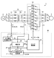
- FIG. 1 is a diagram illustrating a configuration example of a matrix converter according to the first embodiment.
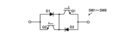
- FIG. 2 is a diagram illustrating an example of the bidirectional switch illustrated in FIG. 1.
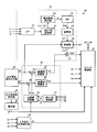
- FIG. 3 is a diagram illustrating a configuration example of a control unit of the matrix converter according to the first embodiment.
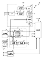
- FIG. 4 is a diagram illustrating a configuration example of a control unit of the matrix converter according to the second embodiment.
- FIG. 5 is a diagram illustrating a configuration example of a control unit of the matrix converter according to the third embodiment.
- FIG. 6 is a diagram illustrating a configuration example of a control unit of the matrix converter according to the fourth embodiment.
- FIG. 7 is a diagram illustrating a configuration example of a control unit of the matrix converter according to the fifth embodiment.
- FIG. 1 is a diagram illustrating a configuration example of a matrix converter according to the first embodiment.
- the matrix converter 1 according to the first embodiment includes input terminals Tr, Ts, Tt and output terminals Tu, Tv, Tw.
- Each phase of the three-phase AC power supply 2 is connected to the input terminals Tr, Ts, Tt, and each phase of the AC load 3 is connected to the output terminals Tu, Tv, Tw.
- the matrix converter 1 directly converts the AC power input from the three-phase AC power source 2 into AC power having a predetermined voltage and frequency and outputs the AC power to the AC load 3.
- the three-phase AC power source 2 is, for example, power supply equipment or an AC generator that transforms and supplies the voltage of the power system
- the AC load 3 is, for example, an AC motor.
- the matrix converter 1 can also perform power conversion from the AC load 3 side to the three-phase AC power source 2 side.
- the matrix converter 1 includes a power conversion unit 10, an input voltage detection unit 11, an input filter 12, an input current detection unit 13, an output current detection unit 14, and a control unit 20. .
- the power conversion unit 10 includes a plurality of bidirectional switches SW1 to SW9 that connect each phase of the three-phase AC power source 2 and each phase of the AC load 3.
- the bidirectional switches SW1 to SW3 connect the R phase, S phase, T phase of the three-phase AC power source 2 and the U phase of the AC load 3, respectively.
- the bidirectional switches SW4 to SW6 connect the R phase, S phase, and T phase of the three-phase AC power source 2 and the V phase of the AC load 3, respectively.
- the bidirectional switches SW7 to SW9 connect the R phase, S phase, T phase of the three-phase AC power source 2 and the W phase of the AC load 3, respectively.
- the bidirectional switches SW1 to SW9 can be configured by, for example, diodes D1 and D2 and unidirectional switching elements Q1 and Q2, as shown in FIG.
- FIG. 2 is a diagram showing an example of the bidirectional switches SW1 to SW9 shown in FIG.
- semiconductor switches such as IGBT (Insulated Gate Bipolar Transistor) are used.
- the energization direction is controlled by inputting a signal to the gate of the semiconductor switch to turn on / off each semiconductor switch.
- the bidirectional switches SW1 to SW9 are not limited to the configuration shown in FIG. 2, and may be a configuration in which switching elements in a single direction are connected in parallel in opposite directions.
- the input voltage detector 11 detects a voltage (hereinafter referred to as input voltage) input from the three-phase AC power source 2 to the matrix converter 1. Specifically, the input voltage detection unit 11 detects instantaneous values Vr, Vs, and Vt (hereinafter referred to as input voltage values Vr, Vs, and Vt) of the phase voltages of the three-phase AC power supply 2.
- the input voltage detection unit 11 is not limited to that shown in FIG. 1, but detects the value of the line voltage for two phases of the input phase, and the input voltage based on the value of the line voltage.
- the input voltage may be detected by using a configuration for calculating the values Vr, Vs, and Vt.
- the input filter 12 includes a reactor unit 12a and a capacitor unit 12b, and removes harmonics caused by switching of the bidirectional switches SW1 to SW9.
- Reactor unit 12 a includes three reactors provided between each of the R phase, S phase, and T phase of three-phase AC power supply 2 and power conversion unit 10.
- Capacitor portion 12b has three capacitors that are respectively arranged between the R phase and the S phase, between the S phase and the T phase, and between the T phase and the R phase.
- the capacitor unit 12b has a delta connection configuration, but may have a star connection configuration. That is, the capacitor unit 12b may have a configuration in which capacitors are respectively connected between the R phase, the S phase, the T phase, and the neutral point.
- the input current detection unit 13 detects a current flowing between the input filter 12 and the power conversion unit 10. Specifically, the input current detection unit 13 includes instantaneous values Ir, Is, It (hereinafter, referred to as current values) flowing between the R phase, the S phase, and the T phase of the three-phase AC power supply 2 and the power conversion unit 10. Input current values Ir, Is, and It) are detected.
- the input current detection unit 13 is a current sensor that detects a current by using, for example, a Hall element that is a magnetoelectric conversion element.
- the output current detection unit 14 detects a current flowing between the power conversion unit 10 and the AC load 3. Specifically, the output current detection unit 14 includes instantaneous values Iu, Iv, and Iw (hereinafter referred to as output currents) of currents flowing between the power conversion unit 10 and each of the U phase, V phase, and W phase of the AC load 3. Values Iu, Iv, and Iw).
- the output current detection unit 14 is a current sensor that detects a current by using, for example, a Hall element that is a magnetoelectric conversion element.
- the control unit 20 includes an output voltage command generation unit 31, a correction unit 32, a switch drive unit 33, and an input voltage phase detection unit 22.
- the control unit 20 generates drive signals S1 to S9 based on the detection results of the input voltage detection unit 11, the input current detection unit 13, and the output current detection unit 14, and the bidirectional switches SW1 to SW1 of the power conversion unit 10. SW9 is controlled.
- the drive signals S1 to S9 are, for example, PWM signals.
- the output voltage command generator 31 supplies the AC load 3.
- An output voltage command V * that defines the output voltage is generated and output to the correction unit 32.
- the correction unit 32 extracts a vibration component of the input current based on the input current values Ir, Is, It detected by the input current detection unit 13, and then multiplies the value of the vibration component of the input current by a predetermined coefficient. As a result, the output power correction value ⁇ P * is calculated.
- the correction unit 32 calculates the voltage correction value ⁇ V * by dividing the output power correction value ⁇ P * by the output current command I * . Then, the correction unit 32 obtains the output voltage command V1 * by adding the voltage correction value ⁇ V * to the output voltage command V * output from the output voltage command generation unit 31.
- Output voltage command V1 * which is a correction result by the correction unit 32, is output to the switch drive unit 33.
- Output voltage command V1 * is for the voltage correction value [Delta] V * with respect to the output voltage command V * is added, the output voltage to which the voltage is superposed in accordance with the vibration component of the input voltage is output from the power conversion unit 10 Is done.
- the matrix converter 1 can reduce the distortion of the input current even when the input voltage is distorted.
- the reduction of the input current distortion will be further described.
- the distortion of the input voltage occurs when the vibration component is superimposed on the fundamental component of the input voltage.
- Possible causes of the distortion of the input voltage include, for example, poor quality of the three-phase AC power supply 2 or superposition of fifth and seventh harmonics generated due to a large power supply impedance.
- control unit 20 can maintain the waveform of the output voltage and the output current in a sine wave by using, for example, vector control.
- the power P o is constant.
- the input / output active power can be regarded as equal.
- the input active power P i , the output active power P o , the input reactive power Q i, and the output reactive power Q o can be expressed by the following equation (1).
- the subscript “i” represents an input variable
- the subscript “o” represents an output variable.
- control unit 20 controls the power factor of the input voltage with respect to the fundamental wave to coincide with the command value, and the following equation (2) is established for the d-axis component and the q-axis component on the input side. This is the same even when the input voltage is distorted.
- the amplitude value Ia of the input current can be obtained by the following equation (3).
- the output voltage waveform and the output current waveform are kept in a sine wave shape with few harmonics by the voltage output based on the instantaneous value detection result of the normal input voltage, the current control function, etc., so the output active power Po is constant.
- the input active power P i is also constant. If there is distortion in this case the input voltage Vq i, in order to keep the effective input power P i constant, the input current is distorted according to distortion of the input voltage Vq i. More specifically, the above equation (2) is established by the control unit 20, but the amplitude value Ia of the input current is not constant.
- the control unit 20 obtains the voltage correction value ⁇ V * corresponding to the vibration component of the input power from the vibration component of the input current, and uses the output voltage obtained by adding the voltage correction value ⁇ V * as the power conversion unit. 10 and a vibration component corresponding to the vibration component of the input power is added to the output power. As a result, the control unit 20 reduces distortion of the input current by generating distortion in the output voltage.
- the output voltage superimposed with the vibration component corresponding to the vibration component of the input voltage is output from the power conversion unit 10 to reduce the distortion of the input current. I have to.
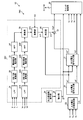
- FIG. 3 is a diagram illustrating a configuration example of the control unit 20 of the matrix converter 1 according to the first embodiment.
- the AC load 3 is an AC motor
- the AC load 3 is not limited to the motor.
- the control unit 20 of the matrix converter 1 includes an input voltage phase detection unit 22, an output frequency command unit 24, an integrator 26, an output current command generation unit 30, and an output voltage command generation unit 31. And a correction unit 32 and a switch drive unit 33.
- the input voltage phase detector 22 calculates the input voltage phase ⁇ i based on the input voltage values Vr, Vs, Vt detected by the input voltage detector 11.
- the input voltage phase detection unit 22 has, for example, a PLL (Phase Locked Loop). By reducing the loop gain built in the PLL, it is possible to reduce the sensitivity of the input voltage phase ⁇ i output from the input voltage phase detector 22 to fluctuations in the input voltage. As a result, the input voltage phase ⁇ i output from the input voltage phase detector becomes substantially equal to the phase of the fundamental wave of the input voltage.
- PLL Phase Locked Loop
- the output frequency command unit 24 determines an output frequency command that is a frequency command for the output voltage. For example, when the AC load 3 is a synchronous motor, the output frequency command unit 24 uses the frequency command converted from the speed command as an output frequency command. When the AC load 3 is an induction motor, the output frequency command unit 24 uses a known induction motor. The output frequency command is determined by the electric motor vector control law.
- the integrator 26 converts the output frequency command into an output phase command ⁇ * by integrating the output frequency command output from the output frequency command unit 24.
- the output current command generation unit 30 generates a q-axis current command Iq * and a d-axis current command Id * .
- the q-axis current command Iq * is a q-axis component of the output current command I *
- the d-axis current command Id * is a d-axis component of the output current command I * .
- the output current command I * is generated based on, for example, a speed command, a torque command, an excitation command, or the like.
- the output voltage command generator 31 generates a q-axis voltage command Vq * and a d-axis voltage command Vd * based on the q-axis current command Iq * and the d-axis current command Id * output from the output current command generator 30. .
- the q-axis voltage command Vq * is a q-axis component of the output voltage command V *
- the d-axis voltage command Vd * is a d-axis component of the output voltage command V * .
- the output voltage command generation unit 31 includes a three-phase / two-phase converter 41, a dq coordinate converter 42, a q-axis current deviation calculator 43, a d-axis current deviation calculator 44, and a q-axis current regulator 45. And a d-axis current regulator 46.
- the three-phase / two-phase converter 41 converts the output current values Iu, Iv, and Iw into two orthogonal ⁇ components on a fixed coordinate, and the ⁇ -axis current value I ⁇ and the ⁇ -axis current value I ⁇ . Is obtained as a fixed coordinate current vector I ⁇ .
- the dq coordinate converter 42 uses the output phase command ⁇ * output from the integrator 26, and the dq component of the dq coordinate system, which is a two-axis orthogonal coordinate system that rotates in synchronization with the frequency of the output voltage command described above.
- the fixed coordinate current vector I ⁇ is converted into
- the dq coordinate converter 42 uses the rotation coordinate system current vector Idq () with the q-axis current value Iq that is the current value in the q-axis direction and the d-axis current value Id that is the current value in the d-axis direction as vector components. Id, Iq).
- the q-axis current deviation calculator 43 calculates a q-axis current deviation that is a deviation between the q-axis current command Iq * and the q-axis current value Iq, and outputs it to the q-axis current regulator 45.
- the q-axis current regulator 45 performs, for example, proportional-integral control (hereinafter referred to as PI control), so that the deviation between the q-axis current command Iq * and the q-axis current value Iq becomes zero.
- PI control proportional-integral control
- the d-axis current deviation calculator 44 calculates a d-axis current deviation, which is a deviation between the d-axis current command Id * and the d-axis current value Id, and outputs it to the d-axis current regulator 46.
- the d-axis current regulator 46 adjusts the d-axis voltage command Vd * so that the deviation between the d-axis current command Id * and the d-axis current value Id becomes zero by performing PI control, for example, and performs switch driving. To the unit 33.
- the output voltage command generator 31 may further include a non-interference calculator that is not shown.
- This non-interference calculator obtains an output frequency command from the output frequency command unit 24, and from the output of the q-axis current adjuster 45, the product of the output frequency command and the d-axis current command Id * or the d-axis current value Id. The proportional voltage is subtracted to obtain a q-axis voltage command Vq * . Further, the non-interference computing unit adds a voltage proportional to the product of the output frequency command and the q-axis current command Iq * or the q-axis current value Iq to the output of the d-axis current adjuster 46 to obtain the d-axis voltage command Vd. *
- the correction unit 32 includes a low-pass filter (LPF) 51, a three-phase / two-phase converter 52, a current amplitude detector 53, a high-pass filter (HPF) 54, a multiplier 55, a divider 56, and an adder. 57.
- the LPF 51, the three-phase / two-phase converter 52, the current amplitude detector 53, the HPF 54, and the multiplier 55 correspond to an example of a first arithmetic unit
- the divider 56 corresponds to an example of a second arithmetic unit.
- LPF51 removes the high frequency component accompanying switching of the power converter 10 from input electric current value Ir, Is, It.
- the three-phase / two-phase converter 52 converts the input current values Ir, Is, It from which the high-frequency components have been removed by the LPF 51 into two orthogonal ⁇ components on fixed coordinates, and a current value I ⁇ 1 in the ⁇ -axis direction. And a current value I ⁇ 1 in the ⁇ -axis direction are obtained.
- the current amplitude detector 53 detects the amplitude value Ia of the input current by performing calculation according to the following equation (4) from the current value I ⁇ 1 and the current value I ⁇ 1.
- the HPF 54 removes the fundamental wave component of the input current from the amplitude value Ia of the input current output from the current amplitude detector 53 and extracts the vibration component ⁇ Ia of the input current.
- the multiplier 55 multiplies the vibration component ⁇ Ia of the input current extracted by the HPF 54 by the coefficient K1 to obtain the output power correction value ⁇ P.
- the coefficient K1 can be set from the outside to a value according to the use application and installation environment of the matrix converter 1. For example, the coefficient K1 can be set so that the output power correction value ⁇ P substantially matches the vibration component of the input power, The coefficient K1 can also be set so that the output power correction value ⁇ P becomes a predetermined ratio (for example, 50%) of the vibration component of the input power.
- the cut-off frequency f LPF of the LPF 51 and the cut-off frequency f HPF of the HPF 54 are determined so as to satisfy the relationship of f LPF > f HPF . Thereby, only the high frequency component resulting from the distortion of an input voltage from which the high frequency component by switching of the power converter 10 was removed can be obtained as the output of the HPF 54.
- the output power correction value ⁇ P calculated by the multiplier 55 is input to the divider 56.
- the adder 57 calculates the q-axis voltage command Vq1 * by adding the voltage correction value ⁇ V * output from the divider 56 to the q-axis voltage command Vq * output from the output voltage command generation unit 31.
- the adder 57 outputs the q-axis voltage command Vq1 * to the switch driving unit 33.
- the switch drive unit 33 drives the bidirectional switches SW1 to SW9 based on the q-axis voltage command Vq1 * output from the correction unit 32 and the d-axis voltage command Vd * output from the output voltage command generation unit 31. Drive signals S1 to S9 are generated.
- the switch drive unit 33 obtains the output voltage command V1 * and the output voltage phase command ⁇ a * from the following equation (5) based on the q-axis voltage command Vq1 * and the d-axis voltage command Vd * , for example. Further, the switch driving unit 33 adds the output phase command ⁇ * that is the output of the integrator 26 to the output voltage phase command ⁇ a * to obtain the phase ⁇ p.
- the switch driving unit 33 calculates the three-phase AC voltage command, that is, the output voltage command Vu for each phase of the AC load 3, from the following equation (6). * , Vv * , Vw * are obtained.
- the switch driving unit 33 uses, for example, a known matrix converter pulse width modulation method to generate power.
- Drive signals S1 to S9 for controlling the bidirectional switches SW1 to SW9 of the converter 10 are generated and output.
- a three-phase AC voltage corresponding to the output voltage commands Vu * , Vv * , Vw * is output from the power conversion unit 10, and the phase of the input current has a certain phase difference with respect to the input voltage phase ⁇ i .
- the power factor on the input side is a constant value.
- the output voltage from the power converter 10 includes the vibration component of the input power.
- the corresponding vibration component is superimposed, and the output active power Po changes.
- the vibration component corresponding to the vibration component of the input voltage is generated in the output active power P o.
- vibration component in the input active power P i is generated. Since the vibration component of the input active power P i corresponds to the vibration component of the input voltage, distortion of the input current is reduced. Therefore, by setting the coefficient K1 so that the vibration component of the output power substantially matches the vibration component of the input voltage, the input current can be kept substantially sinusoidal.
- FIG. 4 is a diagram illustrating a configuration example of a control unit of the matrix converter according to the second embodiment.
- the correction unit 32A corrects the d-axis voltage command Vd * with the voltage correction value ⁇ V * .
- the correction unit 32A includes an LPF 51, a three-phase / two-phase converter 52, a current amplitude detector 53, an HPF 54, a multiplier 55, a divider 56A, and an adder 57A.
- the LPF 51, the three-phase / two-phase converter 52, the current amplitude detector 53, the HPF 54, and the multiplier 55 have the same configuration as that of the correction unit 32.
- the adder 57A calculates the d-axis voltage command Vd1 * by adding the voltage correction value ⁇ V * output from the divider 56A to the d-axis voltage command Vd * output from the output voltage command generation unit 31. Then, the adder 57A outputs the d-axis voltage command Vd1 * to the switch driving unit 33.
- the switch drive unit 33 generates drive signals S1 to S9 based on the d-axis voltage command Vd1 * and the q-axis voltage command Vq * .
- the vibration component corresponding to the vibration component of the input voltage can be superimposed on the output voltage by correcting the d-axis component of the output voltage instead of correcting the q-axis component of the output voltage. Absent.
- the matrix converter 1A according to the second embodiment similarly to the matrix converter 1 according to the first embodiment, even when the input voltage is distorted, the distortion of the input current can be reduced. it can.
- FIG. 5 is a diagram illustrating a configuration example of a control unit of the matrix converter according to the third embodiment.
- the correction unit 32B In the control unit 20B of the matrix converter 1B according to the third embodiment, the correction unit 32B generates a voltage correction value according to the vibration component of the input voltage.
- the correction unit 32B includes an LPF 51B, a three-phase / two-phase converter 52B, a voltage amplitude detector 53B, an HPF 54B, a multiplier 55B, a divider 56, an adder 57, And a phase advance filter 58.
- LPF 51B removes high frequency components accompanying switching of the power conversion unit 10 from the input voltage values Vr, Vs, and Vt.
- the three-phase / two-phase converter 52B converts the input voltage values Vr, Vs, Vt, from which the high-frequency component has been removed by the LPF 51B, into two orthogonal ⁇ components on a fixed coordinate, and a voltage value V ⁇ in the ⁇ -axis direction. And a voltage value V ⁇ in the ⁇ -axis direction are obtained.
- the voltage amplitude detector 53B detects the amplitude value Va of the input voltage by performing calculation according to the following equation (7) from the voltage value V ⁇ and the voltage value V ⁇ .
- the HPF 54B removes the fundamental component of the input voltage from the amplitude value Va of the input voltage output from the voltage amplitude detector 53B, and extracts the vibration component ⁇ Va of the input voltage.
- the phase advance filter 58 advances the phase of the vibration component ⁇ Va of the input voltage extracted by the HPF 54B by 90 degrees and outputs the result to the multiplier 55B. By advancing the phase of the vibration component ⁇ Va of the input voltage by 90 degrees, the vibration component ⁇ Va of the input voltage is converted into a value corresponding to the vibration component of the input current.
- the multiplier 55B multiplies the vibration component ⁇ Va of the input voltage whose phase is advanced by 90 degrees by the phase advance filter 58 by the coefficient K2 to obtain the output power correction value ⁇ P.
- the coefficient K2 is set so that the output power correction value ⁇ P substantially matches the vibration component of the input power.
- the coefficient K2 can be set from the outside to a value according to the use application and installation environment of the matrix converter 1B so that the output power correction value ⁇ P becomes a predetermined ratio (for example, 50%) of the vibration component of the input power. It is also possible to set the coefficient K2.
- the output power correction value ⁇ P calculated by the multiplier 55B is input to the divider 56.
- the adder 57 calculates the q-axis voltage command Vq1 * by adding the voltage correction value ⁇ V * output from the divider 56 to the q-axis voltage command Vq * output from the output voltage command generation unit 31.
- the adder 57 outputs the q-axis voltage command Vq1 * to the switch driving unit 33.
- the output power correction value ⁇ P is calculated based on the vibration component of the input voltage, and the voltage correction value ⁇ V * is calculated from the output power correction value ⁇ P.
- the matrix converter 1B according to the third embodiment similarly to the matrix converter 1 according to the first embodiment, it is possible to reduce the distortion of the input current even when the input voltage is distorted. .
- the coefficient K2 so that the output power correction value ⁇ P substantially matches the vibration component of the input power, it is possible to keep the input current in a substantially sine wave.
- the voltage correction value ⁇ V * is added to the q-axis voltage command Vq * .
- the d-axis voltage command Vd * is added to the d-axis voltage command Vd * .
- the voltage correction value ⁇ V * may be added.
- FIG. 6 is a diagram illustrating a configuration example of a control unit of the matrix converter according to the fourth embodiment.
- the correction unit 32C generates a voltage correction value according to the vibration component of the input current and the vibration component of the input voltage.
- the correction unit 32C includes LPFs 51 and 51B, three-phase / two-phase converters 52 and 52B, a current amplitude detector 53, a voltage amplitude detector 53B, HPFs 54 and 54B, and a multiplier. 59, 55C, a divider 56, and an adder 57.
- the amplitude of the input current is extracted by the LPF 51, the 3-phase / 2-phase converter 52, the current amplitude detector 53, and the HPF 54, and the LPF 51B, the 3-phase / 2-phase converter 52B, the voltage amplitude detector 53B, and the HPF 54B. Is used to extract the amplitude of the input voltage. Note that, by making the cut-off frequencies of the HPFs 54 and 54B the same, the voltage correction value ⁇ V can be accurately generated in the correction unit 32C.
- the multiplier 59 multiplies the vibration component of the input current extracted by the HPF 54 and the vibration component of the input voltage extracted by the HFP 54B. As a result, the vibration component of the input power can be extracted.
- the multiplier 55C multiplies the multiplication result of the multiplier 59 by the coefficient K3.
- the coefficient K3 can be set from the outside to a value according to the use application and installation environment of the matrix converter 1C. For example, when the output power correction value ⁇ P is substantially matched with the vibration component of the input power, for example, the coefficient K3 Is set to “1”. When the output power correction value ⁇ P is set to a predetermined ratio (for example, 50%) of the vibration component of the input power, a value corresponding to the ratio is set as the coefficient K3.
- a predetermined ratio for example, 50%
- the adder 57 calculates the q-axis voltage command Vq1 * by adding the voltage correction value ⁇ V * output from the divider 56 to the q-axis voltage command Vq * output from the output voltage command generation unit 31.
- the adder 57 outputs the q-axis voltage command Vq1 * to the switch driving unit 33.
- the output power correction value ⁇ P corresponding to the vibration component of the input current and the vibration component of the input voltage is calculated, and the voltage correction value ⁇ V is calculated from the output power correction value ⁇ P. * Is calculated. Therefore, the matrix converter 1C can superimpose the vibration component corresponding to the vibration component of the input voltage on the output voltage, as in the case of the matrix converters 1, 1A, 1B. However, the distortion of the input current can be reduced. For example, the input current can be kept substantially sinusoidal by setting the coefficient K3 to “1”.
- the voltage correction value ⁇ V * is added to the q-axis voltage command Vq * .
- the d-axis voltage command Vd * is added to the d-axis voltage command Vd * .
- the voltage correction value ⁇ V * may be added.
- FIG. 7 is a diagram illustrating a configuration example of a control unit of the matrix converter according to the fifth embodiment.
- the coefficient K4 of the multiplier 55D can be adjusted by the correction unit 32D.
- the correction unit 32D includes an absolute value calculator 70, a moving average calculator 71, a subtractor 72, and a PI controller 73 in addition to the configuration of the correction unit 32 according to the first embodiment.
- the absolute value calculator 70 calculates the absolute value
- the moving average calculator 71 obtains the moving average of the absolute value
- the subtractor 72 calculates the difference between the command value Ia * of the vibration component of the input current input from the outside and the moving average of the absolute value
- the PI controller 73 performs, for example, PI control so that the deviation between the command value Ia * of the vibration component of the input current and the moving average of the absolute value
- the multiplier 55D is an arithmetic unit corresponding to the multiplier 55, and outputs the result obtained by multiplying the vibration component ⁇ Ia of the input current by the coefficient K4 to the divider 56 as the output power correction value ⁇ P. Therefore, in the matrix converter 1D according to the fifth embodiment, the vibration component ⁇ Ia of the input current can be set to a value corresponding to the command value Ia * , and thereby distortion of the input current can be reduced.
Landscapes
- Engineering & Computer Science (AREA)
- Power Engineering (AREA)
- Ac-Ac Conversion (AREA)
Description
図1は、第1の実施形態に係るマトリクスコンバータの構成例を示す図である。図1に示すように、第1の実施形態に係るマトリクスコンバータ1は、入力端子Tr、Ts、Ttおよび出力端子Tu、Tv、Twを備える。入力端子Tr、Ts、Ttに3相交流電源2の各相が接続され、出力端子Tu、Tv、Twに交流負荷3の各相が接続される。






次に、第2の実施形態に係るマトリクスコンバータの制御部について説明する。第1の実施形態に係る制御部20では、q軸電圧指令Vq*に対して電圧補正値ΔV*を加算することとしたが、第2の実施形態に係る制御部では、d軸電圧指令Vd*に対して電圧補正値ΔV*を加算する。なお、以下においては、第1の実施形態と異なる部分を主として説明し、共通する部分については同一符号を付し適宜説明を省略する。
次に、第3の実施形態に係るマトリクスコンバータの制御部について説明する。第1および第2の実施形態に係る制御部20、20Aでは、入力電流の振動成分に応じた電圧補正値ΔV*を算出することとしたが、第3の実施形態に係る制御部では、入力電圧の振動成分に応じた電圧補正値を算出する。なお、以下においては、第1および第2の実施形態と異なる部分を主として説明し、共通する部分については同一符号を付し適宜説明を省略する。

次に、第4の実施形態に係るマトリクスコンバータの制御部について説明する。第1~第3の実施形態に係る制御部20、20A、20Bでは、入力電流または入力電圧の振動成分に応じた電圧補正値ΔV*を算出することとした。一方、第4の実施形態に係る制御部では、入力電流の振動成分および入力電圧の振動成分に応じた電圧補正値ΔV*を算出する。以下においては、第1の実施形態と異なる部分を主として説明し、共通する部分については同一符号を付し適宜説明を省略する。
次に、第5の実施形態に係るマトリクスコンバータの制御部について説明する。第1~第4の実施形態に係る制御部20、20A~20Cでは、乗算器55、55B、55Cにおいて、係数K1~K3を外部から設定可能とした。一方、第5の実施形態に係る制御部では、入力電流の振動成分の指令値を設定可能としている。なお、以下においては、第1の実施形態と異なる部分を主として説明し、共通する部分については同一符号を付し適宜説明を省略する。
2 3相交流電源
3 交流負荷
10 電力変換部
11 入力電圧検出部
12 入力フィルタ
13 入力電流検出部
14 出力電流検出部
20、20A~20D 制御部
30 出力電流指令生成部
31 出力電圧指令生成部
32、32A~32D 補正部
33 スイッチ駆動部
51、51B LPF
52、52B 3相/2相変換部
53 電流振幅検出器
53B 電圧振幅検出器
54、54B HPF
55、55B~55D、59 乗算器
56、56A 除算器
57、57A 加算器
58 進相フィルタ
Claims (10)
- 交流電源と交流負荷との間に配置される複数の双方向スイッチと、
前記複数の双方向スイッチを制御し、前記交流電源からの入力電力を直接電力変換して前記交流負荷へ出力する制御部と、を備え、
前記制御部は、
前記交流負荷への出力電圧を規定する出力電圧指令を生成する出力電圧指令生成部と、
前記交流電源からの入力電流および/または入力電圧の振動成分に基づいて、前記出力電圧指令を補正する補正部と、
前記補正部によって補正された前記出力電圧指令に基づいて前記複数の双方向スイッチを制御するスイッチ駆動部と、を備える
ことを特徴とするマトリクスコンバータ。 - 前記補正部は、
前記入力電流および/または入力電圧の振動成分に基づき、出力電力補正値を算出する第1演算器と、
前記出力電力補正値に応じた電圧補正値を算出する第2演算器と、
前記第2演算器によって生成された前記電圧補正値を前記出力電圧指令に加算することによって、前記出力電圧指令を補正する加算器と、を備える
ことを特徴とする請求項1に記載のマトリクスコンバータ。 - 前記第2演算器は、
前記第1演算器によって演算された前記出力電力補正値を、前記交流負荷への出力電流を規定する出力電流指令で除算することによって、前記電圧補正値を算出する
ことを特徴とする請求項2に記載のマトリクスコンバータ。 - 前記第1演算器は、
前記入力電流の振動成分に所定の係数を乗算して前記出力電力補正値を算出する
ことを特徴とする請求項3に記載のマトリクスコンバータ。 - 前記第1演算器は、
前記入力電圧の振動成分の位相を進ませ、所定の係数を乗算して前記出力電力補正値を算出する
ことを特徴とする請求項3に記載のマトリクスコンバータ。 - 前記第1演算器は、
前記入力電流の振動成分と前記入力電圧の振動成分とを乗算して前記出力電力補正値を算出する
ことを特徴とする請求項3に記載のマトリクスコンバータ。 - 前記第1演算器は、
前記入力電流の振動成分と前記入力電圧の振動成分との乗算結果に所定の係数を乗算して前記出力電力補正値を算出する
ことを特徴とする請求項6に記載のマトリクスコンバータ。 - 前記第1演算器は、
前記所定の係数を外部から設定可能である
ことを特徴とする請求項4、5、7のいずれか1項に記載のマトリクスコンバータ。 - 前記所定の係数を調整する調整部を備える
ことを特徴とする請求項4、5、7のいずれか1項に記載のマトリクスコンバータ。 - 前記出力電圧指令生成部は、
前記出力電圧指令として、前記出力電圧の周波数に同期して回転する2軸直交座標系のdq軸上のq軸電圧指令およびd軸電圧指令を生成し、
前記補正部は、
前記交流電源からの入力電流および/または入力電圧の振動成分に基づいて、前記q軸電圧指令または前記d軸電圧指令を補正する
ことを特徴とする請求項1~7のいずれか1項に記載のマトリクスコンバータ。
Priority Applications (5)
| Application Number | Priority Date | Filing Date | Title |
|---|---|---|---|
| PCT/JP2012/069483 WO2014020703A1 (ja) | 2012-07-31 | 2012-07-31 | マトリクスコンバータ |
| JP2014527874A JP5915751B2 (ja) | 2012-07-31 | 2012-07-31 | マトリクスコンバータ |
| KR20157002433A KR20150036263A (ko) | 2012-07-31 | 2012-07-31 | 매트릭스 컨버터 |
| CN201280074503.2A CN104428986A (zh) | 2012-07-31 | 2012-07-31 | 矩阵变换器 |
| US14/604,756 US20150137779A1 (en) | 2012-07-31 | 2015-01-26 | Matrix converter and method for controlling matrix converter |
Applications Claiming Priority (1)
| Application Number | Priority Date | Filing Date | Title |
|---|---|---|---|
| PCT/JP2012/069483 WO2014020703A1 (ja) | 2012-07-31 | 2012-07-31 | マトリクスコンバータ |
Related Child Applications (1)
| Application Number | Title | Priority Date | Filing Date |
|---|---|---|---|
| US14/604,756 Continuation US20150137779A1 (en) | 2012-07-31 | 2015-01-26 | Matrix converter and method for controlling matrix converter |
Publications (1)
| Publication Number | Publication Date |
|---|---|
| WO2014020703A1 true WO2014020703A1 (ja) | 2014-02-06 |
Family
ID=50027434
Family Applications (1)
| Application Number | Title | Priority Date | Filing Date |
|---|---|---|---|
| PCT/JP2012/069483 Ceased WO2014020703A1 (ja) | 2012-07-31 | 2012-07-31 | マトリクスコンバータ |
Country Status (5)
| Country | Link |
|---|---|
| US (1) | US20150137779A1 (ja) |
| JP (1) | JP5915751B2 (ja) |
| KR (1) | KR20150036263A (ja) |
| CN (1) | CN104428986A (ja) |
| WO (1) | WO2014020703A1 (ja) |
Cited By (5)
| Publication number | Priority date | Publication date | Assignee | Title |
|---|---|---|---|---|
| JP2015012729A (ja) * | 2013-06-28 | 2015-01-19 | 株式会社安川電機 | マトリクスコンバータ |
| CN104485852A (zh) * | 2014-11-12 | 2015-04-01 | 江苏大学 | 一种基于矩阵变换器的三极磁轴承运行控制系统及方法 |
| CN104638939A (zh) * | 2015-01-29 | 2015-05-20 | 南京航空航天大学 | 一种抑制矩阵变换器输入侧振荡的控制方法 |
| JP2019115120A (ja) * | 2017-12-21 | 2019-07-11 | 株式会社富士通ゼネラル | マトリックスコンバータおよび電力変換システム |
| JP2021118625A (ja) * | 2020-01-27 | 2021-08-10 | 株式会社富士通ゼネラル | センサレスモータ制御装置 |
Families Citing this family (9)
| Publication number | Priority date | Publication date | Assignee | Title |
|---|---|---|---|---|
| EP2728729A2 (en) * | 2012-10-30 | 2014-05-07 | Kabushiki Kaisha Yaskawa Denki | Matrix converter |
| WO2014174667A1 (ja) | 2013-04-26 | 2014-10-30 | 富士電機株式会社 | 共振抑制装置 |
| US9316701B1 (en) * | 2014-05-06 | 2016-04-19 | The Florida State University Research Foundation, Inc. | Real-time small-signal stability assessment of power electronic-based components in contemporary power systems |
| FR3042075B1 (fr) * | 2015-10-06 | 2018-10-12 | Universite De Poitiers | Determination d'une pollution harmonique sur un reseau de distribution d'energie electrique |
| US10587214B1 (en) * | 2019-03-22 | 2020-03-10 | Hamilton Sundstrand Corporation | Matrix converter operation in current control mode with regulation of output voltage vector |
| CN111426877B (zh) * | 2020-06-11 | 2020-11-03 | 四川明星电力股份有限公司 | 电力保护装置核查方法及系统 |
| JP7127671B2 (ja) * | 2020-08-31 | 2022-08-30 | 株式会社安川電機 | 電力変換装置及び電力変換方法 |
| JP7127672B2 (ja) | 2020-08-31 | 2022-08-30 | 株式会社安川電機 | 電力変換装置及び電力変換方法 |
| CN114738384B (zh) * | 2022-03-21 | 2024-07-09 | 中国舰船研究设计中心 | 电励磁式三极磁悬浮轴承的驱动装置、控制装置及方法 |
Citations (4)
| Publication number | Priority date | Publication date | Assignee | Title |
|---|---|---|---|---|
| JP2002354815A (ja) * | 2001-05-29 | 2002-12-06 | Yaskawa Electric Corp | Pwmサイクロコンバータの入力電流制御方法とpwmサイクロコンバータ装置 |
| JP2004007929A (ja) * | 2002-06-03 | 2004-01-08 | Fuji Electric Holdings Co Ltd | 交流/交流直接形電力変換装置の出力電圧補償装置 |
| JP2006262560A (ja) * | 2005-03-15 | 2006-09-28 | Nagaoka Univ Of Technology | 交流交流直接電力変換器の制御装置 |
| JP2007306649A (ja) * | 2006-05-09 | 2007-11-22 | Yaskawa Electric Corp | 直列多重マトリクスコンバータ |
Family Cites Families (14)
| Publication number | Priority date | Publication date | Assignee | Title |
|---|---|---|---|---|
| US6058028A (en) * | 1999-05-12 | 2000-05-02 | Otis Elevator Company | Control of a DC matrix converter |
| US6839249B2 (en) * | 2001-01-10 | 2005-01-04 | Honeywell International Inc. | AC-to-ac power converter without a dc link capacitor |
| US6882549B2 (en) * | 2001-03-21 | 2005-04-19 | Honeywell International Inc. | Active filter for power distribution system with selectable harmonic elimination |
| US6771524B2 (en) * | 2001-12-27 | 2004-08-03 | Otis Elevator Company | Multiple PWM cycloconverter |
| US6984960B2 (en) * | 2003-08-05 | 2006-01-10 | General Motors Corporation | Methods and apparatus for current control of a three-phase voltage source inverter in the overmodulation region |
| WO2009144987A1 (ja) * | 2008-05-30 | 2009-12-03 | 株式会社安川電機 | マトリクスコンバータの制御装置及びその出力電圧発生方法 |
| JP5246508B2 (ja) * | 2009-05-28 | 2013-07-24 | アイシン・エィ・ダブリュ株式会社 | 電動機駆動装置の制御装置 |
| WO2010140650A1 (ja) * | 2009-06-04 | 2010-12-09 | ダイキン工業株式会社 | 電力変換装置 |
| US9054589B2 (en) * | 2010-05-28 | 2015-06-09 | Rockwell Automation Technologies, Inc. | Method and apparatus for detecting power converter capacitor degradation using negative sequence currents |
| EP2715922A2 (en) * | 2011-06-01 | 2014-04-09 | FH Joanneum GmbH | Inverter |
| CN103828213B (zh) * | 2011-09-26 | 2017-02-22 | 大金工业株式会社 | 电力转换器控制方法 |
| CN103036529B (zh) * | 2011-09-29 | 2017-07-07 | 株式会社大亨 | 信号处理装置、滤波器、控制电路、逆变器和转换器系统 |
| JP5996531B2 (ja) * | 2011-11-22 | 2016-09-21 | パナソニック株式会社 | 交流変換回路 |
| US9046560B2 (en) * | 2012-06-04 | 2015-06-02 | Eaton Corporation | System and method for high resistance ground fault detection and protection in power distribution systems |
-
2012
- 2012-07-31 KR KR20157002433A patent/KR20150036263A/ko not_active Ceased
- 2012-07-31 JP JP2014527874A patent/JP5915751B2/ja active Active
- 2012-07-31 CN CN201280074503.2A patent/CN104428986A/zh active Pending
- 2012-07-31 WO PCT/JP2012/069483 patent/WO2014020703A1/ja not_active Ceased
-
2015
- 2015-01-26 US US14/604,756 patent/US20150137779A1/en not_active Abandoned
Patent Citations (4)
| Publication number | Priority date | Publication date | Assignee | Title |
|---|---|---|---|---|
| JP2002354815A (ja) * | 2001-05-29 | 2002-12-06 | Yaskawa Electric Corp | Pwmサイクロコンバータの入力電流制御方法とpwmサイクロコンバータ装置 |
| JP2004007929A (ja) * | 2002-06-03 | 2004-01-08 | Fuji Electric Holdings Co Ltd | 交流/交流直接形電力変換装置の出力電圧補償装置 |
| JP2006262560A (ja) * | 2005-03-15 | 2006-09-28 | Nagaoka Univ Of Technology | 交流交流直接電力変換器の制御装置 |
| JP2007306649A (ja) * | 2006-05-09 | 2007-11-22 | Yaskawa Electric Corp | 直列多重マトリクスコンバータ |
Cited By (8)
| Publication number | Priority date | Publication date | Assignee | Title |
|---|---|---|---|---|
| JP2015012729A (ja) * | 2013-06-28 | 2015-01-19 | 株式会社安川電機 | マトリクスコンバータ |
| CN104485852A (zh) * | 2014-11-12 | 2015-04-01 | 江苏大学 | 一种基于矩阵变换器的三极磁轴承运行控制系统及方法 |
| CN104485852B (zh) * | 2014-11-12 | 2016-06-22 | 江苏大学 | 一种基于矩阵变换器的三极磁轴承运行控制系统及方法 |
| CN104638939A (zh) * | 2015-01-29 | 2015-05-20 | 南京航空航天大学 | 一种抑制矩阵变换器输入侧振荡的控制方法 |
| JP2019115120A (ja) * | 2017-12-21 | 2019-07-11 | 株式会社富士通ゼネラル | マトリックスコンバータおよび電力変換システム |
| JP7027875B2 (ja) | 2017-12-21 | 2022-03-02 | 株式会社富士通ゼネラル | マトリックスコンバータおよび電力変換システム |
| JP2021118625A (ja) * | 2020-01-27 | 2021-08-10 | 株式会社富士通ゼネラル | センサレスモータ制御装置 |
| JP7363524B2 (ja) | 2020-01-27 | 2023-10-18 | 株式会社富士通ゼネラル | センサレスモータ制御装置 |
Also Published As
| Publication number | Publication date |
|---|---|
| JPWO2014020703A1 (ja) | 2016-07-11 |
| JP5915751B2 (ja) | 2016-05-11 |
| US20150137779A1 (en) | 2015-05-21 |
| CN104428986A (zh) | 2015-03-18 |
| KR20150036263A (ko) | 2015-04-07 |
Similar Documents
| Publication | Publication Date | Title |
|---|---|---|
| JP5915751B2 (ja) | マトリクスコンバータ | |
| US9219424B2 (en) | Matrix converter | |
| US8269441B2 (en) | Motor control apparatus | |
| TWI654827B (zh) | 換流器控制裝置及馬達驅動系統 | |
| JP3722048B2 (ja) | モーター制御装置 | |
| CN108123653B (zh) | 马达控制系统的自适应脉宽调制 | |
| US8878471B2 (en) | Control apparatus for electric rotary machine | |
| CN109952701B (zh) | 电动机控制装置及具备该电动机控制装置的电动助力转向控制装置 | |
| CN101299590A (zh) | 脉冲宽度调制逆变器的电流调节器的抗积分饱和控制 | |
| US6927551B2 (en) | Motor control apparatus and motor control method | |
| JP5968564B2 (ja) | 電力変換装置 | |
| US10903755B2 (en) | Power conversion device | |
| JP6374037B2 (ja) | モータ制御装置 | |
| WO2018131093A1 (ja) | モータ制御装置 | |
| WO2016143121A1 (ja) | 交流回転機の制御装置および電動パワーステアリングの制御装置 | |
| CN112448644B (zh) | 电动机控制器与电动机控制方法 | |
| CN101427455B (zh) | 电力变换器的控制装置 | |
| US8749184B2 (en) | Control apparatus for electric motor | |
| JP4722002B2 (ja) | Pwmインバータ制御装置及びpwmインバータ制御方法並びに冷凍空調装置 | |
| JP2012039716A (ja) | モータ制御装置及びモータ制御方法 | |
| WO2015005016A1 (ja) | インバータの制御装置及びインバータの制御方法 | |
| JP2013172550A (ja) | モータ制御装置及びモータの3相電圧指令生成方法 | |
| JP2006121855A (ja) | 交流モータ制御装置 | |
| JP5640452B2 (ja) | 電力変換器の制御装置 | |
| JP2005223991A (ja) | インバータ制御装置 |
Legal Events
| Date | Code | Title | Description |
|---|---|---|---|
| 121 | Ep: the epo has been informed by wipo that ep was designated in this application |
Ref document number: 12882400 Country of ref document: EP Kind code of ref document: A1 |
|
| ENP | Entry into the national phase |
Ref document number: 2014527874 Country of ref document: JP Kind code of ref document: A |
|
| ENP | Entry into the national phase |
Ref document number: 20157002433 Country of ref document: KR Kind code of ref document: A |
|
| NENP | Non-entry into the national phase |
Ref country code: DE |
|
| 122 | Ep: pct application non-entry in european phase |
Ref document number: 12882400 Country of ref document: EP Kind code of ref document: A1 |