WO2014010237A1 - 半導体装置の製造方法 - Google Patents
半導体装置の製造方法 Download PDFInfo
- Publication number
- WO2014010237A1 WO2014010237A1 PCT/JP2013/004255 JP2013004255W WO2014010237A1 WO 2014010237 A1 WO2014010237 A1 WO 2014010237A1 JP 2013004255 W JP2013004255 W JP 2013004255W WO 2014010237 A1 WO2014010237 A1 WO 2014010237A1
- Authority
- WO
- WIPO (PCT)
- Prior art keywords
- adhesive
- semiconductor wafer
- semiconductor
- cover film
- manufacturing
- Prior art date
- Legal status (The legal status is an assumption and is not a legal conclusion. Google has not performed a legal analysis and makes no representation as to the accuracy of the status listed.)
- Ceased
Links
Images











Classifications
-
- H—ELECTRICITY
- H10—SEMICONDUCTOR DEVICES; ELECTRIC SOLID-STATE DEVICES NOT OTHERWISE PROVIDED FOR
- H10W—GENERIC PACKAGES, INTERCONNECTIONS, CONNECTORS OR OTHER CONSTRUCTIONAL DETAILS OF DEVICES COVERED BY CLASS H10
- H10W72/00—Interconnections or connectors in packages
- H10W72/01—Manufacture or treatment
- H10W72/013—Manufacture or treatment of die-attach connectors
-
- H—ELECTRICITY
- H10—SEMICONDUCTOR DEVICES; ELECTRIC SOLID-STATE DEVICES NOT OTHERWISE PROVIDED FOR
- H10W—GENERIC PACKAGES, INTERCONNECTIONS, CONNECTORS OR OTHER CONSTRUCTIONAL DETAILS OF DEVICES COVERED BY CLASS H10
- H10W72/00—Interconnections or connectors in packages
- H10W72/30—Die-attach connectors
-
- H—ELECTRICITY
- H10—SEMICONDUCTOR DEVICES; ELECTRIC SOLID-STATE DEVICES NOT OTHERWISE PROVIDED FOR
- H10W—GENERIC PACKAGES, INTERCONNECTIONS, CONNECTORS OR OTHER CONSTRUCTIONAL DETAILS OF DEVICES COVERED BY CLASS H10
- H10W72/00—Interconnections or connectors in packages
- H10W72/071—Connecting or disconnecting
- H10W72/073—Connecting or disconnecting of die-attach connectors
-
- H—ELECTRICITY
- H10—SEMICONDUCTOR DEVICES; ELECTRIC SOLID-STATE DEVICES NOT OTHERWISE PROVIDED FOR
- H10W—GENERIC PACKAGES, INTERCONNECTIONS, CONNECTORS OR OTHER CONSTRUCTIONAL DETAILS OF DEVICES COVERED BY CLASS H10
- H10W72/00—Interconnections or connectors in packages
- H10W72/071—Connecting or disconnecting
- H10W72/073—Connecting or disconnecting of die-attach connectors
- H10W72/07331—Connecting techniques
- H10W72/07337—Connecting techniques using a polymer adhesive, e.g. an adhesive based on silicone or epoxy
- H10W72/07338—Connecting techniques using a polymer adhesive, e.g. an adhesive based on silicone or epoxy hardening the adhesive by curing, e.g. thermosetting
-
- H—ELECTRICITY
- H10—SEMICONDUCTOR DEVICES; ELECTRIC SOLID-STATE DEVICES NOT OTHERWISE PROVIDED FOR
- H10W—GENERIC PACKAGES, INTERCONNECTIONS, CONNECTORS OR OTHER CONSTRUCTIONAL DETAILS OF DEVICES COVERED BY CLASS H10
- H10W72/00—Interconnections or connectors in packages
- H10W72/071—Connecting or disconnecting
- H10W72/073—Connecting or disconnecting of die-attach connectors
- H10W72/07351—Connecting or disconnecting of die-attach connectors characterised by changes in properties of the die-attach connectors during connecting
- H10W72/07352—Connecting or disconnecting of die-attach connectors characterised by changes in properties of the die-attach connectors during connecting changes in structures or sizes
-
- H—ELECTRICITY
- H10—SEMICONDUCTOR DEVICES; ELECTRIC SOLID-STATE DEVICES NOT OTHERWISE PROVIDED FOR
- H10W—GENERIC PACKAGES, INTERCONNECTIONS, CONNECTORS OR OTHER CONSTRUCTIONAL DETAILS OF DEVICES COVERED BY CLASS H10
- H10W72/00—Interconnections or connectors in packages
- H10W72/30—Die-attach connectors
- H10W72/321—Structures or relative sizes of die-attach connectors
Definitions
- the present disclosure relates to a method for manufacturing a semiconductor device in which a semiconductor wafer is diced and cut into semiconductor chips and then the semiconductor chips are mounted on a substrate.
- Patent Document 1 describes a method of dicing a semiconductor wafer by applying an adhesive to one surface of a semiconductor wafer and inserting a dicing blade from the adhesive side.
- An object of the present disclosure is to provide a method of manufacturing a semiconductor device that can be cut by dicing so as not to entrap foreign matter even if a soft adhesive is provided on a conductor wafer.
- a method for manufacturing a semiconductor device includes preparing a semiconductor wafer, placing an adhesive at a predetermined position on one surface of the semiconductor wafer, and dicing the semiconductor wafer.
- the semiconductor wafer is divided into individual semiconductor chips, a substrate is prepared, the semiconductor chip is mounted on the substrate via the adhesive, and the adhesive is temporarily cured.
- the temporary curing of the adhesive is performed before the placement of the adhesive or after the placement of the adhesive.
- the temporary curing of the adhesive is performed before the dicing cut.
- the semiconductor wafer is diced and cut after the adhesive is hardened to some extent by the temporary curing step, it is possible to prevent the soft adhesive from being caught in the dicing blade as a foreign matter. it can. Therefore, even if a soft adhesive is provided on the semiconductor wafer, dicing can be cut so that no foreign matter is caught in the dicing blade.
- a portion of the adhesive that does not contact the semiconductor wafer may be covered with a cover film.
- the adhesive when the adhesive is disposed on one surface of the semiconductor wafer, the adhesive is covered with the cover film. For this reason, it can prevent that the coupling agent which determines adhesiveness is washed from an adhesive agent at the time of a dicing cut. That is, it is possible to prevent a decrease in the adhesive coupling agent.
- the method for manufacturing a semiconductor device may include a method in which the adhesive is not disposed on one surface of the semiconductor wafer after the placement of the adhesive and the temporary curing of the adhesive and before the dicing cut. It may further include disposing a protective material harder than the adhesive. In the dicing cut, the semiconductor wafer is diced and cut in a state where the protective material is disposed on one surface of the semiconductor wafer. In this case, since the region where the adhesive is not disposed on one surface of the semiconductor wafer is covered with the protective material, the shavings adhere to the region, or the shavings attached to the region are prevented from adhering to the adhesive. be able to. Further, since the protective material is harder than the adhesive, it is difficult for foreign matter to come out when the protective material is shaved. For this reason, the adhesion of foreign matter to the adhesive can be prevented.
- FIG. 1 is a cross-sectional view of the semiconductor device according to the first embodiment.
- FIG. 2A to FIG. 2D are diagrams showing manufacturing steps of the semiconductor device shown in FIG.
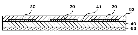
- FIG. 3 is a diagram illustrating a manufacturing process of the semiconductor device according to the second embodiment.
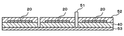
- FIG. 4 is a diagram showing how the semiconductor wafer is diced and cut from the cover film side in the second embodiment.
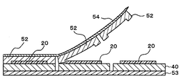
- FIG. 5 is a diagram showing a state where the cover film is peeled off from the semiconductor chip in the second embodiment.
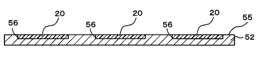
- FIG. 6 is a diagram illustrating a state in which an adhesive is disposed on the cover film in the third embodiment.
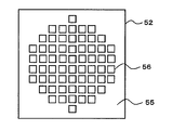
- FIG. 7 is a plan view of a cover film according to the third embodiment.
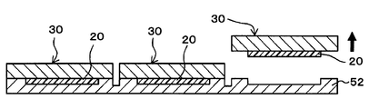
- FIG. 8 is a diagram illustrating a manufacturing process of the semiconductor device according to the third embodiment.
- FIG. 9A and FIG. 9B are perspective views showing an example of the uneven structure on the surface of the cover film according to the fifth embodiment.
- FIG. 10 is a diagram illustrating a dicing process according to the sixth embodiment.
- FIG. 11 is a diagram showing a state where the semiconductor chip is removed from the cover film in the sixth embodiment.
- FIG. 12 is a diagram showing a protective material process according to the seventh embodiment
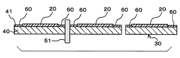
- FIG. 13 is a diagram illustrating a dicing process according to the seventh embodiment.
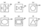
- FIG. 14A to FIG. 14F are diagrams showing examples of the planar pattern of the adhesive in the eighth embodiment.
- FIG. 15A and FIG. 15B are diagrams showing manufacturing steps according to the ninth embodiment.
- FIG. 16 is a diagram illustrating a manufacturing process according to the ninth embodiment.
- FIG. 17 is a plan view of a semiconductor chip according to the tenth embodiment
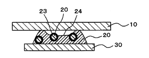
- FIG. 18 is a diagram showing an adhesive process according to the eleventh embodiment
- FIG. 19 is a diagram showing a mounting process according to the eleventh embodiment.
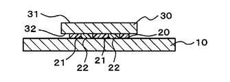
- FIG. 20 is a cross-sectional view of the semiconductor device completed by the mounting process shown in FIG. 21A is a plan view and a cross-sectional view of a semiconductor device without an adhesive leak path
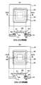
- FIG. 21B is a plan view and a cross-sectional view of a semiconductor device with an adhesive leak path.
- FIG. 22 is a diagram showing a mounting process according to the twelfth embodiment.
- FIG. 23 is a diagram illustrating a mounting process according to the thirteenth embodiment.
- the semiconductor device includes a substrate 10, an adhesive 20, and a semiconductor chip 30.
- the substrate 10 is formed with an electric circuit and serves as a base of the semiconductor device.
- a printed circuit board or a package is used as the substrate 10.
- the adhesive 20 is for fixing the semiconductor chip 30 to the substrate 10.
- a silicone-based adhesive is used as the adhesive 20. Silicone adhesives are softer than epoxy adhesives.
- the semiconductor chip 30 is a semiconductor chip having a predetermined structure formed on a semiconductor substrate.
- an inertial sensor structure such as an acceleration sensor or a yaw rate sensor is formed on the surface 31 side of the semiconductor chip 30.
- the back surface 32 side of the semiconductor chip 30 is fixed to the substrate 10 via the adhesive 20.
- the structure of the semiconductor chip 30 and the electric circuit of the substrate 10 are electrically connected by, for example, a bonding wire (not shown).
- a bonding wire not shown.
- a preparation process for preparing the semiconductor wafer 40 is performed.
- a fine structure such as an acceleration sensor is formed in units of semiconductor chips 30 by, for example, MEMS technology.
- an adhesive process is performed.
- the mask 50 is disposed on the one surface 41 of the semiconductor wafer 40.
- a metal mask or a mesh mask is used as the mask 50.
- the pattern of the mask 50 is a pattern in which a portion corresponding to each semiconductor chip 30 in the one surface 41 of the semiconductor wafer 40 is opened.
- the adhesive 20 is screen-printed on the one surface 41 of the semiconductor wafer 40 using the mask 50. As a result, the adhesive 20 is disposed at a predetermined position on the one surface 41 of the semiconductor wafer 40. Thus, since the adhesive 20 is arrange
- the adhesive 20 is not wasted. That is, since the adhesive 20 is disposed on the semiconductor wafer 40 as much as necessary, for example, a part of the size corresponding to the semiconductor chip 30 is not cut out from the roll-shaped adhesive sheet and the remaining adhesive sheet is not discarded. Therefore, there is a great effect in reducing the cost of the adhesive 20.
- the adhesive 20 may be directly screen-printed on the one surface 41 of the semiconductor wafer 40 without using the mask 50.
- a temporary curing process is performed.
- the adhesive 20 after the adhesive 20 is disposed on the one surface 41 of the semiconductor wafer 40 is temporarily cured.
- the adhesive 20 is temporarily cured by a method of heating the adhesive 20 or a method of irradiating the adhesive 20 with laser or ultraviolet rays. Thereby, the elastic modulus of the adhesive 20 that has been softened is improved.
- a dicing process is performed. That is, the semiconductor wafer 40 is fixed to a dicing tape (not shown), and the semiconductor wafer 40 is diced along the dotted line in FIG. Thus, the semiconductor wafer 40 is divided into individual semiconductor chips 30.
- the gap between the cutting line of the dicing blade 51 in the semiconductor wafer 40 and the adhesive 20 is between. There is a gap. Due to the presence of this gap, it is possible to prevent foreign matter that is shavings from adhering to the adhesive 20. Further, since the dicing blade 51 does not directly contact the adhesive 20, the adhesive 20 is not scraped or turned up by the dicing blade 51.
- the semiconductor wafer 40 is diced and cut in a state where the adhesive 20 is temporarily cured in the temporary curing step, it is possible to prevent the soft adhesive 20 from being caught in the dicing blade 51 as a foreign matter. Therefore, the dicing blade 51 can be diced and cut so that no foreign matter is caught in the dicing blade 51.
- a mounting process is performed in the process shown in FIG.
- the substrate 10 is prepared, and the semiconductor chip 30 is mounted on the substrate 10 via the adhesive 20.
- the semiconductor chip 30 is removed from the dicing tape and placed on the substrate 10.
- the adhesive 20 is fully cured by applying heat.
- the present embodiment is characterized in that the adhesive 20 is covered with a cover film.
- the adhesive 20 is disposed on one surface 41 of the semiconductor wafer 40, and after the temporary curing step shown in FIG. 2B, the semiconductor wafer 40 of the adhesive 20 is bonded to the semiconductor wafer 40 as shown in FIG. A cover film process of covering the non-contact portion with the cover film 52 is performed.
- the cover film 52 covers the pre-cured adhesive 20 and the cover film 52 covers a region of the one surface 41 of the semiconductor wafer 40 where the pre-cured adhesive 20 is not disposed.
- the semiconductor wafer 40 is fixed with a dicing tape 53.
- the cover film 52 and the semiconductor wafer 40 are diced with a dicing blade 51 from the cover film 52 side.
- the adhesive 20 is covered with the cover film 52, it is possible to prevent the coupling agent that determines the adhesiveness of the adhesive 20 from being washed from the adhesive 20 when the semiconductor wafer 40 is diced. . That is, a decrease in the coupling agent of the adhesive 20 can be prevented.
- the adhesive 20 is covered with the cover film 52, it is possible to prevent the shavings of the semiconductor wafer 40 from adhering to the adhesive 20.
- the adhesive 20 can be covered with the cover film 52.
- the cover film process is performed before the temporary curing process, the temporary curing process is performed after the cover film process, and the temporary curing process is performed. It is characterized by performing an adhesive process.
- a cover film 52 is prepared, and the adhesive 20 is screen-printed on the surface 55 of the cover film 52 on the one surface 41 side of the semiconductor wafer 40.
- the adhesive 20 is soft, in order to prevent the adhesive 20 from spreading, an adhesive having a recess 56 in which the surface 55 of the cover film 52 is recessed is used as shown in FIG. Therefore, the adhesive 20 is screen-printed on each recess 56 of the cover film 52.
- the surface 55 of the cover film 52 may include not only the surface that contacts the one surface 41 of the semiconductor wafer 40 but also the wall surface and bottom surface of the recessed portion 56.
- the temporary curing process is performed after this cover film process. Then, as shown in FIG. 8, the temporarily cured adhesive 20 is attached to one surface 41 of the semiconductor wafer 40 together with the cover film 52. As a result, the adhesive 20 is disposed on the one surface 41 of the semiconductor wafer 40, and the region of the one surface 41 of the semiconductor wafer 40 where the adhesive 20 is not disposed is covered with the cover film 52.
- the adhesive 20 may be disposed on the one surface 41 of the semiconductor wafer 40 after being applied to the cover film 52 and temporarily cured.
- the cover film process is performed before the adhesive 20 is disposed on the one surface 41 of the semiconductor wafer 40 and before the temporary curing process. That is, after the preparation step, the adhesive 20 is screen-printed on the cover film 52 as shown in FIG.
- the adhesive 20 is disposed on the one surface 41 of the semiconductor wafer 40, and the region of the one surface 41 of the semiconductor wafer 40 where the adhesive 20 is not disposed is covered with the cover film 52.
- the adhesive 20 is still soft. Therefore, the adhesive 20 is temporarily cured by performing the temporary curing step.
- the subsequent steps after the dicing step are the same as those in the second embodiment.
- the present embodiment is characterized in that a cover film 52 having a concavo-convex structure on the surface 55 is used.
- slit 57 shown in FIG. 9A and a protrusion 58 shown in FIG. 9B.
- These slits 57 and protrusions 58 are also provided on the bottom surface of the recessed portion 56. Note that the slit 57 and the protrusion 58 may be provided on the side surface of the recessed portion 56.
- the cover film 52 can be easily peeled off from the semiconductor wafer 40 by the uneven structure such as the slits 57 and the protrusions 58.
- the slit 57 and the protrusion 58 correspond to the “concavo-convex structure” of the scope of claims.
- the semiconductor chips 30 are removed one by one from the cover film 52 that is joined together and mounted on the substrate 10.
- the process can be simplified.
- the protective material process shown in FIG. 12 is performed after the adhesive process shown in FIG. 2A and the temporary curing process shown in FIG. 2B and before the dicing process.
- a protective material 60 that is harder than the adhesive 20 is disposed in a region of the one surface 41 of the semiconductor wafer 40 where the adhesive 20 is not disposed.
- a material made of polyimide is used as the protective material 60.
- the height of the protective material 60 with respect to the one surface 41 of the semiconductor wafer 40 is set lower than that of the adhesive 20. This prevents the protective material 60 from covering the adhesive 20.
- the semiconductor wafer 40 is diced and cut in a state where the protective material 60 is disposed on the one surface 41 of the semiconductor wafer 40.
- the protective material 60 is harder than the adhesive 20, it is difficult for foreign matter to be produced when the protective material 60 is shaved. For this reason, adhesion of a foreign substance to the adhesive 20 can be suppressed.
- the semiconductor chip 30 is mounted on the substrate 10. At this time, it may be mounted with the protective material 60 left on the semiconductor chip 30 removed, or may be mounted with the protective material 60 left on the semiconductor chip 30.
- the soft adhesive 20 can be continuously supported by the protective material 60. For this reason, deformation of the adhesive 20 can be suppressed when the semiconductor chip 30 is mounted.
- the present embodiment is characterized in that the adhesive 20 is arranged in a predetermined pattern in the adhesive process in the adhesive process.
- planar pattern of the adhesive 20 is a planar pattern of the adhesive 20 in one semiconductor chip 30. In other words, it is not a planar pattern on the entire surface 41 of one semiconductor wafer 40.
- the planar pattern of the adhesive 20 includes a cross shape in FIG. 14 (a), a bow tie shape in FIG. 14 (b), a round shape in FIG. 14 (c), that is, a circular shape, and FIG. An elliptical shape, a rectangular frame shape in FIG. 14E, or a triangular shape in FIG.
- the bow tie shape is a shape in which the apexes of two triangles overlap each other.
- the triangular shape is an example of a polygonal shape, and may be a quadrangular shape or a pentagonal shape.
- the planar pattern of the adhesive 20 is made to correspond to the structure formed on the semiconductor chip 30 when the semiconductor chip 30 is formed with a fine structure such as a comb-teeth structure of a capacitive acceleration sensor. Especially effective. That is, it is because the thermal distortion and mounting stress to the area
- the structure formed in the semiconductor chip 30 is not limited to the acceleration sensor, but may be another structure such as an angular velocity sensor.
- the present embodiment is characterized in that the structure of the semiconductor chip 30 and the electric circuit of the substrate 10 are electrically connected without connecting the structure of the semiconductor chip 30 and the electric circuit of the substrate 10 with bonding wires. Yes.
- the one surface 41 of the semiconductor wafer 40 is exposed as the adhesive 20 as shown in FIG. 15A.
- the one having the opening 21 to be disposed is disposed on one surface 41 of the semiconductor wafer 40. That is, the opening 21 is provided so that a pad (not shown) formed on the one surface 41 of the semiconductor wafer 40 is not covered with the adhesive 20.
- a conductive adhesive 22 is disposed in the opening 21.
- the conductive adhesive 22 is disposed on a pad (not shown) formed on the one surface 41 side of the semiconductor wafer 40 by a screen printing method or a dispensing method.
- This pad (not shown) is electrically connected to the structure on the other surface 42 side of the semiconductor wafer 40 by a through electrode or the like.
- a dicing process is performed, and in the subsequent mounting process, a substrate 10 having a pad formed at a position corresponding to the conductive adhesive 22 is prepared. Then, as shown in FIG. 16, the semiconductor chip 30 is mounted on the substrate 10, thereby electrically connecting the semiconductor chip 30 and the substrate 10 via the conductive adhesive 22.
- the semiconductor chip 30 can be connected to the semiconductor chip 30 via the conductive adhesive 22 without performing wire bonding.
- the substrate 10 can be electrically connected. For this reason, a wire bonding process can be omitted.
- the opening 21 provided in the adhesive 20 is not a through-hole, and the side surface of the adhesive 20 may be recessed inside, or one of the four corners of the adhesive 20 may be removed.
- the cover film 52 shown in the second to sixth embodiments may be used, or the protective material 60 shown in the seventh embodiment may be used.
- the adhesive 20 is not provided in the adhesive 20, but is applied to the end of the semiconductor chip 30 by, for example, a dispensing process. Further, a pad 33 is provided on the opposite side of the semiconductor chip 30 on the side where the adhesive 20 is disposed on the back surface 32 where the adhesive 20 is disposed.
- the adhesive 20 when the adhesive 20 is provided on a part of the back surface 32 of the semiconductor chip 30, the semiconductor chip 30 can be mounted on the substrate 10 in a cantilever manner. Thereby, since the area of the adhesive 20 to be used becomes smaller than each said embodiment, it becomes possible to further reduce stress.
- the present embodiment is characterized in that the timing of temporary curing of a part of the adhesive 20 is shifted. For this reason, in the adhesive process shown in FIG. 2A after the preparation process, as shown in FIG. 18, a part of the adhesive 20 sealed in the capsule 23 is used as a semiconductor wafer as shown in FIG. It is arranged at a predetermined position on one surface 41 of 40. In FIG. 18, one semiconductor chip 30 of the semiconductor wafer 40 is illustrated.
- the capsule 23 is a hollow spherical container and is a so-called shell.
- a material that does not contain a component that hardens the adhesive 20 is employed.
- acrylic resin is employed.
- the size of the capsule 23 is, for example, on the order of 100 ⁇ m. It is preferable that the capsule 23 has a waterproof property in consideration of the case where water is used in a later step of the adhesive process.
- a large number of capsules 23 are mixed in the adhesive 20 in advance. The number of capsules 23 mixed in the adhesive 20 is determined according to the viscosity of the adhesive 20, the temporarily cured shape of the adhesive 20 when the adhesive 20 is temporarily cured, and the like.
- the adhesive 20 in the capsule 23 and the adhesive 20 outside the capsule 23 are completely separated.
- the adhesive 20 in the capsule 23 is not affected by the outside of the capsule 23 unless the capsule 23 is broken.
- the outer edge of the adhesive 20 has a cornered shape as shown in FIG. That is, the groove 24 is formed in the central portion of the adhesive 20. This is because the adhesive 20 adhered to the opening of the mask 50 is lifted when the mask 50 is lifted from the semiconductor wafer 40 after the adhesive 20 is screen-printed on the one surface 41 of the semiconductor wafer 40 using the mask 50. This is because.
- a part of the adhesive 20 is temporarily cured in the temporary curing step shown in FIG.
- the adhesive 20 located outside the capsule 23 is temporarily cured without temporarily curing the adhesive 20 in the capsule 23. That is, the temporary curing timing of the adhesive 20 in the capsule 23 is changed with time. Specifically, by encapsulating a part of the adhesive 20 in the capsule 23, the timing for temporarily curing the adhesive 20 in the capsule 23 is set to be higher than the timing for temporarily curing the adhesive 20 outside the capsule 23. Delay.
- the adhesive 20 is fully cured by applying heat as shown in FIG.
- the acrylic resin constituting the capsule 23 is decomposed at 80 ° C., for example. That is, the capsule 23 is broken by heat applied to the adhesive 20 in order to fully cure the adhesive 20. That is, the curing timing of the adhesive 20 in the capsule 23 is not the timing of the temporary curing process but the timing of this mounting process.
- the semiconductor chip 30 is attached to the substrate 10 via the adhesive 20 that has not been temporarily cured in the temporary curing step, that is, the adhesive 20 enclosed in the capsule 23 and the adhesive 20 that has been temporarily cured in the temporary curing step.
- the fluid adhesive 20 enclosed in the capsule 23 that has not been temporarily cured flows out of the capsule 23 and is temporarily cured.
- the gap between the groove 24 of the agent 20 and the substrate 10 is filled. For this reason, it is possible to eliminate a leak path in which the groove 24 of the temporarily cured adhesive 20 is connected to the outside.
- the adhesion area and the sealing property of the adhesive 20 to the substrate 10 can be ensured.
- the thickness of the adhesive 20 is drawn to be thicker than the thickness of the substrate 10 or the semiconductor chip 30, so that the shape of the adhesive 20 can be understood schematically. It is. Therefore, actually, the adhesive 20 is sufficiently thinner than the substrate 10 and the semiconductor chip 30 as shown in FIG.
- the substrate 10 has a through hole 11 for introducing a pressure medium, as shown in FIGS. 21 (a) and 21 (b). is doing.
- the semiconductor chip 30 has a diaphragm 35 that is thinned by forming a recess 34 on the back surface 32.
- the semiconductor chip 30 When the pressure sensor for detecting the relative pressure as described above is formed in the semiconductor chip 30, it is necessary that the space on the front surface 31 side and the space on the back surface 32 side of the substrate 10 are completely separated. In other words, the semiconductor chip 30 needs to be bonded to the substrate 10 by the adhesive 20 provided on the back surface 32 of the substrate 10 so as to go around the diaphragm 35. When the entire adhesive 20 is temporarily cured at the same timing at a time, a leak path 25 occurs because a part of the adhesive 20 cannot secure a bonding area with the substrate 10 as shown in FIG. Resulting in. Thereby, there is a possibility that the relative pressure cannot be measured accurately.
- the circumference of the diaphragm 35 of the semiconductor chip 30 can be interrupted once around the substrate 10. It is possible to join with the adhesive 20 without any problem. That is, the leak path 25 can be eliminated, and the space on the front surface 31 side and the space on the back surface 32 side of the substrate 10 can be completely separated. Therefore, the relative pressure can be reliably detected in the pressure sensor.
- a substrate 10 whose mounting surface is not mirror-finished is prepared. That is, the mounting surface of the substrate 10 has an uneven shape 12.
- the uneven shape 12 of the substrate 10 may be positively formed. Further, the uneven shape 12 may be formed at least at a position on the substrate 10 where the semiconductor chip 30 is mounted.
- the substrate 10 is vibrated by applying a load of the substrate 10 to the temporarily cured adhesive 20.
- the capsule 23 is broken by the uneven shape 12 of the substrate 10.
- the capsule 23 located on the surface side of the temporarily cured adhesive 20 is mainly destroyed.
- the capsule 23 can be mechanically broken by the uneven shape 12 of the substrate 10.
- a resin that is easily broken mechanically may be selected as the material of the capsule 23.
- the substrate 10 but the semiconductor chip 30 may be vibrated.
- an organic solvent 13 such as acetone that can dissolve the acrylic resin on the mounting surface of the substrate 10.
- the organic solvent 13 capable of dissolving the resin may be applied to the mounting surface of the substrate 10.
- the capsule 23 can be chemically broken by melting the capsule 23.
- the semiconductor chip 30 may be moved to the substrate 10 side and the organic solvent 13 may be brought into contact with the capsule 23.
- the configurations of the semiconductor devices described in the above embodiments are examples, and the present invention is not limited to the configurations described above, and other configurations that can realize the present invention may be employed.
- the configuration of the semiconductor device described in each of the above embodiments is a minimum configuration, and the semiconductor device may be mounted on another substrate, a package, or the like.
- the semiconductor chips 30 that are diced and cut by providing the adhesive 20 on the semiconductor wafer 40 as described above may be stacked in order.
- the capsules 23 shown in the eleventh to thirteenth embodiments may be used for the adhesive 20 in the second to tenth embodiments.
- the method of destroying the capsule 23 is an example. Therefore, for example, the capsule 23 may be destroyed by heating with a laser or a liquid other than the organic solvent 13.
Landscapes
- Dicing (AREA)
- Die Bonding (AREA)
Abstract
半導体装置の製造方法は、半導体ウェハ(40)を用意し、前記半導体ウェハ(40)の所定の位置に接着剤(20)を配置し、前記半導体ウェハ(40)をダイシングカットして個々の半導体チップ(30)に分割し、基板(10)を用意し、前記基板(10)に前記接着剤(20)を介して前記半導体チップ(30)を実装し、前記接着剤(20)を仮硬化することを有する。前記接着剤の仮硬化は、前記接着剤の配置の前、または、前記接着剤の配置の後に行われる。前記接着剤の仮硬化は、前記ダイシングカットの前に行う。
Description
本開示は、2012年7月12日に出願された日本出願番号2012-156114号と、2013年2月5日に出願された日本出願番号2013-20067号に基づくもので、ここにその記載内容を援用する。
本開示は、半導体ウェハをダイシングカットして半導体チップに分割した後、半導体チップを基板に実装する半導体装置の製造方法に関するものである。
従来より、半導体ウェハのダイシング方法が、例えば特許文献1で提案されている。具体的に、特許文献1では、半導体ウェハの一面に接着剤を塗布し、接着剤側からダイシングブレードを入れて半導体ウェハのダイシングを行う方法が記載されている。
しかしながら、上記従来の技術では、接着剤として軟らかいものを用いた場合、半導体ウェハをダイシングカットするときに軟らかい接着剤を異物としてダイシングブレードに巻き込んでしまうという問題がある。
本開示は、導体ウェハに軟らかい接着剤を設けたとしても、異物を巻き込まないようにダイシングカットすることができる半導体装置の製造方法を提供することを目的とする。
本開示の第一の態様において、半導体装置の製造方法は、半導体ウェハを用意し、前記半導体ウェハの一面のうちの所定の位置に接着剤を配置し、前記半導体ウェハをダイシングカットすることにより、前記半導体ウェハを個々の半導体チップに分割し、基板を用意し、前記基板に前記接着剤を介して前記半導体チップを実装し、前記接着剤を仮硬化することを有している。前記接着剤の仮硬化は、前記接着剤の配置の前、または、前記接着剤の配置の後に行われる。前記接着剤の仮硬化は、前記ダイシングカットの前に行う。
上記の半導体装置の製造方法によると、仮硬化工程によって接着剤をある程度硬くしてから半導体ウェハをダイシングカットしているので、軟らかい接着剤を異物としてダイシングブレードに巻き込んでしまうことを防止することができる。したがって、半導体ウェハに軟らかい接着剤を設けたとしても、ダイシングブレードに異物を巻き込まないようにダイシングカットすることができる。
代案として、前記接着剤のうち前記半導体ウェハに接触しない部分をカバーフィルムで覆ってもよい。この場合、接着剤が半導体ウェハの一面に配置されたとき、接着剤がカバーフィルムによって覆われる。このため、接着性を決定づけるカップリング剤がダイシングカット時に接着剤から洗われてしまうことを防止することができる。すなわち、接着剤のカップリング剤の減少を防止することができる。
代案として、半導体装置の製造方法は、前記接着剤の配置及び前記接着剤の仮硬化の後、前記ダイシングカットの前に、前記半導体ウェハの一面のうち前記接着剤が配置されていない領域に、前記接着剤よりも硬い保護材を配置することをさらに含んでもよい。前記ダイシングカットでは、前記半導体ウェハの一面に前記保護材が配置された状態で前記半導体ウェハをダイシングカットする。この場合、半導体ウェハの一面のうち接着剤が配置されていない領域が保護材で覆われるので、当該領域に削りかすが付着したり、当該領域に付着した削りかすが接着剤に付着することを防止することができる。また、保護材は接着剤よりも硬いものであるため、保護材を削ったときに異物が出にくい。このため、接着剤への異物の付着を防止できる。
本開示についての上記目的およびその他の目的、特徴や利点は、添付の図面を参照しながら下記の詳細な記述により、より明確になる。その図面は、
図1は、第1実施形態に係る半導体装置の断面図であり、
図2(a)から図2(d)は、図1に示された半導体装置の製造工程を示した図であり、
図3は、第2実施形態に係る半導体装置の製造工程を示した図であり、
図4は、第2実施形態において、カバーフィルム側から半導体ウェハをダイシングカットする様子を示した図であり、
図5は、第2実施形態において、半導体チップからカバーフィルムをはがす様子を示した図であり、
図6は、第3実施形態において、カバーフィルムに接着剤を配置した様子を示した図であり、
図7は、第3実施形態に係るカバーフィルムの平面図であり、
図8は、第3実施形態に係る半導体装置の一製造工程を示した図であり、
図9(a)と図9(b)は、第5実施形態に係るカバーフィルムの表面の凹凸構造の一例を示した斜視図であり、
図10は、第6実施形態に係るダイシング工程を示した図であり、
図11は、第6実施形態において、カバーフィルムから半導体チップを取り外す様子を示した図であり、
図12は、第7実施形態に係る保護材工程を示した図であり、
図13は、第7実施形態に係るダイシング工程を示した図であり、
図14(a)から図14(f)は、第8実施形態において、接着剤の平面パターンの例を示した図であり、
図15(a)と図15(b)は、第9実施形態に係る製造工程を示した図であり、
図16は、第9実施形態に係る製造工程を示した図であり、
図17は、第10実施形態に係る半導体チップの平面図であり、
図18は、第11実施形態に係る接着剤工程を示した図であり、
図19は、第11実施形態に係る実装工程を示した図であり、
図20は、図19に示す実装工程により完成した半導体装置の断面図であり、
図21(a)は接着剤のリークパスが無い半導体装置の平面図及び断面図であり、図21(b)は接着剤のリークパスがある半導体装置の平面図及び断面図であり、
図22は、第12実施形態に係る実装工程を示した図であり、
図23は、第13実施形態に係る実装工程を示した図である。
以下、本発明の実施形態について図に基づいて説明する。なお、以下の各実施形態相互において、互いに同一もしくは均等である部分には、図中、同一符号を付してある。
(第1実施形態)
以下、本発明の第1実施形態について図を参照して説明する。図1に示されるように、本実施形態に係る半導体装置は、基板10と、接着剤20と、半導体チップ30と、を備えて構成されている。
以下、本発明の第1実施形態について図を参照して説明する。図1に示されるように、本実施形態に係る半導体装置は、基板10と、接着剤20と、半導体チップ30と、を備えて構成されている。
基板10は、電気回路が形成されたものであり、半導体装置の土台となるものである。基板10として、例えばプリント基板やパッケージが用いられる。
接着剤20は、半導体チップ30を基板10に固定するためのものである。接着剤20としてシリコーン系接着剤が用いられる。シリコーン系接着剤はエポキシ系接着剤よりも軟らかい接着剤である。
半導体チップ30は、半導体基板に所定の構造が形成された半導体チップである。半導体チップ30の表面31側には、例えば、加速度センサやヨーレートセンサ等の慣性センサの構造が形成されている。そして、半導体チップ30の裏面32側が接着剤20を介して基板10に固定されている。
なお、半導体チップ30の構造と基板10の電気回路は例えば図示しないボンディングワイヤによって電気的に接続されている。以上が、本実施形態に係る半導体装置の構成である。
次に、図1に示された半導体装置の製造方法について、図2(a)から図2(d)を参照して説明する。まず、半導体ウェハ40を用意する準備工程を行う。用意した半導体ウェハ40の一面41とは反対側の他面42側には、例えばMEMS技術により加速度センサ等の微細な構造が半導体チップ30単位で形成してある。
続いて、図2(a)に示す工程では、接着剤工程を行う。具体的には、半導体ウェハ40の一面41上にマスク50を配置する。マスク50として、例えばメタルマスクやメッシュマスク等を用いる。マスク50のパターンは、半導体ウェハ40の一面41のうち各半導体チップ30に対応した部分が開口したパターンである。
そして、マスク50を用いて接着剤20を半導体ウェハ40の一面41にスクリーン印刷する。これにより、半導体ウェハ40の一面41のうち所定の位置に接着剤20を配置する。このように半導体チップ30毎に接着剤20を配置するので、各半導体チップ30に対応した各接着剤20はそれぞれ接触することなく分離している。
このように、半導体ウェハ40の一面41のうち所定の位置に適量の接着剤20を配置しているので、接着剤20の無駄が出ない。すなわち、接着剤20を必要な分だけ半導体ウェハ40に配置するので、例えばロール状の接着シートから半導体チップ30に応じたサイズの一部を切り出して残りの接着シートを捨てるということはない。したがって、接着剤20のコストの削減に大きな効果がある。
なお、マスク50を用いずに半導体ウェハ40の一面41に接着剤20を直接スクリーン印刷しても良い。
続いて、図2(b)に示す工程では、仮硬化工程を行う。本実施形態では、半導体ウェハ40の一面41に接着剤20を配置した後の当該接着剤20を仮硬化する。具体的には、接着剤20を加熱する方法や、接着剤20にレーザや紫外線を照射する方法等により接着剤20を仮硬化する。これにより、軟らかかった接着剤20の弾性率を向上させる。
この後、図2(c)に示す工程では、ダイシング工程を行う。すなわち、半導体ウェハ40を図示しないダイシングテープに固定し、半導体ウェハ40の一面41に水を掛けながら、ダイシングブレード51で半導体ウェハ40を図2(c)の点線に沿ってダイシングカットする。これにより、半導体ウェハ40を個々の半導体チップ30に分割する。
ここで、上述のように、半導体ウェハ40の一面41全体ではなく所定の位置に接着剤20を配置しているので、半導体ウェハ40におけるダイシングブレード51のカットラインと接着剤20との間には隙間がある。この隙間の存在により、削りかすである異物が接着剤20に付着することを防止できる。また、ダイシングブレード51が接着剤20に直接接触しないので、ダイシングブレード51によって接着剤20が削れたりめくれたりすることもない。
そして、仮硬化工程において接着剤20を仮硬化させた状態で半導体ウェハ40をダイシングカットしているので、ダイシングブレード51に軟らかい接着剤20を異物として巻き込んでしまうことを防止することができる。したがって、ダイシングブレード51に異物を巻き込まないようにダイシングカットすることができる。
ダイシング工程の後、図2(d)に示す工程では、実装工程を行う。実装工程では、基板10を用意し、当該基板10に接着剤20を介して半導体チップ30を実装する。具体的には、ダイシングテープから半導体チップ30を取り外し、基板10の上に配置する。そして、熱を加えて接着剤20を本硬化する。
この後、ワイヤボンディング工程を行うことで半導体チップ30のセンサ構造と基板10の電気回路とを電気的に接続する。こうして、図1に示された半導体装置が完成する。
(第2実施形態)
本実施形態では、第1実施形態と異なる部分について説明する。本実施形態では、接着剤20をカバーフィルムで覆うことが特徴となっている。
本実施形態では、第1実施形態と異なる部分について説明する。本実施形態では、接着剤20をカバーフィルムで覆うことが特徴となっている。
具体的には、半導体ウェハ40の一面41に接着剤20を配置し、さらに上述の図2(b)に示す仮硬化工程の後、図3に示すように接着剤20のうち半導体ウェハ40に接触しない部分をカバーフィルム52で覆うカバーフィルム工程を行う。言い換えると、カバーフィルム52で仮硬化後の接着剤20を覆うと共に、半導体ウェハ40の一面41のうち仮硬化後の接着剤20が配置されていない領域をカバーフィルム52で覆う。なお、半導体ウェハ40をダイシングテープ53で固定してある。
この後、図2(c)に示すダイシング工程を行う。本実施形態では、図4に示すように、カバーフィルム52側からカバーフィルム52及び半導体ウェハ40をダイシングブレード51でダイシングカットする。ここで、接着剤20をカバーフィルム52で覆っているので、接着剤20の接着性を決定づけるカップリング剤が半導体ウェハ40のダイシングカット時に接着剤20から洗われてしまうことを防止することができる。つまり、接着剤20のカップリング剤の減少を防止できる。
また、接着剤20がカバーフィルム52に覆われるので、接着剤20に半導体ウェハ40の削りかすが付着することを防止することができる。
さらに、半導体ウェハ40の一面41のうち接着剤20が配置されていない領域がカバーフィルム52で覆われるので、当該領域に付着した削りかすが接着剤20に付着することを防止することができる。
こうして、半導体ウェハ40が各半導体チップ30に分割されると、各半導体チップ30にはカバーフィルム52の一部が乗った状態となっている。したがって、図2(d)に示す実装工程の前に、図5に示すように、ダイシング工程後のカバーフィルム52全体にテープ54を貼り、このテープ54を持ち上げることにより、各半導体チップ30からカバーフィルム52の断片をはがす。
この後、図2(d)に示す実装工程を行う。以上のように、カバーフィルム52で接着剤20を覆うこともできる。
(第3実施形態)
本実施形態では、上記各実施形態と異なる部分について説明する。本実施形態では、半導体ウェハ40の一面41に接着剤20を配置する前であって仮硬化工程の前にカバーフィルム工程を行い、カバーフィルム工程の後に仮硬化工程を行い、仮硬化工程の後に接着剤工程を行うことが特徴となっている。
本実施形態では、上記各実施形態と異なる部分について説明する。本実施形態では、半導体ウェハ40の一面41に接着剤20を配置する前であって仮硬化工程の前にカバーフィルム工程を行い、カバーフィルム工程の後に仮硬化工程を行い、仮硬化工程の後に接着剤工程を行うことが特徴となっている。
具体的には、準備工程の後、図6に示すように、カバーフィルム52を用意し、カバーフィルム52のうち半導体ウェハ40の一面41側の表面55に接着剤20をスクリーン印刷する。
接着剤20は軟らかいものであるので、接着剤20が広がらないようにするため、図7に示すように、カバーフィルム52の表面55が凹んだ凹み部56を有するものを用いる。したがって、カバーフィルム52の各凹み部56に接着剤20をスクリーン印刷する。なお、カバーフィルム52の表面55には、半導体ウェハ40の一面41に接触する面だけでなく、凹み部56の壁面及び底面を含めても良い。
このカバーフィルム工程の後に仮硬化工程を行う。そして、図8に示すように、仮硬化した接着剤20をカバーフィルム52と共に半導体ウェハ40の一面41に貼り付ける。これにより、接着剤20を半導体ウェハ40の一面41に配置すると共に、半導体ウェハ40の一面41のうち接着剤20が配置されていない領域をカバーフィルム52で覆う。
この後のダイシング工程以降の各工程は第2実施形態と同様である。以上のように、接着剤20をカバーフィルム52に塗布して仮硬化した後に半導体ウェハ40の一面41に配置しても良い。
(第4実施形態)
本実施形態では、第3実施形態と異なる部分について説明する。本実施形態では、半導体ウェハ40の一面41に接着剤20を配置する前であって仮硬化工程の前にカバーフィルム工程を行う。すなわち、準備工程の後、図6に示すように、カバーフィルム52に接着剤20をスクリーン印刷する。
本実施形態では、第3実施形態と異なる部分について説明する。本実施形態では、半導体ウェハ40の一面41に接着剤20を配置する前であって仮硬化工程の前にカバーフィルム工程を行う。すなわち、準備工程の後、図6に示すように、カバーフィルム52に接着剤20をスクリーン印刷する。
そして、このカバーフィルム工程の後に接着剤工程を行う。これにより、接着剤20を半導体ウェハ40の一面41に配置すると共に、半導体ウェハ40の一面41のうち接着剤20が配置されていない領域をカバーフィルム52で覆う。
この段階では、接着剤20はまだ軟らかい状態である。したがって、仮硬化工程を行うことにより、接着剤20を仮硬化する。この後のダイシング工程以降の各工程は第2実施形態と同様である。
(第5実施形態)
本実施形態では、第2~第4実施形態と異なる部分について説明する。本実施形態では、カバーフィルム52として表面55に凹凸構造が設けられたものを用いることが特徴となっている。
本実施形態では、第2~第4実施形態と異なる部分について説明する。本実施形態では、カバーフィルム52として表面55に凹凸構造が設けられたものを用いることが特徴となっている。
凹凸構造としては、例えば図9(a)に示すスリット57と、図9(b)に示す突起58がある。これらスリット57及び突起58は凹み部56の底面にも設けられている。なお、スリット57及び突起58は凹み部56の側面に設けられていても良い。
これらスリット57や突起58のような凹凸構造により、半導体ウェハ40からカバーフィルム52をはがしやすくすることができる。
なお、本実施形態の記載と特許請求の範囲の記載との対応関係については、スリット57及び突起58が特許請求の範囲の「凹凸構造」に対応する。
(第6実施形態)
本実施形態では、第2~第4実施形態と異なる部分について説明する。本実施形態では、図10に示すように、ダイシング工程において、半導体ウェハ40の一面41とは反対側の他面42側から半導体ウェハ40をダイシングブレード51でダイシングカットする。このとき、カバーフィルム52を完全に切断せずにハーフカットする。
本実施形態では、第2~第4実施形態と異なる部分について説明する。本実施形態では、図10に示すように、ダイシング工程において、半導体ウェハ40の一面41とは反対側の他面42側から半導体ウェハ40をダイシングブレード51でダイシングカットする。このとき、カバーフィルム52を完全に切断せずにハーフカットする。
そして、実装工程の際には、図11に示すように、ひとつなぎになったカバーフィルム52から半導体チップ30を一個ずつ取り外して基板10に実装する。このように、ダイシングカットされた各半導体チップ30からカバーフィルム52を取り外す必要がないので、工程の簡略化を図ることができる。
(第7実施形態)
本実施形態では、上記各実施形態と異なる部分について説明する。本実施形態では、図2(a)に示す接着剤工程及び図2(b)に示す仮硬化工程の後、ダイシング工程の前に、図12に示す保護材工程を行う。
本実施形態では、上記各実施形態と異なる部分について説明する。本実施形態では、図2(a)に示す接着剤工程及び図2(b)に示す仮硬化工程の後、ダイシング工程の前に、図12に示す保護材工程を行う。
具体的には、半導体ウェハ40の一面41のうち接着剤20が配置されていない領域に、接着剤20よりも硬い保護材60を配置する。保護材60として、例えばポリイミドで形成されたものを用いる。
半導体ウェハ40に保護材60を配置する際、半導体ウェハ40の一面41を基準とした保護材60の高さが接着剤20よりも低くなるようにする。これにより、保護材60が接着剤20を覆わないようにする。
この後、ダイシング工程では、図13に示すように、半導体ウェハ40の一面41に保護材60が配置された状態で半導体ウェハ40をダイシングカットする。これにより、半導体ウェハ40の一面41のうち接着剤20が配置されていない領域が保護材60で覆われているので、当該領域に削りかすが付着したり、当該領域に付着した削りかすが接着剤20に付着することを防止することができる。また、保護材60は接着剤20よりも硬いものであるため、保護材60を削ったときに異物が出にくい。このため、接着剤20への異物の付着を抑制できる。
実装工程では、半導体チップ30を基板10に実装する。このとき、半導体チップ30に残された保護材60を除去した状態で実装しても良いし、半導体チップ30に保護材60を残した状態で実装しても良い。
ダイシングカット後にも半導体チップ30に保護材60を残したまま半導体チップ30を基板10に実装する場合、保護材60によって軟らかい接着剤20を支え続けることができる。このため、半導体チップ30の実装時に接着剤20の変形を抑制することができる。
(第8実施形態)
本実施形態では、上記各実施形態と異なる部分について説明する。本実施形態では、接着剤工程において、接着剤20の平面パターンを所定のパターンに決めて接着剤20を配置することが特徴となっている。
本実施形態では、上記各実施形態と異なる部分について説明する。本実施形態では、接着剤工程において、接着剤20の平面パターンを所定のパターンに決めて接着剤20を配置することが特徴となっている。
ここで、接着剤20の平面パターンとは、1つの半導体チップ30における接着剤20の平面パターンである。言い換えると、1つの半導体ウェハ40の一面41全体における平面パターンではない。
具体的には、接着剤20の平面パターンとして、図14(a)の十字状、図14(b)の蝶ネクタイ状、図14(c)の丸状すなわち円形状、図14(d)の楕円状、図14(e)の四角枠状、図14(f)の三角形状とすることができる。
なお、蝶ネクタイ状とは、2個の三角形の一頂点部分が互いにオーバーラップした形状である。また、三角形状は多角形状の一例であり、四角形状や五角形状等でも良い。
半導体チップ30においては、接着剤20が塗布された領域に応力が掛かる。すなわち、図14(a)から図14(f)に示す各平面パターンにおいては、接着剤20が位置していない余白の部分に接着剤20の応力が掛からない。したがって、半導体チップ30に応力が掛かって欲しくない構造が形成されている場合、半導体チップ30の実装方向において当該構造と接着剤20とがオーバーラップしないような接着剤20の平面パターンを選択すれば良い。
このように接着剤20の平面パターンを半導体チップ30に形成された構造に対応させることは、半導体チップ30に静電容量式加速度センサの櫛歯構造等の微細な構造が形成されているものにおいて特に効果を発揮する。すなわち、半導体チップ30のうち接着剤20が塗布されていない領域への熱歪み及び実装応力を抑制できるからである。もちろん、半導体チップ30に形成されている構造は、加速度センサに限らず、角速度センサ等の他の構造でも良い。
また、半導体チップ30の実装応力を抑制できるので、半導体チップ30を基板10に組み付けた後の温度特性調整検査が不要になり、製造工程を簡略化できるという利点もある。
(第9実施形態)
本実施形態では、上記各実施形態と異なる部分について説明する。本実施形態では、ボンディングワイヤで半導体チップ30の構造と基板10の電気回路とを接続しなくても半導体チップ30の構造と基板10の電気回路とを電気的に接続することが特徴となっている。
本実施形態では、上記各実施形態と異なる部分について説明する。本実施形態では、ボンディングワイヤで半導体チップ30の構造と基板10の電気回路とを接続しなくても半導体チップ30の構造と基板10の電気回路とを電気的に接続することが特徴となっている。
具体的には、第1実施形態で説明した製造方法において、図2(a)に示す接着剤工程では、図15(a)に示すように接着剤20として、半導体ウェハ40の一面41を露出させる開口部21を有するものを半導体ウェハ40の一面41に配置する。すなわち、半導体ウェハ40の一面41に形成された図示しないパッドが接着剤20で覆われないように開口部21を設ける。
また、図15(b)に示すように、開口部21に導電性接着剤22を配置する。具体的には、半導体ウェハ40の一面41側に形成された図示しないパッドの上にスクリーン印刷の方法やディスペンス工程による方法により導電性接着剤22を配置する。この図示しないパッドは、半導体ウェハ40の他面42側の構造と貫通電極等で電気的に接続されている。
続いてダイシング工程を行い、この後の実装工程では、基板10には導電性接着剤22に対応した位置にパッドが形成されたものを用意する。そして、図16に示すように、半導体チップ30を基板10に実装することで導電性接着剤22を介して半導体チップ30と基板10とを電気的に接続する。
以上のように、接着剤20に予め開口部21を設けてこの開口部21に導電性接着剤22を配置することにより、ワイヤボンディングを行わずに導電性接着剤22を介して半導体チップ30と基板10とを電気的に接続することができる。このため、ワイヤボンディング工程を省略することができる。
接着剤20に設ける開口部21は貫通孔ではなく、接着剤20の側面が内側に凹んだり、接着剤20の四隅のいずれかの角が取れたりしたものでも良い。もちろん、本実施形態においても第2~第6実施形態で示したカバーフィルム52を用いても良いし、第7実施形態で示した保護材60を用いても良い。
(第10実施形態)
本実施形態では、第9実施形態と異なる部分について説明する。図17に示すように、接着剤20に開口部21を設けるのではなく、接着剤20を半導体チップ30の端に例えばディスペンス工程で塗布する。また、半導体チップ30のうち接着剤20を配置した裏面32において接着剤20が配置された側とは反対側にパッド33を設ける。
本実施形態では、第9実施形態と異なる部分について説明する。図17に示すように、接着剤20に開口部21を設けるのではなく、接着剤20を半導体チップ30の端に例えばディスペンス工程で塗布する。また、半導体チップ30のうち接着剤20を配置した裏面32において接着剤20が配置された側とは反対側にパッド33を設ける。
このように、半導体チップ30の裏面32の一部分に接着剤20を設けた場合は半導体チップ30を片持ちで基板10に実装することができる。これにより、用いる接着剤20の面積が上記各実施形態よりも小さくなるので、さらに低応力化が可能となる。
(第11実施形態)
本実施形態では、第1実施形態と異なる部分について説明する。本実施形態では、接着剤20のうちの一部の仮硬化のタイミングをずらすことが特徴となっている。このため、準備工程の後の図2(a)に示す接着剤工程では、図18に示すように、接着剤20として、当該接着剤20の一部をカプセル23に封入したものを、半導体ウェハ40の一面41のうち所定の位置に配置する。なお、図18では半導体ウェハ40のうちの1つの半導体チップ30を図示している。
本実施形態では、第1実施形態と異なる部分について説明する。本実施形態では、接着剤20のうちの一部の仮硬化のタイミングをずらすことが特徴となっている。このため、準備工程の後の図2(a)に示す接着剤工程では、図18に示すように、接着剤20として、当該接着剤20の一部をカプセル23に封入したものを、半導体ウェハ40の一面41のうち所定の位置に配置する。なお、図18では半導体ウェハ40のうちの1つの半導体チップ30を図示している。
カプセル23は中空球状の容器であり、いわゆる殻である。カプセル23の材料として、接着剤20を硬化させる成分が含まれていないものが採用される。例えばアクリル樹脂が採用される。また、カプセル23のサイズは、例えば100μmのオーダーである。カプセル23は接着剤工程の後工程で水が用いられる場合も考慮して防水性を有していることが好ましい。そして、多数のカプセル23を予め接着剤20に混入させている。接着剤20に混入させるカプセル23の数は、接着剤20の粘度や接着剤20を仮硬化したときの接着剤20の仮硬化形状等に応じて決まる。
このように、接着剤20は、その一部がカプセル23に封入されているので、カプセル23の中の接着剤20とカプセル23の外の接着剤20とは完全に分離されている。言い換えると、カプセル23の中の接着剤20はカプセル23が破壊されない限りカプセル23の外部の影響を受けない。
そして、接着剤20を半導体ウェハ40の一面41に配置すると、図18に示されるように、接着剤20の外縁部に角が立った形状になる。つまり、接着剤20の中央部に溝24が形成された状態となる。これは、マスク50を用いて接着剤20を半導体ウェハ40の一面41にスクリーン印刷した後、半導体ウェハ40からマスク50を持ち上げたときに、マスク50の開口部に付着した接着剤20が持ち上げられたためである。
なお、接着剤20の外縁部の角が立たないように接着剤20の粘度を下げることが考えられる。しかし、接着剤20の外縁部が形状を保持できずに垂れてしまう。その結果、接着剤20は中央部が突出した円錐のような形状となるため、接着剤20と基板10との接着面積を確保できない。したがって、接着剤20の粘度を下げることは好ましくない。
続いて、図2(b)に示す仮硬化工程において接着剤20のうちの一部分を仮硬化する。これにより、カプセル23の中の接着剤20を仮硬化させずにカプセル23の外に位置する接着剤20を仮硬化する。すなわち、カプセル23の中の接着剤20についての仮硬化のタイミングを時間的に変化させる。具体的には、接着剤20の一部をカプセル23に封入することにより、カプセル23の中の接着剤20を仮硬化するタイミングを、カプセル23の外の接着剤20を仮硬化するタイミングよりも遅らせる。
そして、図2(c)に示すダイシング工程を行った後の図2(d)に示す実装工程では、図19に示すように、熱を加えて接着剤20を本硬化する。このとき、カプセル23を構成するアクリル樹脂は例えば80℃で分解する。すなわち、接着剤20を本硬化するために接着剤20に与える熱によってカプセル23を破壊する。つまり、カプセル23の中の接着剤20の硬化タイミングは仮硬化工程のタイミングではなくこの実装工程のタイミングとなる。このようにして、仮硬化工程で仮硬化していない接着剤20すなわちカプセル23に封入した接着剤20、及び、仮硬化工程で仮硬化した接着剤20を介して、基板10に半導体チップ30を実装する。
そして、上記のようにカプセル23を破壊することにより、図20に示すように、仮硬化していないカプセル23に封入されていた流動性のある接着剤20がカプセル23から流れ出て仮硬化した接着剤20の溝24と基板10との間の隙間を埋める。このため、仮硬化した接着剤20の溝24と外部とが繋がってしまうリークパスを無くすことができる。また、基板10に対する接着剤20の接着面積及びシール性を確保することができる。
なお、上述の図18~図20では、接着剤20の厚みが基板10や半導体チップ30の厚みよりも厚く描かれているが、これは接着剤20の形状を模式的に理解できるようにしたためである。したがって、実際には図1のように接着剤20は基板10や半導体チップ30よりも十分薄い。
このようなリークパス解消の効果は、半導体チップ30として圧力センサを採用した場合には特に有効である。例えば、圧力センサが相対圧を検出するように構成されている場合、図21(a)及び図21(b)に示されるように、基板10は圧力媒体を導入するための貫通孔11を有している。また、半導体チップ30は、裏面32に凹部34が形成されたことにより薄膜化されたダイヤフラム35を有している。ダイヤフラム35が半導体チップ30の表面31側から受ける圧力と基板10の貫通孔11を介して裏面32側から受ける圧力との圧力差によってたわみ、このたわみ量に応じて相対圧が検出される構成となっている。
上記のような相対圧を検出する圧力センサが半導体チップ30に形成されている場合、基板10の表面31側の空間と裏面32側の空間とが完全に分離されていることが必要である。言い換えると、半導体チップ30が、ダイヤフラム35の周囲を一周するように基板10の裏面32に設けられた接着剤20によって基板10に接合されていることが必要である。そして、接着剤20の全体を同じタイミングで一度に仮硬化した場合、図21(b)に示されるように接着剤20の一部で基板10との接着面積を確保できずにリークパス25が発生してしまう。これにより、相対圧を正確に測定できない可能性がある。
しかしながら、本発明のように接着剤20の一部の仮硬化のタイミングを遅らせることにより、図21(a)に示されるように、基板10に対して半導体チップ30のダイヤフラム35の周囲を一周途切れることなく接着剤20で接合することができる。すなわち、リークパス25を解消することができ、基板10の表面31側の空間と裏面32側の空間と完全に分離することができる。したがって、圧力センサにおいて相対圧を確実に検出できるようにすることができる。
(第12実施形態)
本実施形態では、第11実施形態と異なる部分について説明する。本実施形態では、実装工程において、接着剤20に混入させたカプセル23を機械的に破壊することが特徴となっている。
本実施形態では、第11実施形態と異なる部分について説明する。本実施形態では、実装工程において、接着剤20に混入させたカプセル23を機械的に破壊することが特徴となっている。
具体的には、図22に示すように、基板10のうちの実装面が鏡面加工されていないものを用意する。すなわち、基板10の実装面は凹凸形状12になっている。なお、カプセル23を破壊しやすくするために、基板10の凹凸形状12を積極的に形成しても良い。また、凹凸形状12は基板10のうち少なくとも半導体チップ30が実装される位置に形成されていれば良い。
そして、図22に示すように、仮硬化した接着剤20に基板10の荷重をかけて基板10を振動させる。これにより、基板10の凹凸形状12によってカプセル23を破壊する。この場合、仮硬化した接着剤20の表面側に位置するカプセル23を主に破壊することとなる。
以上のように、基板10の凹凸形状12によって機械的にカプセル23を破壊することもできる。なお、カプセル23の材料として機械的に破壊しやすい樹脂を選択しても良い。また、基板10ではなく半導体チップ30を振動させても良い。
(第13実施形態)
本実施形態では、第11、第12実施形態と異なる部分について説明する。本実施形態では、実装工程において、接着剤20に混入させたカプセル23を化学的に破壊することが特徴となっている。
本実施形態では、第11、第12実施形態と異なる部分について説明する。本実施形態では、実装工程において、接着剤20に混入させたカプセル23を化学的に破壊することが特徴となっている。
具体的には、上述のようにカプセル23の殻としてアクリル樹脂を用いているので、図23に示すように、基板10のうちの実装面にアクリル樹脂を溶かすことができるアセトン等の有機溶媒13を塗布したものを用意する。もちろん、カプセル23の殻として他の樹脂を採用した場合には当該樹脂を溶かすことができる有機溶媒13を基板10の実装面に塗布すれば良い。
そして、図23に示すように、基板10を仮硬化した接着剤20に押しつけることにより、有機溶媒13によってカプセル23を溶かして破壊する。この場合、仮硬化した接着剤20の表面に位置するカプセル23を破壊することとなる。
以上のように、カプセル23を溶かすことによって化学的にカプセル23を破壊することもできる。なお、半導体チップ30を基板10側に移動させて有機溶媒13をカプセル23に接触させても良い。
(他の実施形態)
上記各実施形態で示された半導体装置の構成は一例であり、上記で示した構成に限定されることなく、本発明を実現できる他の構成とすることもできる。例えば、上記各実施形態で示した半導体装置の構成は最小構成であり、当該半導体装置を他の基板やパッケージ等に実装しても構わない。また、半導体チップ30を複数積層する場合にも、上記のように半導体ウェハ40に接着剤20を設けてダイシングカットした半導体チップ30を順に積層していけば良い。
上記各実施形態で示された半導体装置の構成は一例であり、上記で示した構成に限定されることなく、本発明を実現できる他の構成とすることもできる。例えば、上記各実施形態で示した半導体装置の構成は最小構成であり、当該半導体装置を他の基板やパッケージ等に実装しても構わない。また、半導体チップ30を複数積層する場合にも、上記のように半導体ウェハ40に接着剤20を設けてダイシングカットした半導体チップ30を順に積層していけば良い。
第11~第13実施形態で示されたカプセル23については、第2~第10実施形態の接着剤20に採用しても良い。また、上述のカプセル23を破壊する方法は一例である。したがって、例えばレーザによる加熱や有機溶媒13以外の他の液体等によってカプセル23を破壊しても良い。
本開示は、実施例に準拠して記述されたが、本開示は当該実施例や構造に限定されるものではないと理解される。本開示は、様々な変形例や均等範囲内の変形をも包含する。加えて、様々な組み合わせや形態、さらには、それらに一要素のみ、それ以上、あるいはそれ以下、を含む他の組み合わせや形態をも、本開示の範疇や思想範囲に入るものである。
Claims (16)
- 半導体ウェハ(40)を用意し、
前記半導体ウェハ(40)の一面(41)のうちの所定の位置に接着剤(20)を配置し、
前記半導体ウェハ(40)をダイシングカットすることにより、前記半導体ウェハ(40)を個々の半導体チップ(30)に分割し、
基板(10)を用意し、前記基板(10)に前記接着剤(20)を介して前記半導体チップ(30)を実装し、
前記接着剤(20)を仮硬化することを有しており、
前記接着剤の仮硬化は、前記接着剤の配置の前、または、前記接着剤の配置の後に行われ、
前記接着剤の仮硬化は、前記ダイシングカットの前に行う半導体装置の製造方法。 - 前記接着剤(20)のうち前記半導体ウェハ(40)に接触しない部分をカバーフィルム(52)で覆うことを、さらに含んでいる請求項1に記載の半導体装置の製造方法。
- 前記カバーフィルムで覆うことは、前記接着剤の配置の後であって前記接着剤の仮硬化の後、かつ、前記ダイシングカットの前に行い、
前記カバーフィルム(52)で前記接着剤(20)を覆うと共に、前記半導体ウェハ(40)の一面(41)のうち前記接着剤(20)が配置されていない領域を前記カバーフィルム(52)で覆う請求項2に記載の半導体装置の製造方法。 - 前記接着剤の配置前であって、前記接着剤の仮硬化の前に、前記カバーフィルムで覆うことを行い、
前記カバーフィルムで覆うことの後に、前記接着剤の仮硬化を行い、
前記接着剤の仮硬化の後に、前記接着剤の配置を行い
前記半導体ウェハ(40)の一面(41)のうち前記接着剤(20)が配置されていない領域を、前記カバーフィルム(52)で覆う請求項2に記載の半導体装置の製造方法。 - 前記接着剤の配置の前であって、前記接着剤の仮硬化の前に、前記カバーフィルムで覆うことを行い、
前記カバーフィルムで覆うことの後に、前記接着剤の配置を行い、
前記半導体ウェハ(40)の一面(41)のうち前記接着剤(20)が配置されていない領域を前記カバーフィルム(52)で覆い、
前記接着剤の配置の後、前記仮硬化工程を行う請求項2に記載の半導体装置の製造方法。 - 前記カバーフィルムで覆うことにおいて、前記カバーフィルム(52)は、前記半導体ウェハ(40)の一面(41)側の表面(55)に、凹凸構造(57、58)を有する請求項2ないし5のいずれか1つに記載の半導体装置の製造方法。
- 前記ダイシングカットでは、前記半導体ウェハ(40)の一面(41)とは反対側の他面(42)側から前記半導体ウェハ(40)をダイシングカットすると共に、前記カバーフィルム(52)をハーフカットする請求項2ないし6のいずれか1つに記載の半導体装置の製造方法。
- 前記ダイシングカットでは、前記カバーフィルム(52)側から前記カバーフィルム(52)及び前記半導体ウェハ(40)をダイシングカットする請求項2ないし6のいずれか1つに記載の半導体装置の製造方法。
- 前記接着剤の配置及び前記接着剤の仮硬化の後、前記ダイシングカットの前に、前記半導体ウェハ(40)の一面(41)のうち前記接着剤(20)が配置されていない領域に、前記接着剤(20)よりも硬い保護材(60)を配置することをさらに含み、
前記ダイシングカットでは、前記半導体ウェハ(40)の一面(41)に前記保護材(60)が配置された状態で前記半導体ウェハ(40)をダイシングカットする請求項1に記載の半導体装置の製造方法。 - 前記半導体チップ(30)の実装は、前記半導体チップ(30)に前記保護材(60)を残したまま、前記半導体チップ(30)を前記基板(10)に実装する請求項9に記載の半導体装置の製造方法。
- 前記接着剤の配置では、前記接着剤(20)をスクリーン印刷する請求項1ないし10のいずれか1つに記載の半導体装置の製造方法。
- 前記接着剤の仮硬化では、前記接着剤(20)のうちの一部分を仮硬化し、
前記半導体チップの実装では、前記接着剤(20)のうち前記接着剤の仮硬化で仮硬化した部分及び仮硬化していない部分を介して、前記基板(10)に前記半導体チップ(30)を実装する請求項1ないし11のいずれか1つに記載の半導体装置の製造方法。 - 前記接着剤の配置では、当該接着剤(20)の一部はカプセル(23)に封入されており、
前記接着剤の仮硬化では、前記カプセル(23)の外に位置する接着剤の他の部分を仮硬化し、
前記半導体チップの実装では、前記カプセル(23)を破壊すると共に、前記カプセル(23)に封入した接着剤(20)及び前記接着剤の仮硬化で仮硬化した接着剤(20)を介して、前記基板(10)に前記半導体チップ(30)を実装する請求項12に記載の半導体装置の製造方法。 - 前記接着剤の配置では、前記接着剤(20)の平面パターンが丸、十字、多角形のいずれか一つとなるように、前記接着剤(20)を配置する請求項1ないし13のいずれか1つに半導体装置の製造方法。
- 前記接着剤(20)は、前記半導体ウェハ(40)の一面(41)を露出させる開口部(21)を有し、
前記接着剤の配置では、接着剤を前記半導体ウェハ(40)の一面(41)に配置すると共に、前記開口部(21)に導電性接着剤(22)を配置し、
前記半導体チップの実装では、前記導電性接着剤(22)を介して前記半導体チップ(30)と前記基板(10)とを電気的に接続する請求項1ないし14のいずれか1つに記載の半導体装置の製造方法。 - 前記接着剤の配置では、前記接着剤(20)はシリコーン系接着剤である請求項1ないし15のいずれか1つに記載の半導体装置の製造方法。
Applications Claiming Priority (4)
| Application Number | Priority Date | Filing Date | Title |
|---|---|---|---|
| JP2012156114 | 2012-07-12 | ||
| JP2012-156114 | 2012-07-12 | ||
| JP2013020067A JP2014033177A (ja) | 2012-07-12 | 2013-02-05 | 半導体装置の製造方法 |
| JP2013-020067 | 2013-02-05 |
Publications (1)
| Publication Number | Publication Date |
|---|---|
| WO2014010237A1 true WO2014010237A1 (ja) | 2014-01-16 |
Family
ID=49915718
Family Applications (1)
| Application Number | Title | Priority Date | Filing Date |
|---|---|---|---|
| PCT/JP2013/004255 Ceased WO2014010237A1 (ja) | 2012-07-12 | 2013-07-10 | 半導体装置の製造方法 |
Country Status (2)
| Country | Link |
|---|---|
| JP (1) | JP2014033177A (ja) |
| WO (1) | WO2014010237A1 (ja) |
Cited By (1)
| Publication number | Priority date | Publication date | Assignee | Title |
|---|---|---|---|---|
| CN114093814A (zh) * | 2021-11-12 | 2022-02-25 | 无锡微视传感科技有限公司 | 一种双面结构的圆片的划片方法 |
Families Citing this family (3)
| Publication number | Priority date | Publication date | Assignee | Title |
|---|---|---|---|---|
| JP6292432B2 (ja) * | 2013-01-15 | 2018-03-14 | ナガセケムテックス株式会社 | 回路部材接合体の製造方法および回路部材 |
| WO2019058429A1 (ja) * | 2017-09-19 | 2019-03-28 | 日立化成株式会社 | 半導体装置製造用接着フィルム及びその製造方法 |
| WO2019058425A1 (ja) * | 2017-09-19 | 2019-03-28 | 日立化成株式会社 | 半導体装置製造用接着フィルム |
Citations (10)
| Publication number | Priority date | Publication date | Assignee | Title |
|---|---|---|---|---|
| JPS61180442A (ja) * | 1985-02-05 | 1986-08-13 | Toshiba Corp | 半導体装置の製造方法 |
| JP2001156027A (ja) * | 1999-11-30 | 2001-06-08 | Lintec Corp | 半導体装置の製造方法 |
| JP2002319647A (ja) * | 2001-04-24 | 2002-10-31 | Oki Electric Ind Co Ltd | 半導体装置の製造方法 |
| JP2004006954A (ja) * | 1997-03-24 | 2004-01-08 | Seiko Epson Corp | 半導体装置 |
| JP2007165841A (ja) * | 2005-11-16 | 2007-06-28 | Denso Corp | 半導体基板およびシートの接着方法 |
| JP2011023692A (ja) * | 2009-06-15 | 2011-02-03 | Sekisui Chem Co Ltd | ダイシング−ダイボンディングテープ及びその製造方法、並びに半導体チップの製造方法 |
| JP2011109022A (ja) * | 2009-11-20 | 2011-06-02 | Hitachi Chem Co Ltd | 半導体チップの製造方法及び加工用フィルム |
| JP2011222593A (ja) * | 2010-04-05 | 2011-11-04 | Hitachi Chem Co Ltd | 半導体装置の製造方法 |
| JP2011253940A (ja) * | 2010-06-02 | 2011-12-15 | Sony Chemical & Information Device Corp | ウエハのダイシング方法、接続方法及び接続構造体 |
| JP2012084759A (ja) * | 2010-10-14 | 2012-04-26 | Denki Kagaku Kogyo Kk | 電子部品の製造方法 |
-
2013
- 2013-02-05 JP JP2013020067A patent/JP2014033177A/ja active Pending
- 2013-07-10 WO PCT/JP2013/004255 patent/WO2014010237A1/ja not_active Ceased
Patent Citations (10)
| Publication number | Priority date | Publication date | Assignee | Title |
|---|---|---|---|---|
| JPS61180442A (ja) * | 1985-02-05 | 1986-08-13 | Toshiba Corp | 半導体装置の製造方法 |
| JP2004006954A (ja) * | 1997-03-24 | 2004-01-08 | Seiko Epson Corp | 半導体装置 |
| JP2001156027A (ja) * | 1999-11-30 | 2001-06-08 | Lintec Corp | 半導体装置の製造方法 |
| JP2002319647A (ja) * | 2001-04-24 | 2002-10-31 | Oki Electric Ind Co Ltd | 半導体装置の製造方法 |
| JP2007165841A (ja) * | 2005-11-16 | 2007-06-28 | Denso Corp | 半導体基板およびシートの接着方法 |
| JP2011023692A (ja) * | 2009-06-15 | 2011-02-03 | Sekisui Chem Co Ltd | ダイシング−ダイボンディングテープ及びその製造方法、並びに半導体チップの製造方法 |
| JP2011109022A (ja) * | 2009-11-20 | 2011-06-02 | Hitachi Chem Co Ltd | 半導体チップの製造方法及び加工用フィルム |
| JP2011222593A (ja) * | 2010-04-05 | 2011-11-04 | Hitachi Chem Co Ltd | 半導体装置の製造方法 |
| JP2011253940A (ja) * | 2010-06-02 | 2011-12-15 | Sony Chemical & Information Device Corp | ウエハのダイシング方法、接続方法及び接続構造体 |
| JP2012084759A (ja) * | 2010-10-14 | 2012-04-26 | Denki Kagaku Kogyo Kk | 電子部品の製造方法 |
Cited By (1)
| Publication number | Priority date | Publication date | Assignee | Title |
|---|---|---|---|---|
| CN114093814A (zh) * | 2021-11-12 | 2022-02-25 | 无锡微视传感科技有限公司 | 一种双面结构的圆片的划片方法 |
Also Published As
| Publication number | Publication date |
|---|---|
| JP2014033177A (ja) | 2014-02-20 |
Similar Documents
| Publication | Publication Date | Title |
|---|---|---|
| US8962389B2 (en) | Microelectronic packages including patterned die attach material and methods for the fabrication thereof | |
| JP6271151B2 (ja) | キャビティ型半導体パッケージおよびそのパッケージング方法 | |
| KR20070064322A (ko) | 기능 소자 실장 모듈 및 그 제조 방법 | |
| JP2009054979A (ja) | 電子装置および電子装置の製造方法 | |
| WO2014010237A1 (ja) | 半導体装置の製造方法 | |
| JP6059074B2 (ja) | 半導体装置の製造方法 | |
| CN101499456A (zh) | 半导体器件及其制造方法 | |
| US11390519B2 (en) | Method for manufacturing a MEMS sensor | |
| JP4366666B1 (ja) | 半導体装置 | |
| US8748926B2 (en) | Chip package with multiple spacers and method for forming the same | |
| JP4678240B2 (ja) | 半導体素子の製造方法 | |
| JP2005286284A (ja) | 機能素子実装モジュール並びに光機能素子実装モジュール及びその製造方法 | |
| JP5775707B2 (ja) | 半導体装置および半導体装置の製造方法 | |
| CN111261647A (zh) | 一种透光盖板、光学传感器及其制造方法 | |
| CN207637778U (zh) | 一种芯片的封装结构 | |
| CN108091616B (zh) | 一种芯片的封装方法以及封装结构 | |
| JP2001250843A (ja) | 半導体素子及び半導体素子製造方法 | |
| CN102344109A (zh) | 封装结构及其制造方法 | |
| JP2009295900A (ja) | 封止構造の製造方法 | |
| JP4862986B2 (ja) | 半導体装置の製造方法 | |
| TWI549268B (zh) | 晶圓封裝方法 | |
| TW201208006A (en) | Package structure and manufacturing method thereof | |
| JP5384693B2 (ja) | 半導体パッケージ | |
| JP2008182026A (ja) | 機能素子実装モジュールの製造方法 | |
| WO2012168959A1 (ja) | 半導体チップ、これを備えた半導体装置および半導体チップの製造方法 |
Legal Events
| Date | Code | Title | Description |
|---|---|---|---|
| 121 | Ep: the epo has been informed by wipo that ep was designated in this application |
Ref document number: 13817042 Country of ref document: EP Kind code of ref document: A1 |
|
| NENP | Non-entry into the national phase |
Ref country code: DE |
|
| 122 | Ep: pct application non-entry in european phase |
Ref document number: 13817042 Country of ref document: EP Kind code of ref document: A1 |