WO2014007250A1 - 酸化亜鉛薄膜の製造方法、薄膜トランジスタの製造方法、酸化亜鉛薄膜、薄膜トランジスタおよび透明酸化物配線 - Google Patents
酸化亜鉛薄膜の製造方法、薄膜トランジスタの製造方法、酸化亜鉛薄膜、薄膜トランジスタおよび透明酸化物配線 Download PDFInfo
- Publication number
- WO2014007250A1 WO2014007250A1 PCT/JP2013/068136 JP2013068136W WO2014007250A1 WO 2014007250 A1 WO2014007250 A1 WO 2014007250A1 JP 2013068136 W JP2013068136 W JP 2013068136W WO 2014007250 A1 WO2014007250 A1 WO 2014007250A1
- Authority
- WO
- WIPO (PCT)
- Prior art keywords
- thin film
- zinc oxide
- oxide thin
- zinc
- producing
- Prior art date
- Legal status (The legal status is an assumption and is not a legal conclusion. Google has not performed a legal analysis and makes no representation as to the accuracy of the status listed.)
- Ceased
Links
Images


Classifications
-
- H—ELECTRICITY
- H10—SEMICONDUCTOR DEVICES; ELECTRIC SOLID-STATE DEVICES NOT OTHERWISE PROVIDED FOR
- H10D—INORGANIC ELECTRIC SEMICONDUCTOR DEVICES
- H10D99/00—Subject matter not provided for in other groups of this subclass
-
- C—CHEMISTRY; METALLURGY
- C25—ELECTROLYTIC OR ELECTROPHORETIC PROCESSES; APPARATUS THEREFOR
- C25D—PROCESSES FOR THE ELECTROLYTIC OR ELECTROPHORETIC PRODUCTION OF COATINGS; ELECTROFORMING; APPARATUS THEREFOR
- C25D17/00—Constructional parts, or assemblies thereof, of cells for electrolytic coating
- C25D17/001—Apparatus specially adapted for electrolytic coating of wafers, e.g. semiconductors or solar cells
-
- C—CHEMISTRY; METALLURGY
- C25—ELECTROLYTIC OR ELECTROPHORETIC PROCESSES; APPARATUS THEREFOR
- C25D—PROCESSES FOR THE ELECTROLYTIC OR ELECTROPHORETIC PRODUCTION OF COATINGS; ELECTROFORMING; APPARATUS THEREFOR
- C25D5/00—Electroplating characterised by the process; Pretreatment or after-treatment of workpieces
- C25D5/02—Electroplating of selected surface areas
-
- C—CHEMISTRY; METALLURGY
- C25—ELECTROLYTIC OR ELECTROPHORETIC PROCESSES; APPARATUS THEREFOR
- C25D—PROCESSES FOR THE ELECTROLYTIC OR ELECTROPHORETIC PRODUCTION OF COATINGS; ELECTROFORMING; APPARATUS THEREFOR
- C25D9/00—Electrolytic coating other than with metals
- C25D9/04—Electrolytic coating other than with metals with inorganic materials
- C25D9/08—Electrolytic coating other than with metals with inorganic materials by cathodic processes
-
- H—ELECTRICITY
- H10—SEMICONDUCTOR DEVICES; ELECTRIC SOLID-STATE DEVICES NOT OTHERWISE PROVIDED FOR
- H10D—INORGANIC ELECTRIC SEMICONDUCTOR DEVICES
- H10D30/00—Field-effect transistors [FET]
- H10D30/60—Insulated-gate field-effect transistors [IGFET]
- H10D30/67—Thin-film transistors [TFT]
- H10D30/674—Thin-film transistors [TFT] characterised by the active materials
- H10D30/6755—Oxide semiconductors, e.g. zinc oxide, copper aluminium oxide or cadmium stannate
-
- H—ELECTRICITY
- H10—SEMICONDUCTOR DEVICES; ELECTRIC SOLID-STATE DEVICES NOT OTHERWISE PROVIDED FOR
- H10D—INORGANIC ELECTRIC SEMICONDUCTOR DEVICES
- H10D62/00—Semiconductor bodies, or regions thereof, of devices having potential barriers
- H10D62/80—Semiconductor bodies, or regions thereof, of devices having potential barriers characterised by the materials
-
- H—ELECTRICITY
- H10—SEMICONDUCTOR DEVICES; ELECTRIC SOLID-STATE DEVICES NOT OTHERWISE PROVIDED FOR
- H10D—INORGANIC ELECTRIC SEMICONDUCTOR DEVICES
- H10D64/00—Electrodes of devices having potential barriers
- H10D64/60—Electrodes characterised by their materials
- H10D64/62—Electrodes ohmically coupled to a semiconductor
-
- H—ELECTRICITY
- H10—SEMICONDUCTOR DEVICES; ELECTRIC SOLID-STATE DEVICES NOT OTHERWISE PROVIDED FOR
- H10D—INORGANIC ELECTRIC SEMICONDUCTOR DEVICES
- H10D86/00—Integrated devices formed in or on insulating or conducting substrates, e.g. formed in silicon-on-insulator [SOI] substrates or on stainless steel or glass substrates
- H10D86/01—Manufacture or treatment
- H10D86/021—Manufacture or treatment of multiple TFTs
- H10D86/0241—Manufacture or treatment of multiple TFTs using liquid deposition, e.g. printing
-
- H—ELECTRICITY
- H10—SEMICONDUCTOR DEVICES; ELECTRIC SOLID-STATE DEVICES NOT OTHERWISE PROVIDED FOR
- H10D—INORGANIC ELECTRIC SEMICONDUCTOR DEVICES
- H10D86/00—Integrated devices formed in or on insulating or conducting substrates, e.g. formed in silicon-on-insulator [SOI] substrates or on stainless steel or glass substrates
- H10D86/40—Integrated devices formed in or on insulating or conducting substrates, e.g. formed in silicon-on-insulator [SOI] substrates or on stainless steel or glass substrates characterised by multiple TFTs
- H10D86/441—Interconnections, e.g. scanning lines
-
- H—ELECTRICITY
- H10—SEMICONDUCTOR DEVICES; ELECTRIC SOLID-STATE DEVICES NOT OTHERWISE PROVIDED FOR
- H10D—INORGANIC ELECTRIC SEMICONDUCTOR DEVICES
- H10D86/00—Integrated devices formed in or on insulating or conducting substrates, e.g. formed in silicon-on-insulator [SOI] substrates or on stainless steel or glass substrates
- H10D86/40—Integrated devices formed in or on insulating or conducting substrates, e.g. formed in silicon-on-insulator [SOI] substrates or on stainless steel or glass substrates characterised by multiple TFTs
- H10D86/60—Integrated devices formed in or on insulating or conducting substrates, e.g. formed in silicon-on-insulator [SOI] substrates or on stainless steel or glass substrates characterised by multiple TFTs wherein the TFTs are in active matrices
-
- H—ELECTRICITY
- H10—SEMICONDUCTOR DEVICES; ELECTRIC SOLID-STATE DEVICES NOT OTHERWISE PROVIDED FOR
- H10P—GENERIC PROCESSES OR APPARATUS FOR THE MANUFACTURE OR TREATMENT OF DEVICES COVERED BY CLASS H10
- H10P14/00—Formation of materials, e.g. in the shape of layers or pillars
- H10P14/20—Formation of materials, e.g. in the shape of layers or pillars of semiconductor materials
- H10P14/26—Formation of materials, e.g. in the shape of layers or pillars of semiconductor materials using liquid deposition
- H10P14/265—Formation of materials, e.g. in the shape of layers or pillars of semiconductor materials using liquid deposition using solutions
-
- H—ELECTRICITY
- H10—SEMICONDUCTOR DEVICES; ELECTRIC SOLID-STATE DEVICES NOT OTHERWISE PROVIDED FOR
- H10P—GENERIC PROCESSES OR APPARATUS FOR THE MANUFACTURE OR TREATMENT OF DEVICES COVERED BY CLASS H10
- H10P14/00—Formation of materials, e.g. in the shape of layers or pillars
- H10P14/20—Formation of materials, e.g. in the shape of layers or pillars of semiconductor materials
- H10P14/29—Formation of materials, e.g. in the shape of layers or pillars of semiconductor materials characterised by the substrates
- H10P14/2901—Materials
- H10P14/2923—Materials being conductive materials, e.g. metallic silicides
-
- H—ELECTRICITY
- H10—SEMICONDUCTOR DEVICES; ELECTRIC SOLID-STATE DEVICES NOT OTHERWISE PROVIDED FOR
- H10P—GENERIC PROCESSES OR APPARATUS FOR THE MANUFACTURE OR TREATMENT OF DEVICES COVERED BY CLASS H10
- H10P14/00—Formation of materials, e.g. in the shape of layers or pillars
- H10P14/20—Formation of materials, e.g. in the shape of layers or pillars of semiconductor materials
- H10P14/32—Formation of materials, e.g. in the shape of layers or pillars of semiconductor materials characterised by intermediate layers between substrates and deposited layers
- H10P14/3202—Materials thereof
- H10P14/3241—Materials thereof being conductive materials
-
- H—ELECTRICITY
- H10—SEMICONDUCTOR DEVICES; ELECTRIC SOLID-STATE DEVICES NOT OTHERWISE PROVIDED FOR
- H10P—GENERIC PROCESSES OR APPARATUS FOR THE MANUFACTURE OR TREATMENT OF DEVICES COVERED BY CLASS H10
- H10P14/00—Formation of materials, e.g. in the shape of layers or pillars
- H10P14/20—Formation of materials, e.g. in the shape of layers or pillars of semiconductor materials
- H10P14/32—Formation of materials, e.g. in the shape of layers or pillars of semiconductor materials characterised by intermediate layers between substrates and deposited layers
- H10P14/3242—Structure
-
- H—ELECTRICITY
- H10—SEMICONDUCTOR DEVICES; ELECTRIC SOLID-STATE DEVICES NOT OTHERWISE PROVIDED FOR
- H10P—GENERIC PROCESSES OR APPARATUS FOR THE MANUFACTURE OR TREATMENT OF DEVICES COVERED BY CLASS H10
- H10P14/00—Formation of materials, e.g. in the shape of layers or pillars
- H10P14/20—Formation of materials, e.g. in the shape of layers or pillars of semiconductor materials
- H10P14/34—Deposited materials, e.g. layers
- H10P14/3402—Deposited materials, e.g. layers characterised by the chemical composition
- H10P14/3424—Deposited materials, e.g. layers characterised by the chemical composition being Group IIB-VIA materials
- H10P14/3426—Oxides
-
- H—ELECTRICITY
- H10—SEMICONDUCTOR DEVICES; ELECTRIC SOLID-STATE DEVICES NOT OTHERWISE PROVIDED FOR
- H10P—GENERIC PROCESSES OR APPARATUS FOR THE MANUFACTURE OR TREATMENT OF DEVICES COVERED BY CLASS H10
- H10P14/00—Formation of materials, e.g. in the shape of layers or pillars
- H10P14/20—Formation of materials, e.g. in the shape of layers or pillars of semiconductor materials
- H10P14/34—Deposited materials, e.g. layers
- H10P14/3402—Deposited materials, e.g. layers characterised by the chemical composition
- H10P14/3434—Deposited materials, e.g. layers characterised by the chemical composition being oxide semiconductor materials
-
- H—ELECTRICITY
- H10—SEMICONDUCTOR DEVICES; ELECTRIC SOLID-STATE DEVICES NOT OTHERWISE PROVIDED FOR
- H10W—GENERIC PACKAGES, INTERCONNECTIONS, CONNECTORS OR OTHER CONSTRUCTIONAL DETAILS OF DEVICES COVERED BY CLASS H10
- H10W20/00—Interconnections in chips, wafers or substrates
- H10W20/01—Manufacture or treatment
-
- C—CHEMISTRY; METALLURGY
- C25—ELECTROLYTIC OR ELECTROPHORETIC PROCESSES; APPARATUS THEREFOR
- C25D—PROCESSES FOR THE ELECTROLYTIC OR ELECTROPHORETIC PRODUCTION OF COATINGS; ELECTROFORMING; APPARATUS THEREFOR
- C25D17/00—Constructional parts, or assemblies thereof, of cells for electrolytic coating
- C25D17/10—Electrodes, e.g. composition, counter electrode
-
- Y—GENERAL TAGGING OF NEW TECHNOLOGICAL DEVELOPMENTS; GENERAL TAGGING OF CROSS-SECTIONAL TECHNOLOGIES SPANNING OVER SEVERAL SECTIONS OF THE IPC; TECHNICAL SUBJECTS COVERED BY FORMER USPC CROSS-REFERENCE ART COLLECTIONS [XRACs] AND DIGESTS
- Y10—TECHNICAL SUBJECTS COVERED BY FORMER USPC
- Y10T—TECHNICAL SUBJECTS COVERED BY FORMER US CLASSIFICATION
- Y10T428/00—Stock material or miscellaneous articles
- Y10T428/24—Structurally defined web or sheet [e.g., overall dimension, etc.]
- Y10T428/24802—Discontinuous or differential coating, impregnation or bond [e.g., artwork, printing, retouched photograph, etc.]
Definitions
- the present invention relates to a method for producing a zinc oxide thin film, a method for producing a thin film transistor, a zinc oxide thin film, a thin film transistor, and a transparent oxide wiring.
- the zinc oxide thin film is a material having both visible light transmittance and electrical conductivity, it is used as a transparent electrode for flat panel displays (FPD), thin film solar cells and the like.
- the zinc oxide thin film is generally formed by a vacuum film formation method such as a sputtering method.
- the vacuum film formation method requires a large-scale vacuum apparatus, and thus the manufacturing cost increases.
- a wet film forming method such as a sol-gel method, an electroless deposition method, or an electrolytic deposition method is known.
- a conductive substrate is immersed in an aqueous solution containing zinc ions, and a voltage is applied to the conductive substrate to thereby form a film on the cathode.
- a method of forming a zinc oxide thin film is known (see, for example, Patent Document 1).
- the sol-gel method has a problem that the film forming temperature is high and it is difficult to form a zinc oxide thin film at a low temperature.
- the electroless deposition method has a problem that it is difficult to form a zinc oxide thin film having a uniform film thickness and quality.
- the electrolytic deposition method has a problem that although a thin film with high crystallinity can be selectively grown on an electrode with good reproducibility, the thin film does not deposit on an insulating layer having no conductivity. . For this reason, it is difficult to form a zinc oxide thin film on the insulating layer between the electrodes such as between the source and drain of the thin film transistor so as to bridge the electrodes. It was difficult to use for wiring.
- An aspect of the present invention is the production of a zinc oxide thin film capable of producing a zinc oxide thin film that can be used for a channel layer and wiring of a thin film transistor while being an electrolytic deposition method that is a non-vacuum, low temperature, wet film formation method. It is an object to provide a method, a method for manufacturing a thin film transistor, a zinc oxide thin film, a thin film transistor, and a transparent oxide wiring.
- a substrate having a conductive part at least in part is immersed in a solution containing zinc ions, hydroxide ions and zinc complex ions, and an alternating current is applied to the conductive parts.
- a method for producing a zinc oxide thin film is provided in which a zinc oxide thin film is formed in a region including the conductive portion on the substrate by energization.
- the base material has at least a pair of conductive portions arranged to face each other with an insulating gap therebetween, and the alternating current is transmitted to one of the pair of conductive portions.
- a method for producing a zinc oxide thin film is provided in which a zinc oxide thin film is formed so as to cross-link between the pair of conductive sites by energizing the conductive sites.
- the third aspect of the present invention there is provided a method for producing a zinc oxide thin film, wherein the solution has a pH of 8-12.
- a method for producing a zinc oxide thin film wherein the temperature of the solution is 150 ° C. or lower.
- a method for producing a zinc oxide thin film wherein the frequency of the alternating current is 0.1 to 10 Hz.
- the zinc oxide thin film is cross-linked between the source electrode and the drain electrode formed on the substrate by the method for producing the zinc oxide thin film according to the first to fifth aspects of the present invention.
- a method for manufacturing a thin film transistor is provided.
- a zinc oxide thin film manufactured by the method for manufacturing a zinc oxide thin film according to the first to fifth aspects of the present invention.
- a thin film transistor in which a zinc oxide thin film manufactured by the method for manufacturing a thin film transistor according to the sixth aspect of the present invention forms a channel layer.
- a thin film transistor in which a zinc oxide thin film manufactured by the method for manufacturing a thin film transistor according to the sixth aspect of the present invention forms a gate insulating layer.
- a transparent oxide wiring comprising a zinc oxide thin film produced by the method for producing a zinc oxide thin film according to the first to fifth aspects of the present invention.
- a zinc oxide thin film that can be used for a channel layer and wiring of a thin film transistor is produced while being a non-vacuum, low temperature, wet film forming method. can do.
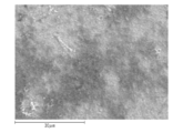
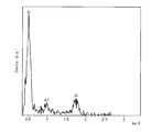
- 2 is an SEM image of a thin film produced in Example 1. It is a figure which shows the measurement result of the composition analysis by EDX of the thin film produced in Example 1.
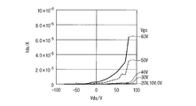
- FIG. 4 is a graph showing measurement results of TFT characteristics of a thin film produced in Example 1.
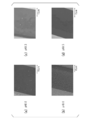
- 6 is a SEM image of a thin film produced in Example 4. It is a figure which shows the measurement result of the composition analysis by EDX of the thin film produced in Example 4.
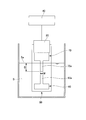
- FIG. 6 shows a TFT wiring structure on a PET substrate manufactured in Example 5.
- 6 is a graph showing measurement results of current / voltage characteristics of TFTs on a PET substrate produced in Example 5.
- Method of manufacturing zinc oxide thin film In the method for producing a zinc oxide thin film of this embodiment, a substrate having a conductive part at least partially is immersed in a solution containing zinc ions, hydroxide ions and zinc complex ions, and an alternating current is applied to the conductive part. This is a method of forming a zinc oxide thin film in a region including a conductive portion on a substrate by energization.
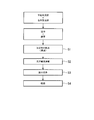
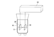
- FIG. 1 and 2A to 2C are explanatory views showing a method of manufacturing a zinc oxide thin film according to the present embodiment.
- FIG. 1 is a flowchart showing a method for producing a zinc oxide thin film.
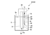
- 2A to 2C are process diagrams showing an example of a method for producing a zinc oxide thin film.
- a solution in which a zinc salt is dissolved (zinc salt solution) and a basic solution are mixed, stirred at room temperature, and then allowed to stand.
- the solvent of the zinc salt solution and the basic solution is not particularly limited as long as each solute can be dissolved.
- Water can be used as a solvent for the zinc salt solution and the basic solution.
- a zinc salt solution prepared using water as a solvent and a basic aqueous solution can be mixed.
- water is used as the solvent.
- the solvent other than water is not particularly limited as long as it can dissolve the solute, and alcohol or the like can also be used.
- zinc salt that is a solute of the zinc salt solution
- a solvent water
- zinc ions Zn 2+
- zinc nitrate, zinc chloride, zinc acetate, zinc citrate, zinc sulfate and the like are used.
- solute of the basic solution one that dissolves in a solvent (water) to generate hydroxide ions (OH ⁇ ) is used.
- a solvent water
- hydroxide ions OH ⁇
- sodium hydroxide, potassium hydroxide, calcium hydroxide, ammonia or the like is used.
- zinc ions (Zn 2+ ) dissolved in the solution are combined with hydroxide ions (OH ⁇ ) to become zinc hydroxide (Zn (OH) 2 ), resulting in a colloidal white precipitate.
- zinc hydroxide which is a white precipitate, binds to hydroxide ions and converts tetrahydroxy zinc (II) acid ions ([Zn (OH) 4 ] 2 ⁇ ). Occurs and dissolves in solution.
- the solution thus obtained is a “basic solution containing tetrahydroxyzinc (II) acid ions”.
- the “basic solution containing tetrahydroxyzinc (II) acid ions” includes zinc ions and hydroxide ions in addition to tetrahydroxyzinc (II) acid ions.
- “basic solution containing tetrahydroxyzinc (II) acid ion” may be referred to as “solution S”.
- the pH of the solution S can be 8 to 12, and preferably 9 to 10. If the pH of the solution S is less than 8, the concentration of hydroxide ions is too low, and tetrahydroxyzinc (II) acid ions are not stably formed in the solution S. In some cases, a thin film made of zinc oxide cannot be formed. On the other hand, when the pH of the solution S exceeds 12, the concentration of hydroxide ions is too high, and the generated zinc oxide thin film may be eluted.
- the addition amount of the basic solution to the zinc salt solution is adjusted.
- acidic solutions such as a zinc salt solution, nitric acid, and hydrochloric acid.
- the pair of base materials 20 and 30 are immersed in the solution S in the container 10 at a predetermined interval, and are formed on the surfaces of the base materials 20 and 30 from the AC power source 40, respectively.
- a zinc oxide thin film is formed in a region including the conductive portions on the substrate surface (step S2).
- the base materials 20 and 30 are members in which a portion having conductivity is provided on at least a part of the surface, and the whole may be made of a conductor such as metal.
- a conductive film having a predetermined pattern may be formed by plating or the like on a glass substrate or a semiconductor substrate on which an insulating layer is formed.
- the electroconductive part provided in the base materials 20 and 30 functions as an anode or a cathode according to the direction through which an electric current flows by sending an alternating current in a solution.
- FIG. 2A the case where the pair of identical base materials 20 and 30 is immersed in the solution is illustrated, but the number of base materials is not limited to this, and two or more pairs of base materials should be used. You can also.
- it may replace with one base material and may use the electrode which consists of an electroconductive member which functions only as a counter electrode at the time of electrolysis, such as a gold electrode and a platinum electrode.
- an alternating current may be passed between the conductive portions of the base materials 20 and 30 while stirring the solution S using a magnetic stirrer or a stirring blade.
- the conductive portions on the base material are a pair of conductive portions arranged to face each other with an insulating gap therebetween, of the pair of conductive portions. If an alternating current is applied to only one conductive part and AC electrolysis is performed, a zinc oxide thin film is formed so as to bridge between the other conductive part. At this time, it is not necessary to specifically control the potential of the other conductive portion, and it may be a floating potential. In other words, the zinc oxide thin film grows by filling the insulating gap so as to bridge between the conductive part to which the alternating current is applied and the conductive part having the floating potential opposed to the conductive part across the insulating gap.
- alternating current electrolysis a pair of electrodes formed on the substrate with a gap therebetween is bridged.
- a zinc oxide thin film having a high purity and a sufficiently large mobility can be formed. Therefore, when a source electrode and a drain electrode are formed on a substrate in advance and an alternating current is applied to at least one of them to perform an alternating current electrolysis, a zinc oxide semiconductor layer is formed between the source electrode and the drain electrode. Can do.
- a thin film transistor can be manufactured by disposing a gate electrode by an appropriate means.
- a zinc oxide thin film is formed only directly on the cathode side electrode. In other words, a thin film transistor structure cannot be obtained because a zinc oxide thin film cannot be formed between the electrodes.
- the temperature of the solution S can be 150 ° C. or less, and preferably 20 to 80 ° C. When the temperature of the solution S exceeds 150 ° C., particulate zinc oxide crystals are precipitated from tetrahydroxyzinc (II) acid ions and may be mixed in the solution S. In addition, since the pH of the solution S decreases with a chemical reaction that precipitates zinc oxide particles, the management of the solution S may be difficult.
- the current density on the film forming surface of the current (electrolytic current) passed between the base materials 20 and 30 immersed in the solution S can be 0.1 to 3 mA / cm 2, and preferably 0.5 to 1. 5 mA / cm 2 .
- the current density of the alternating current is a peak value. If the current density on the surface of the conductive portion (electrode) where zinc oxide is to be deposited is less than 0.1 mA / cm 2 , the desired electrochemical reaction does not occur and the zinc oxide thin film may not be formed. . On the other hand, when the current density exceeds 3 mA / cm 2 , zinc precipitation becomes dominant and the zinc oxide thin film is hardly precipitated.
- the frequency of the alternating current passed between the electrodes can be 0.1 to 10 Hz, and preferably 0.3 to 3 Hz.
- the frequency of the alternating current flowing between the electrodes is less than 0.1 Hz, the switching between the anode and the cathode is too slow, so that the zinc precipitation that occurs at the cathode becomes dominant, the oxidation reaction cannot catch up, and a zinc oxide thin film is formed. There are things you can't do.
- the frequency of the alternating current flowing between the electrodes exceeds 10 Hz, the switching between the anode and the cathode is too early, so that sufficient time for the reaction to occur cannot be obtained, the desired chemical reaction does not occur, and oxidation occurs. A zinc thin film may not be formed.
- one or both of the base materials 20 and 30 are formed on the substrate 51, the insulating film 52 provided on the one surface 51a of the substrate 51, and the one surface 52a of the insulating film 52, as shown in FIG. 2B.
- the base material 50 comprised from the provided source electrode 60 and the drain electrode 70 may be sufficient.
- the source electrode 60 and the drain electrode 70 are provided with a predetermined distance d and are electrically insulated from each other.
- the source electrode and the drain electrode can function as a source electrode and a drain electrode of a thin film transistor by forming a semiconductor layer serving as a channel layer between both electrodes and further appropriately arranging a gate electrode. Refers to the configured electrode.
- the base material 50 is fixed (held) by the conductive clip 80 so as to sandwich the drain electrode 70 and the substrate 51 from the thickness direction of the base material 50.
- the conductive clip 80 is made of a metal having excellent corrosion resistance, such as stainless steel.
- FIG. 2C is a view of the substrate 50 shown in FIG. 2B as viewed from the surface side on which the source electrode 60 and the drain electrode 70 are formed.
- each of the source electrode 60 and the drain electrode 70 has a convex planar shape when viewed from the surface side.
- the source electrode 60 has a rectangular protrusion 60a.
- the drain electrode 70 has a rectangular projection 70a.
- the source electrode 60 and the drain electrode 70 are arranged such that the convex portion 60a of the source electrode 60 and the convex portion 70a of the drain electrode 70 face each other.
- the source electrode width is defined by the width W of the convex portion 60 a of the source electrode 60.
- the drain electrode width is defined by the width W of the convex portion 70 a of the drain electrode 70.
- the electrode width of the source electrode and the electrode width of the drain electrode are W.
- the position of the base material 50 is adjusted so that the end of the convex portion 70a of the drain electrode 70 is located at a depth D from the liquid surface Sa.
- a part of the convex portion 70 a of the drain electrode 70 is immersed in the solution S.
- the thicknesses of the substrate 51 and the insulating film 52 are not particularly limited, and are appropriately adjusted according to required specifications.
- the substrate 51 is not particularly limited, and for example, a glass substrate, a resin film, a silicon substrate, or the like can be used.
- the insulating film 52 is not particularly limited, and a film made of silicon dioxide (SiO 2 ) or aluminum oxide (Al 2 O 3 ) can be used.
- the source electrode 60 and / or the drain electrode 70 may be directly formed on the substrate 51 without providing the insulating film 52 on the substrate 51.
- the source electrode 60 may include a first layer 61 made of chromium (Cr) and a second layer 62 made of gold (Au), which are sequentially stacked on the insulating film 52.
- the thickness of the 1st layer 61 and the 2nd layer 62 is not specifically limited, It adjusts suitably according to the specification etc. which are requested
- the drain electrode 70 may be composed of a first layer 71 made of chromium (Cr) and a second layer 72 made of gold (Au), which are sequentially stacked on the insulating film 52.
- the thickness of the 1st layer 71 and the 2nd layer 72 is not specifically limited, According to the specification etc. which are requested
- the distance d between the source electrode 60 and the drain electrode 70 is not particularly limited, and is appropriately adjusted according to required specifications, but is, for example, 1 ⁇ m to 1000 ⁇ m.
- the insulating film 52 is exposed in the gap 63 between the source electrode 60 and the drain electrode 70, and the gap 63 is a non-conductive part (insulating gap).
- the liquid surface Sa of the solution S is positioned above the gap 63 between the source electrode 60 and the drain electrode 70.
- a zinc oxide thin film (film) is formed in a region including a portion of the drain electrode 70 that is in contact with the solution S. More specifically, a zinc oxide thin film is formed on the insulating film 52 opened in the gap 63 between the source electrode 60 and the drain electrode 70 in addition to the drain electrode 70, and oxidized so as to bridge the source electrode 60 and the drain electrode 70.
- a zinc thin film grows.
- a zinc oxide thin film is also formed on the source electrode 60 that is not connected to an AC power source.
- the source electrode 60 is completely immersed in the solution S, and electrolytic deposition is performed by bringing a part of the drain electrode 70 into contact with the solution S.
- the source electrode 60 and the drain electrode 70 are interchanged. It is good also as arrangement. Further, both the source electrode 60 and the drain electrode 70 may be completely immersed in the solution S.
- the obtained zinc oxide thin film is washed with pure water adjusted to a predetermined temperature to remove impurities contained in the zinc oxide thin film (step S3).
- the temperature of the pure water is not particularly limited, and is about 70 ° C., for example.
- the zinc oxide thin film is obtained by completely drying the zinc oxide thin film (step S4).
- the zinc oxide thin film is formed not only between the source electrode 60 and the drain electrode 70 but also on the source electrode 60 and the drain electrode 70 by electrolytic deposition. It is formed.
- “on the source electrode 60” refers to a surface opposite to the surface in contact with the insulating film 52 of the source electrode 60 and a side surface of the source electrode 60.
- the term “on the drain electrode 70” refers to the surface of the drain electrode 70 opposite to the surface in contact with the insulating film 52 and the side surface of the drain electrode 70.
- a zinc oxide thin film having high purity and sufficiently high mobility can be produced by a non-vacuum and low temperature wet film forming method.
- a zinc oxide thin film can be formed so that a source electrode and a drain electrode may be bridge
- a zinc oxide thin film is formed not only between the source electrode and the drain electrode but also on the non-conductive gate insulating film by electrolytic deposition. Can do.
- the zinc oxide thin film formed so as to bridge between the source electrode and the drain electrode functions as a channel layer of a thin film transistor (TFT).
- the zinc oxide thin film of this embodiment is manufactured by the manufacturing method of the zinc oxide thin film of this embodiment mentioned above.
- the zinc oxide thin film of this embodiment has high purity and has a sufficiently large mobility.
- the zinc oxide thin film of this embodiment can function as a channel layer of a thin film transistor (TFT) when formed so as to bridge between the source electrode and the drain electrode.
- TFT thin film transistor
- the thin film transistor of the present embodiment is obtained by forming a channel layer, a gate insulating layer, a protective insulating layer, an electrode layer, or the like on a substrate made of various types of glass such as quartz glass, a resin film, or a silicon substrate.
- a gate insulating layer consists of a zinc oxide thin film manufactured with the manufacturing method of the zinc oxide thin film of the above-mentioned this embodiment.
- the type of the thin film transistor of this embodiment is not particularly limited, and may be any of a staggered type, an inverted staggered type, a coplanar type, and an inverted coplanar type.
- a thin film transistor having a channel layer made of a zinc oxide thin film manufactured by the method for manufacturing a zinc oxide thin film of the present embodiment described above has a sufficiently large mobility.
- the transparent oxide wiring of the present embodiment is composed of a zinc oxide thin film manufactured by the above-described method for manufacturing a zinc oxide thin film.
- the transparent oxide wiring according to the present embodiment is formed on an insulating substrate made of various types of glass such as quartz glass, a resin film, and the like by the above-described method for manufacturing a zinc oxide thin film according to the present embodiment.
- the insulating substrate includes those in which an insulating layer is formed on a conductive substrate made of metal or the like.
- the shape of the transparent oxide wiring is not particularly limited, and can be formed into an arbitrary shape by adjusting the shape and interval of the electrodes or performing masking as necessary.
- the transparent oxide wiring composed of the zinc oxide thin film manufactured by the method of manufacturing the zinc oxide thin film of the present embodiment described above has high purity and low impurity content, and therefore has low resistance and excellent conductivity.
- a desired gate voltage was applied between the source electrode and the drain electrode by connecting a VOLTAG CURRENT SOURCE (ADVANTEST R6161) to the gate electrode and the source electrode portion.
- Each measuring device was connected to a personal computer via GPIB connection, and various parameters were set and data was taken in by a program created with LabVIEW.
- TFT characteristics were measured using the n-Si substrate itself as a gate electrode.
- Example 1 To 0.01 mol of zinc nitrate hexahydrate, 10 mL of 13 mol / L aqueous ammonia was added to prepare a mixed aqueous solution of zinc nitrate hexahydrate and ammonia. At this time, the temperature was 20 ° C. and the pH was about 11. In addition, an electrode for forming a thin film was prepared. As the substrate, an n-Si wafer was used in which an insulating film made of silicon dioxide (SiO 2 ) having a thickness of 150 nm was formed on one surface by heat treatment.
- SiO 2 silicon dioxide
- a base material for forming a thin film was formed. Note that the distance between the source electrode and the drain electrode was 50 ⁇ m, and the source electrode and the drain electrode had a completely symmetrical shape.
- a pair of the above-mentioned base materials were immersed in the mixed aqueous solution accommodated in the container at a predetermined interval. At this time, a pair of base materials were immersed in the mixed aqueous solution with the drain electrode side up as shown in FIG.
- the frequency of the alternating current supplied between the drain electrodes of the pair of base materials was 1 Hz.
- the film formation time was 60 minutes, and a thin film having a thickness of 50 nm could be formed. This thin film was formed between the source electrode and the drain electrode and on the source electrode and the drain electrode.
- the obtained thin film was washed with pure water at about 70 ° C. to remove impurities contained in the thin film. The thin film was then completely dried.
- FIG. 3 is a 2000 times SEM image of the produced thin film. As shown in FIG. 3, the obtained thin film was found to be uniform.
- FIG. 5 shows the measurement results of TFT characteristics for the zinc oxide thin film formed between the source electrode and the drain electrode. From the results of FIG. 5, it can be seen and estimated that when the gate voltage is 40 V, the drain current is 3 ⁇ A, whereas when the gate voltage is 0 V, a drain current of about 1 / 10,000 is obtained. mobility 0.13cm 2 / V ⁇ s, on / off ratio was 10 4. That is, it was found that the zinc oxide thin film functions as a channel layer of the thin film transistor. Moreover, this mobility is a very high value as what was produced by the wet process of room temperature. The on / off ratio is the ratio between the maximum value and the minimum value of the drain current when the gate voltage is modulated.
- Example 2 A thin film having a thickness of 50 nm was formed between the source electrode and the drain electrode in the same manner as in Example 1 except that the frequency of the alternating current applied between the drain electrodes was 2.5 Hz. About the obtained thin film, the TFT characteristic was measured. The results are shown in Table 1. From the results of Table 1, on / off ratio was confirmed 10 2 about the operation.
- Example 3 A thin film having a thickness of 50 nm was formed between the source electrode and the drain electrode in the same manner as in Example 1 except that the frequency of the alternating current applied between the drain electrodes was 0.5 Hz. About the obtained thin film, the TFT characteristic was measured. The results are shown in Table 1. From the results of Table 1, on / off ratio was confirmed 10 2 about the operation.
- Comparative Example 1 A thin film was formed between the electrodes in the same manner as in Example 1 except that a DC voltage of 5 V was applied between the drain electrodes. However, no thin film was formed between the source electrode and the drain electrode.
- Comparative Example 2 A thin film having a thickness of 50 nm was formed between the source electrode and the drain electrode in the same manner as in Example 1 except that the frequency of the alternating current applied between the drain electrodes was 5 Hz. About the obtained thin film, the TFT characteristic was measured. The results are shown in Table 1. From the results of Table 1, the operation as a TFT could not be confirmed.
- Example 3 A thin film having a thickness of 50 nm between the source electrode and the drain electrode is the same as in Example 1 except that the current density of the alternating current applied between the drain electrodes is 5 mA / cm 2 and the frequency of the alternating current is 1 Hz. Formed. About the obtained thin film, the TFT characteristic was measured. The results are shown in Table 1. From the results of Table 1, the operation as a TFT could not be confirmed. When observed on the electrode, a silver-colored thin film derived from the precipitation of zinc was formed, and it seems that oxidation did not catch up with the precipitation of zinc.
- Example 4" In Example 1, the pH of the mixed aqueous solution was 11, but in this example, electrolytic deposition was performed by changing the pH of the mixed aqueous solution. Conditions other than the pH of the mixed aqueous solution were the same as in Example 1. In this example, the pH of the mixed aqueous solution was adjusted to 8.8, 9.0, 9.3, and 9.5 by adjusting the amount of ammonia water having a concentration of 10 mol / L. In this embodiment, the distance between the source electrode and the drain electrode is set to 35 ⁇ m.
- FIG. 6 is an SEM image of the thin film formed between the source electrode and the drain electrode for each pH.
- the triangular areas visible at both ends of the SEM image are part of the source and drain electrodes, respectively.
- precipitation of fine particles was confirmed at pH 8.8 and pH 9.0.
- FIGS. 6C and 6D the growth of the thin film was confirmed at pH 9.3 and pH 9.5. That is, it was found that as the pH increased, the thin film formation mode shifted from fine particle deposition to thin film growth.
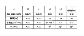
- FIG. 8 shows the state, film thickness, and electrical characteristics of the obtained zinc oxide for the above four types of pH.
- the pH was 9.5, the highest mobility and the largest on / off ratio were obtained.
- Example 5 In the above examples and comparative examples, a Si wafer was used as the substrate.
- a thin film transistor was fabricated on a PET substrate using a PET (Polyethylene Terephthalate) substrate (manufactured by Toyobo Co., Ltd.).
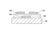
- FIG. 9 shows an element structure before depositing zinc oxide, which is a TFT wiring structure on a PET substrate. The device structure shown in FIG. 9 was fabricated by the following procedure.
- a gate electrode 180 made of NiP / Au having a film thickness of 50 nm was formed on the PET substrate 150 by electroless plating.
- a gate insulating film 190 made of Polyvinyl Phenol (PVP) having a thickness of 1 ⁇ m and an epoxy resin was formed.
- PVP Polyvinyl Phenol
- Commercially available PVP and epoxy resin were used, and a photopolymerization initiator and a solvent were added thereto to obtain a coating solution for forming the gate insulating film 190.
- a spin coat film was formed by spin coating (1000 rpm, 30 seconds) using this coating solution, and pre-baked at 105 ° C. for 30 minutes. Thereafter, UV (ultraviolet) exposure was performed for 30 seconds, followed by 120 ° C. for 30 minutes to form a gate insulating film 190 made of PVP.
- a source electrode 160 and a drain electrode 170 each made of NiP / Au with a film thickness of 50 nm were produced by electroless plating.
- the element structure shown in FIG. 9 was obtained by performing the above processing.
- Example 10 shows current / voltage characteristics of the obtained TFT on the PET substrate. As in the case of the n-Si wafer of Example 4, the operation characteristics as a transistor were obtained. The mobility of this TFT element was 0.3 cm 2 / V ⁇ s, and the on / off ratio was 10 3 .
Landscapes
- Chemical & Material Sciences (AREA)
- Engineering & Computer Science (AREA)
- Chemical Kinetics & Catalysis (AREA)
- Electrochemistry (AREA)
- Materials Engineering (AREA)
- Metallurgy (AREA)
- Organic Chemistry (AREA)
- Inorganic Chemistry (AREA)
- Life Sciences & Earth Sciences (AREA)
- Sustainable Development (AREA)
- Thin Film Transistor (AREA)
- Inorganic Compounds Of Heavy Metals (AREA)
Abstract
酸化亜鉛薄膜の製造方法は、亜鉛イオン、水酸化物イオンおよび亜鉛錯イオンを含む溶液に、少なくとも一部に導電性部位を有する基材を浸漬し、前記導電性部位に交流電流を通電することにより、前記基材上の前記導電性部位を含む領域に酸化亜鉛薄膜を形成する。
Description
本発明は、酸化亜鉛薄膜の製造方法、薄膜トランジスタの製造方法、酸化亜鉛薄膜、薄膜トランジスタおよび透明酸化物配線に関する。
本願は、2012年7月5日に出願された特願2012-151206号に基づき優先権を主張し、その内容をここに援用する。
本願は、2012年7月5日に出願された特願2012-151206号に基づき優先権を主張し、その内容をここに援用する。
酸化亜鉛薄膜は、可視光透過性と電気伝導性を兼ね備えた材料であることから、フラットパネルディスプレー(FPD)や薄膜太陽電池などの透明電極として用いられている。
酸化亜鉛薄膜は、一般的にスパッタリング法などの真空成膜法により成膜される。真空成膜法では、大規模な真空装置を必要とするため、製造コストが高くなる。
より簡便な酸化亜鉛薄膜の成膜方法としては、ゾルゲル法、無電解析出法、電解析出法などの湿式による成膜方法が知られている。これらの方法の中でも、電解析出法を用いた成膜方法としては、亜鉛イオンを含有する水溶液に、導電性基板を浸漬して、その導電性基板に電圧を印加することによって、カソード上に酸化亜鉛薄膜を成膜する方法が知られている(例えば、特許文献1参照)。
酸化亜鉛薄膜は、一般的にスパッタリング法などの真空成膜法により成膜される。真空成膜法では、大規模な真空装置を必要とするため、製造コストが高くなる。
より簡便な酸化亜鉛薄膜の成膜方法としては、ゾルゲル法、無電解析出法、電解析出法などの湿式による成膜方法が知られている。これらの方法の中でも、電解析出法を用いた成膜方法としては、亜鉛イオンを含有する水溶液に、導電性基板を浸漬して、その導電性基板に電圧を印加することによって、カソード上に酸化亜鉛薄膜を成膜する方法が知られている(例えば、特許文献1参照)。
しかしながら、ゾルゲル法では、成膜温度が高く、低温での酸化亜鉛薄膜の成膜が困難であるという問題があった。また、無電解析出法では、一様な膜厚、膜質の酸化亜鉛薄膜を成膜することが難しいという問題があった。一方、電解析出法では、結晶性の高い薄膜を再現性よく、電極上に選択的に成長させることができるものの、導電性を有しない絶縁層上には薄膜が析出しないという問題があった。
このため、薄膜トランジスタのソース・ドレイン間のような電極間の絶縁層上に、電極間を架橋するように酸化亜鉛薄膜を成膜することが難しく、得られた酸化亜鉛薄膜を薄膜トランジスタのチャネル層や配線に利用することが難しかった。
このため、薄膜トランジスタのソース・ドレイン間のような電極間の絶縁層上に、電極間を架橋するように酸化亜鉛薄膜を成膜することが難しく、得られた酸化亜鉛薄膜を薄膜トランジスタのチャネル層や配線に利用することが難しかった。
本発明の態様は、非真空かつ低温、湿式の成膜方法である電解析出法でありながら、薄膜トランジスタのチャネル層や配線に利用可能な酸化亜鉛薄膜を製造することができる酸化亜鉛薄膜の製造方法、薄膜トランジスタの製造方法、酸化亜鉛薄膜、薄膜トランジスタおよび透明酸化物配線を提供することを目的とする。
本発明の第1の態様に従えば、亜鉛イオン、水酸化物イオンおよび亜鉛錯イオンを含む溶液に、少なくとも一部に導電性部位を有する基材を浸漬し、前記導電性部位に交流電流を通電することにより、前記基材上の前記導電性部位を含む領域に酸化亜鉛薄膜を形成する酸化亜鉛薄膜の製造方法が提供される。
本発明の第2の態様に従えば、前記基材が、絶縁間隙を隔てて対向して配置された少なくとも一対の導電性部位を有し、前記交流電流を前記一対の導電性部位のうち一方の導電性部位に通電することにより、前記一対の導電性部位の間を架橋するように酸化亜鉛薄膜を形成する酸化亜鉛薄膜の製造方法が提供される。
本発明の第3の態様に従えば、前記溶液のpHは8~12である酸化亜鉛薄膜の製造方法が提供される。
本発明の第4の態様に従えば、前記溶液の温度は150℃以下である酸化亜鉛薄膜の製造方法が提供される。
本発明の第5の態様に従えば、前記交流電流の周波数は0.1~10Hzである酸化亜鉛薄膜の製造方法が提供される。
本発明の第6の態様に従えば、本発明の第1~5の態様の酸化亜鉛薄膜の製造方法により、基板上に形成されたソース電極とドレイン電極の間を架橋するように酸化亜鉛薄膜を形成する薄膜トランジスタの製造方法が提供される。
本発明の第7の態様に従えば、本発明の第1~5の態様の酸化亜鉛薄膜の製造方法によって製造された酸化亜鉛薄膜が提供される。
本発明の第8の態様に従えば、本発明の第6の態様の薄膜トランジスタの製造方法によって製造された酸化亜鉛薄膜がチャネル層をなす薄膜トランジスタが提供される。
本発明の第9の態様に従えば、本発明の第6の態様の薄膜トランジスタの製造方法によって製造された酸化亜鉛薄膜がゲート絶縁層をなす薄膜トランジスタが提供される。
本発明の第10の態様に従えば、本発明の第1~5の態様の酸化亜鉛薄膜の製造方法によって製造された酸化亜鉛薄膜からなる透明酸化物配線が提供される。
本発明の態様の酸化亜鉛薄膜の製造方法によれば、非真空かつ低温、湿式の成膜方法である電解析出法でありながら、薄膜トランジスタのチャネル層や配線に利用可能な酸化亜鉛薄膜を製造することができる。
以下、図面を参照して、本実施形態に係る酸化亜鉛薄膜の製造方法、酸化亜鉛薄膜、薄膜トランジスタおよび透明酸化物配線について説明する。
なお、以下の全ての図面においては、図面を見やすくするため、各構成要素の寸法や比率などは適宜異ならせている。
また、本実施形態は、発明の趣旨をより良く理解させるために具体的に説明するものであり、特に指定のない限り、本発明を限定するものではない。
なお、以下の全ての図面においては、図面を見やすくするため、各構成要素の寸法や比率などは適宜異ならせている。
また、本実施形態は、発明の趣旨をより良く理解させるために具体的に説明するものであり、特に指定のない限り、本発明を限定するものではない。
「酸化亜鉛薄膜の製造方法」
本実施形態の酸化亜鉛薄膜の製造方法は、亜鉛イオン、水酸化物イオンおよび亜鉛錯イオンを含む溶液に、少なくとも一部に導電性部位を有する基材を浸漬し、導電性部位に交流電流を通電することにより、基材上の導電性部位を含む領域に酸化亜鉛薄膜を形成する方法である。
本実施形態の酸化亜鉛薄膜の製造方法は、亜鉛イオン、水酸化物イオンおよび亜鉛錯イオンを含む溶液に、少なくとも一部に導電性部位を有する基材を浸漬し、導電性部位に交流電流を通電することにより、基材上の導電性部位を含む領域に酸化亜鉛薄膜を形成する方法である。
図1および2A~2Cは、本実施形態に係る酸化亜鉛薄膜の製造方法を示す説明図である。図1は、酸化亜鉛薄膜の製造方法を示すフローチャートである。図2A~2Cは、酸化亜鉛薄膜の製造方法の一例を示す工程図である。
まず、図1に示すように、亜鉛塩を溶解させた溶液(亜鉛塩溶液)と塩基性溶液とを混合し、室温にて攪拌した後、静置する。
亜鉛塩溶液および塩基性溶液の溶媒としては、それぞれの溶質を溶解可能なものであれば特に限定されるものではない。亜鉛塩溶液および塩基性溶液の溶媒として、水を用いることができる。例えば、水を溶媒として調製された亜鉛塩溶液と、塩基性水溶液とを混合することができる。本実施形態においては、溶媒として水を用いる。
なお、水以外の溶媒としては、溶質を溶解可能なものであれば特に限定されず、アルコール等を用いることもできる。
なお、水以外の溶媒としては、溶質を溶解可能なものであれば特に限定されず、アルコール等を用いることもできる。
亜鉛塩溶液の溶質である亜鉛塩としては、溶媒(水)に溶解して亜鉛イオン(Zn2+)を生じるものが用いられる。例えば、硝酸亜鉛、塩化亜鉛、酢酸亜鉛、クエン酸亜鉛、硫酸亜鉛などが用いられる。
塩基性溶液の溶質としては、溶媒(水)に溶解して水酸化物イオン(OH-)を生じるものが用いられる。例えば、水酸化ナトリウム、水酸化カリウム、水酸化カルシウム、アンモニアなどが用いられる。
上記操作により、溶液中に溶解する亜鉛イオン(Zn2+)は、水酸化物イオン(OH-)と結合して水酸化亜鉛(Zn(OH)2)となり、コロイド状の白色沈殿を生じる。
さらに、溶液のpHを8以上とすることで、白色沈殿である水酸化亜鉛は、水酸化物イオンと結合してテトラヒドロキシ亜鉛(II)酸イオン([Zn(OH)4]2-)を生じ、溶液中に溶解する。
さらに、溶液のpHを8以上とすることで、白色沈殿である水酸化亜鉛は、水酸化物イオンと結合してテトラヒドロキシ亜鉛(II)酸イオン([Zn(OH)4]2-)を生じ、溶液中に溶解する。
次いで、溶液に残存する水酸化亜鉛の白色沈殿を、遠心分離機を用いて分離し、上清を採取する(ステップS1)。
このようにして得られた溶液は、「テトラヒドロキシ亜鉛(II)酸イオンを含有する塩基性溶液」である。なお、「テトラヒドロキシ亜鉛(II)酸イオンを含有する塩基性溶液」は、テトラヒドロキシ亜鉛(II)酸イオン以外に、亜鉛イオンや水酸化物イオンを含む。
以下の説明において、「テトラヒドロキシ亜鉛(II)酸イオンを含有する塩基性溶液」を「溶液S」と称することがある。
このようにして得られた溶液は、「テトラヒドロキシ亜鉛(II)酸イオンを含有する塩基性溶液」である。なお、「テトラヒドロキシ亜鉛(II)酸イオンを含有する塩基性溶液」は、テトラヒドロキシ亜鉛(II)酸イオン以外に、亜鉛イオンや水酸化物イオンを含む。
以下の説明において、「テトラヒドロキシ亜鉛(II)酸イオンを含有する塩基性溶液」を「溶液S」と称することがある。
溶液SのpHは、8~12とすることができ、好ましくは9~10である。
溶液SのpHが8未満では、水酸化物イオンの濃度が低すぎて、溶液S中において、テトラヒドロキシ亜鉛(II)酸イオンが安定に形成されず、後述する溶液Sに対する交流電流の通電によって、酸化亜鉛からなる薄膜を形成することができなくなることがある。一方、溶液SのpHが12を超えると、水酸化物イオンの濃度が高すぎて、生成した酸化亜鉛薄膜が溶出してしまうことがある。
溶液SのpHが8未満では、水酸化物イオンの濃度が低すぎて、溶液S中において、テトラヒドロキシ亜鉛(II)酸イオンが安定に形成されず、後述する溶液Sに対する交流電流の通電によって、酸化亜鉛からなる薄膜を形成することができなくなることがある。一方、溶液SのpHが12を超えると、水酸化物イオンの濃度が高すぎて、生成した酸化亜鉛薄膜が溶出してしまうことがある。
溶液SのpHを上記の範囲内に調整するには、亜鉛塩溶液に対する塩基性溶液の添加量を調整する。もしくは、亜鉛塩溶液や硝酸や塩酸といった酸性溶液を添加して調整してもよい。
次いで、図2Aに示すように、容器10内の溶液Sに、所定の間隔を隔てて、一対の基材20,30を浸漬し、交流電源40から、基材20,30の表面にそれぞれ形成された導電性部位間に交流電流を通電することにより、基材表面の導電性部位を含む領域に酸化亜鉛薄膜を形成する(ステップS2)。
なお、基材20,30とは、少なくとも表面の一部に導電性を有する部位が設けられた部材であって、全体が金属などの導電体から構成されていてもよい。また、ガラス基板や表面に絶縁層を形成した半導体基板等に、所定パターンの導電膜がメッキ等により形成されたものであってもよい。
基材20,30に設けられた導電性部位は、溶液中で交流電流を流すことにより、電流の流れる方向によって、アノードまたはカソードとして機能する。
図2Aでは、一対をなす同一形態の基材20,30を溶液中に浸漬する場合を例示したが、基材の数はこれに限定されるものではなく、二対以上の基材を用いることもできる。また、一方の基材に代えて、金電極やプラチナ電極など、単に電解時の対極としてのみ機能する導電性部材からなる電極を用いてもよい。
また、マグネチックスターラーや攪拌翼を用いて、溶液Sを攪拌しながら、基材20,30の導電性部位間に交流電流を通電してもよい。
このとき、アノードでは、下記の化学反応式(1)~(3)で示される化学反応が生じると考えられる。
Zn(OH)4 2- → Zn(OH)2 + 2OH- ・・・(1)
2OH- → 1/2O2 + H2O + 2e- ・・・(2)
Zn(OH)2 → ZnO + H2O ・・・(3)
Zn(OH)4 2- → Zn(OH)2 + 2OH- ・・・(1)
2OH- → 1/2O2 + H2O + 2e- ・・・(2)
Zn(OH)2 → ZnO + H2O ・・・(3)
一方、カソードでは、例えば、下記の化学反応式(4)~(6)で示される化学反応が生じると考えられる。
NO3 - + H2O + 2e- → NO2 - + 2OH- ・・・(4)
Zn2+ + 2OH- → Zn(OH)2 ・・・(5)
Zn(OH)2 → ZnO + H2O ・・・(6)
NO3 - + H2O + 2e- → NO2 - + 2OH- ・・・(4)
Zn2+ + 2OH- → Zn(OH)2 ・・・(5)
Zn(OH)2 → ZnO + H2O ・・・(6)
このように、溶液Sに浸漬した基材20,30間に交流電流を通電することにより、基材20と基材30において、表面の導電性部位でアノード反応(上記の化学反応式(1)~(3)で表される化学反応)とカソード反応(上記の化学反応式(4)~(6)で表される化学反応)がそれぞれ交互に生じて、導電性部位を含む領域に酸化亜鉛薄膜が形成される。
本実施形態の酸化亜鉛薄膜の製造方法によれば、基材上の導電性部位が絶縁ギャップを隔てて対向して配置された一対の導電性部位である場合、その一対の導電性部位のうち片方の導電性部位にのみ交流電流を印加して交流電解すれば、他方の導電性部位との間を架橋するように酸化亜鉛薄膜が形成される。このとき、他方の導電性部位の電位を特別に制御する必要はなく、フローティング電位であっても構わない。
換言すれば、交流電流を印加した導電性部位と、これと絶縁ギャップを隔てて対向するフローティング電位の導電性部位との間を架橋するように、絶縁ギャップを埋めて酸化亜鉛薄膜が成長する。このような現象が生じるメカニズムは明らかではないが、交流電流によってアノード反応とカソード反応が交互に生じることが何らかの原因になっているものと推測される。
本発明者等は、かかる現象を長期にわたる実験研究の結果見出した。この知見に基づいて、絶縁部分を含む領域にも電解析出によって酸化亜鉛薄膜を形成可能な、新たな半導体製造プロセスを提供する。
換言すれば、交流電流を印加した導電性部位と、これと絶縁ギャップを隔てて対向するフローティング電位の導電性部位との間を架橋するように、絶縁ギャップを埋めて酸化亜鉛薄膜が成長する。このような現象が生じるメカニズムは明らかではないが、交流電流によってアノード反応とカソード反応が交互に生じることが何らかの原因になっているものと推測される。
本発明者等は、かかる現象を長期にわたる実験研究の結果見出した。この知見に基づいて、絶縁部分を含む領域にも電解析出によって酸化亜鉛薄膜を形成可能な、新たな半導体製造プロセスを提供する。
本実施形態の交流電流を用いた酸化亜鉛薄膜の形成(以下、「交流電解」と言うことがある。)によれば、基板上に間隔を隔てて形成された一対の電極間を架橋するように、純度が高く、十分に大きな移動度を有する酸化亜鉛薄膜を形成することができる。
したがって、基板上に予めソース電極とドレイン電極を形成しておき、これらの少なくとも一方に交流電流を印加して交流電解を行えば、ソース電極とドレイン電極の間に酸化亜鉛半導体層を形成することができる。さらに、適当な手段によりゲート電極を配置することによって、薄膜トランジスタを製造することができる。
これに対して、公知の直流電解では、カソード側の電極直上にのみ酸化亜鉛薄膜が形成される。換言すれば、電極間に酸化亜鉛薄膜を成膜できないために薄膜トランジスタの構造が得られない。
したがって、基板上に予めソース電極とドレイン電極を形成しておき、これらの少なくとも一方に交流電流を印加して交流電解を行えば、ソース電極とドレイン電極の間に酸化亜鉛半導体層を形成することができる。さらに、適当な手段によりゲート電極を配置することによって、薄膜トランジスタを製造することができる。
これに対して、公知の直流電解では、カソード側の電極直上にのみ酸化亜鉛薄膜が形成される。換言すれば、電極間に酸化亜鉛薄膜を成膜できないために薄膜トランジスタの構造が得られない。
溶液Sの温度は、150℃以下とすることができ、好ましくは20~80℃である。
溶液Sの温度が150℃を超えると、テトラヒドロキシ亜鉛(II)酸イオンから粒子状の酸化亜鉛結晶が析出してしまい、溶液S内に混入することがある。また、酸化亜鉛粒子を析出する化学反応にともなって溶液SのpHが低下するため、溶液Sの管理が困難になることがある。
なお、溶液Sの温度を調節するには、例えば、溶液Sを収容した容器10をホットプレートなどのヒーター上に設置する方法や、溶液Sを収容した容器10をシリコンオイルヒーターに浸漬する方法などが用いられる。
溶液Sの温度が150℃を超えると、テトラヒドロキシ亜鉛(II)酸イオンから粒子状の酸化亜鉛結晶が析出してしまい、溶液S内に混入することがある。また、酸化亜鉛粒子を析出する化学反応にともなって溶液SのpHが低下するため、溶液Sの管理が困難になることがある。
なお、溶液Sの温度を調節するには、例えば、溶液Sを収容した容器10をホットプレートなどのヒーター上に設置する方法や、溶液Sを収容した容器10をシリコンオイルヒーターに浸漬する方法などが用いられる。
溶液Sに浸漬した基材20,30間に通電する電流(電解電流)の成膜面における電流密度は、0.1~3mA/cm2とすることができ、好ましくは0.5~1.5mA/cm2である。ここで、交流電流の電流密度はピーク値である。
酸化亜鉛を析出させようとする導電性部位(電極)の表面における電流密度が0.1mA/cm2未満では、所望の電気化学反応が起こらず、酸化亜鉛薄膜を形成することができないことがある。
一方、電流密度が3mA/cm2を超えると、亜鉛析出が優勢となり、酸化亜鉛薄膜の析出が起こり難くなる。これは、電流密度が大きい場合はカソードでの反応が進み過ぎてしまい、Zn2++2e-→Znという一般的な亜鉛メッキで見られる亜鉛薄膜の析出が優勢となり、酸化亜鉛薄膜の析出を抑制するためと考えられる。
なお、電流密度を上記の範囲内に調整するには、電極間に印加する電圧と、電極間の距離とを調整すればよい。
酸化亜鉛を析出させようとする導電性部位(電極)の表面における電流密度が0.1mA/cm2未満では、所望の電気化学反応が起こらず、酸化亜鉛薄膜を形成することができないことがある。
一方、電流密度が3mA/cm2を超えると、亜鉛析出が優勢となり、酸化亜鉛薄膜の析出が起こり難くなる。これは、電流密度が大きい場合はカソードでの反応が進み過ぎてしまい、Zn2++2e-→Znという一般的な亜鉛メッキで見られる亜鉛薄膜の析出が優勢となり、酸化亜鉛薄膜の析出を抑制するためと考えられる。
なお、電流密度を上記の範囲内に調整するには、電極間に印加する電圧と、電極間の距離とを調整すればよい。
電極間に通電する交流電流の周波数は0.1~10Hzとすることができ、好ましくは0.3~3Hzである。
電極間に通電する交流電流の周波数が0.1Hz未満では、アノードとカソードの切り替えが遅すぎることから、カソードで起こる亜鉛析出が優勢となってしまい、酸化反応が追い付かなくなり、酸化亜鉛薄膜を形成することができないことがある。一方、電極間に通電する交流電流の周波数が10Hzを超えると、アノードとカソードの切り替えが早すぎるために、反応が起こるまでの十分な時間が得られず、所望の化学反応が起こらなくなり、酸化亜鉛薄膜を形成することができないことがある。
電極間に通電する交流電流の周波数が0.1Hz未満では、アノードとカソードの切り替えが遅すぎることから、カソードで起こる亜鉛析出が優勢となってしまい、酸化反応が追い付かなくなり、酸化亜鉛薄膜を形成することができないことがある。一方、電極間に通電する交流電流の周波数が10Hzを超えると、アノードとカソードの切り替えが早すぎるために、反応が起こるまでの十分な時間が得られず、所望の化学反応が起こらなくなり、酸化亜鉛薄膜を形成することができないことがある。
本実施形態では、基材20,30のいずれか一方または両方が、図2Bに示すように、基板51と、基板51の一面51aに設けられた絶縁膜52と、絶縁膜52の一面52aに設けられたソース電極60およびドレイン電極70とから構成される基材50であってもよい。ソース電極60とドレイン電極70は、所定の間隔dを隔てて設けられ、互いに電気的に絶縁されている。
ここで、ソース電極およびドレイン電極とは、両電極間にチャネル層となる半導体層を形成し、さらに、ゲート電極を適切に配置することにより、薄膜トランジスタのソース電極およびドレイン電極として機能しうるように構成されている電極を指す。
また、基材50は、ドレイン電極70と基板51とを、基材50の厚さ方向から挟み込むようにして、導電性クリップ80により固定(保持)されている。導電性クリップ80は、ステンレスなどの耐腐食性に優れる金属から構成されている。
ここで、ソース電極およびドレイン電極とは、両電極間にチャネル層となる半導体層を形成し、さらに、ゲート電極を適切に配置することにより、薄膜トランジスタのソース電極およびドレイン電極として機能しうるように構成されている電極を指す。
また、基材50は、ドレイン電極70と基板51とを、基材50の厚さ方向から挟み込むようにして、導電性クリップ80により固定(保持)されている。導電性クリップ80は、ステンレスなどの耐腐食性に優れる金属から構成されている。
図2Cは、図2Bに示す基材50を、ソース電極60及びドレイン電極70が形成された表面側から見た図である。本実施形態では、ソース電極60及びドレイン電極70のそれぞれは、表面側から見て凸状の平面形状を有する。換言すれば、ソース電極60は、矩形状の凸部60aを有する。ドレイン電極70は、矩形状の凸部70aを有する。ソース電極60とドレイン電極70は、ソース電極60の凸部60aとドレイン電極70の凸部70aが互いに対向するように配置される。
この電極配置の薄膜トランジスタ構造では、ソース電極幅は、ソース電極60の凸部60aの幅Wで規定される。同様に、ドレイン電極幅は、ドレイン電極70の凸部70aの幅Wで規定される。換言すれば、図2Cに示す構造の薄膜トランジスタでは、ソース電極の電極幅及びドレイン電極の電極幅はWである。
図2Cに示すように、基材50の位置は、ドレイン電極70の凸部70aの端が液面Saからの深さDに位置するように調整されている。本実施形態では、ドレイン電極70の凸部70aの一部が、溶液Sに浸漬される。
この電極配置の薄膜トランジスタ構造では、ソース電極幅は、ソース電極60の凸部60aの幅Wで規定される。同様に、ドレイン電極幅は、ドレイン電極70の凸部70aの幅Wで規定される。換言すれば、図2Cに示す構造の薄膜トランジスタでは、ソース電極の電極幅及びドレイン電極の電極幅はWである。
図2Cに示すように、基材50の位置は、ドレイン電極70の凸部70aの端が液面Saからの深さDに位置するように調整されている。本実施形態では、ドレイン電極70の凸部70aの一部が、溶液Sに浸漬される。
基板51と絶縁膜52の厚さは特に限定されるものではなく、要求される仕様などに応じて適宜調整される。
基板51としては、特に限定されるものではなく、例えば、ガラス基板、樹脂フィルム、シリコン基板などを用いることができる。
絶縁膜52としては、特に限定されるものではなく、二酸化ケイ素(SiO2)や酸化アルミニウム(Al2O3)からなる膜などを用いることができる。基板51が絶縁体からなる場合は、基板51上に絶縁膜52を設けずに、ソース電極60および/またはドレイン電極70を基板51上に直接形成してもよい。
基板51としては、特に限定されるものではなく、例えば、ガラス基板、樹脂フィルム、シリコン基板などを用いることができる。
絶縁膜52としては、特に限定されるものではなく、二酸化ケイ素(SiO2)や酸化アルミニウム(Al2O3)からなる膜などを用いることができる。基板51が絶縁体からなる場合は、基板51上に絶縁膜52を設けずに、ソース電極60および/またはドレイン電極70を基板51上に直接形成してもよい。
ソース電極60は、絶縁膜52上に順に積層されたクロム(Cr)からなる第一の層61と、金(Au)からなる第二の層62とから構成されてもよい。第一の層61と第二の層62の厚さは特に限定されるものではなく、要求される仕様などに応じて適宜調整される。
ドレイン電極70は、絶縁膜52上に順に積層されたクロム(Cr)からなる第一の層71と、金(Au)からなる第二の層72とから構成されてもよい。第一の層71と第二の層72の厚さは特に限定されるものではなく、要求される仕様などに応じて適宜調整される。
ドレイン電極70は、絶縁膜52上に順に積層されたクロム(Cr)からなる第一の層71と、金(Au)からなる第二の層72とから構成されてもよい。第一の層71と第二の層72の厚さは特に限定されるものではなく、要求される仕様などに応じて適宜調整される。
ソース電極60とドレイン電極70の間隔dは、特に限定されるものではなく、要求される仕様などに応じて適宜調整されるが、例えば、1μm~1000μmとされる。なお、ソース電極60とドレイン電極70の間隙63には、絶縁膜52が露出しており、間隙63は非導電部位(絶縁ギャップ)となっている。
このような基材20,30を用いる場合、溶液Sの液面Saが、ソース電極60とドレイン電極70の間隙63よりも上に位置するようにする。
ここで、溶液Sに浸漬した基材50のドレイン電極70に交流電流を通電すると、ドレイン電極70の溶液Sに接している部分を含む領域に酸化亜鉛薄膜(皮膜)が形成される。より詳細には、ドレイン電極70の他、ソース電極60とドレイン電極70の間隙63に開口する絶縁膜52上にも酸化亜鉛薄膜が形成され、ソース電極60およびドレイン電極70を架橋するように酸化亜鉛薄膜が成長する。また、交流電源に接続されていないソース電極60上にも酸化亜鉛薄膜が形成される。
上記の実施形態では、ソース電極60を溶液S中に完全に浸漬し、ドレイン電極70の一部を溶液Sに接触させて電解析出を行っているが、ソース電極60とドレイン電極70を入れ替えた配置としてもよい。また、ソース電極60およびドレイン電極70の双方を溶液S中に完全に浸漬させてもよい。
次いで、所定の温度に調整された純水により、得られた酸化亜鉛薄膜を洗浄し、酸化亜鉛薄膜に含まれる不純物を除去する(ステップS3)。
純水の温度は、特に限定されるものではなく、例えば、70℃程度とする。
純水の温度は、特に限定されるものではなく、例えば、70℃程度とする。
次いで、酸化亜鉛薄膜を完全に乾燥させることにより、酸化亜鉛薄膜が得られる(ステップS4)。
なお、本実施形態の酸化亜鉛薄膜の製造方法によれば、電解析出法によって、ソース電極60とドレイン電極70の間のみならず、ソース電極60上やドレイン電極70上にも酸化亜鉛薄膜が形成される。
なお、ソース電極60上とは、ソース電極60の絶縁膜52と接している面とは反対側の面やソース電極60の側面のことである。ドレイン電極70上とは、ドレイン電極70の絶縁膜52と接している面とは反対側の面やドレイン電極70の側面のことである。
なお、本実施形態の酸化亜鉛薄膜の製造方法によれば、電解析出法によって、ソース電極60とドレイン電極70の間のみならず、ソース電極60上やドレイン電極70上にも酸化亜鉛薄膜が形成される。
なお、ソース電極60上とは、ソース電極60の絶縁膜52と接している面とは反対側の面やソース電極60の側面のことである。ドレイン電極70上とは、ドレイン電極70の絶縁膜52と接している面とは反対側の面やドレイン電極70の側面のことである。
本実施形態の酸化亜鉛薄膜の製造方法によれば、非真空かつ低温の湿式の成膜方法により、純度が高く、十分に大きな移動度を有する酸化亜鉛薄膜を製造することができる。
また、本実施形態の酸化亜鉛薄膜の製造方法によれば、電解析出法によって、ソース電極とドレイン電極の間を架橋するように酸化亜鉛薄膜を形成することができる。すなわち、本実施形態の酸化亜鉛薄膜の製造方法によれば、簡便かつ選択的に金属電極間に、酸化亜鉛薄膜を形成することができる。
また、本実施形態の酸化亜鉛薄膜の製造方法によれば、電解析出法によって、ソース電極とドレイン電極の間のみならず、非導電性のゲート絶縁膜上にも酸化亜鉛薄膜を形成することができる。このようにして、ソース電極とドレイン電極の間を架橋するように形成された酸化亜鉛薄膜は、薄膜トランジスタ(TFT)のチャネル層として機能する。
また、本実施形態の酸化亜鉛薄膜の製造方法によれば、電解析出法によって、ソース電極とドレイン電極の間を架橋するように酸化亜鉛薄膜を形成することができる。すなわち、本実施形態の酸化亜鉛薄膜の製造方法によれば、簡便かつ選択的に金属電極間に、酸化亜鉛薄膜を形成することができる。
また、本実施形態の酸化亜鉛薄膜の製造方法によれば、電解析出法によって、ソース電極とドレイン電極の間のみならず、非導電性のゲート絶縁膜上にも酸化亜鉛薄膜を形成することができる。このようにして、ソース電極とドレイン電極の間を架橋するように形成された酸化亜鉛薄膜は、薄膜トランジスタ(TFT)のチャネル層として機能する。
「酸化亜鉛薄膜」
本実施形態の酸化亜鉛薄膜は、上述の本実施形態の酸化亜鉛薄膜の製造方法によって製造される。
本実施形態の酸化亜鉛薄膜は、純度が高く、十分に大きな移動度を有している。また、本実施形態の酸化亜鉛薄膜は、ソース電極とドレイン電極の間を架橋するように形成された場合、薄膜トランジスタ(TFT)のチャネル層として機能することができる。
本実施形態の酸化亜鉛薄膜は、上述の本実施形態の酸化亜鉛薄膜の製造方法によって製造される。
本実施形態の酸化亜鉛薄膜は、純度が高く、十分に大きな移動度を有している。また、本実施形態の酸化亜鉛薄膜は、ソース電極とドレイン電極の間を架橋するように形成された場合、薄膜トランジスタ(TFT)のチャネル層として機能することができる。
「薄膜トランジスタ」
本実施形態の薄膜トランジスタは、石英ガラス等の各種ガラスや樹脂フィルムなどからなる基板やシリコン基板に、チャネル層、ゲート絶縁層、保護絶縁層、電極層などが形成されたものであり、チャネル層またはゲート絶縁層が、上述の本実施形態の酸化亜鉛薄膜の製造方法によって製造された酸化亜鉛薄膜からなるものである。
本実施形態の薄膜トランジスタの種類は、特に限定されるものではなく、スタガード型、インバーテッド・スタガード型、 コープレーナー型、インバーテッド・コープレーナー型のいずれであってもよい。
特に、上述の本実施形態の酸化亜鉛薄膜の製造方法によって製造された酸化亜鉛薄膜からなるチャネル層を有する薄膜トランジスタは、十分に大きな移動度を有するものとなる。
「透明酸化物配線」
本実施形態の透明酸化物配線は、上述の本実施形態の酸化亜鉛薄膜の製造方法によって製造された酸化亜鉛薄膜からなる。
本実施形態の透明酸化物配線は、上述の本実施形態の酸化亜鉛薄膜の製造方法によって、石英ガラス等の各種ガラスや樹脂フィルムなどからなる絶縁性の基板上に形成される。ここで、絶縁性の基板としては、金属製等の導電性基板上に絶縁層を形成したものも含まれる。
なお、透明酸化物配線の形状は、特に限定されるものではなく、電極の形状や間隔を調整したり、必要に応じてマスキングを施すことにより、任意の形状に形成することができる。
上述の本実施形態の酸化亜鉛薄膜の製造方法によって製造された酸化亜鉛薄膜からなる透明酸化物配線は、純度が高く、不純物の含有量が少ないので、抵抗が低く、導電性に優れている。
以下、実施例および比較例により本発明をさらに具体的に説明するが、本発明は以下の実施例に限定されるものではない。
実施例および比較例における物性測定方法は次の通りである。
(表面形状)
走査型電子顕微鏡(SEM)を用いて、得られた酸化亜鉛薄膜の表面形状を観察した。
(膜組成)
エネルギー分散型X線分析法(Energy Dispersive X-ray Spectrometry:EDX)を用いて求めた。
(TFT特性)
ゲート電圧を変化させ、2電極間(ソース-ドレイン)において、2電極間に形成した酸化亜鉛薄膜の電流-電圧測定を行った。±200Vの電圧発生機能を有するDIGITAL ELECTROMETER(ADCMT8252)を、デバイスのソース電極およびドレイン電極に接続し、ソース電極-ドレイン電極間電流(ISD)を計測した。
同時に、VOLTAGE CURRENT SOURCE(ADVANTEST R6161) をゲート電極とソース電極部分に接続することによって、ソース電極-ドレイン電極間に所望のゲート電圧を印加した。
各測定装置は、GPIB接続を介してパソコンへ接続し、LabVIEWで作成したプログラムによって各種パラメータの設定、データの取り込みを行った。
なお、以下の実施例および比較例においては、n-Si基板自体をゲート電極として使用してTFT特性を測定した。
「実施例1」
0.01molの硝酸亜鉛6水和物に対して、13mol/Lのアンモニア水10mLを加えて、硝酸亜鉛6水和物とアンモニアの混合水溶液を調製した。この際、温度は20℃でpHは11程度を示した。
また、薄膜成膜用の電極を用意した。
基板としては、熱処理により、一面に、厚さ150nmの二酸化ケイ素(SiO2)からなる絶縁膜が形成されたn-Siウェハを用いた。
この絶縁膜上に、スパッタリング法により、厚さ5nmのクロムからなる層と厚さ100nmの金からなる層が積層された矩形のソース電極とドレイン電極を、矩形の一辺が対向するように間隔を隔てて形成し、薄膜成膜用の基材を作製した。なお、ソース電極とドレイン電極の間隔は50μmとし、ソース電極とドレイン電極は完全に対称な形状とした。
次いで、20℃において、容器内に収容した混合水溶液に、所定の間隔を隔てて、上記の基材を一対浸漬した。このとき、混合水溶液の液面が、ソース電極とドレイン電極の間隙よりも上になるように、図2Bに示すようにドレイン電極側を上にして、混合水溶液に、一対の基材を浸漬した。ドレイン電極と混合水溶液との接触面積が1cm2となるように、基材の高さを調整した。
この状態で、一対の基材のドレイン電極間に正弦波の交流電圧(ピーク値)を±5V印加した。このとき、ドレイン電極が混合水溶液と接する面における電流密度が1mA/cm2となるように、ドレイン電極間の間隔(距離)を調整した。このとき、ドレイン電極間の間隔(距離)は約1cmであった。また、一対の基材のドレイン電極間に通電する交流電流の周波数を1Hzとした。
基材のドレイン電極間に交流電圧を印加している時間を成膜時間とすると、成膜時間が60分で、厚さ50nmの薄膜を形成することができた。この薄膜は、ソース電極とドレイン電極の間、および、ソース電極上とドレイン電極上に形成されていた。
次いで、70℃程度の純水により、得られた薄膜を洗浄し、薄膜に含まれる不純物を除去した。
次いで、薄膜を完全に乾燥させた。
得られた薄膜を走査型電子顕微鏡(SEM)により観察した。図3は、作製した薄膜の2000倍のSEM像である。図3に示すように、得られた薄膜は一様であることが分かった。
また、ソース電極とドレイン電極の間に形成された薄膜上の点について、EDXによりポイント組成解析を行ったところ、図4に示すように、基板材料であるシリコン(Si)以外の元素として、酸素(O)と亜鉛(Zn)のみが検出された。また、X線回折(XRD)によりZnOの回折ピークが検出され、酸化亜鉛薄膜が形成されていることが分かった。したがって、一対の金属電極を挟んで絶縁体(SiO2膜)の上に、電解析出により酸化亜鉛薄膜を形成することができた。
また、図5に、ソース電極とドレイン電極の間に形成された酸化亜鉛薄膜についてのTFT特性の測定結果を示す。
図5の結果から、ゲート電圧が40Vの場合、ドレイン電流が3μAであるのに対して、ゲート電圧が0Vの場合、10000分の1程度のドレイン電流が得られていることが分かり、見積もられる移動度は0.13cm2/V・s、on/off比は104であった。すなわち、酸化亜鉛薄膜は、薄膜トランジスタのチャネル層として機能していることが分かった。
また、この移動度は、室温の湿式プロセスで作製されたものとしては非常に高い値である。
なお、on/off比とは、ゲート電圧を変調した時のドレイン電流の最大値と最小値の比のことである。
図5の結果から、ゲート電圧が40Vの場合、ドレイン電流が3μAであるのに対して、ゲート電圧が0Vの場合、10000分の1程度のドレイン電流が得られていることが分かり、見積もられる移動度は0.13cm2/V・s、on/off比は104であった。すなわち、酸化亜鉛薄膜は、薄膜トランジスタのチャネル層として機能していることが分かった。
また、この移動度は、室温の湿式プロセスで作製されたものとしては非常に高い値である。
なお、on/off比とは、ゲート電圧を変調した時のドレイン電流の最大値と最小値の比のことである。
「実施例2」
ドレイン電極間に通電する交流電流の周波数を2.5Hzとした以外は実施例1と同様にして、ソース電極とドレイン電極の間に、厚さ50nmの薄膜を形成した。
得られた薄膜について、TFT特性を測定した。結果を表1に示す。
表1の結果から、on/off比が102程度の動作を確認できた。
ドレイン電極間に通電する交流電流の周波数を2.5Hzとした以外は実施例1と同様にして、ソース電極とドレイン電極の間に、厚さ50nmの薄膜を形成した。
得られた薄膜について、TFT特性を測定した。結果を表1に示す。
表1の結果から、on/off比が102程度の動作を確認できた。
「実施例3」
ドレイン電極間に通電する交流電流の周波数を0.5Hzとした以外は実施例1と同様にして、ソース電極とドレイン電極の間に、厚さ50nmの薄膜を形成した。
得られた薄膜について、TFT特性を測定した。結果を表1に示す。
表1の結果から、on/off比が102程度の動作を確認できた。
ドレイン電極間に通電する交流電流の周波数を0.5Hzとした以外は実施例1と同様にして、ソース電極とドレイン電極の間に、厚さ50nmの薄膜を形成した。
得られた薄膜について、TFT特性を測定した。結果を表1に示す。
表1の結果から、on/off比が102程度の動作を確認できた。
「比較例1」
ドレイン電極間に直流電圧を5V印加した以外は実施例1と同様にして、電極間に薄膜の形成を試みた。
しかしながら、ソース電極とドレイン電極の間には薄膜は形成されなかった。
ドレイン電極間に直流電圧を5V印加した以外は実施例1と同様にして、電極間に薄膜の形成を試みた。
しかしながら、ソース電極とドレイン電極の間には薄膜は形成されなかった。
「比較例2」
ドレイン電極間に通電する交流電流の周波数を5Hzとした以外は実施例1と同様にして、ソース電極とドレイン電極の間に、厚さ50nmの薄膜を形成した。
得られた薄膜について、TFT特性を測定した。結果を表1に示す。
表1の結果から、TFTとしての動作を確認できなかった。
ドレイン電極間に通電する交流電流の周波数を5Hzとした以外は実施例1と同様にして、ソース電極とドレイン電極の間に、厚さ50nmの薄膜を形成した。
得られた薄膜について、TFT特性を測定した。結果を表1に示す。
表1の結果から、TFTとしての動作を確認できなかった。
「比較例3」
ドレイン電極間に通電する交流電流の電流密度を5mA/cm2とし、交流電流の周波数を1Hzとした以外は実施例1と同様にして、ソース電極とドレイン電極の間に、厚さ50nmの薄膜を形成した。
得られた薄膜について、TFT特性を測定した。結果を表1に示す。
表1の結果から、TFTとしての動作を確認できなかった。電極上に観測すると亜鉛の析出に由来する銀色の薄膜が形成されており、亜鉛の析出に対して酸化が追い付かなかったものと思われる。
ドレイン電極間に通電する交流電流の電流密度を5mA/cm2とし、交流電流の周波数を1Hzとした以外は実施例1と同様にして、ソース電極とドレイン電極の間に、厚さ50nmの薄膜を形成した。
得られた薄膜について、TFT特性を測定した。結果を表1に示す。
表1の結果から、TFTとしての動作を確認できなかった。電極上に観測すると亜鉛の析出に由来する銀色の薄膜が形成されており、亜鉛の析出に対して酸化が追い付かなかったものと思われる。

「実施例4」
実施例1では、混合水溶液のpHは11であったが、本実施例では、混合水溶液のpHを変化させて電解析出を行った。混合水溶液のpH以外の条件は、実施例1と同じとした。本実施例では、10mol/Lの濃度のアンモニア水の滴下量を調整することで、混合水溶液のpHを、8.8、9.0、9.3、9.5に調整した。また、本実施例ではソース電極とドレイン電極の間隔を35μmとした。
実施例1では、混合水溶液のpHは11であったが、本実施例では、混合水溶液のpHを変化させて電解析出を行った。混合水溶液のpH以外の条件は、実施例1と同じとした。本実施例では、10mol/Lの濃度のアンモニア水の滴下量を調整することで、混合水溶液のpHを、8.8、9.0、9.3、9.5に調整した。また、本実施例ではソース電極とドレイン電極の間隔を35μmとした。
図6は、それぞれのpHについて、ソース電極とドレイン電極との間に形成された薄膜のSEM像である。SEM像の両端に見える三角形の領域はそれぞれソース電極とドレイン電極の一部である。図6(a)、6(b)に示すように、pH8.8及びpH9.0では微粒子の析出が確認された。一方、図6(c)、6(d)に示すように、pH9.3、pH9.5では、薄膜の成長が確認された。つまり、pHの増加に伴い、薄膜の形成モードが微粒子析出から薄膜成長へと移行していることがわかった。
pHが9.5の場合に、ソース電極とドレイン電極との間に形成された薄膜上の一点について、EDXによりポイント組成解析を行った。その結果、図7に示すように、基板材料であるシリコン(Si)以外の元素として、酸素(O)と亜鉛(Zn)のみが検出された。また、XRDにより、酸化亜鉛(ZnO)の回折ピークが検出された。EDX及びXRDの結果から、酸化亜鉛の薄膜が形成されていることが分かった。
図8に、上記4種類のpHに関して、得られた酸化亜鉛の状態、膜厚、及び電気特性を示す。pHが9.5の場合に、最も高い移動度と最も大きいon/off比が得られた。
「実施例5」
上記の実施例及び比較例では、基板としてSiウェハを用いた。実施例5では、基板としてPET(Polyethylene Terephthalate)基板((株)東洋紡製)を用い、PET基板上への薄膜トランジスタの作製を行った。
図9は、PET基板上のTFT用配線構造であって、酸化亜鉛を析出させる前の素子構造を示す。図9の素子構造は以下の手順で作製した。
上記の実施例及び比較例では、基板としてSiウェハを用いた。実施例5では、基板としてPET(Polyethylene Terephthalate)基板((株)東洋紡製)を用い、PET基板上への薄膜トランジスタの作製を行った。
図9は、PET基板上のTFT用配線構造であって、酸化亜鉛を析出させる前の素子構造を示す。図9の素子構造は以下の手順で作製した。
まず、PET基板150上に、膜厚50nmのNiP/Auからなるゲート電極180を無電解めっきで作製した。
次に、膜厚1μmのPolyvinyl Phenol(PVP)とエポキシ樹脂からなるゲート絶縁膜190を形成した。PVPとエポキシ樹脂には市販のものを用い、これらに光重合開始剤と溶媒を加えてゲート絶縁膜190を形成するための塗布液を得た。
次に、膜厚1μmのPolyvinyl Phenol(PVP)とエポキシ樹脂からなるゲート絶縁膜190を形成した。PVPとエポキシ樹脂には市販のものを用い、これらに光重合開始剤と溶媒を加えてゲート絶縁膜190を形成するための塗布液を得た。
この塗布液を用いたスピンコート(1000rpm、30秒)により、スピンコート膜を成膜し、105oC30分間のプリベークを行った。その後、UV(Ultraviolet)露光を30秒間行い、続いて120oC30分間のアニールを行って、PVPからなるゲート絶縁膜190を形成した。
次に、それぞれが膜厚50nmのNiP/Auからなるソース電極160及びドレイン電極170を無電解めっきで作製した。
以上の処理を行うことで、図9に示す素子構造を得た。
以上の処理を行うことで、図9に示す素子構造を得た。
上記の素子構造に対し、TFTのチャネル層を形成するために、酸化亜鉛薄膜の電解析出を行った。混合水溶液のpHは、実施例4で最も高い性能のTFTが得られた9.5に設定した。混合水溶液のpH以外の条件は、実施例1と同じとした。
図10は、得られたPET基板上TFTの電流・電圧特性である。実施例4のn-Siウェハ上の場合と同様に、トランジスタとしての動作特性が得られた。このTFT素子の移動度は0.3cm2/V・s、on/off比は103であった。
図10は、得られたPET基板上TFTの電流・電圧特性である。実施例4のn-Siウェハ上の場合と同様に、トランジスタとしての動作特性が得られた。このTFT素子の移動度は0.3cm2/V・s、on/off比は103であった。
20,30・・・基材、40・・・交流電源、50・・・基材、51・・・基板、60・・・ソース電極、70・・・ドレイン電極、80・・・導電性クリップ。
Claims (10)
- 亜鉛イオン、水酸化物イオンおよび亜鉛錯イオンを含む溶液に、少なくとも一部に導電性部位を有する基材を浸漬し、前記導電性部位に交流電流を通電することにより、前記基材上の前記導電性部位を含む領域に酸化亜鉛薄膜を形成することを特徴とする酸化亜鉛薄膜の製造方法。
- 前記基材が、絶縁間隙を隔てて対向して配置された少なくとも一対の導電性部位を有し、前記交流電流を前記一対の導電性部位のうち一方の導電性部位に通電することにより、前記一対の導電性部位の間を架橋するように酸化亜鉛薄膜を形成することを特徴とする請求項1に記載の酸化亜鉛薄膜の製造方法。
- 前記溶液のpHは8~12である、請求項1または2に記載の酸化亜鉛薄膜の製造方法。
- 前記溶液の温度は150℃以下である、請求項1~3のいずれか1項に記載の酸化亜鉛薄膜の製造方法。
- 前記交流電流の周波数は0.1~10Hzである、請求項1~4のいずれか1項に記載の酸化亜鉛薄膜の製造方法。
- 請求項1~5のいずれか1項に記載の酸化亜鉛薄膜の製造方法により、基板上に形成されたソース電極とドレイン電極の間を架橋するように酸化亜鉛薄膜を形成することを特徴とする薄膜トランジスタの製造方法。
- 請求項1~5のいずれか1項に記載の酸化亜鉛薄膜の製造方法によって製造されたことを特徴とする酸化亜鉛薄膜。
- 請求項6に記載の薄膜トランジスタの製造方法によって製造された酸化亜鉛薄膜がチャネル層をなすことを特徴する薄膜トランジスタ。
- 請求項6に記載の薄膜トランジスタの製造方法によって製造された酸化亜鉛薄膜がゲート絶縁層をなすことを特徴する薄膜トランジスタ。
- 請求項1~5のいずれか1項に記載の酸化亜鉛薄膜の製造方法によって製造された酸化亜鉛薄膜からなることを特徴する透明酸化物配線。
Priority Applications (3)
| Application Number | Priority Date | Filing Date | Title |
|---|---|---|---|
| CN201380033284.8A CN104428453B (zh) | 2012-07-05 | 2013-07-02 | 氧化锌薄膜的制造方法、薄膜晶体管的制造方法、氧化锌薄膜、薄膜晶体管和透明氧化物配线 |
| JP2014523752A JP6060972B2 (ja) | 2012-07-05 | 2013-07-02 | 酸化亜鉛薄膜の製造方法、薄膜トランジスタの製造方法および透明酸化物配線の製造方法 |
| US14/570,191 US9337320B2 (en) | 2012-07-05 | 2014-12-15 | Method of manufacturing zinc oxide thin film, method of manufacturing thin film transistor, zinc oxide thin film, thin film transistor, and transparent oxide wiring |
Applications Claiming Priority (2)
| Application Number | Priority Date | Filing Date | Title |
|---|---|---|---|
| JP2012151206 | 2012-07-05 | ||
| JP2012-151206 | 2012-07-05 |
Related Child Applications (1)
| Application Number | Title | Priority Date | Filing Date |
|---|---|---|---|
| US14/570,191 Continuation US9337320B2 (en) | 2012-07-05 | 2014-12-15 | Method of manufacturing zinc oxide thin film, method of manufacturing thin film transistor, zinc oxide thin film, thin film transistor, and transparent oxide wiring |
Publications (1)
| Publication Number | Publication Date |
|---|---|
| WO2014007250A1 true WO2014007250A1 (ja) | 2014-01-09 |
Family
ID=49882004
Family Applications (1)
| Application Number | Title | Priority Date | Filing Date |
|---|---|---|---|
| PCT/JP2013/068136 Ceased WO2014007250A1 (ja) | 2012-07-05 | 2013-07-02 | 酸化亜鉛薄膜の製造方法、薄膜トランジスタの製造方法、酸化亜鉛薄膜、薄膜トランジスタおよび透明酸化物配線 |
Country Status (4)
| Country | Link |
|---|---|
| US (1) | US9337320B2 (ja) |
| JP (1) | JP6060972B2 (ja) |
| CN (1) | CN104428453B (ja) |
| WO (1) | WO2014007250A1 (ja) |
Families Citing this family (2)
| Publication number | Priority date | Publication date | Assignee | Title |
|---|---|---|---|---|
| KR101812698B1 (ko) * | 2015-08-28 | 2018-01-30 | 전북대학교산학협력단 | 금속 산화물이 성장된 탄소섬유 제조 방법 |
| CN114695821A (zh) * | 2020-12-31 | 2022-07-01 | Tcl科技集团股份有限公司 | 量子点发光二极管的制备方法 |
Citations (5)
| Publication number | Priority date | Publication date | Assignee | Title |
|---|---|---|---|---|
| JP2005171271A (ja) * | 2003-12-08 | 2005-06-30 | Canon Inc | 堆積膜の形成方法、それを用いた光起電力素子の製造方法 |
| JP2008547195A (ja) * | 2005-06-16 | 2008-12-25 | イーストマン コダック カンパニー | 亜鉛酸化物をベースとした半導体材料を含む薄膜トランジスタ |
| WO2009081807A1 (ja) * | 2007-12-21 | 2009-07-02 | Kansai Paint Co., Ltd. | 表面処理された金属基材の製造方法及び該製造方法により得られた表面処理された金属基材、並びに金属基材処理方法及び該方法によって処理された金属基材 |
| WO2011135514A2 (en) * | 2010-04-28 | 2011-11-03 | Basf Se | Process for preparing a zinc complex in solution |
| JP2012036482A (ja) * | 2010-08-11 | 2012-02-23 | Univ Of Tsukuba | シアノ架橋金属錯体作成方法およびエレクトロクロミック素子 |
Family Cites Families (11)
| Publication number | Priority date | Publication date | Assignee | Title |
|---|---|---|---|---|
| DE69123555T2 (de) * | 1990-10-01 | 1997-05-28 | Sharp Kk | Verfahren zur Herstellung von Überzügen aus supraleitendem Oxyd |
| EP0794270B1 (en) * | 1996-03-06 | 2000-06-14 | Canon Kabushiki Kaisha | Process for production of zinc oxide thin film, and process for production of semiconductor device substrate and process for production of photoelectric conversion device using the same film |
| JP3499106B2 (ja) * | 1997-03-03 | 2004-02-23 | 富士通株式会社 | 配線の形成方法及び配線基板 |
| JP3327811B2 (ja) | 1997-05-13 | 2002-09-24 | キヤノン株式会社 | 酸化亜鉛薄膜の製造方法、それを用いた光起電力素子及び半導体素子基板の製造方法 |
| JP4445711B2 (ja) * | 2002-04-19 | 2010-04-07 | 株式会社Kri | 金属酸化物パターン形成方法及び金属配線パターン形成方法 |
| US20060096867A1 (en) * | 2004-11-10 | 2006-05-11 | George Bokisa | Tin alloy electroplating system |
| JP5089139B2 (ja) * | 2005-11-15 | 2012-12-05 | 株式会社半導体エネルギー研究所 | 半導体装置の作製方法 |
| JP4977478B2 (ja) * | 2006-01-21 | 2012-07-18 | 三星電子株式会社 | ZnOフィルム及びこれを用いたTFTの製造方法 |
| KR100959460B1 (ko) * | 2007-11-16 | 2010-05-25 | 주식회사 동부하이텍 | 투명 박막 트랜지스터 및 투명 박막 트랜지스터의 제조방법 |
| JP5291928B2 (ja) * | 2007-12-26 | 2013-09-18 | 株式会社日立製作所 | 酸化物半導体装置およびその製造方法 |
| TW201016596A (en) * | 2008-09-04 | 2010-05-01 | Univ Kumamoto Nat Univ Corp | Method of manufacturing zinc oxide nanoparticles and zinc oxide nanoparticles |
-
2013
- 2013-07-02 CN CN201380033284.8A patent/CN104428453B/zh active Active
- 2013-07-02 JP JP2014523752A patent/JP6060972B2/ja active Active
- 2013-07-02 WO PCT/JP2013/068136 patent/WO2014007250A1/ja not_active Ceased
-
2014
- 2014-12-15 US US14/570,191 patent/US9337320B2/en active Active
Patent Citations (5)
| Publication number | Priority date | Publication date | Assignee | Title |
|---|---|---|---|---|
| JP2005171271A (ja) * | 2003-12-08 | 2005-06-30 | Canon Inc | 堆積膜の形成方法、それを用いた光起電力素子の製造方法 |
| JP2008547195A (ja) * | 2005-06-16 | 2008-12-25 | イーストマン コダック カンパニー | 亜鉛酸化物をベースとした半導体材料を含む薄膜トランジスタ |
| WO2009081807A1 (ja) * | 2007-12-21 | 2009-07-02 | Kansai Paint Co., Ltd. | 表面処理された金属基材の製造方法及び該製造方法により得られた表面処理された金属基材、並びに金属基材処理方法及び該方法によって処理された金属基材 |
| WO2011135514A2 (en) * | 2010-04-28 | 2011-11-03 | Basf Se | Process for preparing a zinc complex in solution |
| JP2012036482A (ja) * | 2010-08-11 | 2012-02-23 | Univ Of Tsukuba | シアノ架橋金属錯体作成方法およびエレクトロクロミック素子 |
Also Published As
| Publication number | Publication date |
|---|---|
| JPWO2014007250A1 (ja) | 2016-06-02 |
| US9337320B2 (en) | 2016-05-10 |
| JP6060972B2 (ja) | 2017-01-18 |
| CN104428453B (zh) | 2017-04-05 |
| CN104428453A (zh) | 2015-03-18 |
| US20150187916A1 (en) | 2015-07-02 |
Similar Documents
| Publication | Publication Date | Title |
|---|---|---|
| Salim et al. | Electrodeposition of CdTe thin films using nitrate precursor for applications in solar cells | |
| Xin et al. | Synthesis of CuS thin films by microwave assisted chemical bath deposition | |
| Prabukanthan et al. | Photovoltaic device performance of pure, manganese (Mn2+) doped and irradiated CuInSe2 thin films | |
| Zhen et al. | Liquid metal-embraced photoactive films for artificial photosynthesis | |
| Yamaguchi et al. | Mechanistic study of chemical deposition of ZnS thin films from aqueous solutions containing zinc acetate and thioacetamide by comparison with homogeneous precipitation | |
| El-rouby et al. | Electrical, electrochemical and photo-electrochemical studies on the electrodeposited n-type semiconductor hexagonal crystalline CdS thin film on nickel substrate | |
| CN109545960B (zh) | 一种电导连续可变的忆阻器及其制备方法和应用 | |
| Spada et al. | Role of acidic and basic electrolytes on the structure and morphology of cathodically reduced indium tin oxide (ITO) substrates | |
| Keikhaei et al. | Fabrication of Mg (OH) 2 thin films by electrochemical deposition with Cu catalyst | |
| Osial et al. | Influence of electrodeposition conditions on the properties of CdTe films | |
| Prabukanthan et al. | Structural, morphological, electrocatalytic activity and photocurrent properties of electrochemically deposited FeS2 thin films | |
| Basu et al. | Nanoporous ZnO thin films deposited by electrochemical anodization: effect of UV light | |
| Shpaisman et al. | Electrochemical synthesis of morphology-controlled segmented CdSe nanowires | |
| Lee et al. | Spontaneously polarized lithium-doped zinc oxide nanowires as photoanodes for electrical water splitting | |
| Ait Layachi et al. | Pulsed potential co-electrodeposition of Cu2CoSnS4 absorber layer on fluorinated tin oxide (FTO)-coated glass | |
| CN104087976A (zh) | Sm-Co合金非晶磁性纳米线阵列的制备方法 | |
| JP6060972B2 (ja) | 酸化亜鉛薄膜の製造方法、薄膜トランジスタの製造方法および透明酸化物配線の製造方法 | |
| Trzciński et al. | Controlling crystallites orientation and facet exposure for enhanced electrochemical properties of polycrystalline MoO3 films | |
| Liu et al. | Dimensionally anisotropic graphene with high mobility and a high on–off ratio in a three-terminal RRAM device | |
| Florica et al. | Field effect transistor with electrodeposited ZnO nanowire channel | |
| CN103489899A (zh) | 氧化物半导体的前体组合物、薄膜晶体管基板及其制法 | |
| Dhanasekaran et al. | Electrochemical and physical properties of electroplated CuO thin films | |
| Luo et al. | Synthesis of CdTe thin films on flexible metal foil by electrodeposition | |
| Feng et al. | Fabrication of WO3 photoanode on crystalline Si solar cell for water splitting | |
| Yun et al. | Selective area hydrothermal growth of ZnO nanowires for application to electrochemical sensor |
Legal Events
| Date | Code | Title | Description |
|---|---|---|---|
| 121 | Ep: the epo has been informed by wipo that ep was designated in this application |
Ref document number: 13812980 Country of ref document: EP Kind code of ref document: A1 |
|
| ENP | Entry into the national phase |
Ref document number: 2014523752 Country of ref document: JP Kind code of ref document: A |
|
| NENP | Non-entry into the national phase |
Ref country code: DE |
|
| 122 | Ep: pct application non-entry in european phase |
Ref document number: 13812980 Country of ref document: EP Kind code of ref document: A1 |