WO2014002363A1 - 放射線検出器及びその製造方法 - Google Patents
放射線検出器及びその製造方法 Download PDFInfo
- Publication number
- WO2014002363A1 WO2014002363A1 PCT/JP2013/002976 JP2013002976W WO2014002363A1 WO 2014002363 A1 WO2014002363 A1 WO 2014002363A1 JP 2013002976 W JP2013002976 W JP 2013002976W WO 2014002363 A1 WO2014002363 A1 WO 2014002363A1
- Authority
- WO
- WIPO (PCT)
- Prior art keywords
- radiation detector
- manufacturing
- scintillator layer
- partition
- substrate
- Prior art date
- Legal status (The legal status is an assumption and is not a legal conclusion. Google has not performed a legal analysis and makes no representation as to the accuracy of the status listed.)
- Ceased
Links
Images


Classifications
-
- G—PHYSICS
- G01—MEASURING; TESTING
- G01T—MEASUREMENT OF NUCLEAR OR X-RADIATION
- G01T1/00—Measuring X-radiation, gamma radiation, corpuscular radiation, or cosmic radiation
- G01T1/16—Measuring radiation intensity
- G01T1/20—Measuring radiation intensity with scintillation detectors
- G01T1/2002—Optical details, e.g. reflecting or diffusing layers
Definitions
- This technology relates to a radiation detector used for radiography such as medical treatment and nondestructive inspection, and a manufacturing method thereof.
- the radiation inspection apparatus described in Patent Document 1 includes a scintillator layer provided on an output substrate, and a partition wall structure section provided on the scintillator layer, which partitions a plurality of pixels.
- the partition provided in the partition structure part is formed to a predetermined height by repeating screen printing a plurality of times.
- a scintillator layer is formed by filling the partition wall with a phosphor (see, for example, paragraph [0044] of Patent Document 1).
- the flat detector described in Patent Document 2 also includes a scintillator layer formed on the photoelectric conversion substrate and a partition that partitions the scintillator layer for each pixel.
- the partition walls are formed by, for example, a screen printing method, a resist patterning method, or a photosensitive paste method (pattern exposure of a photosensitive paste partition shape, development and baking treatment thereof) (for example, a paragraph in the specification of Patent Document 2) [0047], [0052] to [0056], [0064]).
- An object of the present technology is to provide a radiation detector that achieves high radiation sensitivity and a method for manufacturing the same.
- a radiation detector includes a sensor substrate, a scintillator layer, and a partition wall.
- the sensor substrate has a plurality of pixels capable of receiving light.
- the scintillator layer is provided on the sensor substrate.
- the partition wall has a height of 300 ⁇ m or more and 800 ⁇ m or less and a width of 10 ⁇ m or more and 40 ⁇ m or less, and is provided so as to partition the scintillator layer for each pixel.
- the volume of the scintillator layer can be increased. That is, radiation can be efficiently converted into visible light, and high sensitivity can be realized.
- the main component of the partition wall material may be an inorganic material.
- the partition wall material may contain 60 wt% or more and 100 wt% or less of glass. Accordingly, the partition walls can be formed with a high aspect ratio by a photolithography technique using a photosensitive material including glass.
- the inorganic material contained in the partition may contain at least one of glass and ceramic.
- the scintillator layer may include a phosphor material and a resin material.
- the resin material By including the resin material, the cured resin can prevent the phosphor material from dropping off in the manufacturing process of the radiation detector.
- the scintillator layer may include a phosphor layer formed of the phosphor material, and a mixed layer disposed between the phosphor layer and the sensor substrate and including both the phosphor material and the resin material. Good.
- the mixed layer containing the resin material on the side closer to the sensor substrate than the phosphor layer, the mixed layer functions as a cap (cover) layer that covers the phosphor layer with the dried or cured resin. To do. Thereby, dropping off of the phosphor material that may occur in the manufacturing process of the radiation detector can be prevented.
- the scintillator layer may include a phosphor material and a glass material. Also with the glass material, it is possible to prevent the phosphor material from falling off during the manufacturing process of the radiation detector.
- the scintillator layer may include a phosphor material.
- the radiation detector may further include a cap layer provided between the scintillator layer and the partition wall and the sensor substrate. By providing the cap layer, it is possible to prevent the phosphor material from falling off during the manufacturing process of the radiation detector.
- the cap layer may include at least a resin material.
- the cap layer may include a material obtained by mixing the phosphor material and the resin material.
- the manufacturing method of the radiation detector which concerns on this technique includes forming a partition on a board
- the partition wall having a high height and a small width is formed as described above, whereby the volume of the scintillator layer can be increased. That is, radiation can be efficiently converted into visible light, and high sensitivity can be realized.
- the “substrate” according to the present technology may be a sensor substrate having a plurality of pixels capable of receiving light, or may be a counter substrate facing the sensor substrate.
- the photosensitive paste material may contain an inorganic material and an organic binder. By substantially removing the organic binder by the above baking, the partition wall made of an inorganic material can be formed.
- the partition may be formed to correspond to a plurality of pixels.
- the manufacturing method further includes a step of bonding the sensor substrate and the substrate so that a scintillator layer made of the scintillator material is disposed on the sensor substrate having the plurality of pixels capable of receiving light. May be.
- the substrate may be a counter substrate facing the sensor substrate having the plurality of pixels capable of receiving light.
- the partition is formed to correspond to a plurality of pixels.
- the manufacturing method may further include a step of bonding the sensor substrate and the counter substrate so that a scintillator layer made of the scintillator material is disposed on the sensor substrate.
- the manufacturing method may further include a step of applying or transferring a material including at least a resin material on the scintillator layer formed by filling the scintillator material.
- a solution containing the resin material may be applied on the scintillator layer.
- a sheet material containing the resin material may be transferred onto the scintillator layer.
- a paste material containing a phosphor material and the resin material may be applied on the scintillator layer.
- the substrate may be a sensor substrate having a plurality of pixels that can receive light.
- the partition is formed to correspond to the plurality of pixels.
- the manufacturing method includes a step of applying or transferring a material containing at least a resin material on the scintillator layer formed by filling the scintillator material on the sensor substrate, and applying or transferring the material.
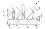
- FIG. 1 shows a part of a cross-sectional structure of a radiation detector according to an embodiment of the present technology.
- 2 is a cross-sectional view taken along line AA in FIG.
- FIG. 3 schematically shows an example of a pixel portion in the sensor substrate and a pixel driving circuit arranged in the peripheral region.
- FIG. 4 shows an example of a circuit of the pixel PX driven by the pixel driving circuit shown in FIG.
- FIG. 5 is a flowchart showing a manufacturing method of the radiation detector according to the present embodiment.
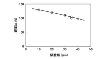
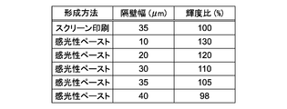
- FIG. 6 is a graph showing the relationship between the width of the partition wall and the luminance (luminance ratio) obtained by the radiation detector having the partition wall of that width.
- FIG. 7 is a table showing the relationship of FIG. FIG.
- FIG. 8 is a graph showing the relationship between the height of the partition and the luminance (luminance ratio) obtained by the radiation detector having the partition of that height.
- FIG. 9 is a table showing the relationship of FIG. FIG. 10 shows a radiation detector according to Example 1 of another embodiment.
- FIG. 11 is a diagram for explaining a method of manufacturing the radiation detector shown in FIG.
- FIG. 12 is a flowchart showing a manufacturing method of the radiation detector shown in FIG.
- FIG. 13 is a diagram for explaining a manufacturing method of the radiation detector according to Example 2 of another embodiment.
- FIG. 14 is a diagram for explaining a manufacturing method of the radiation detector according to Example 3 of another embodiment.
- FIG. 15 is a diagram for explaining a manufacturing method of the radiation detector according to Example 4 of another embodiment.
- FIG. 16 is a diagram for explaining a manufacturing method of the radiation detector according to Example 5 of another embodiment.
- FIG. 17 is a flowchart showing a manufacturing method of the radiation detector shown in FIG.
- FIG. 1 shows a part of a cross-sectional structure of a radiation detector according to an embodiment of the present technology.
- 2 is a cross-sectional view taken along line AA in FIG.
- the radiation detector 1 is a panel that converts radiation represented by ⁇ -rays, ⁇ -rays, ⁇ -rays, and X-rays into visible light, and receives image information based on the radiation as an electrical signal. It is suitably used as an X-ray imaging apparatus for other nondestructive inspection such as baggage inspection.
- the radiation detector 1 includes a sensor substrate 11, a scintillator layer 12 provided on the sensor substrate 11, a partition wall 14 provided on the scintillator layer 12, and a counter substrate (substrate) 13 provided on the scintillator layer 12. With. Hereinafter, the configuration of each unit will be described in detail.
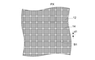
- the sensor substrate 11 has a pixel portion (a pixel portion 10 described later) composed of a plurality of pixels PX that can receive light.
- the sensor substrate 11 is configured such that a drive circuit for driving the pixel unit 10 is disposed in a peripheral region of the pixel unit 10.
- the pixel unit 10 includes a switching element (a transistor Tr described later) such as a TFT (Thin Film Transistor) and a photodiode 16 that is a photoelectric sensor for each pixel as shown in FIG.
- a switching element a transistor Tr described later
- TFT Thin Film Transistor
- the thickness of the sensor substrate 11 is preferably 50 to 1000 ⁇ m from the viewpoint of durability and weight reduction. Details (pixel circuit and cross-sectional structure) of the pixel portion 10 in the sensor substrate 11 and the configuration of the peripheral circuit (pixel drive circuit) will be described later.
- the scintillator layer 12 is a layer composed of a radiation phosphor that emits fluorescence when irradiated with radiation.
- the scintillator material that is the material of the scintillator layer 12 includes at least a phosphor material.
- As the phosphor material a material that absorbs radiation energy and has a high conversion efficiency from, for example, an electromagnetic wave having a wavelength of 300 nm to 800 nm (an electromagnetic wave (light) ranging from ultraviolet light to infrared light centering on visible light) is desirable.
- the scintillator layer can be formed by applying a paste material containing phosphor particles mainly composed of Gd 2 O 2 S, for example.
- Examples of such phosphor materials include those using, for example, CsI as a main agent, and activator (activator) for supplementing luminous efficiency, for example, Tl or Na.
- the thickness of the scintillator layer 12 is, for example, 300 ⁇ m to 800 ⁇ m (300 ⁇ m or more and 800 ⁇ m or less).
- the phosphor material used for the scintillator layer 12 is not limited to the above CsI and Tl.
- An alkali metal halide phosphor represented by the following formula may be used.
- M I represents at least one alkali metal selected from the group consisting of lithium (Li), Na, potassium (K), rubidium (Rb), and Cs.
- M II is comprised of beryllium (Be), magnesium (Mg), calcium (Ca), strontium (Sr), barium (Ba), nickel (Ni), copper (Cu), zinc (Zn) and cadmium (Cd) Represents at least one alkaline earth metal or divalent metal selected from the group;
- M III is scandium (Sc), yttrium (Y), lanthanum (La), cerium (Ce), praseodymium (Pr), neodymium (Nd), promethium (Pm), samarium (Sm), europium (Eu), gadolinium (Gd), terbium (Tb), dysprosium (Dy), holmium (Ho), erbium (Er), thulium (Tm), ytterbium (Yb), lutetium (Lu), aluminum (Al), gallium (Ga) and indium It represents at least one rare earth element or trivalent metal selected from the group consisting of (In).
- X, X ′ and X ′′ each represent at least one halogen element selected from the group consisting of fluorine (F), chlorine (Cl), bromine (Br) and iodine (I).
- A is composed of Y, Ce, Pr, Nd, Sm, Eu, Gd, Tb, Dy, Ho, Er, Tm, Yb, Lu, Na, Mg, Cu, silver (Ag), Tl, and bismuth (Bi). It represents at least one rare earth element or metal selected from the group.
- A, b, and z represent numerical values in the range of 0 ⁇ a ⁇ 0.5, 0 ⁇ b ⁇ 0.5, and 0 ⁇ z ⁇ 1.0, respectively.
- M I preferably contains at least Cs, and X preferably contains at least I.
- A is particularly preferably Tl or Na.
- z is preferably 1 ⁇ 10 ⁇ 4 ⁇ z ⁇ 0.1.
- Basic composition formula (II): M II FX: zLn A rare earth activated alkaline earth metal fluorohalide phosphor represented by the following formula may be used.
- M II represents at least one alkaline earth metal selected from the group consisting of Ba, Sr and Ca.
- Ln represents at least one rare earth element selected from the group consisting of Ce, Pr, Sm, Eu, Tb, Dy, Ho, Nd, Er, Tm, and Yb.
- X represents at least one halogen element selected from the group consisting of Cl, Br and I.
- Z is 0 ⁇ z ⁇ 0.2.
- Ln is particularly preferably Eu or Ce.
- LnTaO 4 (Nb, Gd), Ln 2 SiO 5 : Ce, LnOX: Tm (Ln is a rare earth element), ZnWO 4 , LuAlO 3 : Ce, Gd 3 Ga 25 O 12 : Cr, Ce, HfO 2 and the like.
- the partition 14 is provided so as to partition the scintillator layer 12 for each pixel corresponding to a plurality of pixels. That is, one area surrounded by the partition walls 14 provided in a matrix form in the vertical and horizontal directions is an area corresponding to one pixel PX provided in the sensor substrate 11. Alternatively, one region surrounded by the partition wall 14 may be a region corresponding to a plurality of pixels PX provided on the sensor substrate 11. Hereinafter, an area corresponding to each pixel PX in the scintillator layer 12 is referred to as a pixel corresponding area. As shown in FIG. 1, the photodiode 16 is disposed immediately below the pixel corresponding region.
- the material of the partition wall 14 contains an inorganic material as a main component. Or the material of the partition 14 may be only an inorganic material. Examples of the inorganic material include at least one of glass and ceramic.
- the material of the partition 14 contains 60 wt% or more and 100 wt% or less of glass. When the glass content is less than 60% by weight, the strength of the partition wall 14 is lowered, so that it is desirable that the glass content is 60% by weight or more.
- the material of the partition wall 14 only needs to contain both glass and ceramic.
- silicate glass or borate glass is used as the glass.
- components that can be contained in the glass also, SiO 2, Al 2 O 3 , B 2 O 3, ZnO, BaO, Bi 2 O 3, Li 2 O 3, Na 2 O, K 2 O, PdO, MgO, CaO BaO, SrO, TiO 2 , ZrO 2 and the like.
- TiO 2 ⁇ ZnO, ZrO ⁇ BaSO 4 ⁇ BaCO 3 ⁇ BaTiO 3 ⁇ MgO ⁇ Pb x O y ⁇ PbTiO 3 ⁇ ZnS, or the like is used.
- the size (width d1 and height d2) of the partition 14 shown in FIGS. 1 and 2 will be described later.
- the counter substrate 13 is a glass plate having a thickness of 1 mm or less, for example, and seals the scintillator layer 12 from the upper surface to prevent moisture from entering the scintillator layer 12.
- the side surface of the counter substrate 13 may be provided with a resin coating for improving impact resistance (preventing cracks caused by microcracks), and reflection between the counter substrate 13 and the scintillator layer 12.
- Other layers such as a film may be laminated.
- the material of the counter substrate 13 may be other than glass.
- As the material Al, Cu, Fe, carbon plate, carbon fiber reinforced resin sheet, Si, Ge, GaAs, SiC, SiN, quartz, sapphire, PET, PEN, polycarbonate, polyimide film, or the like is used.
- FIG. 3 schematically illustrates an example of the pixel unit 10 in the sensor substrate 11 and a pixel driving circuit disposed in the peripheral region thereof.
- the circuit unit 15 for driving the pixel unit 10 is disposed around the pixel unit 10.
- pixels (unit pixels) PX including photodiodes 16 and transistors are arranged in a matrix.
- Each pixel PX is connected to a pixel drive line 27 (specifically, a row selection line) and a signal line 28.
- the circuit unit 15 includes, for example, a row scanning unit 23, a column scanning unit 25, and a system control unit 26.
- the row scanning unit 23 includes a shift register, an address decoder, and the like, and drives the pixel unit 10 in units of rows by supplying a drive signal to the pixel unit 10 through the pixel drive line 27.
- the column scanning unit 25 is configured by a shift register, an address decoder, and the like. The column scanning section 25 sequentially receives signals output from the signal lines according to the amount of light received by the photodiodes 16 provided in the respective pixels PX, and outputs these signals to the outside.
- the circuit portion including the row scanning unit 23, the column scanning unit 25, and the horizontal signal line 29 may be a circuit integrated on the sensor substrate 11, or an external control IC connected to the sensor substrate 11. It may be arranged. In addition, these circuit portions may be formed on another substrate connected by a cable or the like.
- the system control unit 26 receives a clock given from the outside, data for instructing an operation mode, and the like, and outputs data such as internal information of the radiation detector 1.
- the system control unit 26 also includes a timing generator that generates various timing signals, and drives the row scanning unit 23 and the column scanning unit 25 based on the various timing signals generated by the timing generator. Control.
- FIG. 4 shows an example of a circuit (pixel circuit 20) of the pixel PX driven by the pixel driving circuit shown in FIG.
- the pixel circuit 20 is a circuit that employs, for example, a passive matrix driving method, and includes a photodiode 16, a capacitor 138, and a transistor Tr.
- the photodiode 16 is a device that generates a signal charge having a charge amount corresponding to the amount of incident light (amount of received light).
- the photodiode 16 and the capacitance component 138 are connected in parallel to the supply line 174 for the reference potential Vxref. That is, the photodiode 16 is connected between the supply line 174 and the storage node N that is one end of the capacitor 138.
- a row operation signal (read signal) Vread is supplied to the row selection line 27.
- the gate of the transistor Tr is connected to the row selection line 27, and the source and drain are connected to the storage node N and the signal line 28, respectively.
- a voltage corresponding to the row operation signal Vread is applied to the gate of the transistor Tr, a signal charge having a charge amount corresponding to the amount of light received by the photodiode 16 accumulated in the capacitor 138 passes through the accumulation node N. It is output to the signal line 28.
- FIG. 5 is a flowchart showing a method for manufacturing the radiation detector according to the present embodiment.
- a reflective film (reflective layer) (not shown) is formed on the counter substrate 13 (step 101).
- a glass paste (a material in which glass particles, ceramic particles, an organic binder, and an organic solvent are mixed) is applied onto the counter substrate 13 by a blade coater to form the reflective film.
- the thickness of the reflective film is, for example, 30 ⁇ m.
- the organic solvent may not be used, and a glass paste to which other additive components are added may be used.
- the counter substrate 13 on which the reflective film is formed is dried (step 102).
- a heat treatment is performed at a temperature of 80 ° C. for about 10 minutes.
- the object is fired (step 103).
- this baking treatment the organic binder contained in the glass paste is removed. This baking process is, for example, about 10 minutes at a temperature of 550 ° C.
- a photosensitive paste is applied as a material constituting the partition wall 14 (step 104).
- the photosensitive paste is a material in which glass particles and a photosensitive organic binder are mixed.
- a photosensitive paste to which an organic solvent or other additive components are added may be used.
- Additive components include, for example, photopolymerization initiators, ultraviolet light absorbers, sensitizers, sensitizers, polymerization inhibitors, plasticizers, thickeners, antioxidants, or dispersant precipitation inhibitors. is there.
- the object is dried (step 105).
- heat treatment is performed at a temperature of 80 ° C. for about 60 minutes.
- the photosensitive paste is patterned into the shape of the partition wall 14 as shown in FIGS. 1 and 2 by exposure processing and development processing of the photosensitive paste material using a photomask (steps 106 and 107).
- the photosensitive paste material contains at least one inorganic material of the glass and ceramic described above for constituting the partition.
- the object is dried (step 108).
- a heat treatment is performed at a temperature of 120 ° C. for about 60 minutes.
- the object is fired (step 109).
- this baking treatment the organic binder contained in the photosensitive paste is removed.
- the baking process is performed at a temperature of 550 ° C. for about 30 minutes.
- the partition wall 14 having the following width d1 is obtained.
- the width d1 of the partition wall 14 is 10 ⁇ m to 40 ⁇ m, more preferably 10 ⁇ m to 30 ⁇ m. If the width d1 of the partition wall 14 is smaller than 10 ⁇ m, the formation becomes difficult. If the width d1 is larger than 40 ⁇ m, the aperture ratio (the aperture ratio for each pixel PX) and the resolution cannot be set to desired design values.
- the width of the partition wall 14 means a width at a half position of the height d2 of the partition wall 14.
- the aspect ratio of the partition wall 14 configured as described above is 10 to 20, 10 to 27, or 30 to 80.
- the manufacturing method according to the present embodiment uses a photolithography technique using a photosensitive paste material containing an inorganic material such as glass for forming the partition wall 14, thereby reducing the width as described above.
- a partition wall having a high aspect ratio can be formed.
- the partition wall 14 having the above size can be formed by one or two exposure and development processes.
- the photolithographic technique using the photosensitive paste the position accuracy and size accuracy of the partition wall 14 are greatly improved.
- the phosphor material that is, the material constituting the scintillator layer 12 is filled in the region surrounded by the barrier ribs 14 (step 110).
- the phosphor material for example, a powder paste prepared by mixing Gd 2 O 2 S: Tb powder, an organic binder and an organic solvent is used. The organic solvent may not be used in some cases.
- This powder paste is applied by a blade coater.
- the coating thickness of the phosphor material is about the same as or higher than the height of the partition wall 14.
- a drying process for example, approximately 80 minutes at 80 ° C.
- a baking process for example, approximately 30 minutes at 500 ° C.
- the surface of the object opposite to the side on which the counter substrate 13 is provided is polished (step 113).
- the excess phosphor material mainly remaining on the surface is removed.
- the height of the partition wall 14 and the scintillator material is substantially the same and constant within the surface. There may be no polishing treatment.
- An adhesive is applied to the polished surface (step 114).
- the adhesive a material in which an organic solvent is mixed in an organic binder is used.
- the coating thickness is 25 ⁇ m, for example, and the adhesive is applied by a blade coater. Thereafter, a drying process (for example, about 5 minutes at 80 ° C.) is performed (step 115). There is no need to apply the adhesive.
- the above-described sensor substrate 11 is prepared, and this sensor substrate 11 is bonded to the counter substrate 13 provided with the scintillator layer 12 and the partition wall 14 (step 116). In this case, both substrates are bonded so that the regions of the plurality of pixels PX provided on the sensor substrate 11 correspond to the pixel corresponding regions of the scintillator layer 12.
- FIG. 6 is a graph showing the relationship between the width (d1) of the partition and the luminance (luminance ratio) obtained by the radiation detector having the partition of that width.
- FIG. 7 is a table showing the relationship.
- the brightness when a partition wall having a width of 35 ⁇ m and a height of 400 ⁇ m is formed by screen printing is set to 100%, and this is the brightness when the partition wall 14 is formed using the photosensitive paste of the present technology.
- the height of the partition was set to 400 ⁇ m.
- FIG. 8 is a graph showing the relationship between the height (d2) of the partition and the luminance (luminance ratio) obtained by the radiation detector having the partition of that height.
- FIG. 9 is a table showing the relationship.
- the brightness when the height of the partition wall is 150 ⁇ m is 100%, and this is compared with the brightness when the partition wall 14 is formed using the photosensitive paste of the present technology.
- the width of the partition wall was set to 30 ⁇ m.
- the higher the height the greater the amount of scintillator material in the pixel-corresponding region, so the amount of radiation absorbed and the saturation point exists.
- the light emission amount that is, the luminance increases.
- the luminance decreases when the predetermined height is exceeded. The inventors believe that the optimum height range is 300 ⁇ m to 800 ⁇ m.
- the volume of the scintillator layer 12 can be increased by providing the partition wall 14 having a high height and a narrow width like the partition wall 14 according to the present embodiment. That is, radiation, here X-rays, can be efficiently converted into visible light, and high sensitivity can be realized.
- FIG. 10 shows a radiation detector according to Example 1.
- the radiation detector 51 includes a sensor substrate 11, a counter substrate 13, a partition wall 14, and a scintillator layer 52.
- the scintillator layer 52 includes a phosphor layer 521 formed of a phosphor material, and a mixed layer 522 including both the phosphor material and the resin material.
- the mixed layer 522 is provided between the phosphor layer 521 and the sensor substrate 11.
- the height of the partition wall 14 is 300 ⁇ m to 800 ⁇ m as described above. 400 ⁇ m to 600 ⁇ m.
- the size of the partition wall 14 can be similarly applied to embodiments according to Examples 2 to 4 described later.
- the thickness of the mixed layer is desirably 10 ⁇ m to 200 ⁇ m.
- FIG. 11 is a diagram for explaining a method of manufacturing the radiation detector shown in FIG.
- FIG. 12 is a flowchart showing the manufacturing method.
- Steps 101 to 112 or 113 in FIG. 5 are executed.
- a scintillator layer 521 'made of a phosphor material is formed.
- a solution 522 'obtained by dissolving a resin material in an organic solvent to form a liquid is applied onto the scintillator layer 521' (step 210).
- the resin material itself may be applied instead of the solution.
- step 210 the mixed layer 522 having the predetermined thickness as described above is formed by adjusting the flow rate of the solution 522 'discharged from the nozzle 40, the moving speed of the nozzle 40, and the like.
- the resin material examples include nitrified cotton, cellulose acetate, ethyl cellulose, polyvinyl butyral, cotton-like polyester, polyvinyl acetate, vinyl chloride, vinylidene chloride, vinyl chloride copolymer, vinylidene chloride-vinyl chloride copolymer, vinyl chloride-vinyl acetate copolymer, Polyalkyl (meth) acrylate, polycarbonate, polyurethane, cellulose acetate butyrate, epoxy, silicone, polyolefin, polyester, polyamide rubber (gum arabic), urethane-modified polyester, gelatin, dextran, nitrocellulose, polyalkyl methacrylate, or polyvinyl Alcohol etc. are mentioned.
- organic solvent for example, methanol, ethanol, propanol, methyl ethyl ether, acetone, MEK, MIBK, butyl acetate, ethyl acetate, ethyl ether, xylene, toluene and the like are used.
- a dispersant such as phthalic acid and stearic acid, and a plasticizer such as triphenyl phosphate and diethyl phthalate may be added to the organic solvent.
- the mixed layer is formed by subjecting the target substrate to be processed (the counter substrate 13 on which the partition wall 14 and the scintillator layer 52 are formed) to drying or curing as described above. (Step 211). Then, the sensor substrate 11 and the target substrate are bonded together so that the scintillator layer 52 is disposed on the sensor substrate 11.
- the solution containing the resin material is applied onto the scintillator layer 521 ′, so that the mixed layer 522 containing the resin material functions as a cap layer in the scintillator layer after the resin is dried or cured. . That is, by providing the cap layer, it is possible to prevent the phosphor material from dropping off that may occur during the manufacturing process of the radiation detector 51.
- FIG. 13 is a diagram for explaining the method of manufacturing the radiation detector according to the second example.
- a region 62 in the partition 14 formed on the counter substrate 13 is filled with a material 62 ′ including both a phosphor material and a resin material, and firing after the filling (for example, Since the “firing” corresponding to step 112 in FIG. 5 is not performed, the resin material remains without being removed and distributed in the scintillator layer 62 as a whole.
- This resin material may be the resin material mentioned in Example 1 above.
- the phosphor material When the resin material is dried or cured, the phosphor material can be prevented from falling off.
- a sensor substrate (not shown) is bonded to the counter substrate 13.
- FIG. 14 is a view for explaining the method for manufacturing the radiation detector according to the third example.
- the region 72 ′ formed on the counter substrate 13 is filled with a material 72 ′ including both a phosphor material and a glass material (for example, glass particles). This is then fired.
- the state and content of the glass can be appropriately adjusted depending on conditions such as the firing temperature and time.
- a sensor substrate (not shown) is bonded to the counter substrate 13.
- FIG. 15 is a diagram for explaining the method of manufacturing the radiation detector according to the fourth example.
- a region in the partition wall 14 formed on the counter substrate 13 is filled with a phosphor material.
- a sheet 82 containing a resin material is transferred onto the partition wall 14 and the scintillator layer 12.
- the sheet 82 functions as a cap layer provided between the scintillator layer 12 and the partition wall 14 and a sensor substrate (not shown).
- the thickness of the sheet is, for example, 10 ⁇ m to 100 ⁇ m.
- the sheet for example, it is roughly divided into a hot-melt adhesive sheet and an adhesive sheet (adhesive sheet).
- the hot melt adhesive sheet include polyolefin, polyester, or polyamide.
- Adhesive sheets include acrylic, polyurethane, silicone, rubber (gum arabic), polyester, urethane-modified polyester, gelatin, dextran, polyvinyl butyral, polyvinyl acetate, nitrocellulose, ethyl cellulose, vinylidene chloride, vinyl chloride copolymer, polyalkylmeta. Examples thereof include acrylate, vinyl chloride, vinyl acetate copolymer, cellulose acetate butyrate, polyvinyl alcohol, and linear polyester.
- the cap layer is formed simply by sticking the sheet 81 to the target substrate, and therefore the cap layer can be easily manufactured.
- FIG. 16 is a diagram for explaining the method of manufacturing the radiation detector according to the fifth example.
- FIG. 17 is a flowchart showing the manufacturing method.
- a paste material 92 in which a phosphor material and a resin material are mixed is applied onto the partition wall 14 and the scintillator layer 12.
- a cap layer is formed.
- a sheet (not shown) containing a phosphor material and a resin material may be transferred onto the partition wall 14 and the scintillator layer 12. Thereafter, drying or curing is performed (step 311).
- the height of the partition wall 14 is 200 ⁇ m to 600 ⁇ m.
- the thickness of the cap layer is desirably 50 ⁇ m to 300 ⁇ m. More desirably, the thickness is 150 ⁇ m to 300 ⁇ m.
- the resin material examples include nitrified cotton, cellulose acetate, ethyl cellulose, polyvinyl butyral, cotton-like polyester, polyvinyl acetate, vinyl chloride, vinylidene chloride, vinyl chloride copolymer, vinylidene chloride-vinyl chloride copolymer, vinyl chloride-vinyl acetate copolymer, Polyalkyl (meth) acrylate, polycarbonate, polyurethane, cellulose acetate butyrate, epoxy, silicone, polyolefin, polyester, polyamide rubber (gum arabic), urethane-modified polyester, gelatin, dextran, nitrocellulose, polyalkyl methacrylate, or polyvinyl Alcohol etc. are mentioned.
- organic solvent for example, methanol, ethanol, propanol, methyl ethyl ether, acetone, MEK, MIBK, butyl acetate, ethyl acetate, ethyl ether, xylene, toluene and the like are used.
- a dispersant such as phthalic acid and stearic acid, and a plasticizer such as triphenyl phosphate and diethyl phthalate may be added to the organic solvent.
- the cap layer containing only the resin material is provided on the scintillator layer as in the embodiment according to Example 4 above, the luminance may be lowered.
- the cap layer according to this embodiment according to Example 5 includes the phosphor material, it is possible to prevent the phosphor material from falling off without reducing the luminance.
- Examples 1 to 5 may be appropriately selected according to the design.
- the partition wall is formed on the counter substrate side.
- the partition wall is formed on the sensor substrate side, and then the sensor substrate on which the partition wall is formed and the counter substrate may be bonded together.
- the partition wall is formed on the sensor substrate side, the counter substrate may not be provided. In that case, the reflective layer is formed on the side opposite to the sensor substrate.
- the partition wall and the scintillator layer may be formed on the sensor substrate side.
- the counter substrate and the sensor substrate may be bonded together.
- the sensor substrate and the counter substrate are bonded together so that the scintillator layer to which the material including at least the resin material is applied or transferred as described above is disposed on the counter substrate.
- the counter substrate may not be provided.
- the scintillator layer was formed by filling and firing the phosphor material in steps 110 to 112.
- the phosphor material may be filled in the region surrounded by the partition walls by vapor deposition through the deposition mask having the partition pattern.
- the temperature and time for drying, baking, and the like can be changed as appropriate.
- glass and ceramic are given as examples of the inorganic material of the photosensitive paste, but other materials may be used.
- the height of the partition wall 14 is not limited to 300 to 800 ⁇ m and 400 to 600 ⁇ m as described above. It may be 300-600 ⁇ m, 300-500 ⁇ m, 300-450 ⁇ m, 300-400 ⁇ m, 400-700 ⁇ m, 450-650 ⁇ m, or 450-700 ⁇ m, 500-700 ⁇ m, or 500-600 ⁇ m.
- the thickness of the partition wall 14 can range from 10 ⁇ m to 40 ⁇ m, 10 ⁇ m to 35 ⁇ m, or 10 ⁇ m to 30 ⁇ m, 20 to 40 ⁇ m, 20 to 35 ⁇ m, 20 to 30 ⁇ m, as described above. .
- the glass transition temperature of the glass used for the counter substrate according to each of the above embodiments may be, for example, 600 ° C. or higher. This is because the heat resistance of the sensor and the substrate is taken into consideration in the manufacturing process.
- the glass transition temperature may be 600 ° C. or higher as described above.
- the specific gravity of the substrate may be 2.4 g / cm 3 or less and the thickness may be 0.5 mm to 1.0 mm, but is not limited to these values.
- the thermal expansion coefficient on the sensor substrate 11 side may be within a range of ⁇ 20% with respect to that of the glass substrate. This is for suppressing the positional deviation between the sensor and the scintillator due to the difference between the thermal expansion coefficients being too large.
- the average diameter of the powder particle may be 5 ⁇ m to 15 ⁇ m. This is because when the diameter is smaller than 5 ⁇ m, a desired luminance cannot be obtained, and when the diameter is larger than 15 ⁇ m, it is difficult to fill the partition wall 14. Further, the melting point of the phosphor material may be 600 ° C. or less in the manufacturing process as described above.
- the present technology can be configured as follows. (1) a sensor substrate having a plurality of pixels capable of receiving light; A scintillator layer provided on the sensor substrate; A radiation detector comprising: a partition wall having a height of 300 ⁇ m or more and 800 ⁇ m or less and a width of 10 ⁇ m or more and 40 ⁇ m or less and provided to partition the scintillator layer for each pixel. (2) The radiation detector according to (1), A radiation detector in which a main component of the material of the partition wall is an inorganic material. (3) The radiation detector according to (2), The inorganic material contained in the partition includes at least one of glass and ceramic. (4) The radiation detector according to (2) or (3), The material of the said partition contains 60 to 100 weight% of glass of radiation detectors.
- the scintillator layer includes a phosphor material and a resin material.
- the radiation detector according to (5), The scintillator layer is A phosphor layer formed of the phosphor material; A radiation detector that is disposed between the phosphor layer and the sensor substrate and includes a mixed layer that includes both the fluorescent material and the resin material.
- the radiation detector according to any one of (1) to (4), The scintillator layer includes a phosphor material and a glass material.
- the scintillator layer includes a phosphor material;
- the radiation detector further includes a cap layer provided between the scintillator layer, the partition wall, and the sensor substrate.
- the cap layer includes at least a resin material.
- the radiation detector according to (9), The cap layer includes a material obtained by mixing the phosphor material and the resin material.
- a partition wall is formed on the substrate by exposure processing and development processing of the photosensitive paste material using a photomask, By firing the substrate on which the partition walls are formed, the partition walls having a height of 300 ⁇ m to 800 ⁇ m and a width of 10 ⁇ m to 40 ⁇ m are formed, A method of manufacturing a radiation detector, comprising filling a scintillator material in a region surrounded by the partition on the substrate after the baking. (12) A method of manufacturing the radiation detector according to (11), The said photosensitive paste material contains an inorganic material and an organic binder. The manufacturing method of the radiation detector.
- the substrate is a counter substrate facing a sensor substrate having a plurality of pixels capable of receiving light;
- the partition is formed to correspond to the plurality of pixels,
- a method of manufacturing a radiation detector further comprising: bonding the sensor substrate and the counter substrate so that a scintillator layer made of the scintillator material is disposed on the sensor substrate.
- coating process applies the solution containing the said resin material on the said scintillator layer.
- a method of manufacturing the radiation detector according to (14), The said transfer process transfers the sheet material containing the said resin material on the said scintillator layer.
- coating process applies the paste material containing fluorescent substance material and the said resin material on the said scintillator layer.
- the substrate is a sensor substrate having a plurality of pixels capable of receiving light;
- a method of manufacturing the radiation detector according to (18), Applying or transferring a material containing at least a resin material on the scintillator layer formed by filling the scintillator material on the sensor substrate; A step of bonding the sensor substrate and the counter substrate so that the scintillator layer coated or transferred with the material is disposed on the counter substrate.
Landscapes
- Physics & Mathematics (AREA)
- Health & Medical Sciences (AREA)
- Life Sciences & Earth Sciences (AREA)
- General Physics & Mathematics (AREA)
- High Energy & Nuclear Physics (AREA)
- Molecular Biology (AREA)
- Spectroscopy & Molecular Physics (AREA)
- Measurement Of Radiation (AREA)
- Conversion Of X-Rays Into Visible Images (AREA)
Applications Claiming Priority (4)
| Application Number | Priority Date | Filing Date | Title |
|---|---|---|---|
| JP2012142132 | 2012-06-25 | ||
| JP2012-142132 | 2012-06-25 | ||
| JP2012-201790 | 2012-09-13 | ||
| JP2012201790A JP6182840B2 (ja) | 2012-06-25 | 2012-09-13 | 放射線検出器の製造方法 |
Publications (1)
| Publication Number | Publication Date |
|---|---|
| WO2014002363A1 true WO2014002363A1 (ja) | 2014-01-03 |
Family
ID=49782565
Family Applications (1)
| Application Number | Title | Priority Date | Filing Date |
|---|---|---|---|
| PCT/JP2013/002976 Ceased WO2014002363A1 (ja) | 2012-06-25 | 2013-05-09 | 放射線検出器及びその製造方法 |
Country Status (2)
| Country | Link |
|---|---|
| JP (1) | JP6182840B2 (https=) |
| WO (1) | WO2014002363A1 (https=) |
Families Citing this family (14)
| Publication number | Priority date | Publication date | Assignee | Title |
|---|---|---|---|---|
| JP6515958B2 (ja) * | 2012-06-25 | 2019-05-22 | ソニー株式会社 | 放射線検出器及びその製造方法 |
| US11597877B2 (en) | 2013-01-21 | 2023-03-07 | Siemens Medical Solutions Usa, Inc. | Passivation of metal halide scintillators |
| US11098248B2 (en) | 2013-01-21 | 2021-08-24 | Siemens Medical Solutions Usa, Inc. | Passivation of metal halide scintillators |
| US10087367B2 (en) | 2013-01-21 | 2018-10-02 | Siemens Medical Solutions Usa, Inc. | Passivation of metal halide scintillators |
| EP3073493A4 (en) * | 2013-11-20 | 2017-07-05 | Toray Industries, Inc. | Scintillator panel |
| US10393887B2 (en) * | 2015-07-19 | 2019-08-27 | Afo Research, Inc. | Fluorine resistant, radiation resistant, and radiation detection glass systems |
| EP3193337A1 (en) * | 2016-01-13 | 2017-07-19 | Siemens Medical Solutions USA, Inc. | Passivation of metal halide scintillators |
| JP6781868B2 (ja) * | 2016-03-24 | 2020-11-11 | 国立大学法人静岡大学 | 放射線検出素子の製造方法 |
| CN109328035B (zh) | 2016-06-15 | 2022-05-10 | 株式会社岛津制作所 | 放射线摄影装置 |
| WO2018020555A1 (ja) * | 2016-07-25 | 2018-02-01 | 野洲メディカルイメージングテクノロジー株式会社 | シンチレータセンサ基板及びシンチレータセンサ基板の製造方法 |
| EP3660542A1 (en) * | 2018-11-29 | 2020-06-03 | Koninklijke Philips N.V. | Hybrid x-ray and optical detector |
| US11465932B2 (en) | 2019-03-25 | 2022-10-11 | Afo Research, Inc. | Alkali free fluorophosphate based glass systems |
| CN114316943B (zh) | 2020-09-30 | 2023-08-11 | 株式会社博迈立铖 | 闪烁体结构体及其制造方法 |
| JP6879426B1 (ja) * | 2020-09-30 | 2021-06-02 | 日立金属株式会社 | シンチレータ構造体およびその製造方法 |
Citations (6)
| Publication number | Priority date | Publication date | Assignee | Title |
|---|---|---|---|---|
| JPH09145845A (ja) * | 1995-11-22 | 1997-06-06 | Canon Inc | 放射線検出器及び放射線検出装置 |
| WO2003083513A1 (en) * | 2002-03-28 | 2003-10-09 | Kabushiki Kaisha Toshiba | X-ray detector |
| JP2004239722A (ja) * | 2003-02-05 | 2004-08-26 | Toshiba Corp | 放射線検出器 |
| JP2004340737A (ja) * | 2003-05-15 | 2004-12-02 | Toshiba Corp | 放射線検出器及びその製造方法 |
| JP2006153874A (ja) * | 2004-11-25 | 2006-06-15 | Siemens Ag | X線検出器用シンチレータ層とその製造方法 |
| JP2011257339A (ja) * | 2010-06-11 | 2011-12-22 | Konica Minolta Medical & Graphic Inc | 放射線画像検出装置 |
Family Cites Families (8)
| Publication number | Priority date | Publication date | Assignee | Title |
|---|---|---|---|---|
| JP4097455B2 (ja) * | 2001-06-25 | 2008-06-11 | 化成オプトニクス株式会社 | デジタルラジオグラフィー用酸硫化ガドリニウム蛍光体、放射線像変換スクリーン及び放射線像撮像装置 |
| JP2003262672A (ja) * | 2002-03-11 | 2003-09-19 | Canon Inc | 放射線検出装置及びその製造方法 |
| JP4307127B2 (ja) * | 2003-04-02 | 2009-08-05 | キヤノン株式会社 | 放射線撮影装置 |
| JP2004317300A (ja) * | 2003-04-16 | 2004-11-11 | Toshiba Corp | 放射線平面検出器及びその製造方法 |
| JP5313632B2 (ja) * | 2008-11-04 | 2013-10-09 | 富士フイルム株式会社 | 放射線画像検出器 |
| JP2011007552A (ja) * | 2009-06-24 | 2011-01-13 | Konica Minolta Medical & Graphic Inc | シンチレータパネル、放射線検出装置、及びシンチレータパネルの製造方法 |
| JP5369979B2 (ja) * | 2009-08-05 | 2013-12-18 | コニカミノルタ株式会社 | 放射線画像検出装置 |
| WO2012161304A1 (ja) * | 2011-05-26 | 2012-11-29 | 東レ株式会社 | シンチレータパネルおよびシンチレータパネルの製造方法 |
-
2012
- 2012-09-13 JP JP2012201790A patent/JP6182840B2/ja not_active Expired - Fee Related
-
2013
- 2013-05-09 WO PCT/JP2013/002976 patent/WO2014002363A1/ja not_active Ceased
Patent Citations (6)
| Publication number | Priority date | Publication date | Assignee | Title |
|---|---|---|---|---|
| JPH09145845A (ja) * | 1995-11-22 | 1997-06-06 | Canon Inc | 放射線検出器及び放射線検出装置 |
| WO2003083513A1 (en) * | 2002-03-28 | 2003-10-09 | Kabushiki Kaisha Toshiba | X-ray detector |
| JP2004239722A (ja) * | 2003-02-05 | 2004-08-26 | Toshiba Corp | 放射線検出器 |
| JP2004340737A (ja) * | 2003-05-15 | 2004-12-02 | Toshiba Corp | 放射線検出器及びその製造方法 |
| JP2006153874A (ja) * | 2004-11-25 | 2006-06-15 | Siemens Ag | X線検出器用シンチレータ層とその製造方法 |
| JP2011257339A (ja) * | 2010-06-11 | 2011-12-22 | Konica Minolta Medical & Graphic Inc | 放射線画像検出装置 |
Also Published As
| Publication number | Publication date |
|---|---|
| JP2014029314A (ja) | 2014-02-13 |
| JP6182840B2 (ja) | 2017-08-23 |
Similar Documents
| Publication | Publication Date | Title |
|---|---|---|
| JP6182840B2 (ja) | 放射線検出器の製造方法 | |
| TWI574670B (zh) | Radiation detecting device and manufacturing method thereof | |
| US9632185B2 (en) | Scintillator panel and method for manufacturing the same | |
| KR102197808B1 (ko) | 신틸레이터 패널 및 그 제조 방법, 및 방사선 검출 장치 | |
| US9564253B2 (en) | Scintillator panel | |
| KR102533843B1 (ko) | 신틸레이터 패널, 그것을 사용한 x선 검출기 및 x선 투시 장치 | |
| KR20120102515A (ko) | 방사선 촬상 장치 및 방사선 촬상 장치의 제조 방법 | |
| JP6515958B2 (ja) | 放射線検出器及びその製造方法 | |
| JP2013015353A (ja) | 放射線検出器およびその製造方法 | |
| US20160282483A1 (en) | Scintillator panel, radiation detector, and method for manufacturing scintillator panel | |
| JP2019060821A (ja) | X線タルボ撮影用パネル | |
| JP2705943B2 (ja) | 放射線画像変換パネル | |
| JP2018165666A (ja) | 放射線変換パネルおよびタルボ撮影装置 | |
| JP2829610B2 (ja) | 放射線画像変換パネルの製造方法 | |
| JP2843998B2 (ja) | 放射線画像変換パネル | |
| JP2656797B2 (ja) | 放射線画像変換パネル | |
| JP2023134945A (ja) | シンチレータパネルおよび放射線検出器 | |
| JP2677824B2 (ja) | 放射線画像変換パネル | |
| JPH10186098A (ja) | 放射線像変換パネルとその製造方法 | |
| JP3162094B2 (ja) | 放射線画像変換パネルおよびその使用方法 | |
| JP2656795B2 (ja) | 放射線画像変換パネル | |
| JPH01316698A (ja) | 放射線画像変換パネル | |
| IT8922218A1 (it) | Pannelli per la formazione di immagini e metodo per produrli. |
Legal Events
| Date | Code | Title | Description |
|---|---|---|---|
| 121 | Ep: the epo has been informed by wipo that ep was designated in this application |
Ref document number: 13808894 Country of ref document: EP Kind code of ref document: A1 |
|
| NENP | Non-entry into the national phase |
Ref country code: DE |
|
| 122 | Ep: pct application non-entry in european phase |
Ref document number: 13808894 Country of ref document: EP Kind code of ref document: A1 |