WO2013183238A1 - 帯電部材、プロセスカートリッジ及び電子写真装置 - Google Patents
帯電部材、プロセスカートリッジ及び電子写真装置 Download PDFInfo
- Publication number
- WO2013183238A1 WO2013183238A1 PCT/JP2013/003202 JP2013003202W WO2013183238A1 WO 2013183238 A1 WO2013183238 A1 WO 2013183238A1 JP 2013003202 W JP2013003202 W JP 2013003202W WO 2013183238 A1 WO2013183238 A1 WO 2013183238A1
- Authority
- WO
- WIPO (PCT)
- Prior art keywords
- general formula
- group
- carbon atoms
- charging member
- alkyl group
- Prior art date
- Legal status (The legal status is an assumption and is not a legal conclusion. Google has not performed a legal analysis and makes no representation as to the accuracy of the status listed.)
- Ceased
Links
Images


Classifications
-
- G—PHYSICS
- G03—PHOTOGRAPHY; CINEMATOGRAPHY; ANALOGOUS TECHNIQUES USING WAVES OTHER THAN OPTICAL WAVES; ELECTROGRAPHY; HOLOGRAPHY
- G03G—ELECTROGRAPHY; ELECTROPHOTOGRAPHY; MAGNETOGRAPHY
- G03G15/00—Apparatus for electrographic processes using a charge pattern
- G03G15/02—Apparatus for electrographic processes using a charge pattern for laying down a uniform charge, e.g. for sensitising; Corona discharge devices
- G03G15/0208—Apparatus for electrographic processes using a charge pattern for laying down a uniform charge, e.g. for sensitising; Corona discharge devices by contact, friction or induction, e.g. liquid charging apparatus
- G03G15/0216—Apparatus for electrographic processes using a charge pattern for laying down a uniform charge, e.g. for sensitising; Corona discharge devices by contact, friction or induction, e.g. liquid charging apparatus by bringing a charging member into contact with the member to be charged, e.g. roller, brush chargers
- G03G15/0233—Structure, details of the charging member, e.g. chemical composition, surface properties
Definitions
- the present invention relates to a charging member, a process cartridge, and an electrophotographic apparatus.
- a contact charging method as one of methods for charging the surface of an electrophotographic photosensitive member.
- a direct current or a voltage in which direct current and alternating current are superimposed is applied to a charging member arranged in contact with or in close proximity to the photosensitive member, and a slight discharge is caused between the charging member and the photosensitive member. This is a method of charging the surface of the body.
- the structure of the charging member used in the contact charging method is generally a structure having a support and a conductive elastic layer provided on the support from the viewpoint of ensuring a sufficient nip between the charging member and the photoreceptor. is there. It is also common to provide a surface layer on the surface of the elastic layer in order to suppress the adhesion of toner or the like to the surface of the charging member.
- the applicant of the present invention is that, in Patent Document 1, the charging member provided with a surface layer containing titanium and polysiloxane on the elastic layer is excellent in the charging ability of the electrophotographic photosensitive member, and the low molecular weight component from the elastic layer. It has been disclosed that the seepage of water can be effectively suppressed.
- Patent Document 1 a polysiloxane-containing film exhibiting high dielectric properties is formed by using a hydrolyzable titanium compound. As a result, even when used in a DC contact charging method, stable charging and image output for a long period of time. It can be used as a charging member capable of
- Patent Document 2 a charging member in which toner and external additives are less likely to adhere to the surface can be obtained by including polysiloxane having a predetermined structure and polyether-modified silicone oil or phenol-modified silicone oil in the surface layer. Is disclosed.
- Patent Document 2 discloses that the charging ability of the charging member according to Patent Document 2 is improved by the silicone oil added to the surface layer.
- the silicone oil in the surface layer was pushed to the periphery by the contact pressure at the contact part with other members, and a large difference in charging ability occurred between the contact part and the periphery. I guessed.
- an object of the present invention is to suppress the adhesion of toner or toner external additives to the surface, and even if the contact with other members over a long period of time, the trace of the contact portion is electrophotographic.
- An object of the present invention is to provide a charging member that hardly appears in an image.
- Another object of the present invention is to provide a process cartridge and an electrophotographic apparatus that contribute to the stable formation of high-quality electrophotographic images.
- the support a charging member having an elastic layer and a surface layer
- the surface layer has a structural unit represented by the following general formula (1), the following general formula (2) At least one selected from the group consisting of a structural unit shown, a polymer compound having a bond of Si—O—Ti, and a phenyl-modified silicone oil represented by the following general formulas (7) to (10):
- a charging member containing two phenyl-modified silicone oils.
- R 1 and R 2 each independently represents any one of the following general formulas (3) to (6).
- R 3 to R 7 , R 10 to R 14 , R 19 , R 20 , R 25 and R 26 each independently represent a hydrogen atom, an alkyl group having 1 to 4 carbon atoms, a hydroxyl group, a carboxyl group or an amino group.
- R 8 , R 9 , R 15 to R 18 , R 23 , R 24 and R 29 to R 32 each independently represent a hydrogen atom or an alkyl group having 1 to 4 carbon atoms.
- R 21 , R 22 , R 27 and R 28 each independently represent a hydrogen atom, an alkoxyl group having 1 to 4 carbon atoms, or an alkyl group having 1 to 4 carbon atoms.
- n, m, l, q, s, and t each independently represent an integer of 1 to 8.
- p and r each independently represent an integer of 4 or more and 12 or less.
- x and y each independently represents 0 or 1.
- “*” And “**” each represent a bonding site with a silicon atom and an oxygen atom in the general formula (1).
- a to f are each independently an integer of 1 or more, and a + b, c + d, and e + f are each independently an integer of 2 to 670.
- g represents an integer of 1 or more and 20 or less.
- an electrophotographic photosensitive member, an electrophotographic apparatus having the above charging member disposed in contact with the electrophotographic photosensitive member is provided. Furthermore, according to another aspect of the present invention, the electrophotographic photosensitive member and the charging member disposed in contact with the electrophotographic photosensitive member are configured to be detachable from the main body of the electrophotographic apparatus. A process cartridge is provided.
- the present invention it is possible to obtain a charging member in which the adhesion of toner and external additives is suppressed, the surface is hardly soiled, and the contact mark with the photosensitive member is unlikely to appear in the electrophotographic image. Further, according to the present invention, it is possible to obtain a process cartridge and an electrophotographic apparatus that can stably form a high-quality electrophotographic image.
- FIG. 1 is a cross-sectional view of an electrophotographic apparatus according to the present invention. It is a schematic diagram which shows an example of a developing device. It is a figure which shows the apparatus which measures a dynamic friction coefficient. It is a figure which shows the measurement result in 29 Si-NMR of the high molecular compound which concerns on this invention. It is a figure which shows the measurement result in 13 C-NMR of the high molecular compound which concerns on this invention. It is explanatory drawing of the crosslinking reaction in the formation process of the surface layer which concerns on this invention.
- the charging member according to the present invention has a support, an elastic layer formed on the support, and a surface layer formed on the elastic layer.
- the simplest structure of the charging member is a structure in which an elastic layer and a surface layer are provided on a support, but another layer is provided between the support and the elastic layer or between the elastic layer and the surface layer. One or two or more may be provided.
- FIG. 1 showing a cross section of a roller-shaped charging roller which is a typical example of a charging member 101 is a support, 102 is an elastic layer, and 103 is a surface layer.
- a metal (alloy) support made of iron, copper, stainless steel, aluminum, aluminum alloy or nickel.
- the elastic layer one type or two or more types of elastic bodies such as rubber used for the elastic layer (conductive elastic layer) of the conventional charging member can be used.
- the rubber include the following. Urethane rubber, silicone rubber, butadiene rubber, isoprene rubber, chloroprene rubber, styrene-butadiene rubber, ethylene-propylene rubber, polynorbornene rubber, styrene-butadiene-styrene rubber, acrylonitrile rubber, epichlorohydrin rubber and alkyl ether rubber.
- the electroconductivity can be made into a predetermined value by using a conductive agent for an elastic layer suitably.
- the electric resistance value of the elastic layer can be adjusted by appropriately selecting the type and amount of the conductive agent.
- a preferable range of the electric resistance value is 10 2 to 10 8 ⁇ , and a more preferable range is 10 3 to 10 6 ⁇ .
- conductive carbon such as ketjen black EC, acetylene black, carbon for rubber, carbon for color (ink) subjected to oxidation treatment, and pyrolytic carbon can also be used.
- graphite such as natural graphite and artificial graphite can be used as the conductive agent for the elastic layer.
- An inorganic or organic filler or crosslinking agent may be added to the elastic layer.
- the hardness of the elastic layer is such that MD-1 is 60 degrees or more and 85 degrees or less, particularly 70 degrees, from the viewpoint of suppressing deformation of the charging member when the charging member and the photosensitive member to be charged are brought into contact with each other. It is preferably 80 degrees or less.
- Rz surface roughness
- the elastic layer is formed on the support by a known method such as extrusion molding, injection molding, compression molding or the like by mixing the above-mentioned conductive elastic material with a closed mixer or the like.
- an elastic layer is adhere
- the elastic layer formed on the support is vulcanized as necessary.
- volatile by-products such as a vulcanization accelerator due to the vulcanization reaction are gasified and cause voids. Therefore, it is preferable to perform vulcanization in the second zone after sufficiently removing the gas component by dividing the heating zone into two and maintaining the first zone lower than the vulcanization temperature.
- the surface layer constituting the charging member according to the present invention includes a polymer compound having a specific structural unit and a phenyl-modified silicone oil having a specific structure.
- the polymer compound according to the present invention has a structural unit represented by the following general formula (1), a structural unit represented by the following general formula (2), and a Si—O—Ti bond.
- the high molecular compound having a Si—O—Ti bond in the molecular structure indicates that Si and Ti are bonded at the molecular level, and the surface layer containing such a high molecular compound is A uniform film without phase separation tends to be formed, and when used as a charging member, it becomes a surface layer having charging uniformity. Adhesiveness with an elastic layer improves because a high molecular compound has a structural unit shown by General formula (1).
- the polymer compound has the structural unit represented by the general formula (2), an improvement in charging ability can be expected.
- TiO 4/2 means that Ti has four bonds with other atoms (Si, Ti) through O.
- R 1 and R 2 each independently represents any one of the following general formulas (3) to (6).
- R 3 to R 7 , R 10 to R 14 , R 19 , R 20 , R 25 and R 26 each independently represent a hydrogen atom, an alkyl group having 1 to 4 carbon atoms, a hydroxyl group, a carboxyl group or an amino group.
- R 8 , R 9 , R 15 to R 18 , R 23 , R 24 and R 29 to R 32 each independently represent a hydrogen atom or an alkyl group having 1 to 4 carbon atoms.
- R 21 , R 22 , R 27 and R 28 each independently represent a hydrogen atom, an alkoxyl group having 1 to 4 carbon atoms, or an alkyl group having 1 to 4 carbon atoms.
- n, m, l, q, s, and t each independently represent an integer of 1 to 8.
- p and r each independently represent an integer of 4 or more and 12 or less.
- x and y each independently represents 0 or 1.
- “*” And “**” each represent a bonding site with a silicon atom and an oxygen atom in the general formula (1).
- R 1 and R 2 in the general formula (1) in the polymer compound are each preferably any one independently selected from structures represented by the following general formulas (11) to (14).
- the presence of the organic chain makes it possible to control the elastic modulus of the surface layer or to control the brittleness and flexibility as the film properties of the surface layer.
- the presence of an organic chain structure, particularly an ether moiety improves the adhesion of the surface layer to the elastic layer.
- N, M, L, Q, S, and T each independently represent an integer of 1-8.
- x 'and y' each independently represents 0 or 1.
- “*” And “**” each represent a bonding site with a silicon atom and an oxygen atom in the general formula (1).
- the atomic ratio Ti / Si between titanium and silicon in the polymer compound is preferably 0.1 or more and 12.5 or less. From the viewpoint of improving the charging ability of the charging member, this value is preferably 0.1 or more, more preferably 0.5 or more. Further, from the viewpoint of improving coatability and storage stability of the mixed solution, this value is preferably 12.5 or less, and more preferably 10.0 or less.
- the polymer compound is preferably a hydrolytic condensate of hydrolyzable compounds represented by the following general formulas (15) and (16).
- the degree of hydrolysis and condensation occurring at the trifunctional site of the general formula (15) and the tetrafunctional site of the general formula (16) the elastic modulus and denseness of the surface layer can be controlled.
- the organic chain site of R 33 in the general formula (15) as a curing site it is possible to control the toughness of the surface layer and the adhesion of the surface layer to the elastic layer.
- R 33 an organic group having an epoxy group that is ring-opened by ultraviolet irradiation, the curing time can be shortened compared to conventional thermosetting materials, and thermal degradation of the elastic layer can be suppressed.
- R 33 represents any of the following general formulas (17) to (20) having an epoxy group
- R 34 to R 36 are each independently an alkyl group having 1 to 4 carbon atoms.
- R 37 to R 40 each independently represents an alkyl group having 1 to 9 carbon atoms.
- R 41 to R 43 , R 46 to R 48 , R 53 , R 54 , R 59 and R 60 are each independently a hydrogen atom or an alkyl having 1 to 4 carbon atoms.
- R 44 , R 45 , R 49 to R 52 , R 57 , R 58 and R 63 to R 66 each independently represent a hydrogen atom or an alkyl group having 1 to 4 carbon atoms.
- R 55 , R 56 , R 61 and R 62 each independently represent hydrogen, an alkoxyl group having 1 to 4 carbon atoms or an alkyl group having 1 to 4 carbon atoms.
- n ′, m ′, l ′, q ′, s ′ and t ′ each independently represent an integer of 1 to 8.
- p ′ and r ′ each independently represent an integer of 4 or more and 12 or less.
- “*” Represents a bonding site with the silicon atom of the general formula (15).
- Examples of the hydrocarbon group of R 34 to R 36 in the general formula (15) include an alkyl group, an alkenyl group, and an aryl group. Among these, a linear or branched alkyl group having 1 to 4 carbon atoms is preferable, and further a methyl group, an ethyl group, an n-propyl group, an i-propyl group, an n-butyl group, a t-butyl group. Is more preferable.
- hydrolyzable silane compound having the structure represented by the general formula (15) is shown below.
- the hydrocarbon group of R 37 to R 40 in the general formula (16) is preferably a hydrocarbon group having 1 to 18 carbon atoms from the viewpoint of reaction rate.
- hydrolyzable titanium compound having the structure represented by the general formula (16) Specific examples of the hydrolyzable titanium compound having the structure represented by the general formula (16) are shown below. Titanium methoxide, titanium ethoxide, titanium n-propoxide, titanium i-propoxide, titanium n-butoxide, titanium t-butoxide, titanium i-butoxide, titanium nonyl oxide, titanium 2-ethylhexoxide, titanium methoxypropoxy De.
- hydrolyzable silane compound having the structure represented by the general formula (17) is shown below.
- hydrolyzable silane compound having the structure represented by the general formula (18) are shown below.
- hydrolyzable silane compound having the structure represented by the general formula (19) is shown below.
- hydrolyzable silane compound having the structure represented by the general formula (20) are shown below. 3- (3,4-epoxycyclohexyl) methyloxypropyltrimethoxysilane, 3- (3,4-epoxycyclohexyl) methyloxypropyltriethoxysilane.
- the polymer compound in the present invention is a crosslinked product of the hydrolyzable compound represented by the general formulas (15) and (16) and the hydrolyzable compound represented by the following general formula (21). preferable.
- the electrical properties can be improved as the solubility and coating properties of the compounds of the general formulas (15) and (16) at the synthesis stage, and the film physical properties after curing.
- R 67 is an alkyl group
- solubility and coating properties are improved, which is preferable.
- R67 is a phenyl group, it contributes to the improvement of electrical characteristics, particularly volume resistivity, which is preferable.
- R 67 represents an alkyl group or a phenyl group, and the alkyl group is preferably a linear alkyl group having 1 to 21 carbon atoms, and more preferably having 6 to 10 carbon atoms. preferable.
- R 68 to R 70 each independently represents an alkyl group having 1 to 4 carbon atoms.
- hydrolyzable silane compound having the structure represented by the general formula (21) is shown below.
- R 67 is a hydrolyzable silane compound having a linear alkyl group having 6 to 10 carbon atoms, and R 67 is phenyl. It is preferable to combine a hydrolyzable silane compound having a group. In this case, the compatibility with the solvent is good even if the monomer structure is changed by the hydrolysis / condensation reaction.
- the surface layer according to the present invention comprises at least one phenyl-modified silicone oil selected from the group consisting of phenyl-modified silicone oils having a structure represented by the following general formulas (7) to (10) together with the polymer compound described above ( Hereinafter, it may be simply referred to as “silicone oil”.
- a to f each independently represents an integer of 1 or more, and a + b, c + d, and e + f each independently represent an integer of 2 to 670.
- g represents an integer of 1 or more and 20 or less.
- Phenyl-modified silicone oils can be classified into three types, diphenyl-dimethyl type, phenylmethyl-dimethyl type, and phenyl-methyl type, depending on the bonding position of the organic chain containing the phenyl group. Can be classified. Among these it is preferably a dimethyl-containing in terms of suppressing adhesion of toner or toner external additive, those yet exhibit easily diphenyl contain inhibitory effect of increase of the surface potential of the photoconductor preferred.
- the silicone oil represented by the general formula (7) is a terminal silanol-modified diphenyl-dimethyl type.
- the silicone oil represented by the general formula (8) is a terminal unmodified phenylmethyl-dimethyl type.
- the silicone oil represented by the general formula (9) is a terminal unmodified diphenyl-dimethyl type.
- the silicone oil represented by the general formula (10) is a terminal unmodified phenyl-methyl type.
- phenyl-modified silicone oil having the structure represented by the general formula (7) are shown below.
- PDS-1615 trade name, viscosity 50-60, manufactured by Gelest
- PDS-0338 trade name, viscosity 6000-8000, manufactured by Gelest
- phenyl-modified silicone oil having the structure represented by the general formula (8) are shown below.
- SH510-100CS trade name, viscosity 100, manufactured by Toray Dow Corning Co., Ltd.
- SH510-500CS trade name, viscosity 500, manufactured by Toray Dow Corning Co., Ltd.
- KF50-100CS (trade name, viscosity 100, manufactured by Shin-Etsu Chemical Co., Ltd.)
- KF50-1000CS trade name, viscosity 1000, manufactured by Shin-Etsu Chemical Co., Ltd.
- phenyl-modified silicone oil having the structure represented by the general formula (10) are shown below.
- PMM-0011 trade name, viscosity 10-20, manufactured by Gelest
- PMM-0025 trade name, viscosity 500, manufactured by Gelest
- the mass average molecular weight Mw of the silicone oil is preferably 100 or more and 50000 or less. If it is 100 or more, the effect of reducing the surface free energy is preferably increased, and if it is 50000 or less, the affinity with the surface layer coating liquid is increased, and the cloudiness that causes coating unevenness hardly occurs.
- the mass average molecular weight is more preferably 300 or more.
- HLC-8120GPC (trade name, manufactured by Tosoh Corporation) can be used as a GPC device for measurement of the mass average molecular weight of silicone oil.
- Columns are “Product Name: TSK guardcolumn SuperH-L”, “Product Name: TSKgel SuperH4000”, “Product Name: TSKgel SuperH3000”, “Product Name: TSKgel SuperH2000”, and “Product Name: TSKgel SuperH1000”.
- eluent toluene for high performance liquid chromatography can be used, and the temperature can be set to INLET: 40 ° C., OVEN: 40 ° C., RI: 40 ° C.
- the detector can be RI
- the calibration curve can be polystyrene (EasiCal PS-2).
- the surface free energy of the charging member is preferably 30 mJ / m 2 or less. If it is 30 mJ / m 2 or less, since it has a low affinity with deposits such as toner and external additives, it is difficult to fix even if deposits exist near the surface.
- the surface free energy can be measured using a contact angle meter CA-X RALL type, manufactured by Kyowa Interface Co., Ltd. The surface free energy can be analyzed using the Kitazaki / Hatabe theory, and the surface free energy ( ⁇ total ) is calculated by the following equation.
- ⁇ total ⁇ d + ⁇ p + ⁇ h
- ⁇ d a dispersion term
- ⁇ p a polar term
- ⁇ h a component of a hydrogen bond term
- ⁇ total the sum of the components.
- the dynamic friction coefficient of the surface layer of the charging member is preferably 0.1 or more and 0.4 or less as measured with a polyethylene terephthalate (PET) sheet. If it is 0.1 or more, the follow-up with the photoconductor is good and slip can be easily prevented, and it is easy to stably charge the photoconductor. On the other hand, if it is 0.4 or less, adhesion of toner or the like is particularly small, and charging failure can be easily prevented.
- PET polyethylene terephthalate
- Fig. 4 shows a dynamic friction coefficient measuring device.
- the charging member 201 to be measured is in contact with the belt 202 at a predetermined angle ⁇ .
- a weight 203 is connected to one end of the belt 202, and a load meter 204 is connected to the other end.
- a recorder 205 is connected to the load meter 204.
- a belt having a thickness of 100 ⁇ , a width of 30 mm, a length of 180 mm, and made of PET (trade name: Lumirror S10 # 100, manufactured by Toray Industries, Inc.) is used.
- a cationic polymerization catalyst as a photopolymerization initiator from the viewpoint of improving the crosslinking efficiency.
- an epoxy group exhibits high reactivity with respect to an onium salt of a Lewis acid activated by an active energy ray
- the above cationic polymerizable group is an epoxy group. It is preferable to use an onium salt of an acid.
- Examples of other cationic polymerization catalysts include borate salts, compounds having an imide structure, compounds having a triazine structure, azo compounds, and peroxides.
- aromatic sulfonium salts and aromatic iodonium salts are preferable from the viewpoints of sensitivity, stability, and reactivity.
- a compound having the structure shown (trade name: Irgacure 261, manufactured by Ciba Specialty Chemicals) is preferred.
- the addition amount of the cationic polymerization catalyst as a photopolymerization initiator is preferably 1.0 to 3.0 parts by mass with respect to 100 parts by mass of the hydrolysis condensate. Within this range, the curing characteristics and the solubility of the photopolymerization initiator will be good.
- the charging member according to the present invention is formed by forming a coating film of the coating containing the hydrolysis condensate and phenyl-modified silicone oil on the outer periphery of the elastic layer and then crosslinking the hydrolysis condensate in the coating film. It is obtained by forming a molecular compound.
- “Production Example 1” is a method of production using any one of the compounds of the above general formulas (15) and (16) and the phenyl-modified silicone oils represented by the above general formulas (7) to (10). is there.
- “Production Example 2” uses any one of the compounds of the above general formulas (15), (16) and (21) and the phenyl-modified silicone oils represented by the above general formulas (7) to (10). It is a manufacturing method.
- the manufacturing method example 1 includes the following first step (i) and second step (ii).
- a coating of a surface layer-forming coating material comprising one or more phenyl-modified silicone oils selected from the group of phenyl-modified silicone oils represented by (10) is applied on the elastic layer disposed on the outer periphery of the support. 1st process formed in.
- step (i) adding water and alcohol to a hydrolyzable silane compound, a step of performing hydrolysis and condensation (iii) (first stage reaction) is carried out by heating to reflux. Furthermore, the step (iv) of carrying out hydrolysis / condensation by adding a hydrolyzable compound having the structure represented by the general formula (16) to the hydrolyzed / condensed solution obtained in this step (iii) The second stage reaction) takes place.
- step (iv) the solution obtained in step (iv) is added to one or more phenyl-modified silicone oils selected from the group consisting of phenyl-modified silicone oils represented by general formulas (7) to (10), and It is preferable to perform the step (ii) through the step (v) of adding the photopolymerization initiator.
- the two-step synthesis reaction of steps (iii) and (iv) is through a hydrolyzable compound of general formula (15) or a combination of general formula (15) and hydrolyzable compound of general formula (21) and reaction rate by the general formula (16) of the reaction rate is very different for hydrolyzable compounds, i.e. the reaction rate of the compound of general formula (16) is for very fast. If Ti / Si ratio of about 0.10-0.30 (area density of Ti is small), without dividing the hydrolysis and condensation reaction in two stages reaction proceeds smoothly.
- the ratio WR (molar ratio) of the addition amount of water with respect to the hydrolyzable silane compound at the time of synthesizing the hydrolysis condensate is 0.3 or more and 6.0 or less.
- WR water / ⁇ hydrolyzable compound (15) + hydrolyzable compound (21) ⁇
- the value of WR is preferably 1.2 or more and 3.0 or less. If the amount of water added is within the above range, the degree of condensation during synthesis can be easily controlled. In addition, it is easy to control the condensation rate, and it is effective for the stability of the life of the mixed solution of the hydrolyzed condensate and phenyl-modified silicone oil and the coating solution for forming the surface layer. Moreover, if it is in the said range, since it can synthesize
- the alcohol for synthesizing the hydrolyzed condensate only a primary alcohol, a mixed system of a primary alcohol and a secondary alcohol, or a mixed system of a primary alcohol and a tertiary alcohol may be used. preferable.
- ethanol alone, a mixed system of methanol / 2-butanol, and a mixed system of ethanol / 2-butanol are preferable.
- the amount of phenyl-modified silicone oil used is the hydrolysis condensate of hydrolyzable compounds of general formula (15) and general formula (16), or the hydrolyzable compounds of general formula (15) and general formula (21). It is preferable that they are 1.0 mass part or more and 30 mass parts or less with respect to 100 mass parts of hydrolysis condensates of a combination and the hydrolyzable compound of General formula (16). If 1.0 part by mass or more surface free energy is easily reduced, preferably because it is effective affinity of the adjustment of the deposit, from the viewpoint of maintaining the charging property equal to or less than 30 parts by mass.
- the photopolymerization initiator can be diluted in advance with a solvent such as alcohol or ketone in order to improve the compatibility with the mixed solution.
- a solvent such as alcohol or ketone
- the solvent used for dilution include methanol, acetone, methyl ethyl ketone (MEK), and methyl isobutyl ketone (MIBK).
- the liquid mixture containing the obtained hydrolysis condensate and phenyl-modified silicone oil is adjusted to an appropriate concentration to obtain a coating material for forming a surface layer. This is applied onto a member having a support and an elastic layer formed on the support.
- an appropriate solvent considering volatility may be used in addition to the solvent used for synthesizing the hydrolysis condensate in order to improve the coating property.
- Suitable solvents include 2-butanol, ethyl acetate, methyl ethyl ketone, or a mixture thereof.
- the concentration of the coating solution for forming the surface layer is preferably 0.05% by mass or more from the viewpoint of reducing the surface free energy and suppressing the increase of the surface potential of the photoreceptor, and from the viewpoint of suppressing coating unevenness. Therefore, the content is preferably 4.0% by mass or less.
- coating using a roll coater dip coating, ring coating, etc. can be employed.
- the coating film of the surface layer forming coating solution formed on the elastic layer is irradiated with active energy rays to cleave the cationically polymerizable group of the hydrolysis condensate in the coating film.
- the hydrolysis condensate in the coating film is cross-linked to form a surface layer.
- the active energy ray ultraviolet rays are preferable.
- the hardening of the surface layer by performing ultraviolet excess heat hardly occurs, phase separation hardly occurs in the volatilization of a solvent, such as thermal curing, a uniform film state is obtained. For this reason, a uniform and stable potential can be applied to the photoreceptor.
- the cross-linking reaction is performed with ultraviolet rays, deterioration of the elastic layer due to thermal history can be suppressed, so that a decrease in electrical characteristics of the elastic layer can also be suppressed.
- a high-pressure mercury lamp, a metal halide lamp, a low-pressure mercury lamp, an excimer UV lamp, or the like can be used.
- an ultraviolet ray source containing abundant light having an ultraviolet wavelength of 150 to 480 nm is used.
- the adjustment of the integrated amount of ultraviolet light can be performed by the irradiation time, lamp output, and distance between the lamp and the irradiated object. Moreover, you may give a gradient to integrated light quantity within irradiation time.
- the integrated light amount of ultraviolet rays can be measured using an ultraviolet integrated light meter “UIT-150-A” or “UVD-S254” manufactured by USHIO INC.
- the integrated light amount of ultraviolet rays can be measured using an ultraviolet integrated light amount meter “UIT-150-A” or “VUV-S172” manufactured by USHIO INC.
- FIG. 7 A specific example of the crosslinking and curing reaction is shown in FIG. That is, while using 3-glycidoxypropyltrimethoxysilane as the compound represented by the general formula (15), the condensate formed by hydrolyzing the compounds represented by the general formulas (21) and (16) is And an epoxy group (glycidoxypropyl group) as a group capable of cationic polymerization.
- polysiloxanes containing TiO 4/2 and SiO 3/2 are cross-linked and cured to form the surface layer according to the present invention.
- n represents an integer of 1 or more.
- the film thickness of the surface layer 10 to 400 nm, particularly 50 to 350 nm is preferable from the viewpoint of charging ability, suppression of bleed-out of low molecular components from the elastic layer when an elastic layer is provided, and the like.
- FIG. 2 shows an example of a schematic configuration of an electrophotographic apparatus provided with a process cartridge having the charging member of the present invention.
- This electrophotographic apparatus has a cylindrical photoreceptor 1 that is driven to rotate at a predetermined peripheral speed in the direction of an arrow about an axis 2.
- the photoreceptor may have a support, a photosensitive layer formed on the support, a charge injection layer, a surface layer, and the like.
- the surface of the rotationally driven photoconductor is uniformly charged to a predetermined positive or negative potential by the charging member 3, and then exposure light (not shown) output from exposure means (not shown) for slit exposure or laser beam scanning exposure.
- exposure light (not shown) output from exposure means (not shown) for slit exposure or laser beam scanning exposure.
- image exposure light 4 an electrostatic latent image corresponding to the target image is formed.
- the charging member 3 During charging of the photosensitive member 1 surface by the charging member 3, the charging member 3, the voltage obtained by superimposing an AC voltage from the voltage applying unit (not shown) into a DC voltage or a DC voltage is applied.
- the electrostatic latent image formed on the surface of the photoreceptor 1 is supplied with a developer by a developing roller provided in the developing unit 5 and is reversely developed or normally developed to become a toner image.
- the toner image on the surface of the photoconductor 1 is transferred onto the transfer material such as paper that is conveyed between the photoconductor 1 and the transfer roller 6 in synchronization with the rotation of the photoconductor by a transfer bias applied to the transfer roller 6. Sequentially transferred to P.
- developing means examples include jumping developing means, contact developing means, and magnetic brush means.
- a transfer roller having an elastic layer adjusted to a medium resistance on a support can be used.
- the transfer material P onto which the toner image has been transferred is separated from the surface of the photoreceptor 1 and is introduced into the fixing unit 8, and is printed out as an image formed product (print, copy) on which the toner image is fixed. .
- the image formed product is introduced into the recirculation conveyance mechanism and reintroduced into the transfer unit.
- the surface of the photoreceptor 1 after the transfer of the toner image is cleaned by removing the developer (toner) remaining after the transfer by a cleaning means 7 such as a cleaning blade, and further subjected to a charge removal process by pre-exposure light from the pre-exposure means. After that, it is repeatedly used for image formation.
- a cleaning means 7 such as a cleaning blade
- the process cartridge 9 has a configuration in which the photosensitive member 1, the charging member 3, the developing unit 5, and the cleaning unit 7 are integrated, and the main body of the electrophotographic apparatus is provided using a guide unit 10 such as a rail of the main body of the electrophotographic apparatus. It is structured to be removable. In addition to the above members, the cartridge can be appropriately selected from transfer means or the like to be detachable from the main body of the electrophotographic apparatus.
- FIG. 3 shows a schematic sectional view of the developing device of the developing means 5.
- an electrophotographic photosensitive drum 501 as a holding body that holds an electrostatic latent image formed by a known process is rotated in the direction of arrow B.
- a developing sleeve 508 as a developer carrying member carries a one-component developer 504 having magnetic toner supplied by a hopper 503 as a developer container, and rotates in the direction of arrow A. By doing so, the developer 504 is conveyed to the developing region D where the developing sleeve 508 and the photosensitive drum 501 face each other.
- a magnet roller 505 in which a magnet is inscribed is disposed in the developing sleeve 508 in order to magnetically attract and hold the developer 504 on the developing sleeve 508.
- the developing sleeve 508 used in the developing device of the present invention has a metal cylindrical tube 506 as a support, and a conductive resin coating layer 507 coated thereon.
- a stirring blade 510 for stirring the developer 504 is provided in the hopper 503, a stirring blade 510 for stirring the developer 504 is provided.
- Reference numeral 513 denotes a gap indicating that the developing sleeve 508 and the magnet roller 505 are in a non-contact state.
- the developer 504 is a triboelectric charge capable of developing the electrostatic latent image on the photosensitive drum 501 by friction between the magnetic toner constituting the developer and the conductive resin coating layer 507 on the developing sleeve 508. Get a charge.
- a ferromagnetic metal magnetic regulation blade 511 is provided as a developer layer thickness regulating member.
- the magnetic regulating blade 511 is suspended from the hopper 503 so as to face the developing sleeve 508 with a gap width of about 50 to 500 ⁇ m from the surface of the developing sleeve 508.
- the developer (toner) used in the present invention is preferably in a range of mass average particle diameter of 4 ⁇ m or more and 11 ⁇ m or less regardless of the type. If such a toner is used, the toner charge amount or image quality and image density are balanced.
- the binder resin for the developer (toner) generally known resins can be used, and examples thereof include vinyl resins, polyester resins, polyurethane resins, epoxy resins, phenol resins, etc. Among them, vinyl resins, Polyester resins are preferred.
- the inclusion of a charge control agent in the toner particles is to improve the charging characteristics, the inclusion of a charge control agent in the toner particles (internal addition), or be mixed with the toner particles may (external addition). This is because the charge control agent enables optimal charge amount control according to the development system.
- positive charge control agent examples include the following. Modified products with nigrosine, triaminotriphenylmethane dyes and fatty acid metal salts; quaternary ammonium salts such as tributylbenzylammonium-1-hydroxy-4-naphthosulfonate, tetrabutylammonium tetrafluoroborate; dibutyltin oxide, dioctyl Diorganotin oxides such as tin oxide and dicyclohexyltin oxide; diorganotin borates such as dibutyltin borate, dioctyltin borate and dicyclohexyltin borate. These can be used alone or in combination of two or more.
- an organometallic compound and a chelate compound are effective as the negative charge control agent.
- organometallic compound and a chelate compound include aluminum acetylacetonate, iron (II) acetylacetonate, 3,5-ditertiary butyl salicylate, etc., particularly acetylacetone metal complexes, monoazo metal complexes, naphthoic acid or salicylic acid metal complexes or salts. Is preferred.
- the developer (toner) is a magnetic developer (toner)
- examples of the magnetic material include the following. Iron oxide-based metal oxides such as magnetite, maghemite, and ferrite; magnetic metals such as Fe, Co, and Ni; these metals and Al, Cu, Pb, Mg, Ni, Sn, Zn, Sb, Be, Bi, Cd, Alloys with metals such as Ca, Mn, Se, Ti, W, V; and mixtures thereof. In that case, you may make these magnetic materials also serve as a coloring agent.
- a developer (toner) is preferably blended with a release agent, and examples thereof include the following.
- inorganic fine powders such as silica, titanium oxide and alumina are externally added to the developer (toner) in order to improve environmental stability, charging stability, developability, fluidity, storage stability and cleaning properties. That is, it is preferably present in the vicinity of the surface of the developer.
- silica fine powder is preferable.
- thermosetting adhesive containing metal and rubber (trade name: METALOC N-33, manufactured by Toyo Chemical Laboratories Co., Ltd.) for 30 minutes at a temperature of 80 ° C. And further dried at a temperature of 120 ° C. for 1 hour.
- the unvulcanized rubber composition was extruded coaxially onto the support with the adhesive layer into a cylindrical shape having an outer diameter of 8.75 to 8.90 mm, and the ends were cut. Then, an unvulcanized rubber composition layer (length 242 mm) was formed on the outer periphery of the support.
- the roller was vulcanized using a continuous heating furnace having two zones with different temperature settings.
- the first zone is set to a temperature of 80 ° C. and allowed to pass for 30 minutes
- the second zone is set to a temperature of 160 ° C. and allowed to pass for 30 minutes
- the unvulcanized rubber composition layer is vulcanized, did.
- both ends of this elastic layer were cut, and the axial width of the elastic layer was 232 mm. Thereafter, it was obtained by polishing the surface of the elastic layer in the grinding wheel, the end diameter 8.26 mm, the conductive elastic roller 1 having a crown shape of the central portion diameter 8.50 mm.
- Example 1 Preparation of condensate 1> [First stage reaction] The materials shown in Table 2 below were mixed in a 300 ml eggplant flask, and then stirred at room temperature for 30 minutes using a stirrer. Subsequently, the flask was placed in an oil bath, and the rotation speed of the stirrer was 750 rpm. The first stage reaction was performed by heating and refluxing at 120 ° C. for 20 hours to obtain a condensate intermediate 1 of each hydrolyzable silane compound. The synthesis concentration at this time was 28.0% by mass as a solid content (mass ratio with respect to the total mass of the solution when all the hydrolyzable compounds were dehydrated and condensed). The hydrolyzable compounds used in the examples are summarized in Table 3.
- the above mixed liquid 1-2 was applied by spin coating on an aluminum sheet (thickness: 100 ⁇ m) degreased with alcohol (use apparatus: 1H-D7, manufactured by Mikasa Co., Ltd.). Application conditions were set at 300 rpm for 2 seconds. After the coating film was dried, the coating film was cured by irradiating the coating film with ultraviolet light having a wavelength of 254 nm so that the integrated light amount was 9000 mJ / cm 2 . A low-pressure mercury lamp manufactured by Harrison Toshiba Lighting Co., Ltd. was used for ultraviolet irradiation. The obtained cured film was taken from an aluminum sheet and pulverized using an agate mortar to prepare a sample for NMR measurement. With respect to this sample, 29 Si-NMR spectrum and 13 C-NMR spectrum were measured.
- the spectrum obtained by 29 Si-NMR measurement is shown in FIG.
- peaks obtained by waveform separation of the spectrum are shown simultaneously.
- the peak around ⁇ 64 ppm to ⁇ 74 ppm indicates the T 3 component.
- the T 3 component indicates a state in which Si having one bond with an organic functional group has three bonds with other atoms (Si, Ti) through O, that is, —SiO 3/2 .
- the spectrum obtained by 13 C-NMR measurement is shown in FIG.
- the solid content includes components derived from silicone oil.
- the surface layer forming paint 1 is applied to the outer peripheral portion of the elastic layer of the conductive elastic roller 1 by a ring (discharge amount: 0.120 mL / s, ring portion speed: 85 mm / s, total discharge amount: 0.130 mL). )did.
- a surface layer was formed by irradiating ultraviolet rays having a wavelength of 254 nm so that the integrated light amount was 9000 mJ / cm 2 and curing (curing by a crosslinking reaction).
- a low-pressure mercury lamp [manufactured by Harrison Toshiba Lighting Co., Ltd.] was used for ultraviolet irradiation. In this way, the charging roller 1 was obtained.
- the photosensitive member incorporated in the process cartridge together with the charging roller 1 is an organic electrophotographic photosensitive member in which an organic photosensitive layer having a layer thickness of 8.0 ⁇ m is formed on a support.
- the organic photosensitive layer is a laminated photosensitive layer formed by laminating a charge generation layer and a charge transport layer containing polycarbonate (binder resin) from the support side, and the charge transport layer is a surface layer of the photoreceptor. It has become.
- the developer (toner) used in the laser beam printer is a mixture of a developer binder resin with a colorant, a charge control agent, a release agent, inorganic fine particles, and the like.
- the format is appropriately selected according to the developing device.
- a magnetic one-component developer was used.
- C set rank The evaluation standard of the streak on the image by the contact mark after the contact test of the charging roller 1 (hereinafter referred to as “C set rank”) is as follows.
- the length described in the following evaluation is the length of the horizontal stripe on the A4 vertical paper, and the thickness of the stripe is about 1 mm.
- the evaluation results are shown in Table 11.
- Image output is performed in a low-temperature and low-humidity environment (temperature: 10 ° C., relative humidity: 15%), and an image is drawn on A4 paper that draws horizontal lines with a width of 2 dots and an interval of 100 spaces in the direction perpendicular to the rotation direction of the electrophotographic photoreceptor.
- Output was performed in an intermittent output mode in which each sheet was idled for 9 seconds.
- Image output in the intermittent output mode is more effective for evaluating the contamination of the surface of the charging member because the number of times of sliding between the charging member and the photosensitive member is greater even when the number of sheets is the same as compared to continuous sheet passing. It is a strict evaluation.
- This image was output at 1000 sheets / day for 2 days (total of 2000 sheets) from the first sheet (initial stage).
- Table 11 shows the evaluation results (viewing the rollers after endurance).
- surface layer forming paints 2 to 38 were prepared in the same manner as the surface layer forming paint 1 except that the mixed liquids 2-2 to 38-2 were used.
- Condensate 11 was prepared in the same manner as Example 11. Further, instead of the terminal silanol-modified diphenyl-dimethyl type silicone oil 1 used in Example 1, the side chain amino-modified silicone oil shown in Table 4 (trade name: FZ-3705, manufactured by Toray Dow Corning Co., Ltd.) was used. It was. Otherwise, in the same manner as in Example 1, a surface layer-forming coating material C-1 was prepared, and a charging roller C-1 was prepared and used for evaluations (3) to (9). The evaluation results are shown in Table 11.
- Example 2 The terminal silanol-modified diphenyl-dimethyl type silicone oil (trade name: PDS-1615, manufactured by Gelest) used in Example 1 was diluted to 10% by mass with MEK to obtain a surface layer forming coating material C-2.
- the charging roller C-2 was produced in the same manner as in Example 1 after the coating. The evaluation results are shown in Table 11.
Landscapes
- Physics & Mathematics (AREA)
- Engineering & Computer Science (AREA)
- Plasma & Fusion (AREA)
- General Physics & Mathematics (AREA)
- Electrostatic Charge, Transfer And Separation In Electrography (AREA)
- Silicon Polymers (AREA)
- Electrophotography Configuration And Component (AREA)
- Polymers With Sulfur, Phosphorus Or Metals In The Main Chain (AREA)
Description
本発明は帯電部材、プロセスカートリッジ及び電子写真装置に関する。
現在、電子写真感光体の表面を帯電する方式の1つとして接触帯電方式がある。接触帯電方式は、感光体に接触または近接して配置した帯電部材に直流または直流および交流を重畳した電圧を印加し、帯電部材と感光体との間で微少な放電をさせることにより、該感光体の表面を帯電する方式である。
接触帯電方式に用いる帯電部材の構成としては、帯電部材と感光体とのニップを十分に確保する観点から、支持体および該支持体上に設けられた導電性弾性層を有する構成が一般的である。また、帯電部材の表面へのトナーなどの付着を抑制するために、弾性層の表面に表面層を設けることも一般的である。
ところで、本出願人は、特許文献1において、チタンとポリシロキサンを含む表面層を弾性層上に備えた帯電部材が、電子写真感光体の帯電能力に優れ、かつ、弾性層からの低分子量成分の浸み出しを有効に抑制することができることを開示している。また、特許文献1には、加水分解性チタン化合物を用いることによって高誘電特性を示すポリシロキサン含有膜を形成し、その結果、DC接触帯電方式に用いても、長期間安定した帯電および画像出力が可能な帯電部材として使用できることが記載されている。
また特許文献2においては、所定の構造のポリシロキサンおよびポリエーテル変性シリコーンオイルまたはフェノール変性シリコーンオイルを表面層に含有させることで、トナーや外添剤が表面に付着しにくい帯電部材が得られることを開示している。
しかしながら、本発明者らによる検討の結果、次のような課題を見出した。すなわち、特許文献2に係る帯電部材を静止状態で、電子写真感光体と長期間に亘って当接させた後、電子写真画像の形成に供したところ、当該電子写真画像には、帯電部材と電子写真感光体との当接跡がスジ状の濃度ムラとして現れることがあった。
弾性層を有する帯電部材においては、他の部材との長期間に亘る当接によって、当該当接部分に容易に回復しない変形、すなわち、圧縮永久歪みが生じることが知られている。また、帯電部材の圧縮永久歪みが生じた部分の帯電能力が、圧縮永久歪みが生じていない部分の帯電能力と異なることにより、帯電部材の圧縮永久歪みが生じた部分に対応して、電子写真画像にスジ状の濃度ムラが生じることがあることも知られている。
しかしながら、特許文献2に係る帯電部材を用いて出力した電子写真画像に現れた濃度ムラは、特に顕著であった。そこで、本発明者らは、当該濃度ムラに、シリコーンオイルが関与しているものと推定した。すなわち、特許文献2は、特許文献2に係る帯電部材の帯電能力が、表面層に添加したシリコーンオイルにより向上することを開示している。ここで、他の部材との当接部においては当接圧によって、表面層中のシリコーンオイルがその周囲に押しやられ、当接部分とその周囲とで帯電能力に大きな差が生じてしまったものと推測した。
そこで、本発明の目的は、トナーやトナー外添剤などの表面への付着が抑制され、かつ、他の部材との長期間に亘る当接によっても、当該当接部の跡が、電子写真画像に現れにくい帯電部材を提供することにある。また、本発明の他の目的は、高品位な電子写真画像の安定した形成に資するプロセスカートリッジおよび電子写真装置を提供することにある。
本発明によれば、支持体、弾性層および表面層を有している帯電部材であって、該表面層は、下記一般式(1)で示される構成単位と、下記一般式(2)で示される構成単位と、Si-O-Tiの結合を有している高分子化合物と、下記一般式(7)~(10)で表されるフェニル変性シリコーンオイルからなる群から選択される少なくとも1つのフェニル変性シリコーンオイルと、を含有している帯電部材が提供される。


但し、一般式(1)中、R1およびR2は、各々独立に下記一般式(3)~(6)のいずれかを示す。
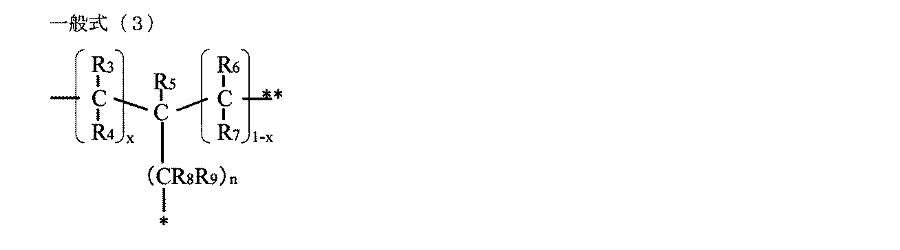
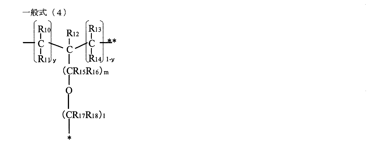
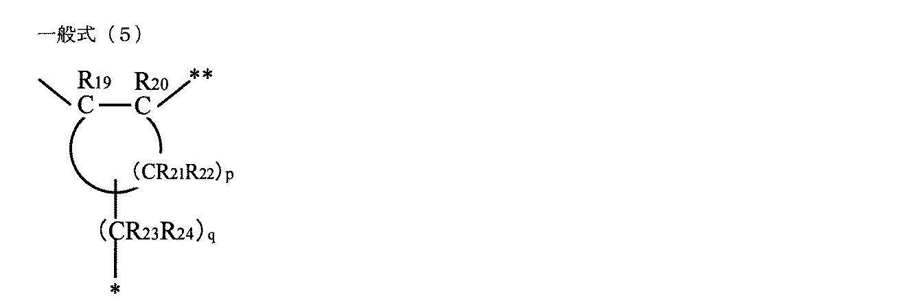
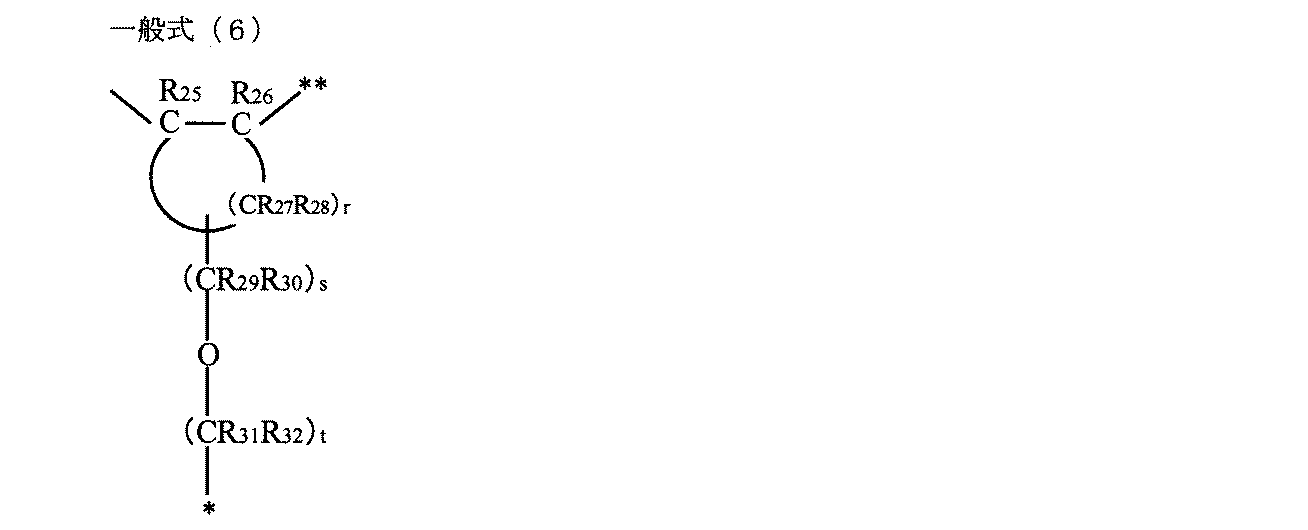
上記R3~R7、R10~R14、R19、R20、R25およびR26は、各々独立に水素原子、炭素数1~4のアルキル基、水酸基、カルボキシル基またはアミノ基を示す。R8、R9、R15~R18、R23、R24およびR29~R32は、各々独立に水素原子、または炭素数1~4のアルキル基を示す。R21、R22、R27およびR28は、各々独立に水素原子、炭素数1~4のアルコキシル基、または炭素数1~4のアルキル基を示す。n、m、l、q、sおよびtは、各々独立に1以上8以下の整数を示す。pおよびrは、各々独立に4以上12以下の整数を示す。xおよびyは、各々独立に0または1を示す。「*」および「**」は、各々、一般式(1)中のケイ素原子および酸素原子との結合部位を示す。
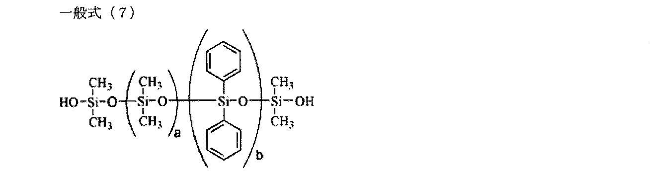


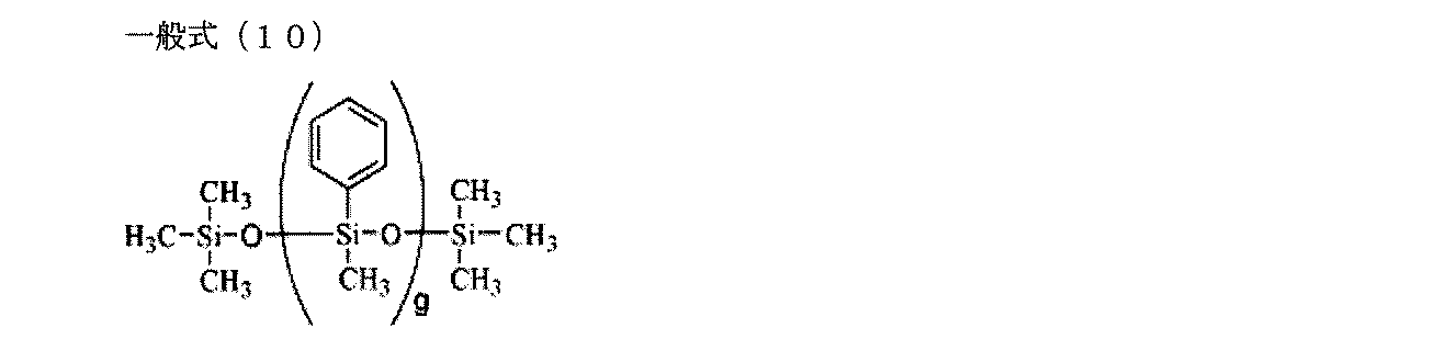
上記a~fは、各々独立に1以上の整数を示し、a+b、c+d、およびe+fは、各々独立に2以上670以下の整数を示す。gは、1以上20以下の整数を示す。
また、本発明の他の態様によれば、電子写真感光体と、該電子写真感光体に接触して配置されている上記の帯電部材とを有する電子写真装置が提供される。更に、本発明の他の態様によれば、電子写真感光体と、該電子写真感光体に接触して配置されている上記の帯電部材とを有し、電子写真装置の本体に着脱可能に構成されているプロセスカートリッジが提供される。
本発明によれば、トナーや外添剤の付着が抑制され、表面が汚れにくく、感光体との当接痕が電子写真画像に現れにくい帯電部材を得ることができる。また、本発明によれば、高品位な電子写真画像を安定して形成することのできるプロセスカートリッジおよび電子写真装置を得ることができる。
本発明に係る帯電部材は、支持体、該支持体上に形成された弾性層、および該弾性層上に形成された表面層を有する。
帯電部材の最も簡単な構成は、支持体上に弾性層および表面層の2層を設けた構成であるが、支持体と弾性層との間や弾性層と表面層との間に別の層を1つまたは2つ以上設けてもよい。帯電部材の代表例であるローラ形状の帯電ローラの断面を示した図1において、101は支持体であり、102は弾性層であり、103は表面層である。
帯電部材の最も簡単な構成は、支持体上に弾性層および表面層の2層を設けた構成であるが、支持体と弾性層との間や弾性層と表面層との間に別の層を1つまたは2つ以上設けてもよい。帯電部材の代表例であるローラ形状の帯電ローラの断面を示した図1において、101は支持体であり、102は弾性層であり、103は表面層である。
<支持体>
支持体としては導電性を有するものを用いることができる。具体例として以下のものが挙げられる。鉄、銅、ステンレス鋼、アルミニウム、アルミニウム合金又はニッケルで形成されている金属製(合金製)の支持体。
支持体としては導電性を有するものを用いることができる。具体例として以下のものが挙げられる。鉄、銅、ステンレス鋼、アルミニウム、アルミニウム合金又はニッケルで形成されている金属製(合金製)の支持体。
<弾性層>
弾性層には、従来の帯電部材の弾性層(導電性弾性層)に用いられているゴムなどの弾性体を1種または2種以上用いることができる。ゴムとしては以下のものが挙げられる。ウレタンゴム、シリコーンゴム、ブタジエンゴム、イソプレンゴム、クロロプレンゴム、スチレン-ブタジエンゴム、エチレン-プロピレンゴム、ポリノルボルネンゴム、スチレン-ブタジエン-スチレンゴム、アクリロニトリルゴム、エピクロルヒドリンゴムおよびアルキルエーテルゴム。
弾性層には、従来の帯電部材の弾性層(導電性弾性層)に用いられているゴムなどの弾性体を1種または2種以上用いることができる。ゴムとしては以下のものが挙げられる。ウレタンゴム、シリコーンゴム、ブタジエンゴム、イソプレンゴム、クロロプレンゴム、スチレン-ブタジエンゴム、エチレン-プロピレンゴム、ポリノルボルネンゴム、スチレン-ブタジエン-スチレンゴム、アクリロニトリルゴム、エピクロルヒドリンゴムおよびアルキルエーテルゴム。
また、弾性層には、導電剤を適宜使用することによって、その導電性を所定の値にすることができる。弾性層の電気抵抗値は、導電剤の種類および使用量を適宜選択することによって調整することができ、その電気抵抗値の好適な範囲は102~108Ωであり、より好適な範囲は103~106Ωである。また、弾性層用の導電剤として、ケッチェンブラックEC、アセチレンブラック、ゴム用カーボン、酸化処理を施したカラー(インク)用カーボン、および、熱分解カーボンなどの導電性のカーボンを用いることもできる。また、弾性層用の導電剤として、天然グラファイトおよび人造グラファイトの如きグラファイトを用いることもできる。弾性層には、無機または有機の充填剤や架橋剤を添加してもよい。
弾性層の硬度は、帯電部材と被帯電体である感光体とを当接させた際の帯電部材の変形を抑制する観点から、MD-1で60度以上85度以下、特には、70度以上80度以下であることが好ましい。
弾性層の表面粗さ(Rz)の目安としては、3.0μm以上12.0μm以下、特には、5.0以上10.0μm以下が好ましい。
弾性層は、上記の導電性弾性体の原料を密閉型ミキサー等で混合して、例えば、押出成形、射出成形、圧縮成形等の公知の方法により支持体上に形成される。尚、弾性層は必要に応じて接着剤を介して支持体上に接着される。支持体上に形成された弾性層は必要に応じて加硫処理される。加硫温度を急速に立ち上げると、加硫反応による加硫促進剤等の揮発性副生成物がガス化してボイドの要因となる。従って、加熱ゾーンを2つに分けて、第1ゾーンを加硫温度より低い状態に保持する事で、ガス成分を十分抜いた後に、第2ゾーンで加硫を行うことが好ましい。
<表面層>
本発明に係る帯電部材を構成する表面層は、特定の構成単位を有する高分子化合物と特定の構造を有するフェニル変性シリコーンオイルとを含む。
本発明に係る帯電部材を構成する表面層は、特定の構成単位を有する高分子化合物と特定の構造を有するフェニル変性シリコーンオイルとを含む。
〔高分子化合物〕
すなわち、本発明に係る高分子化合物は、下記一般式(1)で示される構成単位と、下記一般式(2)で示される構成単位と、Si-O-Tiの結合を有している。なお、高分子化合物がSi-O-Tiの結合を分子構造中に有することは、SiとTiが分子レベルで結合していることを示しており、このような高分子化合物を含む表面層は相分離のない均一な膜となりやすく、帯電部材として使用した際には帯電均一性をもつ表面層となる。高分子化合物が、一般式(1)で示される構成単位を有することにより、弾性層との密着性が向上する。高分子化合物が、一般式(2)で示される構成単位を有することにより、帯電能力の向上が期待できる。なお、TiO4/2とは、TiがOを介して他の原子(Si、Ti)との結合を4つ持つ状態にあることを意味する。
すなわち、本発明に係る高分子化合物は、下記一般式(1)で示される構成単位と、下記一般式(2)で示される構成単位と、Si-O-Tiの結合を有している。なお、高分子化合物がSi-O-Tiの結合を分子構造中に有することは、SiとTiが分子レベルで結合していることを示しており、このような高分子化合物を含む表面層は相分離のない均一な膜となりやすく、帯電部材として使用した際には帯電均一性をもつ表面層となる。高分子化合物が、一般式(1)で示される構成単位を有することにより、弾性層との密着性が向上する。高分子化合物が、一般式(2)で示される構成単位を有することにより、帯電能力の向上が期待できる。なお、TiO4/2とは、TiがOを介して他の原子(Si、Ti)との結合を4つ持つ状態にあることを意味する。


上記一般式(1)中、R1およびR2は、各々独立に以下の一般式(3)~(6)のいずれかを示す。

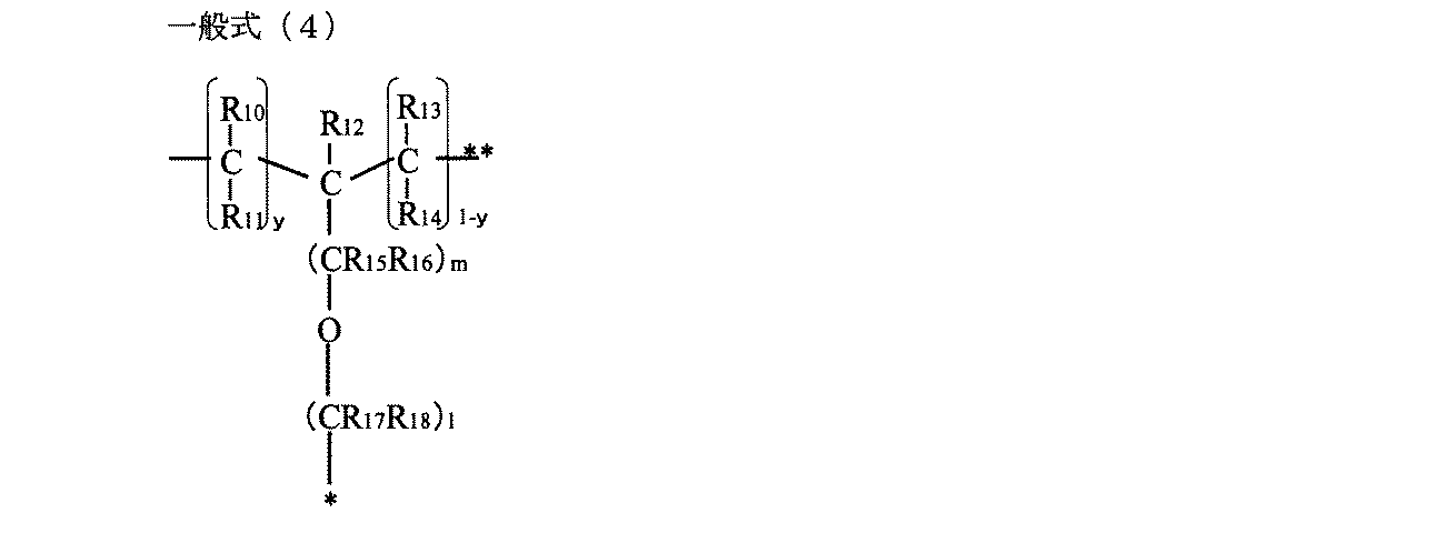

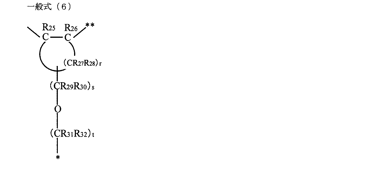
上記R3~R7、R10~R14、R19、R20、R25およびR26は、各々独立に水素原子、炭素数1以上4以下のアルキル基、水酸基、カルボキシル基またはアミノ基を示す。R8、R9、R15~R18、R23、R24およびR29~R32は、各々独立に水素原子、または炭素数1以上4以下のアルキル基を示す。R21、R22、R27およびR28は、各々独立に水素原子、炭素数1以上4以下のアルコキシル基、又は炭素数1以上4以下のアルキル基を示す。n、m、l、q、s、およびtは、各々独立に1以上8以下の整数を示す。pおよびrは、各々独立に4以上12以下の整数を示す。xおよびyは、各々独立に0または1を示す。「*」および「**」は、各々、一般式(1)のケイ素原子および酸素原子との結合部位を示す。
前記高分子化合物における一般式(1)のR1及びR2としては、各々独立に下記一般式(11)~(14)で示される構造から選ばれる何れかであることが好ましい。この場合、有機鎖が存在することで、表面層の弾性率の制御、あるいは表面層の膜特性としてのもろさや柔軟性の制御が可能となる。また有機鎖の構造、特にエーテル部位が存在すると、表面層の弾性層への密着性が向上する。
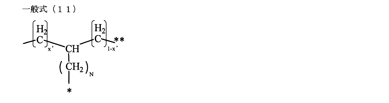
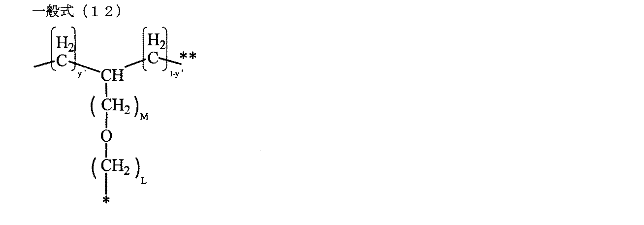
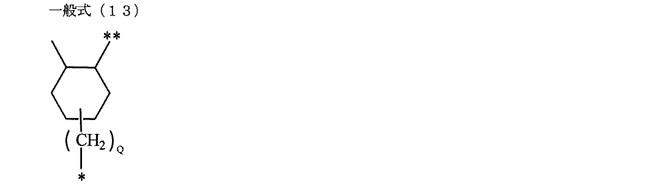

ここでN、M、L、Q、S及びTは、各々独立に1以上8以下の整数を示す。x’及びy’は、各々独立に0または1を示す。「*」および「**」は、各々、一般式(1)のケイ素原子及び酸素原子との結合部位を示す。
前記高分子化合物におけるチタンとケイ素との原子数比Ti/Siは0.1以上12.5以下であることが好ましい。帯電部材の帯電能力の向上の観点からこの値が0.1以上であれば好ましく、0.5以上であればより好ましい。また塗工性や混合液の保存性の向上の観点からこの値が12.5以下であれば好ましく、10.0以下であればより好ましい。
前記高分子化合物は、下記一般式(15)および(16)でそれぞれ示される加水分解性化合物の加水分解縮合物であることが好ましい。一般式(15)の3官能部位と、一般式(16)の4官能部位とで生じる加水分解と縮合の程度を制御することで、表面層の弾性率、緻密性を制御することができる。
また、一般式(15)のR33の有機鎖部位を硬化サイトとして用いることで、表面層の強靭さ、および表面層の弾性層への密着性の制御が可能である。また、R33を紫外線照射により開環するエポキシ基を有する有機基とすることで、従来の熱硬化性材料と比較して硬化時間を短縮でき、弾性層の熱劣化を抑制することができる。
また、一般式(15)のR33の有機鎖部位を硬化サイトとして用いることで、表面層の強靭さ、および表面層の弾性層への密着性の制御が可能である。また、R33を紫外線照射により開環するエポキシ基を有する有機基とすることで、従来の熱硬化性材料と比較して硬化時間を短縮でき、弾性層の熱劣化を抑制することができる。

上記一般式(15)中、R33は、エポキシ基を有する下記一般式(17)~(20)のいずれかを示し、R34~R36は、各々独立に炭素数1~4のアルキル基を示す。また一般式(16)中、R37~R40は、各々独立に炭素数1~9のアルキル基を示す。



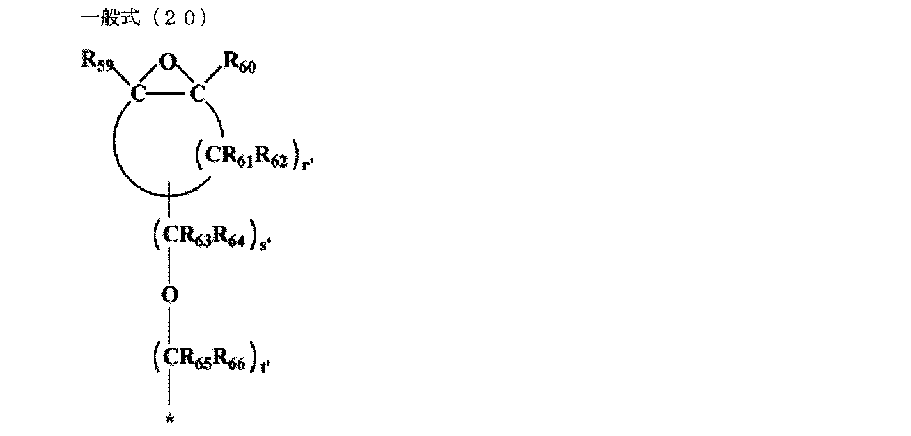
上記一般式(17)~(20)中、R41~R43、R46~R48、R53、R54、R59およびR60は、各々独立に水素原子、炭素数1~4のアルキル基、水酸基、カルボキシル基、またはアミノ基を示す。R44、R45、R49~R52、R57、R58およびR63~R66は、各々独立に水素原子または炭素数1~4のアルキル基を示す。R55、R56、R61およびR62は、各々独立に水素、炭素数1~4のアルコキシル基または炭素数1~4のアルキル基を示す。n’、m’、l’、q’、s’およびt’は、各々独立に1~8の整数を示す。p’およびr’は、各々独立に4以上12以下の整数を示す。また、「*」は、一般式(15)のケイ素原子との結合部位を示す。
上記一般式(15)中のR34~R36の炭化水素基としては、例えば、アルキル基、アルケニル基およびアリール基などが挙げられる。これらの中でも、炭素数1~4の直鎖状もしくは分岐鎖状のアルキル基が好ましく、更にはメチル基、エチル基、n-プロピル基、i-プロピル基、n-ブチル基、t-ブチル基がより好ましい。
以下に、上記一般式(15)で示される構造を有する加水分解性シラン化合物の具体例を示す。4-(1,2-エポキシブチル)トリメトキシシラン、5,6-エポキシヘキシルトリエトキシシラン、8-オキシラン-2-イルオクチルトリメトキシシラン、8-オキシラン-2-イルオクチルトリエトキシシラン、3-グリシドキシプロピルトリメトキシシラン、3-グリシドキシプロピルトリエトキシシラン、1-(3,4-エポキシシクロヘキシル)エチルトリメトキシシラン、1-(3,4-エポキシシクロヘキシル)エチルトリエトキシシラン、3-(3,4-エポキシシクロヘキシル)メチルオキシプロピルトリメトキシシラン、3-(3,4-エポキシシクロヘキシル)メチルオキシプロピルトリエトキシシラン。
上記一般式(16)中のR37~R40の炭化水素基としては、反応速度の観点からいずれも炭素数1以上18以下の炭化水素基であることが好ましい。
以下に、上記一般式(16)で示される構造を有する加水分解性チタン化合物の具体例を示す。チタニウムメトキシド、チタニウムエトキシド、チタニウムn-プロポキシド、チタニウムi-プロポキシド、チタニウムn-ブトキシド、チタニウムt-ブトキシド、チタニウムi-ブトキシド、チタニウムノニルオキシド、チタニウム2-エチルヘキソキシド、チタニウムメトキシプロポキシド。
以下に、上記一般式(17)で示される構造を有する加水分解性シラン化合物の具体例を示す。4-(1,2-エポキシブチル)トリメトキシシラン、4-(1,2-エポキシブチル)トリエトキシシラン、5,6-エポキシヘキシルトリメトキシラン、5,6-エポキシヘキシルトリエトキシラン、8-オキシラン-2-イルオクチルトリメトキシシラン、8-オキシラン-2-イルオクチルトリエトキシシラン。
以下に、上記一般式(18)で示される構造を有する加水分解性シラン化合物の具体例を示す。グリシドキシプロピルトリメトキシシラン、グリシドキシプロピルトリエトキシシラン。
以下に、上記一般式(19)で示される構造を有する加水分解性シラン化合物の具体例を示す。2-(3,4-エポキシシクロヘキシル)エチルトリメトキシシラン、2-(3,4-エポキシシクロヘキシル)エチルトリエトキシシラン。
以下に、上記一般式(20)で示される構造を有する加水分解性シラン化合物の具体例を示す。3-(3,4-エポキシシクロヘキシル)メチルオキシプロピルトリメトキシシラン、3-(3,4-エポキシシクロヘキシル)メチルオキシプロピルトリエトキシシラン。
更に本発明における前記高分子化合物は、上記一般式(15)及び(16)で示される加水分解性化合物と、下記一般式(21)で示される加水分解性化合物との架橋物であることが好ましい。この場合、合成段階での一般式(15)及び(16)の化合物の溶解性、塗工性、更に硬化後の膜物性として、電気特性を向上させることが可能となる。特にR67がアルキル基の場合、溶解性、塗工性が改善されるので、好ましい。また、R67がフェニル基の場合は、電気特性、特に体積抵抗率の向上に寄与するので、好ましい。

上記一般式(21)中、R67は、アルキル基またはフェニル基を示し、アルキル基としては、炭素数1~21の直鎖状のアルキル基が好ましく、更には炭素数6~10のものが好ましい。R68~R70は、各々独立に炭素数1~4のアルキル基を示す。
以下に、上記一般式(21)で示される構造を有する加水分解性シラン化合物の具体例を示す。メチルトリメトキシシラン、メチルトリエトキシシラン、メチルトリプロポキシシラン、エチルトリメトキシシラン、エチルトリエトキシシラン、エチルトリプロポキシシラン、プロピルトリメトキシシラン、プロピルトリエトキシシラン、プロピルトリプロポキシシラン、ヘキシルトリメトキシシラン、ヘキシルトリエトキシシラン、ヘキシルトリプロポキシシラン、デシルトリメトキシシラン、デシルトリエトキシシラン、デシルトリプロポキシシラン、フェニルトリメトキシシラン、フェニルトリエトキシシラン、フェニルトリプロポキシシラン。
上記一般式(21)で示される構造を有する加水分解性シラン化合物を併用する場合、R67が炭素数6~10の直鎖状のアルキル基を有する加水分解性シラン化合物と、R67がフェニル基を有する加水分解性シラン化合物を組み合わせることが好ましい。この場合は、加水分解・縮合反応によりモノマー構造が変化しても溶媒への相溶性が良好である。
〔フェニル変性シリコーンオイル〕
本発明に係る表面層は、上記した高分子化合物と共に、下記一般式(7)~(10)で示される構造を有するフェニル変性シリコーンオイルからなる群から選択される少なくとも1つのフェニル変性シリコーンオイル(以下、単に「シリコーンオイル」という場合がある。)を含有している。
本発明に係る表面層は、上記した高分子化合物と共に、下記一般式(7)~(10)で示される構造を有するフェニル変性シリコーンオイルからなる群から選択される少なくとも1つのフェニル変性シリコーンオイル(以下、単に「シリコーンオイル」という場合がある。)を含有している。
そして、これらのシリコーンオイルは、帯電部材の表面層中に含有させた場合においても、当該帯電部材の帯電能力に大きな変化を与えることがない。そのため、帯電部材の一部に、感光体との長期間に亘る当接によって圧縮永久歪みが生じ、シリコーンオイルが圧縮永久歪みの発生部分の周囲に偏って存在した場合にも、圧縮永久歪みの発生部分とそれ以外の部分とにおける帯電能力に差が生じにくい。

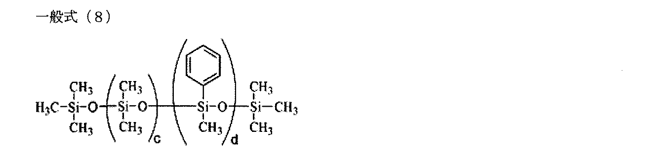
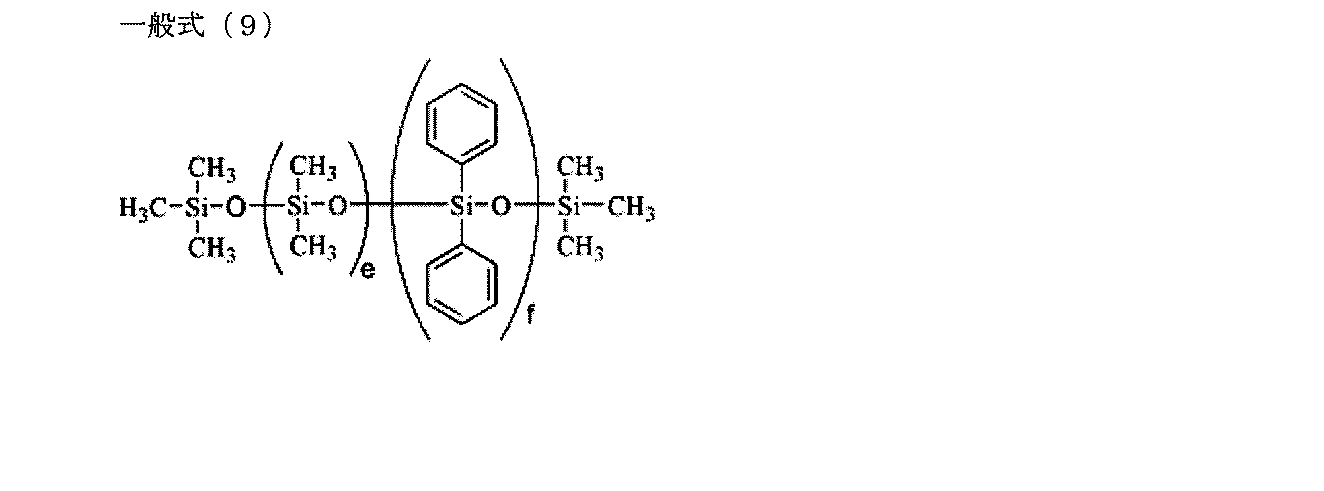
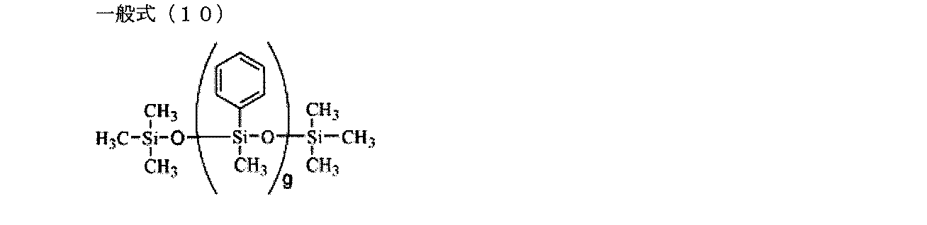
上記一般式(7)~(10)中、a~fは、各々独立に1以上の整数を示し、a+b、c+d、およびe+fは、各々独立に2以上670以下の整数を示す。gは、1以上20以下の整数を示す。
フェニル変性シリコーンオイルは、フェニル基を含む有機鎖の結合位置により、ジフェニル-ジメチル型、フェニルメチル-ジメチル型、フェニル-メチル型、の3種類に分類でき、さらに末端が変性型と未変性型とに分類できる。中でもトナーやトナー外添剤などの付着抑制の観点からジメチル含有のものが好ましく、さらに感光体の表面電位の上昇の抑制効果を発揮しやすいジフェニル含有のものが好ましい。なお、上記一般式(7)で示されるシリコーンオイルは、末端シラノール変性ジフェニル-ジメチル型である。上記一般式(8)で示されるシリコーンオイルは末端未変性フェニルメチル-ジメチル型である。上記一般式(9)で示されるシリコーンオイルは末端未変性ジフェニル-ジメチル型である。また、上記一般式(10)で示されるシリコーンオイルは末端未変性フェニル-メチル型である。
以下に、上記一般式(7)で示される構造を有するフェニル変性シリコーンオイルの具体例を示す。PDS-1615(商品名、粘度50~60、Gelest社製)、およびPDS-0338(商品名、粘度6000~8000、Gelest社製)。
以下に、上記一般式(8)で示される構造を有するフェニル変性シリコーンオイルの具体例を示す。SH510-100CS(商品名、粘度100、東レ・ダウコーニング(株)製)、およびSH510-500CS(商品名、粘度500、東レ・ダウコーニング(株)製)。
以下に、上記一般式(9)で示される構造を有するフェニル変性シリコーンオイルの具体例を示す。KF50-100CS(商品名、粘度100、信越化学工業(株)製)、およびKF50-1000CS(商品名、粘度1000、信越化学工業(株)製)。
以下に、上記一般式(10)で示される構造を有するフェニル変性シリコーンオイルの具体例を示す。PMM-0011(商品名、粘度10~20、Gelest社製)、およびPMM-0025(商品名、粘度500、Gelest社製)。
シリコーンオイルの質量平均分子量Mwは、100以上50000以下が好ましい。100以上であれば、表面自由エネルギーを低下させる効果が大きくなり好ましく、50000以下であれば、表層用塗布液との親和性が大きくなり、塗工ムラの原因となる白濁が起こりにくいため好ましい。質量平均分子量は、より好ましくは、300以上である。
なお、シリコーンオイルの質量平均分子量の測定には、GPC装置としてHLC-8120GPC(商品名、東ソー(株)製)を用いることができる。カラムは、「商品名:TSK guardcolum SuperH-L」、「商品名:TSKgel SuperH4000」、「商品名:TSKgel SuperH3000」、「商品名:TSKgel SuperH2000」、および「商品名:TSKgel SuperH1000」を5本連結して用いることができる。溶離液として、高速液体クロマトグラフィー用トルエンを用いることができ、温度は、INLET:40℃、OVEN:40℃、RI:40℃とすることができる。検出器はRIで行うことができ、検量線はポリスチレン(EasiCal PS-2)を用いることができる。
帯電部材の表面自由エネルギーは30mJ/m2以下が好ましい。30mJ/m2以下であればトナーや外添剤等の付着物との親和性が低いため、表面付近に付着物が存在しても固着しにくくなる。表面自由エネルギーは、接触角計CA-X RALL型、協和界面(株)製を用いて測定することができる。また、表面自由エネルギーの解析には北崎・畑理論を用いることができ、表面自由エネルギー(γtotal)は以下の式より算出される。
γtotal=γd+γp+γh
上式において、γdは分散項、γpは極性項、γhは水素結合項の成分を表し、γtotalは各成分の和を示す。
γtotal=γd+γp+γh
上式において、γdは分散項、γpは極性項、γhは水素結合項の成分を表し、γtotalは各成分の和を示す。
帯電部材の表面層の動摩擦係数は対ポリエチレンテレフタレート(PET)シートでの測定において0.1以上0.4以下が好ましい。0.1以上であれば感光体との従動が良好でスリップを容易に防止することができ、感光体へ安定して帯電付与することが容易にできる。また0.4以下であればトナーなどの付着が特に少なく、帯電不良を起こすことを容易に防ぐことができる。
図4に動摩擦係数の測定装置を示す。図4において、測定対象である帯電部材201は、ベルト202に所定の角度θで接触している。ベルト202の一端には重り203が繋がれ、他端には荷重計204が繋がれている。また荷重計204には記録計205が接続されている。なお、後述する実施例では、ベルトとして、厚さ100μ、幅30mm、長さ180mm、PET製(商品名:ルミラーS10 #100、東レ(株)製)のものが用いられている。
図4に示す状態で、帯電部材201を所定の方向および所定の速度で回転させたとき、荷重計204で測定された力をF[N]、重りの重さとベルトの重さとの和をW[N]とすると、摩擦係数は以下の式で求められる。なお、この測定方法は、オイラーのベルト式に準拠している。
摩擦係数=(1/θ)ln(F/W)
後述する実施例では、Wを0.98[N](100g重)とし、帯電部材の回転速度を115rpmとし、測定環境を23℃、相対湿度を50%として、測定されている。
摩擦係数=(1/θ)ln(F/W)
後述する実施例では、Wを0.98[N](100g重)とし、帯電部材の回転速度を115rpmとし、測定環境を23℃、相対湿度を50%として、測定されている。
また、架橋反応の際、架橋効率の向上の観点から、光重合開始剤であるカチオン重合触媒を共存させておくことが好ましい。例えば、活性エネルギー線によって賦活化されるルイス酸のオニウム塩に対してエポキシ基は高い反応性を示すことから、上記のカチオン重合可能な基がエポキシ基である場合、カチオン重合触媒としては、ルイス酸のオニウム塩を用いることが好ましい。
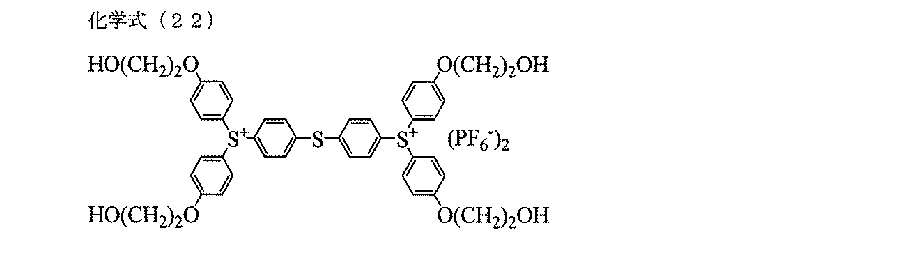
その他のカチオン重合触媒としては、例えば、ボレート塩、イミド構造を有する化合物、トリアジン構造を有する化合物、アゾ化合物、過酸化物が挙げられる。各種カチオン重合触媒の中でも、感度、安定性および反応性の観点から、芳香族スルホニウム塩や芳香族ヨードニウム塩が好ましい。特には、ビス(4-tert-ブチルフェニル)ヨードニウム塩や、下記化学式(22)で示される構造を有する化合物(商品名:アデカオプトマ-SP150、アデカ(株)製)や、下記化学式(23)で示される構造を有する化合物(商品名:イルガキュア261、チバスペシャルティーケミカルズ社製)が好ましい。

また、光重合開始剤であるカチオン重合触媒の添加量は、加水分解縮合物100質量部に対して、1.0~3.0質量部であることが好ましい。この範囲内であれば硬化特性、および光重合開始剤の溶解性が良好となる。
本発明に係る帯電部材は、上記の加水分解縮合物およびフェニル変性シリコーンオイルを含む塗料の塗膜を弾性層の外周に形成した後に、該塗膜中の加水分解縮合物を架橋させて上記高分子化合物を形成することによって得られる。
<帯電部材の製造方法>
以下に、本発明の帯電部材の製造方法を例示する。「製法例1」は、上記一般式(15)および(16)の化合物、並びに上記一般式(7)~(10)で示されるフェニル変性シリコーンオイルのうちのいずれかを用いて製造する方法である。また「製法例2」は、上記一般式(15)(16)及び(21)の化合物、並びに上記一般式(7)~(10)で示されるフェニル変性シリコーンオイルのうちのいずれかを用いて製造する方法である。
以下に、本発明の帯電部材の製造方法を例示する。「製法例1」は、上記一般式(15)および(16)の化合物、並びに上記一般式(7)~(10)で示されるフェニル変性シリコーンオイルのうちのいずれかを用いて製造する方法である。また「製法例2」は、上記一般式(15)(16)及び(21)の化合物、並びに上記一般式(7)~(10)で示されるフェニル変性シリコーンオイルのうちのいずれかを用いて製造する方法である。
前記製法例1においては、以下の第1の工程(i)および第2の工程(ii)が含まれる。
(i)前記一般式(15)で示される構造を有する加水分解性化合物と、前記一般式(16)で示される構造を有する加水分解性化合物との加水分解縮合物及び前記一般式(7)~(10)で示されるフェニル変性シリコーンオイルの群から選択される1つまたは複数のフェニル変性シリコーンオイルを含む表面層形成用塗料の塗膜を、支持体の外周に配置された弾性層の上に形成する第1の工程。
(ii)該塗膜中の該加水分解縮合物のR33のエポキシ基を開裂させることにより該加水分解縮合物を架橋させて前記高分子化合物を製造する第2の工程。
(i)前記一般式(15)で示される構造を有する加水分解性化合物と、前記一般式(16)で示される構造を有する加水分解性化合物との加水分解縮合物及び前記一般式(7)~(10)で示されるフェニル変性シリコーンオイルの群から選択される1つまたは複数のフェニル変性シリコーンオイルを含む表面層形成用塗料の塗膜を、支持体の外周に配置された弾性層の上に形成する第1の工程。
(ii)該塗膜中の該加水分解縮合物のR33のエポキシ基を開裂させることにより該加水分解縮合物を架橋させて前記高分子化合物を製造する第2の工程。
前記製法例2の場合は、前記工程(i)において一般式(15)の加水分解性化合物の代わりに、前記一般式(15)と(21)の加水分解性化合物の混合物が使用される。
工程(i)においては、加水分解性シラン化合物に水とアルコールを添加し、加熱還流により加水分解・縮合を行う工程(iii)(第1段階反応)が行われる。更にこの工程(iii)で得られた加水分解・縮合した溶液に対して前記一般式(16)で示される構造を有する加水分解性化合物を添加して加水分解・縮合を行う工程(iv)(第2段階反応)が行われる。
次に、工程(iv)で得られた溶液に、一般式(7)~(10)で示されるフェニル変性シリコーンオイルから成る群から選択される1つまたは2つ以上のフェニル変性シリコーンオイル、及び前記光重合開始剤を添加する工程(v)を経て、工程(ii)を行うのが好ましい。
工程(iii)及び(iv)の2段階の合成反応を経るのは、一般式(15)の加水分解性化合物、あるいは一般式(15)と一般式(21)の加水分解性化合物との組み合わせによる反応速度と、一般式(16)の加水分解性化合物の反応速度が非常に異なるため、つまり一般式(16)の化合物の反応速度が非常に速いためである。Ti/Si比が0.10~0.30程度(Tiの濃度が小さい領域)であれば、加水分解・縮合反応を2段階に分割しなくても反応は円滑に進行する。しかし、Ti/Si比が0.30~12.50(Tiの濃度が大きい領域)では、前述した反応速度の差により一般式(16)の加水分解性化合物のみが選択的に反応し、白濁・沈殿が生じ易くなる。
また、加水分解縮合物を合成する際の加水分解性シラン化合物に対する水の添加量の割合WR(モル比)が0.3以上6.0以下であることが好ましい。
WR=水/{加水分解性化合物(15)+加水分解性化合物(21)}
WRの値は1.2以上3.0以下が好ましい。水の添加量が上記範囲内であれば、合成時の縮合の程度を制御し易くなる。また縮合速度の制御もし易く、加水分解縮合物とフェニル変性シリコーンオイルとの混合液や表面層形成用塗布液のライフの安定性にも効果がある。また上記範囲内であれば、前記一般式(15)のエポキシ基が開環しないpH領域で合成が行えるので好ましい。
WR=水/{加水分解性化合物(15)+加水分解性化合物(21)}
WRの値は1.2以上3.0以下が好ましい。水の添加量が上記範囲内であれば、合成時の縮合の程度を制御し易くなる。また縮合速度の制御もし易く、加水分解縮合物とフェニル変性シリコーンオイルとの混合液や表面層形成用塗布液のライフの安定性にも効果がある。また上記範囲内であれば、前記一般式(15)のエポキシ基が開環しないpH領域で合成が行えるので好ましい。
また、加水分解縮合物を合成する際のアルコールとして、第1級アルコールのみ、第1級アルコールと第2級アルコールの混合系、または第1級アルコールと第3級アルコールの混合系を用いることが好ましい。特にエタノールのみ、メタノール/2-ブタノールの混合系、エタノール/2-ブタノールの混合系が好ましい。
フェニル変性シリコーンオイルの使用量は、一般式(15)と一般式(16)の加水分解性化合物の加水分解縮合物、あるいは一般式(15)と一般式(21)の加水分解性化合物との組み合わせと一般式(16)の加水分解性化合物との加水分解縮合物100質量部に対して、1.0質量部以上30質量部以下であることが好ましい。1.0質量部以上であれば表面自由エネルギーが容易に低下し、付着物の親和性の調整に効果的であることから好ましく、30質量部以下であれば帯電特性の維持の観点から好ましい。
また光重合開始剤は混合液との相溶性を向上させるために事前にアルコールやケトンなどの溶媒に希釈することができる。希釈に用いる溶媒としては、例えばメタノール、アセトン、メチルエチルケトン(MEK)、メチルイソブチルケトン(MIBK)が挙げられる。
次に、得られた加水分解縮合物とフェニル変性シリコーンオイルとを含む混合液を適正な濃度に調整して表面層形成用塗料とする。これを、支持体および該支持体上に形成された弾性層を有する部材上に塗布する。
表面層形成用塗料を調製する際には、塗布性向上のために、加水分解縮合物の合成に使用した溶剤以外に、揮発性を考慮した適当な溶剤を用いても良い。適当な溶剤としては、2-ブタノール、酢酸エチル、メチルエチルケトン、あるいは、これらを混合したものが挙げられる。表面層形成用塗布液の濃度は、表面自由エネルギーを低下させる観点、および感光体の表面電位の上昇を抑制する観点から、0.05質量%以上とすることが好ましく、塗工ムラを抑える観点から、4.0質量%以下とすることが好ましい。
また、表面層形成用塗布液を弾性層上に塗布する際には、ロールコーターを用いた塗布、浸漬塗布、リング塗布などを採用することができる。
次に、弾性層上に形成されてなる表面層形成用塗布液の塗膜に対して活性エネルギー線を照射し、当該塗膜中の加水分解縮合物が有するカチオン重合可能な基を開裂させる。これによって該塗膜中の加水分解縮合物を架橋させ、表面層を形成する。活性エネルギー線としては、紫外線が好ましい。表面層の硬化を紫外線で行うことで、余分な熱が発生しにくく、熱硬化のような溶剤の揮発中における相分離が生じにくく、均一な膜状態が得られる。このため、感光体への均一で安定した電位を与えることができる。また、架橋反応を紫外線によって行えば、熱履歴による弾性層の劣化を抑制することができるため、弾性層の電気的特性の低下を抑制することもできる。
紫外線の照射には、高圧水銀ランプ、メタルハライドランプ、低圧水銀ランプ、又はエキシマUVランプなどを用いることができ、これらのうち、紫外線の波長が150~480nmの光を豊富に含む紫外線源が用いられる。なお、紫外線の積算光量は、以下のように定義される。
紫外線積算光量[mJ/cm2]=紫外線強度[mW/cm2]×照射時間[s]
紫外線の積算光量の調節は、照射時間や、ランプ出力や、ランプと被照射体との距離で行うことが可能である。また、照射時間内で積算光量に勾配をつけてもよい。
紫外線積算光量[mJ/cm2]=紫外線強度[mW/cm2]×照射時間[s]
紫外線の積算光量の調節は、照射時間や、ランプ出力や、ランプと被照射体との距離で行うことが可能である。また、照射時間内で積算光量に勾配をつけてもよい。
低圧水銀ランプを用いる場合、紫外線の積算光量は、ウシオ電機(株)製の紫外線積算光量計「UIT-150-A」や「UVD-S254」を用いて測定することができる。エキシマUVランプを用いる場合、紫外線の積算光量は、ウシオ電機(株)製の紫外線積算光量計「UIT-150-A」や「VUV-S172」を用いて測定することができる。
架橋および硬化反応の具体例を図7に示す。すなわち、上記一般式(15)で示される化合物として3-グリシドキシプロピルトリメトキシシランを用いると共に、上記一般式(21)および(16)で示される化合物を加水分解させて生成する縮合物は、カチオン重合可能な基としてエポキシ基(グリシドキシプロピル基)を有する。このような加水分解縮合物のエポキシ基はカチオン重合触媒(図7中、R+X-と記載)の存在下で、エポキシ環が開環し、連鎖的に重合が進む。その結果、TiO4/2およびSiO3/2を含むポリシロキサン同士が架橋し、硬化して本発明に係る表面層が形成される。なお図7中、nは1以上の整数を示す。
表面層の膜厚の目安としては、帯電能力、弾性層を有する場合における弾性層からの低分子成分のブリードアウトの抑制等の観点から、10~400nm、特には、50~350nmが好ましい。
<電子写真装置及びプロセスカートリッジ>
図2に、本発明の帯電部材を有するプロセスカートリッジを備えた電子写真装置の概略構成の一例を示す。この電子写真装置は、軸2を中心に矢印方向に所定の周速度で回転駆動される円筒状の感光体1を有する。感光体は支持体、支持体上に形成された感光層、電荷注入層、表面層等を有するものであってもよい。
図2に、本発明の帯電部材を有するプロセスカートリッジを備えた電子写真装置の概略構成の一例を示す。この電子写真装置は、軸2を中心に矢印方向に所定の周速度で回転駆動される円筒状の感光体1を有する。感光体は支持体、支持体上に形成された感光層、電荷注入層、表面層等を有するものであってもよい。
回転駆動される感光体の表面は、帯電部材3により、正又は負の所定電位に均一に帯電され、次いで、スリット露光やレーザービーム走査露光の露光手段(不図示)から出力される露光光(画像露光光)4を受け、目的の画像に対応した静電潜像が形成される。
帯電部材3による感光体1の表面の帯電の際、帯電部材3には、電圧印加手段(不図示)から直流電圧或いは直流電圧に交流電圧を重畳した電圧が印加される。
感光体1の表面に形成された静電潜像は、現像手段5に設けられる現像ローラにより現像剤が供給され反転現像又は正規現像されてトナー像となる。次いで、感光体1の表面のトナー像は、転写ローラ6に印加される転写バイアスによって、感光体1と転写ローラ6との間に感光体の回転と同期して搬送された紙等の転写材Pに順次転写される。
現像手段としては、例えば、ジャンピング現像手段、接触現像手段、磁気ブラシ手段等が挙げられる。また、転写ローラとしては、支持体上に中抵抗に調整された弾性層を有するものを使用することができる。
トナー像が転写された転写材Pは、感光体1の表面から分離されて定着手段8へ導入されて、トナー像が定着された画像形成物(プリント、コピー)として装置外へプリントアウトされる。両面画像形成モードや多重画像形成モードの場合、この画像形成物は、再循環搬送機構に導入されて転写部へ再導入される。
トナー像転写後の感光体1の表面は、クリーニングブレード等のクリーニング手段7によって転写残りの現像剤(トナー)が除去され清浄面化され、さらに前露光手段からの前露光光により除電処理された後、繰り返し画像形成に使用される。帯電手段が接触帯電手段である場合は、前露光は必ずしも必要ではない。
このプロセスカートリッジ9は、感光体1、帯電部材3、現像手段5、クリーニング手段7が一体化された構成であって、電子写真装置本体のレール等の案内手段10を用いて電子写真装置の本体に着脱可能な構造とされている。上記部材の他、転写手段等から適宜選択してカートリッジ化し、電子写真装置の本体に着脱可能とすることもできる。
更に図3に上記現像手段5の現像装置の模式断面図を示す。図3において、公知のプロセスにより形成された静電潜像を保持する保持体としての電子写真感光体ドラム501は、矢印B方向に回転される。現像剤担持体としての現像スリーブ508は、現像剤容器としてのホッパ503によって供給された磁性トナーを有する一成分系現像剤504を担持して、矢印A方向に回転する。こうすることによって、現像スリーブ508と感光体ドラム501とが対向している現像領域Dに現像剤504を搬送する。図3に示すように、現像スリーブ508内には、現像剤504を現像スリーブ508上に磁気的に吸引且つ保持するために、磁石が内接されているマグネットローラ505が配置されている。
本発明の現像装置で用いられる現像スリーブ508は、支持体としての金属円筒管506と、その上に被覆された導電性樹脂被覆層507を有する。ホッパ503中には、現像剤504を攪拌するための攪拌翼510が設けられている。513は、現像スリーブ508とマグネットローラ505とが非接触状態にあることを示す間隙である。現像剤504は、現像剤を構成する磁性トナー相互間及び現像スリーブ508上の導電性樹脂被覆層507との摩擦により、感光体ドラム501上の静電潜像を現像することが可能な摩擦帯電電荷を得る。図3の例では、現像領域Dに搬送される現像剤504の層厚を規制するために、現像剤層厚規制部材としての強磁性金属製の磁性規制ブレード511が設けられている。この磁性規制ブレード511は、現像スリーブ508の表面から約50~500μmのギャップ幅を持って現像スリーブ508に臨むように、ホッパ503から垂下されている。マグネットローラ505の磁極N1からの磁力線が磁性規制ブレード511に集中することにより、現像スリーブ508上に現像剤504の薄層が形成される。
また、本発明で使用する現像剤(トナー)は、いずれの形式であっても、質量平均粒径が4μm以上11μm以下の範囲にあることが好ましい。このようなものを使用すれば、トナーの帯電量あるいは画質及び画像濃度等がバランスのとれたものとなる。現像剤(トナー)用結着樹脂としては、一般に公知の樹脂が使用可能であり、例えばビニル系樹脂、ポリエステル樹脂、ポリウレタン樹脂、エポキシ樹脂、フェノール樹脂等が挙げられるが、この中でもビニル系樹脂、ポリエステル樹脂が好ましい。
現像剤(トナー)には帯電特性を向上させる目的で、荷電制御剤をトナー粒子に包含させること(内添)、又はトナー粒子と混合して用いること(外添)ができる。これは、荷電制御剤によって、現像システムに応じた最適の荷電量コントロールが可能となるためである。
正の荷電制御剤としては、例えば以下のものが挙げられる。ニグロシン、トリアミノトリフェニルメタン系染料及び脂肪酸金属塩等による変性物;トリブチルベンジルアンモニウム-1-ヒドロキシ-4-ナフトスルホン酸塩、テトラブチルアンモニウムテトラフルオロボレートなどの四級アンモニウム塩;ジブチルスズオキサイド、ジオクチルスズオキサイド、ジシクロヘキシルスズオキサイドなどのジオルガノスズオキサイド;ジブチルスズボレート、ジオクチルスズボレード、ジシクロヘキシルスズボレートなどのジオルガノスズボレート。これらは単独であるいは2種類以上を組み合わせて用いることができる。
また、負の荷電制御剤としては、例えば、有機金属化合物、キレート化合物が有効である。その例としては、アルミニウムアセチルアセトナート、鉄(II)アセチルアセトナート、3,5-ジターシャリーブチルサリチル酸クロム等があり、特にアセチルアセトン金属錯体、モノアゾ金属錯体、ナフトエ酸あるいはサリチル酸系の金属錯体又は塩が好ましい。
現像剤(トナー)が、磁性現像剤(トナー)である場合、磁性材料として、例えば以下のものが挙げられる。マグネタイト、マグヘマイト、フェライト等の酸化鉄系金属酸化物;Fe、Co、Ni等の磁性金属;これらの金属とAl、Cu、Pb、Mg、Ni、Sn、Zn、Sb、Be、Bi、Cd、Ca、Mn、Se、Ti、W、V等の金属との合金;及びこれらの混合物等。その際は、これら磁性材料に着色剤としての役目を兼用させても構わない。
現像剤(トナー)に配合する着色剤として、従来からこの分野で使用している顔料、染料を使用することが可能であり、適宜選択して使用すればよい。現像剤(トナー)には離型剤を配合することが好ましく、例えば以下のものが挙げられる。低分子量ポリエチレン、低分子量ポリプロピレン、マイクロクリスタリンワックス、パラフィンワックスなどの脂肪族炭化水素系ワックス、カルナウバワックス、フィッシャートロプシュワックス、サゾールワックス、モンタンワックス等の脂肪酸エステルを主成分とするワックス類等。
さらに、現像剤(トナー)には、環境安定性、帯電安定性、現像性、流動性、保存性向上及びクリーニング性向上のために、シリカ、酸化チタン、アルミナ等の無機微粉体を外添すること、すなわち現像剤の表面近傍に存在させていることが好ましい。中でも、シリカ微粉体が好ましい。
以下に、具体的な実施例を挙げて本発明をさらに詳細に説明する。先ず、実施例に先立って、導電性弾性ローラの作製及び評価ついて説明する。なお、実施例中の「部」は「質量部」を意味する。
〔1〕導電性弾性ローラ1の作製及び評価
表1に示す材料を6L加圧ニーダー(使用装置:TD6-15MDX、トーシン社製)で20分間混練し、次いで加硫促進剤としてのテトラベンジルチウラムジスルフィド[商品名:サンセラーTBzTD、三新化学工業(株)製]4.5部、加硫剤としての硫黄1.2部を加え、ロール径12インチのオープンロールでさらに8分間混練することによって未加硫ゴム組成物を得た。
表1に示す材料を6L加圧ニーダー(使用装置:TD6-15MDX、トーシン社製)で20分間混練し、次いで加硫促進剤としてのテトラベンジルチウラムジスルフィド[商品名:サンセラーTBzTD、三新化学工業(株)製]4.5部、加硫剤としての硫黄1.2部を加え、ロール径12インチのオープンロールでさらに8分間混練することによって未加硫ゴム組成物を得た。

次に、直径6mm、長さ252mmの円柱形の鋼製の支持体(表面をニッケルメッキ加工したもの)の円柱面軸方向中央を挟んで両側115.5mmまでの領域(あわせて軸方向幅231mmの領域)に、金属およびゴムを含む熱硬化性接着剤(商品名:メタロックN-33、(株)東洋化学研究所製)を塗布し、これを30分間、温度80℃で乾燥させた後、さらに1時間、温度120℃で乾燥させた。
次にクロスヘッド押出機を使用して、上記接着層付き支持体上に未加硫ゴム組成物を同軸状に外径8.75~8.90mmの円筒形に押出し、端部を切断して、支持体の外周に未加硫ゴム組成物の層(長さ242mm)を形成した。押出機はシリンダー径70mm、L/D=20の押出機を使用し、押出時の温度条件はヘッドの温度を90℃とし、シリンダーの温度を90℃とし、スクリューの温度を90℃とした。
次に上記ローラを異なる温度設定にした2つのゾーンをもつ連続加熱炉を用いて加硫した。第1ゾーンを温度80℃に設定して30分間で通過させ、第2ゾーンを温度160℃に設定して30分間で通過させ、未加硫ゴム組成物の層を加硫し、弾性層とした。次に、この弾性層の両端を切断し、弾性層の軸方向幅を232mmとした。その後、弾性層の表面を回転砥石で研磨することによって、端部直径8.26mm、中央部直径8.50mmのクラウン形状を有する導電性弾性ローラ1を得た。
〔評価1〕導電性弾性ローラの評価;
導電性弾性ローラ1について、その表面の十点平均粗さ(Rz)、及び振れを評価した。十点平均粗さRzは、JISB0601(1994)に準拠して測定した。振れの測定は、ミツトヨ(株)製高精度レーザー測定機LSM-430vを用いて行った。詳しくは、該測定機を用いて外径を測定し、最大外径値と最小外径値の差を外径差振れとし、この測定を5点で行い、5点の外径差振れの平均値を被測定物の振れとした。表面の十点平均粗さRzは5.5μmであり、振れは18μmであった。
導電性弾性ローラ1について、その表面の十点平均粗さ(Rz)、及び振れを評価した。十点平均粗さRzは、JISB0601(1994)に準拠して測定した。振れの測定は、ミツトヨ(株)製高精度レーザー測定機LSM-430vを用いて行った。詳しくは、該測定機を用いて外径を測定し、最大外径値と最小外径値の差を外径差振れとし、この測定を5点で行い、5点の外径差振れの平均値を被測定物の振れとした。表面の十点平均粗さRzは5.5μmであり、振れは18μmであった。
(実施例1)
<1.縮合物1の調製>
〔第1段階反応〕
下記表2に示す各材料を300mlのナスフラスコに入れて混合した後、スターラーを用いて室温で30分間攪拌した。続いてオイルバス中に上記フラスコを置き、スターラーの回転数を750rpmとした。120℃で20時間、加熱還流を行うことによって、第1段階反応を行い、各加水分解性シラン化合物の縮合物中間体1を得た。このときの合成濃度は、固形分(加水分解性化合物が全て脱水縮合したと仮定した時の、溶液全質量に対する質量比率)として28.0質量%であった。尚、実施例において使用した加水分解性化合物を表3に纏めた。
<1.縮合物1の調製>
〔第1段階反応〕
下記表2に示す各材料を300mlのナスフラスコに入れて混合した後、スターラーを用いて室温で30分間攪拌した。続いてオイルバス中に上記フラスコを置き、スターラーの回転数を750rpmとした。120℃で20時間、加熱還流を行うことによって、第1段階反応を行い、各加水分解性シラン化合物の縮合物中間体1を得た。このときの合成濃度は、固形分(加水分解性化合物が全て脱水縮合したと仮定した時の、溶液全質量に対する質量比率)として28.0質量%であった。尚、実施例において使用した加水分解性化合物を表3に纏めた。
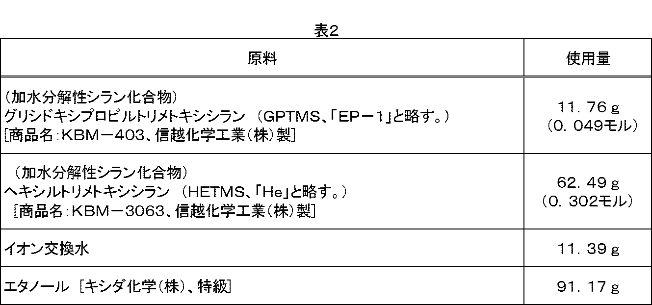

〔第2段階反応〕
次に、縮合物中間体1の8.90gを300mlのナスフラスコに入れた。更に、チタニウムi-プロポキシド(Ti-1)[高純度化学研究所製]65.11g(0.229モル)を添加し、スターラーの回転数を750rpmとして、室温で3時間攪拌して縮合物1を得た。Ti/Si比は13.0であった。
次に、縮合物中間体1の8.90gを300mlのナスフラスコに入れた。更に、チタニウムi-プロポキシド(Ti-1)[高純度化学研究所製]65.11g(0.229モル)を添加し、スターラーの回転数を750rpmとして、室温で3時間攪拌して縮合物1を得た。Ti/Si比は13.0であった。
<2.シリコーンオイルの調製>
次に、末端シラノール変性ジフェニル-ジメチル型シリコーンオイル(商品名:PDS-1615、Gelest(株)製]10gに対しメチルエチルケトン(MEK)を90g添加し、10質量%のオイル希釈品1を調製した。このフェニル変性シリコーンオイルの構造を表4に示す。
次に、末端シラノール変性ジフェニル-ジメチル型シリコーンオイル(商品名:PDS-1615、Gelest(株)製]10gに対しメチルエチルケトン(MEK)を90g添加し、10質量%のオイル希釈品1を調製した。このフェニル変性シリコーンオイルの構造を表4に示す。
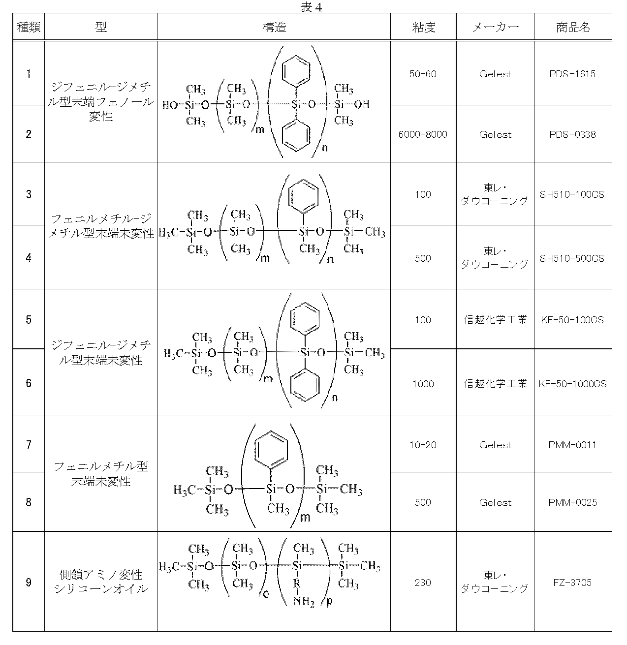
<3.表面層形成用塗料1の調製及び評価>
縮合物1の100gにオイル希釈品1を8.4g加え、さらに光カチオン重合開始剤としての芳香族スルホニウム塩[商品名:アデカオプトマー SP-150、(株)アデカ製]をメタノールで10質量%に希釈したものを3.00g添加して、混合液1-2を得た。配合比は、縮合物1:フェニル変性シリコーンオイル=100:10(質量部)である。
縮合物1の100gにオイル希釈品1を8.4g加え、さらに光カチオン重合開始剤としての芳香族スルホニウム塩[商品名:アデカオプトマー SP-150、(株)アデカ製]をメタノールで10質量%に希釈したものを3.00g添加して、混合液1-2を得た。配合比は、縮合物1:フェニル変性シリコーンオイル=100:10(質量部)である。
〔評価2〕一般式(1)の構造の確認;
次に29Si-NMR、13C-NMR測定[使用装置:JMN-EX400、JEOL社]を用いて、混合液1-2中の高分子化合物が一般式(1)の構造を有していることを確認した。測定用試料の作成方法は以下のとおりである。
次に29Si-NMR、13C-NMR測定[使用装置:JMN-EX400、JEOL社]を用いて、混合液1-2中の高分子化合物が一般式(1)の構造を有していることを確認した。測定用試料の作成方法は以下のとおりである。
先ず、アルコールで脱脂したアルミニウム製シート(厚さ:100μm)上に上記混合液1-2をスピンコートにより塗布した(使用装置;1H-D7、ミカサ(株)製)。塗布条件は回転300rpm、2秒間とした。この塗膜を乾燥した後、この塗膜に対して、254nmの波長の紫外線を積算光量が9000mJ/cm2になるように照射し、塗膜を硬化させた。紫外線の照射には、ハリソン東芝ライティング(株)製の低圧水銀ランプを用いた。得られた硬化膜をアルミニウム製シートから取り、メノウ製の乳鉢を用いて粉砕し、NMR測定用試料を調製した。この試料について29Si-NMRスペクトル、および、13C-NMRスペクトルを測定した。
29Si-NMR測定で得られたスペクトルを図5に示す。同図内にスペクトルを波形分離したピークを同時に示す。-64ppm~-74ppm付近のピークがT3成分を示す。ここでT3成分とは、有機官能基との結合を1つもつSiが、Oを介して他の原子(Si、Ti)との結合を3つ持つ状態、つまり-SiO3/2を示す。図5より、エポキシ基を有する加水分解性シラン化合物が縮合し、-SiO3/2の状態で存在する種があることを確認した。また13C-NMR測定で得られたスペクトルを図6に示す。開環前のエポキシ基を示すピークは44ppm、51ppm付近に現れ、開環重合後のピークは69ppm、72ppm付近に現れる。図6より未開環のエポキシ基がほとんど残存せずに重合していることを確認した。以上の29Si-NMR、13C-NMRのスペクトルから、縮合物1の硬化膜が一般式(1)の構造を有していることを確認した。
一方、別途、混合液1-2の固形分が1.0質量%になるようにエタノール:2-ブタノール=1:1(質量比)の混合溶媒で希釈し、表面層形成用塗料1を調製した。ここで、固形分にはシリコーンオイルに由来する成分も含まれる。
<4.帯電ローラ1の作製及び評価>
次に、導電性弾性ローラ1の弾性層の外周部に表面層形成用塗料1をリング塗布(吐出量:0.120mL/s、リング部のスピード:85mm/s、総吐出量:0.130mL)した。これに、254nmの波長の紫外線を積算光量が9000mJ/cm2になるように照射し、硬化(架橋反応による硬化)させることによって表面層を形成した。紫外線の照射には低圧水銀ランプ[ハリソン東芝ライティング(株)製]を用いた。このようにして帯電ローラ1を得た。
次に、導電性弾性ローラ1の弾性層の外周部に表面層形成用塗料1をリング塗布(吐出量:0.120mL/s、リング部のスピード:85mm/s、総吐出量:0.130mL)した。これに、254nmの波長の紫外線を積算光量が9000mJ/cm2になるように照射し、硬化(架橋反応による硬化)させることによって表面層を形成した。紫外線の照射には低圧水銀ランプ[ハリソン東芝ライティング(株)製]を用いた。このようにして帯電ローラ1を得た。
〔評価3〕塗工性;
帯電ローラ1の表面の塗工状態を目視にて以下の基準で判断した。評価結果を表11に示す。
帯電ローラ1の表面の塗工状態を目視にて以下の基準で判断した。評価結果を表11に示す。
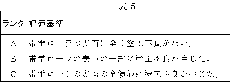
〔評価4〕表面自由エネルギー;
前述した接触角測定装置を用いて帯電ローラ1の表面自由エネルギーを測定した。評価結果(表面自由E)を表11に示す。
前述した接触角測定装置を用いて帯電ローラ1の表面自由エネルギーを測定した。評価結果(表面自由E)を表11に示す。
〔評価5〕動摩擦係数;
図4の測定機を用いて帯電ローラ1の動摩擦係数を測定した。測定条件は前述の通りである。評価結果を表11に示す。
図4の測定機を用いて帯電ローラ1の動摩擦係数を測定した。測定条件は前述の通りである。評価結果を表11に示す。
〔評価6〕Si-O-Ti結合の確認;
帯電ローラ1の表面層内のSi-O-Ti結合の存在をESCA[使用装置:Quantum2000、アルバックファイ社]により確認した。帯電ローラの表面にX線が照射されるようにし、表面層内の結合様式を評価した。検出されたO1sスペクトルより、帯電ローラの表面層内にSi-O-Ti結合の存在が確認された。
帯電ローラ1の表面層内のSi-O-Ti結合の存在をESCA[使用装置:Quantum2000、アルバックファイ社]により確認した。帯電ローラの表面にX線が照射されるようにし、表面層内の結合様式を評価した。検出されたO1sスペクトルより、帯電ローラの表面層内にSi-O-Ti結合の存在が確認された。
〔評価7〕感光体の表面電位の測定;
感光体の表面電位は、現像容器を取り外したプロセスカートリッジの現像部材の位置に、感光体に垂直になるように固定した表面電位計にて測定した。具体的には、帯電ローラ1を組み込み、表面電位計を固定したプロセスカートリッジ(商品名:「HP 35A(CB435A)」、HP社製)をレーザービームプリンター(商品名:「HP LaserJet P1006 Printer」、HP社製)に装着し、全白画像を出力した際の感光体表面電位を測定した。評価結果(感光体表面電位)を表11に示す。
感光体の表面電位は、現像容器を取り外したプロセスカートリッジの現像部材の位置に、感光体に垂直になるように固定した表面電位計にて測定した。具体的には、帯電ローラ1を組み込み、表面電位計を固定したプロセスカートリッジ(商品名:「HP 35A(CB435A)」、HP社製)をレーザービームプリンター(商品名:「HP LaserJet P1006 Printer」、HP社製)に装着し、全白画像を出力した際の感光体表面電位を測定した。評価結果(感光体表面電位)を表11に示す。
〔評価8〕帯電ローラの当接試験;
帯電ローラ1を用いて、以下のように当接試験を行った。帯電ローラ1と感光体とを、これらを一体に支持するプロセスカートリッジ(商品名:「HP 35A(CB435A)」、HP社製)に組み込んだ。このとき帯電ローラ1には合計1kgの荷重がかかるようにした。その後、高温高湿下(温度40℃、相対湿度95%)に10日間及び30日間放置した。取り出し後、常温常湿下(温度25℃、相対湿度50%)に72時間放置し、A4紙縦出力用のレーザービームプリンター(商品名:「HP LaserJet P1006 Printer」、HP社製)に装着し、出力画像を評価した。
帯電ローラ1を用いて、以下のように当接試験を行った。帯電ローラ1と感光体とを、これらを一体に支持するプロセスカートリッジ(商品名:「HP 35A(CB435A)」、HP社製)に組み込んだ。このとき帯電ローラ1には合計1kgの荷重がかかるようにした。その後、高温高湿下(温度40℃、相対湿度95%)に10日間及び30日間放置した。取り出し後、常温常湿下(温度25℃、相対湿度50%)に72時間放置し、A4紙縦出力用のレーザービームプリンター(商品名:「HP LaserJet P1006 Printer」、HP社製)に装着し、出力画像を評価した。
なお、帯電ローラ1とともにプロセスカートリッジに組み込んだ感光体は、支持体上に層厚8.0μmの有機感光層を形成してなる有機電子写真感光体である。また、この有機感光層は、支持体側から電荷発生層とポリカーボネート(結着樹脂)を含有する電荷輸送層とを積層してなる積層型感光層であり、この電荷輸送層は感光体の表面層となっている。
また、前記レーザービームプリンターに使用した現像剤(トナー)は、現像剤用結着樹脂に着色剤、荷電制御剤、離型剤、無機微粒子等を配合したもので、形式として、磁性材料を必須成分とする磁性一成分現像剤と磁性材料を含まない非磁性一成分現像剤がある。形式は現像装置に適応して適宜選択される。ここでは、磁性一成分現像剤を使用した。
帯電ローラ1の当接試験後の当接痕による、画像上のスジの評価基準(以下、「Cセットランク」という。)は以下のとおりである。以下の評価に記載している長さはA4縦用紙上での横方向のスジの長さであり、そのスジの太さはおよそ1mm程度である。評価結果を表11に示す。

〔評価9〕帯電ローラの耐付着性評価;
帯電ローラ1と感光体とを、これらを一体に支持するプロセスカートリッジ(商品名:「HP 36A(CB436A)」、HP社製)に組み込み、このプロセスカートリッジをA4紙縦出力用のレーザービームプリンター(商品名:「HP LaserJet P1505 Printer」、HP社製)に装着した。2000枚画出し後の帯電ローラ1を取り出し、目視によりトナーや外添剤の付着を調べた。画像出力は、低温低湿環境下(温度10℃、相対湿度15%)で行い、A4紙に電子写真感光体の回転方向と垂直方向に幅2ドット、間隔100スペースの横線を描く画像を形成し、1枚毎に9秒間の空回転を入れる間欠出力モードで出力した。間欠出力モードでの画像出力は、連続通紙に比べて、同じ通紙枚数でも帯電部材と感光体との摺擦回数が多くなるため、帯電部材の表面の汚れの評価に対しては、より厳しい評価である。この画像を1枚目(初期)から1000枚/日で2日(合計2000枚)出力した。
帯電ローラ1と感光体とを、これらを一体に支持するプロセスカートリッジ(商品名:「HP 36A(CB436A)」、HP社製)に組み込み、このプロセスカートリッジをA4紙縦出力用のレーザービームプリンター(商品名:「HP LaserJet P1505 Printer」、HP社製)に装着した。2000枚画出し後の帯電ローラ1を取り出し、目視によりトナーや外添剤の付着を調べた。画像出力は、低温低湿環境下(温度10℃、相対湿度15%)で行い、A4紙に電子写真感光体の回転方向と垂直方向に幅2ドット、間隔100スペースの横線を描く画像を形成し、1枚毎に9秒間の空回転を入れる間欠出力モードで出力した。間欠出力モードでの画像出力は、連続通紙に比べて、同じ通紙枚数でも帯電部材と感光体との摺擦回数が多くなるため、帯電部材の表面の汚れの評価に対しては、より厳しい評価である。この画像を1枚目(初期)から1000枚/日で2日(合計2000枚)出力した。
評価基準は以下のとおりである。評価結果(耐久後ローラ目視)を表11に示す。
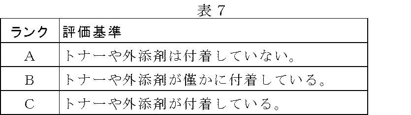
(実施例2)~(実施例38)
<1.縮合物中間体2~9の調製>
第1段階反応の原料を下記表8に記載の組成としたこと以外は実施例1の縮合物中間体1と同様にして縮合物中間体2~9を調製した。尚、表8において、記号「EP-1」~「EP-5」、「He」および「Ph」は、各々表3に記載の化合物を表している。
<1.縮合物中間体2~9の調製>
第1段階反応の原料を下記表8に記載の組成としたこと以外は実施例1の縮合物中間体1と同様にして縮合物中間体2~9を調製した。尚、表8において、記号「EP-1」~「EP-5」、「He」および「Ph」は、各々表3に記載の化合物を表している。
<2.縮合物2~38の調製>
第2段階反応の原料を表9に記載の組成としたこと以外は実施例1の縮合物1と同様にして縮合物2~38を合成した。
第2段階反応の原料を表9に記載の組成としたこと以外は実施例1の縮合物1と同様にして縮合物2~38を合成した。
<3.表面層形成用塗料2~38の調製及び評価>
縮合物2~38を用い、表10に記載の組成としたこと以外は、実施例1における混合液1-2と同様にして混合液2-2~38-2を調製した。これらの混合液を、評価2に供して、各混合液中の加水分解縮合物の硬化膜が、一般式(1)の構造を有していることを確認した。尚、表10において、シリコーンオイルの種類は、表4に記載の化合物を表している。
縮合物2~38を用い、表10に記載の組成としたこと以外は、実施例1における混合液1-2と同様にして混合液2-2~38-2を調製した。これらの混合液を、評価2に供して、各混合液中の加水分解縮合物の硬化膜が、一般式(1)の構造を有していることを確認した。尚、表10において、シリコーンオイルの種類は、表4に記載の化合物を表している。
また、混合液2-2~38-2を用いたこと以外は表面層形成用塗料1と同様にして、表面層形成用塗料2~38を調製した。
<4.帯電ローラ2~38の作製及び評価>
表面層形成用塗料2~38を用いたこと以外は、実施例1の帯電ローラ1と同様にして帯電ローラ2~38を作製し、評価3~評価9に供した。評価結果を表11に示す。
表面層形成用塗料2~38を用いたこと以外は、実施例1の帯電ローラ1と同様にして帯電ローラ2~38を作製し、評価3~評価9に供した。評価結果を表11に示す。
(比較例1)
実施例11と同様にして縮合物11を調製した。また、実施例1で使用した末端シラノール変性ジフェニル-ジメチル型シリコーンオイル1の代わりに表4に示す側鎖アミノ変性シリコーンオイル(商品名:FZー3705、東レ・ダウコーニング(株)製)を用いた。それ以外は実施例1と同様にして、表面層形成用塗料C-1を調製し、帯電ローラC-1を作製し、評価(3)~(9)に供した。評価結果を表11に示す。
実施例11と同様にして縮合物11を調製した。また、実施例1で使用した末端シラノール変性ジフェニル-ジメチル型シリコーンオイル1の代わりに表4に示す側鎖アミノ変性シリコーンオイル(商品名:FZー3705、東レ・ダウコーニング(株)製)を用いた。それ以外は実施例1と同様にして、表面層形成用塗料C-1を調製し、帯電ローラC-1を作製し、評価(3)~(9)に供した。評価結果を表11に示す。
(比較例2)
実施例1で使用した末端シラノール変性ジフェニル-ジメチル型シリコーンオイル(商品名:PDS-1615、Gelest製)をMEKで10質量%に希釈して、表面層形成用塗料C-2とした。塗工以降の操作は、実施例1と同様にして帯電ローラC-2を作製した。評価結果を表11に示す。
実施例1で使用した末端シラノール変性ジフェニル-ジメチル型シリコーンオイル(商品名:PDS-1615、Gelest製)をMEKで10質量%に希釈して、表面層形成用塗料C-2とした。塗工以降の操作は、実施例1と同様にして帯電ローラC-2を作製した。評価結果を表11に示す。

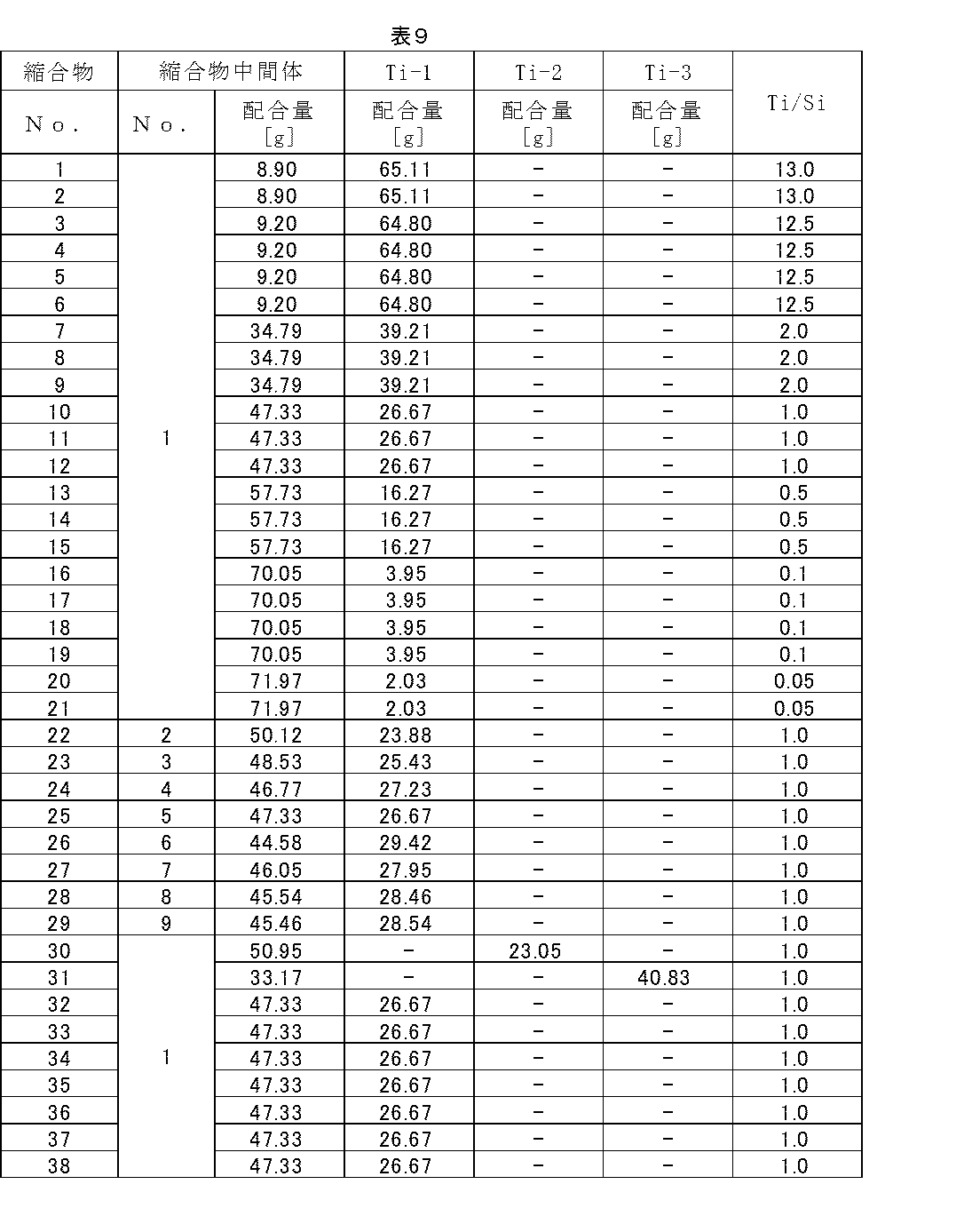
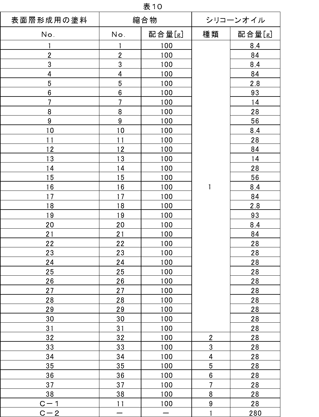

この出願は2012年6月6日に出願された日本国特許出願第2012-129061の優先権を主張するものであり、その内容を引用してこの出願の一部とするものである。
101 支持体
102 弾性層
103 表面層
102 弾性層
103 表面層
Claims (7)
- 支持体、弾性層および表面層を有している帯電部材であって、
該表面層は、
下記一般式(1)で示される構成単位と、
下記一般式(2)で示される構成単位と、
Si-O-Tiの結合を有している高分子化合物と、
下記一般式(7)~(10)で表されるフェニル変性シリコーンオイルからなる群から選択される少なくとも1つのフェニル変性シリコーンオイルと、
を含有していることを特徴とする帯電部材:



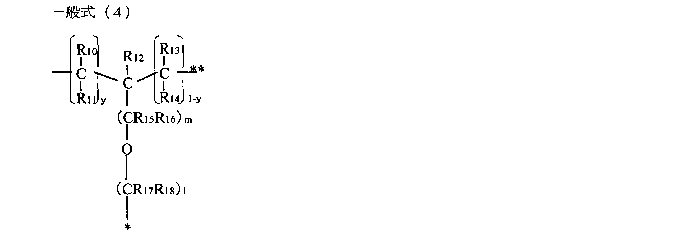

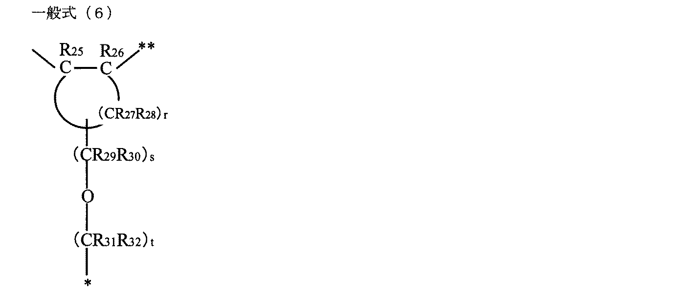
[上記R3~R7、R10~R14、R19、R20、R25およびR26は、各々独立に水素原子、炭素数1以上4以下のアルキル基、水酸基、カルボキシル基、またはアミノ基を示す。R8、R9、R15~R18、R23、R24およびR29~R32は、各々独立に水素原子、または炭素数1以上4以下のアルキル基を示す。R21、R22、R27およびR28は、各々独立に水素原子、炭素数1以上4以下のアルコキシル基、または炭素数1以上4以下のアルキル基を示す。n、m、l、q、s、およびtは、各々独立に1以上8以下の整数を示す。pおよびrは、各々独立に4以上12以下の整数を示す。xおよびyは、各々独立に0または1を示す。「*」および「**」は、各々、一般式(1)のケイ素原子および酸素原子との結合部位を示す。]、


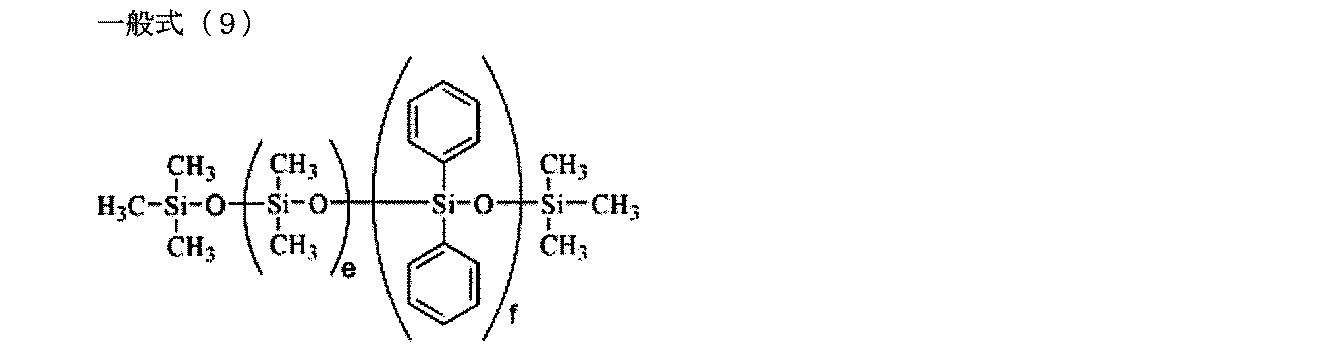
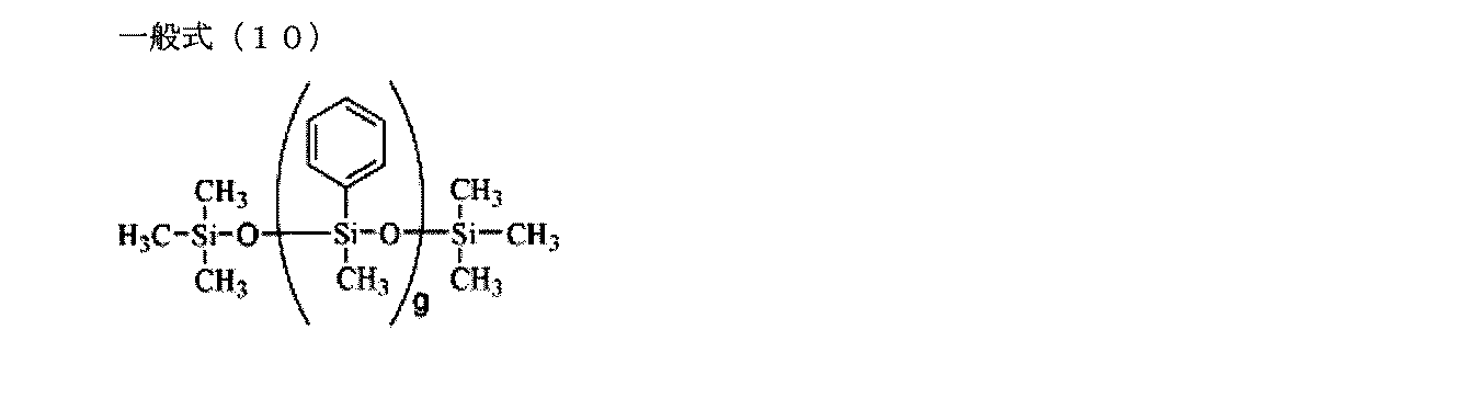
[上記一般式(7)~(10)中、a~fは、各々独立に1以上の整数を示し、a+b、c+d、およびe+fは、各々独立に2以上670以下の整数を示す。gは、1以上20以下の整数を示す。]]。 - 前記高分子化合物において、前記一般式(1)のR1およびR2が、各々独立に下記一般式(11)~(14)のいずれかで示される請求項1に記載の帯電部材:
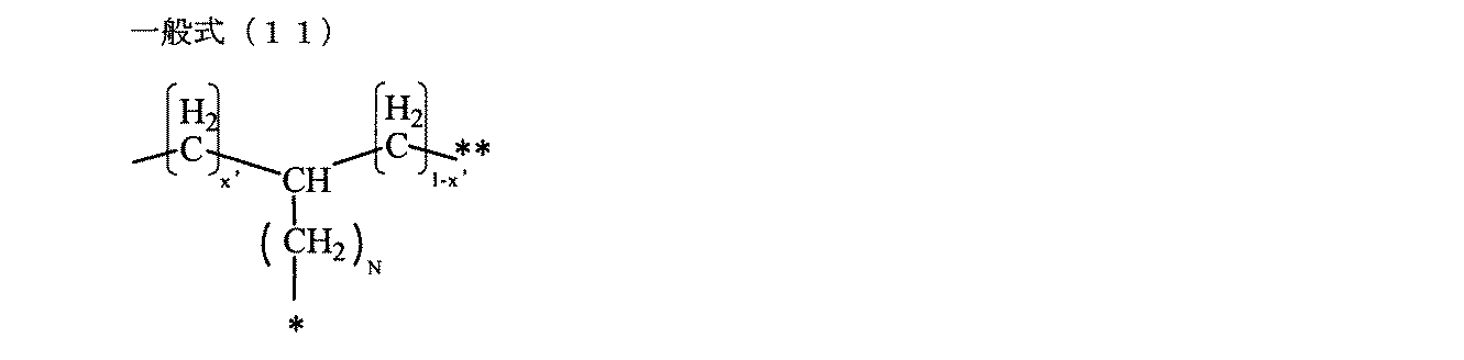
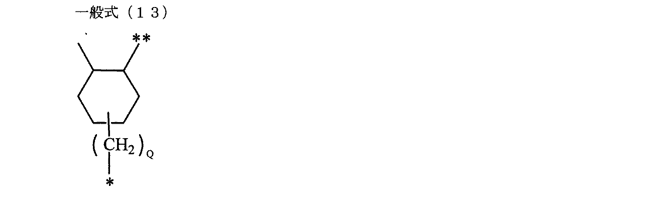
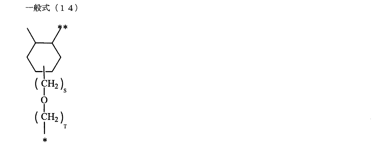
[N、M、L、Q、SおよびTは、各々独立に1以上8以下の整数を示す。x’およびy’は、各々独立に0または1を示す。「*」および「**」は、各々、一般式(1)のケイ素原子および酸素原子との結合部位を示す。]。 - 前記高分子化合物におけるチタンとケイ素との原子数比Ti/Siが0.1以上12.5以下である請求項1または2に記載の帯電部材。
- 前記高分子化合物が、下記一般式(15)で示される構造を有する加水分解性化合物の加水分解縮合物と、下記一般式(16)で示される構造を有する加水分解性化合物の加水分解縮合物との架橋物であり、かつ、一般式(7)~(10)で示されるフェニル変性シリコーンオイルのいずれかを有する請求項1~3のいずれかの一項に記載の帯電部材:

[上記一般式(15)中、R33は、下記一般式(17)~(20)のいずれかを示し、R34~R36は、各々独立に炭素数1~4のアルキル基を示す。上記一般式(16)中、R37~R40は、各々独立に炭素数1~9のアルキル基を示す;


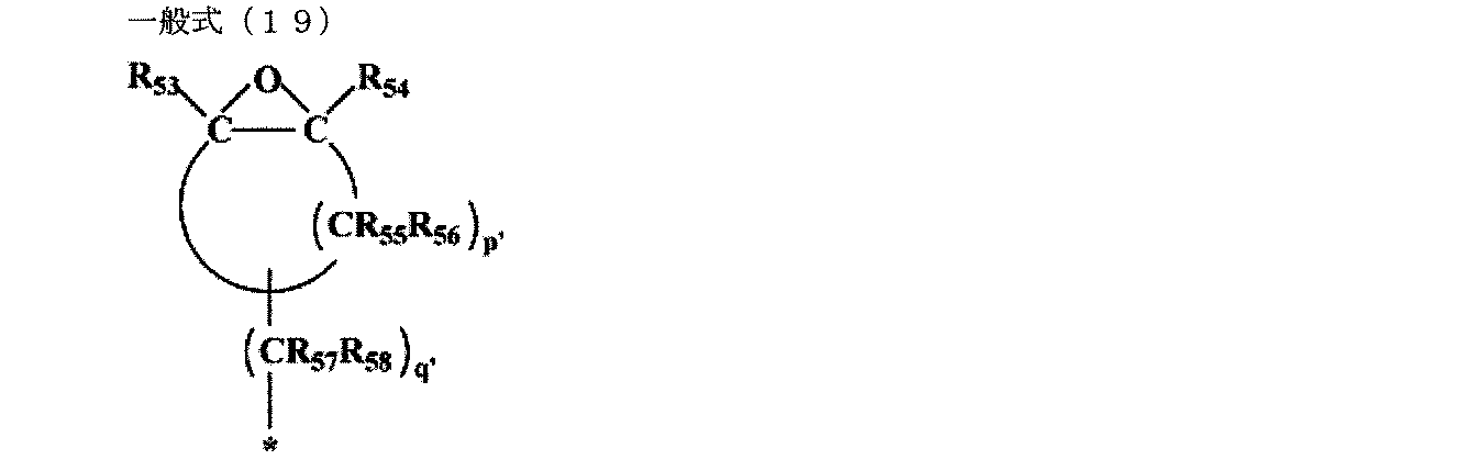
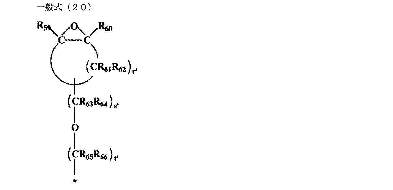
[上記一般式(17)~(20)中、R41~R43、R46~R48、R53、R54、R59およびR60は、各々独立に水素原子、炭素数1以上4以下のアルキル基、水酸基、カルボキシル基、またはアミノ基を示す。R44、R45、R49~R52、R57、R58およびR63~R66は、各々独立に水素原子、または炭素数1以上4以下のアルキル基を示す。R55、R56、R61およびR62は、各々独立に水素原子、炭素数1以上4以下のアルコキシル基、または炭素数1以上4以下のアルキル基を示す。n’、m’、l’、q’、s’およびt’は、各々独立に1以上8以下の整数を示す。p’およびr’は、各々独立に4以上12以下の整数を示す。また、「*」は、上記一般式(15)のケイ素原子との結合部位を示す。]]。 - 前記高分子化合物が、請求項4に記載の前記一般式(15)で示される構造を有する加水分解性化合物の加水分解縮合物と、前記一般式(16)で示される構造を有する加水分解性化合物の加水分解縮合物と、下記一般式(21)で示される構造を有する加水分解性化合物の加水分解縮合物との架橋物であり、かつ、一般式(7)~(10)で示されるフェニル変性シリコーンオイルのいずれかを有する請求項4に記載の帯電部材:

- 電子写真感光体と、該電子写真感光体に接触して配置されている請求項1~5のいずれかの一項に記載の帯電部材とを有することを特徴とする電子写真装置。
- 電子写真感光体と、該電子写真感光体に接触して配置されている請求項1~5のいずれかの一項に記載の帯電部材とを有し、電子写真装置の本体に着脱可能に構成されていることを特徴とするプロセスカートリッジ。
Priority Applications (2)
| Application Number | Priority Date | Filing Date | Title |
|---|---|---|---|
| CN201380029974.6A CN104380209B (zh) | 2012-06-06 | 2013-05-20 | 充电构件、处理盒和电子照相设备 |
| US14/084,148 US20140072343A1 (en) | 2012-06-06 | 2013-11-19 | Charging member, process cartridge, and electrophotographic apparatus |
Applications Claiming Priority (2)
| Application Number | Priority Date | Filing Date | Title |
|---|---|---|---|
| JP2012129061A JP5943721B2 (ja) | 2012-06-06 | 2012-06-06 | 帯電部材、プロセスカートリッジ及び電子写真装置 |
| JP2012-129061 | 2012-06-06 |
Related Child Applications (1)
| Application Number | Title | Priority Date | Filing Date |
|---|---|---|---|
| US14/084,148 Continuation US20140072343A1 (en) | 2012-06-06 | 2013-11-19 | Charging member, process cartridge, and electrophotographic apparatus |
Publications (1)
| Publication Number | Publication Date |
|---|---|
| WO2013183238A1 true WO2013183238A1 (ja) | 2013-12-12 |
Family
ID=49711646
Family Applications (1)
| Application Number | Title | Priority Date | Filing Date |
|---|---|---|---|
| PCT/JP2013/003202 Ceased WO2013183238A1 (ja) | 2012-06-06 | 2013-05-20 | 帯電部材、プロセスカートリッジ及び電子写真装置 |
Country Status (4)
| Country | Link |
|---|---|
| US (1) | US20140072343A1 (ja) |
| JP (1) | JP5943721B2 (ja) |
| CN (1) | CN104380209B (ja) |
| WO (1) | WO2013183238A1 (ja) |
Cited By (1)
| Publication number | Priority date | Publication date | Assignee | Title |
|---|---|---|---|---|
| CN106292217A (zh) * | 2015-06-26 | 2017-01-04 | 佳能株式会社 | 充电构件、处理盒和电子照相图像形成设备 |
Families Citing this family (32)
| Publication number | Priority date | Publication date | Assignee | Title |
|---|---|---|---|---|
| WO2015098117A1 (ja) | 2013-12-27 | 2015-07-02 | キヤノン株式会社 | 帯電部材、プロセスカートリッジ及び電子写真画像形成装置 |
| US9442408B2 (en) | 2014-11-28 | 2016-09-13 | Canon Kabushiki Kaisha | Member for electrophotography, method for producing the same, and image forming apparatus |
| US9897931B2 (en) | 2014-11-28 | 2018-02-20 | Canon Kabushiki Kaisha | Electroconductive member for electrophotography, process cartridge, and electrophotographic image-forming apparatus |
| US9360789B1 (en) | 2014-11-28 | 2016-06-07 | Canon Kabushiki Kaisha | Member for electrophotography, process cartridge and image forming apparatus |
| US9921513B2 (en) * | 2014-12-09 | 2018-03-20 | Canon Kabushiki Kaisha | Charging member, process cartridge, and electrophotographic apparatus |
| US10078286B2 (en) | 2015-04-10 | 2018-09-18 | Canon Kabushiki Kaisha | Charging member, process cartridge and electrophotographic apparatus |
| US9989879B2 (en) | 2015-06-26 | 2018-06-05 | Canon Kabushiki Kaisha | Charging member, process cartridge and electrophotographic image forming apparatus |
| US9740133B2 (en) | 2015-09-30 | 2017-08-22 | Canon Kabushiki Kaisha | Charging member, process cartridge and electrophotographic image forming apparatus |
| US10678158B2 (en) | 2016-09-26 | 2020-06-09 | Canon Kabushiki Kaisha | Electro-conductive member for electrophotography, process cartridge, and electrophotographic image forming apparatus |
| JP6976774B2 (ja) | 2016-09-27 | 2021-12-08 | キヤノン株式会社 | 電子写真用導電性部材、プロセスカートリッジおよび電子写真画像形成装置 |
| US10459356B2 (en) | 2016-10-07 | 2019-10-29 | Canon Kabushiki Kaisha | Charging member, process cartridge and electrophotographic image forming apparatus |
| US10416588B2 (en) | 2016-10-31 | 2019-09-17 | Canon Kabushiki Kaisha | Charging member, process cartridge, electrophotographic image forming apparatus, and method for manufacturing charging member |
| JP6784589B2 (ja) | 2016-12-21 | 2020-11-11 | キヤノン株式会社 | 帯電部材、帯電部材の製造方法、プロセスカートリッジおよび電子写真画像形成装置 |
| CN110192156B (zh) * | 2017-01-20 | 2022-10-11 | 惠普深蓝有限责任公司 | 用于液体电子照相印刷的显影器辊 |
| US10248042B2 (en) | 2017-06-02 | 2019-04-02 | Canon Kabushiki Kaisha | Electrophotographic roller, process cartridge and electrophotographic apparatus |
| WO2019203225A1 (ja) | 2018-04-18 | 2019-10-24 | キヤノン株式会社 | 導電性部材、プロセスカートリッジ及び電子写真画像形成装置 |
| WO2019203227A1 (ja) | 2018-04-18 | 2019-10-24 | キヤノン株式会社 | 導電性部材、プロセスカートリッジ、および画像形成装置 |
| CN112020678B (zh) | 2018-04-18 | 2022-11-01 | 佳能株式会社 | 导电性构件、处理盒和电子照相图像形成设备 |
| CN112005173B (zh) | 2018-04-18 | 2023-03-24 | 佳能株式会社 | 导电性构件、处理盒和图像形成设备 |
| US10747130B2 (en) * | 2018-05-31 | 2020-08-18 | Canon Kabushiki Kaisha | Process cartridge and electrophotographic apparatus |
| JP7336289B2 (ja) | 2018-07-31 | 2023-08-31 | キヤノン株式会社 | 電子写真用部材、電子写真プロセスカートリッジ及び電子写真画像形成装置 |
| JP7114409B2 (ja) | 2018-08-31 | 2022-08-08 | キヤノン株式会社 | 現像ローラ、電子写真プロセスカートリッジおよび電子写真画像形成装置 |
| JP7446878B2 (ja) | 2019-03-29 | 2024-03-11 | キヤノン株式会社 | 導電性部材、電子写真用プロセスカートリッジ、及び電子写真画像形成装置 |
| US11169454B2 (en) | 2019-03-29 | 2021-11-09 | Canon Kabushiki Kaisha | Electrophotographic electro-conductive member, process cartridge, and electrophotographic image forming apparatus |
| JP7401256B2 (ja) | 2019-10-18 | 2023-12-19 | キヤノン株式会社 | 電子写真装置、プロセスカートリッジ及びカートリッジセット |
| JP7669134B2 (ja) | 2019-10-18 | 2025-04-28 | キヤノン株式会社 | 導電性部材、プロセスカートリッジ並びに電子写真画像形成装置 |
| JP7321884B2 (ja) | 2019-10-18 | 2023-08-07 | キヤノン株式会社 | 電子写真装置、プロセスカートリッジ及びカートリッジセット |
| JP7404026B2 (ja) | 2019-10-18 | 2023-12-25 | キヤノン株式会社 | 電子写真装置、プロセスカートリッジ、及びカートリッジセット |
| JP7330852B2 (ja) | 2019-10-18 | 2023-08-22 | キヤノン株式会社 | 電子写真装置、プロセスカートリッジ、及びカートリッジセット |
| JP7401255B2 (ja) | 2019-10-18 | 2023-12-19 | キヤノン株式会社 | 電子写真装置、プロセスカートリッジ、及びカートリッジセット |
| JP7330851B2 (ja) | 2019-10-18 | 2023-08-22 | キヤノン株式会社 | 電子写真装置、プロセスカートリッジ、及びカートリッジセット |
| JP7599920B2 (ja) | 2020-11-17 | 2024-12-16 | キヤノン株式会社 | 現像装置 |
Citations (6)
| Publication number | Priority date | Publication date | Assignee | Title |
|---|---|---|---|---|
| JPH06242662A (ja) * | 1993-02-19 | 1994-09-02 | Fuji Xerox Co Ltd | 電子写真用帯電ロール |
| JP2002214876A (ja) * | 2001-01-12 | 2002-07-31 | Bridgestone Corp | 帯電部材及び帯電装置 |
| JP2003316123A (ja) * | 2002-04-26 | 2003-11-06 | Canon Chemicals Inc | 帯電ローラ |
| JP2009058635A (ja) * | 2007-08-30 | 2009-03-19 | Canon Inc | 帯電部材、プロセスカートリッジおよび電子写真装置 |
| JP2011154353A (ja) * | 2009-12-28 | 2011-08-11 | Canon Inc | 帯電部材、プロセスカートリッジ及び電子写真装置 |
| JP2012063759A (ja) * | 2010-08-19 | 2012-03-29 | Canon Inc | 帯電部材、プロセスカートリッジ及び電子写真装置 |
Family Cites Families (8)
| Publication number | Priority date | Publication date | Assignee | Title |
|---|---|---|---|---|
| US6309754B1 (en) * | 1995-09-29 | 2001-10-30 | Nexpress Solutions Llc | Fusing members having copper oxide-filled, addition-cured siloxane layers |
| JP3925508B2 (ja) * | 2004-04-28 | 2007-06-06 | コニカミノルタビジネステクノロジーズ株式会社 | 転写ベルトおよび該ベルトを有する画像形成装置 |
| CN100570502C (zh) * | 2004-12-28 | 2009-12-16 | 佳能株式会社 | 充电构件、处理盒和电子照相设备 |
| JP2006293004A (ja) * | 2005-04-11 | 2006-10-26 | Canon Chemicals Inc | 電子写真用帯電ローラ |
| JP5100148B2 (ja) * | 2006-02-28 | 2012-12-19 | キヤノン株式会社 | 帯電部材、プロセスカートリッジおよび電子写真装置 |
| WO2010050615A1 (ja) * | 2008-10-31 | 2010-05-06 | キヤノン株式会社 | 帯電部材、プロセスカートリッジ及び電子写真装置 |
| JP5729988B2 (ja) * | 2009-12-15 | 2015-06-03 | キヤノン株式会社 | 帯電部材、プロセスカートリッジ及び電子写真装置 |
| JP2011137109A (ja) * | 2009-12-28 | 2011-07-14 | Canon Inc | ポリシロキサン含有膜形成用の組成物及び帯電部材 |
-
2012
- 2012-06-06 JP JP2012129061A patent/JP5943721B2/ja not_active Expired - Fee Related
-
2013
- 2013-05-20 CN CN201380029974.6A patent/CN104380209B/zh not_active Expired - Fee Related
- 2013-05-20 WO PCT/JP2013/003202 patent/WO2013183238A1/ja not_active Ceased
- 2013-11-19 US US14/084,148 patent/US20140072343A1/en not_active Abandoned
Patent Citations (6)
| Publication number | Priority date | Publication date | Assignee | Title |
|---|---|---|---|---|
| JPH06242662A (ja) * | 1993-02-19 | 1994-09-02 | Fuji Xerox Co Ltd | 電子写真用帯電ロール |
| JP2002214876A (ja) * | 2001-01-12 | 2002-07-31 | Bridgestone Corp | 帯電部材及び帯電装置 |
| JP2003316123A (ja) * | 2002-04-26 | 2003-11-06 | Canon Chemicals Inc | 帯電ローラ |
| JP2009058635A (ja) * | 2007-08-30 | 2009-03-19 | Canon Inc | 帯電部材、プロセスカートリッジおよび電子写真装置 |
| JP2011154353A (ja) * | 2009-12-28 | 2011-08-11 | Canon Inc | 帯電部材、プロセスカートリッジ及び電子写真装置 |
| JP2012063759A (ja) * | 2010-08-19 | 2012-03-29 | Canon Inc | 帯電部材、プロセスカートリッジ及び電子写真装置 |
Cited By (2)
| Publication number | Priority date | Publication date | Assignee | Title |
|---|---|---|---|---|
| CN106292217A (zh) * | 2015-06-26 | 2017-01-04 | 佳能株式会社 | 充电构件、处理盒和电子照相图像形成设备 |
| CN106292217B (zh) * | 2015-06-26 | 2019-07-23 | 佳能株式会社 | 充电构件、处理盒和电子照相图像形成设备 |
Also Published As
| Publication number | Publication date |
|---|---|
| CN104380209B (zh) | 2016-09-28 |
| JP5943721B2 (ja) | 2016-07-05 |
| JP2013254069A (ja) | 2013-12-19 |
| US20140072343A1 (en) | 2014-03-13 |
| CN104380209A (zh) | 2015-02-25 |
Similar Documents
| Publication | Publication Date | Title |
|---|---|---|
| JP5943721B2 (ja) | 帯電部材、プロセスカートリッジ及び電子写真装置 | |
| JP4954344B2 (ja) | 帯電部材及びその製造方法 | |
| JP4948668B2 (ja) | 帯電部材、プロセスカートリッジ及び電子写真装置 | |
| JP5943690B2 (ja) | 帯電部材、プロセスカートリッジ及び電子写真装置 | |
| JP5843646B2 (ja) | 帯電部材、その製法、プロセスカートリッジ及び電子写真装置 | |
| JP5038524B2 (ja) | 帯電部材、プロセスカートリッジおよび電子写真装置 | |
| JP5925051B2 (ja) | 帯電部材、プロセスカートリッジ及び電子写真装置 | |
| JP4948666B2 (ja) | 帯電部材及びその製造方法 | |
| JP4942233B2 (ja) | 帯電部材、プロセスカートリッジおよび電子写真装置 | |
| WO2012147301A1 (ja) | 帯電部材、プロセスカートリッジ、電子写真装置、及び帯電部材の製造方法 | |
| JP4841016B1 (ja) | 帯電部材、プロセスカートリッジ及び電子写真装置 | |
| WO2011080906A1 (ja) | 帯電部材、プロセスカートリッジ及び電子写真装置 | |
| WO2012042765A1 (ja) | 帯電部材、プロセスカートリッジおよび電子写真装置 | |
| JP4942234B2 (ja) | 帯電部材、その製造方法及び電子写真装置 | |
| JP5279218B2 (ja) | 帯電部材、プロセスカートリッジおよび電子写真装置 |
Legal Events
| Date | Code | Title | Description |
|---|---|---|---|
| 121 | Ep: the epo has been informed by wipo that ep was designated in this application |
Ref document number: 13801332 Country of ref document: EP Kind code of ref document: A1 |
|
| NENP | Non-entry into the national phase |
Ref country code: DE |
|
| 122 | Ep: pct application non-entry in european phase |
Ref document number: 13801332 Country of ref document: EP Kind code of ref document: A1 |