WO2013168795A1 - 半導体装置 - Google Patents
半導体装置 Download PDFInfo
- Publication number
- WO2013168795A1 WO2013168795A1 PCT/JP2013/063157 JP2013063157W WO2013168795A1 WO 2013168795 A1 WO2013168795 A1 WO 2013168795A1 JP 2013063157 W JP2013063157 W JP 2013063157W WO 2013168795 A1 WO2013168795 A1 WO 2013168795A1
- Authority
- WO
- WIPO (PCT)
- Prior art keywords
- upper electrode
- respect
- semiconductor layer
- ring
- region
- Prior art date
- Legal status (The legal status is an assumption and is not a legal conclusion. Google has not performed a legal analysis and makes no representation as to the accuracy of the status listed.)
- Ceased
Links
Images




Classifications
-
- H—ELECTRICITY
- H10—SEMICONDUCTOR DEVICES; ELECTRIC SOLID-STATE DEVICES NOT OTHERWISE PROVIDED FOR
- H10D—INORGANIC ELECTRIC SEMICONDUCTOR DEVICES
- H10D62/00—Semiconductor bodies, or regions thereof, of devices having potential barriers
- H10D62/10—Shapes, relative sizes or dispositions of the regions of the semiconductor bodies; Shapes of the semiconductor bodies
- H10D62/113—Isolations within a component, i.e. internal isolations
- H10D62/114—PN junction isolations
-
- H—ELECTRICITY
- H10—SEMICONDUCTOR DEVICES; ELECTRIC SOLID-STATE DEVICES NOT OTHERWISE PROVIDED FOR
- H10D—INORGANIC ELECTRIC SEMICONDUCTOR DEVICES
- H10D30/00—Field-effect transistors [FET]
- H10D30/60—Insulated-gate field-effect transistors [IGFET]
- H10D30/64—Double-diffused metal-oxide semiconductor [DMOS] FETs
- H10D30/66—Vertical DMOS [VDMOS] FETs
- H10D30/665—Vertical DMOS [VDMOS] FETs having edge termination structures
-
- H—ELECTRICITY
- H10—SEMICONDUCTOR DEVICES; ELECTRIC SOLID-STATE DEVICES NOT OTHERWISE PROVIDED FOR
- H10D—INORGANIC ELECTRIC SEMICONDUCTOR DEVICES
- H10D62/00—Semiconductor bodies, or regions thereof, of devices having potential barriers
- H10D62/40—Crystalline structures
- H10D62/405—Orientations of crystalline planes
-
- H—ELECTRICITY
- H10—SEMICONDUCTOR DEVICES; ELECTRIC SOLID-STATE DEVICES NOT OTHERWISE PROVIDED FOR
- H10D—INORGANIC ELECTRIC SEMICONDUCTOR DEVICES
- H10D62/00—Semiconductor bodies, or regions thereof, of devices having potential barriers
- H10D62/80—Semiconductor bodies, or regions thereof, of devices having potential barriers characterised by the materials
- H10D62/83—Semiconductor bodies, or regions thereof, of devices having potential barriers characterised by the materials being Group IV materials, e.g. B-doped Si or undoped Ge
- H10D62/8303—Diamond
-
- H—ELECTRICITY
- H10—SEMICONDUCTOR DEVICES; ELECTRIC SOLID-STATE DEVICES NOT OTHERWISE PROVIDED FOR
- H10D—INORGANIC ELECTRIC SEMICONDUCTOR DEVICES
- H10D62/00—Semiconductor bodies, or regions thereof, of devices having potential barriers
- H10D62/80—Semiconductor bodies, or regions thereof, of devices having potential barriers characterised by the materials
- H10D62/83—Semiconductor bodies, or regions thereof, of devices having potential barriers characterised by the materials being Group IV materials, e.g. B-doped Si or undoped Ge
- H10D62/832—Semiconductor bodies, or regions thereof, of devices having potential barriers characterised by the materials being Group IV materials, e.g. B-doped Si or undoped Ge being Group IV materials comprising two or more elements, e.g. SiGe
- H10D62/8325—Silicon carbide
-
- H—ELECTRICITY
- H10—SEMICONDUCTOR DEVICES; ELECTRIC SOLID-STATE DEVICES NOT OTHERWISE PROVIDED FOR
- H10D—INORGANIC ELECTRIC SEMICONDUCTOR DEVICES
- H10D62/00—Semiconductor bodies, or regions thereof, of devices having potential barriers
- H10D62/80—Semiconductor bodies, or regions thereof, of devices having potential barriers characterised by the materials
- H10D62/85—Semiconductor bodies, or regions thereof, of devices having potential barriers characterised by the materials being Group III-V materials, e.g. GaAs
- H10D62/8503—Nitride Group III-V materials, e.g. AlN or GaN
-
- H—ELECTRICITY
- H10—SEMICONDUCTOR DEVICES; ELECTRIC SOLID-STATE DEVICES NOT OTHERWISE PROVIDED FOR
- H10D—INORGANIC ELECTRIC SEMICONDUCTOR DEVICES
- H10D64/00—Electrodes of devices having potential barriers
- H10D64/20—Electrodes characterised by their shapes, relative sizes or dispositions
- H10D64/23—Electrodes carrying the current to be rectified, amplified, oscillated or switched, e.g. sources, drains, anodes or cathodes
- H10D64/251—Source or drain electrodes for field-effect devices
- H10D64/252—Source or drain electrodes for field-effect devices for vertical or pseudo-vertical devices
-
- H—ELECTRICITY
- H10—SEMICONDUCTOR DEVICES; ELECTRIC SOLID-STATE DEVICES NOT OTHERWISE PROVIDED FOR
- H10D—INORGANIC ELECTRIC SEMICONDUCTOR DEVICES
- H10D64/00—Electrodes of devices having potential barriers
- H10D64/20—Electrodes characterised by their shapes, relative sizes or dispositions
- H10D64/23—Electrodes carrying the current to be rectified, amplified, oscillated or switched, e.g. sources, drains, anodes or cathodes
- H10D64/251—Source or drain electrodes for field-effect devices
- H10D64/258—Source or drain electrodes for field-effect devices characterised by the relative positions of the source or drain electrodes with respect to the gate electrode
-
- H—ELECTRICITY
- H10—SEMICONDUCTOR DEVICES; ELECTRIC SOLID-STATE DEVICES NOT OTHERWISE PROVIDED FOR
- H10P—GENERIC PROCESSES OR APPARATUS FOR THE MANUFACTURE OR TREATMENT OF DEVICES COVERED BY CLASS H10
- H10P30/00—Ion implantation into wafers, substrates or parts of devices
- H10P30/20—Ion implantation into wafers, substrates or parts of devices into semiconductor materials, e.g. for doping
- H10P30/202—Ion implantation into wafers, substrates or parts of devices into semiconductor materials, e.g. for doping characterised by the semiconductor materials
- H10P30/204—Ion implantation into wafers, substrates or parts of devices into semiconductor materials, e.g. for doping characterised by the semiconductor materials into Group IV semiconductors
- H10P30/2042—Ion implantation into wafers, substrates or parts of devices into semiconductor materials, e.g. for doping characterised by the semiconductor materials into Group IV semiconductors into crystalline silicon carbide
-
- H—ELECTRICITY
- H10—SEMICONDUCTOR DEVICES; ELECTRIC SOLID-STATE DEVICES NOT OTHERWISE PROVIDED FOR
- H10P—GENERIC PROCESSES OR APPARATUS FOR THE MANUFACTURE OR TREATMENT OF DEVICES COVERED BY CLASS H10
- H10P30/00—Ion implantation into wafers, substrates or parts of devices
- H10P30/20—Ion implantation into wafers, substrates or parts of devices into semiconductor materials, e.g. for doping
- H10P30/21—Ion implantation into wafers, substrates or parts of devices into semiconductor materials, e.g. for doping of electrically active species
-
- H—ELECTRICITY
- H10—SEMICONDUCTOR DEVICES; ELECTRIC SOLID-STATE DEVICES NOT OTHERWISE PROVIDED FOR
- H10D—INORGANIC ELECTRIC SEMICONDUCTOR DEVICES
- H10D62/00—Semiconductor bodies, or regions thereof, of devices having potential barriers
- H10D62/10—Shapes, relative sizes or dispositions of the regions of the semiconductor bodies; Shapes of the semiconductor bodies
- H10D62/102—Constructional design considerations for preventing surface leakage or controlling electric field concentration
- H10D62/103—Constructional design considerations for preventing surface leakage or controlling electric field concentration for increasing or controlling the breakdown voltage of reverse-biased devices
- H10D62/105—Constructional design considerations for preventing surface leakage or controlling electric field concentration for increasing or controlling the breakdown voltage of reverse-biased devices by having particular doping profiles, shapes or arrangements of PN junctions; by having supplementary regions, e.g. junction termination extension [JTE]
- H10D62/106—Constructional design considerations for preventing surface leakage or controlling electric field concentration for increasing or controlling the breakdown voltage of reverse-biased devices by having particular doping profiles, shapes or arrangements of PN junctions; by having supplementary regions, e.g. junction termination extension [JTE] having supplementary regions doped oppositely to or in rectifying contact with regions of the semiconductor bodies, e.g. guard rings with PN or Schottky junctions
Definitions
- the present invention relates to a semiconductor device.
- Patent Document 1 discloses an n drift layer stacked on an n + drain layer, a p base region formed in a surface layer of the n drift layer, an n + source region formed in the p base region, On the surface of the p base region sandwiched between the high concentration p + well region formed overlapping the p base region, the n + source region and the surface exposed portion of the n drift layer, via a gate oxide film Insulating the gate electrode layer provided, the source electrode in common contact with the n + source region and the p + well region, the drain electrode provided on the back surface of the n + drain layer, and the gate electrode layer and the source electrode An SiC vertical MOSFET including an interlayer insulating film is disclosed.
- a semiconductor device includes a first conductivity type semiconductor layer having an active region in which a semiconductor element is formed, and a surface portion of the semiconductor layer along an outer periphery of the active region.
- a termination structure of a second conductivity type, and an upper electrode formed on the semiconductor layer via an insulating film and selectively penetrating the insulating film and connected to the termination structure,
- a high strength region having a relatively high dielectric breakdown strength and a low strength region having a relatively low dielectric breakdown strength compared to the high strength region, and the shape of the high strength region and the shape of the low strength region are Are asymmetric with each other (Claim 1).
- the shape of the low-intensity region is made difficult to concentrate the electric field, and the shape of the low-intensity region and the shape of the high-intensity region are asymmetrical with each other. Etc.) can be prevented from being broken.
- the respective shapes are designed so that the avalanche breakdown occurs simultaneously in the low-intensity region and the high-intensity region, the avalanche current can be made to flow evenly in each region.
- a semiconductor device includes a first conductivity type semiconductor layer having an active region in which a semiconductor element is formed, and a surface portion of the semiconductor layer along the outer periphery of the active region.
- a second conductivity type termination structure having a high strength region having a relatively high dielectric breakdown strength and a low strength region having a relatively low dielectric breakdown strength compared to the high strength region, and an insulating film
- An upper electrode formed on the semiconductor layer and selectively passing through the insulating film and connected to the high-strength region and the low-strength region; and a contact area of the upper electrode with respect to the high-strength region; The contact areas of the upper electrode with respect to the low-strength region are different from each other (Claim 2).
- the contact area of the upper electrode with respect to the low-strength region is reduced by increasing the contact area of the upper electrode with respect to the low-strength region to be different from the contact area of the upper electrode with respect to the high-strength region. can do. Thereby, excessive heat generation in the low strength region can be prevented, and thermal destruction can be prevented. As a result, the avalanche resistance can be improved.
- the semiconductor layer may be made of a semiconductor material having plane orientation dependency with respect to dielectric breakdown strength.
- the semiconductor material may contain SiC, GaN, or diamond.
- a semiconductor device according to a third aspect of the present invention is composed of a first conductivity type SiC having a surface inclined at a predetermined off angle ⁇ with respect to the (0001) plane, and has an active region in which a semiconductor element is formed.
- An upper electrode selectively penetrating the membrane and connected to the termination structure, the termination structure including a first side and a second side facing each other in a ⁇ 11-20> direction in plan view,
- the tangent to the outer peripheral end of the first side extends in a direction crossing the ⁇ 11-20> direction, and the tangent to the outer peripheral end of the second side extends in a direction along the ⁇ 11-20> direction, First side length
- the radius of curvature of the corners of direction both end portions is greater than the radius of curvature of the corners of the longitudinal ends of the second side (claim 5).
- the dielectric breakdown strength of SiC depends on the plane orientation of SiC. For example, when the ⁇ 0001> direction is compared with the ⁇ 11-20> direction orthogonal to the ⁇ 0001> direction, the ⁇ 11-20> direction has lower dielectric breakdown strength than the ⁇ 0001> direction. Therefore, even when an electric field of the same magnitude is applied, if the direction of the electric field is the ⁇ 0001> direction, SiC is not easily destroyed. On the other hand, if the direction of the electric field is the ⁇ 11-20> direction, compared to the former. SiC is easily destroyed.
- the tangent to the outer peripheral end of the first side extends in a direction crossing the ⁇ 11-20> direction
- the tangent to the outer peripheral end of the second side is ⁇ 11-20>. It extends in a direction along the direction.
- An electric field is applied to the outer peripheral edge of each side in a direction intersecting with each tangent.
- an electric field is applied to the outer peripheral edge of the first side in the direction intersecting the tangent (direction along the ⁇ 11-20> direction), and the outer edge of the second side is intersected with the tangent ( ⁇ 11- Electric field is applied in the direction intersecting the 20> direction.
- the first side where the electric field is applied in the direction along the ⁇ 11-20> direction is more susceptible to SiC breakdown than the second side where the electric field is applied in the direction intersecting the ⁇ 11-20> direction. Therefore, of the corners of the first side and the second side where the electric field tends to concentrate in a high electric field state (for example, avalanche resistance test etc.), the corner of the first side having a relatively low dielectric breakdown strength is broken. There is a risk.
- the radius of curvature of the corners at both ends in the longitudinal direction of the first side is larger than the radius of curvature of the corners at both ends in the longitudinal direction of the second side, the electric field to the corners of the first side Concentration can be eased. Therefore, it is possible to prevent the corner portion of the first side from being broken in a high electric field state.
- each radius of curvature is designed so that avalanche breakdown occurs at the corners of the first side and the second side at the same time, the avalanche current may flow evenly through the first and second sides. it can.
- the upper electrode is connected to the first side and the second side, and a contact area of the upper electrode with respect to the first side is equal to the second side. It is preferable that it is larger than the contact area of the upper electrode.
- the contact resistance of the upper electrode with respect to the first side can be reduced by increasing the contact area of the upper electrode with respect to the first side. Thereby, excessive heat generation in the first side can be prevented, and thermal destruction can be prevented. As a result, the avalanche resistance can be improved.
- the upper electrode is connected to the first side and the second side, and a contact area of the upper electrode with respect to the first side and the second side
- the contact area of the upper electrode with respect to may be equal to each other (claim 7).
- the semiconductor device according to the third aspect includes a plurality of second conductivity type guard rings formed outside the semiconductor layer with respect to the termination structure and electrically floating with respect to the upper electrode.
- the plurality of guard rings face each other in the ⁇ 11-20> direction in plan view, and include a ring first side close to the first side and a ring second side close to the second side,
- the tangent to the outer peripheral edge of the first ring side extends in a direction crossing the ⁇ 11-20> direction, and the tangent to the outer peripheral edge of the second ring side extends in a direction along the ⁇ 11-20> direction.
- the pitch of the line and space pattern on the first side of the ring is preferably narrower than the pitch of the line and space pattern on the second side of the ring.
- a semiconductor device is made of SiC of the first conductivity type having a surface inclined at a predetermined off angle ⁇ with respect to the (0001) plane, and has an active region in which a semiconductor element is formed.
- a second conductive layer including a semiconductor layer and a first side and a second side formed in a square ring along the outer periphery of the active region on the surface portion of the semiconductor layer and facing each other in a ⁇ 11-20> direction in a plan view;
- a sectional structure including a mold termination structure and an upper electrode formed on the semiconductor layer via an insulating film and selectively penetrating the insulating film and connected to the first side and the second side.
- the tangent to the outer peripheral end of the first side extends in a direction crossing the ⁇ 11-20> direction, and the tangent to the outer peripheral end of the second side extends in a direction along the ⁇ 11-20> direction, Before the first side The contact area of the upper electrode is larger than the contact area of the upper electrode with respect to said second side (claim 9).
- a semiconductor device includes an active region made of SiC of the first conductivity type having a surface inclined at a predetermined off angle ⁇ with respect to the (0001) plane, and in which a semiconductor element is formed.
- a plurality of second-conductivity type guard rings that are floating in a floating manner, the plurality of guard rings including a first ring side and a second ring side facing each other in a ⁇ 11-20> direction in plan view, In view, the tangent to the outer peripheral edge of the first side of the ring extends in a direction crossing the ⁇ 11-20> direction, and the tangent to the outer peripheral edge of the second side of the ring is along the ⁇ 11-20> direction.
- the pitch of the line-and-space pattern of the ring first side is narrower than the pitch of the line-and-space pattern of the ring second side (claim 10).
- the depletion layers generated by the junction of each ring first side and the semiconductor layer can be continuously connected and spread, so The electric field can be relaxed.
- FIG. 1 is a schematic plan view of a semiconductor device according to the first embodiment of the present invention.
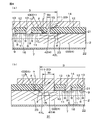
- 2A and 2B are cross-sectional views of the semiconductor device, in which FIG. 2A is a cross-sectional view taken along a cutting line IIa-IIa in FIG. 1, and FIG. 2B is a cutting line in FIG. The cut surfaces at IIb-IIb are shown respectively.
- FIG. 3 is a schematic plan view of a semiconductor device according to the second embodiment of the present invention.
- 4 (a) and 4 (b) are cross-sectional views of the semiconductor device, in which FIG. 4 (a) is a cut surface taken along the cutting line IVa-IVa in FIG. 3, and FIG. 4 (b) is a cutting line in FIG.
- FIG. 5 is a schematic plan view of a semiconductor device according to the third embodiment of the present invention.
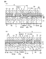
- 6 (a) and 6 (b) are cross-sectional views of the semiconductor device, in which FIG. 6 (a) is a cut surface taken along the cutting line VIa-VIa of FIG. 5, and FIG. 6 (b) is a cutting line of FIG.
- the cut surfaces at VIb-VIb are shown respectively.
- FIG. 7 is a schematic plan view of a semiconductor device according to the fourth embodiment of the present invention.
- 8A and 8B are cross-sectional views of the semiconductor device, in which FIG. 8A is a cut surface taken along the cutting line VIIIa-VIIIa of FIG. 7, and FIG. 8B is a cutting line of FIG.
- the cut surfaces at VIIIb-VIIIb are shown respectively.
- FIG. 1 is a schematic plan view of a semiconductor device according to the first embodiment of the present invention.
- the semiconductor device 1 is a power MOSFET (Metal-Oxide-Semiconductor) using SiC (silicon carbide).
- Field Effect Transistor) elements (individual elements), for example, the length in the vertical direction on the paper surface of FIG. 1 is about 1 mm.
- the semiconductor device 1 includes an active region 3 that is disposed at a central portion on an SiC substrate 2 as an example of a semiconductor layer and functions as a field effect transistor.
- a square annular termination structure 4 is formed on the peripheral edge of the active region 3 along the outer periphery thereof.
- 2A and 2B are cross-sectional views of the semiconductor device, in which FIG. 2A is a cross-sectional view taken along a cutting line IIa-IIa in FIG. 1, and FIG. 2B is a cutting line in FIG. The cut surfaces at IIb-IIb are shown respectively.
- the semiconductor device 1 is a so-called DMOS (Double-Diffusion). (Metal-Oxide-Semiconductor) structure.
- DMOS Double-Diffusion
- the double diffusion technique cannot be applied, and a device having a DMOS structure is manufactured by double-implantation.
- the SiC substrate 2 is n-type and functions as a drain region of the field effect transistor.
- the SiC substrate 2 will be specifically described.
- the SiC constituting the SiC substrate 2 is a material exhibiting a crystal polymorph (polytype) having the same composition and various laminated structures, and there are several hundred or more polytypes.
- the SiC substrate 2 is 4H—SiC, but is not limited thereto, and may be 3C—SiC, 2H—SiC, 6H—SiC, 15R—SiC, or the like. Among these, hexagonal SiC such as 6H—SiC is preferable.
- the crystal structure of 4H—SiC can be approximated by a hexagonal system, and four carbon atoms are bonded to one silicon atom.
- Four carbon atoms are located at four vertices of a regular tetrahedron having a silicon atom arranged at the center.
- one silicon atom is positioned in the ⁇ 0001> direction with respect to the carbon atom, and the other three carbon atoms are positioned in the ⁇ 000-1> direction with respect to the silicon atom.
- the ⁇ 0001> direction and the ⁇ 000-1> direction are along the axial direction of the hexagonal column, and the plane (the top surface of the hexagonal column) having the ⁇ 0001> direction as a normal line is the (0001) plane (Si plane).
- the surface (the lower surface of the hexagonal column) whose normal is the ⁇ 000-1> direction is the (000-1) surface (C surface).
- the SiC substrate 2 has a predetermined off angle ⁇ .
- the main surface (surface 21) of SiC substrate 2 is a surface inclined at an angle ⁇ in the ⁇ 11-20> direction with respect to the (0001) plane. That is, the surface 21 of the SiC substrate 2 has a normal n direction that does not coincide with the ⁇ 0001> direction and an off angle ⁇ in the ⁇ 11-20> direction (off direction) with respect to the (0001) plane. Inclined.
- the off direction refers to the direction in which the normal n of the SiC substrate 2 is inclined with respect to the ⁇ 0001> direction, and is indicated by the direction of a vector obtained by projecting (projecting) the normal n from the ⁇ 0001> direction onto the (0001) plane. It is. That is, in this embodiment, the direction of the projection vector of the normal line n coincides with the ⁇ 11-20> direction.
- the SiC substrate 2 includes a flat terrace surface 23 composed of the (0001) plane, and a step portion of the terrace surface 23 that is generated when the surface 21 is inclined with respect to the (0001) plane (off angle ⁇ ).
- the step portion has a step surface (not shown) which is a (11-20) plane perpendicular to the ⁇ 11-20> direction.
- a plurality of p-type wells 6 are formed in a lattice arrangement on the surface 21 side of the SiC substrate 2 to form an active region 3.
- a drain electrode 7 made of, for example, a nickel metal film is formed on the back surface 22 of the SiC substrate 2.
- each p-type well 6 an n + -type source region 8 and a p + -type well contact region 9 surrounded by the n + -type source region 8 are formed.
- a gate electrode 10 is formed so as to straddle the adjacent p-type well 6, and a gate insulating film 11 is interposed between the gate electrode 10 and the SiC substrate 2.
- the gate electrode 10 extends between the n + -type source region 8 and the SiC substrate 2 (region between the p-type wells 6) as a drain region, and is formed of an inversion layer (channel) on the surface of the p-type well 6. Control formation.
- an interlayer film 12 as an example of an insulating film made of, for example, silicon oxide is formed so as to cover gate electrode 10.
- the interlayer film 12 further covers the active region 3 and the surrounding region.
- a contact hole 13 is selectively formed in the central region of the p-type well 6.
- the contact hole 13 is formed in a region where a part of the p + type well contact region 9 and the surrounding n + type source region 8 can be exposed.
- a source electrode 14 (for example, made of aluminum) is formed as an example of an upper electrode that covers most of the substrate so as to enter the contact hole 13. Accordingly, the n + type source region 8 has the same potential as the source electrode 14. Further, since the p-type well 6 is connected to the source electrode 14 through the p + -type well contact region 9, it has the same potential as the source electrode 14.
- the termination structure 4 formed by introducing p-type impurities is formed in the peripheral portion of the active region 3.
- This termination structure 4 is formed over the entire circumference of the active region 3.
- a contact hole 15 corresponding to the termination structure 4 is formed in the interlayer film 12.
- the contact hole 15 is formed in a square ring having a constant width (a constant opening width over the entire circumference) over the entire circumference of the termination structure 4.
- the source electrode 14 is in contact with the termination structure 4 at a portion exposed to the contact hole 15 (all of a first side 41 to a fourth side 44 described later). Thereby, the termination structure 4 is fixed to the source potential (for example, 0 V).
- the termination structure 4 By fixing the termination structure 4 to the same potential as the source, the electric field distribution in the peripheral region of the active region 3 can be made uniform and stabilized. Furthermore, the depletion layer 16 (two-dot chain line) extending from the p-type well 6 can be extended beyond the termination structure 4.
- the termination structure 4 includes a first side 41 as an example of a low-intensity region and a second side 42 as an example of a high-strength region facing each other in the ⁇ 11-20> direction in a plan view, and ⁇ 11-20> includes a third side 43 and a fourth side 44 facing each other in a direction orthogonal to the direction.
- the SiC substrate 2 is an off substrate having an off angle ⁇ . Therefore, the relationship between the tangent 41L at the outer peripheral end of the first side 41 and the tangent 42L at the outer peripheral end of the second side 42 with respect to the ⁇ 11-20> direction is different from each other. Specifically, as shown in FIG.
- the tangent line 41L of the first side 41 extends in a direction crossing the ⁇ 11-20> direction
- the tangent line 42L of the second side 42 is It extends in the direction along the ⁇ 11-20> direction (in this embodiment, parallel to the ⁇ 11-20> direction).
- the tangent line 41L and the tangent line 42L can be drawn by, for example, translating a straight line inclined at an off angle ⁇ with respect to the surface 21 of the SiC substrate 2 along the surface 21.
- the radius of curvature R 1 of the corner portion 41 C at both ends in the longitudinal direction of the first side 41 is larger than the radius of curvature R 2 of the corner portion 42 C at both ends in the longitudinal direction of the second side 42.
- the corner portions 41C and 42C are portions formed by the first side 41 and the second side 42 intersecting with the third side 43 and the fourth side 44, respectively.
- the radius of curvature R 1 is 60 ⁇ m to 100 ⁇ m
- the radius of curvature R 2 is 20 ⁇ m to 100 ⁇ m.
- the shape of the first side 41 and the shape of the second side 42 are asymmetric with respect to the symmetry axis a passing through the centers of the third side 43 and the fourth side 44. It has become a relationship.
- the dielectric breakdown strength of SiC used as a semiconductor substrate in this embodiment depends on the plane orientation of SiC. For example, when the ⁇ 0001> direction is compared with the ⁇ 11-20> direction, the dielectric breakdown strength is lower in the ⁇ 11-20> direction than in the ⁇ 0001> direction. Therefore, even when an electric field of the same magnitude is applied, if the direction of the electric field is the ⁇ 0001> direction, SiC is not easily destroyed. On the other hand, if the direction of the electric field is the ⁇ 11-20> direction, compared to the former. SiC is easily destroyed.
- the tangent line 41L of the first side 41 extends in a direction crossing the ⁇ 11-20> direction in a cross-sectional view, whereas the tangent line 42L of the second side 42 is ⁇ 11. It extends in a direction along the ⁇ 20> direction (in this embodiment, parallel to the ⁇ 11-20> direction).
- an electric field is applied to each outer peripheral end of the first side 41 and the second side 42 in a direction intersecting with the tangent lines 41L and 42L.
- an electric field is applied to the outer peripheral end of the first side 41 in the direction intersecting the tangent line 41L (direction along the ⁇ 11-20> direction), and the outer peripheral end of the second side 42 is a direction intersecting the tangent line 42L.
- An electric field is applied in the direction intersecting the ⁇ 11-20> direction. Therefore, the first side 41 where the electric field is applied in the direction along the ⁇ 11-20> direction is more susceptible to destruction of SiC than the second side 42 where the electric field is applied in the direction intersecting the ⁇ 11-20> direction.
- the first side having a relatively low dielectric breakdown strength among the corners 41C and 42C of the first side 41 and the second side 42 in which the electric field tends to concentrate in a high electric field state for example, an avalanche resistance test.
- a high electric field state for example, an avalanche resistance test.
- the radius of curvature R 1 of the corner portion 41C in the longitudinal direction both end portions of the first side 41 is greater than the radius of curvature R 2 of the corner portions 42C of the longitudinal ends of the second side 42 Yes.
- side 41 can be eased. Therefore, it is possible to prevent the corner portion 41C of the first side 41 from being destroyed in the high electric field state.
- each of the curvature radii R 1 and R 2 is designed so that the avalanche breakdown occurs at the corner 41C of the first side 41 and the corner 42C of the second side 42 at the same time, the avalanche current is changed to the first side 41. It is also possible to flow evenly on the second side 42.
- FIG. 3 is a schematic plan view of a semiconductor device according to the second embodiment of the present invention.
- 4 (a) and 4 (b) are cross-sectional views of the semiconductor device, in which FIG. 4 (a) is a cut surface taken along the cutting line IVa-IVa in FIG. 3, and FIG. 4 (b) is a cutting line in FIG.
- the cut surfaces at IVb-IVb are shown respectively.
- FIG. 4 the same reference numerals are given to the portions corresponding to the respective portions shown in FIG. 1 and FIG.
- the radius of curvature R 1 of the corner portion 41 C of the first side 41 is the same as the radius of curvature R 2 of the corner portion 42 C of the second side 42. That is, the shape of the first side 41 and the shape of the second side 42 are in a line-symmetric relationship with respect to the symmetry axis a.
- the opening width of the contact hole 15 is not constant. Specifically, the opening width W 1 of the portion exposing the first side 41, and the opening width W 2 of the portion exposing the second side 42, are different from each other. Specifically, the opening width W 1 is wider than the opening width W 2.
- the contact resistance of the source electrode 14 with respect to the first side 41 can be reduced by reducing the contact area of the source electrode 14 with respect to the first side 41. Thereby, excessive heat generation at the first side 41 can be prevented, and thermal destruction can be prevented. As a result, the avalanche resistance can be improved.
- FIG. 5 is a schematic plan view of a semiconductor device according to the third embodiment of the present invention.
- 6 (a) and 6 (b) are cross-sectional views of the semiconductor device, in which FIG. 6 (a) is a cut surface taken along the cutting line VIa-VIa of FIG. 5, and FIG. 6 (b) is a cutting line of FIG. The cut surfaces at VIb-VIb are shown respectively.
- 5 and FIG. 6, parts corresponding to those shown in FIG. 1 and FIG. 2 are given the same reference numerals.
- the radius of curvature R 1 of the corner portion 41 C of the first side 41 is the same as the radius of curvature R 2 of the corner portion 42 C of the second side 42. That is, the shape of the first side 41 and the shape of the second side 42 are in a line-symmetric relationship with respect to the symmetry axis a.
- a plurality of guard rings 5 are formed along the outer periphery of the active region 3 so as to surround the termination structure 4.
- the plurality of guard rings 5 are formed in a similar shape to the termination structure 4, and are arranged outside the SiC substrate 2 with a certain distance from the termination structure 4.
- the distance between the termination structure 4 and the guard ring 5 is substantially constant throughout the entire circumference. In FIG. 5, only two guard rings 5 are shown for ease of illustration, but there are three, four or more guard rings 5 (in FIG. 6, five guard rings 5). It may be a ring 5).
- the plurality of guard rings 5 are formed by introducing p-type impurities into the surface 21 of the SiC substrate 2 around the active region 3 in a region spaced apart from the termination structure 4.
- the plurality of guard rings 5 are covered with an interlayer film 12 covering the surface 21 of the SiC substrate 2 and are held in an electrically floating state.
- the source electrode 14 may selectively face a plurality of guard rings 5 via the interlayer film 12, or may face all the guard rings 5.
- the source electrode 14 may not be opposed to the guard ring 5 because the peripheral portion thereof is disposed between the guard ring 5 and the termination structure 4.
- each guard ring 5 has a ring first side 51 and a ring second side 52 that face each other in the ⁇ 11-20> direction in a plan view, and a direction orthogonal to the ⁇ 11-20> direction.
- a ring third side 53 and a ring fourth side 54 that face each other are included.
- the guard ring 5 also has a relationship between the tangent line 51L at the outer peripheral end of the ring first side 51 and the tangent line 52L at the outer peripheral end of the ring second side 52 with respect to the ⁇ 11-20> direction. Is different. Specifically, as shown in FIG.
- the tangent line 51L of the ring first side 51 extends in a direction crossing the ⁇ 11-20> direction in a cross-sectional view, whereas the tangent line 52L of the ring second side 52 is shown. Extends in a direction along the ⁇ 11-20> direction (in this embodiment, parallel to the ⁇ 11-20> direction).
- the tangent line 51L and the tangent line 52L can be drawn by, for example, translating a straight line inclined at an off angle ⁇ with respect to the surface 21 of the SiC substrate 2 along the surface 21.
- the pitch of the line and space pattern on the ring first side 51 is narrower than the pitch of the line and space pattern on the second ring side 52.
- the occupation ratio of the ring first side 51 with respect to the unit width W is The occupancy rate of the ring second side 52 with respect to the unit width W is larger.
- the occupation ratio of the ring first side 51 is 60 to 80%
- the occupation ratio of the ring second side 52 is 20 to 40%.
- the electric field distribution in the peripheral region of the active region 3 can be made uniform and stabilized by fixing the termination structure 4 to the same potential as the source. Further, the depletion layer 16 (two-dot chain line) extending from the p-type well 6 extends beyond the termination structure 4, is connected to the depletion layer 17 (solid line), and extends toward the end face of the SiC substrate 2. Thereby, the concentration of the electric field can be more effectively mitigated.
- the pitch of the line and space pattern of the ring first side 51 is narrower than the pitch of the line and space pattern of the ring second side 52. Therefore, in the group of the ring first sides 51, the depletion layers 17 generated by the joining of each ring first side 51 and the SiC substrate 2 can be continuously connected and expanded. The electric field can be further relaxed.
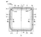
- FIG. 7 is a schematic plan view of a semiconductor device according to the fourth embodiment of the present invention.
- 8A and 8B are cross-sectional views of the semiconductor device, in which FIG. 8A is a cut surface taken along the cutting line VIIIa-VIIIa of FIG. 7, and FIG. 8B is a cutting line of FIG. The cut surfaces at VIIIb-VIIIb are shown respectively.
- 7 and 8 parts corresponding to those shown in FIGS. 1 to 6 are given the same reference numerals.
- the semiconductor device 71 is an example in which the features of the semiconductor devices according to the first, second, and third embodiments are combined. That is, in the contact hole 15 of the first embodiment, as in the second embodiment, a difference between the opening width W 1 and the opening width W 2 is provided, and the outer periphery of the active region 3 is surrounded so as to surround the termination structure 4. Are provided with a plurality of guard rings 5.
- this invention can also be implemented with another form.
- a configuration in which the conductivity type of each semiconductor portion of the semiconductor devices 1, 31, 61, 71 described above is reversed may be employed.
- the p-type portion may be n-type and the n-type portion may be p-type.
- the termination structure 4 may be omitted in the first embodiment and the second embodiment.
- the contact hole 15 for making contact between the termination structure 4 and the source electrode 14 does not need to be opened perpendicularly to the surface 21 of the SiC substrate 2, for example, a taper extending toward the surface of the interlayer film 12. You may open in the shape of a taper which narrows.
- the semiconductor employed in the semiconductor devices 1, 31, 61, 71 is not limited to SiC, but may be a semiconductor material having a plane orientation dependency with respect to dielectric breakdown strength, specifically, GaN, diamond, or the like. .
- an example in which the present invention is applied to a power MOSFET has been described.
- the present invention is not limited to an IGBT (Insulated). Gate Bipolar Transistor), JFET (Junction Field Effect) Transistor) and other structure semiconductor devices can be similarly applied.
Landscapes
- Electrodes Of Semiconductors (AREA)
Abstract
【課題】終端構造に対する局所的な電界集中を緩和することができる半導体装置を提供すること。 【解決手段】アクティブ領域3を有するn型SiC基板2と、アクティブ領域3の外周に沿って形成されたp型の終端構造4と、層間膜12を介してSiC基板2上に形成され、層間膜12を選択的に貫通して終端構造4に接続されたソース電極14とを含む半導体装置1において、終端構造4が、相対的に絶縁破壊強度が高い第二辺42と、第二辺42に比べて相対的に絶縁破壊強度が低い第一辺41とを形成し、第二辺42の形状と第一辺41の形状を、互いに非対称にする。
Description
本発明は、半導体装置に関する。
パワーエレクトロニクス分野では、高電圧が印加される高耐圧半導体装置(パワーデバイス)が用いられている。
たとえば、特許文献1は、n+ドレイン層上に積層されたnドリフト層と、nドリフト層の表面層に形成されたpベース領域と、pベース領域内に形成されたn+ソース領域と、pベース領域と重複して形成された高濃度のp+ウェル領域と、n+ソース領域とnドリフト層の表面露出部とに挟まれたpベース領域の表面上に、ゲート酸化膜を介して設けられたゲート電極層と、n+ソース領域とp+ウェル領域とに共通に接触するソース電極と、n+ドレイン層の裏面に設けられたドレイン電極と、ゲート電極層とソース電極とを絶縁する層間絶縁膜とを含む、SiC縦型MOSFETを開示している。
たとえば、特許文献1は、n+ドレイン層上に積層されたnドリフト層と、nドリフト層の表面層に形成されたpベース領域と、pベース領域内に形成されたn+ソース領域と、pベース領域と重複して形成された高濃度のp+ウェル領域と、n+ソース領域とnドリフト層の表面露出部とに挟まれたpベース領域の表面上に、ゲート酸化膜を介して設けられたゲート電極層と、n+ソース領域とp+ウェル領域とに共通に接触するソース電極と、n+ドレイン層の裏面に設けられたドレイン電極と、ゲート電極層とソース電極とを絶縁する層間絶縁膜とを含む、SiC縦型MOSFETを開示している。
本発明の第1の局面に係る半導体装置は、半導体素子が形成されたアクティブ領域を有する第1導電型の半導体層と、前記半導体層の表面部に前記アクティブ領域の外周に沿って形成された第2導電型の終端構造と、絶縁膜を介して前記半導体層上に形成され、前記絶縁膜を選択的に貫通して前記終端構造に接続された上部電極とを含み、前記終端構造は、相対的に絶縁破壊強度が高い高強度領域と、前記高強度領域に比べて相対的に絶縁破壊強度が低い低強度領域とを有し、前記高強度領域の形状と前記低強度領域の形状は、互いに非対称である(請求項1)。
この構成によれば、低強度領域の形状を電界が集中し難い形状にして、低強度領域の形状と高強度領域の形状を互いに非対称にすることによって、高電界状態時(たとえば、アバランシェ耐量試験等)における低強度領域の破壊を防止することができる。とりわけ、低強度領域および高強度領域にアバランシェ降伏が同時に発生するように、それぞれの形状を設計すれば、アバランシェ電流を各領域に均等に流すこともできる。
また、本発明の第2の局面に係る半導体装置は、半導体素子が形成されたアクティブ領域を有する第1導電型の半導体層と、前記半導体層の表面部に前記アクティブ領域の外周に沿って形成され、相対的に絶縁破壊強度が高い高強度領域と、前記高強度領域に比べて相対的に絶縁破壊強度が低い低強度領域とを有する第2導電型の終端構造と、絶縁膜を介して前記半導体層上に形成され、前記絶縁膜を選択的に貫通して前記高強度領域および前記低強度領域に接続された上部電極とを含み、前記高強度領域に対する前記上部電極の接触面積と、前記低強度領域に対する前記上部電極の接触面積は、互いに異なる(請求項2)。
相対的に絶縁破壊強度が低い低強度領域では、高強度領域に比べてアバランシェ電流が流れたときの電流密度が高くなり易い。そこで、本発明の構成によれば、低強度領域に対する上部電極の接触面積を大きくして、高強度領域に対する上部電極の接触面積と異ならせることによって、低強度領域に対する上部電極の接触抵抗を小さくすることができる。これにより、低強度領域における過剰発熱を防止し、熱破壊を防止することができる。その結果、アバランシェ耐量を向上させることができる。
相対的に絶縁破壊強度が低い低強度領域では、高強度領域に比べてアバランシェ電流が流れたときの電流密度が高くなり易い。そこで、本発明の構成によれば、低強度領域に対する上部電極の接触面積を大きくして、高強度領域に対する上部電極の接触面積と異ならせることによって、低強度領域に対する上部電極の接触抵抗を小さくすることができる。これにより、低強度領域における過剰発熱を防止し、熱破壊を防止することができる。その結果、アバランシェ耐量を向上させることができる。
前記第1および第2の局面に係る半導体装置では、前記半導体層は、絶縁破壊強度に関して面方位依存性を有する半導体材料からなっていてもよい(請求項3)。その場合、前記半導体材料は、SiC、GaNまたはダイヤモンドを含んでいてもよい(請求項4)。
本発明の第3の局面に係る半導体装置は、(0001)面に対して所定のオフ角θで傾斜した表面を有する第1導電型のSiCからなり、半導体素子が形成されたアクティブ領域を有する半導体層と、前記半導体層の前記表面部に前記アクティブ領域の外周に沿って四角環状に形成された第2導電型の終端構造と、絶縁膜を介して前記半導体層上に形成され、前記絶縁膜を選択的に貫通して前記終端構造に接続された上部電極とを含み、前記終端構造は、平面視において<11-20>方向で互いに向かい合う第一辺および第二辺を含み、断面視において、前記第一辺の外周端に対する接線は<11-20>方向を横切る方向に延び、前記第二辺の外周端に対する接線は<11-20>方向に沿う方向に延びるものであり、前記第一辺の長手方向両端部における角部の曲率半径は、前記第二辺の長手方向両端部の角部の曲率半径よりも大きい(請求項5)。
本発明の第3の局面に係る半導体装置は、(0001)面に対して所定のオフ角θで傾斜した表面を有する第1導電型のSiCからなり、半導体素子が形成されたアクティブ領域を有する半導体層と、前記半導体層の前記表面部に前記アクティブ領域の外周に沿って四角環状に形成された第2導電型の終端構造と、絶縁膜を介して前記半導体層上に形成され、前記絶縁膜を選択的に貫通して前記終端構造に接続された上部電極とを含み、前記終端構造は、平面視において<11-20>方向で互いに向かい合う第一辺および第二辺を含み、断面視において、前記第一辺の外周端に対する接線は<11-20>方向を横切る方向に延び、前記第二辺の外周端に対する接線は<11-20>方向に沿う方向に延びるものであり、前記第一辺の長手方向両端部における角部の曲率半径は、前記第二辺の長手方向両端部の角部の曲率半径よりも大きい(請求項5)。
SiCの絶縁破壊強度は、SiCの面方位に依存する。たとえば、<0001>方向と、<0001>方向に直交する<11-20>方向を比べると、<11-20>方向は、<0001>方向に比べて絶縁破壊強度が低い。そのため、同じ大きさの電界が加わる場合でも、その電界の方向が<0001>方向であればSiCが破壊され難く、一方、その電界の方向が<11-20>方向であれば、前者に比べてSiCが破壊され易い。
本発明の終端構造の第一辺および第二辺に関して、第一辺の外周端に対する接線は<11-20>方向を横切る方向に延び、第二辺の外周端に対する接線は<11-20>方向に沿う方向に延びている。各辺の外周端には、それぞれの接線と交差する方向に電界がかかることになる。つまり、第一辺の外周端には、接線と交差する方向(<11-20>方向に沿う方向)に電界がかかり、第二辺の外周端には、接線と交差する方向(<11-20>方向と交差する方向)に電界がかかる。したがって、<11-20>方向に沿う方向に電界がかかる第一辺は、<11-20>方向と交差する方向に電界がかかる第二辺に比べてSiCが破壊され易い。そのため、高電界状態時(たとえば、アバランシェ耐量試験等)に電界が集中しやすい第一辺および第二辺の各角部のうち、相対的に絶縁破壊強度が低い第一辺の角部が破壊するおそれがある。
そこで、本発明では、第一辺の長手方向両端部における角部の曲率半径が、第二辺の長手方向両端部の角部の曲率半径よりも大きいので、第一辺の角部への電界集中を緩和することができる。そのため、高電界状態時における第一辺の角部の破壊を防止することができる。とりわけ、第一辺の角部および第二辺の角部にアバランシェ降伏が同時に発生するように、それぞれの曲率半径を設計すれば、アバランシェ電流を第一辺および第二辺に均等に流すこともできる。
前記第3の局面に係る半導体装置では、前記上部電極は、前記第一辺および前記第二辺に接続されており、前記第一辺に対する前記上部電極の接触面積は、前記第二辺に対する前記上部電極の接触面積よりも大きいことが好ましい(請求項6)。
相対的に絶縁破壊強度が低い第一辺では、第二辺に比べてアバランシェ電流が流れたときの電流密度が高くなり易い。そこで、本発明の構成によれば、第一辺に対する上部電極の接触面積を大きくすることによって、第一辺に対する上部電極の接触抵抗を小さくすることができる。これにより、第一辺における過剰発熱を防止し、熱破壊を防止することができる。その結果、アバランシェ耐量を向上させることができる。
相対的に絶縁破壊強度が低い第一辺では、第二辺に比べてアバランシェ電流が流れたときの電流密度が高くなり易い。そこで、本発明の構成によれば、第一辺に対する上部電極の接触面積を大きくすることによって、第一辺に対する上部電極の接触抵抗を小さくすることができる。これにより、第一辺における過剰発熱を防止し、熱破壊を防止することができる。その結果、アバランシェ耐量を向上させることができる。
また、前記第3の局面に係る半導体装置では、前記上部電極は、前記第一辺および前記第二辺に接続されており、前記第一辺に対する前記上部電極の接触面積と、前記第二辺に対する前記上部電極の接触面積は、互いに等しくてもよい(請求項7)。
また、前記第3の局面に係る半導体装置は、前記終端構造に対して前記半導体層の外側に形成され、前記上部電極に対して電気的にフローティングされた複数の第2導電型のガードリングをさらに含む場合、前記複数のガードリングは、平面視において<11-20>方向で互いに向かい合い、前記第一辺に近いリング第一辺および前記第二辺に近いリング第二辺を含み、断面視において、前記リング第一辺の外周端に対する接線は<11-20>方向を横切る方向に延び、前記リング第二辺の外周端に対する接線は<11-20>方向に沿う方向に延びるものであり、前記リング第一辺のラインアンドスペースパターンのピッチは、前記リング第二辺のラインアンドスペースパターンのピッチよりも狭いことが好ましい(請求項8)。
また、前記第3の局面に係る半導体装置は、前記終端構造に対して前記半導体層の外側に形成され、前記上部電極に対して電気的にフローティングされた複数の第2導電型のガードリングをさらに含む場合、前記複数のガードリングは、平面視において<11-20>方向で互いに向かい合い、前記第一辺に近いリング第一辺および前記第二辺に近いリング第二辺を含み、断面視において、前記リング第一辺の外周端に対する接線は<11-20>方向を横切る方向に延び、前記リング第二辺の外周端に対する接線は<11-20>方向に沿う方向に延びるものであり、前記リング第一辺のラインアンドスペースパターンのピッチは、前記リング第二辺のラインアンドスペースパターンのピッチよりも狭いことが好ましい(請求項8)。
この構成によれば、複数のリング第一辺の群において、各リング第一辺と半導体層との接合によって発生する空乏層同士を連続的に繋げて広げることができるので、リング第一辺での電界を緩和することができる。
本発明の第4の局面に係る半導体装置は、(0001)面に対して所定のオフ角θで傾斜した表面を有する第1導電型のSiCからなり、半導体素子が形成されたアクティブ領域を有する半導体層と、前記半導体層の前記表面部に前記アクティブ領域の外周に沿って四角環状に形成され、平面視において<11-20>方向で互いに向かい合う第一辺および第二辺を含む第2導電型の終端構造と、絶縁膜を介して前記半導体層上に形成され、前記絶縁膜を選択的に貫通して前記第一辺および前記第二辺に接続された上部電極とを含み、断面視において、前記第一辺の外周端に対する接線は<11-20>方向を横切る方向に延び、前記第二辺の外周端に対する接線は<11-20>方向に沿う方向に延びるものであり、前記第一辺に対する前記上部電極の接触面積は、前記第二辺に対する前記上部電極の接触面積よりも大きい(請求項9)。
本発明の第4の局面に係る半導体装置は、(0001)面に対して所定のオフ角θで傾斜した表面を有する第1導電型のSiCからなり、半導体素子が形成されたアクティブ領域を有する半導体層と、前記半導体層の前記表面部に前記アクティブ領域の外周に沿って四角環状に形成され、平面視において<11-20>方向で互いに向かい合う第一辺および第二辺を含む第2導電型の終端構造と、絶縁膜を介して前記半導体層上に形成され、前記絶縁膜を選択的に貫通して前記第一辺および前記第二辺に接続された上部電極とを含み、断面視において、前記第一辺の外周端に対する接線は<11-20>方向を横切る方向に延び、前記第二辺の外周端に対する接線は<11-20>方向に沿う方向に延びるものであり、前記第一辺に対する前記上部電極の接触面積は、前記第二辺に対する前記上部電極の接触面積よりも大きい(請求項9)。
この構成によれば、第一辺に対する上部電極の接触面積を小さくすることによって、第一辺に対する上部電極の接触抵抗を小さくすることができる。これにより、第一辺における過剰発熱を防止し、熱破壊を防止することができる。その結果、アバランシェ耐量を向上させることができる。
本発明の第5の局面に係る半導体装置は、(0001)面に対して所定のオフ角θで傾斜した表面を有する第1導電型のSiCからなり、半導体素子が形成されたアクティブ領域を有する半導体層と、絶縁膜を介して前記半導体層上に形成された上部電極と、前記半導体層の前記表面部に前記アクティブ領域の外周に沿って四角環状に形成され、前記上部電極に対して電気的にフローティングされた複数の第2導電型のガードリングとを含み、前記複数のガードリングは、平面視において<11-20>方向で互いに向かい合うリング第一辺およびリング第二辺を含み、断面視において、前記リング第一辺の外周端に対する接線は<11-20>方向を横切る方向に延び、前記リング第二辺の外周端に対する接線は<11-20>方向に沿う方向に延びるものであり、前記リング第一辺のラインアンドスペースパターンのピッチは、前記リング第二辺のラインアンドスペースパターンのピッチよりも狭い(請求項10)。
本発明の第5の局面に係る半導体装置は、(0001)面に対して所定のオフ角θで傾斜した表面を有する第1導電型のSiCからなり、半導体素子が形成されたアクティブ領域を有する半導体層と、絶縁膜を介して前記半導体層上に形成された上部電極と、前記半導体層の前記表面部に前記アクティブ領域の外周に沿って四角環状に形成され、前記上部電極に対して電気的にフローティングされた複数の第2導電型のガードリングとを含み、前記複数のガードリングは、平面視において<11-20>方向で互いに向かい合うリング第一辺およびリング第二辺を含み、断面視において、前記リング第一辺の外周端に対する接線は<11-20>方向を横切る方向に延び、前記リング第二辺の外周端に対する接線は<11-20>方向に沿う方向に延びるものであり、前記リング第一辺のラインアンドスペースパターンのピッチは、前記リング第二辺のラインアンドスペースパターンのピッチよりも狭い(請求項10)。
この構成によれば、複数のリング第一辺の群において、各リング第一辺と半導体層との接合によって発生する空乏層同士を連続的に繋げて広げることができるので、リング第一辺での電界を緩和することができる。
以下では、本発明の実施の形態を、添付図面を参照して詳細に説明する。
図1は、本発明の第1実施形態に係る半導体装置の模式的な平面図である。
半導体装置1は、SiC(炭化シリコン)を用いたパワーMOSFET(Metal-Oxide-Semiconductor
Field Effect Transistor)素子(個別素子)を含み、たとえば、図1の紙
面における上下方向の長さは1mm程度である。
図1は、本発明の第1実施形態に係る半導体装置の模式的な平面図である。
半導体装置1は、SiC(炭化シリコン)を用いたパワーMOSFET(Metal-Oxide-Semiconductor
Field Effect Transistor)素子(個別素子)を含み、たとえば、図1の紙
面における上下方向の長さは1mm程度である。
半導体装置1は、半導体層の一例としてのSiC基板2上の中央部に配置され、電界効果トランジスタとして機能するアクティブ領域3を備えている。このアクティブ領域3の周縁部には、その外周に沿って四角環状の終端構造4が形成されている。
図2(a)(b)は、前記半導体装置の断面図であって、図2(a)は図1の切断線IIa-IIaでの切断面、図2(b)は図1の切断線IIb-IIbでの切断面をそれぞれ示す。
図2(a)(b)は、前記半導体装置の断面図であって、図2(a)は図1の切断線IIa-IIaでの切断面、図2(b)は図1の切断線IIb-IIbでの切断面をそれぞれ示す。
半導体装置1は、いわゆるDMOS(Double-Diffusion
Metal-Oxide-Semiconductor)構造を有している。ただし、SiCプロセスでは、二重拡散技術を応用することはできず、二重イオン注入(Double-Implantation)によってDMOS構造のデバイスが作製される。
SiC基板2は、この実施形態では、n型であり、電界効果トランジスタのドレイン領域として機能する。ここで、SiC基板2について具体的に説明する。
Metal-Oxide-Semiconductor)構造を有している。ただし、SiCプロセスでは、二重拡散技術を応用することはできず、二重イオン注入(Double-Implantation)によってDMOS構造のデバイスが作製される。
SiC基板2は、この実施形態では、n型であり、電界効果トランジスタのドレイン領域として機能する。ここで、SiC基板2について具体的に説明する。
SiC基板2を構成するSiCは、同一の組成で様々な積層構造をとる結晶多形(ポリタイプ)を示す材料であり、数100種類以上のポリタイプが存在する。この実施形態では、SiC基板2は、4H-SiCであるが、これに限らず、たとえば、3C-SiC、2H-SiC、6H-SiC、15R-SiCなどであってもよい。これらの中では、6H-SiCなどの六方晶SiCが好ましい。
4H-SiCの結晶構造は、六方晶系で近似することができ、1つのシリコン原子に対して4つの炭素原子が結合している。4つの炭素原子は、シリコン原子を中央に配置した正四面体の4つの頂点に位置している。これらの4つの炭素原子は、1つのシリコン原子が炭素原子に対して<0001>方向に位置し、他の3つの炭素原子がシリコン原子に対して<000-1>方向に位置している。<0001>方向および<000-1>方向は六角柱の軸方向に沿い、この<0001>方向を法線とする面(六角柱の頂面)が(0001)面(Si面)である。一方、<000-1>方向を法線とする面(六角柱の下面)が(000-1)面(C面)である。
そして、この実施形態では、SiC基板2は、所定のオフ角θを有している。具体的には、SiC基板2の主面(表面21)が、(0001)面に対して<11-20>方向に角度θで傾斜した面となっている。すなわち、SiC基板2の表面21は、その法線nの方向が<0001>方向と一致しておらず、(0001)面に対して<11-20>方向(オフ方向)にオフ角θで傾斜している。オフ方向とは、<0001>方向に対するSiC基板2の法線nの傾斜する方向を指し、<0001>方向から法線nを(0001)面に投影(射影)したベクトルの向きで示されるものである。すなわち、この実施形態では、法線nの投影ベクトルの向きが、<11-20>方向に一致している。
これにより、SiC基板2は、(0001)面から構成される平坦なテラス面23と、表面21が(0001)面に対して傾斜すること(オフ角θ)により生じるテラス面23の段差部分とから形成され、段差部分は<11-20>方向に垂直な(11-20)面であるステップ面(図示せず)を有している。
このSiC基板2の表面21側には、複数のp型ウェル6が格子配列されて多数形成されていて、アクティブ領域3を形成している。また、SiC基板2の裏面22には、たとえば、ニッケル金属膜からなるドレイン電極7が形成されている。
このSiC基板2の表面21側には、複数のp型ウェル6が格子配列されて多数形成されていて、アクティブ領域3を形成している。また、SiC基板2の裏面22には、たとえば、ニッケル金属膜からなるドレイン電極7が形成されている。
個々のp型ウェル6内には、n+型ソース領域8と、このn+型ソース領域8に取り囲まれたp+型ウェルコンタクト領域9とが形成されている。そして、隣接するp型ウェル6に跨るようにゲート電極10が形成されており、このゲート電極10とSiC基板2との間にゲート絶縁膜11が介在されている。ゲート電極10は、n+型ソース領域8とドレイン領域としてのSiC基板2(p型ウェル6の間の領域)との間に跨っていて、p型ウェル6の表面における反転層(チャネル)の形成を制御する。
さらに、ゲート電極10を覆うように、たとえば酸化シリコンからなる絶縁膜の一例としての層間膜12が形成されている。この層間膜12は、さらにアクティブ領域3からその周囲の領域をも覆っている。層間膜12には、p型ウェル6の中央領域にコンタクトホール13が選択的に形成されている。このコンタクトホール13は、p+型ウェルコンタクト領域9およびその周囲のn+型ソース領域8の一部を露出させることができる領域に形成されている。コンタクトホール13に入り込むように、基板上の大部分を覆う上部電極の一例としてのソース電極14(たとえばアルミニウムからなるもの)が形成されている。したがって、n+型ソース領域8は、ソース電極14と同電位となる。また、p型ウェル6は、p+型ウェルコンタクト領域9を介してソース電極14に接続されるので、このソース電極14と同電位となる。
前述のように、アクティブ領域3の周縁部には、p型不純物を導入して形成された終端構造4が形成されている。この終端構造4は、アクティブ領域3の全周に渡って形成されている。そして、層間膜12には、終端構造4に対応するコンタクトホール15が形成されている。コンタクトホール15は、終端構造4の全周に渡って一定幅(開口幅が全周に渡って一定)の四角環状に形成されている。終端構造4には、コンタクトホール15に露出する部分(後述する第一辺41~第四辺44全て)において、ソース電極14が接している。これにより、終端構造4は、ソース電位(たとえば0V)に固定されることになる。終端構造4をソースと同電位に固定することで、アクティブ領域3の周囲領域における電界分布を均一化および安定化することができる。さらに、p型ウェル6から広がる空乏層16(二点鎖線)を、終端構造4を超えて広げることができる。
終端構造4は、図1に示すように、平面視において<11-20>方向で互いに向かい合う低強度領域の一例としての第一辺41および高強度領域の一例としての第二辺42、および<11-20>方向に直交する方向で互いに向かい合う第三辺43および第四辺44を含む。
この実施形態では、SiC基板2がオフ角θを有するオフ基板である。そのため、<11-20>方向に対する、第一辺41の外周端の接線41Lおよび第二辺42の外周端の接線42Lそれぞれの関係が互いに異なっている。具体的には、図2に示すように、断面視において、第一辺41の接線41Lが<11-20>方向を横切る方向に延びているのに対し、第二辺42の接線42Lは、<11-20>方向に沿う方向(この実施形態では、<11-20>方向に平行)に延びている。なお、接線41Lおよび接線42Lは、たとえば、SiC基板2の表面21に対してオフ角θで傾斜した直線を、表面21に沿って平行移動させることによって描くことができる。
この実施形態では、SiC基板2がオフ角θを有するオフ基板である。そのため、<11-20>方向に対する、第一辺41の外周端の接線41Lおよび第二辺42の外周端の接線42Lそれぞれの関係が互いに異なっている。具体的には、図2に示すように、断面視において、第一辺41の接線41Lが<11-20>方向を横切る方向に延びているのに対し、第二辺42の接線42Lは、<11-20>方向に沿う方向(この実施形態では、<11-20>方向に平行)に延びている。なお、接線41Lおよび接線42Lは、たとえば、SiC基板2の表面21に対してオフ角θで傾斜した直線を、表面21に沿って平行移動させることによって描くことができる。
また、終端構造4では、第一辺41の長手方向両端部における角部41Cの曲率半径R1は、第二辺42の長手方向両端部の角部42Cの曲率半径R2よりも大きくなっている。角部41Cおよび42Cは、それぞれ第一辺41および第二辺42が、第三辺43および第四辺44と交わってできる部分である。好ましくは、曲率半径R1は、60μm~100μmであり、曲率半径R2は、20μm~100μmである。曲率半径R1>曲率半径R2であることによって、第一辺41の形状と第二辺42の形状は、第三辺43および第四辺44の中心を通る対称軸aに対して互いに非対称の関係になっている。
また、この実施形態で半導体基板として用いられたSiCの絶縁破壊強度は、SiCの面方位に依存する。たとえば、<0001>方向と<11-20>方向を比べると、<11-20>方向は、<0001>方向に比べて絶縁破壊強度が低い。そのため、同じ大きさの電界が加わる場合でも、その電界の方向が<0001>方向であればSiCが破壊され難く、一方、その電界の方向が<11-20>方向であれば、前者に比べてSiCが破壊され易い。
前述のように、この実施形態では、断面視において、第一辺41の接線41Lが<11-20>方向を横切る方向に延びているのに対し、第二辺42の接線42Lは、<11-20>方向に沿う方向(この実施形態では、<11-20>方向に平行)に延びている。一方、第一辺41および第二辺42の各外周端には、それぞれの接線41L,42Lと交差する方向に電界がかかることになる。つまり、第一辺41の外周端には、接線41Lと交差する方向(<11-20>方向に沿う方向)に電界がかかり、第二辺42の外周端には、接線42Lと交差する方向(<11-20>方向と交差する方向)に電界がかかる。したがって、<11-20>方向に沿う方向に電界がかかる第一辺41は、<11-20>方向と交差する方向に電界がかかる第二辺42に比べてSiCが破壊され易い。そのため、高電界状態時(たとえば、アバランシェ耐量試験等)に電界が集中しやすい第一辺41および第二辺42の各角部41C,42Cのうち、相対的に絶縁破壊強度が低い第一辺41の角部41Cが破壊するおそれがある。
そこで、この実施形態では、第一辺41の長手方向両端部における角部41Cの曲率半径R1が、第二辺42の長手方向両端部の角部42Cの曲率半径R2よりも大きくなっている。これにより、第一辺41の角部41Cへの電界集中を緩和することができる。そのため、高電界状態時における第一辺41の角部41Cの破壊を防止することができる。とりわけ、第一辺41の角部41Cおよび第二辺42の角部42Cにアバランシェ降伏が同時に発生するように、それぞれの曲率半径R1,R2を設計すれば、アバランシェ電流を第一辺41および第二辺42に均等に流すこともできる。
図3は、本発明の第2実施形態に係る半導体装置の模式的な平面図である。図4(a)(b)は、前記半導体装置の断面図であって、図4(a)は図3の切断線IVa-IVaでの切断面、図4(b)は図3の切断線IVb-IVbでの切断面をそれぞれ示す。図3および図4において、前述の図1および図2に示された各部と対応する部分には同一の参照符号を付して示す。
この半導体装置31では、終端構造4において、第一辺41の角部41Cの曲率半径R1が、第二辺42の角部42Cの曲率半径R2と同じである。すなわち、第一辺41の形状と第二辺42の形状が、対称軸aに対して互いに線対称の関係になっている。
一方、コンタクトホール15の開口幅が一定ではない。具体的には、第一辺41を露出させる部分の開口幅W1と、第二辺42を露出させる部分の開口幅W2とが、互いに異なっている。具体的には、開口幅W1が開口幅W2よりも広くなっている。これにより、半導体装置31では、第一辺41に対するソース電極14の接触面積が、第二辺42に対するソース電極14の接触面積よりも大きくなっている。
一方、コンタクトホール15の開口幅が一定ではない。具体的には、第一辺41を露出させる部分の開口幅W1と、第二辺42を露出させる部分の開口幅W2とが、互いに異なっている。具体的には、開口幅W1が開口幅W2よりも広くなっている。これにより、半導体装置31では、第一辺41に対するソース電極14の接触面積が、第二辺42に対するソース電極14の接触面積よりも大きくなっている。
前述のように、面内で絶縁破壊強度が互いに異なる領域が存在するSiC基板2では、相対的に絶縁破壊強度が低い第一辺41において、第二辺42に比べてアバランシェ電流が流れたときの電流密度が高くなり易い。
そこで、この実施形態の構成によれば、第一辺41に対するソース電極14の接触面積を小さくすることによって、第一辺41に対するソース電極14の接触抵抗を小さくすることができる。これにより、第一辺41における過剰発熱を防止し、熱破壊を防止することができる。その結果、アバランシェ耐量を向上させることができる。
そこで、この実施形態の構成によれば、第一辺41に対するソース電極14の接触面積を小さくすることによって、第一辺41に対するソース電極14の接触抵抗を小さくすることができる。これにより、第一辺41における過剰発熱を防止し、熱破壊を防止することができる。その結果、アバランシェ耐量を向上させることができる。
図5は、本発明の第3実施形態に係る半導体装置の模式的な平面図である。図6(a)(b)は、前記半導体装置の断面図であって、図6(a)は図5の切断線VIa-VIaでの切断面、図6(b)は図5の切断線VIb-VIbでの切断面をそれぞれ示す。図5および図6において、前述の図1および図2に示された各部と対応する部分には同一の参照符号を付して示す。
この半導体装置61では、終端構造4において、第一辺41の角部41Cの曲率半径R1が、第二辺42の角部42Cの曲率半径R2と同じである。すなわち、第一辺41の形状と第二辺42の形状が、対称軸aに対して互いに線対称の関係になっている。
また、終端構造4を取り囲むように、アクティブ領域3の外周に沿って複数のガードリング5が形成されている。複数のガードリング5は、終端構造4と相似形に形成されており、終端構造4との間に一定の間隔を隔てたSiC基板2の外側に配置されている。終端構造4とガードリング5との間隔は、全周にわたって至るところでほぼ一定である。なお、図5では図解し易くするために、複数のガードリング5を2本しか表していないが、複数のガードリング5は、3本、4本もしくはそれ以上(図6では、5本のガードリング5を表している)であってもよい。
また、終端構造4を取り囲むように、アクティブ領域3の外周に沿って複数のガードリング5が形成されている。複数のガードリング5は、終端構造4と相似形に形成されており、終端構造4との間に一定の間隔を隔てたSiC基板2の外側に配置されている。終端構造4とガードリング5との間隔は、全周にわたって至るところでほぼ一定である。なお、図5では図解し易くするために、複数のガードリング5を2本しか表していないが、複数のガードリング5は、3本、4本もしくはそれ以上(図6では、5本のガードリング5を表している)であってもよい。
複数のガードリング5は、アクティブ領域3の周囲におけるSiC基板2の表面21に、終端構造4から一定の間隔を開けた領域にp型不純物を導入して形成されている。複数のガードリング5は、SiC基板2の表面21を覆う層間膜12によって覆われており、電気的に浮遊状態に保持されるようになっている。なお、ソース電極14は、図6に示すように、層間膜12を介して複数のガードリング5に選択的に対向していてもよいし、全てのガードリング5に対向していてもよい。また、ソース電極14は、その周縁部がガードリング5と終端構造4との間に配置されることによって、ガードリング5と対向していなくてもよい。
個々のガードリング5は、図5に示すように、平面視において<11-20>方向で互いに向かい合うリング第一辺51およびリング第二辺52、および<11-20>方向に直交する方向で互いに向かい合うリング第三辺53およびリング第四辺54を含む。
また、ガードリング5についても終端構造4と同様に、<11-20>方向に対する、リング第一辺51の外周端の接線51Lおよびリング第二辺52の外周端の接線52Lそれぞれの関係が互いに異なっている。具体的には、図6に示すように、断面視において、リング第一辺51の接線51Lが<11-20>方向を横切る方向に延びているのに対し、リング第二辺52の接線52Lは、<11-20>方向に沿う方向(この実施形態では、<11-20>方向に平行)に延びている。なお、接線51Lおよび接線52Lは、たとえば、SiC基板2の表面21に対してオフ角θで傾斜した直線を、表面21に沿って平行移動させることによって描くことができる。
また、ガードリング5についても終端構造4と同様に、<11-20>方向に対する、リング第一辺51の外周端の接線51Lおよびリング第二辺52の外周端の接線52Lそれぞれの関係が互いに異なっている。具体的には、図6に示すように、断面視において、リング第一辺51の接線51Lが<11-20>方向を横切る方向に延びているのに対し、リング第二辺52の接線52Lは、<11-20>方向に沿う方向(この実施形態では、<11-20>方向に平行)に延びている。なお、接線51Lおよび接線52Lは、たとえば、SiC基板2の表面21に対してオフ角θで傾斜した直線を、表面21に沿って平行移動させることによって描くことができる。
また、複数のガードリング5では、リング第一辺51のラインアンドスペースパターンのピッチが、リング第二辺52のラインアンドスペースパターンのピッチよりも狭くなっている。具体的には、ガードリング5の幅と、当該ガードリング5に隣り合うガードリング5との間隔との合計幅を単位幅Wとしたとき、単位幅Wに対するリング第一辺51の占有率が、単位幅Wに対するリング第二辺52の占有率よりも大きくなっている。好ましくは、リング第一辺51の占有率は、60~80%であり、リング第二辺52の占有率は、20~40%である。
このような構成によれば、終端構造4をソースと同電位に固定することで、アクティブ領域3の周囲領域における電界分布を均一化および安定化することができる。さらに、p型ウェル6から広がる空乏層16(二点鎖線)は、終端構造4を超え、空乏層17(実線)に繋がってSiC基板2の端面に向かって延びることとなる。これにより、電界の集中をさらに効果的に緩和することができる。
さらに、この実施形態では、複数のガードリング5において、リング第一辺51のラインアンドスペースパターンのピッチが、リング第二辺52のラインアンドスペースパターンのピッチよりも狭くなっている。
そのため、リング第一辺51の群において、各リング第一辺51とSiC基板2との接合によって発生する空乏層17同士を連続的に繋げて広げることができるので、リング第一辺51での電界を一層緩和することができる。
そのため、リング第一辺51の群において、各リング第一辺51とSiC基板2との接合によって発生する空乏層17同士を連続的に繋げて広げることができるので、リング第一辺51での電界を一層緩和することができる。
図7は、本発明の第4実施形態に係る半導体装置の模式的な平面図である。図8(a)(b)は、前記半導体装置の断面図であって、図8(a)は図7の切断線VIIIa-VIIIaでの切断面、図8(b)は図7の切断線VIIIb-VIIIbでの切断面をそれぞれ示す。図7および図8において、前述の図1~図6に示された各部と対応する部分には同一の参照符号を付して示す。
この半導体装置71は、前述の第1、第2および第3実施形態に係る半導体装置の特徴を組み合わせた例である。すなわち、第1実施形態のコンタクトホール15において、第2実施形態と同様に、開口幅W1と開口幅W2との差を設け、さらに、終端構造4を取り囲むように、アクティブ領域3の外周に沿って複数のガードリング5を設けたものである。
以上、本発明の実施形態について説明したが、本発明は、さらに他の形態で実施することも可能である。
たとえば、前述の半導体装置1,31,61,71の各半導体部分の導電型を反転した構成が採用されてもよい。たとえば、半導体装置1において、p型の部分がn型であり、n型の部分がp型であってもよい。
たとえば、前述の半導体装置1,31,61,71の各半導体部分の導電型を反転した構成が採用されてもよい。たとえば、半導体装置1において、p型の部分がn型であり、n型の部分がp型であってもよい。
また、前述の実施形態の開示から把握される特徴は、異なる実施形態間でも互いに組み合わせることができる。また、各実施形態において表した構成要素は、本発明の範囲で組み合わせることができる。たとえば、第1の実施形態および第2の実施形態において、終端構造4を省略してもよい。
また、終端構造4とソース電極14とのコンタクトをとるためのコンタクトホール15は、SiC基板2の表面21に対して垂直に開口する必要はなく、たとえば、層間膜12の表面に向かって広がるテーパ状、もしくは狭まるテーパ状に開口してもよい。
また、終端構造4とソース電極14とのコンタクトをとるためのコンタクトホール15は、SiC基板2の表面21に対して垂直に開口する必要はなく、たとえば、層間膜12の表面に向かって広がるテーパ状、もしくは狭まるテーパ状に開口してもよい。
また、半導体装置1,31,61,71に採用される半導体は、SiCに限らず、絶縁破壊強度に関して面方位依存性を有する半導体材料、具体的には、GaN、ダイヤモンド等であってもよい。
また、前述の実施形態では、本発明をパワーMOSFETに適用した例について説明したが、本発明は、IGBT(Insulated
Gate Bipolar Transistor)、JFET(Junction Field Effect
Transistor)、その他の構造の半導体デバイスにも同様に適用することができる。
また、前述の実施形態では、本発明をパワーMOSFETに適用した例について説明したが、本発明は、IGBT(Insulated
Gate Bipolar Transistor)、JFET(Junction Field Effect
Transistor)、その他の構造の半導体デバイスにも同様に適用することができる。
その他、特許請求の範囲に記載された事項の範囲で種々の設計変更を施すことが可能である。
1 半導体装置
2 SiC基板
21 表面
3 アクティブ領域
4 終端構造
41 第一辺
41C 角部
41L 接線
42 第二辺
42C 角部
42L 接線
5 ガードリング
51 リング第一辺
51L 接線
52 リング第二辺
52L 接線
12 層間膜
14 ソース電極
31 半導体装置
61 半導体装置
71 半導体装置
2 SiC基板
21 表面
3 アクティブ領域
4 終端構造
41 第一辺
41C 角部
41L 接線
42 第二辺
42C 角部
42L 接線
5 ガードリング
51 リング第一辺
51L 接線
52 リング第二辺
52L 接線
12 層間膜
14 ソース電極
31 半導体装置
61 半導体装置
71 半導体装置
Claims (10)
- 半導体素子が形成されたアクティブ領域を有する第1導電型の半導体層と、
前記半導体層の表面部に前記アクティブ領域の外周に沿って形成された第2導電型の終端構造と、
絶縁膜を介して前記半導体層上に形成され、前記絶縁膜を選択的に貫通して前記終端構造に接続された上部電極とを含み、
前記終端構造は、相対的に絶縁破壊強度が高い高強度領域と、前記高強度領域に比べて相対的に絶縁破壊強度が低い低強度領域とを有し、
前記高強度領域の形状と前記低強度領域の形状は、互いに非対称である、半導体装置。 - 半導体素子が形成されたアクティブ領域を有する第1導電型の半導体層と、
前記半導体層の表面部に前記アクティブ領域の外周に沿って形成され、相対的に絶縁破壊強度が高い高強度領域と、前記高強度領域に比べて相対的に絶縁破壊強度が低い低強度領域とを有する第2導電型の終端構造と、
絶縁膜を介して前記半導体層上に形成され、前記絶縁膜を選択的に貫通して前記高強度領域および前記低強度領域に接続された上部電極とを含み、
前記高強度領域に対する前記上部電極の接触面積と、前記低強度領域に対する前記上部電極の接触面積は、互いに異なる、半導体装置。 - 前記半導体層は、絶縁破壊強度に関して面方位依存性を有する半導体材料からなる、請求項1または2に記載の半導体装置。
- 前記半導体材料は、SiC、GaNまたはダイヤモンドを含む、請求項3に記載の半導体装置。
- (0001)面に対して所定のオフ角θで傾斜した表面を有する第1導電型のSiCからなり、半導体素子が形成されたアクティブ領域を有する半導体層と、
前記半導体層の前記表面部に前記アクティブ領域の外周に沿って四角環状に形成された第2導電型の終端構造と、
絶縁膜を介して前記半導体層上に形成され、前記絶縁膜を選択的に貫通して前記終端構造に接続された上部電極とを含み、
前記終端構造は、平面視において<11-20>方向で互いに向かい合う第一辺および第二辺を含み、断面視において、前記第一辺の外周端に対する接線は<11-20>方向を横切る方向に延び、前記第二辺の外周端に対する接線は<11-20>方向に沿う方向に延びるものであり、
前記第一辺の長手方向両端部における角部の曲率半径は、前記第二辺の長手方向両端部の角部の曲率半径よりも大きい、半導体装置。 - 前記上部電極は、前記第一辺および前記第二辺に接続されており、
前記第一辺に対する前記上部電極の接触面積は、前記第二辺に対する前記上部電極の接触面積よりも大きい、請求項5に記載の半導体装置。 - 前記上部電極は、前記第一辺および前記第二辺に接続されており、
前記第一辺に対する前記上部電極の接触面積と、前記第二辺に対する前記上部電極の接触面積は、互いに等しい、請求項5に記載の半導体装置。 - 前記半導体装置は、前記終端構造に対して前記半導体層の外側に形成され、前記上部電極に対して電気的にフローティングされた複数の第2導電型のガードリングをさらに含み、
前記複数のガードリングは、平面視において<11-20>方向で互いに向かい合い、前記第一辺に近いリング第一辺および前記第二辺に近いリング第二辺を含み、断面視において、前記リング第一辺の外周端に対する接線は<11-20>方向を横切る方向に延び、前記リング第二辺の外周端に対する接線は<11-20>方向に沿う方向に延びるものであり、
前記リング第一辺のラインアンドスペースパターンのピッチは、前記リング第二辺のラインアンドスペースパターンのピッチよりも狭い、請求項5~7のいずれか一項に記載の半導体装置。 - (0001)面に対して所定のオフ角θで傾斜した表面を有する第1導電型のSiCからなり、半導体素子が形成されたアクティブ領域を有する半導体層と、
前記半導体層の前記表面部に前記アクティブ領域の外周に沿って四角環状に形成され、平面視において<11-20>方向で互いに向かい合う第一辺および第二辺を含む第2導電型の終端構造と、
絶縁膜を介して前記半導体層上に形成され、前記絶縁膜を選択的に貫通して前記第一辺および前記第二辺に接続された上部電極とを含み、
断面視において、前記第一辺の外周端に対する接線は<11-20>方向を横切る方向に延び、前記第二辺の外周端に対する接線は<11-20>方向に沿う方向に延びるものであり、
前記第一辺に対する前記上部電極の接触面積は、前記第二辺に対する前記上部電極の接触面積よりも大きい、半導体装置。 - (0001)面に対して所定のオフ角θで傾斜した表面を有する第1導電型のSiCからなり、半導体素子が形成されたアクティブ領域を有する半導体層と、
絶縁膜を介して前記半導体層上に形成された上部電極と、
前記半導体層の前記表面部に前記アクティブ領域の外周に沿って四角環状に形成され、前記上部電極に対して電気的にフローティングされた複数の第2導電型のガードリングとを含み、
前記複数のガードリングは、平面視において<11-20>方向で互いに向かい合うリング第一辺およびリング第二辺を含み、断面視において、前記リング第一辺の外周端に対する接線は<11-20>方向を横切る方向に延び、前記リング第二辺の外周端に対する接線は<11-20>方向に沿う方向に延びるものであり、
前記リング第一辺のラインアンドスペースパターンのピッチは、前記リング第二辺のラインアンドスペースパターンのピッチよりも狭い、半導体装置。
Priority Applications (1)
| Application Number | Priority Date | Filing Date | Title |
|---|---|---|---|
| US14/398,334 US9337257B2 (en) | 2012-05-11 | 2013-05-10 | Semiconductor device |
Applications Claiming Priority (2)
| Application Number | Priority Date | Filing Date | Title |
|---|---|---|---|
| JP2012109949A JP2013239488A (ja) | 2012-05-11 | 2012-05-11 | 半導体装置 |
| JP2012-109949 | 2012-05-11 |
Publications (1)
| Publication Number | Publication Date |
|---|---|
| WO2013168795A1 true WO2013168795A1 (ja) | 2013-11-14 |
Family
ID=49550827
Family Applications (1)
| Application Number | Title | Priority Date | Filing Date |
|---|---|---|---|
| PCT/JP2013/063157 Ceased WO2013168795A1 (ja) | 2012-05-11 | 2013-05-10 | 半導体装置 |
Country Status (3)
| Country | Link |
|---|---|
| US (1) | US9337257B2 (ja) |
| JP (1) | JP2013239488A (ja) |
| WO (1) | WO2013168795A1 (ja) |
Cited By (1)
| Publication number | Priority date | Publication date | Assignee | Title |
|---|---|---|---|---|
| CN107949917A (zh) * | 2015-09-24 | 2018-04-20 | 住友电气工业株式会社 | 碳化硅半导体器件及其制造方法 |
Families Citing this family (4)
| Publication number | Priority date | Publication date | Assignee | Title |
|---|---|---|---|---|
| WO2015145593A1 (ja) * | 2014-03-26 | 2015-10-01 | 株式会社日立製作所 | 半導体装置及びその製造方法,パワーモジュール,電力変換装置,3相モータシステム,自動車並びに鉄道車両 |
| US9806186B2 (en) * | 2015-10-02 | 2017-10-31 | D3 Semiconductor LLC | Termination region architecture for vertical power transistors |
| EP3401954B1 (en) * | 2016-01-05 | 2020-05-06 | Hitachi, Ltd. | Semiconductor device |
| KR102150520B1 (ko) * | 2019-06-21 | 2020-09-01 | 주식회사 티씨케이 | Cvd 방식으로 형성된 sic 구조체 |
Citations (7)
| Publication number | Priority date | Publication date | Assignee | Title |
|---|---|---|---|---|
| JPS6338259A (ja) * | 1986-08-01 | 1988-02-18 | Fujitsu Ltd | 半導体装置 |
| JP2004158817A (ja) * | 2002-09-09 | 2004-06-03 | Toyota Central Res & Dev Lab Inc | 半導体装置 |
| JP2006100593A (ja) * | 2004-09-29 | 2006-04-13 | Toshiba Corp | 高耐圧半導体装置 |
| JP2007081144A (ja) * | 2005-09-14 | 2007-03-29 | Mitsubishi Electric Corp | 炭化ケイ素半導体装置 |
| JP2009206223A (ja) * | 2008-02-27 | 2009-09-10 | New Japan Radio Co Ltd | 半導体装置 |
| JP2010212331A (ja) * | 2009-03-09 | 2010-09-24 | Nissan Motor Co Ltd | 半導体装置 |
| JP2010219365A (ja) * | 2009-03-18 | 2010-09-30 | New Japan Radio Co Ltd | 半導体装置およびその製造方法 |
Family Cites Families (6)
| Publication number | Priority date | Publication date | Assignee | Title |
|---|---|---|---|---|
| US5404040A (en) * | 1990-12-21 | 1995-04-04 | Siliconix Incorporated | Structure and fabrication of power MOSFETs, including termination structures |
| JP3460585B2 (ja) | 1998-07-07 | 2003-10-27 | 富士電機株式会社 | 炭化けい素mos半導体素子の製造方法 |
| JP4972293B2 (ja) | 2005-06-09 | 2012-07-11 | ローム株式会社 | 半導体装置およびその製造方法 |
| JP4921880B2 (ja) | 2006-07-28 | 2012-04-25 | 株式会社東芝 | 高耐圧半導体装置 |
| US8614482B2 (en) * | 2011-12-30 | 2013-12-24 | Force Mos Technology Co., Ltd. | Semiconductor power device having improved termination structure for mask saving |
| US9219044B2 (en) * | 2013-11-18 | 2015-12-22 | Applied Materials, Inc. | Patterned photoresist to attach a carrier wafer to a silicon device wafer |
-
2012
- 2012-05-11 JP JP2012109949A patent/JP2013239488A/ja active Pending
-
2013
- 2013-05-10 US US14/398,334 patent/US9337257B2/en active Active
- 2013-05-10 WO PCT/JP2013/063157 patent/WO2013168795A1/ja not_active Ceased
Patent Citations (7)
| Publication number | Priority date | Publication date | Assignee | Title |
|---|---|---|---|---|
| JPS6338259A (ja) * | 1986-08-01 | 1988-02-18 | Fujitsu Ltd | 半導体装置 |
| JP2004158817A (ja) * | 2002-09-09 | 2004-06-03 | Toyota Central Res & Dev Lab Inc | 半導体装置 |
| JP2006100593A (ja) * | 2004-09-29 | 2006-04-13 | Toshiba Corp | 高耐圧半導体装置 |
| JP2007081144A (ja) * | 2005-09-14 | 2007-03-29 | Mitsubishi Electric Corp | 炭化ケイ素半導体装置 |
| JP2009206223A (ja) * | 2008-02-27 | 2009-09-10 | New Japan Radio Co Ltd | 半導体装置 |
| JP2010212331A (ja) * | 2009-03-09 | 2010-09-24 | Nissan Motor Co Ltd | 半導体装置 |
| JP2010219365A (ja) * | 2009-03-18 | 2010-09-30 | New Japan Radio Co Ltd | 半導体装置およびその製造方法 |
Cited By (1)
| Publication number | Priority date | Publication date | Assignee | Title |
|---|---|---|---|---|
| CN107949917A (zh) * | 2015-09-24 | 2018-04-20 | 住友电气工业株式会社 | 碳化硅半导体器件及其制造方法 |
Also Published As
| Publication number | Publication date |
|---|---|
| JP2013239488A (ja) | 2013-11-28 |
| US20150333120A1 (en) | 2015-11-19 |
| US9337257B2 (en) | 2016-05-10 |
Similar Documents
| Publication | Publication Date | Title |
|---|---|---|
| JP5896554B2 (ja) | 半導体装置 | |
| JP4839519B2 (ja) | 半導体装置 | |
| US8648349B2 (en) | Semiconductor device | |
| JP5718627B2 (ja) | 半導体装置 | |
| JP5939127B2 (ja) | 炭化珪素半導体装置 | |
| JP6323556B2 (ja) | 半導体装置 | |
| US10164021B2 (en) | Silicon carbide semiconductor device | |
| CN107180863A (zh) | 开关元件 | |
| WO2017169085A1 (ja) | 炭化珪素半導体装置 | |
| CN110226233B (zh) | 碳化硅半导体装置 | |
| WO2013168795A1 (ja) | 半導体装置 | |
| WO2010021146A1 (ja) | 半導体装置 | |
| JP2005116951A (ja) | 半導体装置 | |
| JP6291988B2 (ja) | 炭化珪素半導体装置 | |
| JP2017118024A (ja) | 炭化珪素半導体装置 | |
| JP6277173B2 (ja) | 半導体装置 | |
| CN104854704A (zh) | 碳化硅半导体器件 | |
| JPWO2013179820A1 (ja) | 半導体装置 | |
| US20240313057A1 (en) | Silicon carbide semiconductor device and method for manufacturing the same | |
| JP6651801B2 (ja) | 半導体装置および半導体装置の製造方法 | |
| JP2009004681A (ja) | 半導体装置 | |
| JP6616280B2 (ja) | スイッチング素子 | |
| WO2013172115A1 (ja) | 半導体装置 | |
| CN111293165A (zh) | 半导体器件 | |
| CN111799327A (zh) | 半导体功率器件 |
Legal Events
| Date | Code | Title | Description |
|---|---|---|---|
| 121 | Ep: the epo has been informed by wipo that ep was designated in this application |
Ref document number: 13787466 Country of ref document: EP Kind code of ref document: A1 |
|
| WWE | Wipo information: entry into national phase |
Ref document number: 14398334 Country of ref document: US |
|
| NENP | Non-entry into the national phase |
Ref country code: DE |
|
| 122 | Ep: pct application non-entry in european phase |
Ref document number: 13787466 Country of ref document: EP Kind code of ref document: A1 |