WO2013168685A1 - 半導体記憶装置 - Google Patents
半導体記憶装置 Download PDFInfo
- Publication number
- WO2013168685A1 WO2013168685A1 PCT/JP2013/062791 JP2013062791W WO2013168685A1 WO 2013168685 A1 WO2013168685 A1 WO 2013168685A1 JP 2013062791 W JP2013062791 W JP 2013062791W WO 2013168685 A1 WO2013168685 A1 WO 2013168685A1
- Authority
- WO
- WIPO (PCT)
- Prior art keywords
- word
- circuit
- semiconductor memory
- memory device
- search
- Prior art date
- Legal status (The legal status is an assumption and is not a legal conclusion. Google has not performed a legal analysis and makes no representation as to the accuracy of the status listed.)
- Ceased
Links
Images


Classifications
-
- G—PHYSICS
- G11—INFORMATION STORAGE
- G11C—STATIC STORES
- G11C15/00—Digital stores in which information comprising one or more characteristic parts is written into the store and in which information is read-out by searching for one or more of these characteristic parts, i.e. associative or content-addressed stores
- G11C15/04—Digital stores in which information comprising one or more characteristic parts is written into the store and in which information is read-out by searching for one or more of these characteristic parts, i.e. associative or content-addressed stores using semiconductor elements
-
- G—PHYSICS
- G06—COMPUTING OR CALCULATING; COUNTING
- G06F—ELECTRIC DIGITAL DATA PROCESSING
- G06F16/00—Information retrieval; Database structures therefor; File system structures therefor
- G06F16/90—Details of database functions independent of the retrieved data types
- G06F16/903—Querying
- G06F16/90335—Query processing
- G06F16/90339—Query processing by using parallel associative memories or content-addressable memories
-
- G—PHYSICS
- G11—INFORMATION STORAGE
- G11C—STATIC STORES
- G11C15/00—Digital stores in which information comprising one or more characteristic parts is written into the store and in which information is read-out by searching for one or more of these characteristic parts, i.e. associative or content-addressed stores
-
- G—PHYSICS
- G11—INFORMATION STORAGE
- G11C—STATIC STORES
- G11C7/00—Arrangements for writing information into, or reading information out from, a digital store
- G11C7/12—Bit line control circuits, e.g. drivers, boosters, pull-up circuits, pull-down circuits, precharging circuits, equalising circuits, for bit lines
-
- G—PHYSICS
- G11—INFORMATION STORAGE
- G11C—STATIC STORES
- G11C8/00—Arrangements for selecting an address in a digital store
- G11C8/08—Word line control circuits, e.g. drivers, boosters, pull-up circuits, pull-down circuits, precharging circuits, for word lines
Definitions
- the present invention relates to a semiconductor memory device. More specifically, the present invention relates to a semiconductor memory device that operates at high speed and with low power consumption.
- CAM Content-addressable memory
- the CAM has a look-up table function that compares an input search word with a stored word, and the CAM outputs words that are matched in a completely parallel and equal search method at a high speed.
- Non-Patent Document 1 is a parametric curve extraction (see Non-Patent Document 1), a Hough transform (see Non-Patent Document 2) used in a feature extraction method of digital image processing conversion, and Lempel-Ziv, which is a kind of data compression algorithm.
- Conversion see non-patent document 3
- human body communication control device see non-patent document 4
- cyclic event generator see non-patent document 5
- cache memory see non-patent document 6
- virus detection processor is a kind of data compression algorithm.
- CAM is mainly used for packet control of network routers and network switches (see Non-Patent Documents 8 to 11).
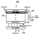
- FIG. 18 is a block diagram showing a configuration of a conventional CAM.
- the conventional CAM 100 includes an input control unit 102, a word block 103 that is a storage area, and an encoder 104.
- the search word is sent to a word block (also referred to as a table) 103 stored from a search line (Search Line, hereinafter abbreviated as SL).
- the number of bits in the CAM 100 is typically 36 to 144 bits.
- the number of word blocks in a typical CAM 100 is on the order of hundreds to 32,000.
- Each input or word circuit contains several dozen CAM cells.
- Each word block 103 has a match line (Match Line, hereinafter abbreviated as ML) indicating whether the search word matches the stored word or not.
- ML Match Line
- the comparison result in each CAM cell according to the input search bit is determined by whether the pass transistor attached to the match line (ML) attached to the CAM cell is off or on.
- ML is connected to the encoder 104.
- the encoder 104 generates a binary matching location (address) in which the ML matches.
- a word block or a word circuit is usually configured by dynamic logic (see Non-Patent Document 12), and is classified into a NOR type (see Non-Patent Document 12) or NAND type (see Non-Patent Documents 13 to 15) structure. ing.
- the pass transistor of the NOR type CAM cell is connected in parallel between the ML and the ground line (also referred to as a ground line), so the word circuit operates at high speed.
- the mismatched word circuit discharges the ML capacity in the NOR type cell with high frequency, and consumes a large amount of power.
- Non-Patent Documents 16 and 17 The NOR type CAM cell is high speed but consumes a lot of power. For this reason, in order to reduce noise and power consumption of ML, a current drive type circuit has been proposed as an attempt to lower the voltage (see Non-Patent Documents 16 and 17).
- the word circuit operates at a medium speed. Since only the matched word circuit discharges the ML capacitor, the power consumption of the NAND type word circuit is lower than that of the NOR type word circuit.
- the NAND-type CAM cell has low power consumption but medium speed. For this reason, a circuit called a PF-CDPD (pseudo-footless clock-and-data precharged dynamic) gate has been proposed in order to increase the throughput of the NAND-type CAM cell (see Non-Patent Documents 14 and 15).
- PF-CDPD pseudo-footless clock-and-data precharged dynamic
- the next searched word is validated after the current search is completed. Since the worst case delay time of the matching operation is usually proportional to the number of bits in a word, the throughput of a conventional synchronous CAM is limited by the number of bits in a CAM word.
- CAM performs parallel search between memory cells storing hundreds of words and input data and outputs matching word addresses.
- the whole is collectively controlled by a clock signal, and the speed is determined by the overall delay due to the bit length of the word circuit.
- IPv6 which is the next generation protocol (communication procedure) of the Internet
- the bit length of the word reaches 144 bits or more, which is a factor for reducing the CAM speed.
- the number of entries to be stored has also increased and the power consumption has increased.
- a word circuit segmentation method for reducing power consumption As a conventional CAM word circuit system, a word circuit segmentation method for reducing power consumption is known. In this method, the first few bits are searched by segmenting the word circuit, matching and mismatching are determined, and the operation of the remaining most of the word circuit is stopped, thereby reducing power consumption. It was. However, in this method, it is necessary to add a sense amplifier or the like between segments, which causes a delay to increase. The delay of the entire word circuit is determined by the sum of the delay of each segment and the delay of each sense amplifier.
- Sheikholeslami “Pipelined Match-Lines and Hierarchical Search-Lines for Low-Power Content-Addressable Memories”, IEEE Custom Integrated Circuits Conference, pp. 383-386, 2003 K. Pagiamtzis and A. Sheikholeslami, “A low-power content-addressable memory (CAM) using pipelined hierarchical search scheme”, IEEE Journal of Solid-State Circuits, vol.39, no.9, pp.1512-1519, pp.1512-1519 . 2004 C. Zukowski and S.-Y. Wang, “Use of selective precharge for low-power on the match lines of content-addressable memories”, Proc.
- the conventional segmentation method in the word circuit for reducing the power of the CAM does not operate at a high speed due to an increase in delay time.
- an object of the present invention is to provide a semiconductor memory device that has a short delay time and operates with low power consumption.
- a semiconductor memory device of the present invention includes an input control unit including a register, a comparator, and a mode control unit, and an associative memory block connected to the input control unit.
- Each word circuit of the memory block includes a k-bit first-stage subword circuit connected to the search line 1 of the input controller and an nk-bit second-stage subword circuit connected to the search line 2 of the input controller.
- the k-bit first-stage subword circuit and the nk-bit second-stage subword circuit are connected via a segmentation circuit.
- the second stage sub-word circuit preferably comprises a further divided sub-sub word circuit, a local match circuit connected to each of the sub-sub word circuits, and a global match circuit of the entire sub-sub word circuit. .
- the sub-subword circuit is preferably k bits.
- the input controller preferably operates in a high speed mode and a low speed mode.
- the input control unit preferably operates in the high-speed mode so as to continue the matching operation continuously with respect to different inputs when it is determined that the k-bit first stage subword does not match the searched word.
- the input control unit preferably operates in a low-speed mode that waits until the search is completed in the associative memory block when it is determined that the k-bit first-stage subword matches the word to be searched.
- each word circuit is charged with a match line before performing the next search, and only the matched match line in the word circuit is a local control signal generated in the word circuit. Is charged.
- each word circuit is charged with the match line before performing the next search, and the match line of the word circuit is charged after the operation of the global match circuit of the word circuit.
- the matching circuit is preferably controlled asynchronously or synchronously for each word.
- the input control unit is preferably driven by a synchronous signal or an asynchronous signal.
- the associative memory block is preferably composed of a binary associative memory cell or a ternary associative memory cell.
- the word circuit is preferably configured to include an autonomous precharge circuit.
- the match circuit is preferably controlled asynchronously for each word, and after a match operation that determines the match between the word to be searched and the stored word, the match line of the matched word is autonomously pre-adjusted by a local control signal. charging, the delay time T PA in autonomous precharged to operate so as not to affect the cycle time T CA of the associative memory block.
- the cycle time of the search operation is determined by the small partial delay in the segmented head partial word circuit, rather than the total delay of the word circuit which should be said to be the worst case. Faster operation than CAM is possible.
- an asynchronous control method is used for independent operation in units of words, so that pipeline registers are not used, power consumption by clock signals is reduced, and at the same time, worst-case delay is not used.
- a circuit can be realized.
- a synchronous circuit can also be realized because of independent operation in units of words.
- It is a block diagram which shows the structure of the semiconductor memory device of this invention. It is a block diagram which shows the structure of an input control part when it is set as m 1. It is a figure which shows the time chart of the input control part which operate
- FIG. 12 is a time chart illustrating the operation of FIG. 11. It is a circuit diagram which shows the word circuit of CAM of this invention.
- FIG. 14 is a time chart showing the operation of the word circuit of FIG. 13. It is a timing chart figure which shows the result of simulation about CAM whose minimum processing size of this invention is 90 nm. It is the figure which compared the cycle time of CAM which carried out the autonomous control of this invention, and CAM of a comparative example. It is a circuit diagram of TCAM. It is a block diagram which shows the structure of the conventional CAM.
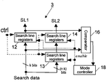
- FIG. 1 is a block diagram showing a configuration of a semiconductor memory device 1 using a word overlapping search (hereinafter abbreviated as a WOS method) of the present invention.
- the semiconductor memory device 1 of the present invention includes a CAM block 2 and an input control unit 3.
- the semiconductor memory device 1 of the present invention is an associative memory and is also called a CAM (abbreviation of content-addressable memory).
- the CAM block 2 includes a word block (a word block is also referred to as a word circuit) 4 that stores an n-bit word, and operates by autonomous control or synchronous control.
- the word block 4 includes a small k-bit subword 4a, a segmentation circuit 5 connected to the k-bit subword 4a, and a (nk) bit subword 4b in the subsequent stage connected to the output side of the segmentation circuit 5. It consists of and. That is, in the word block 4, the small k-bit subword 4 a and the subsequent large (nk) bit subword 4 b are divided via the segmentation circuit 5.
- the k-bit subword 4a is connected to SL1 (search line 1) of the input control unit 3.
- the nk bit subword 4b is connected to SL2 (search line 2) of the input control unit 3.
- Non-Patent Documents 20 and 21 Such a division method is used to reduce the operation rate of the subsequent word block 4 (Non-Patent Documents 20 and 21).
- BCAM binaryCAM
- TCAM tertiaryCAM
- the word to be searched is processed at a speed based on the short delay time (T 1st ) of the first segment than the long delay time (T slow ) of all the word blocks 4. That is, at the same time as the first k-bit search is completed, the k-bit subword 4a is input next. As long as the following k-bit subwords are different, the search word is assigned to a different word block 4 without being used at a rate based on a short delay time (T 1st ). If subsequent subwords are found to be the same, the next search is performed when the current search is completed in both segments.
- the average search time TSA is given by the following equation (2).
- m is the number of subwords in the subsequent stage to be compared.
- the scheduling of input data is controlled by the input control unit 3 that operates synchronously.
- the input control unit 3 includes registers 12 to 14, a k-bit comparator 16, and a mode control unit 18.
- the comparator 16 is also called a comparison circuit or a comparator.
- the mode control unit 18 operates in two modes, high speed and low speed.
- the input control unit 3 is designed by a synchronous circuit method. This method is classified as a prior calculation method because the search word is processed before being searched in the CAM block 2 (Non-Patent Documents 20 and 21).
- the search word is divided into a k-bit subword 4a and an nk bit subword 4b. These subwords are compared in comparator 16 to look for consecutive k-bit subwords that match the same first segment. If these subwords are not the same, the input control unit 3 sends the search word to the CAM block 2 at time T 1st .
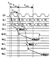
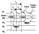
- FIG. 3 is a time chart of the input control unit 3 and the CAM block 2 operating in the high speed mode.
- the input control unit 3 sends a k-bit subword (D1) 4a and an nk bit subword (D2) 4b to the SL1 line and the SL2 line in different cycles.
- D1 1 matches the first segment (ML1 0 ) of k bits, and the matching result is stored (stored) in the segmentation circuit 5.
- subword 4b with D2 1 being n ⁇ k bits matches the segment (ML2 0 ) after k bits.
- D1 2 is processed in another first segment (ML1 0 ).
- the matching operation is an operation for determining a match between a word to be searched and a stored word.
- a circuit that performs this operation is a coincidence circuit. For this reason, it is possible to continue the matching operation continuously for different inputs.
- the input control unit 3 operates in the low speed mode.
- FIG. 4 shows a time chart of the input control unit 3 and the CAM block 2 operating in the low speed mode. Since each word circuit 4 discharges ML once it is determined to match, it is necessary to precharge ML before performing the next search, that is, the matching operation. When consecutive D1s are the same, ML is discharged in the same word circuit 4, and it is necessary to wait until the matching operation in the preceding and succeeding segments is completed and ML pre-charging is completed. As described above, in the low-speed mode, the input control unit 3 stops sending a new search word until the current search is completed in the CAM block 2. The delay time in the low speed mode is given by the following equation (3).
- T reg , T 2nd , and T margin are the delay time from the input control unit 3 to the CAM block 2, the segment delay time after nk bits, and the delay time of mode transition from low speed to high speed, respectively. is there.
- the input control unit 3 After the low speed mode, the input control unit 3 operates in the high speed mode. Actually, when the search word input from the SL of the input control unit 3 matches in the word block 4, the word block 4 cannot be used for Tslow . For this reason, m, which is the number of subwords to be compared in the equation (2), must satisfy the condition given by the following equation (4).
- T 2nd is determined by the delay time of the subsequent segment of nk bits.
- the bit length of the word is 144 bits. That is, when n is 144 and k is 8, as in IPv6, nk is 136.
- the word search is divided into two stages, and the word search of only the first few bits is performed in the first stage search.
- most word circuits 4 can be determined to be inconsistent by word search of the first few bits. Therefore, most of the second long word circuits 4 are not used and the internal state is maintained. Therefore, the next word search can be executed continuously.
- the semiconductor memory device 1 can store the next data after the first-stage search is completed. Word search can be started.
- the speed of the semiconductor memory device 1 does not depend on the bit length of the word as in the conventional CAM, and the high speed operation depending on the partial delay due to the bit length of the small word in the first stage becomes possible.
- phase overlap processing (hereinafter abbreviated as POP) based on autonomous control in the word block 4 of the semiconductor memory device 1 will be described.
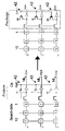
- 5 to 8 show block diagrams of the word circuit 20 of the NAND type cell
- FIG. 5 is a block diagram of precharge
- FIG. 6 is a block diagram in the case of coincidence
- FIG. 7 is a block diagram in the case of mismatch
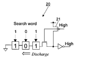
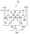
- FIG. FIG. 2 is a circuit diagram of a NAND-type BCAM cell 30 (BCAM cell is also referred to as a word circuit).
- the NAND type word circuit 30 is configured using pass transistors 33 connected in series in a NAND type cell.
- the NAND type word circuit 30 operates in two phases of a precharge phase (precharge) and an evaluation phase (evaluate) by dynamic logic.
- ML also called a match line
- P-type MOS transistor 33e is charged via the P-type MOS transistor 33e.
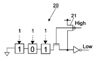
- the search word is the same as the stored word as shown in FIG. 6, all the pass transistors 21 in the CAM cell are on.
- the CAM cell is a memory cell shown in FIG. Therefore, the capacity of the ML line is discharged. This state is called “match”.
- the search word is simplified to “101” and 3 bits.
- the NAND word circuit 20 consumes less power than the NOR word circuit.
- the binary NAND type BCAM cell 30 includes a flip-flop 32 and first to fifth transmission transistors 33 (33a to 33e).
- the transmission transistor is also called a transfer transistor.
- the BCAM cell 30 is provided with ML, SL, and WL (abbreviated as Word Line, also referred to as word line).
- An ML signal is applied to the ML.
- the SL signal is applied to SL.
- a WL signal is applied to WL.
- WL is activated only when a word is written to a cell, and is held at a low level in the search operation.
- all word inputs are stored by BL and BL bar signals, which are complementary signals applied to the bit lines.
- Data “0” and “1” correspond to (0, 1) and (1, 0), respectively.
- search words are assigned to SL, which is a complementary signal applied to SL, and to the SL bar signal.
- the pass transistor 33e connected to the ML is turned on.
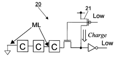
- FIG. 9 is a block diagram of the word circuit 40 by autonomous control based on the phase overlap processing (POP) of the present invention. Only three word circuits 40 are shown. As shown in FIG. 9, each word circuit 40 is controlled by an asynchronous and independent local control signal (lctrl).
- the local control signal (lctrl) is at a high level in the evaluation phase (evaluate) and is at a low level in the precharge phase (precharge).
- the word circuit 40 of the present invention only the ML of the matched word circuit 40 is charged by the local control signal (lctrl) after the previous evaluation phase (evaluate). Since the other local control signals (lctrl) are at the high level, the other word circuits 40 are still in the evaluation phase.
- WOS abbreviation of Word Overlapped Search
- subsequent search words are assigned to other word circuits 40 that are not used. Since the other word circuits 40 that are not used are already charged, the input search word is processed without using the precharge time.
- FIG. 10 is a time chart for explaining the operation of the word circuit 40 by the autonomous control of FIG.
- the ML of the matched word is charged by the local control signal (lctrl).
- the local control signal (lctrl)
- other search words are not used but are assigned to other word circuits 40 in the evaluation phase. Since these phases are carried out in duplicate, delay time of the pre-charging phase T PA does not affect the cycle time T CA.
- the autonomous control based on the POP operation serves to hide the delay time T PA of the pre-charging phase.
- delay time T SA of the evaluation phase longer than the delay time of the pre-charging phase T PA. Therefore, the cycle time T CA is given by the following equation (6).
- phase overlap processing (POP) based on autonomous control in the word block 4 of the CAM block 2 may be a conventional synchronous type.
- FIG. 11 is a block diagram of the synchronous word circuit 42
- FIG. 12 is a time chart for explaining the operation of FIG.
- a clock signal that is a global control signal is applied to the gate of each charging transistor 21.
- a high level clock signal is applied in the evaluation phase
- a low level clock signal is applied in the precharge phase. Therefore, the CAM cycle time (T CS ) in which the word circuit 42 is a synchronous type is given by the following equation (7).
- T SS is the search time given by equation (5), that is, the delay time of the evaluation phase
- T PS is the delay time of the precharge phase.
- T SS is longer than T PS , and these delay times are the same in the synchronous CAM. Therefore, the equation (7) is expressed by the following equation (8).
- the duty ratio of the clock signal in the synchronous circuit is 50%.
- the clock cycle is in the evaluation phase period as shown in equation (8). Twice as much.
- the throughput ratio of the semiconductor memory device 1 of the present invention to the conventional synchronous CAM is given by the following equation (9).
- the delay time T SA of the evaluation phase is approximately equal to T 1st .
- FIG. 13 is a circuit diagram showing a word circuit 50 including WOS and POP.
- the word circuit 50 of the present invention includes an 8-bit first stage subword circuit 54a, a segmentation circuit 55, an autonomous precharge circuit 56, and a 136 bit second stage subword circuit 54b. It is configured to include.
- an 8-bit first stage subword circuit 54a includes eight NAND cells 58, a P-type MOS transistor 60 for autonomous precharging, a weak feedback P-type MOS transistor 62, It is composed of
- ML is charged by a P-type MOS transistor 60 for autonomous precharging controlled by the autonomous precharging circuit 56.
- the weak feedback P-type MOS transistor 62 is used to solve the problem of ML charge distribution by the NAND cell 58 (see Non-Patent Documents 14, 15, and 24).
- ML1 0 is connected to the autonomous precharge circuit 56 is connected to the second-stage sub-word circuit 54b of 136 bits.
- the 136-bit second-stage subword circuit 54 b includes 17 local match circuits 70 and a global match circuit 72.
- a match circuit is a circuit that determines a match between a word to be searched and a stored word.
- a circuit that performs this operation is a coincidence circuit.
- Such a hierarchical design divides the word circuit 50 into a local match circuit 70 and a global match circuit 72 (see Non-Patent Document 25).
- each local match circuit 70 includes an inverter 71, a P-type MOS transistor 60 for autonomous precharging, a weak feedback P-type MOS transistor 62, and eight NAND cells (sub-cells). - a subword circuit) 58, an output ML1 0 segmentation circuit 55 is composed of N-type MOS transistor 74. issued enter the gate. Once ML1 0 is asserted, that is effective, with 17 local matching circuit 70 operates. In other cases, since the 8-bit first stage subword circuit 54a does not match, the 17 local match circuits 70 do not operate.
- the remaining 136-bit subword 54b is sent in parallel from the input control unit 3, and is divided into 17 sub-subwords by 8 bits. Each sub-subword is processed by the local match circuit 70.
- the output (LMLi 0 (0 ⁇ i ⁇ 17)) of the local match circuit 70 is at a high level when the input sub-subwords match, and is at the low level when the input sub-subwords do not match. .
- the delay time from ML1 0 to LMLi 0 is defined by T 2ndL .
- the global match circuit 72 includes 17 N-type MOS transistors 74 connected in series, a P-type MOS transistor 60 for autonomous precharging, and a weak feedback P-type MOS transistor 62. And an inverter 71.
- the outputs of LMLi 0 are input to the gates of 17 series-connected N-type MOS transistors 74 of the global match circuit 72.
- the output ML2 0 global matching circuit 72 is enabled, i.e. high level is outputted. This state means that the search word matches the stored word. In other states, ML2 0 is at a low level.
- T 2ndG Delay time until a transition from LMLi 0 to ML2 0 is defined by T 2ndG. From this, the delay time T 2nd in the second-stage segment 54b is given by the following equation (11).
- the autonomous precharge circuit 56 shown in FIG. 13C is also operating. As shown in FIG. 13C, the autonomous precharge circuit 56 is a circuit in which AND gates 78 are connected in series. When ML1 0 is asserted, ie, enabled, a delay time T delay is defined.
- the output of the autonomous precharge circuit 56 becomes invalid after the delay time T delay . Then, the autonomous precharge circuit 56 charges all MLs of the word circuit 50.
- FIG. 14 is a time chart showing the operation of the word circuit 50 of FIG.
- the search word is divided into 8-bit sub-word and 136-bit sub-word, it is sent from the input control unit 3 at a rate based on the period of T CA.
- the 8-bit subword 54a matches in the first segment, the remaining 136-bit subword 54b is processed later.
- Search word since changes based on the period of T CA, is the 136-bit word is required to be assigned, that is effective in the local matching circuit 70 within the T CA. For this reason, the delay time of the local matching circuit 70 needs to satisfy the condition of the following equation (12).
- the global match circuit 72 determines whether or not the search words match. At the same time, the autonomous precharge circuit 56 operates.
- the delay time T delay needs to satisfy the condition of the following equation (13).
- T slow needs to satisfy the condition of the following formula (14).
- T prec is a delay time of precharging of all MLs.
- the cycle time T CA shown in FIGS. 10 and 14 is approximately T 1st .
- the 256 ⁇ 144-bit semiconductor memory device 1, 1A of the present invention will be described.
- the 256 ⁇ 144-bit semiconductor memory device 1 or 1A of the present invention is compared with a conventional synchronous CAM using the segment method.
- the bit number (nk) of the second-stage subword is 136 bits.
- the semiconductor memory devices 1 and 1A of the present invention have the same word configuration.
- the configuration of the second-stage subword in the semiconductor memory devices 1 and 1A of the present invention is hierarchical (see Non-Patent Document 25 for hierarchical subwords).
- the semiconductor memory devices 1 and 1A of the present invention and the comparative example have been evaluated based on 90 nm CMOS technology.
- the words to be stored have a uniform random number distribution.
- 90 nm is the minimum processing dimension of the CMOS manufacturing process used.
- Table 1 is a table showing the delay time of each circuit of the semiconductor memory device 1 of the present invention.
- the semiconductor memory device 1 of the present invention was evaluated using HSPICE (SPICE (Simulation Program with Integrated Circuit Emphasis) manufactured by Synopsys) as software.
- the autonomous precharge circuit 56 was designed to satisfy the expression (13).
- m was set to 3.
- T reg is 51ps
- T 1st is 259ps
- T 2ndL is 225ps
- T 2ndG is 243ps
- T delay is 500 ps
- T prec is 81 ps.
- FIG. 15 is a timing chart showing simulation results for the semiconductor memory devices 1 and 1A in the 90 nm CMOS process of the present invention. As shown in FIG. 15, search word followed by a so allocated to different word circuit without using the semiconductor memory device 1,1A of the present invention operates at T CA based on short cycle delay.
- FIG. 16 is a diagram comparing the cycle times of the CAMs of the semiconductor memory devices 1 and 1A that are autonomously controlled according to the present invention and the comparative example.
- the CAM cycle time of the comparative example is determined by equation (7) and is 1454 ps.
- the cycle time of the semiconductor memory device 1 using the WOS of the present invention operates with the delay time of the first-stage subword circuit. Therefore, the cycle time of the semiconductor memory device 1 using the WOS of the present invention is 555 ps, which is 64.1% lower than that of the conventional CAM.
- the cycle time of the semiconductor memory device 1A using the WOS and POP of the present invention is reduced by 82% as compared with the conventional CAM because the influence of the precharge delay time is eliminated, and the cycle time is about 261 ps. To do.
- the power consumption of the semiconductor memory devices 1 and 1A is given by the following (16).
- E match , E search , and E ctrl are the power consumption of the ML, SL, and control signals, respectively.
- the local match circuit 70 does not operate. Furthermore, the global match circuit 72 operates only when each sub-subword matches the local match circuit 70. Therefore, the power consumption of ML is given by the following equation (17).
- E 1st, E 2ndL, E 2ndG each first-stage sub-word circuit 54a, the local matching circuit 70, a power consumption of global matching circuit 72.
- ML switching probability is very low and SL changes when a new search word is assigned.
- Ectrl which is the power consumption of the control signal, is related to the clock signal, which is a global control signal, in the conventional synchronous CAM.
- the clock signal turns on all P-type MOS transistors 60 for autonomous precharging (see FIG. 10). For this reason, Ectrl (sync) , which is the power consumption of the conventional synchronous CAM control signal, is given by the following equation (18).
- E clk_ buffer
- E prec the power consumption of all the P-type MOS transistors 60 for autonomous precharging.
- the power consumption Ectrl (self) of the input signal of the semiconductor memory device 1A of the present invention is related to the local control signal (lctrl) of the semiconductor memory device 1A by autonomous control. Since only the precharge transistor in the matched word circuit is turned on by the prec signal (precharge signal), the power consumption for charging the precharge P-type MOSFET 60 is reduced. Further, the precharge circuit 56 operates only when the first-stage segments match. For this reason, Ectrl (self) which is the power consumption of the control signal of the semiconductor memory device 1A of the present invention is given by the following equation (19).
- E self_precharge is the power consumption of the precharge circuit.
- Table 2 is a table comparing the power consumption of the semiconductor memory device 1A of the present invention and the CAM of the comparative example. The average cycle time and the number of transistors used are also shown. The average cycle time of the semiconductor memory device 1A of the present invention is 261 ps, and the average cycle time of the synchronous CAM of the comparative example is 1454 ps. From this, it can be seen that the throughput of the semiconductor memory device 1A of the present invention is 5.57 times the CAM of the comparative example.
- the semiconductor memory device 1A of the present invention uses the local control signal (lctrl) and the power consumption of the control signal is reduced, the total power consumption is reduced to 61.6% of the synchronous CAM of the comparative example. .
- the word circuit is locally controlled, an autonomous precharge control circuit is required. For this reason, the area of the CAM of the present invention is very small but increases by 8%.
- the number of transistors of the semiconductor memory device 1A of the present invention is 408k (408,000), and the number of transistors of the synchronous CAM of the comparative example is 372k (372,000).
- Table 3 is a table comparing the semiconductor memory device 1A of the present invention with a conventional example.
- the advantages of the hybrid type are low power consumption and high-speed operation, which depend on the NAND type cell and the NOR type cell, respectively.
- the cycle time was shortened to 8% and the energy consumption / bit per search was reduced to 23% as compared with the hybrid type CAM having a minimum processing dimension of 0.1 ⁇ m.
- the semiconductor memory device 1A according to the present invention operates at a speed about three times that of a NAND CAM having a minimum processing dimension of 65 nm.
- FIG. 17 is a circuit diagram of the TCAM 80.
- the TCAM 80 has a configuration in which two BCAM memory cells 30 shown in FIG. 8 are arranged in parallel to the match line (ML).
- the TCAM 80 includes a NAND first memory cell 81 that stores upper “0” and “1”, a NAND second memory cell 82 that stores lower “X”, and a plurality of transmissions. For example, and an ML transmission transistor 85.
- WL, BL / SL, and BL bar / SL bar are connected to the NAND-type first memory cell 81.
- WL, DCL (don't care line), and DCL bar are connected to the NAND type second memory cell 82.
- the ML is connected to the NAND-type first memory cell 81 and the NAND-type second memory cell 82 through the ML transmission transistor 85.
- the CAM block 2 of the semiconductor memory device 1 and 1A shown in FIG. 1 is the TCAM 80 shown as an example in FIG. 17, and the input control unit 3 and the like are changed from binary to ternary data.
- 1A operates as an associative memory of ternary data.
Landscapes
- Engineering & Computer Science (AREA)
- Databases & Information Systems (AREA)
- Theoretical Computer Science (AREA)
- Static Random-Access Memory (AREA)
- Microelectronics & Electronic Packaging (AREA)
- Computational Linguistics (AREA)
- Data Mining & Analysis (AREA)
- Physics & Mathematics (AREA)
- General Engineering & Computer Science (AREA)
- General Physics & Mathematics (AREA)
- Compression, Expansion, Code Conversion, And Decoders (AREA)
Priority Applications (2)
| Application Number | Priority Date | Filing Date | Title |
|---|---|---|---|
| KR1020147034459A KR101948126B1 (ko) | 2012-05-06 | 2013-05-03 | 반도체 기억 장치 |
| US14/399,041 US9324429B2 (en) | 2012-05-06 | 2013-05-03 | Semiconductor storage device |
Applications Claiming Priority (2)
| Application Number | Priority Date | Filing Date | Title |
|---|---|---|---|
| JP2012105558A JP5998381B2 (ja) | 2012-05-06 | 2012-05-06 | 半導体記憶装置 |
| JP2012-105558 | 2012-05-06 |
Publications (1)
| Publication Number | Publication Date |
|---|---|
| WO2013168685A1 true WO2013168685A1 (ja) | 2013-11-14 |
Family
ID=49550722
Family Applications (1)
| Application Number | Title | Priority Date | Filing Date |
|---|---|---|---|
| PCT/JP2013/062791 Ceased WO2013168685A1 (ja) | 2012-05-06 | 2013-05-03 | 半導体記憶装置 |
Country Status (4)
| Country | Link |
|---|---|
| US (1) | US9324429B2 (enExample) |
| JP (1) | JP5998381B2 (enExample) |
| KR (1) | KR101948126B1 (enExample) |
| WO (1) | WO2013168685A1 (enExample) |
Cited By (1)
| Publication number | Priority date | Publication date | Assignee | Title |
|---|---|---|---|---|
| JP2015523670A (ja) * | 2012-05-29 | 2015-08-13 | インターナショナル・ビジネス・マシーンズ・コーポレーションInternational Business Machines Corporation | 連想メモリ(cam)を検索するためのシステム及び方法 |
Families Citing this family (3)
| Publication number | Priority date | Publication date | Assignee | Title |
|---|---|---|---|---|
| KR101714984B1 (ko) * | 2016-08-29 | 2017-03-09 | 인하대학교 산학협력단 | 지역적 셀프 리셋팅 동작을 하는 회로의 방법 및 장치 |
| TWI713051B (zh) * | 2019-10-21 | 2020-12-11 | 瑞昱半導體股份有限公司 | 內容可定址記憶體裝置 |
| CN112735495B (zh) * | 2019-10-28 | 2024-11-22 | 瑞昱半导体股份有限公司 | 内容可定址存储器装置 |
Citations (5)
| Publication number | Priority date | Publication date | Assignee | Title |
|---|---|---|---|---|
| JPH02308499A (ja) * | 1989-05-23 | 1990-12-21 | Toshiba Corp | 連想メモリ |
| JPH03212896A (ja) * | 1990-01-16 | 1991-09-18 | Mitsubishi Electric Corp | 連想記憶装置 |
| JPH06333395A (ja) * | 1993-05-19 | 1994-12-02 | Kawasaki Steel Corp | 連想メモリ |
| JPH0714391A (ja) * | 1993-06-22 | 1995-01-17 | Kawasaki Steel Corp | 半導体記憶装置 |
| JP2013037750A (ja) * | 2011-08-10 | 2013-02-21 | Renesas Electronics Corp | 内容参照メモリ |
Family Cites Families (7)
| Publication number | Priority date | Publication date | Assignee | Title |
|---|---|---|---|---|
| US3997882A (en) * | 1975-04-01 | 1976-12-14 | Burroughs Corporation | Content addressable memory system employing charge coupled device storage and directory registers and N/(1-H) counter refresh synchronization |
| US5485418A (en) | 1990-01-16 | 1996-01-16 | Mitsubishi Denki Kabushiki Kaisha | Associative memory |
| JP2002197873A (ja) * | 2000-12-27 | 2002-07-12 | Kawasaki Microelectronics Kk | 連想メモリ |
| JP2002237190A (ja) | 2001-02-07 | 2002-08-23 | Kawasaki Microelectronics Kk | 連想メモリ装置およびその構成方法 |
| JP4552689B2 (ja) | 2005-02-28 | 2010-09-29 | 株式会社日立製作所 | 半導体記憶装置 |
| JP4861012B2 (ja) * | 2005-03-31 | 2012-01-25 | ルネサスエレクトロニクス株式会社 | Cam装置 |
| US7426127B2 (en) | 2006-12-21 | 2008-09-16 | Intel Corporation | Full-rail, dual-supply global bitline accelerator CAM circuit |
-
2012
- 2012-05-06 JP JP2012105558A patent/JP5998381B2/ja active Active
-
2013
- 2013-05-03 KR KR1020147034459A patent/KR101948126B1/ko active Active
- 2013-05-03 US US14/399,041 patent/US9324429B2/en active Active
- 2013-05-03 WO PCT/JP2013/062791 patent/WO2013168685A1/ja not_active Ceased
Patent Citations (5)
| Publication number | Priority date | Publication date | Assignee | Title |
|---|---|---|---|---|
| JPH02308499A (ja) * | 1989-05-23 | 1990-12-21 | Toshiba Corp | 連想メモリ |
| JPH03212896A (ja) * | 1990-01-16 | 1991-09-18 | Mitsubishi Electric Corp | 連想記憶装置 |
| JPH06333395A (ja) * | 1993-05-19 | 1994-12-02 | Kawasaki Steel Corp | 連想メモリ |
| JPH0714391A (ja) * | 1993-06-22 | 1995-01-17 | Kawasaki Steel Corp | 半導体記憶装置 |
| JP2013037750A (ja) * | 2011-08-10 | 2013-02-21 | Renesas Electronics Corp | 内容参照メモリ |
Cited By (1)
| Publication number | Priority date | Publication date | Assignee | Title |
|---|---|---|---|---|
| JP2015523670A (ja) * | 2012-05-29 | 2015-08-13 | インターナショナル・ビジネス・マシーンズ・コーポレーションInternational Business Machines Corporation | 連想メモリ(cam)を検索するためのシステム及び方法 |
Also Published As
| Publication number | Publication date |
|---|---|
| US9324429B2 (en) | 2016-04-26 |
| JP2013235620A (ja) | 2013-11-21 |
| KR101948126B1 (ko) | 2019-02-14 |
| KR20150014487A (ko) | 2015-02-06 |
| US20150109842A1 (en) | 2015-04-23 |
| JP5998381B2 (ja) | 2016-09-28 |
Similar Documents
| Publication | Publication Date | Title |
|---|---|---|
| Onizawa et al. | High-throughput low-energy content-addressable memory based on self-timed overlapped search mechanism | |
| US6392910B1 (en) | Priority encoder with multiple match function for content addressable memories and methods for implementing the same | |
| Imani et al. | MASC: Ultra-low energy multiple-access single-charge TCAM for approximate computing | |
| Huan et al. | A low-power accelerator for deep neural networks with enlarged near-zero sparsity | |
| Mahendra et al. | Energy-efficient precharge-free ternary content addressable memory (TCAM) for high search rate applications | |
| Imani et al. | ReMAM: Low energy resistive multi-stage associative memory for energy efficient computing | |
| Jarollahi et al. | Algorithm and architecture for a low-power content-addressable memory based on sparse clustered networks | |
| Onizawa et al. | High-throughput low-energy self-timed CAM based on reordered overlapped search mechanism | |
| Hussain et al. | Match-line division and control to reduce power dissipation in content addressable memory | |
| CN103069497B (zh) | 减少内容可寻址存储器的电力使用的系统和方法 | |
| JP5998381B2 (ja) | 半導体記憶装置 | |
| Imani et al. | CAP: Configurable resistive associative processor for near-data computing | |
| CN110324204A (zh) | 一种在fpga中实现的高速正则表达式匹配引擎及方法 | |
| Karthik et al. | Design and Implementation of a Low Power Ternary Content Addressable Memory (TCAM) | |
| CN101859596A (zh) | 一种内容可寻址存储器 | |
| Onizawa et al. | High-throughput CAM based on a synchronous overlapped search scheme | |
| US20160358654A1 (en) | Low-power ternary content addressable memory | |
| Jiang et al. | A fully parallel content addressable memory design using multi-bank structure | |
| Devi et al. | Low Energy Asynchronous CAM Based On Reordered Overlapped Search Mechanism | |
| Alrushood et al. | Improving energy consumption in content-addressable memory through precomputation | |
| CN114758704A (zh) | 内容可寻址存储器及其操作方法 | |
| Chen et al. | Filter-based dual-voltage architecture for low-power long-word TCAM design | |
| Mahendra et al. | Design and implementation of drivers and selectors for content addressable memory (CAM) | |
| Muralidharan et al. | Low power content addressable memory using common match line scheme for high performance processors | |
| Hussain et al. | Pseudo-static master-slave match-line scheme for sustainable-performance and energy-efficient content addressable memory |
Legal Events
| Date | Code | Title | Description |
|---|---|---|---|
| 121 | Ep: the epo has been informed by wipo that ep was designated in this application |
Ref document number: 13787419 Country of ref document: EP Kind code of ref document: A1 |
|
| WWE | Wipo information: entry into national phase |
Ref document number: 14399041 Country of ref document: US |
|
| NENP | Non-entry into the national phase |
Ref country code: DE |
|
| ENP | Entry into the national phase |
Ref document number: 20147034459 Country of ref document: KR Kind code of ref document: A |
|
| 122 | Ep: pct application non-entry in european phase |
Ref document number: 13787419 Country of ref document: EP Kind code of ref document: A1 |