WO2013168685A1 - Semiconductor storage device - Google Patents
Semiconductor storage device Download PDFInfo
- Publication number
- WO2013168685A1 WO2013168685A1 PCT/JP2013/062791 JP2013062791W WO2013168685A1 WO 2013168685 A1 WO2013168685 A1 WO 2013168685A1 JP 2013062791 W JP2013062791 W JP 2013062791W WO 2013168685 A1 WO2013168685 A1 WO 2013168685A1
- Authority
- WO
- WIPO (PCT)
- Prior art keywords
- word
- circuit
- semiconductor memory
- memory device
- search
- Prior art date
Links
Images


Classifications
-
- G—PHYSICS
- G11—INFORMATION STORAGE
- G11C—STATIC STORES
- G11C15/00—Digital stores in which information comprising one or more characteristic parts is written into the store and in which information is read-out by searching for one or more of these characteristic parts, i.e. associative or content-addressed stores
- G11C15/04—Digital stores in which information comprising one or more characteristic parts is written into the store and in which information is read-out by searching for one or more of these characteristic parts, i.e. associative or content-addressed stores using semiconductor elements
-
- G—PHYSICS
- G06—COMPUTING; CALCULATING OR COUNTING
- G06F—ELECTRIC DIGITAL DATA PROCESSING
- G06F16/00—Information retrieval; Database structures therefor; File system structures therefor
- G06F16/90—Details of database functions independent of the retrieved data types
- G06F16/903—Querying
- G06F16/90335—Query processing
- G06F16/90339—Query processing by using parallel associative memories or content-addressable memories
-
- G—PHYSICS
- G11—INFORMATION STORAGE
- G11C—STATIC STORES
- G11C15/00—Digital stores in which information comprising one or more characteristic parts is written into the store and in which information is read-out by searching for one or more of these characteristic parts, i.e. associative or content-addressed stores
-
- G—PHYSICS
- G11—INFORMATION STORAGE
- G11C—STATIC STORES
- G11C7/00—Arrangements for writing information into, or reading information out from, a digital store
- G11C7/12—Bit line control circuits, e.g. drivers, boosters, pull-up circuits, pull-down circuits, precharging circuits, equalising circuits, for bit lines
-
- G—PHYSICS
- G11—INFORMATION STORAGE
- G11C—STATIC STORES
- G11C8/00—Arrangements for selecting an address in a digital store
- G11C8/08—Word line control circuits, e.g. drivers, boosters, pull-up circuits, pull-down circuits, precharging circuits, for word lines
Definitions
- the present invention relates to a semiconductor memory device. More specifically, the present invention relates to a semiconductor memory device that operates at high speed and with low power consumption.
- CAM Content-addressable memory
- the CAM has a look-up table function that compares an input search word with a stored word, and the CAM outputs words that are matched in a completely parallel and equal search method at a high speed.
- Non-Patent Document 1 is a parametric curve extraction (see Non-Patent Document 1), a Hough transform (see Non-Patent Document 2) used in a feature extraction method of digital image processing conversion, and Lempel-Ziv, which is a kind of data compression algorithm.
- Conversion see non-patent document 3
- human body communication control device see non-patent document 4
- cyclic event generator see non-patent document 5
- cache memory see non-patent document 6
- virus detection processor is a kind of data compression algorithm.
- CAM is mainly used for packet control of network routers and network switches (see Non-Patent Documents 8 to 11).
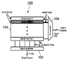
- FIG. 18 is a block diagram showing a configuration of a conventional CAM.
- the conventional CAM 100 includes an input control unit 102, a word block 103 that is a storage area, and an encoder 104.
- the search word is sent to a word block (also referred to as a table) 103 stored from a search line (Search Line, hereinafter abbreviated as SL).
- the number of bits in the CAM 100 is typically 36 to 144 bits.
- the number of word blocks in a typical CAM 100 is on the order of hundreds to 32,000.
- Each input or word circuit contains several dozen CAM cells.
- Each word block 103 has a match line (Match Line, hereinafter abbreviated as ML) indicating whether the search word matches the stored word or not.
- ML Match Line
- the comparison result in each CAM cell according to the input search bit is determined by whether the pass transistor attached to the match line (ML) attached to the CAM cell is off or on.
- ML is connected to the encoder 104.
- the encoder 104 generates a binary matching location (address) in which the ML matches.
- a word block or a word circuit is usually configured by dynamic logic (see Non-Patent Document 12), and is classified into a NOR type (see Non-Patent Document 12) or NAND type (see Non-Patent Documents 13 to 15) structure. ing.
- the pass transistor of the NOR type CAM cell is connected in parallel between the ML and the ground line (also referred to as a ground line), so the word circuit operates at high speed.
- the mismatched word circuit discharges the ML capacity in the NOR type cell with high frequency, and consumes a large amount of power.
- Non-Patent Documents 16 and 17 The NOR type CAM cell is high speed but consumes a lot of power. For this reason, in order to reduce noise and power consumption of ML, a current drive type circuit has been proposed as an attempt to lower the voltage (see Non-Patent Documents 16 and 17).
- the word circuit operates at a medium speed. Since only the matched word circuit discharges the ML capacitor, the power consumption of the NAND type word circuit is lower than that of the NOR type word circuit.
- the NAND-type CAM cell has low power consumption but medium speed. For this reason, a circuit called a PF-CDPD (pseudo-footless clock-and-data precharged dynamic) gate has been proposed in order to increase the throughput of the NAND-type CAM cell (see Non-Patent Documents 14 and 15).
- PF-CDPD pseudo-footless clock-and-data precharged dynamic
- the next searched word is validated after the current search is completed. Since the worst case delay time of the matching operation is usually proportional to the number of bits in a word, the throughput of a conventional synchronous CAM is limited by the number of bits in a CAM word.
- CAM performs parallel search between memory cells storing hundreds of words and input data and outputs matching word addresses.
- the whole is collectively controlled by a clock signal, and the speed is determined by the overall delay due to the bit length of the word circuit.
- IPv6 which is the next generation protocol (communication procedure) of the Internet
- the bit length of the word reaches 144 bits or more, which is a factor for reducing the CAM speed.
- the number of entries to be stored has also increased and the power consumption has increased.
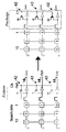
- a word circuit segmentation method for reducing power consumption As a conventional CAM word circuit system, a word circuit segmentation method for reducing power consumption is known. In this method, the first few bits are searched by segmenting the word circuit, matching and mismatching are determined, and the operation of the remaining most of the word circuit is stopped, thereby reducing power consumption. It was. However, in this method, it is necessary to add a sense amplifier or the like between segments, which causes a delay to increase. The delay of the entire word circuit is determined by the sum of the delay of each segment and the delay of each sense amplifier.
- Sheikholeslami “Pipelined Match-Lines and Hierarchical Search-Lines for Low-Power Content-Addressable Memories”, IEEE Custom Integrated Circuits Conference, pp. 383-386, 2003 K. Pagiamtzis and A. Sheikholeslami, “A low-power content-addressable memory (CAM) using pipelined hierarchical search scheme”, IEEE Journal of Solid-State Circuits, vol.39, no.9, pp.1512-1519, pp.1512-1519 . 2004 C. Zukowski and S.-Y. Wang, “Use of selective precharge for low-power on the match lines of content-addressable memories”, Proc.
- the conventional segmentation method in the word circuit for reducing the power of the CAM does not operate at a high speed due to an increase in delay time.
- an object of the present invention is to provide a semiconductor memory device that has a short delay time and operates with low power consumption.
- a semiconductor memory device of the present invention includes an input control unit including a register, a comparator, and a mode control unit, and an associative memory block connected to the input control unit.
- Each word circuit of the memory block includes a k-bit first-stage subword circuit connected to the search line 1 of the input controller and an nk-bit second-stage subword circuit connected to the search line 2 of the input controller.
- the k-bit first-stage subword circuit and the nk-bit second-stage subword circuit are connected via a segmentation circuit.
- the second stage sub-word circuit preferably comprises a further divided sub-sub word circuit, a local match circuit connected to each of the sub-sub word circuits, and a global match circuit of the entire sub-sub word circuit. .
- the sub-subword circuit is preferably k bits.
- the input controller preferably operates in a high speed mode and a low speed mode.
- the input control unit preferably operates in the high-speed mode so as to continue the matching operation continuously with respect to different inputs when it is determined that the k-bit first stage subword does not match the searched word.
- the input control unit preferably operates in a low-speed mode that waits until the search is completed in the associative memory block when it is determined that the k-bit first-stage subword matches the word to be searched.
- each word circuit is charged with a match line before performing the next search, and only the matched match line in the word circuit is a local control signal generated in the word circuit. Is charged.
- each word circuit is charged with the match line before performing the next search, and the match line of the word circuit is charged after the operation of the global match circuit of the word circuit.
- the matching circuit is preferably controlled asynchronously or synchronously for each word.
- the input control unit is preferably driven by a synchronous signal or an asynchronous signal.
- the associative memory block is preferably composed of a binary associative memory cell or a ternary associative memory cell.
- the word circuit is preferably configured to include an autonomous precharge circuit.
- the match circuit is preferably controlled asynchronously for each word, and after a match operation that determines the match between the word to be searched and the stored word, the match line of the matched word is autonomously pre-adjusted by a local control signal. charging, the delay time T PA in autonomous precharged to operate so as not to affect the cycle time T CA of the associative memory block.
- the cycle time of the search operation is determined by the small partial delay in the segmented head partial word circuit, rather than the total delay of the word circuit which should be said to be the worst case. Faster operation than CAM is possible.
- an asynchronous control method is used for independent operation in units of words, so that pipeline registers are not used, power consumption by clock signals is reduced, and at the same time, worst-case delay is not used.
- a circuit can be realized.
- a synchronous circuit can also be realized because of independent operation in units of words.
- It is a block diagram which shows the structure of the semiconductor memory device of this invention. It is a block diagram which shows the structure of an input control part when it is set as m 1. It is a figure which shows the time chart of the input control part which operate
- FIG. 12 is a time chart illustrating the operation of FIG. 11. It is a circuit diagram which shows the word circuit of CAM of this invention.
- FIG. 14 is a time chart showing the operation of the word circuit of FIG. 13. It is a timing chart figure which shows the result of simulation about CAM whose minimum processing size of this invention is 90 nm. It is the figure which compared the cycle time of CAM which carried out the autonomous control of this invention, and CAM of a comparative example. It is a circuit diagram of TCAM. It is a block diagram which shows the structure of the conventional CAM.
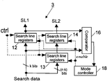
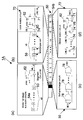
- FIG. 1 is a block diagram showing a configuration of a semiconductor memory device 1 using a word overlapping search (hereinafter abbreviated as a WOS method) of the present invention.
- the semiconductor memory device 1 of the present invention includes a CAM block 2 and an input control unit 3.
- the semiconductor memory device 1 of the present invention is an associative memory and is also called a CAM (abbreviation of content-addressable memory).
- the CAM block 2 includes a word block (a word block is also referred to as a word circuit) 4 that stores an n-bit word, and operates by autonomous control or synchronous control.
- the word block 4 includes a small k-bit subword 4a, a segmentation circuit 5 connected to the k-bit subword 4a, and a (nk) bit subword 4b in the subsequent stage connected to the output side of the segmentation circuit 5. It consists of and. That is, in the word block 4, the small k-bit subword 4 a and the subsequent large (nk) bit subword 4 b are divided via the segmentation circuit 5.
- the k-bit subword 4a is connected to SL1 (search line 1) of the input control unit 3.
- the nk bit subword 4b is connected to SL2 (search line 2) of the input control unit 3.
- Non-Patent Documents 20 and 21 Such a division method is used to reduce the operation rate of the subsequent word block 4 (Non-Patent Documents 20 and 21).
- BCAM binaryCAM
- TCAM tertiaryCAM
- the word to be searched is processed at a speed based on the short delay time (T 1st ) of the first segment than the long delay time (T slow ) of all the word blocks 4. That is, at the same time as the first k-bit search is completed, the k-bit subword 4a is input next. As long as the following k-bit subwords are different, the search word is assigned to a different word block 4 without being used at a rate based on a short delay time (T 1st ). If subsequent subwords are found to be the same, the next search is performed when the current search is completed in both segments.
- the average search time TSA is given by the following equation (2).
- m is the number of subwords in the subsequent stage to be compared.
- the scheduling of input data is controlled by the input control unit 3 that operates synchronously.
- the input control unit 3 includes registers 12 to 14, a k-bit comparator 16, and a mode control unit 18.
- the comparator 16 is also called a comparison circuit or a comparator.
- the mode control unit 18 operates in two modes, high speed and low speed.
- the input control unit 3 is designed by a synchronous circuit method. This method is classified as a prior calculation method because the search word is processed before being searched in the CAM block 2 (Non-Patent Documents 20 and 21).
- the search word is divided into a k-bit subword 4a and an nk bit subword 4b. These subwords are compared in comparator 16 to look for consecutive k-bit subwords that match the same first segment. If these subwords are not the same, the input control unit 3 sends the search word to the CAM block 2 at time T 1st .
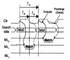
- FIG. 3 is a time chart of the input control unit 3 and the CAM block 2 operating in the high speed mode.
- the input control unit 3 sends a k-bit subword (D1) 4a and an nk bit subword (D2) 4b to the SL1 line and the SL2 line in different cycles.
- D1 1 matches the first segment (ML1 0 ) of k bits, and the matching result is stored (stored) in the segmentation circuit 5.
- subword 4b with D2 1 being n ⁇ k bits matches the segment (ML2 0 ) after k bits.
- D1 2 is processed in another first segment (ML1 0 ).
- the matching operation is an operation for determining a match between a word to be searched and a stored word.
- a circuit that performs this operation is a coincidence circuit. For this reason, it is possible to continue the matching operation continuously for different inputs.
- the input control unit 3 operates in the low speed mode.
- FIG. 4 shows a time chart of the input control unit 3 and the CAM block 2 operating in the low speed mode. Since each word circuit 4 discharges ML once it is determined to match, it is necessary to precharge ML before performing the next search, that is, the matching operation. When consecutive D1s are the same, ML is discharged in the same word circuit 4, and it is necessary to wait until the matching operation in the preceding and succeeding segments is completed and ML pre-charging is completed. As described above, in the low-speed mode, the input control unit 3 stops sending a new search word until the current search is completed in the CAM block 2. The delay time in the low speed mode is given by the following equation (3).
- T reg , T 2nd , and T margin are the delay time from the input control unit 3 to the CAM block 2, the segment delay time after nk bits, and the delay time of mode transition from low speed to high speed, respectively. is there.
- the input control unit 3 After the low speed mode, the input control unit 3 operates in the high speed mode. Actually, when the search word input from the SL of the input control unit 3 matches in the word block 4, the word block 4 cannot be used for Tslow . For this reason, m, which is the number of subwords to be compared in the equation (2), must satisfy the condition given by the following equation (4).
- T 2nd is determined by the delay time of the subsequent segment of nk bits.
- the bit length of the word is 144 bits. That is, when n is 144 and k is 8, as in IPv6, nk is 136.
- the word search is divided into two stages, and the word search of only the first few bits is performed in the first stage search.
- most word circuits 4 can be determined to be inconsistent by word search of the first few bits. Therefore, most of the second long word circuits 4 are not used and the internal state is maintained. Therefore, the next word search can be executed continuously.
- the semiconductor memory device 1 can store the next data after the first-stage search is completed. Word search can be started.
- the speed of the semiconductor memory device 1 does not depend on the bit length of the word as in the conventional CAM, and the high speed operation depending on the partial delay due to the bit length of the small word in the first stage becomes possible.
- phase overlap processing (hereinafter abbreviated as POP) based on autonomous control in the word block 4 of the semiconductor memory device 1 will be described.
- 5 to 8 show block diagrams of the word circuit 20 of the NAND type cell
- FIG. 5 is a block diagram of precharge
- FIG. 6 is a block diagram in the case of coincidence
- FIG. 7 is a block diagram in the case of mismatch
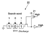
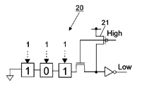
- FIG. FIG. 2 is a circuit diagram of a NAND-type BCAM cell 30 (BCAM cell is also referred to as a word circuit).
- the NAND type word circuit 30 is configured using pass transistors 33 connected in series in a NAND type cell.
- the NAND type word circuit 30 operates in two phases of a precharge phase (precharge) and an evaluation phase (evaluate) by dynamic logic.
- ML also called a match line
- P-type MOS transistor 33e is charged via the P-type MOS transistor 33e.
- the search word is the same as the stored word as shown in FIG. 6, all the pass transistors 21 in the CAM cell are on.
- the CAM cell is a memory cell shown in FIG. Therefore, the capacity of the ML line is discharged. This state is called “match”.
- the search word is simplified to “101” and 3 bits.
- the NAND word circuit 20 consumes less power than the NOR word circuit.
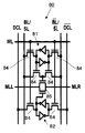
- the binary NAND type BCAM cell 30 includes a flip-flop 32 and first to fifth transmission transistors 33 (33a to 33e).
- the transmission transistor is also called a transfer transistor.
- the BCAM cell 30 is provided with ML, SL, and WL (abbreviated as Word Line, also referred to as word line).
- An ML signal is applied to the ML.
- the SL signal is applied to SL.
- a WL signal is applied to WL.
- WL is activated only when a word is written to a cell, and is held at a low level in the search operation.
- all word inputs are stored by BL and BL bar signals, which are complementary signals applied to the bit lines.
- Data “0” and “1” correspond to (0, 1) and (1, 0), respectively.
- search words are assigned to SL, which is a complementary signal applied to SL, and to the SL bar signal.
- the pass transistor 33e connected to the ML is turned on.
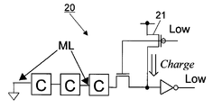
- FIG. 9 is a block diagram of the word circuit 40 by autonomous control based on the phase overlap processing (POP) of the present invention. Only three word circuits 40 are shown. As shown in FIG. 9, each word circuit 40 is controlled by an asynchronous and independent local control signal (lctrl).
- the local control signal (lctrl) is at a high level in the evaluation phase (evaluate) and is at a low level in the precharge phase (precharge).
- the word circuit 40 of the present invention only the ML of the matched word circuit 40 is charged by the local control signal (lctrl) after the previous evaluation phase (evaluate). Since the other local control signals (lctrl) are at the high level, the other word circuits 40 are still in the evaluation phase.
- WOS abbreviation of Word Overlapped Search
- subsequent search words are assigned to other word circuits 40 that are not used. Since the other word circuits 40 that are not used are already charged, the input search word is processed without using the precharge time.
- FIG. 10 is a time chart for explaining the operation of the word circuit 40 by the autonomous control of FIG.
- the ML of the matched word is charged by the local control signal (lctrl).
- the local control signal (lctrl)
- other search words are not used but are assigned to other word circuits 40 in the evaluation phase. Since these phases are carried out in duplicate, delay time of the pre-charging phase T PA does not affect the cycle time T CA.
- the autonomous control based on the POP operation serves to hide the delay time T PA of the pre-charging phase.
- delay time T SA of the evaluation phase longer than the delay time of the pre-charging phase T PA. Therefore, the cycle time T CA is given by the following equation (6).
- phase overlap processing (POP) based on autonomous control in the word block 4 of the CAM block 2 may be a conventional synchronous type.
- FIG. 11 is a block diagram of the synchronous word circuit 42
- FIG. 12 is a time chart for explaining the operation of FIG.
- a clock signal that is a global control signal is applied to the gate of each charging transistor 21.
- a high level clock signal is applied in the evaluation phase
- a low level clock signal is applied in the precharge phase. Therefore, the CAM cycle time (T CS ) in which the word circuit 42 is a synchronous type is given by the following equation (7).
- T SS is the search time given by equation (5), that is, the delay time of the evaluation phase
- T PS is the delay time of the precharge phase.
- T SS is longer than T PS , and these delay times are the same in the synchronous CAM. Therefore, the equation (7) is expressed by the following equation (8).
- the duty ratio of the clock signal in the synchronous circuit is 50%.
- the clock cycle is in the evaluation phase period as shown in equation (8). Twice as much.
- the throughput ratio of the semiconductor memory device 1 of the present invention to the conventional synchronous CAM is given by the following equation (9).
- the delay time T SA of the evaluation phase is approximately equal to T 1st .
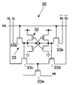
- FIG. 13 is a circuit diagram showing a word circuit 50 including WOS and POP.
- the word circuit 50 of the present invention includes an 8-bit first stage subword circuit 54a, a segmentation circuit 55, an autonomous precharge circuit 56, and a 136 bit second stage subword circuit 54b. It is configured to include.
- an 8-bit first stage subword circuit 54a includes eight NAND cells 58, a P-type MOS transistor 60 for autonomous precharging, a weak feedback P-type MOS transistor 62, It is composed of
- ML is charged by a P-type MOS transistor 60 for autonomous precharging controlled by the autonomous precharging circuit 56.
- the weak feedback P-type MOS transistor 62 is used to solve the problem of ML charge distribution by the NAND cell 58 (see Non-Patent Documents 14, 15, and 24).
- ML1 0 is connected to the autonomous precharge circuit 56 is connected to the second-stage sub-word circuit 54b of 136 bits.
- the 136-bit second-stage subword circuit 54 b includes 17 local match circuits 70 and a global match circuit 72.
- a match circuit is a circuit that determines a match between a word to be searched and a stored word.
- a circuit that performs this operation is a coincidence circuit.
- Such a hierarchical design divides the word circuit 50 into a local match circuit 70 and a global match circuit 72 (see Non-Patent Document 25).
- each local match circuit 70 includes an inverter 71, a P-type MOS transistor 60 for autonomous precharging, a weak feedback P-type MOS transistor 62, and eight NAND cells (sub-cells). - a subword circuit) 58, an output ML1 0 segmentation circuit 55 is composed of N-type MOS transistor 74. issued enter the gate. Once ML1 0 is asserted, that is effective, with 17 local matching circuit 70 operates. In other cases, since the 8-bit first stage subword circuit 54a does not match, the 17 local match circuits 70 do not operate.
- the remaining 136-bit subword 54b is sent in parallel from the input control unit 3, and is divided into 17 sub-subwords by 8 bits. Each sub-subword is processed by the local match circuit 70.
- the output (LMLi 0 (0 ⁇ i ⁇ 17)) of the local match circuit 70 is at a high level when the input sub-subwords match, and is at the low level when the input sub-subwords do not match. .
- the delay time from ML1 0 to LMLi 0 is defined by T 2ndL .
- the global match circuit 72 includes 17 N-type MOS transistors 74 connected in series, a P-type MOS transistor 60 for autonomous precharging, and a weak feedback P-type MOS transistor 62. And an inverter 71.
- the outputs of LMLi 0 are input to the gates of 17 series-connected N-type MOS transistors 74 of the global match circuit 72.
- the output ML2 0 global matching circuit 72 is enabled, i.e. high level is outputted. This state means that the search word matches the stored word. In other states, ML2 0 is at a low level.
- T 2ndG Delay time until a transition from LMLi 0 to ML2 0 is defined by T 2ndG. From this, the delay time T 2nd in the second-stage segment 54b is given by the following equation (11).
- the autonomous precharge circuit 56 shown in FIG. 13C is also operating. As shown in FIG. 13C, the autonomous precharge circuit 56 is a circuit in which AND gates 78 are connected in series. When ML1 0 is asserted, ie, enabled, a delay time T delay is defined.
- the output of the autonomous precharge circuit 56 becomes invalid after the delay time T delay . Then, the autonomous precharge circuit 56 charges all MLs of the word circuit 50.
- FIG. 14 is a time chart showing the operation of the word circuit 50 of FIG.
- the search word is divided into 8-bit sub-word and 136-bit sub-word, it is sent from the input control unit 3 at a rate based on the period of T CA.
- the 8-bit subword 54a matches in the first segment, the remaining 136-bit subword 54b is processed later.
- Search word since changes based on the period of T CA, is the 136-bit word is required to be assigned, that is effective in the local matching circuit 70 within the T CA. For this reason, the delay time of the local matching circuit 70 needs to satisfy the condition of the following equation (12).
- the global match circuit 72 determines whether or not the search words match. At the same time, the autonomous precharge circuit 56 operates.
- the delay time T delay needs to satisfy the condition of the following equation (13).
- T slow needs to satisfy the condition of the following formula (14).
- T prec is a delay time of precharging of all MLs.
- the cycle time T CA shown in FIGS. 10 and 14 is approximately T 1st .
- the 256 ⁇ 144-bit semiconductor memory device 1, 1A of the present invention will be described.
- the 256 ⁇ 144-bit semiconductor memory device 1 or 1A of the present invention is compared with a conventional synchronous CAM using the segment method.
- the bit number (nk) of the second-stage subword is 136 bits.
- the semiconductor memory devices 1 and 1A of the present invention have the same word configuration.
- the configuration of the second-stage subword in the semiconductor memory devices 1 and 1A of the present invention is hierarchical (see Non-Patent Document 25 for hierarchical subwords).
- the semiconductor memory devices 1 and 1A of the present invention and the comparative example have been evaluated based on 90 nm CMOS technology.
- the words to be stored have a uniform random number distribution.
- 90 nm is the minimum processing dimension of the CMOS manufacturing process used.
- Table 1 is a table showing the delay time of each circuit of the semiconductor memory device 1 of the present invention.
- the semiconductor memory device 1 of the present invention was evaluated using HSPICE (SPICE (Simulation Program with Integrated Circuit Emphasis) manufactured by Synopsys) as software.
- the autonomous precharge circuit 56 was designed to satisfy the expression (13).
- m was set to 3.
- T reg is 51ps
- T 1st is 259ps
- T 2ndL is 225ps
- T 2ndG is 243ps
- T delay is 500 ps
- T prec is 81 ps.
- FIG. 15 is a timing chart showing simulation results for the semiconductor memory devices 1 and 1A in the 90 nm CMOS process of the present invention. As shown in FIG. 15, search word followed by a so allocated to different word circuit without using the semiconductor memory device 1,1A of the present invention operates at T CA based on short cycle delay.
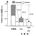
- FIG. 16 is a diagram comparing the cycle times of the CAMs of the semiconductor memory devices 1 and 1A that are autonomously controlled according to the present invention and the comparative example.
- the CAM cycle time of the comparative example is determined by equation (7) and is 1454 ps.
- the cycle time of the semiconductor memory device 1 using the WOS of the present invention operates with the delay time of the first-stage subword circuit. Therefore, the cycle time of the semiconductor memory device 1 using the WOS of the present invention is 555 ps, which is 64.1% lower than that of the conventional CAM.
- the cycle time of the semiconductor memory device 1A using the WOS and POP of the present invention is reduced by 82% as compared with the conventional CAM because the influence of the precharge delay time is eliminated, and the cycle time is about 261 ps. To do.
- the power consumption of the semiconductor memory devices 1 and 1A is given by the following (16).
- E match , E search , and E ctrl are the power consumption of the ML, SL, and control signals, respectively.
- the local match circuit 70 does not operate. Furthermore, the global match circuit 72 operates only when each sub-subword matches the local match circuit 70. Therefore, the power consumption of ML is given by the following equation (17).
- E 1st, E 2ndL, E 2ndG each first-stage sub-word circuit 54a, the local matching circuit 70, a power consumption of global matching circuit 72.
- ML switching probability is very low and SL changes when a new search word is assigned.
- Ectrl which is the power consumption of the control signal, is related to the clock signal, which is a global control signal, in the conventional synchronous CAM.
- the clock signal turns on all P-type MOS transistors 60 for autonomous precharging (see FIG. 10). For this reason, Ectrl (sync) , which is the power consumption of the conventional synchronous CAM control signal, is given by the following equation (18).
- E clk_ buffer
- E prec the power consumption of all the P-type MOS transistors 60 for autonomous precharging.
- the power consumption Ectrl (self) of the input signal of the semiconductor memory device 1A of the present invention is related to the local control signal (lctrl) of the semiconductor memory device 1A by autonomous control. Since only the precharge transistor in the matched word circuit is turned on by the prec signal (precharge signal), the power consumption for charging the precharge P-type MOSFET 60 is reduced. Further, the precharge circuit 56 operates only when the first-stage segments match. For this reason, Ectrl (self) which is the power consumption of the control signal of the semiconductor memory device 1A of the present invention is given by the following equation (19).
- E self_precharge is the power consumption of the precharge circuit.
- Table 2 is a table comparing the power consumption of the semiconductor memory device 1A of the present invention and the CAM of the comparative example. The average cycle time and the number of transistors used are also shown. The average cycle time of the semiconductor memory device 1A of the present invention is 261 ps, and the average cycle time of the synchronous CAM of the comparative example is 1454 ps. From this, it can be seen that the throughput of the semiconductor memory device 1A of the present invention is 5.57 times the CAM of the comparative example.
- the semiconductor memory device 1A of the present invention uses the local control signal (lctrl) and the power consumption of the control signal is reduced, the total power consumption is reduced to 61.6% of the synchronous CAM of the comparative example. .
- the word circuit is locally controlled, an autonomous precharge control circuit is required. For this reason, the area of the CAM of the present invention is very small but increases by 8%.
- the number of transistors of the semiconductor memory device 1A of the present invention is 408k (408,000), and the number of transistors of the synchronous CAM of the comparative example is 372k (372,000).
- Table 3 is a table comparing the semiconductor memory device 1A of the present invention with a conventional example.
- the advantages of the hybrid type are low power consumption and high-speed operation, which depend on the NAND type cell and the NOR type cell, respectively.
- the cycle time was shortened to 8% and the energy consumption / bit per search was reduced to 23% as compared with the hybrid type CAM having a minimum processing dimension of 0.1 ⁇ m.
- the semiconductor memory device 1A according to the present invention operates at a speed about three times that of a NAND CAM having a minimum processing dimension of 65 nm.
- FIG. 17 is a circuit diagram of the TCAM 80.
- the TCAM 80 has a configuration in which two BCAM memory cells 30 shown in FIG. 8 are arranged in parallel to the match line (ML).
- the TCAM 80 includes a NAND first memory cell 81 that stores upper “0” and “1”, a NAND second memory cell 82 that stores lower “X”, and a plurality of transmissions. For example, and an ML transmission transistor 85.
- WL, BL / SL, and BL bar / SL bar are connected to the NAND-type first memory cell 81.
- WL, DCL (don't care line), and DCL bar are connected to the NAND type second memory cell 82.
- the ML is connected to the NAND-type first memory cell 81 and the NAND-type second memory cell 82 through the ML transmission transistor 85.
- the CAM block 2 of the semiconductor memory device 1 and 1A shown in FIG. 1 is the TCAM 80 shown as an example in FIG. 17, and the input control unit 3 and the like are changed from binary to ternary data.
- 1A operates as an associative memory of ternary data.
Abstract
Description
入力制御部は、好ましくは、高速モード及び低速モードで動作する。入力制御部は、好ましくは、kビットの第1段サブワードが検索するワードと一致しないと判定した場合には、異なる入力に対して連続的に一致動作を続けるように高速モードで動作する。入力制御部は、好ましくは、kビットの第1段サブワードが検索するワードと一致したと判定した場合には、検索が連想メモリブロックで完了するまで待機する低速モードで動作する。
連想メモリブロックの検索において、好ましくは、各ワード回路は次の検索を行う前にマッチ線が充電され、該ワード回路内において一致したマッチ線だけが、ワード回路内で生成された局所的制御信号により充電される。
連想メモリブロックの検索において、好ましくは、各ワード回路は次の検索を行う前にマッチ線が充電され、該ワード回路のグローバル一致回路の動作の後でワード回路のマッチ線が充電される。 In the above configuration, the second stage sub-word circuit preferably comprises a further divided sub-sub word circuit, a local match circuit connected to each of the sub-sub word circuits, and a global match circuit of the entire sub-sub word circuit. . The sub-subword circuit is preferably k bits.
The input controller preferably operates in a high speed mode and a low speed mode. The input control unit preferably operates in the high-speed mode so as to continue the matching operation continuously with respect to different inputs when it is determined that the k-bit first stage subword does not match the searched word. The input control unit preferably operates in a low-speed mode that waits until the search is completed in the associative memory block when it is determined that the k-bit first-stage subword matches the word to be searched.
In the search for the associative memory block, preferably, each word circuit is charged with a match line before performing the next search, and only the matched match line in the word circuit is a local control signal generated in the word circuit. Is charged.
In the search for the associative memory block, preferably, each word circuit is charged with the match line before performing the next search, and the match line of the word circuit is charged after the operation of the global match circuit of the word circuit.
入力制御部は、好ましくは、同期信号又は非同期信号により駆動される。
連想メモリブロックは、好ましくは、2値の連想メモリセル又は3値の連想メモリセルからなる。
ワード回路は、好ましくは、自律事前充電回路を含んで構成されている。
一致回路を、好ましくは、ワード毎に非同期で制御し、検索するワードと記憶されているワードの一致を判定する一致操作の後で、一致したワードのマッチラインを、局所的制御信号により自律事前充電し、自律事前充電における遅延時間TPAを、連想メモリブロックのサイクルタイムTCAに影響しないように動作させる。 In the above configuration, the matching circuit is preferably controlled asynchronously or synchronously for each word.
The input control unit is preferably driven by a synchronous signal or an asynchronous signal.
The associative memory block is preferably composed of a binary associative memory cell or a ternary associative memory cell.
The word circuit is preferably configured to include an autonomous precharge circuit.
The match circuit is preferably controlled asynchronously for each word, and after a match operation that determines the match between the word to be searched and the stored word, the match line of the matched word is autonomously pre-adjusted by a local control signal. charging, the delay time T PA in autonomous precharged to operate so as not to affect the cycle time T CA of the associative memory block.
2:CAMブロック
3:入力制御部
4:ワードブロック
4a:kビットのサブワード
4b:(n-k)ビットのサブワード
5、55:セグメント化回路
12、13、14:レジスタ
16:コンパレータ
18:モード制御部
20:ワード回路
21:パストランジスタ
30:BCAMセル
32:フリップフロップ
33、84:伝送用トランジスタ
40:自律制御によるワード回路
42:同期型のワード回路
50:WOSとPOPとを含んだワード回路
54a:8ビットの第1段サブワード回路
54b:136ビットの第2段サブワード回路
56:自律事前充電回路
58:NANDセル(サブ-サブワード回路)
60、76:自律事前充電用のP型MOSトランジスタ
62:弱いフィードバック用P型MOSトランジスタ
70:ローカル一致回路
71:インバータ
72:グローバル一致回路
74:N型MOSトランジスタ
78:ANDゲート
80:TCAM
81:NAND型の第1のメモリセル
82:NAND型の第2のメモリセル
85:ML用伝送用トランジスタ 1, 1A: Semiconductor memory device 2: CAM block 3: Input control unit 4:
60, 76: P-type MOS transistor for autonomous precharging 62: P-type MOS transistor for weak feedback 70: Local match circuit 71: Inverter 72: Global match circuit 74: N-type MOS transistor 78: AND gate 80: TCAM
81: NAND-type first memory cell 82: NAND-type second memory cell 85: ML transmission transistor
(ワード重畳型検索)
図1は、本発明のワード重畳型検索(Word Overlapped Search、以下、WOS方法と略称する。)を用いた半導体記憶装置1の構成を示すブロック図である。
図1に示すように、本発明の半導体記憶装置1は、CAMブロック2と入力制御部3を含んで構成されている。本発明の半導体記憶装置1は、連想メモリであり、CAM(Content-Addressable Memoryの略記号)とも呼ばれる。
CAMブロック2は、nビットのワードを記憶する複数のワード(w語)のワードブロック(ワードブロックはワード回路とも呼ぶ。)4を含んでいて、自律制御又は同期制御により動作する。
ワードブロック4は、小さなkビットのサブワード4aとこのkビットのサブワード4aに接続されるセグメント化回路5と、セグメント化回路5の出力側に接続される後段の(n-k)ビットのサブワード4bとから構成されている。つまり、ワードブロック4は、小さなkビットのサブワード4aと後段の大きな(n-k)ビットのサブワード4bとが、セグメント化回路5を介して分割されている。kビットのサブワード4aは、入力制御部3のSL1(サーチライン1)に接続されている。n-kビットのサブワード4bは、入力制御部3のSL2(サーチライン2)に接続されている。 Embodiments of the present invention will be specifically described below with reference to the drawings.
(Word superposition type search)
FIG. 1 is a block diagram showing a configuration of a
As shown in FIG. 1, the
The
The

続くサブワードが同じであることが判明した場合、次の検索は、両方のセグメントにおいて現在の検索が完了したときに実行される。 After the first k-bit search, most unmatched word blocks 4 are not used. In order to increase the throughput, blocks that are not used in the present invention are used. In the
If subsequent subwords are found to be the same, the next search is performed when the current search is completed in both segments.

入力制御部3は、レジスタ12~14と、kビットのコンパレータ16と、モード制御部18とを含んで構成されている。コンパレータ16は比較回路や比較器とも呼ばれる。モード制御部18は、高速及び低速の二つのモードで動作する。入力制御部3は、同期回路方式で設計されている。この方法は、検索ワードをCAMブロック2中で検索する前に処理するので、事前計算法に分類される(非特許文献20、21)。 FIG. 2 is a block diagram showing the configuration of the
The
最初に、D11がkビットの第1のセグメント(ML10)に一致し、一致した結果はセグメント化回路5に記憶(ストア)される。
2番目に、D21がn-kビットのサブワード4bがkビットの後のセグメント(ML20)に一致する。同時に、D12が別の最初のセグメント(ML10)中で処理される。連続したサブワードD1が異なる場合、この別の最初のセグメントは、一つ前の一致動作の際に不一致と判定されているため、ワード回路の内部状態がそのまま保持されている。一致動作とは、検索するワードと記憶されているワードの一致を判定する操作である。この操作を行う回路が一致回路である。このため、異なる入力に対して連続的に一致動作を続けることが可能となる。連続したD1が同じ場合には、入力制御部3は低速モードで動作する。 FIG. 3 is a time chart of the
First, D1 1 matches the first segment (ML1 0 ) of k bits, and the matching result is stored (stored) in the
Secondly,


一方、従来の同期型のCAMでは、次の検索ワードは、現在の検索が完了した後で割り当てられる。従って、従来の同期型のCAMの検索時間(TSS)は、下記(5)式で与えられる。 (Conventional CAM)
On the other hand, in the conventional synchronous CAM, the next search word is assigned after the current search is completed. Accordingly, the search time (T SS ) of the conventional synchronous CAM is given by the following equation (5).

例えば、ワード検索を2段階に分割し、1段目の検索では先頭の数ビットのみのワード検索を行う。半導体記憶装置1では先頭の数ビットのワード検索で大部分のワード回路4を不一致と判断することができるため、大部分の2段目の長いワード回路4は使用されず、内部状態が保持されているため、続けて次のワード検索を実行できる。この使用されていないワード回路4に入力データをアサイン、つまり実行する制御回路を半導体記憶装置1の入力制御部3に組み込むことで、半導体記憶装置1は1段目の検索終了後に次のデータのワード検索を開始することができる。 The operation of the
For example, the word search is divided into two stages, and the word search of only the first few bits is performed in the first stage search. In the
次に、半導体記憶装置1のワードブロック4中の自律制御に基づく位相オーバラップ処理(Phase Overlapped Processing、以下、POPと略称する。)について説明する。
図5~8は、NAND型セルのワード回路20のブロック図を示し、図5はプリチャージのブロック図、図6は一致の場合のブロック図、図7は不一致の場合のブロック図、図8は、NAND型のBCAMセル(BCAMセルをワード回路とも言う。)30の回路図である。
図8に示すように、NAND型のワード回路30は、NAND型セル中に直列接続されたパストランジスタ33を使用して構成されている。NAND型のワード回路30は、ダイナミック論理により事前充電相(プリチャージ)及び評価相(エバリュエイト)という二つの相で動作する。事前充電相では、ML(マッチ線とも呼ぶ。)はP型MOSトランジスタ33eを介して充電される。 (Phase overlap processing)
Next, phase overlap processing (hereinafter abbreviated as POP) based on autonomous control in the
5 to 8 show block diagrams of the
As shown in FIG. 8, the NAND
図9に示すように、各ワード回路40は、非同期で独立の局所的制御信号(lctrl)により制御される。局所的制御信号(lctrl)は、評価相(エバリュエイト)ではハイレベルであり、事前充電相(プリチャージ)ではローレベルである。 FIG. 9 is a block diagram of the
As shown in FIG. 9, each
図10に示すように、一致操作の後で、一致したワードのMLは、局所的制御信号(lctrl)により充電される。この事前充電相の間において、他の検索ワードは使用していないで評価相の状態にある他のワード回路40に割り当てられる。これらの相は重複して行われるので、事前充電相の遅延時間TPAは、サイクルタイムTCAに影響しない。このように、POP動作に基づく自律制御は、事前充電相の遅延時間TPAを隠蔽するように働く。通常、評価相の遅延時間TSAは、事前充電相の遅延時間TPAよりも長い。
従って、サイクルタイムTCAは、下記(6)式で与えられる。 FIG. 10 is a time chart for explaining the operation of the
As shown in FIG. 10, after the match operation, the ML of the matched word is charged by the local control signal (lctrl). During this precharge phase, other search words are not used but are assigned to
Therefore, the cycle time T CA is given by the following equation (6).

図11は、同期型のワード回路42のブロック図であり、図12は、図11の動作を説明するタイムチャートである。
図11に示すように、ワード回路42を同期型とした場合には、各充電用トランジスタ21のゲートには大局的制御信号であるクロック信号が印加される。具体的には、評価相ではハイレベルのクロック信号が印加され、事前充電相ではローレベルのクロック信号が印加される。
このため、ワード回路42を同期型としたCAMのサイクル時間(TCS)は、下記(7)式で与えられる。 In the
FIG. 11 is a block diagram of the
As shown in FIG. 11, when the
Therefore, the CAM cycle time (T CS ) in which the


図13は、WOSとPOPとを含んだワード回路50を示す回路図である。
図13に示すように、本発明のワード回路50は、8ビットの第1段サブワード回路54aと、セグメント化回路55と、自律事前充電回路56と、136ビットの第2段サブワード回路54bとを含んで構成されている。
図13(a)に示すように、8ビットの第1段サブワード回路54aは、8個のNANDセル58と、自律事前充電用のP型MOSトランジスタ60と、弱いフィードバック用P型MOSトランジスタ62とから構成されている。 Next, a
FIG. 13 is a circuit diagram showing a
As shown in FIG. 13, the
As shown in FIG. 13A, an 8-bit first
図13(d)に示すように、グローバル一致回路72は、17個の直列接続されたN型MOSトランジスタ74と、自律事前充電用のP型MOSトランジスタ60と、弱いフィードバック用P型MOSトランジスタ62と、インバータ71とを含んで構成されている。LMLi0の各出力は、グローバル一致回路72の17個の直列接続されたN型MOSトランジスタ74の各ゲートに入力される。 All outputs of LMLi 0 are connected to the
As shown in FIG. 13D, the

図14に示すように、検索ワードは8ビットのサブワードと136ビットのサブワードに分割され、これらが、TCAという周期に基づく速度で入力制御部3から送出される。8ビットのサブワード54aが第1のセグメント中で一致したとき、残りの136ビットのサブワード54bが後段で処理される。サーチワードは、TCAという周期に基づいて変化するので、136ビットのサブワードはTCAの範囲内でローカル一致回路70にアサイン、つまり有効とされる必要がある。このため、ローカル一致回路70の遅延時間は下記(12)式の条件を満足させる必要がある。 FIG. 14 is a time chart showing the operation of the
As shown in FIG. 14, the search word is divided into 8-bit sub-word and 136-bit sub-word, it is sent from the


上記(3)式、(4)式、(14)式から、比較される後段のサブワード54bの数(m)は下記(15)式で決定される。 Here, T prec is a delay time of precharging of all MLs.
From the above equations (3), (4), and (14), the number (m) of sub-words 54b in the subsequent stage to be compared is determined by the following equation (15).

本発明の256×144ビットの半導体記憶装置1、1Aについて説明する。
本発明の256×144ビットの半導体記憶装置1、1Aを、セグメント法を用いた従来の同期型CAMと比較する。比較例の従来の同期型CAMは、1段目のサブワードのビット数はk=8であり、2段目のサブワードのビット数(n-k)は136ビットである。本発明の半導体記憶装置1、1Aも同じワード構成である。本発明の半導体記憶装置1、1Aにおける2段目のサブワードの構成は、階層型である(階層型のサブワードは非特許文献25参照)。 (256 × 144-bit semiconductor memory device)
The 256 × 144-bit
The 256 × 144-bit
表1は、本発明の半導体記憶装置1の各回路の遅延時間を示す表である。具体的には、本発明の半導体記憶装置1を、ソフトウェアとしてHSPICE(シノプシス社製のSPICE(Simulation Program with Integrated Circuit Emphasis))を用いて評価した。MOSトランジスタのドレイン電圧は、VDD=1Vとし、温度は室温とした。
自律事前充電回路56は、(13)式を満足するように設計した。(15)式を使用して、mを3に設定した。これから、(2)式及び(8)式からTCAが261ps(1ps=10-12s)になった。製造工程の変動により、T2ndはTdelayよりも大きくなる可能性があり、この場合は(13)式を満足しなくなる。しかしながら、(15)式を満足させるために、mを3よりも大きくすることにより対処が可能である。これにより、入力制御部3の面積に影響を与えるが、サイクル時間TCAには直接影響しない。
表1に示すように、Tregは51ps、T1stは259ps、T2ndLは225ps、T2ndGは243ps、Tdelayは500ps、Tprecは81psである。

Table 1 is a table showing the delay time of each circuit of the
The autonomous
As shown in Table 1, T reg is 51ps, T 1st is 259ps, T 2ndL is 225ps, T 2ndG is 243ps, T delay is 500 ps, T prec is 81 ps.
図16は、本発明の自律制御をした半導体記憶装置1、1Aと比較例のCAMのサイクル時間を比較した図である。
図16に示すように、比較例のCAMのサイクル時間は、(7)式で決まり、1454psである。本発明のWOSを用いた半導体記憶装置1のサイクル時間は、1段目のサブワード回路の遅延時間で動作する。このため、本発明のWOSを用いた半導体記憶装置1のサイクル時間は、従来のCAMに比較して64.1%減少し、555psである。 (Cycle time)
FIG. 16 is a diagram comparing the cycle times of the CAMs of the
As shown in FIG. 16, the CAM cycle time of the comparative example is determined by equation (7) and is 1454 ps. The cycle time of the
次に、半導体記憶装置1、1Aの消費電力について説明する。
半導体記憶装置1、1Aの消費電力は下記(16)で与えられる。 (power consumption)
Next, the power consumption of the
The power consumption of the


制御信号の消費電力であるEctrlは、従来の同期式のCAMにおいては、大局的制御信号であるクロック信号に関係している。
クロック信号は、全ての自律事前充電用のP型MOSトランジスタ60をオンにする(図10参照)。このため、従来の同期式のCAMの制御信号の消費電力であるEctrl(sync)は、下記(18)式で与えられる。 (Power consumption of conventional CAM)
Ectrl , which is the power consumption of the control signal, is related to the clock signal, which is a global control signal, in the conventional synchronous CAM.
The clock signal turns on all P-
従来の同期型CAMに対して、本発明の半導体記憶装置1Aの入力信号の消費電力Ectrl(self)は、自律制御による半導体記憶装置1Aの局所的制御信号(lctrl)に関係している。一致したワード回路における事前充電用トランジスタだけがprec信号(事前充電信号)でオンするので、事前充電用のP型MOSFET60を充電する消費電力が低減する。さらに、事前充電回路56は1段目のセグメントが一致したときだけ動作する。このため、本発明の半導体記憶装置1Aの制御信号の消費電力であるEctrl(self)は、下記(19)式で与えられる。 (Power consumption of the semiconductor memory device of the present invention)
In contrast to the conventional synchronous CAM, the power consumption Ectrl (self) of the input signal of the

表2は、本発明の半導体記憶装置1Aと比較例のCAMの消費電力を比較した表である。平均サイクル時間及び使用トランジスタ数も一緒に示している。
本発明の半導体記憶装置1Aの平均サイクル時間は261psであり、比較例の同期型CAMの平均サイクル時間は1454psである。これから、本発明の半導体記憶装置1Aのスループットは、比較例のCAMの5.57倍であることが分かる。

Table 2 is a table comparing the power consumption of the
The average cycle time of the
ハイブリッド型の利点は、低消費電力と高速動作であり、それぞれNAND型のセルとNOR型のセルによる。
本発明の半導体記憶装置1Aは、最小加工寸法が0.1μmのハイブリッド型CAMに比較すると、サイクルタイムは8%に短縮され、1検索当たりの消費エネルギー/ビットは23%に減少した。さらに、本発明の半導体記憶装置1Aは、最小加工寸法が65nmのNAND型CAMに比較すると、約3倍の速度で動作する。

The advantages of the hybrid type are low power consumption and high-speed operation, which depend on the NAND type cell and the NOR type cell, respectively.
In the
次に、本発明の半導体記憶装置1、1Aのメモリセルを、3値を記憶させるTCAMとした場合について説明する。
TCAMでは、「0」、「1」、「X」というように3つの状態を扱う。「X」は、「ドントケア(Don't care)」とも呼ばれている。
図17は、TCAM80の回路図である。
図17に示すように、TCAM80は、図8に示すBCAMのメモリセル30をマッチ線(ML)に対して2つ並列にした構成を有している。つまり、TCAM80は、上段の「0」、「1」を記憶させるNAND型の第1のメモリセル81と、下段の「X」を記憶させるNAND型の第2のメモリセル82と、複数の伝送用トランジスタ84と、ML用伝送用トランジスタ85とを含んで構成されている。NAND型の第1のメモリセル81には、WLと、BL/SLと、BLバー/SLバーと、が接続される。NAND型の第2のメモリセル82には、WLとDCL(ドントケアライン)とDCLバーとが接続される。MLは、ML用伝送用トランジスタ85を介して、NAND型の第1のメモリセル81と、NAND型の第2のメモリセル82に接続される。 (Modification)
Next, the case where the memory cell of the
TCAM handles three states such as “0”, “1”, and “X”. “X” is also called “Don't care”.
FIG. 17 is a circuit diagram of the
As shown in FIG. 17, the
Claims (14)
- レジスタとコンパレータとモード制御部とを含んで構成される入力制御部と、該入力制御部に接続される連想メモリブロックと、
を含み、
上記連想メモリブロックの各ワード回路は、上記入力制御部のサーチライン1に接続されるkビットの第1段サブワード回路と、上記入力制御部のサーチライン2に接続されるn-kビットの第2段サブワード回路と、からなり、
上記kビットの第1段サブワード回路と上記n-kビットの第2段サブワード回路とは、セグメント化回路を介して接続されている、半導体記憶装置。 An input control unit configured to include a register, a comparator, and a mode control unit; an associative memory block connected to the input control unit;
Including
Each word circuit of the associative memory block includes a k-bit first stage sub-word circuit connected to the search line 1 of the input control unit and an nk bit of the nk bit connected to the search line 2 of the input control unit. A two-stage subword circuit,
The semiconductor memory device, wherein the k-bit first-stage subword circuit and the n−k-bit second-stage subword circuit are connected via a segmentation circuit. - 前記第2段サブワード回路は、さらに分割されたサブ-サブワード回路と各該サブ-サブワード回路に接続されるローカル一致回路と、該サブ-サブワード回路全体のグローバル一致回路とからなる、請求項1に記載の半導体記憶装置。 The second stage sub-word circuit comprises a further sub-sub word circuit, a local match circuit connected to each of the sub-sub word circuits, and a global match circuit of the entire sub-sub word circuit. The semiconductor memory device described.
- 前記サブ-サブワード回路はkビットである、請求項2に記載の半導体記憶装置。 3. The semiconductor memory device according to claim 2, wherein said sub-subword circuit is k bits.
- 前記入力制御部は、高速モード及び低速モードで動作する、請求項1~3の何れかに記載の半導体記憶装置。 4. The semiconductor memory device according to claim 1, wherein the input control unit operates in a high speed mode and a low speed mode.
- 前記入力制御部は、前記kビットの第1段サブワードが検索ワードと一致しないと判定した場合には、異なる入力に対して連続的に一致動作を続けるように前記高速モードで動作する、請求項4に記載の半導体記憶装置。 The input control unit operates in the high-speed mode so as to continuously perform a matching operation for different inputs when it is determined that the first bit sub-word of k bits does not match a search word. 5. The semiconductor memory device according to 4.
- 前記入力制御部は、前記kビットの第1段サブワードが検索ワードと一致すると判定した場合には、前記低速モードで動作する、請求項4又は5に記載の半導体記憶装置。 6. The semiconductor memory device according to claim 4, wherein the input control unit operates in the low-speed mode when it is determined that the k-bit first-stage subword matches a search word.
- 前記連想メモリブロックの検索において、各ワード回路は次の検索を行う前にマッチ線が充電され、該ワード回路内において一致したマッチ線だけが、該ワード回路内で生成された局所的制御信号により充電される、請求項1~6の何れかに記載の半導体記憶装置。 In the search for the associative memory block, each word circuit is charged with a match line before performing the next search, and only a match line matched in the word circuit is determined by a local control signal generated in the word circuit. The semiconductor memory device according to claim 1, wherein the semiconductor memory device is charged.
- 前記連想メモリブロックの検索において、各ワード回路は次の検索を行う前にマッチ線が充電され、該ワード回路のグローバル一致回路の動作の後で該ワード回路のマッチ線が充電される、請求項1~6の何れかに記載の半導体記憶装置。
In the search for the associative memory block, each word circuit is charged with a match line before performing a next search, and the match line of the word circuit is charged after the operation of the global match circuit of the word circuit. 7. A semiconductor memory device according to any one of 1 to 6.
- 前記一致回路は、ワード毎に非同期又は同期して制御されることを特徴とする、請求項2に記載の半導体記憶装置。 3. The semiconductor memory device according to claim 2, wherein the matching circuit is controlled asynchronously or synchronously for each word.
- 前記入力制御部は、同期信号又は非同期信号により駆動されることを特徴とする、請求項1~8の何れかに記載の半導体記憶装置。 9. The semiconductor memory device according to claim 1, wherein the input control unit is driven by a synchronous signal or an asynchronous signal.
- 前記連想メモリブロックは、2値の連想メモリセルからなることを特徴とする、請求項1に記載の半導体記憶装置。 2. The semiconductor memory device according to claim 1, wherein the associative memory block includes binary associative memory cells.
- 前記連想メモリブロックは、3値の連想メモリセルからなることを特徴とする、請求項1に記載の半導体記憶装置。 2. The semiconductor memory device according to claim 1, wherein the associative memory block includes ternary associative memory cells.
- 前記ワード回路は、自律事前充電回路を含んで構成されていることを特徴とする、請求項7又は8に記載の半導体記憶装置。 9. The semiconductor memory device according to claim 7, wherein the word circuit includes an autonomous precharge circuit.
- 前記一致回路を、ワード毎に非同期で制御し、
検索するワードと記憶されているワードの一致を判定する一致操作の後で、一致したワードのマッチラインを、局所的制御信号により自律事前充電し、該自律事前充電における遅延時間TPAを、前記連想メモリブロックのサイクルタイムTCAに影響しないように動作させる、請求項9に記載の半導体記憶装置。 Controlling the coincidence circuit asynchronously for each word;
After a match operation for determining a match between a word to be searched and a stored word, the match line of the matched word is autonomously precharged by a local control signal, and the delay time T PA in the autonomous precharge is It is operated so as not to affect the cycle time T CA of the associative memory block, the semiconductor memory device according to claim 9.
Priority Applications (2)
| Application Number | Priority Date | Filing Date | Title |
|---|---|---|---|
| KR1020147034459A KR101948126B1 (en) | 2012-05-06 | 2013-05-03 | Semiconductor storage device |
| US14/399,041 US9324429B2 (en) | 2012-05-06 | 2013-05-03 | Semiconductor storage device |
Applications Claiming Priority (2)
| Application Number | Priority Date | Filing Date | Title |
|---|---|---|---|
| JP2012-105558 | 2012-05-06 | ||
| JP2012105558A JP5998381B2 (en) | 2012-05-06 | 2012-05-06 | Semiconductor memory device |
Publications (1)
| Publication Number | Publication Date |
|---|---|
| WO2013168685A1 true WO2013168685A1 (en) | 2013-11-14 |
Family
ID=49550722
Family Applications (1)
| Application Number | Title | Priority Date | Filing Date |
|---|---|---|---|
| PCT/JP2013/062791 WO2013168685A1 (en) | 2012-05-06 | 2013-05-03 | Semiconductor storage device |
Country Status (4)
| Country | Link |
|---|---|
| US (1) | US9324429B2 (en) |
| JP (1) | JP5998381B2 (en) |
| KR (1) | KR101948126B1 (en) |
| WO (1) | WO2013168685A1 (en) |
Cited By (1)
| Publication number | Priority date | Publication date | Assignee | Title |
|---|---|---|---|---|
| JP2015523670A (en) * | 2012-05-29 | 2015-08-13 | インターナショナル・ビジネス・マシーンズ・コーポレーションInternational Business Machines Corporation | System and method for retrieving content addressable memory (CAM) |
Families Citing this family (2)
| Publication number | Priority date | Publication date | Assignee | Title |
|---|---|---|---|---|
| KR101714984B1 (en) * | 2016-08-29 | 2017-03-09 | 인하대학교 산학협력단 | Method and Apparatus for Regionally Self-resetting Circuit |
| TWI713051B (en) * | 2019-10-21 | 2020-12-11 | 瑞昱半導體股份有限公司 | Content addressable memory device |
Citations (5)
| Publication number | Priority date | Publication date | Assignee | Title |
|---|---|---|---|---|
| JPH02308499A (en) * | 1989-05-23 | 1990-12-21 | Toshiba Corp | Content-addressable memory |
| JPH03212896A (en) * | 1990-01-16 | 1991-09-18 | Mitsubishi Electric Corp | Content-addressable memory |
| JPH06333395A (en) * | 1993-05-19 | 1994-12-02 | Kawasaki Steel Corp | Associative memory |
| JPH0714391A (en) * | 1993-06-22 | 1995-01-17 | Kawasaki Steel Corp | Semiconductor storage device |
| JP2013037750A (en) * | 2011-08-10 | 2013-02-21 | Renesas Electronics Corp | Contents reference memory |
Family Cites Families (7)
| Publication number | Priority date | Publication date | Assignee | Title |
|---|---|---|---|---|
| US3997882A (en) | 1975-04-01 | 1976-12-14 | Burroughs Corporation | Content addressable memory system employing charge coupled device storage and directory registers and N/(1-H) counter refresh synchronization |
| US5485418A (en) | 1990-01-16 | 1996-01-16 | Mitsubishi Denki Kabushiki Kaisha | Associative memory |
| JP2002197873A (en) * | 2000-12-27 | 2002-07-12 | Kawasaki Microelectronics Kk | Associative memory |
| JP2002237190A (en) | 2001-02-07 | 2002-08-23 | Kawasaki Microelectronics Kk | Associative memory device and its constituting method |
| JP4552689B2 (en) | 2005-02-28 | 2010-09-29 | 株式会社日立製作所 | Semiconductor memory device |
| JP4861012B2 (en) * | 2005-03-31 | 2012-01-25 | ルネサスエレクトロニクス株式会社 | CAM equipment |
| US7426127B2 (en) * | 2006-12-21 | 2008-09-16 | Intel Corporation | Full-rail, dual-supply global bitline accelerator CAM circuit |
-
2012
- 2012-05-06 JP JP2012105558A patent/JP5998381B2/en active Active
-
2013
- 2013-05-03 KR KR1020147034459A patent/KR101948126B1/en active IP Right Grant
- 2013-05-03 WO PCT/JP2013/062791 patent/WO2013168685A1/en active Application Filing
- 2013-05-03 US US14/399,041 patent/US9324429B2/en active Active
Patent Citations (5)
| Publication number | Priority date | Publication date | Assignee | Title |
|---|---|---|---|---|
| JPH02308499A (en) * | 1989-05-23 | 1990-12-21 | Toshiba Corp | Content-addressable memory |
| JPH03212896A (en) * | 1990-01-16 | 1991-09-18 | Mitsubishi Electric Corp | Content-addressable memory |
| JPH06333395A (en) * | 1993-05-19 | 1994-12-02 | Kawasaki Steel Corp | Associative memory |
| JPH0714391A (en) * | 1993-06-22 | 1995-01-17 | Kawasaki Steel Corp | Semiconductor storage device |
| JP2013037750A (en) * | 2011-08-10 | 2013-02-21 | Renesas Electronics Corp | Contents reference memory |
Cited By (1)
| Publication number | Priority date | Publication date | Assignee | Title |
|---|---|---|---|---|
| JP2015523670A (en) * | 2012-05-29 | 2015-08-13 | インターナショナル・ビジネス・マシーンズ・コーポレーションInternational Business Machines Corporation | System and method for retrieving content addressable memory (CAM) |
Also Published As
| Publication number | Publication date |
|---|---|
| JP5998381B2 (en) | 2016-09-28 |
| JP2013235620A (en) | 2013-11-21 |
| US20150109842A1 (en) | 2015-04-23 |
| KR20150014487A (en) | 2015-02-06 |
| US9324429B2 (en) | 2016-04-26 |
| KR101948126B1 (en) | 2019-02-14 |
Similar Documents
| Publication | Publication Date | Title |
|---|---|---|
| Onizawa et al. | High-throughput low-energy content-addressable memory based on self-timed overlapped search mechanism | |
| US6392910B1 (en) | Priority encoder with multiple match function for content addressable memories and methods for implementing the same | |
| Imani et al. | ReMAM: Low energy resistive multi-stage associative memory for energy efficient computing | |
| Jarollahi et al. | Algorithm and architecture for a low-power content-addressable memory based on sparse clustered networks | |
| Huan et al. | A low-power accelerator for deep neural networks with enlarged near-zero sparsity | |
| CN1623205A (en) | Circuit and memory for reducing power usage in a content addressable memory | |
| Yang et al. | A low-power ternary content addressable memory with Pai-Sigma matchlines | |
| Mahendra et al. | Energy-efficient precharge-free ternary content addressable memory (TCAM) for high search rate applications | |
| Hussain et al. | Match-line division and control to reduce power dissipation in content addressable memory | |
| Onizawa et al. | High-throughput low-energy self-timed CAM based on reordered overlapped search mechanism | |
| Jarollahi et al. | A low-power content-addressable memory based on clustered-sparse networks | |
| JP5998381B2 (en) | Semiconductor memory device | |
| Imani et al. | CAP: Configurable resistive associative processor for near-data computing | |
| Karthik et al. | Design and Implementation of a Low Power Ternary Content Addressable Memory (TCAM) | |
| US20160358654A1 (en) | Low-power ternary content addressable memory | |
| Onizawa et al. | High-throughput CAM based on a synchronous overlapped search scheme | |
| Devi et al. | Low Energy Asynchronous CAM Based On Reordered Overlapped Search Mechanism | |
| Ali et al. | A comprehensive review of energy efficient content addressable memory circuits for network applications | |
| Jiang et al. | A fully parallel content addressable memory design using multi-bank structure | |
| Alrushood et al. | Improving Energy Consumption in Content-Addressable Memory Through Precomputation | |
| Zackriya et al. | Selective match-line energizer content addressable memory (SMLE-CAM) | |
| Chen et al. | Filter-based dual-voltage architecture for low-power long-word TCAM design | |
| Mahendra et al. | Design and Implementation of Drivers and Selectors for Content Addressable Memory (CAM) | |
| Muthukrishnan et al. | An Efficient Low Power Sparse Clustered Network By Using Reordered Overlapped Content Addressable Memory | |
| KR101049942B1 (en) | Dynamic Serial-Parallel Cam |
Legal Events
| Date | Code | Title | Description |
|---|---|---|---|
| 121 | Ep: the epo has been informed by wipo that ep was designated in this application |
Ref document number: 13787419 Country of ref document: EP Kind code of ref document: A1 |
|
| WWE | Wipo information: entry into national phase |
Ref document number: 14399041 Country of ref document: US |
|
| NENP | Non-entry into the national phase |
Ref country code: DE |
|
| ENP | Entry into the national phase |
Ref document number: 20147034459 Country of ref document: KR Kind code of ref document: A |
|
| 122 | Ep: pct application non-entry in european phase |
Ref document number: 13787419 Country of ref document: EP Kind code of ref document: A1 |