WO2013147276A1 - 縦型高耐圧半導体装置および縦型高耐圧半導体装置の製造方法 - Google Patents
縦型高耐圧半導体装置および縦型高耐圧半導体装置の製造方法 Download PDFInfo
- Publication number
- WO2013147276A1 WO2013147276A1 PCT/JP2013/059777 JP2013059777W WO2013147276A1 WO 2013147276 A1 WO2013147276 A1 WO 2013147276A1 JP 2013059777 W JP2013059777 W JP 2013059777W WO 2013147276 A1 WO2013147276 A1 WO 2013147276A1
- Authority
- WO
- WIPO (PCT)
- Prior art keywords
- layer
- semiconductor
- sic
- conductivity type
- mosfet
- Prior art date
- Legal status (The legal status is an assumption and is not a legal conclusion. Google has not performed a legal analysis and makes no representation as to the accuracy of the status listed.)
- Ceased
Links
Images





Classifications
-
- H—ELECTRICITY
- H10—SEMICONDUCTOR DEVICES; ELECTRIC SOLID-STATE DEVICES NOT OTHERWISE PROVIDED FOR
- H10D—INORGANIC ELECTRIC SEMICONDUCTOR DEVICES
- H10D30/00—Field-effect transistors [FET]
- H10D30/60—Insulated-gate field-effect transistors [IGFET]
- H10D30/64—Double-diffused metal-oxide semiconductor [DMOS] FETs
- H10D30/66—Vertical DMOS [VDMOS] FETs
-
- H—ELECTRICITY
- H10—SEMICONDUCTOR DEVICES; ELECTRIC SOLID-STATE DEVICES NOT OTHERWISE PROVIDED FOR
- H10D—INORGANIC ELECTRIC SEMICONDUCTOR DEVICES
- H10D12/00—Bipolar devices controlled by the field effect, e.g. insulated-gate bipolar transistors [IGBT]
- H10D12/01—Manufacture or treatment
- H10D12/031—Manufacture or treatment of IGBTs
-
- H—ELECTRICITY
- H10—SEMICONDUCTOR DEVICES; ELECTRIC SOLID-STATE DEVICES NOT OTHERWISE PROVIDED FOR
- H10D—INORGANIC ELECTRIC SEMICONDUCTOR DEVICES
- H10D12/00—Bipolar devices controlled by the field effect, e.g. insulated-gate bipolar transistors [IGBT]
- H10D12/01—Manufacture or treatment
- H10D12/031—Manufacture or treatment of IGBTs
- H10D12/032—Manufacture or treatment of IGBTs of vertical IGBTs
-
- H—ELECTRICITY
- H10—SEMICONDUCTOR DEVICES; ELECTRIC SOLID-STATE DEVICES NOT OTHERWISE PROVIDED FOR
- H10D—INORGANIC ELECTRIC SEMICONDUCTOR DEVICES
- H10D12/00—Bipolar devices controlled by the field effect, e.g. insulated-gate bipolar transistors [IGBT]
- H10D12/411—Insulated-gate bipolar transistors [IGBT]
- H10D12/441—Vertical IGBTs
-
- H—ELECTRICITY
- H10—SEMICONDUCTOR DEVICES; ELECTRIC SOLID-STATE DEVICES NOT OTHERWISE PROVIDED FOR
- H10D—INORGANIC ELECTRIC SEMICONDUCTOR DEVICES
- H10D30/00—Field-effect transistors [FET]
- H10D30/60—Insulated-gate field-effect transistors [IGFET]
-
- H—ELECTRICITY
- H10—SEMICONDUCTOR DEVICES; ELECTRIC SOLID-STATE DEVICES NOT OTHERWISE PROVIDED FOR
- H10D—INORGANIC ELECTRIC SEMICONDUCTOR DEVICES
- H10D62/00—Semiconductor bodies, or regions thereof, of devices having potential barriers
- H10D62/10—Shapes, relative sizes or dispositions of the regions of the semiconductor bodies; Shapes of the semiconductor bodies
-
- H—ELECTRICITY
- H10—SEMICONDUCTOR DEVICES; ELECTRIC SOLID-STATE DEVICES NOT OTHERWISE PROVIDED FOR
- H10D—INORGANIC ELECTRIC SEMICONDUCTOR DEVICES
- H10D62/00—Semiconductor bodies, or regions thereof, of devices having potential barriers
- H10D62/10—Shapes, relative sizes or dispositions of the regions of the semiconductor bodies; Shapes of the semiconductor bodies
- H10D62/102—Constructional design considerations for preventing surface leakage or controlling electric field concentration
- H10D62/103—Constructional design considerations for preventing surface leakage or controlling electric field concentration for increasing or controlling the breakdown voltage of reverse-biased devices
- H10D62/105—Constructional design considerations for preventing surface leakage or controlling electric field concentration for increasing or controlling the breakdown voltage of reverse-biased devices by having particular doping profiles, shapes or arrangements of PN junctions; by having supplementary regions, e.g. junction termination extension [JTE]
-
- H—ELECTRICITY
- H10—SEMICONDUCTOR DEVICES; ELECTRIC SOLID-STATE DEVICES NOT OTHERWISE PROVIDED FOR
- H10D—INORGANIC ELECTRIC SEMICONDUCTOR DEVICES
- H10D62/00—Semiconductor bodies, or regions thereof, of devices having potential barriers
- H10D62/10—Shapes, relative sizes or dispositions of the regions of the semiconductor bodies; Shapes of the semiconductor bodies
- H10D62/102—Constructional design considerations for preventing surface leakage or controlling electric field concentration
- H10D62/103—Constructional design considerations for preventing surface leakage or controlling electric field concentration for increasing or controlling the breakdown voltage of reverse-biased devices
- H10D62/105—Constructional design considerations for preventing surface leakage or controlling electric field concentration for increasing or controlling the breakdown voltage of reverse-biased devices by having particular doping profiles, shapes or arrangements of PN junctions; by having supplementary regions, e.g. junction termination extension [JTE]
- H10D62/109—Reduced surface field [RESURF] PN junction structures
- H10D62/111—Multiple RESURF structures, e.g. double RESURF or 3D-RESURF structures
-
- H—ELECTRICITY
- H10—SEMICONDUCTOR DEVICES; ELECTRIC SOLID-STATE DEVICES NOT OTHERWISE PROVIDED FOR
- H10D—INORGANIC ELECTRIC SEMICONDUCTOR DEVICES
- H10D62/00—Semiconductor bodies, or regions thereof, of devices having potential barriers
- H10D62/10—Shapes, relative sizes or dispositions of the regions of the semiconductor bodies; Shapes of the semiconductor bodies
- H10D62/17—Semiconductor regions connected to electrodes not carrying current to be rectified, amplified or switched, e.g. channel regions
- H10D62/393—Body regions of DMOS transistors or IGBTs
-
- H—ELECTRICITY
- H10—SEMICONDUCTOR DEVICES; ELECTRIC SOLID-STATE DEVICES NOT OTHERWISE PROVIDED FOR
- H10D—INORGANIC ELECTRIC SEMICONDUCTOR DEVICES
- H10D62/00—Semiconductor bodies, or regions thereof, of devices having potential barriers
- H10D62/40—Crystalline structures
- H10D62/405—Orientations of crystalline planes
-
- H—ELECTRICITY
- H10—SEMICONDUCTOR DEVICES; ELECTRIC SOLID-STATE DEVICES NOT OTHERWISE PROVIDED FOR
- H10D—INORGANIC ELECTRIC SEMICONDUCTOR DEVICES
- H10D62/00—Semiconductor bodies, or regions thereof, of devices having potential barriers
- H10D62/80—Semiconductor bodies, or regions thereof, of devices having potential barriers characterised by the materials
- H10D62/83—Semiconductor bodies, or regions thereof, of devices having potential barriers characterised by the materials being Group IV materials, e.g. B-doped Si or undoped Ge
- H10D62/832—Semiconductor bodies, or regions thereof, of devices having potential barriers characterised by the materials being Group IV materials, e.g. B-doped Si or undoped Ge being Group IV materials comprising two or more elements, e.g. SiGe
- H10D62/8325—Silicon carbide
-
- H—ELECTRICITY
- H10—SEMICONDUCTOR DEVICES; ELECTRIC SOLID-STATE DEVICES NOT OTHERWISE PROVIDED FOR
- H10P—GENERIC PROCESSES OR APPARATUS FOR THE MANUFACTURE OR TREATMENT OF DEVICES COVERED BY CLASS H10
- H10P30/00—Ion implantation into wafers, substrates or parts of devices
- H10P30/20—Ion implantation into wafers, substrates or parts of devices into semiconductor materials, e.g. for doping
- H10P30/202—Ion implantation into wafers, substrates or parts of devices into semiconductor materials, e.g. for doping characterised by the semiconductor materials
- H10P30/204—Ion implantation into wafers, substrates or parts of devices into semiconductor materials, e.g. for doping characterised by the semiconductor materials into Group IV semiconductors
- H10P30/2042—Ion implantation into wafers, substrates or parts of devices into semiconductor materials, e.g. for doping characterised by the semiconductor materials into Group IV semiconductors into crystalline silicon carbide
-
- H—ELECTRICITY
- H10—SEMICONDUCTOR DEVICES; ELECTRIC SOLID-STATE DEVICES NOT OTHERWISE PROVIDED FOR
- H10P—GENERIC PROCESSES OR APPARATUS FOR THE MANUFACTURE OR TREATMENT OF DEVICES COVERED BY CLASS H10
- H10P30/00—Ion implantation into wafers, substrates or parts of devices
- H10P30/20—Ion implantation into wafers, substrates or parts of devices into semiconductor materials, e.g. for doping
- H10P30/21—Ion implantation into wafers, substrates or parts of devices into semiconductor materials, e.g. for doping of electrically active species
-
- H—ELECTRICITY
- H10—SEMICONDUCTOR DEVICES; ELECTRIC SOLID-STATE DEVICES NOT OTHERWISE PROVIDED FOR
- H10P—GENERIC PROCESSES OR APPARATUS FOR THE MANUFACTURE OR TREATMENT OF DEVICES COVERED BY CLASS H10
- H10P30/00—Ion implantation into wafers, substrates or parts of devices
- H10P30/20—Ion implantation into wafers, substrates or parts of devices into semiconductor materials, e.g. for doping
- H10P30/28—Ion implantation into wafers, substrates or parts of devices into semiconductor materials, e.g. for doping characterised by an annealing step, e.g. for activation of dopants
-
- H—ELECTRICITY
- H10—SEMICONDUCTOR DEVICES; ELECTRIC SOLID-STATE DEVICES NOT OTHERWISE PROVIDED FOR
- H10D—INORGANIC ELECTRIC SEMICONDUCTOR DEVICES
- H10D62/00—Semiconductor bodies, or regions thereof, of devices having potential barriers
- H10D62/10—Shapes, relative sizes or dispositions of the regions of the semiconductor bodies; Shapes of the semiconductor bodies
- H10D62/124—Shapes, relative sizes or dispositions of the regions of semiconductor bodies or of junctions between the regions
- H10D62/126—Top-view geometrical layouts of the regions or the junctions
- H10D62/127—Top-view geometrical layouts of the regions or the junctions of cellular field-effect devices, e.g. multicellular DMOS transistors or IGBTs
Definitions
- the present invention relates to a power semiconductor device capable of controlling a high breakdown voltage and large current, and more particularly to a vertical high breakdown voltage MOSFET device and IGBT using silicon carbide, which is one of wide band gap materials, as a semiconductor.
- a silicon (Si) single crystal has been used as a material of a power semiconductor element (power device) that controls high breakdown voltage and large current.
- power semiconductor elements for example, bipolar transistors and IGBTs (insulated gate bipolar transistors) are difficult to switch at high speed, although they have a high current density.
- a bipolar transistor has a usage limit of a frequency of about several kHz
- an IGBT has a usage limit of a frequency of about 20 kHz.
- a power MOSFET cannot be used for a large current, but can be used at a high speed up to a frequency of about several MHz.
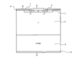
- FIG. 1 is an explanatory view showing a cross-sectional structure of a general MOSFET.
- FIG. 1 shows a cross-sectional structure of a typical (general) MOSFET as a power device capable of handling a large current and having high speed.
- an epitaxially formed low concentration N ⁇ drift layer b is provided on the front surface side of the substrate a.
- a P base layer c is further formed on the surface layer on the front surface side of the low concentration N ⁇ drift layer b.
- a high concentration N + source layer d is selectively formed on the front surface layer of the P base layer c.
- a gate electrode f is formed on the N ⁇ drift layer b, the P base layer c, and the high-concentration N + source layer d via a gate insulating film e.
- a drain electrode g is formed on the back side of the substrate a.
- SiC has attracted particular attention as a next-generation power semiconductor element in recent years because it is an element excellent in low on-voltage, high-speed and high-temperature characteristics (the following non-patent document) See reference 3.)
- SiC is attracting attention as a next-generation power semiconductor element.
- SiC is a chemically very stable material, has a wide band gap of 3 eV, and can be used extremely stably as a semiconductor even at high temperatures. It is done.
- the background of SiC attracting attention as a next-generation power semiconductor element is that the maximum electric field strength is one digit or more larger than Si.
- SiC is likely to exceed the material limit of Si, future growth is expected as a power semiconductor, particularly a MOSFET.
- SiC is expected to have a low on-resistance.
- a vertical SiC-MOSFET having an even lower on-resistance while maintaining high breakdown voltage characteristics can be expected.
- SiC-MOSFET formed in this way is expected to be used as a switching device because it can be switched at high speed with low on-resistance.
- SiC-MOSFETs are expected to be used in power converters such as motor control inverters and uninterruptible power supplies (UPS) as elements capable of high-speed switching with low on-resistance.
- UPS uninterruptible power supplies
- SiC is a wide band gap semiconductor material
- its breakdown electric field strength is as high as about 10 times that of Si as described above, and the on-resistance is expected to be sufficiently small.
- the breakdown electric field strength of the semiconductor becomes about 10 times higher, the load of the electric field on the oxide film particularly when a high voltage is applied becomes larger than that of the Si element. For this reason, since the breakdown electric field strength of Si was reached before a large electric field was applied to the oxide film, it was not a problem with power devices using Si. In power devices using SiC with a very high breakdown electric field strength of semiconductors, Is a problem, and there is a concern that the oxide film will be destroyed first.
- the present invention forms a gate electrode even when a high voltage is applied in a vertical SiC-MOSFET using SiC or the like as a semiconductor material while utilizing its low on-resistance characteristics.
- An object of the present invention is to provide a vertical high-voltage semiconductor device and a method for manufacturing a vertical high-voltage semiconductor device that can exhibit low on-resistance of SiC while improving reliability by preventing the breakdown of an oxide film. .
- a vertical high voltage semiconductor device has the following characteristics.
- a first semiconductor layer (2) of a first conductivity type formed on a first conductivity type semiconductor substrate (1) and having an impurity concentration lower than that of the semiconductor substrate (1) is formed, and the first semiconductor layer
- a second semiconductor layer (3) of the second conductivity type and having a higher impurity concentration than the first semiconductor layer (2) is selectively formed on the surface of (2).
- a base layer (4) of the second conductivity type is provided on the first semiconductor layer (2) and the second semiconductor layer (3), and the first conductivity type is formed on the surface layer of the base layer (4).
- a source region (7) is selectively formed.
- a first conductivity type N-turnback layer (6) is formed so as to penetrate the base layer (4) from the surface and reach the first semiconductor layer (2).
- a gate electrode layer provided on at least a part of the exposed surface of the base layer (4) sandwiched between the source region (7) and the N-turnback layer (6) via a gate insulating film (9) (10), a source electrode (11) in common contact with the surfaces of the source region (7) and the base layer (4), and a drain electrode (12) provided on the back surface of the semiconductor substrate (1) And have.
- a part of said 2nd semiconductor layer (3) is mutually couple
- the vertical high voltage semiconductor device is characterized in that, in the above-described invention, the semiconductor material of the semiconductor substrate (1) is silicon carbide.
- the vertical high-voltage semiconductor device is the above-described invention, wherein the crystallographic plane index of the semiconductor substrate (1) is a plane parallel to (000-1) or a plane tilted within 10 degrees. It is characterized by being.
- the vertical high-voltage semiconductor device is the above-described invention, wherein the crystallographic plane index of the semiconductor substrate (1) is a plane parallel to (0001) or a plane tilted within 10 degrees. It is characterized by.
- a method for manufacturing a vertical high voltage semiconductor device has the following characteristics. First, a step of forming a first semiconductor layer (2) having a first conductivity type and an impurity concentration lower than that of the semiconductor substrate (1) is performed on a first conductivity type semiconductor substrate (1). Next, a second semiconductor layer (3) having a second conductivity type and a higher impurity concentration than the first semiconductor layer (2) is selectively formed on the surface of the first semiconductor layer (2) by an ion implantation method. And a step of forming a second conductivity type base layer (4) on the first semiconductor layer (2) and the second semiconductor layer (3) by an epitaxial growth method.
- a first conductivity type source region (7) selectively formed on the surface layer of the base layer (4), and the first semiconductor layer (2) penetrating the base layer (4) from the surface.
- the step of forming the second semiconductor layer (3) is formed such that parts of the second semiconductor layer (3) are coupled to each other in a region under the N-turn-back layer (6). To do.
- the conductivity type of the substrate is N-type
- a P-type collector layer may be formed on the back surface of the N-type substrate by a technique such as epitaxial growth or ion implantation.
- the high on-voltage characteristic is utilized while utilizing the low on-resistance characteristics. Even at the time of application, the reliability can be improved by preventing the oxide film forming the gate electrode from being broken, and the low on-resistance of SiC can be exhibited.
- FIG. 1 is an explanatory view showing a cross-sectional structure of a general MOSFET.
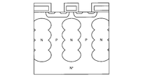
- FIG. 2 is an explanatory view showing a cross-sectional structure of a conventional silicon superjunction MOSFET.
- FIG. 3 is an explanatory view showing a cross-sectional structure (multi-epi method) of a conventional silicon superjunction MOSFET.
- FIG. 4 is an explanatory view showing a cross-sectional structure (trench filling method) of a conventional silicon superjunction MOSFET.
- FIG. 5 is a cross-sectional view in each manufacturing process of the SiC-MOSFET of Example 1, FIG. 5 (a) is a portion where the P + layer is not coupled, and FIG. 5 (b) is a diagram where the P + layer is coupled.
- FIG. FIG. 6 is a plan view showing the arrangement of the P + layer and the cell in the SiC-MOSFET of the first embodiment.
- FIG. 7 is an explanatory diagram showing the connection state of the P + layers of Example 1 as compared with the prior art.
- FIG. 8 is an explanatory diagram showing the results of a comparative characteristic evaluation between the SiC-MOSFET of the example according to the present invention and a conventional SiC-MOSFET in which no P + layer is connected.
- FIG. 9 is an explanatory diagram showing actual measurement results when the device breakdown voltage of the SiC-MOSFET and the width of the N-turnback layer 6 are changed.
- FIG. 10 is an explanatory diagram showing a load short-circuit withstand test result of Example 1.
- FIG. 10 is an explanatory diagram showing a load short-circuit withstand test result of Example 1.
- FIG. 11 is an explanatory diagram showing the evaluation results of turn-off breakdown resistance of the SiC-MOSFET of Example 1.
- FIG. 12 is a plan view showing the arrangement of the P + layer 3 and the cell in the SiC-MOSFET of the third embodiment.
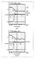
- FIG. 13 is an explanatory diagram showing a turn-off switching waveform of the SiC-MOSFET according to the first embodiment.
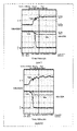
- FIG. 14 is an explanatory diagram showing a turn-on switching waveform of the SiC-MOSFET of the first embodiment.
- FIG. 5 is a cross-sectional view in each manufacturing process of the SiC-MOSFET of Example 1
- FIG. 5 (a) is a portion where the P + layer is not bonded
- FIG. 5 (b) is a P + layer (in the case of IGBT).
- Fig. 2 shows a cross-sectional view of a portion where a P + substrate) is bonded.
- a vertical planar gate MOSFET a silicon carbide (SiC) is used as a semiconductor material, and a MOSFET having an element withstand voltage of 1200 V will be described as an example.
- the SiC-MOSFET of Example 1 uses an N-type SiC semiconductor substrate 1 as a semiconductor substrate.
- the semiconductor substrate according to the present invention can be realized by the low-resistance N-type SiC semiconductor substrate 1 containing about 2 ⁇ 10 19 cm ⁇ 3 of nitrogen as an impurity.
- the SiC-MOSFET of the first embodiment first, for example, nitrogen is added on the surface of the N-type SiC semiconductor substrate 1 with a crystallographic plane index inclined about 4 degrees with respect to (000-1).
- An N-type SiC layer 2 containing about 0.0 ⁇ 10 16 cm ⁇ 3 is epitaxially grown about 10 ⁇ m.
- the first semiconductor layer can be realized by the N-type SiC layer 2 epitaxially grown on the N-type SiC semiconductor substrate 1.
- N-type SiC layer 2 is formed on the front surface side of N-type SiC semiconductor substrate 1.
- a P + layer 3 is formed on the N-type SiC layer (first semiconductor layer) 2 epitaxially grown on the N-type SiC semiconductor substrate 1 by ion implantation.
- the P + layer (second semiconductor layer) 3 has a width of 13 ⁇ m and a depth of 0.5 ⁇ m.
- aluminum is used as ions.
- the dose is set so that the impurity concentration when forming the P + layer 3 is, for example, 1.0 ⁇ 10 18 cm ⁇ 3 .
- FIG. 6 is a plan view showing the arrangement of the P + layer 3 and the cell in the SiC-MOSFET of the first embodiment.
- P + layer 3 under N Uchikaeshi layer 6 to be described later, a part of the P + layer 3, are coupled to each other by a connecting portion 13.
- the P + layer 3 is a portion far from a PN junction between a P base layer 4 and an N return layer 6 described later, and a part of the P + layer 3 is coupled to each other by a connecting portion 13 (see FIG. 6).
- the part of the P + layer 3 that is bonded in the region below the N counter layer 6 is separated from the PN junction formed by the P base layer 4 and the N counter layer 6.
- the distance between the P + layers 3 that are not coupled is 2 ⁇ m.
- the P base layer 4 is formed to have a thickness of 0.5 ⁇ m by an epitaxial growth method.
- aluminum is used as an impurity, and the impurity concentration is set to 2.0 ⁇ 10 16 cm ⁇ 3 .
- the P base layer 4 is of the second conductivity type and has a relatively low impurity concentration. The impurity concentration of the P base layer 4 is set lower than the impurity concentration of the P + layer 3.
- nitrogen ions are selectively implanted into the P base layer 4 as the N repelling layer 6, and the N + source layer (first conductivity type source region) 7 and the P + contact layer 8 are selectively incorporated into the P base layer 4.
- Nitrogen ions are selectively implanted into the P base layer 4 so as to have a depth of 1.5 ⁇ 10 16 cm ⁇ 3 and a depth of 1.5 ⁇ m and a width of 2.0 ⁇ m.
- activation annealing is performed.
- the heat treatment temperature for activation annealing is 1620 ° C.
- the heat treatment time is 2 minutes.
- FIG. 7 is an explanatory diagram showing the connection state of the P + layers of Example 1 as compared with the prior art.
- a region to be ion-implanted when the N + source layer 7 and the P + contact layer 8 are selectively formed in the P base layer 4 as the N return layer 6 is shown in comparison with the conventional technique.
- the P + layers which are hexagonal cells
- FIG. 7B the first embodiment, as shown in FIG. 7B.
- each of the P + layers 3 that are hexagonal cells is coupled to each other with two other P + layers 3 adjacent to each other at each vertex. That is, in Example 1, as shown in FIG. 7B, aluminum ions are implanted as the P + layer 3 using a mask that connects the P + layers 3 to each other.
- a gate insulating film (oxide film) 9 having a thickness of 100 nm is formed by thermal oxidation and annealed in the vicinity of 1000 ° C. in a hydrogen atmosphere. Then, a polycrystalline Si layer doped with phosphorus is formed as a gate electrode 10 and patterned. The gate electrode 10 is provided on at least a part of the exposed surface portion of the P base layer 4 sandwiched between the N + source layer 7 and the N return layer 6 via the gate insulating film 9.
- phosphorous glass is formed to a thickness of 1.0 ⁇ m and patterned, and then heat treatment is performed to form the interlayer insulating film 14. Then, after the interlayer insulating film 14 is formed, aluminum containing 1% Si is formed on the surface with a thickness of 5 ⁇ m by sputtering, and the source electrode 11 is formed.
- a nickel film is formed on the back surface side of the N-type SiC semiconductor substrate 1, heat treatment is performed at 970 ° C., Ti / Ni / Au film is formed, and the drain electrode 12 is formed. Thereafter, the SiC-MOSFET of Example 1 is completed by adding a protective film to the surface.
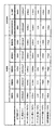
- FIG. 8 is an explanatory diagram showing the results of a comparative characteristic evaluation between the SiC-MOSFET of the example according to the present invention and a conventional SiC-MOSFET in which no P + layer is connected.
- FIG. 8 shows the measurement results of the electrical characteristics of the SiC-MOSFET produced as described above.
- the chip size used for the measurement is 3 mm square, the active area is 5.27 mm 2 , and the rated current is 25A.
- the SiC-MOSFET of Example 1 has a sufficiently low on-resistance (RonA) of 2.80 m ⁇ cm 2 . Further, the SiC-MOSFET of Example 1 has an initial device breakdown voltage of 1450 V, and exhibits sufficiently good characteristics as a 1200 V device.
- the SiC-MOSFET of Example 1 exhibits an extremely low on-resistance while maintaining a sufficient device breakdown voltage.
- the on-resistance was 5.0 m ⁇ cm 2, which was about 50% deteriorated, although the breakdown voltage was 1440 V. Resulting in.
- FIG. 9 is an explanatory diagram showing actual measurement results when the device breakdown voltage of the SiC-MOSFET and the width of the N-turnback layer 6 are changed.
- the actual measurement results when the device breakdown voltage of the SiC-MOSFET in which the P + layer 3 prepared for comparison with the SiC-MOSFET in Example 1 is not coupled at all and the width of the N-turnback layer 6 are changed are shown. Show.
- the concentration and thickness of each layer in each element (SiC-MOSFET) were the same as described above.
- the SiC-MOSFET of Example 1 according to the present invention achieves a high breakdown voltage characteristic of 1400 V or higher, which is a sufficient breakdown voltage characteristic for a 1200 V device. Further, as is apparent from the results shown in FIG. 9, the SiC-MOSFET of Example 1 according to the present invention is compared with the SiC-MOSFET in which the P + layer 3 prepared for comparison is not bonded at all. It can be seen that sufficient withstand voltage characteristics are realized.
- the on-resistance at this time was the same for both conditions.
- the distance between the P + layers 3 is set to 1.0 ⁇ m or less and the N repelling concentration is set to 5 It has been found that it must be reduced to a fraction.
- the on-resistance at that time was 10.80 m ⁇ cm 2, which was an extremely high value, and it was confirmed that the on-resistance and device breakdown voltage characteristics were improved simultaneously by Example 1.
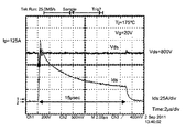
- FIG. 10 is an explanatory diagram showing a load short-circuit withstand test result of Example 1.
- the power supply voltage Vds 800 V and the measurement temperature was 175 ° C.
- FIG. 10 the schematic of the measurement waveform in a load short circuit tolerance test is shown. As is clear from the results shown in FIG. 10, sufficient characteristics were exhibited that no breakdown occurs even when 250 A, whose maximum current is five times the element rating, is conducted, and further no breakdown occurs even at 15 ⁇ sec.
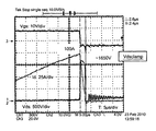
- FIG. 11 is an explanatory diagram showing the turn-off breakdown resistance evaluation results of the SiC-MOSFET of Example 1.
- the source-drain voltage was clamped to 1650 V (Vdsclamp in FIG. 11), and 100 A (rated current) was not destroyed. 4 times) was confirmed to be off at 150 ° C. From this, it can be said that the SiC-MOSFET of Example 1 according to the present invention is a device that achieves a low on-resistance and has extremely large load short-circuit withstand capability and turn-off capability.
- the N-type SiC semiconductor substrate 1 was similarly formed on a surface where the crystallographic plane index was inclined at 0 °, 2 °, 8 °, and 10 ° with respect to (000-1), When the device was evaluated, the characteristics were almost unchanged and good.
- FIG. 13 is an explanatory diagram showing a turn-off switching waveform of the SiC-MOSFET of Example 1, where (a) shows a measurement result at room temperature and (b) shows a measurement result at 200 ° C.
- FIGS. 14A and 14B are explanatory diagrams showing turn-on switching waveforms of the SiC-MOSFET of Example 1.
- FIG. 14A shows a measurement result at room temperature
- FIG. 14B shows a measurement result at 200.degree.
- Example 2 a second embodiment according to the present invention will be described.
- the N-type SiC semiconductor substrate 1 has an N-type containing about 1.8 ⁇ 10 16 cm ⁇ 3 on the surface where the crystallographic plane index is inclined about 4 degrees with respect to (0001).
- the SiC layer 2 was epitaxially grown by about 10 ⁇ m.
- the process and cell structure for forming other than the N-type SiC layer 2 are the same as those in Example 1 described above, and thus the description thereof is omitted.
- the on-resistance of the SiC-MOSFET of the second embodiment increases by about 55% with respect to the on-resistance of the SiC-MOSFET of the first embodiment. It can be seen that the on-resistance characteristics are sufficiently low. It should be noted that the N-type SiC semiconductor substrate 1 was similarly formed on a surface where the crystallographic plane index was inclined at 0 °, 2 °, 8 °, and 10 ° with respect to (0001), and the device evaluation was also performed on the created device. As a result, it was found that there was almost no change in characteristics.
- Example 3 a third embodiment according to the present invention will be described.
- a description will be given by taking as an example a 1200 V / 25 A MOSFET manufactured by the same manufacturing process as in the first embodiment.
- Example 3 about 1.8 ⁇ 10 16 cm ⁇ 3 of nitrogen is included on the surface where the crystallographic plane index of the N-type SiC semiconductor substrate 1 is inclined about 4 degrees with respect to (000-1).
- the N-type SiC layer 2 was epitaxially grown by about 10 ⁇ m.
- FIG. 12 is a plan view showing the arrangement of the P + layer 3 and the cell in the SiC-MOSFET of the third embodiment.
- the N-type SiC layer 2 was designed with a stripe cell pattern.
- the P + layer 3 has an arrangement in which the P + layer 3 is coupled in a structure as shown in FIG.
- the P + layer 3 is bonded under the N-turnback layer 6 and the P base layer 4.
- the steps for forming other than the N-type SiC layer 2 are the same as those in Examples 1 and 2 described above, and thus the description thereof is omitted.
- the on-resistance of the SiC-MOSFET of the third embodiment increases by about 10% with respect to the on-resistance of the SiC-MOSFET of the first embodiment. It can be seen that the on-resistance characteristic and the high breakdown voltage characteristic are sufficiently low.
- Example 4 Next, a fourth embodiment according to the present invention will be described.
- an N-type SiC semiconductor substrate is prepared as the semiconductor substrate 1.
- a low resistance N-type SiC semiconductor substrate 1 containing about 2 ⁇ 10 19 cm ⁇ 3 of nitrogen as an impurity is used as a semiconductor substrate.
- nitrogen is 1.8 ⁇ 10 16 cm ⁇ 3.
- the N-type SiC layer 2 containing about 10 ⁇ m is epitaxially grown.
- a P + layer (second semiconductor layer) 3 is formed on the N-type SiC layer 2 epitaxially grown on the N-type SiC semiconductor substrate 1 by an epitaxial method.
- the P + layer 3 has a width of 13 ⁇ m and a thickness of 0.5 ⁇ m.
- aluminum is used as impurity ions. The dose is set so that the impurity concentration in forming the P + layer 3 is 1.0 ⁇ 10 18 cm ⁇ 3 .
- the N-turnback layer 6 when the N-turnback layer 6 is formed, a part of the P + layer 3 is bonded to each other as in the first embodiment (see FIG. 6).
- a hexagonal cell pattern is used, but there is no problem with a quadrangular cell.
- the distance between the P + layers 3 that are not bonded is, for example, 2 ⁇ m.
- the P base layer 4 is formed to have a thickness of 0.5 ⁇ m by an epitaxial growth method.
- aluminum is used as an impurity, and the impurity concentration is set to 2.0 ⁇ 10 16 cm ⁇ 3 .
- nitrogen ions are selectively implanted into the P base layer 4 as the N repelling layer 6 to selectively form the N + source layer 7 and the P + contact layer 8 in the P base layer 4.
- concentration, thickness, and width of the N-turnback layer 6 are the same as those in the first embodiment.
- a gate insulating film 9 having a thickness of 100 nm is formed by thermal oxidation and annealed in the vicinity of 1000 ° C. in a hydrogen atmosphere. Then, a polycrystalline Si layer doped with phosphorus is formed as a gate electrode 10 and patterned. The gate electrode 10 is provided on at least a part of the surface exposed portion of the P base layer 4 sandwiched between the N + source layer 7 and the N return layer 6 via the gate insulating film 9.
- phosphorous glass is formed to a thickness of 1.0 ⁇ m and patterned, and then heat treatment is performed to form the interlayer insulating film 14. Then, after the interlayer insulating film 14 is formed, aluminum containing 1% Si is formed on the surface with a thickness of 5 ⁇ m by sputtering, and the source electrode 11 is formed.
- a nickel film is formed on the back side of the N-type SiC semiconductor substrate 1, heat-treated at 970 ° C., Ti / Ni / Au is formed, and the drain electrode 12 is formed. Thereafter, the SiC-MOSFET of Example 4 is completed by adding a protective film to the surface.
- the on-resistance (RonA) of the SiC-MOSFET of Example 4 manufactured in this way is a sufficiently low value of 2.85 m ⁇ cm 2. ing. Further, the SiC-MOSFET of Example 4 has an initial device breakdown voltage of 1455 V, and exhibits sufficiently good characteristics as a 1200 V device.
- the N-type semiconductor substrate 1 was similarly formed on the surface where the crystallographic plane index was inclined by 0 °, 2 °, 8 °, and 10 ° with respect to (000-1), and the produced element was also the same.
- the characteristics were almost unchanged and good.
- the chip size is 3 mm square, the active area is 5.27 mm 2 , and the rated current is 25A.
- Example 5 a fifth embodiment according to the present invention will be described.
- the N-type SiC semiconductor substrate 1 has an N-type containing about 1.8 ⁇ 10 16 cm ⁇ 3 on the surface where the crystallographic plane index is inclined about 4 degrees with respect to (0001).
- the SiC layer 2 was epitaxially grown by about 10 ⁇ m. The other steps are the same as those in Example 4.
- the on-resistance of the SiC-MOSFET of the fifth embodiment increases by about 50% with respect to the on-resistance of the SiC-MOSFET of the fourth embodiment. It can be seen that the on-resistance characteristics are sufficiently low. It should be noted that an element evaluation was also made on an element manufactured by similarly forming a film on a surface in which the crystallographic plane index of the N-type SiC semiconductor substrate 1 was inclined at 0 °, 2 °, 8 °, or 10 ° with respect to (0001). As a result, it was found that there was almost no change in characteristics.
- the present invention is not limited to being applied to a MOSFET.
- the present invention can also be applied to an IGBT using a semiconductor substrate having a conductivity type different from that of a MOSFET. That is, in each embodiment, the first conductivity type is N-type and the second conductivity type is P-type. However, in the present invention, the first conductivity type is P-type and the second conductivity type is N-type. It holds.
- the MOSFET of the present invention includes the N-type SiC semiconductor substrate 1 as the first conductivity-type semiconductor substrate and the first conductivity-type N-type SiC semiconductor substrate formed on the N-type SiC semiconductor substrate 1.
- N-type SiC layer 2 as a first semiconductor layer having an impurity concentration lower than 1 and a second conductivity type selectively formed on the surface of N-type SiC layer 2 and having an impurity concentration higher than that of N-type SiC layer 2
- An N + source layer 7 as a first conductivity type source region selectively formed on the surface layer, and a first conductivity type formed so as to penetrate the P base layer 4 from the surface to reach the N type SiC layer 2 Sandwiched between the N reversal layer 6, the N + source layer 7 and the N reversal layer 6 Common to the surface of the
- the SiC-MOSFET of the embodiment of the present invention even if the on-resistance is sufficiently lowered by greatly increasing the impurity concentration in the regions of the N-type SiC layer 2 and the N-turnback layer 6 which are low-concentration N-type semiconductor layers. Or, even when the distance between the P + layer 3 and the P base layer 4 is increased to reduce the on-resistance sufficiently, or when a high voltage is applied between the source and the drain (the source is 0 V and the drain is + voltage). And a large electric field is not applied to the gate insulating film 9 on the region 6 of the N strike back layer. As a result, a sufficient element breakdown voltage can be maintained. This is because the depletion layer tends to spread laterally along the P + layer 3.
- the impurity concentration in the region of N-type SiC layer 2 and N Uchikaeshi layer 6 be set higher than the conventional MOSFET, a depletion layer that spreads easily design, between the P + layer 3 and the P base layer 4
- the on-resistance can be reduced while maintaining a sufficient element breakdown voltage by increasing the distance between them.
- SiC-MOSFET or IGBT structure of the embodiment according to the present invention
- a high voltage is applied while utilizing its low on-resistance characteristics. Even at this time, it is possible to improve the reliability by preventing the oxide film forming the gate electrode 10 from being broken, and to exhibit the low on-resistance of SiC.
- the P base layer 4 of the embodiment according to the present invention is formed by the epitaxial growth method, it can be made flat so that there is almost no surface roughness, so that the mobility of the MOSFET portion on the surface becomes extremely large. As a result, the on-resistance can be further reduced.
- the crystallographic plane index of the N-type SiC semiconductor substrate 1 is a plane parallel to (000-1) or within 10 degrees, or the crystallography of the N-type semiconductor substrate 1
- the interface state density between the gate insulating film 9 and the semiconductor interface can be reduced, so that the mobility of the MOSFET portion can be further improved. it can.
- the on-resistance can be made extremely small.
- the P + which is the second semiconductor layer can be changed only by changing the mask for forming the P + layer 3 by ion implantation into the surface of the N-repelling layer 6.
- a part of the layer 3 can be bonded to each other, thereby causing a high breakdown resistance with a low on-resistance while maintaining a sufficient device breakdown voltage characteristic regardless of the crystal plane orientation of the substrate without incurring a cost increase.
- MOSFETs and IGBTs capable of high-speed switching characteristics.
- each embodiment is similarly achieved even if the conductivity type (N type, P type) of the semiconductor layer or semiconductor region is inverted.
- the semiconductor substrate is described as an N-type MOSFET, but the same effect can be achieved in an IGBT.
- a P-type collector layer may be formed on the back surface of the substrate by a technique such as epitaxial growth or ion implantation.
- the MOSFET of the present invention is applied to an IGBT, the conductivity type of the N-type SiC semiconductor substrate 1 as a semiconductor substrate is changed from N-type to P-type, or a P-type collector layer is formed on the back surface of the N-type substrate. That's fine.
- the SiC-MOSFET (or IGBT structure) of the embodiment according to the present invention it is possible to provide a vertical MOSFET, an IGBT structure and a simple manufacturing method thereof.
- the vertical high-voltage semiconductor device and the method for manufacturing the vertical high-voltage semiconductor device according to the present invention include power used for power conversion devices such as an inverter for motor control and an uninterruptible power supply (UPS). Useful for semiconductor devices.
- power conversion devices such as an inverter for motor control and an uninterruptible power supply (UPS).
- UPS uninterruptible power supply
Landscapes
- Electrodes Of Semiconductors (AREA)
- Insulated Gate Type Field-Effect Transistor (AREA)
- Chemical & Material Sciences (AREA)
- Composite Materials (AREA)
Abstract
Description
以下、本発明の実施例1について、図5を参照して説明する。図5は、実施例1のSiC-MOSFETの各製造工程における断面図であり、図5(a)はP+層を結合していない部分、図5(b)はP+層(IGBTの場合は、P+基板)を結合している部分の断面図を示している。本実施例1においては、縦型プレーナーゲートMOSFETとして、半導体材料として炭化ケイ素(SiC)を用い、素子耐圧1200VのMOSFETを例に挙げて説明する。
つぎに、この発明にかかる実施例2について説明する。実施例2においては、実施例1と同様の製造工程により作製した、1200V・25AのMOSFETを例にして説明する。実施例2においては、N型SiC半導体基板1の結晶学的面指数が(0001)に対して4度程度傾いた面の上に、窒素を1.8×1016cm-3程度含むN型SiC層2を10μm程度エピタキシャル成長させた。実施例2において、N型SiC層2以外を形成する工程やセル構造については、上述した実施例1とすべて同一であるため、説明を省略する。
つぎに、この発明にかかる実施例3について説明する。実施例3においては、実施例1と同様の製造工程により作製した、1200V・25AのMOSFETを例にして説明する。実施例3においては、N型SiC半導体基板1の結晶学的面指数が(000-1)に対して4度程度傾いた面の上に、窒素を1.8×1016cm-3程度含むN型SiC層2を、10μm程度エピタキシャル成長させた。
つぎに、この発明にかかる実施例4について説明する。実施例4においては、まず、半導体基板1としてN型SiC半導体基板を用意する。実施例4では、不純物として窒素を2×1019cm-3程度含む低抵抗N型SiC半導体基板1を半導体基板とする。実施例4においては、N型SiC半導体基板1の結晶学的面指数が(000-1)に対して4度程度傾いた面の上に、たとえば、窒素を1.8×1016cm-3程度含むN型SiC層2を、10μm程度エピタキシャル成長させる。
つぎに、この発明にかかる実施例5について説明する。実施例5においては、実施例4と同様の製造工程により作製した、1200V・25AのMOSFETを例にして説明する。実施例5においては、N型SiC半導体基板1の結晶学的面指数が(0001)に対して4度程度傾いた面の上に、窒素を1.8×1016cm-3程度含むN型SiC層2を10μm程度エピタキシャル成長させた。その他の工程は、実施例4とすべて同一とする。
2 第1の半導体層
3 P+層
4 Pベース層
6 N打ち返し層
7 N+ソース層
8 P+コンタクト層
9 ゲート絶縁膜
10 ゲート電極
11 ソース電極
12 ドレイン電極
13 連結部
Claims (6)
- 第1導電型の半導体基板(1)と、
前記半導体基板(1)上に形成された第1導電型で前記半導体基板(1)よりも不純物濃度が低い第1の半導体層(2)と、
前記第1の半導体層(2)の表面に選択的に形成された第2導電型で第1の半導体層(2)よりも不純物濃度が高い第2の半導体層(3)と、
前記第1の半導体層(2)および前記第2の半導体層(3)の上に設けられた第2導電型のベース層(4)と、
前記ベース層(4)の表面層に選択的に形成された第1導電型ソース領域(7)と、
表面から前記ベース層(4)を貫通して前記第1の半導体層(2)に達するように形成された第1導電型のN打ち返し層(6)と、
前記ソース領域(7)と前記N打ち返し層(6)とに挟まれた前記ベース層(4)の表面露出部上の少なくとも一部にゲート絶縁膜(9)を介して設けられたゲート電極層(10)と、
前記ソース領域(7)と前記ベース層(4)との表面に共通に接触するソース電極(11)と、
前記半導体基板(1)の裏面に設けられたドレイン電極(12)と、
を有する縦型高耐圧半導体装置であって、
前記第2の半導体層(3)の一部は、前記N打ち返し層(6)の下の領域で互いに結合されていることを特徴とする縦型高耐圧半導体装置。 - 前記第2の半導体層(3)の一部が前記N打ち返し層(6)の下の領域で結合されている部分は、前記ベース層(4)と前記N打ち返し層(6)で形成されるPN接合から離隔していることを特徴とする請求項1に記載の縦型高耐圧半導体装置。
- 前記半導体基板(1)の半導体材料が炭化ケイ素であることを特徴とする請求項1または2に記載の縦型高耐圧半導体装置。
- 前記半導体基板(1)の結晶学的面指数が(000-1)に対して平行な面もしくは10度以内に傾いた面であることを特徴とする請求項3に記載の縦型高耐圧半導体装置。
- 前記半導体基板(1)の結晶学的面指数が(0001)に対して平行な面もしくは10度以内に傾いた面であることを特徴とする請求項4に記載の縦型高耐圧半導体装置。
- 第1導電型の半導体基板(1)上に第1導電型で前記半導体基板(1)よりも不純物濃度が低い第1の半導体層(2)を形成する工程と、
前記第1の半導体層(2)の表面に、第2導電型で第1の半導体層(2)よりも不純物濃度が高い第2の半導体層(3)をイオン注入法により選択的に形成する工程と、
前記第1の半導体層(2)および前記第2の半導体層(3)の上に、エピタキシャル成長法により第2導電型のベース層(4)を形成する工程と、
前記ベース層(4)の表面層に選択的に形成された第1導電型ソース領域(7)と、表面から前記ベース層(4)を貫通して前記第1の半導体層(2)に達する第1導電型のN打ち返し層(6)と、をイオン注入法により形成する工程と、
を含み、
前記第2の半導体層(3)を形成する工程は、前記第2の半導体層(3)の一部が、前記N打ち返し層(6)の下の領域で互いに結合されるように形成することを特徴とする縦型高耐圧半導体装置の製造方法。
Priority Applications (5)
| Application Number | Priority Date | Filing Date | Title |
|---|---|---|---|
| DE112013001796.2T DE112013001796B4 (de) | 2012-03-30 | 2013-03-29 | Vertikale Hochspannungshalbleitervorrichtung und Herstellungsverfahren einer vertikalen Hochspannungshalbleitervorrichtung |
| CN201380018019.2A CN104303311B (zh) | 2012-03-30 | 2013-03-29 | 纵型高耐压半导体装置及纵型高耐压半导体装置的制造方法 |
| JP2014508244A JP5995252B2 (ja) | 2012-03-30 | 2013-03-29 | 縦型高耐圧半導体装置および縦型高耐圧半導体装置の製造方法 |
| US14/388,745 US9722018B2 (en) | 2012-03-30 | 2013-03-29 | Vertical high voltage semiconductor apparatus and fabrication method of vertical high voltage semiconductor apparatus |
| US15/423,739 US10211330B2 (en) | 2012-03-30 | 2017-02-03 | Vertical high voltage semiconductor apparatus and fabrication method of vertical high voltage semiconductor apparatus |
Applications Claiming Priority (2)
| Application Number | Priority Date | Filing Date | Title |
|---|---|---|---|
| JP2012081580 | 2012-03-30 | ||
| JP2012-081580 | 2012-03-30 |
Related Child Applications (2)
| Application Number | Title | Priority Date | Filing Date |
|---|---|---|---|
| US14/388,745 A-371-Of-International US9722018B2 (en) | 2012-03-30 | 2013-03-29 | Vertical high voltage semiconductor apparatus and fabrication method of vertical high voltage semiconductor apparatus |
| US15/423,739 Division US10211330B2 (en) | 2012-03-30 | 2017-02-03 | Vertical high voltage semiconductor apparatus and fabrication method of vertical high voltage semiconductor apparatus |
Publications (1)
| Publication Number | Publication Date |
|---|---|
| WO2013147276A1 true WO2013147276A1 (ja) | 2013-10-03 |
Family
ID=49260514
Family Applications (1)
| Application Number | Title | Priority Date | Filing Date |
|---|---|---|---|
| PCT/JP2013/059777 Ceased WO2013147276A1 (ja) | 2012-03-30 | 2013-03-29 | 縦型高耐圧半導体装置および縦型高耐圧半導体装置の製造方法 |
Country Status (5)
| Country | Link |
|---|---|
| US (2) | US9722018B2 (ja) |
| JP (1) | JP5995252B2 (ja) |
| CN (1) | CN104303311B (ja) |
| DE (1) | DE112013001796B4 (ja) |
| WO (1) | WO2013147276A1 (ja) |
Cited By (2)
| Publication number | Priority date | Publication date | Assignee | Title |
|---|---|---|---|---|
| CN103594504A (zh) * | 2013-11-19 | 2014-02-19 | 西安永电电气有限责任公司 | 具有半超结结构的igbt |
| JP2020021744A (ja) * | 2017-03-07 | 2020-02-06 | 株式会社島津製作所 | イオントラップ装置 |
Families Citing this family (8)
| Publication number | Priority date | Publication date | Assignee | Title |
|---|---|---|---|---|
| US9881997B2 (en) * | 2015-04-02 | 2018-01-30 | Fuji Electric Co., Ltd. | Semiconductor device and manufacturing method of semiconductor device |
| CN107408577B (zh) * | 2015-09-17 | 2020-09-08 | 富士电机株式会社 | 半导体装置及半导体装置的制造方法 |
| JP7099158B2 (ja) * | 2018-08-09 | 2022-07-12 | 富士電機株式会社 | 模擬素子及び抵抗素子の不良検査方法 |
| JP7171527B2 (ja) * | 2019-09-13 | 2022-11-15 | 株式会社 日立パワーデバイス | 半導体装置および電力変換装置 |
| JP7292175B2 (ja) * | 2019-10-16 | 2023-06-16 | 株式会社東芝 | 半導体装置 |
| WO2021210547A1 (ja) * | 2020-04-14 | 2021-10-21 | 国立研究開発法人産業技術総合研究所 | 半導体装置 |
| US11784247B2 (en) * | 2020-06-10 | 2023-10-10 | Electronics And Telecommunications Research Institute | MOS(metal oxide silicon) controlled thyristor device |
| US20240421029A1 (en) * | 2023-06-16 | 2024-12-19 | Wolfspeed, Inc. | Semiconductor Package |
Citations (3)
| Publication number | Priority date | Publication date | Assignee | Title |
|---|---|---|---|---|
| WO2004036655A1 (ja) * | 2002-10-18 | 2004-04-29 | National Institute Of Advanced Industrial Science And Technology | 炭化ケイ素半導体装置及びその製造方法 |
| JP2009099714A (ja) * | 2007-10-16 | 2009-05-07 | Oki Semiconductor Co Ltd | 半導体装置とその製造方法 |
| JP2011258635A (ja) * | 2010-06-07 | 2011-12-22 | Mitsubishi Electric Corp | 半導体装置 |
Family Cites Families (4)
| Publication number | Priority date | Publication date | Assignee | Title |
|---|---|---|---|---|
| US7221010B2 (en) | 2002-12-20 | 2007-05-22 | Cree, Inc. | Vertical JFET limited silicon carbide power metal-oxide semiconductor field effect transistors |
| US7118970B2 (en) * | 2004-06-22 | 2006-10-10 | Cree, Inc. | Methods of fabricating silicon carbide devices with hybrid well regions |
| JP4900662B2 (ja) * | 2006-03-02 | 2012-03-21 | 独立行政法人産業技術総合研究所 | ショットキーダイオードを内蔵した炭化ケイ素mos電界効果トランジスタおよびその製造方法 |
| EP2091083A3 (en) | 2008-02-13 | 2009-10-14 | Denso Corporation | Silicon carbide semiconductor device including a deep layer |
-
2013
- 2013-03-29 CN CN201380018019.2A patent/CN104303311B/zh active Active
- 2013-03-29 JP JP2014508244A patent/JP5995252B2/ja active Active
- 2013-03-29 DE DE112013001796.2T patent/DE112013001796B4/de active Active
- 2013-03-29 US US14/388,745 patent/US9722018B2/en active Active
- 2013-03-29 WO PCT/JP2013/059777 patent/WO2013147276A1/ja not_active Ceased
-
2017
- 2017-02-03 US US15/423,739 patent/US10211330B2/en active Active
Patent Citations (3)
| Publication number | Priority date | Publication date | Assignee | Title |
|---|---|---|---|---|
| WO2004036655A1 (ja) * | 2002-10-18 | 2004-04-29 | National Institute Of Advanced Industrial Science And Technology | 炭化ケイ素半導体装置及びその製造方法 |
| JP2009099714A (ja) * | 2007-10-16 | 2009-05-07 | Oki Semiconductor Co Ltd | 半導体装置とその製造方法 |
| JP2011258635A (ja) * | 2010-06-07 | 2011-12-22 | Mitsubishi Electric Corp | 半導体装置 |
Cited By (2)
| Publication number | Priority date | Publication date | Assignee | Title |
|---|---|---|---|---|
| CN103594504A (zh) * | 2013-11-19 | 2014-02-19 | 西安永电电气有限责任公司 | 具有半超结结构的igbt |
| JP2020021744A (ja) * | 2017-03-07 | 2020-02-06 | 株式会社島津製作所 | イオントラップ装置 |
Also Published As
| Publication number | Publication date |
|---|---|
| JP5995252B2 (ja) | 2016-09-21 |
| US20170213886A1 (en) | 2017-07-27 |
| US10211330B2 (en) | 2019-02-19 |
| DE112013001796T5 (de) | 2014-12-18 |
| JPWO2013147276A1 (ja) | 2015-12-14 |
| CN104303311A (zh) | 2015-01-21 |
| US20150076519A1 (en) | 2015-03-19 |
| CN104303311B (zh) | 2017-10-13 |
| DE112013001796B4 (de) | 2018-03-29 |
| US9722018B2 (en) | 2017-08-01 |
Similar Documents
| Publication | Publication Date | Title |
|---|---|---|
| JP5995252B2 (ja) | 縦型高耐圧半導体装置および縦型高耐圧半導体装置の製造方法 | |
| JP6074787B2 (ja) | 炭化珪素半導体装置およびその製造方法 | |
| US10263105B2 (en) | High voltage semiconductor device | |
| US9627486B2 (en) | Semiconductor device | |
| US9362392B2 (en) | Vertical high-voltage semiconductor device and fabrication method thereof | |
| US8564028B2 (en) | Low on-resistance wide band gap semiconductor device and method for producing the same | |
| JP5613995B2 (ja) | 炭化珪素半導体装置およびその製造方法 | |
| JP2010206002A (ja) | pチャネル型炭化珪素MOSFET | |
| JP2015056644A (ja) | 炭化珪素半導体装置および炭化珪素半導体装置の製造方法 | |
| CN111430449A (zh) | 一种mosfet器件及其制备工艺 | |
| CN105845718B (zh) | 一种4H-SiC沟槽型绝缘栅双极型晶体管 | |
| CN104321875B (zh) | 高耐压半导体装置 | |
| JP2010258385A (ja) | 炭化珪素半導体装置およびその製造方法 | |
| JP2018064047A (ja) | 半導体装置および半導体装置の製造方法 | |
| JP7333509B2 (ja) | 炭化珪素半導体装置 |
Legal Events
| Date | Code | Title | Description |
|---|---|---|---|
| 121 | Ep: the epo has been informed by wipo that ep was designated in this application |
Ref document number: 13768322 Country of ref document: EP Kind code of ref document: A1 |
|
| WWE | Wipo information: entry into national phase |
Ref document number: 14388745 Country of ref document: US |
|
| ENP | Entry into the national phase |
Ref document number: 2014508244 Country of ref document: JP Kind code of ref document: A |
|
| WWE | Wipo information: entry into national phase |
Ref document number: 1120130017962 Country of ref document: DE Ref document number: 112013001796 Country of ref document: DE |
|
| 122 | Ep: pct application non-entry in european phase |
Ref document number: 13768322 Country of ref document: EP Kind code of ref document: A1 |