WO2013147207A1 - 磁界強度の測定方法、フラックスゲート型磁気素子および磁気センサ - Google Patents
磁界強度の測定方法、フラックスゲート型磁気素子および磁気センサ Download PDFInfo
- Publication number
- WO2013147207A1 WO2013147207A1 PCT/JP2013/059642 JP2013059642W WO2013147207A1 WO 2013147207 A1 WO2013147207 A1 WO 2013147207A1 JP 2013059642 W JP2013059642 W JP 2013059642W WO 2013147207 A1 WO2013147207 A1 WO 2013147207A1
- Authority
- WO
- WIPO (PCT)
- Prior art keywords
- magnetic
- magnetic field
- coil
- feedback
- magnetic core
- Prior art date
- Legal status (The legal status is an assumption and is not a legal conclusion. Google has not performed a legal analysis and makes no representation as to the accuracy of the status listed.)
- Ceased
Links
Images




Classifications
-
- G—PHYSICS
- G01—MEASURING; TESTING
- G01R—MEASURING ELECTRIC VARIABLES; MEASURING MAGNETIC VARIABLES
- G01R33/00—Arrangements or instruments for measuring magnetic variables
- G01R33/02—Measuring direction or magnitude of magnetic fields or magnetic flux
- G01R33/04—Measuring direction or magnitude of magnetic fields or magnetic flux using the flux-gate principle
- G01R33/05—Measuring direction or magnitude of magnetic fields or magnetic flux using the flux-gate principle in thin-film element
-
- G—PHYSICS
- G01—MEASURING; TESTING
- G01R—MEASURING ELECTRIC VARIABLES; MEASURING MAGNETIC VARIABLES
- G01R33/00—Arrangements or instruments for measuring magnetic variables
- G01R33/02—Measuring direction or magnitude of magnetic fields or magnetic flux
- G01R33/04—Measuring direction or magnitude of magnetic fields or magnetic flux using the flux-gate principle
Definitions
- the present invention relates to a method for measuring magnetic field strength, a fluxgate type magnetic element, and a magnetic sensor.
- This application claims priority on March 30, 2012 based on Japanese Patent Application No. 2012-083253 for which it applied to Japan, and uses the content here.
- a flux gate type magnetic element is known as a magnetic element for measuring the strength of a magnetic field.
- the flux gate type magnetic element has a feature of being small and highly sensitive, and is used as an electronic compass for measuring geomagnetism or a current sensor for measuring a magnetic field strength generated by an electric current and converting it into a current value.
- Patent Document 1 As an example of a conventional flux gate type magnetic element, there is a flux gate type magnetic element disclosed in Patent Document 1.
- an excitation coil and a detection coil are wound around a thin-film magnetic core.
- the flux gate type magnetic element of Patent Document 1 outputs magnetic field strength based on the following detection principle.
- a triangular wave excitation current that fluctuates at a constant period is applied to an excitation coil wound around a magnetic core material.
- the magnetic core repeats magnetization saturation and magnetization reversal along the BH curve by the triangular wave excitation magnetic field generated by the triangular wave excitation current. When this magnetization direction is reversed, a pulsed voltage signal is generated in the detection coil.
- an external magnetic field that is a magnetic field to be measured is applied. Since the external magnetic field is added to the excitation magnetic field generated by the triangular wave excitation current, the timing at which the pulse voltage signal is generated is shifted by the magnitude of the external magnetic field. An output corresponding to the magnitude of the external magnetic field can be obtained by taking out the time change generated by the pulse voltage signal by the detection circuit.
- the conventional fluxgate type magnetic element has the following problems.
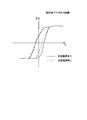
- the magnetic core of the fluxgate type magnetic element has a magnetic saturation characteristic of a BH curve as shown by a broken line in FIG.
- the BH curve has a region where the relationship between the magnetic field H applied to the magnetic core and the magnetic flux density B of the magnetic core changes linearly with the origin of the graph as the center of symmetry.
- the flux gate type magnetic element measures the magnetic field strength by using the magnetic saturation characteristics of this linear region.
- a magnetic core made of a general magnetic material when an external magnetic field is applied, the magnetic saturation characteristics of the magnetic core change, and as shown by the solid line in FIG. Linearity also changes. That is, when an external magnetic field is applied, the relationship between the magnetic field H and the magnetic flux B is disturbed.
- the degree of the disturbance varies depending on the range of the applied external magnetic field, and the greater the applied external magnetic field, the greater the degree of deterioration of the linearity of the BH curve.
- the timing at which the pulsed voltage signal generated in the detection coil described above changes depending on the range of the external magnetic field, and particularly when a large magnetic field is applied the magnetic strength can be measured with high accuracy. It was difficult.
- the present invention provides a magnetic field strength measuring method, a flux gate type magnetic element, and a magnetic sensor capable of measuring magnetic field strength with high accuracy even when a large external magnetic field is applied to the flux gate type magnetic element. .
- the fluxgate magnetic element according to the first aspect of the present invention is a fluxgate magnetic element formed on a nonmagnetic substrate, and includes a magnetic core, an excitation coil wound around the magnetic core, And a detection coil wound around the magnetic core and a feedback coil wound around the magnetic core.
- the fluxgate magnetic element since the feedback coil is provided, it is possible to apply a feedback magnetic field that cancels the measured magnetic field in the magnetic core. Therefore, it is possible to reduce the effective magnetic field strength in the magnetic core, and the measurement of the magnetic field strength using the magnetic saturation characteristic in a state where the linearity of the BH curve indicating the magnetic saturation characteristic of the magnetic core is good. Is done. Therefore, it is possible to provide a fluxgate magnetic element capable of measuring the magnetic field strength with high accuracy.
- a magnetic sensor includes a magnetic core, and a first solenoid coil and a second solenoid coil wound around the magnetic core.
- One of the two solenoid coils is an excitation coil and the other is a detection coil, and cancels out the magnetic field to be measured in the magnetic core having a feedback coil wound around the magnetic core.
- a control integrated circuit for supplying a feedback current to the feedback coil so as to generate a feedback magnetic field and outputting the intensity of the magnetic field to be measured based on the value of the feedback current.
- the magnetic sensor of the second aspect of the present invention since the feedback magnetic field is applied from the feedback coil so as to cancel the measured magnetic field in the magnetic core, even if a large measured magnetic field is applied, the magnetic core The effective magnetic field strength at can be reduced. Therefore, in the BH curve indicating the magnetic saturation characteristics of the magnetic core, the magnetic field strength is measured using the magnetic saturation characteristics with a good linearity, and the magnetic field strength can be measured with high accuracy. As a result, it is possible to obtain an output that maintains linearity (linearity) as a magnetic element without restricting the range of the magnetic field intensity to be measured regardless of the magnetic characteristics of the magnetic core.
- the magnetic field strength measurement method uses a fluxgate magnetic element including a magnetic core, and an excitation coil, a detection coil, and a feedback coil wound around the magnetic core.
- the feedback coil generates a feedback magnetic field that cancels the magnetic field to be measured in the magnetic core
- the fluxgate magnetic element is based on a value of a current supplied to the feedback coil. Outputs the strength of the measured magnetic field.
- the feedback magnetic field is applied from the feedback coil so as to cancel the magnetic field to be measured in the magnetic core, so even if a large magnetic field to be measured is applied, Effective magnetic field strength in the magnetic core can be reduced. Therefore, the linearity of the BH curve indicating the magnetic saturation characteristics of the magnetic core does not change, and the magnetic field strength is measured using the magnetic saturation characteristics with good linearity, and the magnetic field strength is measured with high accuracy. Can do.
- the magnetic field strength measurement method according to the fourth aspect of the present invention is the magnetic field strength measurement method according to the third aspect, wherein the feedback magnetic field strength may be substantially the same as the magnetic field strength of the magnetic field to be measured.
- the magnetic field effectively applied to the magnetic core is almost zero, and the most linear in the BH curve.
- the magnetic field strength is measured using the magnetic saturation characteristics in a good state, and the magnetic field strength can be measured with higher accuracy.
- the magnetic field strength measurement method according to the fifth aspect of the present invention is the magnetic field strength measurement method according to the third aspect or the fourth aspect, in which the current value of the current supplied to the feedback coil is the output from the detection coil. It may be determined based on.
- the value of the current supplied to the feedback coil is determined based on the output from the detection coil. Regardless of the magnetic characteristics of the core, it is possible to obtain an output that maintains linearity (linearity) as a magnetic element.
- the fluxgate magnetic element since the feedback coil is provided, it is possible to apply a feedback magnetic field that cancels the measured magnetic field in the magnetic core. Therefore, it is possible to reduce the effective magnetic field strength in the magnetic core, and the measurement of the magnetic field strength using the magnetic saturation characteristic in a state where the linearity of the BH curve indicating the magnetic saturation characteristic of the magnetic core is good. Is done. Therefore, it is possible to provide a fluxgate magnetic element capable of measuring the magnetic field strength with high accuracy.
- FIG. 1 is a top schematic view schematically showing a fluxgate magnetic element of a magnetic sensor according to a first embodiment of the present invention.
- FIG. 6 is a cross-sectional view taken along line a-a ′ in FIG. 5.
- FIG. 6 is a cross-sectional view taken along line b-b ′ in FIG. 5 and is a front cross-sectional view showing a manufacturing process of the fluxgate type magnetic element.
- FIG. 6 is a cross-sectional view taken along line b-b ′ in FIG. 5 and is a front cross-sectional view showing a manufacturing process of the fluxgate type magnetic element.
- FIG. 6 is a cross-sectional view taken along line b-b ′ in FIG. 5 and is a front cross-sectional view showing a manufacturing process of the fluxgate type magnetic element.
- FIG. 6 is a cross-sectional view taken along line b-b ′ in FIG. 5 and is a front cross-sectional view showing a manufacturing process of the fluxgate type magnetic element.
- FIG. 6 is a cross-sectional view taken along line b-b ′ in FIG. 5 and is a front cross-sectional view showing a manufacturing process of the fluxgate type magnetic element.
- FIG. 6 is a cross-section
- FIG. 6 is a cross-sectional view taken along line b-b ′ in FIG. 5 and is a front cross-sectional view showing a manufacturing process of the fluxgate type magnetic element. It is a front sectional view showing another example of the magnetic sensor according to the first embodiment of the present invention. It is a top view which shows roughly the other example of the fluxgate type
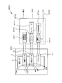
- FIG. 1 is a schematic diagram showing a magnetic sensor according to a first embodiment of the present invention.
- symbol MS10 has shown the magnetic sensor.
- the magnetic sensor MS10 includes a flux gate type magnetic element M12 and a control integrated circuit (signal processing circuit) MT10.
- the fluxgate magnetic element M12 includes an excitation coil 9, a detection coil 10, and a feed pack coil 21 wound around a magnetic core 1 made of a soft magnetic material.
- the control integrated circuit MT10 includes an exciting current generation circuit MT11, a sense amplifier MT12, a comparator MT13, a feedback control circuit (FB control circuit) MT14, a current amplifier MT15, and an output terminal MT16.
- the magnetic sensor MS10 is, for example, a current sensor for measuring a magnetic field to be measured created by a current flowing through a conductive path.
- the exciting coil 9 is connected to the exciting current generating circuit MT11. As will be described later, an exciting current signal having a continuous waveform is supplied to the exciting coil 9.
- the detection coil 10 is connected to the sense amplifier MT12. In the sense amplifier MT12, the output signal from the detection coil 10 is amplified.
- the sense amplifier MT12 is connected to the comparator MT13.
- the comparator MT13 is connected to the feedback control circuit MT14.
- the feedback control circuit MT14 is connected to the current amplifier MT15.
- the current amplifier MT15 is connected to the feed pack coil 21 and the output terminal MT16.
- a triangular wave exciting current generated by the exciting current generating circuit MT11 is supplied to the exciting coil 9, and an exciting magnetic field is generated in the magnetic core 1 accordingly.
- the direction of the magnetic field of the exciting magnetic field generated in the magnetic core 1 varies alternately between positive and negative.
- a pulsed induced voltage signal (detection signal) is generated at the timing when the direction of the magnetic field is switched.
- a pulse-like induced voltage signal (detection signal) generated in the detection coil 10 is input to the sense amplifier MT12 through a terminal connected to the detection coil 10.
- the sense amplifier MT12 amplifies this detection signal to the extent that the subsequent comparator MT13 can operate.
- the detection signal amplified by the sense amplifier MT12 is input to the comparator MT13.
- the comparator MT13 compares the voltage value of the amplified detection signal with a predetermined threshold voltage value, and outputs a high value signal or a low value signal according to the result. Thus, the comparator MT13 converts the detection signal into a PWM (Pulse Width Modulation) waveform.
- the ratio between the high value maintaining time and the low value maintaining time output by the comparator MT13 is called a duty ratio. If the duty ratio is 50:50, an external magnetic field (magnetic field to be measured) is not applied. If it deviates from 50:50, an external magnetic field (magnetic field to be measured) is being applied. A larger deviation from 50:50 indicates that a larger external magnetic field (magnetic field to be measured) is being applied.
- the feedback control circuit MT14 outputs a DC voltage signal having a value corresponding to the amount of deviation when the duty ratio between the high value maintenance time and the low value maintenance time output from the comparator MT13 is deviated from 50:50. To do.
- the current amplifier MT15 supplies the feedback coil 21 with a feed pack current for bringing the duty ratio close to 50:50 based on the DC voltage signal output from the feedback control circuit MT14. Thereby, the magnetization state in the magnetic core is effectively a state in which no external magnetic field is applied.
- FIG. 2 is a graph showing the operating principle of the fluxgate magnetic element.
- FIG. 2A is a graph showing the change over time of the triangular wave excitation current supplied to the excitation coil.
- FIG. 2B is a graph showing the time change of the magnetization state of the core.
- FIG. 2C is a graph showing a time change of the detection signal generated in the detection coil.
- FIG. 3 is a BH curve (hysteresis curve) showing a change with time of the magnetization state of the magnetic core of the fluxgate type magnetic element M12.
- FIG. 2A When a triangular wave excitation current as shown in FIG. 2A is supplied from the excitation current generation circuit MT11 to the excitation coil 9, an excitation magnetic field is generated in the magnetic core 1 by the excitation magnetic field Hexc created by the excitation coil 9.
- the horizontal axis represents time
- the vertical axis represents the current value. Since the magnetic core 1 has a magnetic saturation characteristic as shown in FIG. 3, the magnetization state in the magnetic core 1 changes with time as shown in FIG.
- FIG. 2B the horizontal axis represents time
- the vertical axis represents the magnetic flux density B in the magnetic core 1.
- the detection coil 10 is proportional to the cross-sectional area S of the magnetic core 1 and the number of turns N of the pickup coil 10 at the timing when the polarity of the magnetization state of the magnetic core 1 is reversed, that is, when the time change dB / dt is present.
- the induced voltage Vpu NS ⁇ dB / dt is generated.
- the induced voltage Vpu generated in the detection coil 10 is a pulsed induced voltage signal (detection signal) that changes with time as shown in FIG. In FIG. 2C, the horizontal axis represents time, and the vertical axis represents the voltage value.
- the time interval t1 in FIG. 2C is the external magnetic field (measured magnetic field) Hext, the deviation Hc of the magnetic field strength H between when the magnetic flux density B of the magnetic core 1 increases and when it decreases, and the exciting coil 9 (1) using the magnetic field Hexc, the period T of the triangular wave excitation current, and the delay time Td due to the inductance of the coil.
- This excitation efficiency ⁇ indicates the ratio between the magnetic flux density generated in the magnetic core 1 by passing a triangular wave excitation current through the exciting coil 9 and the magnetic flux density generated in the magnetic core 1 by an external magnetic field.
- the excitation efficiency ⁇ corresponds to the slope dB / dHext of the magnetic density B with respect to the external magnetic field Hext in the non-saturated region of the hysteresis curve of the magnetic core 1 and the triangular wave excitation current Iexc flowing through the excitation coil of the magnetic core 1 with the magnetic flux density B. It is determined by the ratio of the slope dB / dIexc and is expressed by the equation (4).
- the magnetic sensor MS10 supplies the exciting current having a triangular waveform continuously oscillating from the exciting current generating circuit MT11 of the control integrated circuit (signal processing circuit) MT10 to the exciting coil 9, and the magnetic core 1 generates a magnetic field in which the direction of the magnetic flux continuously vibrates and saturates.
- a pulsed induced voltage is generated in the detection coil 10 at the timing when the direction of the magnetic flux is reversed.
- the time interval T0 of the pulse-like induced voltage signal output from the detection coil 10 is set to the magnetic core 1 so that the difference between when the external magnetic field Hext is not applied and when it is applied is minimized.
- a feedback current is supplied to the wound feedback coil 21.
- the exciting current generating circuit MT11 supplies the exciting coil 9 with a triangular wave exciting current that varies with the period T. Along with this, an exciting magnetic field is generated in the magnetic core 1.
- FIG. 10A the exciting current generating circuit MT11 supplies the exciting coil 9 with a triangular wave exciting current that varies with the period T. Along with this, an exciting magnetic field is generated in the magnetic core 1.
- 10C shows a pulsed induced voltage signal generated in the detection coil 10 when the magnetization state of the magnetic core 1 is reversed.
- a positive sign induced voltage signal K + is generated.
- the negative induced voltage signal K ⁇ is generated.
- the induced voltage signals (K +, K ⁇ ) generated in the detection coil 10 are input to the control integrated circuit MT10 as the output of the fluxgate magnetic element M12.
- the induced voltage signal is amplified by the sense amplifier MT12 and then input to the comparator MT13.
- the comparator MT13 modulates the amplified induced voltage signal into a PWM (Pulse Width Modulation) waveform. That is, the voltage value of the amplified induced voltage signal is compared with a predetermined threshold voltage value. If the voltage value of the amplified induced voltage signal is larger, High is maintained, and the amplified induced voltage signal is If is smaller, a voltage signal maintaining Low is output.
- PWM Pulse Width Modulation
- T H T L
- T H T L
- T0 50: 50
- the signal modulated by the comparator MT13 is input to an LPF (low-pass filter) feedback control circuit 14.
- the timing at which the magnetization state (magnetization direction) in the magnetic core 1 is reversed is not synchronized with the fluctuation of the triangular wave current of the exciting coil 9.
- the timing at which the magnetization direction of the magnetic core is reversed from negative to positive approaches time t3 and t7 as a shift from time t2 and t6, respectively.
- the timing at which the positive-polarized induced voltage signal K + is generated also approaches the times t3 and t7 (FIG. 11 (c)).
- the timing at which the negative sign pulse-shaped induced voltage signal K ⁇ is generated also approaches the times t3 and t7 (FIG. 11C).
- T H time width of the time width T H and Low modulated after High in the comparator MT13, a T H ⁇ T L
- the T H of this time as T1 when the T L and T2, T1 is smaller than the reference time interval T0, T2 is greater than the reference time interval T0.
- the feedback current is fed from the current amplifier MT15 to the feedback coil 21 so as to cancel the influence of the external magnetic field Hext by the difference between the reference time intervals T0 and T1, T2, that is, to generate a magnetic field opposite to the external magnetic field Hext. Is supplied.
- the output from the current amplifier MT15 is continuously output as the output of the magnetic sensor representing the external magnetic field intensity through the terminal MT16.
- the output from the current amplifier MT15 is continuously output as the output of the magnetic sensor representing the external magnetic field intensity through the terminal MT16.
- the feedback back current is supplied to the feedback coil 21.
- the output signal of the external magnetic field intensity output from the terminal MT16 can be output as an analog value that is a continuous change amount.
- a technique of counting the peak interval digitally may be used.
- the feedback current is output according to the time interval of the pulse signals K + and K ⁇ that change depending on the external magnetic field Hext, but this feedback current is applied not only to the feed pack coil 21 but also to the excitation coil 9 and the detection coil 10. You can also. In this case, it can be realized by superimposing a part of the feed pack current on the triangular wave current supplied to the exciting coil 9 or the induced voltage signal generated in the detection coil. Furthermore, when a feedback current is passed through the excitation coil 9 and the detection coil 10, the feedback coil 21 can be used also as the excitation coil 9 and the detection coil 10 as shown in FIG. In this case, the feedback terminal of the current amplifier MT15 is connected to the excitation coil 9 or the detection coil 10.
- the magnetic element M12 of this embodiment can be a flux gate type using a phase-delay method, for example.
- the longitudinal direction of the magnetic core 1 of the magnetic element M12 coincides with the magnetic sensitive direction of the fluxgate type magnetic element M12.
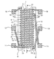
- FIG. 5 is a top view schematically showing the fluxgate magnetic element according to the first embodiment of the present invention.
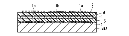
- FIG. 6 is a cross-sectional view taken along line a-a ′ in FIG. 7A to 7E are front sectional views showing manufacturing steps taken along line b-b 'in FIG.
- the flux gate type magnetic element M ⁇ b> 12 includes a magnetic core 1, a first wiring layer 4, a first insulating layer 5, and a second insulation. It has the layer 6, the 2nd wiring layer 7, the opening part 8, and the board
- the first wiring layer 4 and the second wiring layer 7 constitute an exciting coil (solenoid coil) 9, a detection coil (solenoid coil) 10, and a feedback coil (solenoid coil) 21 wound around the magnetic core 1.
- the planar shape of the magnetic core 1 is a shape having a longitudinal direction, and the cross-sectional shape thereof is a thin film shape formed by depositing a magnetic material.
- the excitation coil 9, the detection coil 10, and the feedback coil 21 are formed over the entire length of the magnetic core 1 in the longitudinal direction. And it is wound as a triple helix so that each wiring may become substantially parallel.
- FIGS. 7A to 7E A method for forming a fluxgate magnetic element according to the present embodiment will be described with reference to FIGS. 7A to 7E.
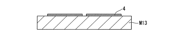
- the first wiring layer 4 for forming the lower wiring of the solenoid coil is formed on the nonmagnetic substrate M13.
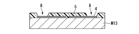
- FIG. 7B the magnetic core 1 and the first insulating layer 5 for insulating the solenoid coil are formed on the first wiring layer 4.
- the first insulating layer 5 is provided with an opening 8 at a portion where the first wiring layer 4 is connected to the second wiring layer 7 which will be an upper wiring of a solenoid coil to be formed later.
- the magnetic core 1 made of a soft magnetic film is formed on the first insulating layer 5.
- FIG. 7A the first wiring layer 4 for forming the lower wiring of the solenoid coil is formed on the nonmagnetic substrate M13.
- FIG. 7B the magnetic core 1 and the first insulating layer 5 for insulating the solenoid coil are formed on the first wiring layer 4.
- the second insulating layer 6 in which the opening 8 is provided in the connection portion between the first wiring layer 4 and the second wiring layer 7 is formed.
- a second wiring layer 7 is formed on the second insulating layer 6 so as to connect adjacent wirings of the first wiring layer 4 at their end portions, and the solenoid coil is Forming. Since the wiring is connected to every two adjacent wirings, the loop of the solenoid coil in the cross section is not closed.
- An exciting coil 9, a detection coil 10, and a feedback coil 21 are provided by a solenoid coil formed by the first wiring layer 4 and the second wiring layer 7. These are each wound around the magnetic core 1 independently. Electrode pads 11 for connection to the outside are formed at both ends of the detection coil 10. Electrode pads 12 for connecting to the outside are formed at both ends of the exciting coil 9. Electrode pads 13 for connecting to the outside are formed at both ends of the feedback coil 21.
- the electrode pad 11 is connected to a terminal to the sense amplifier MT12, the electrode pad 12 is connected to a terminal to the excitation current generating circuit MT11, and the electrode pad 13 is connected to a terminal to the current amplifier MT15.
- the excitation coil 9, the detection coil 10, and the feedback coil 21 can all be symmetrical with the same number of turns.
- the feedback coil 21 is wound over the entire length of the magnetic core 1 so that the pitch is uniform.
- the magnetic core 1 is excited by energizing the exciting coil 9 wound around it. When the magnetization direction of the magnetic core 1 is reversed, an induced voltage is generated in the detection coil 10.
- the magnetic core 1 is excited by energizing the exciting coil 9 from the outside with a triangular wave current that changes with time through the electrode pad 12, and the generated magnetic field is inverted to cause the detection coil 10 to have a pulse shape.
- An induced voltage is generated.
- the induced voltage generated in the detection coil 10 is output to the control integrated circuit MT10 via the electrode pad 11. Then, signal processing proceeds inside the control integrated circuit MT10 and is applied to the feedback coil 21 through the electrode pad 13 as a feedback current.
- the flux gate type magnetic element shown in FIG. 14 may be used.
- the planar shape of the magnetic core 1 is such that the central portion in the longitudinal direction is constricted, and both end portions 1a are formed wider than the central portion 1b.
- a detection coil 10 is wound around the central portion of the magnetic core 1
- an excitation coil 9 is wound around the wide end portions 1a.
- a feedback coil 21 is wound over the entire length of the magnetic core 1. And it is wound as a triple helix so that each wiring may become substantially parallel.
- FIGS. 5 and 14 hatching is added to identify the coils.
- the configuration other than the magnetic other core 1, the coils 9, 10, 21 and the electrode pads 11, 12, 13 is omitted.
- the magnetic sensor M10 may have a demagnetizing body M11.
- the magnetic sensor M10 includes a demagnetizing body M11 made of a chip-like soft magnetic body mounted on a package M10a, a flux gate type thin film magnetic element M12 having a magnetic core 1 formed on a nonmagnetic substrate M13, It consists of a bonding wire M15 that electrically connects the lead frame M14 and the magnetic element M12.
- the magnetic element M12 is stacked and mounted on a plate-like demagnetizing body (chip-shaped soft magnetic body) M11.
- the magnetic sensing direction of the magnetic sensor M10 is parallel to the surface of the substrate M13.
- a metal soft magnetic material such as NiFe, a Co-based amorphous material, a no-milk-like soft magnetic material such as ferrite, or a sheet-like soft magnetic material can be used.
- the demagnetizing body M11 is provided at a position separated from the surface of the magnetic core, which will be described later, to reduce the external magnetic field Hext flowing into the first magnetic body, and the substrate M13 is an external magnetic field flowing into the magnetic core 1.
- the distance setting unit sets the distance between the magnetic element M12 and the demagnetizing body M11.
- the distance setting unit is integrated with the magnetic element M12.
- the distance between the demagnetizing body M11 and the magnetic element M12 is set by the thickness of the substrate M13.
- the demagnetizing body M11 is desirably formed so as to cover an area wider than the magnetic element M12 in the longitudinal direction of the magnetic element M12 in plan view. Thereby, most of the external magnetic field Hext is absorbed by the demagnetizing body M11, and only a part of the component of the external magnetic field Hext is applied to the magnetic core 1 of the magnetic element M12.
- a feedback magnetic field Hfb is applied from the feedback coil 21 to the magnetic core 1 so as to be equal. Accordingly, when the external magnetic field Hext is large enough to saturate the magnetic core 1 or when the linearity of the BH curve of the magnetic core 1 is disturbed in a region where the external magnetic field Hext is away from the zero point.
- the external magnetic field Hext can be measured in a highly linear state by eliminating these effects.
- the magnetic sensor MS10 corresponding to a wide range of magnetic field strengths can be obtained without depending on the structure of the magnetic element M12 (such as the size of the magnetic core and coil wiring).
- the only factors that determine the value of the feedback current are the period T of the triangular wave current supplied to the exciting coil 9 and the feedback magnetic field Hfb created by the exciting coil 9 and the exciting magnetic field and the feedback coil 21. Hardly contributes. Therefore, the influence of the characteristics of the element itself can be greatly reduced as compared with the conventional magnetic sensor.
- the magnetic field strength output could only be intermittently output at a time interval set by a multiple of a counter longer than the period T of the triangular wave current flowing through the exciting coil 9, but according to the present embodiment, the output is continuous.
- the magnetic field strength can be output, and the measurement accuracy as a magnetic sensor can be improved.
- the output by the counter is performed at a cycle of about 1 mSec, in this embodiment, it is possible to output analog values continuously with almost no time lag.
- the magnetic element M12 and the control integrated circuit MT10 are both arranged one by one.
- a plurality of magnetic elements M12 may be used, and in this case, the control integrated circuit is used.
- the number of magnetic elements can be accommodated by increasing MT10 or using a multiplexer. In that case, it is possible to make the measurement more accurate by performing calculations using a plurality of outputs such as referring to the measurement results of the plurality of magnetic elements M12.
- the flux gate type magnetic element of the present invention can be used as a small magnetic sensor, and the magnetic sensor is widely used as an electronic azimuth meter in a mobile phone, a portable navigation device, a game controller and the like.
- Examples of utilization of the present invention include ammeters for large currents such as automobile drive systems and input / output lines to storage batteries.
Landscapes
- Physics & Mathematics (AREA)
- Condensed Matter Physics & Semiconductors (AREA)
- General Physics & Mathematics (AREA)
- Measuring Magnetic Variables (AREA)
Abstract
非磁性の基板上に形成されたフラックスゲート型磁気素子は、磁性体コアと、前記磁性体コアに巻き回された励磁コイルと、前記磁性体コアに巻き回された検出コイルと、前記磁性体コアに巻き回されたフィードバックコイルと、を備える。
Description
本発明は、磁界強度の測定方法、フラックスゲート型磁気素子および磁気センサに関する。
本願は、2012年3月30日に、日本に出願された特願2012-083253号に基づき優先権を主張し、その内容をここに援用する。
本願は、2012年3月30日に、日本に出願された特願2012-083253号に基づき優先権を主張し、その内容をここに援用する。
従来、磁界の強度を測定するための磁気素子として、フラックスゲート型磁気素子が知られている。フラックスゲート型磁気素子は、小型で感度が高いという特徴を備えており、地磁気を測定する電子コンパスや、電流が作る磁界強度を測定して電流値に換算する電流センサとして用いられている。
従来のフラックスゲート型磁気素子の一例として、特許文献1に開示されているフラックスゲート型磁気素子がある。特許文献1のフラックスゲート型磁気素子は、薄膜状の磁性体コアに励磁用コイルと検出コイルが巻回されている。
特許文献1のフラックスゲート型磁気素子は、以下の検出原理により磁界強度を出力する。
まず、磁性体コア材に巻回した励磁用コイルに、一定周期で変動する三角波励磁電流を印加する。その三角波励磁電流によって生じた三角波状の励磁磁界により、磁性コアはB-Hカーブに沿って磁化飽和と磁化方向の反転を繰り返す。この磁化方向が反転するときにパルス状の電圧信号が検出コイルに発生する。
ここに、被測定磁界である外部磁界が印可されたとする。三角波励磁電流によって発生した励磁磁界に外部磁界が足し合わされるため、外部磁界の大きさの分だけパルス電圧信号が発生するタイミングはシフトする。そのパルス電圧信号が発生する時間変化を検出回路で取り出すことによって、外部磁界の大きさに応じた出力を得ることができる。
特許文献1のフラックスゲート型磁気素子は、以下の検出原理により磁界強度を出力する。
まず、磁性体コア材に巻回した励磁用コイルに、一定周期で変動する三角波励磁電流を印加する。その三角波励磁電流によって生じた三角波状の励磁磁界により、磁性コアはB-Hカーブに沿って磁化飽和と磁化方向の反転を繰り返す。この磁化方向が反転するときにパルス状の電圧信号が検出コイルに発生する。
ここに、被測定磁界である外部磁界が印可されたとする。三角波励磁電流によって発生した励磁磁界に外部磁界が足し合わされるため、外部磁界の大きさの分だけパルス電圧信号が発生するタイミングはシフトする。そのパルス電圧信号が発生する時間変化を検出回路で取り出すことによって、外部磁界の大きさに応じた出力を得ることができる。
従来のフラックスゲート型磁気素子には、次に説明するような問題点があった。
フラックスゲート型磁気素子の磁性体コアは、図4の破線で示すようなB-H曲線の磁気飽和特性を有している。このB-H曲線では、グラフの原点を中心対称として、磁性体コアに印加される磁界Hと磁性体コアの磁束密度Bとの関係が直線的に変化する領域を有している。フラックスゲート型磁気素子は、この直線領域の磁気飽和特性を利用して磁界強度を測定する。
一般的な磁性材料で形成された磁性体コアにおいては、外部磁界が印加されると、磁性体コアの磁気飽和特性が変化し、図4の実線で示すようにB-H曲線における直線領域のリニアリティ(直線性)も変化する。すなわち、外部磁界が印加されることによって、磁界Hと磁束Bとの関係性が乱れた状態となる。さらに、その乱れの度合いは、印加される外部磁界のレンジに応じて異なっており、大きな外部磁界が印加されるほど、B-H曲線のリニアリティも悪化する度合いも大きくなる。
上記の理由により、前述した検出コイルに発生するパルス状の電圧信号が発生するタイミングが外部磁界のレンジによって変化し、特に大きな磁界が印加される場合において、高精度に磁気強度を測定することが困難であった。
フラックスゲート型磁気素子の磁性体コアは、図4の破線で示すようなB-H曲線の磁気飽和特性を有している。このB-H曲線では、グラフの原点を中心対称として、磁性体コアに印加される磁界Hと磁性体コアの磁束密度Bとの関係が直線的に変化する領域を有している。フラックスゲート型磁気素子は、この直線領域の磁気飽和特性を利用して磁界強度を測定する。
一般的な磁性材料で形成された磁性体コアにおいては、外部磁界が印加されると、磁性体コアの磁気飽和特性が変化し、図4の実線で示すようにB-H曲線における直線領域のリニアリティ(直線性)も変化する。すなわち、外部磁界が印加されることによって、磁界Hと磁束Bとの関係性が乱れた状態となる。さらに、その乱れの度合いは、印加される外部磁界のレンジに応じて異なっており、大きな外部磁界が印加されるほど、B-H曲線のリニアリティも悪化する度合いも大きくなる。
上記の理由により、前述した検出コイルに発生するパルス状の電圧信号が発生するタイミングが外部磁界のレンジによって変化し、特に大きな磁界が印加される場合において、高精度に磁気強度を測定することが困難であった。
本発明は、フラックスゲート型磁気素子において、大きな外部磁界が印加されたとしても、高精度に磁界強度を測定することが可能な磁界強度の測定方法、フラックスゲート型磁気素子および磁気センサを提供する。
本発明の第1様態に係るフラックスゲート型磁気素子は、非磁性の基板上に形成されたフラックスゲート型磁気素子であって、磁性体コアと、前記磁性体コアに巻き回された励磁コイルと、前記磁性体コアに巻き回された検出コイルと、前記磁性体コアに巻き回されたフィードバックコイルと、を備える。
本発明の第1様態に係るフラックスゲート型磁気素子によれば、フィードバックコイルが設けられているため、磁性体コアにおける被測定磁界を打ち消すようなフィードバック磁界を印加することができる。そのため、磁性体コアにおける実効的な磁界強度を軽減させることが可能となり、磁性体コアの磁気飽和特性を示すB-H曲線の直線性が良好な状態の磁気飽和特性を利用した磁界強度の測定が行われる。したがって、高精度に磁界強度を測定することが可能なフラックスゲート型磁気素子を提供することができる。
本発明の第2様態に係る磁気センサは、磁性体コアと、前記磁性体コアに巻き回された第1のソレノイドコイルおよび第2のソレノイドコイルと、を備え、前記第1のソレノイドコイルおよび第2のソレノイドコイルの何れか一方が励磁コイルとされ他方が検出コイルとされ、前記磁性体コアに巻き回されたフィードバックコイルを有するフラックスゲート型磁気素子と、前記磁性体コアにおける被測定磁界を打ち消すフィードバック磁界を発生させるように、前記フィードバックコイルにフィードバック電流を供給するとともに、該フィードバック電流の値に基づいて被測定磁界の強度を出力する制御用集積回路と、を具える。
本発明の第2様態に係る磁気センサによれば、磁性体コアにおける被測定磁界を打ち消すようにフィードバックコイルからフィードバック磁界が印加されるので、大きな被測定磁界が印加されたとしても、磁性体コアにおける実効的な磁界強度を軽減させることができる。そのため、磁性体コアの磁気飽和特性を示すB-H曲線において、直線性の良好な状態の磁気飽和特性を利用した磁界強度の測定が行われ、高精度に磁界強度を測定することができる。これにより、磁性体コアの磁気特性に因ることなく測定する磁界強度の範囲を規制されることなく、磁気素子としてのリニアリティ(直線性)を維持した出力を得ることが可能となる。
本発明の第3様態に係る磁界強度の測定方法は、磁性体コアと、前記磁性体コアに巻き回された励磁コイル、検出コイルおよびフィードバックコイルと、を備えたフラックスゲート型磁気素子を用いた磁界強度の測定方法であって、前記フィードバックコイルは、前記磁性体コアにおける被測定磁界を打ち消すフィードバック磁界を発生させ、前記フラックスゲート型磁気素子は、前記フィードバックコイルに供給する電流の値に基づいて被測定磁界の強度を出力する。
本発明の第3様態に係る磁界強度の測定方法によれば、磁性体コアにおける被測定磁界を打ち消すようにフィードバックコイルからフィードバック磁界が印加されるので、大きな被測定磁界が印加されたとしても、磁性体コアにおける実効的な磁界強度を軽減させることができる。そのため、磁性体コアの磁気飽和特性を示すB-H曲線のリニアリティが変化せず、直線性の良好な磁気飽和特性を利用した磁界強度の測定が行われ、高精度に磁界強度を測定することができる。
本発明の第4様態に係る磁界強度の測定方法は、第3様態に係る磁界強度の測定方法において、前記フィードバック磁界の強度は、被測定磁界の磁界強度と略同一であってもよい。
本発明の第4様態に係るフラックスゲート型磁気素子を用いた磁界強度の測定方法によれば、磁性体コアに実効的に印加される磁界がほぼゼロとなり、B-H曲線において最も直線性の良好な状態の磁気飽和特性を利用した磁界強度の測定が行われ、より高精度に磁界強度を測定することができる。
本発明の第5様態に係る磁界強度の測定方法は、第3様態または第4様態に係る磁界強度の測定方法において、前記フィードバックコイルに供給する電流の電流値は、前記検出コイルからの出力に基づいて決定されてもよい。
本発明の第5様態に係るフラックスゲート型磁気素子を用いた磁界強度の測定方法によれば、検出コイルからの出力に基づいてフィードバックコイルに供給される電流の値が決定されるので、磁性体コアの磁気特性に因ることなく、磁気素子としてのリニアリティ(直線性)を維持した出力を得ることが可能となる。
本発明の第1様態に係るフラックスゲート型磁気素子によれば、フィードバックコイルが設けられているため、磁性体コアにおける被測定磁界を打ち消すようなフィードバック磁界を印加することができる。そのため、磁性体コアにおける実効的な磁界強度を軽減させることが可能となり、磁性体コアの磁気飽和特性を示すB-H曲線の直線性が良好な状態の磁気飽和特性を利用した磁界強度の測定が行われる。したがって、高精度に磁界強度を測定することが可能なフラックスゲート型磁気素子を提供することができる。
以下、本発明の第1実施形態に係る磁気センサを、図面に基づいて説明する。
図1は、本発明の第1実施形態に係る磁気センサを示す模式図である。図1において、符号MS10は磁気センサを示している。
図1は、本発明の第1実施形態に係る磁気センサを示す模式図である。図1において、符号MS10は磁気センサを示している。
本発明の第1実施形態に係る磁気センサMS10は、図1に示すように、フラックスゲート型磁気素子M12と、制御用集積回路(信号処理回路)MT10と、を備える。
フラックスゲート型磁気素子M12は、軟磁性材料からなる磁性体コア1に巻回された励磁コイル9、検出コイル10、フィードパックコイル21、を有する。
制御用集積回路MT10は、励磁電流発生回路MT11、センスアンプMT12、コンパレータMT13、フィードバック制御回路(FB制御回路)MT14、電流アンプMT15、出力端子MT16を有する。
磁気センサMS10は、例えば導電路に流れる電流が作る被測定磁界を測定するための電流センサなどである。
フラックスゲート型磁気素子M12は、軟磁性材料からなる磁性体コア1に巻回された励磁コイル9、検出コイル10、フィードパックコイル21、を有する。
制御用集積回路MT10は、励磁電流発生回路MT11、センスアンプMT12、コンパレータMT13、フィードバック制御回路(FB制御回路)MT14、電流アンプMT15、出力端子MT16を有する。
磁気センサMS10は、例えば導電路に流れる電流が作る被測定磁界を測定するための電流センサなどである。
励磁コイル9は、励磁電流発生回路MT11に接続される。後述するように連続波形とされる励磁電流信号が励磁コイル9に供給される。
検出コイル10は、センスアンプMT12に接続される。センスアンプMT12では、検出コイル10からの出力信号が増幅される。センスアンプMT12は、コンパレータMT13に接続される。コンパレータMT13は、フィードバック制御回路MT14に接続される。フィードバック制御回路MT14は、電流アンプMT15に接続される。電流アンプMT15はは、フィードパックコイル21および出力端子MT16に接続される。
検出コイル10は、センスアンプMT12に接続される。センスアンプMT12では、検出コイル10からの出力信号が増幅される。センスアンプMT12は、コンパレータMT13に接続される。コンパレータMT13は、フィードバック制御回路MT14に接続される。フィードバック制御回路MT14は、電流アンプMT15に接続される。電流アンプMT15はは、フィードパックコイル21および出力端子MT16に接続される。
励磁電流発生回路MT11が発生させる三角波の励磁電流が励磁コイル9に供給され、それに伴い励磁磁界が磁性体コア1に発生する。磁性体コア1に発生した励磁磁界は、正負交互に磁界の向きが変動する。検出コイル10においては、磁界の向きが切り替わるタイミングでパルス状の誘導電圧信号(検出信号)が発生する。検出コイル10に発生したパルス状の誘導電圧信号(検出信号)は、検出コイル10に接続された端子を通してセンスアンプMT12へ入力される。センスアンプMT12は、この検出信号を後段のコンパレータMT13が動作可能な程度まで増幅する。
コンパレータMT13には、センスアンプMT12で増幅された検出信号が入力される。コンパレータMT13は、この増幅された検出信号の電圧値と、予め定められた閾値電圧値とを比較し、その結果に応じてHigh値またはLow値の信号を出力する。このように、コンパレータMT13は、検出信号をPWM(Pulse Width Modulation)波形に変換する。
コンパレータMT13が出力したHigh値の維持時間とLow値の維持時間の比は、Duty比と呼ばれる。このDuty比が50:50であれば外部磁界(被測定磁界)が印加されていない状態である。50:50から外れていれば、外部磁界(被測定磁界)が印加されている状態である。50:50から大きく外れるほど、大きな外部磁界(被測定磁界)が印加されていることを示す。
コンパレータMT13が出力したHigh値の維持時間とLow値の維持時間の比は、Duty比と呼ばれる。このDuty比が50:50であれば外部磁界(被測定磁界)が印加されていない状態である。50:50から外れていれば、外部磁界(被測定磁界)が印加されている状態である。50:50から大きく外れるほど、大きな外部磁界(被測定磁界)が印加されていることを示す。
フィードバック制御回路MT14は、コンパレータMT13からの出力であるHigh値の維持時間とLow値の維持時間のDuty比が50:50からずれた場合に、そのずれ量に応じた値の直流電圧信号を出力する。
電流アンプMT15は、フィードバック制御回路MT14が出力した直流電圧信号を基にして、Duty比を50:50に近づけるためのフィードパック電流をフィードバックコイル21に供給する。これにより、磁性体コアにおける磁化状態は、実効的には外部磁界が印可されていない状態となる。
電流アンプMT15は、フィードバック制御回路MT14が出力した直流電圧信号を基にして、Duty比を50:50に近づけるためのフィードパック電流をフィードバックコイル21に供給する。これにより、磁性体コアにおける磁化状態は、実効的には外部磁界が印可されていない状態となる。
本発明の第1実施形態の磁界強度の測定方法を、磁気センサMS10を構成するフラックスゲート型磁気素子M12等の動作原理を通して説明する。
図2は、フラックスゲート型磁気素子の動作原理を示すグラフである。図2(a)は、励磁コイルに供給する三角波励磁電流の時間変化を示すグラフである。図2(b)は、コアの磁化状態の時間変化を示すグラフである。図2(c)は、検出コイルに生じる検出信号の時間変化を示すグラフである。図3は、フラックスゲート型磁気素子M12の磁性体コアの磁化状態の時間による変化を示すB-H曲線(ヒステリシス曲線)である。
図2は、フラックスゲート型磁気素子の動作原理を示すグラフである。図2(a)は、励磁コイルに供給する三角波励磁電流の時間変化を示すグラフである。図2(b)は、コアの磁化状態の時間変化を示すグラフである。図2(c)は、検出コイルに生じる検出信号の時間変化を示すグラフである。図3は、フラックスゲート型磁気素子M12の磁性体コアの磁化状態の時間による変化を示すB-H曲線(ヒステリシス曲線)である。
励磁電流発生回路MT11から、図2(a)に示すような三角波励磁電流を励磁コイル9に供給すると、励磁コイル9の作る励磁磁界Hexcにより磁性体コア1に励磁磁界が生じる。図2(a)の横軸は時間を、縦軸は電流値を示す。磁性体コア1は、図3に示すような磁気飽和特性を有するため、磁性体コア1における磁化状態は、図2(b)に示すような時間変化をする。図2(b)の横軸は時間を、縦軸は磁性体コア1における磁束密度Bを示す。検出コイル10には、磁性体コア1の磁化状態の極性が反転するタイミング、すなわち時間変化dB/dtが存在するタイミングにおいて、磁性体コア1の断面積S、ピックアップコイル10の巻き数Nに比例した誘導電圧Vpu=NS×dB/dtが生じる。検出コイル10に発生する誘導電圧Vpuは、図2(c)に示すような時間変化をするパルス状の誘導電圧信号(検出信号)である。図2(c)の横軸は時間を、縦軸は電圧値を示す。磁性体コア1の磁束密度Bの時間変化dB/dtが大きいほど、誘導電圧信号の波高値は高くなり、パルス幅は狭くなり、より急峻なパルス状波形の誘導電圧信号が得られる。図2(c)における時間間隔t1は、外部磁界(被測定磁界)Hext、磁性体コア1の磁束密度Bが増加する時と減少する時との磁場の強さHのずれHc、励磁コイル9の作る磁界Hexc、三角波励磁電流の周期T及びコイルのインダクタンスによる遅延時間Tdを用いて、式(1)のように表される。

同様に、図2の(c)における時間間隔t2は、式(2)のように表される。

式(1)及び式(2)より、外部磁界によって生ずる時間間隔の変化量t2-t1は、式(3)のように表される。

式(3)より、外部磁界によって生ずる時間間隔の変化t2-t1は、外部磁界Hextと励磁コイル9の作る励磁磁界Hexcの比 Hext/Hexc および三角波励磁電流の周期Tに依存することがわかる。外部磁界に対する感度S=d(t2-t1)/dHextは、励磁コイル9に通電する三角波励磁電流の振幅Iexc、励磁コイル9に流れる三角波励磁電流の単位電流当たりの発生磁界(励磁効率α)、及び三角波励磁電流の周期Tを用いて、S=T/(2・Iexc×α)で表される。よって、三角波励磁電流の振幅Iexcが大きいほど、フラックスゲート型磁気素子M12の感度Sは小さくなる。そして、三角波励磁電流の周期Tが大きいほど、フラックスゲート型磁気素子の感度Sは大きくなる。
励磁効率αは、フラックスゲート磁気素子M12を構成する磁性体コア1と励磁コイル9の巻き数によって決定される値である。励磁効率αが大きいほど、同一感度で同一の磁界範囲を測定しようとした場合には、少ない電流でフラックスゲート磁気素子M12を駆動することができる。また、式(3)において、外部磁界Hext=励磁磁界Hexcとなるとき式(3)は0となり、このときの外部磁界Hextが測定可能な磁界範囲の上限となる。Hexc=α×Iexcで表されることから、励磁効率αが大きいほど、同一の電流で駆動した場合に広い測定可能な磁界範囲を有するフラックスゲート型磁気素子となる。
この励磁効率αは、励磁コイル9に三角波励磁電流を通電することにより磁性体コア1に発生する磁束密度と、外部磁界により磁性体コア1に発生する磁束密度との比率を示すものである。励磁効率αは、磁性体コア1のヒステリシス曲線の非飽和領域における磁気密度Bの外部磁界Hextに対する傾きdB/dHextと、同じく磁性体コア1の磁束密度Bの励磁コイルに流れる三角波励磁電流Iexcに対する傾きdB/dIexcとの比率により決まり、式(4)で表される。

すなわち、上記のように磁気センサMS10は、制御用集積回路(信号処理回路)MT10の励磁電流発生回路MT11から励磁コイル9へ、連続して振動する三角波形の励磁電流を供給し、磁性体コア1における磁束の向きが連続的に振動して飽和する磁場を発生させる。磁性体コア1内においては、磁束の向きが反転するタイミングでパルス状の誘導電圧が検出コイル10にて発生する。この検出コイル10から出力されたパルス状の誘導電圧信号の時間間隔T0を、外部磁界Hextが印加されていない場合と印加されている場合とにおける差異が最小となるように、磁性体コア1に巻回されたフィードバックコイル21にフィードバック電流を供給する。
より具体的な動作原理を図10~図12を用いて説明する。
(外部磁界Hext=0の場合)
図10(a)に示すように、励磁電流発生回路MT11は、周期Tで変動する三角波励磁電流を励磁コイル9に供給する。それに伴って磁性体コア1において励磁磁界が発生する。図10(b)は、磁性体コア1における磁化状態の時間変化を示す。外部磁界Hext=0であるため、磁性体コア1における磁化状態は励磁磁界のみの影響を受け、三角波励磁電流と同期して変動する。したがって、三角波電流の極性が反転する時刻t2、t4、t6、t8と同じタイミングで、磁性体コア1における磁化状態(磁化方向)が反転する。図10(c)は、磁性体コア1の磁化状態が反転するときに検出コイル10に発生するパルス状の誘導電圧信号を示す。磁性体コア1の磁化状態が負から正へ反転する時刻t2とt6においては、正符号の誘導電圧信号K+が発生する。磁性体コア1の磁化状態が正から負へ反転する時刻t4とt8においては、負符号の誘導電圧信号K-が発生する。
図10(a)に示すように、励磁電流発生回路MT11は、周期Tで変動する三角波励磁電流を励磁コイル9に供給する。それに伴って磁性体コア1において励磁磁界が発生する。図10(b)は、磁性体コア1における磁化状態の時間変化を示す。外部磁界Hext=0であるため、磁性体コア1における磁化状態は励磁磁界のみの影響を受け、三角波励磁電流と同期して変動する。したがって、三角波電流の極性が反転する時刻t2、t4、t6、t8と同じタイミングで、磁性体コア1における磁化状態(磁化方向)が反転する。図10(c)は、磁性体コア1の磁化状態が反転するときに検出コイル10に発生するパルス状の誘導電圧信号を示す。磁性体コア1の磁化状態が負から正へ反転する時刻t2とt6においては、正符号の誘導電圧信号K+が発生する。磁性体コア1の磁化状態が正から負へ反転する時刻t4とt8においては、負符号の誘導電圧信号K-が発生する。
検出コイル10に発生した誘導電圧信号(K+、K-)は、フラックスゲート型磁気素子M12の出力として制御用集積回路MT10に入力される。まず、センスアンプMT12において誘導電圧信号が増幅され、続いてコンパレータMT13に入力される。コンパレータMT13は、図10(d)に示すように、増幅された誘導電圧信号をPWM(Pulse Width Modulation)波形へと変調する。すなわち、増幅された誘導電圧信号の電圧値と予め定められた閾値電圧値とを比較し、増幅された誘導電圧信号の電圧値の方が大きい場合はHighが維持され、増幅された誘導電圧信号の方が小さい場合はLowが維持された電圧信号を出力する。Highが維持される時間幅をTH、Lowが維持される時間幅をTLとすると、外部磁界Hext=0である場合においてはTH=TLとなり、これが基準時間間隔T0(ゼロ)とされる。基準時間間隔T0は、三角波電流の半周期T/2と等しい。Highの時間幅(TH)とLowの時間幅(TL)とのDuty比は、T0:T0(=50:50)となる。
コンパレータMT13において変調された信号は、LPF(ローパスフィルタ)フィードバック制御回路14へ入力される。信号は、フィードバック制御回路MT14、電流アンプMT15を経てフィードバック電流としてフィードバックコイル21に出力されるとともに、電流アンプMT15からの出力値が出力端子MT16から外部磁界強度の指標を表す磁気センサの出力として連続的に出力される。この出力が、外部磁界Hext=0における出力となる。
(外部磁界Hext>0の場合)
図10(a)に示す外部磁界Hext=0の場合と同様に、図11(a)に示した三角波電流が励磁コイル9に供給されると、磁性体コア1に励磁磁界が発生する。磁性体コア1における磁化状態は、励磁磁界に加えて外部磁界Hextの影響を受ける。そのため、磁性体コア1における磁化状態の時間変化を示すグラフは、図11(b)に示すように、図10(b)の波形が一方の側(図11(b)では負の側)へシフトした形状となる。そうすると、磁性体コア1における磁化状態(磁化方向)が反転するタイミングが、励磁コイル9の三角波電流の変動と同期しなくなる。例えば、磁性体コアの磁化方向が負から正へ反転するタイミングが、時刻t2、t6からシフトとして、それぞれ時刻t3、t7へ近づく。そのため、正符号のパルス状誘導電圧信号K+が発生するタイミングも、時刻t3、t7へ近づく(図11(c))。一方、磁性体コア1の磁化方向が正から負へ反転するタイミングが、時刻t4、t8からシフトして、それぞれ時刻t3、t7へ近づく。そのため、負符号のパルス状の誘導電圧信号K-が発生するタイミングも、時刻t3、t7へ近づく(図11(c))。
図10(a)に示す外部磁界Hext=0の場合と同様に、図11(a)に示した三角波電流が励磁コイル9に供給されると、磁性体コア1に励磁磁界が発生する。磁性体コア1における磁化状態は、励磁磁界に加えて外部磁界Hextの影響を受ける。そのため、磁性体コア1における磁化状態の時間変化を示すグラフは、図11(b)に示すように、図10(b)の波形が一方の側(図11(b)では負の側)へシフトした形状となる。そうすると、磁性体コア1における磁化状態(磁化方向)が反転するタイミングが、励磁コイル9の三角波電流の変動と同期しなくなる。例えば、磁性体コアの磁化方向が負から正へ反転するタイミングが、時刻t2、t6からシフトとして、それぞれ時刻t3、t7へ近づく。そのため、正符号のパルス状誘導電圧信号K+が発生するタイミングも、時刻t3、t7へ近づく(図11(c))。一方、磁性体コア1の磁化方向が正から負へ反転するタイミングが、時刻t4、t8からシフトして、それぞれ時刻t3、t7へ近づく。そのため、負符号のパルス状の誘導電圧信号K-が発生するタイミングも、時刻t3、t7へ近づく(図11(c))。
その結果、コンパレータMT13において変調されたあとのHighの時間幅THとLowの時間幅TLも変化し、図11(d)に示すうようにTH<TLとなる。このときのTHをT1とし、TLをT2とすると、T1は基準時間間隔T0よりも小さくなり、T2は基準時間間隔T0よりも大きくなる。この基準時間間隔T0とT1、T2との差分だけ、外部磁界Hextの影響をキャンセルするような、つまり外部磁界Hextと逆方向の磁界を発生させるように、電流アンプMT15からフィードバックコイル21にフィードバック電流が供給される。フィードバックコイル21は、外部磁界Hextをキャンセルするような方向と大きさを有するフィードバック磁界Hfbを発生させるので、磁性体コア1における外部磁界Hextは低減され、外部磁界Hext=0の付近の磁場状態が維持される。
これを、B-H曲線を用いて説明すると、外部磁界Hext>0が印可されたとしても、磁性体コア1の磁化状態はB-H曲線のリニアリティ(直線性)が低下した状態へと変化せず、リニアリティの良好な状態の磁気飽和特性を利用した磁気強度の測定が可能となる。したがって、大きな外部磁界が印可されたとしても、フィードバック磁界によって磁性体コアにおける実効的な磁化状態は、外部磁界Hext=0の状態へと近づき、リニアリティの良好なB-H曲線を利用した磁界強度の測定を行うことができる。
なお、電流アンプMT15からの出力は、端子MT16を通して外部磁界強度表す磁気センサの出力として連続的に出力される。
なお、電流アンプMT15からの出力は、端子MT16を通して外部磁界強度表す磁気センサの出力として連続的に出力される。
(外部磁界Hext<0の場合)
図12(a)(図10(a)、図11(a)と同じ)に示した三角波電流が励磁コイル9に供給されると、磁性体コア1に励磁磁界が発生する。磁性体コア1における磁化状態は、励磁磁界に加えて外部磁界Hextの影響を受ける。上述した外部磁界Hext>0の場合とは逆の作用が働くため、コンパレータMT13において変調された後のHighの時間幅THとLowの時間幅TLは、図12(d)に示すように、TH>TLとなる。このときのTHをT3とし、TLをT4とすると、T3は基準時間間隔T0よりも大きくなり、T4は基準時間間隔T0よりも小さくなる。この基準時間間隔T0と、T3およびT4との差分だけ外部磁界Hextをキャンセルするような、つまり外部磁界Hextと逆方向の磁界を発生させるように、電流アンプMT15からフィードバックコイル21にフィードバック電流21が供給される。フィードバックコイル21は、外部磁界Hextをキャンセルするような方向と大きさを有するフィードバック磁界Hfbを発生させるので、磁性体コア1における外部磁界Hextをキャンセルし、外部磁界Hext=0付近の磁場状態が維持される。
図12(a)(図10(a)、図11(a)と同じ)に示した三角波電流が励磁コイル9に供給されると、磁性体コア1に励磁磁界が発生する。磁性体コア1における磁化状態は、励磁磁界に加えて外部磁界Hextの影響を受ける。上述した外部磁界Hext>0の場合とは逆の作用が働くため、コンパレータMT13において変調された後のHighの時間幅THとLowの時間幅TLは、図12(d)に示すように、TH>TLとなる。このときのTHをT3とし、TLをT4とすると、T3は基準時間間隔T0よりも大きくなり、T4は基準時間間隔T0よりも小さくなる。この基準時間間隔T0と、T3およびT4との差分だけ外部磁界Hextをキャンセルするような、つまり外部磁界Hextと逆方向の磁界を発生させるように、電流アンプMT15からフィードバックコイル21にフィードバック電流21が供給される。フィードバックコイル21は、外部磁界Hextをキャンセルするような方向と大きさを有するフィードバック磁界Hfbを発生させるので、磁性体コア1における外部磁界Hextをキャンセルし、外部磁界Hext=0付近の磁場状態が維持される。
これを、B-H曲線を用いて説明すると、外部磁界Hext<0が印可されたとしても、磁性体コア1の磁化状態はB-H曲線のリニアリティ(直線性)が低下した状態へと変化せず、リニアリティの良好な磁気飽和特性を利用した磁気強度の測定が可能となる。したがって、大きな外部磁界が印可されたとしても、フィードバック磁界によって磁性体コアにおける実効的な磁化状態は、外部磁界Hext=0の状態へと近づき、リニアリティの良好なB-H曲線を利用した磁界強度の測定を行うことができる。
なお、電流アンプMT15からの出力は、端子MT16を通して外部磁界強度表す磁気センサの出力として連続的に出力される。
なお、電流アンプMT15からの出力は、端子MT16を通して外部磁界強度表す磁気センサの出力として連続的に出力される。
以上のような原理に基づいて、フィードバックバック電流がフィードバックコイル21へと供給される。そして、端子MT16から出力される外部磁界強度の出力信号は、連続変化量であるアナログ値として出力することができる。あるいは、デジタル的にピーク間隔をカウントする手法を用いてもよい。
なお、外部磁界Hextによって変化するパルス信号K+,K-の時間間隔に応じてフィードバック電流を出力したが、このフィードバック電流は、フィードパックコイル21のみならず、励磁コイル9や検出コイル10に流すこともできる。この場合、励磁コイル9に供給する三角波電流や、検出コイルに発生する誘導電圧信号にフィードパック電流の一部を重畳することで実現が可能である。
さらに、フィードバック電流を励磁コイル9や検出コイル10に流した場合には、図9に示すように、フィードバックコイル21を励磁コイル9や検出コイル10と兼用させることができる。この場合、電流アンプMT15のフィードバック端子は、励磁コイル9あるいは検出コイル10に接続される。
さらに、フィードバック電流を励磁コイル9や検出コイル10に流した場合には、図9に示すように、フィードバックコイル21を励磁コイル9や検出コイル10と兼用させることができる。この場合、電流アンプMT15のフィードバック端子は、励磁コイル9あるいは検出コイル10に接続される。
次に、磁気素子M12について説明する。
本実施形態の磁気素子M12は、例えば、phase-delay methodを用いたフラックスゲート型とされてなることができる。磁気素子M12の磁性体コア1の長手方向は、フラックスゲート型の磁気素子M12の感磁方向と一致している。
図5は、本発明の第1実施形態に係るフラックスゲート型磁気素子を概略的に示す上面図である。図6は、図5におけるラインa-a’に沿って切った横断面図である。図7A~図7Eは、図5におけるラインb-b’に沿って切った製造工程を示す正断面図である。
本発明の第1実施形態に係るフラックスゲート型磁気素子M12は、図5,図6に示すように、磁性体コア1と、第1配線層4と、第1絶縁層5と、第2絶縁層6と、第2配線層7と、開口部8と、基板M13とを有する。第1配線層4及び第2配線層7は、磁性体コア1に巻き回された励磁コイル(ソレノイドコイル)9、検出コイル(ソレノイドコイル)10、フィードバックコイル(ソレノイドコイル)21を構成している。
磁性体コア1の平面形状は長手方向を有する形状であり、その断面形状は磁性材料を成膜して形成した薄膜形状である。
励磁コイル9、検出コイル10,フィードバックコイル21は、磁性体コア1の長手方向の全長に亘って形成されている。そして、それぞれの配線が略平行になるように、三重らせんとして巻回されている。
磁性体コア1の平面形状は長手方向を有する形状であり、その断面形状は磁性材料を成膜して形成した薄膜形状である。
励磁コイル9、検出コイル10,フィードバックコイル21は、磁性体コア1の長手方向の全長に亘って形成されている。そして、それぞれの配線が略平行になるように、三重らせんとして巻回されている。
図7A~図7Eを用いて、本実施形態に係るフラックスゲート型磁気素子の形成方法を説明する。
図7Aに示すように、非磁性の基板M13の上に、ソレノイドコイルの下側配線を形成するための第1配線層4が形成される。次に、図7Bに示すように、第1配線層4の上に、磁性体コア1とソレノイドコイルを絶縁するための第1絶縁層5とが形成される。第1絶縁層5には、第1配線層4と後に形成されるソレノイドコイルの上側配線となる第2配線層7とが接続される部分に開口部8が設けられる。
図7Cに示すように、第1絶縁層5の上に軟磁性体膜からなる磁性体コア1が形成される。次に、図7Dに示すように、磁性体コア1の上には、第1配線層4と第2配線層7の接続部に開口部8を設けた第2絶縁層6が形成される。第2絶縁層6の上には、図7Eに示すように、第1配線層4の隣接する配線どうしをその端部にて接続するように第2配線層7が形成されて、ソレノイドコイルを形成している。配線は、2つおきに隣接する配線と接続されるため、断面におけるソレノイドコイルのループは閉じない。
図7Aに示すように、非磁性の基板M13の上に、ソレノイドコイルの下側配線を形成するための第1配線層4が形成される。次に、図7Bに示すように、第1配線層4の上に、磁性体コア1とソレノイドコイルを絶縁するための第1絶縁層5とが形成される。第1絶縁層5には、第1配線層4と後に形成されるソレノイドコイルの上側配線となる第2配線層7とが接続される部分に開口部8が設けられる。
図7Cに示すように、第1絶縁層5の上に軟磁性体膜からなる磁性体コア1が形成される。次に、図7Dに示すように、磁性体コア1の上には、第1配線層4と第2配線層7の接続部に開口部8を設けた第2絶縁層6が形成される。第2絶縁層6の上には、図7Eに示すように、第1配線層4の隣接する配線どうしをその端部にて接続するように第2配線層7が形成されて、ソレノイドコイルを形成している。配線は、2つおきに隣接する配線と接続されるため、断面におけるソレノイドコイルのループは閉じない。
第1配線層4および第2配線層7により形成されたソレノイドコイルによって、励磁コイル9、検出コイル10、フィードバックコイル21が設けられる。これらは、いずれも磁性体コア1に、それぞれ独立に巻き回されている。検出コイル10の両端には、外部と接続するための電極パッド11が形成されている。励磁コイル9の両端には、外部と接続するための電極パッド12が形成されている。フィードバックコイル21の両端には、外部と接続するための電極パッド13が形成されている。電極パッド11はセンスアンプMT12への端子に接続され、電極パッド12は、励磁電流発生回路MT11への端子へ接続され、電極パッド13は電流アンプMT15への端子にそれぞれ接続されている。
ここで、励磁コイル9、検出コイル10及びフィードバックコイル21は、いずれも巻き数が同じで対称とすることができる。特に、フィードバックコイル21は、そのピッチが均一になるように、磁性体コア1の全長にわたって巻回されている。
なお、これらの図は模式的に示されており、各ソレノイドコイルに関しては一部が省略されている。また、磁気素子M12の細部形状は、図に示された形状に限定されるものではない。
ここで、励磁コイル9、検出コイル10及びフィードバックコイル21は、いずれも巻き数が同じで対称とすることができる。特に、フィードバックコイル21は、そのピッチが均一になるように、磁性体コア1の全長にわたって巻回されている。
なお、これらの図は模式的に示されており、各ソレノイドコイルに関しては一部が省略されている。また、磁気素子M12の細部形状は、図に示された形状に限定されるものではない。
磁性体コア1は、その周囲に巻き回された励磁コイル9に通電することにより励磁される。そして、磁性体コア1の磁化方向が反転すると検出コイル10に誘導電圧が発生する。励磁コイル9に対して、電極パッド12を介して時間的に変化する三角波電流を外部より通電することにより磁性体コア1が励磁され、発生した磁界が反転することにより検出コイル10にパルス状の誘導電圧が発生する。検出コイル10に発生した誘導電圧は電極パッド11を介して制御用集積回路MT10に出力される。そして、制御用集積回路MT10の内部において信号処理が進行し、フィードバック電流として電極パッド13を介してフィードバックコイル21に印加される。
本発明の第1実施形態に示したものは一例であり、磁性体コア1,励磁コイル9、検出コイル10及びフィードバックコイル21の配置は、上記の構成に限定されることなく、他の配置とすることができる。特に、励磁コイル9、検出コイル10,フィードバックコイル21は、三重らせん以外の配置も可能である。
例えば、図14に示したフラックスゲート型磁気素子であってもよい。図14に示したフラックスゲート型磁気素子は、磁性体コア1の平面形状は、その長手方向の中央部が括れた形状となっており、両端部1aは中央部1bよりも幅広に形成されている。磁性体コア1の中央部には検出コイル10が巻回されており、幅広な両端部1aには励磁コイル9が巻回されている。そして、磁性体コア1の全長に亘ってフィードバックコイル21が巻回されている。そして、それぞれの配線が略平行になるように、三重らせんとして巻回されている。なお、図5、図14においては、コイルを識別するために、ハッチングを付してある。また、図14においては、磁性他コア1およびコイル9,10,21、電極パッド11,12,13以外の構成は省略した記載となっている。
磁気センサM10は、図8に示すように、減磁体M11を有するものとすることもできる。
この場合、磁気センサM10は、パッケージM10aに実装されたチップ状の軟磁性体からなる減磁体M11と、非磁性基板M13上に形成された磁気コア1を有するフラックスゲート型薄膜磁気素子M12と、リードフレームM14と磁気素子M12を電気的に接続するボンディングワイヤM15から構成される。磁気素子M12は板状の減磁体(チップ状軟磁性体)M11の上に積層して実装されている。磁気センサM10の感磁方向は、基板M13表面と平行方向である。減磁体M11には、例えばNiFeなどの金属軟磁性体材料や、Co系アモルファス等、フェライト等ノミルク状の軟磁性体や、シート状の軟磁性体を用いることができる。
この場合、磁気センサM10は、パッケージM10aに実装されたチップ状の軟磁性体からなる減磁体M11と、非磁性基板M13上に形成された磁気コア1を有するフラックスゲート型薄膜磁気素子M12と、リードフレームM14と磁気素子M12を電気的に接続するボンディングワイヤM15から構成される。磁気素子M12は板状の減磁体(チップ状軟磁性体)M11の上に積層して実装されている。磁気センサM10の感磁方向は、基板M13表面と平行方向である。減磁体M11には、例えばNiFeなどの金属軟磁性体材料や、Co系アモルファス等、フェライト等ノミルク状の軟磁性体や、シート状の軟磁性体を用いることができる。
減磁体M11は、後述する磁気コアの表面から離間した位置に設けられて該第1の磁性体に流入する外部磁界Hextを低減するものとされ、基板M13は、磁気コア1に流入する外部磁界Hextが減磁体M11によって低減する分を制御するために、磁気素子M12と減磁体M11との距離を設定する距離設定部とされる。距離設定部は、磁気素子M12と一体とされている。
減磁体M11と磁気素子M12との距離は、基板M13の厚みにより設定されている。減磁体M11は、平面視して、磁気素子M12の長手方向において、磁気素子M12よりも広い領域を覆うように形成することが望ましい。これにより、外部磁界Hextの大部分は減磁体M11に吸収され、外部磁界Hextの成分のうちの一部のみが磁気素子M12の磁気コア1に印加される。
減磁体M11と磁気素子M12との距離は、基板M13の厚みにより設定されている。減磁体M11は、平面視して、磁気素子M12の長手方向において、磁気素子M12よりも広い領域を覆うように形成することが望ましい。これにより、外部磁界Hextの大部分は減磁体M11に吸収され、外部磁界Hextの成分のうちの一部のみが磁気素子M12の磁気コア1に印加される。
本発明の第1実施形態においては、磁性体コア1の磁化状態は、外部から磁性体コア1に流入する外部磁界(被測定磁界)Hextをキャンセルし、外部磁界Hext=0であるときとほぼ等しい状態となるように、フィードバックコイル21からフィードバック磁界Hfbを磁性体コア1に印加する。したがって、磁性体コア1が飽和してしまう程度に外部磁界Hextが大きい場合や、外部磁界Hextがゼロ点から離れた領域で磁性体コア1のB-H曲線の線形性が乱れている場合にも、これらの影響を排除して、線形性の高い状態で外部磁界Hextの測定をおこなうことができる。このため、磁気素子M12の構造(磁性体コアやコイル配線のサイズなど)に依存することなく、広い範囲の磁界強度に対応した磁気センサMS10とすることが可能である。同時に、フィードバック電流の値を決定する要素が、励磁コイル9に供給する三角波電流の周期Tと励磁コイル9および励磁磁界とフィードバックコイル21が作るフィードバック磁界Hfbのみであり、磁性体コア1の特性は殆ど寄与しない。そのため、従来の磁気センサに比べ、素子自体の特性の影響を非常に小さくできる。
また、従来は励磁コイル9に流す三角波電流の周期Tよりも長いカウンターの倍数で設定された時間間隔によって磁界強度出力を断続的に出力することしかできなかったが、本実施形態により、連続して磁界強度出力をおこなうことが可能になり磁気センサとしての測定精度を向上させることができる。具体的には、カウンターによる出力が1mSec程度の周期でおこなわれていたのに対し、本実施形態では、ほぼタイムラグなくアナログ値を連続して出力することが可能となる。
本発明の第1実施形態は磁気素子M12および制御用集積回路MT10がいずれも1個ずつ配置された例としたが、磁気素子M12を複数用いてもよく、この場合には、制御用集積回路MT10を増やす、マルチプレクサを用いるなどして、磁気素子の数に対応することができる。その場合、複数の磁気素子M12の測定結果を相互に参照するなど複数の出力を用いて演算を行うことで測定をより高精度にすることも可能である。
(実験例1)
実験例1として、図13に示すように、測定する磁界Hextを変化させたときのリニアリティ誤差を算出した。
ここで、リニアリティ誤差Δは、測定出力Houtに対し、
Δ=(Hout-Hext)/Hext ×100(%)
とした。
この結果から、本発明の実施形態に係るフィードバックをおこなう磁気センサにおいては、外部磁界の範囲によらず、リニアリティが向上することがわかる。
実験例1として、図13に示すように、測定する磁界Hextを変化させたときのリニアリティ誤差を算出した。
ここで、リニアリティ誤差Δは、測定出力Houtに対し、
Δ=(Hout-Hext)/Hext ×100(%)
とした。
この結果から、本発明の実施形態に係るフィードバックをおこなう磁気センサにおいては、外部磁界の範囲によらず、リニアリティが向上することがわかる。
以上、本発明の好適な実施形態について説明し例証したが、これらはあくまで発明の例示であって限定的に考慮されるべきものではなく、追加、削除、置換及び他の変更は本発明の範囲を逸脱しない範囲で可能である。即ち、本発明は前述した実施形態により限定されるものではなく、請求項の範囲により限定されるものである。
本発明のフラックスゲート型磁気素子は小型の磁気センサとして利用でき、またその磁気センサは電子方位計等として携帯電話、ポータブルナビゲーションデバイス、ゲームコントローラなどに広く利用される。本発明の活用例としては、自動車の駆動系、蓄電池への入出力線など大電流に対する電流計がある。
M10,MS10…磁気センサ、MT10…制御用集積回路、M12…磁気素子、1…磁性体コア、9…励磁コイル、10…検出コイル、21…フィードパックコイル、MT11…励磁電流発生回路、MT12…センスアンプ、MT13…コンパレータ、MT14…フィードバック制御回路、MT15…電流アンプ、MT16…出力端子
Claims (5)
- 非磁性の基板上に形成されたフラックスゲート型磁気素子であって、
磁性体コアと、
前記磁性体コアに巻き回された励磁コイルと、
前記磁性体コアに巻き回された検出コイルと、
前記磁性体コアに巻き回されたフィードバックコイルと、
を備えることを特徴とするフラックスゲート型磁気素子。 - 磁性体コアに第1のソレノイドコイルと第2のソレノイドコイルとが巻き回されて、前記第1のソレノイドコイルおよび第2のソレノイドコイルの何れか一方が励磁コイルとされ他方が検出コイルとされ、前記磁性体コアに巻き回されたフィードバックコイルを有するフラックスゲート型磁気素子と、
前記磁性体コアにおける被測定磁界を打ち消すフィードバック磁界を発生させるように、前記フィードバックコイルにフィードバック電流を供給するとともに、該フィードバック電流の値に基づいて被測定磁界の強度を出力する制御用集積回路と、
を備えることを特徴とする磁気センサ。 - 磁性体コアと、前記磁性体コアに巻き回された励磁コイル、検出コイルおよびフィードバックコイルと、を備えたフラックスゲート型磁気素子を用いた磁界強度の測定方法であって、
前記フィードバックコイルは、前記磁性体コアにおける被測定磁界を打ち消すフィードバック磁界を発生させ、
前記フラックスゲート型磁気素子は、前記フィードバックコイルに供給する電流の値に基づいて被測定磁界の強度を出力することを特徴とする磁界強度の測定方法。 - 前記フィードバック磁界の強度は、被測定磁界の磁界強度と略同一であることを特徴とする請求項3に記載の磁界強度の測定方法。
- 前記フィードバックコイルに供給する電流の電流値は、前記検出コイルからの出力に基づいて決定されることを特徴とする請求項3または請求項4に記載の磁界強度の測定方法。
Priority Applications (1)
| Application Number | Priority Date | Filing Date | Title |
|---|---|---|---|
| CN201380005685.2A CN104054002A (zh) | 2012-03-30 | 2013-03-29 | 磁场强度的测量方法、磁通门型磁元件以及磁传感器 |
Applications Claiming Priority (2)
| Application Number | Priority Date | Filing Date | Title |
|---|---|---|---|
| JP2012083253A JP5997919B2 (ja) | 2012-03-30 | 2012-03-30 | フラックスゲート型磁気素子および磁気センサ |
| JP2012-083253 | 2012-03-30 |
Publications (1)
| Publication Number | Publication Date |
|---|---|
| WO2013147207A1 true WO2013147207A1 (ja) | 2013-10-03 |
Family
ID=49260448
Family Applications (1)
| Application Number | Title | Priority Date | Filing Date |
|---|---|---|---|
| PCT/JP2013/059642 Ceased WO2013147207A1 (ja) | 2012-03-30 | 2013-03-29 | 磁界強度の測定方法、フラックスゲート型磁気素子および磁気センサ |
Country Status (3)
| Country | Link |
|---|---|
| JP (1) | JP5997919B2 (ja) |
| CN (1) | CN104054002A (ja) |
| WO (1) | WO2013147207A1 (ja) |
Cited By (1)
| Publication number | Priority date | Publication date | Assignee | Title |
|---|---|---|---|---|
| CN109781832A (zh) * | 2019-03-19 | 2019-05-21 | 哈尔滨工业大学(深圳) | 一种涂覆钢带损伤检测的方法及励磁装置 |
Families Citing this family (3)
| Publication number | Priority date | Publication date | Assignee | Title |
|---|---|---|---|---|
| US9632150B2 (en) * | 2015-04-27 | 2017-04-25 | Everspin Technologies, Inc. | Magnetic field sensor with increased field range |
| JP6559558B2 (ja) * | 2015-12-11 | 2019-08-14 | 本田技研工業株式会社 | 電磁弁制御装置、車両用電子制御装置、及び車両 |
| JP6759965B2 (ja) * | 2016-10-19 | 2020-09-23 | Tdk株式会社 | 磁気センサ用インダクタンス素子及びこれを備える電流センサ |
Citations (2)
| Publication number | Priority date | Publication date | Assignee | Title |
|---|---|---|---|---|
| JPH08233927A (ja) * | 1995-02-27 | 1996-09-13 | Shimadzu Corp | 薄膜フラックスゲート磁気センサ及びその製造方法 |
| WO2010134348A1 (ja) * | 2009-05-21 | 2010-11-25 | 株式会社フジクラ | フラックスゲートセンサおよびそれを用いた電子方位計 |
Family Cites Families (5)
| Publication number | Priority date | Publication date | Assignee | Title |
|---|---|---|---|---|
| GB9408942D0 (en) * | 1994-05-05 | 1994-06-22 | Spicer Denis F | Magnetic field cancelling system |
| JP3346087B2 (ja) * | 1995-03-31 | 2002-11-18 | 株式会社島津製作所 | 磁力計 |
| US5652512A (en) * | 1996-04-23 | 1997-07-29 | Hughes Aircraft Company | Advanced digital flux gate magnetometer |
| CN101308197B (zh) * | 2008-04-02 | 2010-09-15 | 武汉大学 | 磁通门传感器探头 |
| FR2931945B1 (fr) * | 2008-05-22 | 2010-06-18 | Billanco | Capteur de circulation de champ magnetique et capteur de courant mettant en oeuvre un tel capteur |
-
2012
- 2012-03-30 JP JP2012083253A patent/JP5997919B2/ja not_active Expired - Fee Related
-
2013
- 2013-03-29 CN CN201380005685.2A patent/CN104054002A/zh active Pending
- 2013-03-29 WO PCT/JP2013/059642 patent/WO2013147207A1/ja not_active Ceased
Patent Citations (2)
| Publication number | Priority date | Publication date | Assignee | Title |
|---|---|---|---|---|
| JPH08233927A (ja) * | 1995-02-27 | 1996-09-13 | Shimadzu Corp | 薄膜フラックスゲート磁気センサ及びその製造方法 |
| WO2010134348A1 (ja) * | 2009-05-21 | 2010-11-25 | 株式会社フジクラ | フラックスゲートセンサおよびそれを用いた電子方位計 |
Cited By (1)
| Publication number | Priority date | Publication date | Assignee | Title |
|---|---|---|---|---|
| CN109781832A (zh) * | 2019-03-19 | 2019-05-21 | 哈尔滨工业大学(深圳) | 一种涂覆钢带损伤检测的方法及励磁装置 |
Also Published As
| Publication number | Publication date |
|---|---|
| JP2013213696A (ja) | 2013-10-17 |
| CN104054002A (zh) | 2014-09-17 |
| JP5997919B2 (ja) | 2016-09-28 |
Similar Documents
| Publication | Publication Date | Title |
|---|---|---|
| JP5518661B2 (ja) | 半導体集積回路、磁気検出装置、電子方位計 | |
| TWI438460B (zh) | 磁通閘感測器及使用該感測器之電子羅盤 | |
| CN103492895B (zh) | 磁检测装置 | |
| US7834620B2 (en) | Orthogonal fluxgate magnetic field sensor | |
| JPWO2013176271A1 (ja) | 電流センサ | |
| JP2013246005A (ja) | 電流センサ | |
| JP5997919B2 (ja) | フラックスゲート型磁気素子および磁気センサ | |
| CN110412331B (zh) | 电流感测方法以及电流传感器 | |
| JP2002169614A (ja) | 車両位置検出装置 | |
| WO2012176451A1 (ja) | 磁界検出方法及び磁界検出回路 | |
| JP6952986B2 (ja) | 勾配磁界センサ | |
| JP2004184098A (ja) | 磁気センサ素子及びその製造方法 | |
| JP2002286822A (ja) | 磁気センサ | |
| JP6370768B2 (ja) | 磁界検出センサ | |
| WO2013145284A1 (ja) | 電流センサ | |
| JP2014081300A (ja) | フラックスゲート型磁気素子、磁気センサ | |
| WO2015046206A1 (ja) | 電流センサ | |
| JPWO2004086073A1 (ja) | 磁気インピーダンス素子及び電流・磁界センサ | |
| JP2017015656A (ja) | フラックスゲート型磁気センサ素子およびその製造方法ならびにフラックスゲート型磁気センサおよびその製造方法 | |
| CN103620433B (zh) | 磁场检测方法和磁场检测电路 | |
| JP2006208147A (ja) | 磁界検出回路 | |
| JP2003149276A (ja) | 電子式電力量計 | |
| JPWO2011155526A1 (ja) | フラックスゲートセンサおよびそれを利用した電子方位計ならびに電流計 | |
| JP2005291904A (ja) | 磁気測定素子群及び磁気方位測定装置 | |
| WO2013145297A1 (ja) | 薄膜フラックスゲート型磁気素子 |
Legal Events
| Date | Code | Title | Description |
|---|---|---|---|
| 121 | Ep: the epo has been informed by wipo that ep was designated in this application |
Ref document number: 13769830 Country of ref document: EP Kind code of ref document: A1 |
|
| NENP | Non-entry into the national phase |
Ref country code: DE |
|
| 122 | Ep: pct application non-entry in european phase |
Ref document number: 13769830 Country of ref document: EP Kind code of ref document: A1 |