WO2013145924A1 - 走査電子顕微鏡 - Google Patents
走査電子顕微鏡 Download PDFInfo
- Publication number
- WO2013145924A1 WO2013145924A1 PCT/JP2013/053790 JP2013053790W WO2013145924A1 WO 2013145924 A1 WO2013145924 A1 WO 2013145924A1 JP 2013053790 W JP2013053790 W JP 2013053790W WO 2013145924 A1 WO2013145924 A1 WO 2013145924A1
- Authority
- WO
- WIPO (PCT)
- Prior art keywords
- pattern
- signal waveform
- scanning
- sample
- measurement target
- Prior art date
- Legal status (The legal status is an assumption and is not a legal conclusion. Google has not performed a legal analysis and makes no representation as to the accuracy of the status listed.)
- Ceased
Links
Images


Classifications
-
- H—ELECTRICITY
- H01—ELECTRIC ELEMENTS
- H01J—ELECTRIC DISCHARGE TUBES OR DISCHARGE LAMPS
- H01J37/00—Discharge tubes with provision for introducing objects or material to be exposed to the discharge, e.g. for the purpose of examination or processing thereof
- H01J37/26—Electron or ion microscopes; Electron or ion diffraction tubes
- H01J37/28—Electron or ion microscopes; Electron or ion diffraction tubes with scanning beams
-
- G—PHYSICS
- G01—MEASURING; TESTING
- G01B—MEASURING LENGTH, THICKNESS OR SIMILAR LINEAR DIMENSIONS; MEASURING ANGLES; MEASURING AREAS; MEASURING IRREGULARITIES OF SURFACES OR CONTOURS
- G01B15/00—Measuring arrangements characterised by the use of electromagnetic waves or particle radiation, e.g. by the use of microwaves, X-rays, gamma rays or electrons
- G01B15/04—Measuring arrangements characterised by the use of electromagnetic waves or particle radiation, e.g. by the use of microwaves, X-rays, gamma rays or electrons for measuring contours or curvatures
-
- H—ELECTRICITY
- H01—ELECTRIC ELEMENTS
- H01J—ELECTRIC DISCHARGE TUBES OR DISCHARGE LAMPS
- H01J2237/00—Discharge tubes exposing object to beam, e.g. for analysis treatment, etching, imaging
- H01J2237/004—Charge control of objects or beams
- H01J2237/0048—Charging arrangements
-
- H—ELECTRICITY
- H01—ELECTRIC ELEMENTS
- H01J—ELECTRIC DISCHARGE TUBES OR DISCHARGE LAMPS
- H01J2237/00—Discharge tubes exposing object to beam, e.g. for analysis treatment, etching, imaging
- H01J2237/04—Means for controlling the discharge
- H01J2237/049—Focusing means
- H01J2237/0492—Lens systems
-
- H—ELECTRICITY
- H01—ELECTRIC ELEMENTS
- H01J—ELECTRIC DISCHARGE TUBES OR DISCHARGE LAMPS
- H01J2237/00—Discharge tubes exposing object to beam, e.g. for analysis treatment, etching, imaging
- H01J2237/244—Detection characterized by the detecting means
- H01J2237/24495—Signal processing, e.g. mixing of two or more signals
-
- H—ELECTRICITY
- H01—ELECTRIC ELEMENTS
- H01J—ELECTRIC DISCHARGE TUBES OR DISCHARGE LAMPS
- H01J2237/00—Discharge tubes exposing object to beam, e.g. for analysis treatment, etching, imaging
- H01J2237/26—Electron or ion microscopes
- H01J2237/28—Scanning microscopes
- H01J2237/2809—Scanning microscopes characterised by the imaging problems involved
- H01J2237/281—Bottom of trenches or holes
-
- H—ELECTRICITY
- H01—ELECTRIC ELEMENTS
- H01J—ELECTRIC DISCHARGE TUBES OR DISCHARGE LAMPS
- H01J2237/00—Discharge tubes exposing object to beam, e.g. for analysis treatment, etching, imaging
- H01J2237/26—Electron or ion microscopes
- H01J2237/28—Scanning microscopes
- H01J2237/2813—Scanning microscopes characterised by the application
- H01J2237/2814—Measurement of surface topography
- H01J2237/2815—Depth profile
-
- H—ELECTRICITY
- H01—ELECTRIC ELEMENTS
- H01J—ELECTRIC DISCHARGE TUBES OR DISCHARGE LAMPS
- H01J2237/00—Discharge tubes exposing object to beam, e.g. for analysis treatment, etching, imaging
- H01J2237/26—Electron or ion microscopes
- H01J2237/28—Scanning microscopes
- H01J2237/2813—Scanning microscopes characterised by the application
- H01J2237/2817—Pattern inspection
Definitions
- the present invention relates to a scanning electron microscope, and more particularly to a scanning electron microscope that forms a signal waveform and an image by attaching a charge to a sample.
- a charge is formed on the surface of the device because the sample is irradiated with an electron beam. Charging may cause image distortion or contrast abnormality.
- Patent Document 1 proposes a method of observing a hole shape by measuring an absorption current value flowing through a substrate by irradiating an electron beam to a contact hole.
- Patent Document 2 proposes a method for improving the reproducibility of an image by making the potential distribution on the sample surface uniform by irradiation with an electron beam. For example, it is shown that when a sample is irradiated with an energy of 1500 eV, a measurement error of 6 nm occurs due to a potential difference of 10 V. For this reason, a method has been proposed in which the surface potential is made constant by a charge control electrode placed on the sample.
- Patent Documents 3 and 4 propose a method for reducing or stabilizing the charge formed when an insulating sample is observed using an SEM.
- Patent Document 3 by controlling the surface electric field strength of the sample and the scanning method of the primary electron beam at the time of image acquisition, the charge generated by the primary electron beam irradiation is relaxed or stabilized, and generated by the irradiation of the primary electron beam. Less susceptible to dynamic charging.
- Patent Document 4 when performing shape inspection and length measurement of the substrate surface using the SEM, the signal waveform of the reflected electrons corresponding to the number of times the electron beam is scanned until the charge on the substrate reaches an equilibrium state is measured. Thus, the edge of the material in the scanned region is identified.
- Patent Document 5 proposes a method of measuring dimensions at an arbitrary depth according to the amount of positive charge formed on the surface. It is said that the depth at which secondary electrons can be pulled up can be controlled by adjusting the surface charge amount.
- JP 2010-118414 A JP 2008-4376 A JP 2005-345272 A JP-A-5-29424 JP 2010-175249 A
- the pre-dose method for forming an electric field for picking up electrons between the hole bottom and the sample surface by attaching a positive charge to the sample surface as described above is This is a very effective method.
- the sample surface has a conductive material amount
- charging cannot be formed.
- an electric field for pulling up electrons emitted from the hole bottom cannot be formed.
- a scanning electron microscope for the purpose of forming an electric field that pulls up electrons emitted from the hole bottom or the like with high efficiency even if the sample surface is a conductive material will be described.
- an electron source an objective lens that focuses the electron beam emitted from the electron source, a deflector that deflects the scanning position of the electron beam, and a sample are mounted below.
- a scanning electron microscope equipped with a sample stage for scanning before scanning the beam with respect to the measurement target pattern, the lower layer pattern positioned below the measurement target pattern performs beam irradiation on other patterns positioned under the measurement target pattern.
- a scanning electron microscope provided with a control device for controlling the deflector or the sample stage is proposed.
- region The figure which shows an example of the selection screen of the layer displayed on a GUI screen.
- the flowchart which shows the process of determining the irradiation area
- the flowchart which shows the process of measuring the dimension of a pattern based on the signal waveform acquired before and after irradiation of the beam for preliminary charging.
- the pattern bottom is a floating electrode
- the pattern bottom is negatively charged by irradiating only the pattern bottom in advance (local preliminary irradiation), and the pattern bottom and the surface
- observation is performed at a place different from the place where local pre-irradiation was performed (where the floating electrode on the bottom of the pattern is connected). Since there is a potential difference between the surface and the bottom of the pattern, the detected secondary electrons are discriminated by energy, and the signals on the surface and the bottom of the pattern are separated and emphasized.
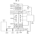
- FIG. 12 is a diagram showing an example of a scanning electron microscope that performs beam irradiation for precharging as described above and measurement of a pattern based on a signal waveform.
- An electron beam 1203 extracted from an electron source 1201 by an extraction electrode 1202 and accelerated by an acceleration electrode (not shown) is focused by a condenser lens 1204 which is a form of a focusing lens, and then is scanned on a sample 1209 by a scanning deflector 1205. Are scanned one-dimensionally or two-dimensionally.
- the electron beam 1203 is decelerated by a negative voltage applied to an electrode built in the sample stage 1208, and is focused by the lens action of the objective lens 1206 and irradiated onto the sample 1209.
- secondary electrons and electrons 1210 such as backscattered electrons are emitted from the irradiated portion.
- the emitted electrons 1210 are accelerated in the direction of the electron source by the acceleration action based on the negative voltage applied to the sample, and collide with the conversion electrode 1212 to generate secondary electrons 1211.
- the secondary electrons 1211 emitted from the conversion electrode 1212 are captured by the detector 1213, and the output of the detector 1213 changes depending on the amount of captured secondary electrons. In accordance with this output, the brightness of a display device (not shown) changes.
- an image of the scanning region is formed by synchronizing the deflection signal to the scanning deflector 1205 and the output of the detector 1213.
- the scanning deflector 1205 may be supplied with a deflection signal for moving the field of view in addition to a deflection signal for performing two-dimensional scanning within the field of view.
- This deflection by the deflection signal is also called image shift deflection, and enables movement of the field of view of the electron microscope without moving the sample by the sample stage.
- image shift deflection and scanning deflection are performed by a common deflector is shown, but an image shift deflector and a scanning deflector may be provided separately.
- an energy filter 1218 for energy discrimination of electrons emitted from the sample is installed between the sample 1209 and the conversion electrode 1212.
- the energy filter is composed of, for example, three mesh electrodes, and forms an electric field that reflects electrons from the sample 1209 toward the conversion electrode 1212. By adjusting the voltage applied to the mesh electrode, the energy of electrons that can pass through can be adjusted.
- FIG. 12 demonstrates the example which detects the electron emitted from the sample by converting once with a conversion electrode, of course, it is not restricted to such a structure, for example, it is It is possible to adopt a configuration in which the detection surface of the electron multiplier tube or the detector is arranged on the orbit.
- the control device 1220 controls each component of the scanning electron microscope, and forms a pattern on the sample based on the function of forming an image based on the detected electrons and the intensity distribution of detected electrons called a line profile. It has a function to measure the pattern width.
- the scanning electron microscope illustrated in FIG. 12 is provided with a pre-exhaust chamber 1215 for pre-exhausting the sample atmosphere when a sample is introduced into the sample chamber 1207 and a mini-en 1217 for forming an air cleaning space. Further, vacuum valves 1214 and 1216 for performing vacuum sealing are provided between these spaces.
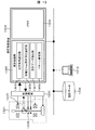
- FIG. 13 is a detailed explanatory diagram of a measurement or inspection system including an SEM.
- This system includes a scanning electron microscope system including an SEM main body 1301, a control device 1220 of the SEM main body, and an arithmetic processing device 1302.
- the arithmetic processing unit 1302 supplies a predetermined control signal to the control unit 1220 and executes signal processing of the signal obtained by the SEM main body 1301 and the obtained image information and recipe information.
- a memory 1304 for storing is incorporated.
- the control device 1220 and the arithmetic processing device 1302 are described as separate units, but may be an integrated control device.
- Electrons emitted from the sample or generated at the conversion electrode are captured by the detector 1213 and converted into a digital signal by an A / D converter built in the control device 1220.
- Image processing according to the purpose is performed by image processing hardware such as a CPU, ASIC, and FPGA incorporated in the arithmetic processing unit 1302.
- the arithmetic processing unit 1303 includes an optical condition setting unit 1305 for setting the optical conditions of the SEM based on the measurement conditions input by the input device 1310, and charged beam irradiation for selecting a charged beam irradiation region (or position) to be described later.
- a site selection unit 1306 is incorporated.
- the arithmetic processing unit 1303 includes a design data extraction unit 1307 that reads design data from the design data storage medium 1309 according to conditions input by the input device 1310 and converts the vector data into layout data as necessary. Has been.
- a pattern measuring unit 1308 for measuring the dimension of the pattern based on the acquired signal waveform is incorporated.
- the pattern measurement unit 1308 forms a line profile based on, for example, the detection signal, and performs dimension measurement between the peaks of the profile.
- the beam irradiation position or the scanning position is changed by controlling the drive signal of the sample stage 1208 or the supply signal to the deflector 1205.
- a GUI for displaying images, inspection results, and the like is displayed to the operator.
- the input device 1310 is an imaging recipe creation device that sets measurement conditions including the coordinates of the electronic device, the type of pattern, and imaging conditions (optical conditions and stage movement conditions) required for inspection and the like as imaging recipes. Also works.
- the input device 1310 also has a function of collating the input coordinate information and information on the pattern type with the layer information of the design data and the pattern identification information, and reading out necessary information from the design data storage medium 1309. Yes.
- Design data stored in the design data storage medium 1309 is expressed in the GDS format, OASIS format, etc., and is stored in a predetermined format.
- the design data can be of any type as long as the software that displays the design data can display the format and handle it as graphic data.
- the graphic data is a line segment that has been subjected to a deformation process that approximates the actual pattern by performing an exposure simulation instead of the line segment image information indicating the ideal shape of the pattern formed based on the design data. It may be image information.
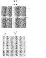
- FIG. 1 is a view showing a top view (Side View) and a side view (Side View) of a deep groove pattern composed of five kinds of materials.
- material A is a conductor
- materials B, C and E are insulators
- material D is a conductor (floating electrode).
- the sample is positioned below the measurement target pattern in order to clarify the contrast.
- An example of irradiating a pre-charging beam to a position different from the measurement target pattern by moving the field of view (Field of View: FOV) so that the lower layer pattern irradiates other patterns located in the lower layer. Will be explained.
- FOV Field of View
- FIG. 3 is a flowchart showing an SEM observation process including a preliminary charging beam irradiation process.
- a place to perform local preliminary irradiation a place where the observation place and the groove bottom are connected is selected (step 9).
- local preliminary irradiation conditions and observation conditions are set (step 10).
- FIG. 4 shows the charge distribution in the groove during local preliminary irradiation and observation.
- the negative charging of the groove side wall forms a barrier potential (returned back toward the groove bottom) to the secondary electrons generated at the groove bottom.
- the effect of the local preliminary irradiation is reduced. Disappear. For this reason, it is necessary to perform local preliminary irradiation and observation in another place where the material D of the groove bottom is connected.
- the material D that is a floating electrode is negatively charged (step 11).
- an electric field is formed in the groove at the observation place from the surface toward the groove bottom.
- it moves to the observation place where the material D was connected step 12
- observation is carried out at a preset magnification (step 13).
- the secondary electrons emitted from the groove bottom are pulled up by the electric field formed by the negative charge at the groove bottom, and the contrast of the groove bottom increases.
- the bottom of the groove is negatively charged with respect to the surface, and the number of secondary electrons detected from the groove bottom is increased.
- the method for specifying the location for local preliminary irradiation will be described.
- the irradiation location is determined by superimposing the layout pattern on the lower layer of the device and the observation image acquired at a low magnification.
- FIG. 5 shows an example in which the observation image acquired at a low magnification and the layout pattern of the lower layer of the device are superimposed on the line & space and hole pattern.
- Specified pre-irradiation location is arbitrarily set by the operator using the cursor box.
- an irradiation range, irradiation time, and irradiation current amount are designated.
- the relationship between the irradiation current amount and the charge accumulation amount (negative charging potential) is obtained in advance, by specifying the necessary potential, either the irradiation time or the irradiation current amount is automatically determined as a parameter. .
- observation location Specified observation location, observation magnification, irradiation current amount, and number of frames as observation condition settings.
- the observation location is designated on the GUI screen using a cursor box, as in the preliminary irradiation.
- the region of the material D that is the lower layer pattern is wide, as shown in FIG. 6, it is possible to observe a plurality of locations by one local preliminary irradiation, and it is possible to reduce the frequency of the local preliminary irradiation. . It is also possible for the operator to specify the frequency of local preliminary irradiation and observation in combination.
- These setting contents are stored as a recipe on the internal memory or the hard disk, and can be reused in another measurement. After the conditions are set, preliminary irradiation and observation are automatically performed by executing the recipe.
- the emphasis of the pattern bottom signal according to the present embodiment can be applied not only to the deep groove but also to a deep hole or a via shape as long as the bottom of the pattern is a floating electrode.
- FIG. 14 is a diagram showing an example of a GUI screen for setting observation conditions (acquisition conditions for measurement images) and preliminary charging conditions on layout data created based on design data.
- This GUI screen is displayed on the display screen of the input device 1310, for example.
- the GUI screen illustrated in FIG. 14 is provided with a display area 1401 for displaying layout data and a setting window for setting beam irradiation conditions.
- the setting window is provided with a window for setting a beam condition for observation and a window for setting a beam condition for charging formation. Note that other windows may be provided so that other parameters can be set as necessary.
- a position information setting window for setting a measurement or a visual field position
- a setting window for setting a pattern type
- a beam acceleration voltage There are a setting window (Vacc: Acceleration Voltage), number of frames integrated (Number of Frames), size of field of view (FOV), and beam current (Probe Current).
- the layout data displayed in the display area 1401 may be read from the design data storage medium 1309 based on, for example, the setting of the measurement position or the visual field position.
- partial design data is read according to the coordinate information of the measurement position and visual field position and the size of the visual field to be set, and the part is converted into layout data and displayed on the display screen.
- the design data since the design data stores pattern and layer identification information, the design data may be read based on selection of pattern and layer identification information, coordinate information, and the like.
- layout data corresponding to the designated area is read and displayed on the display device.
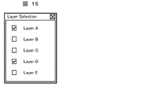
- a layer displayed in the display area 1401 may be selected using a layer selection window as illustrated in FIG.
- identification information is added to each layer, a desired layer can be selectively displayed by referring to the identification information.
- the charge forming beam condition setting window 1402 is a window for determining the type of beam irradiation condition.
- pre-irradiation is not performed (off)
- pre-irradiation is performed in a state where the observation visual field and the pre-charging visual field coincide with each other (On-Site)
- the observation visual field and the pre-charging visual field are used. It is possible to perform a setting such as performing pre-irradiation (Off-Site) with a distance between them.
- pre-irradiation area Pre-Dose FOV
- Pre-Dose time pre-irradiation time
- distance distance between the observation area 1403 and the pre-charged beam irradiation area 1404.
- Windows are provided.
- the pre-charged beam irradiation region 1404 has a predetermined size.
- the present invention is not limited to this, and a spot-shaped beam may be selectively irradiated to deep holes or deep grooves. good.
- FIG. 16 is a flowchart showing a process of automatically determining the irradiation region or irradiation position of the preliminary charging beam based on the selection of the type and location (position information such as coordinates) of the pattern to be measured.
- the type and location of the pattern to be measured are selected (step 1601).
- the design data extraction unit 1307 reads design data from the design data storage medium 1309 based on the pattern type and location information selected based on the selection, and generates layout data (step 1602). As described above, since identification information is added to the pattern and layer of the design data, the layout data of the pattern belonging to the desired pattern or region is read by referring to the information.
- a desired measurement site and image acquisition area are selected on the GUI screen (step 1603).
- the charged beam irradiation site selection unit 1306 selects a charging beam irradiation site or the like according to the selected measurement site or image acquisition region (step 1604).
- a pattern suitable as a charging beam irradiation target is (A) another pattern (upper layer pattern) in which the measurement target pattern and the lower layer wiring (floating electrode) are the same, and (B) a beam irradiation region for observation. It is a pattern that exists in an area that does not overlap. With respect to the condition (A), by referring to the design data, the overlapping part of the upper layer pattern and the lower layer pattern can be specified.
- the charging is automatically performed based on the calculation in the calculation processing unit 1303. It is possible to select the irradiation site of the beam for use. When a plurality of charging beam irradiation site candidates are extracted or there are no candidates, a manual assisted selection may be made by generating a message or an error message that prompts further narrowing down. good. Further, not only the conditions (A) and (B), but narrowing using other conditions may be performed automatically.
- the automatically selected charging beam irradiation conditions are registered as a recipe, for example, in the memory 1304 (step 1605).
- the second embodiment When observing a sample having a high aspect ratio, the contrast between the surface and the pattern bottom is excessive, and it may be difficult to observe the pattern bottom.
- a method for emphasizing the signal at the bottom of the pattern by using images acquired under different conditions in such a case will be described.
- the signal of the hole bottom is enhanced by combining the image observed under the condition where the local preliminary irradiation is not performed and the image observed after the local preliminary irradiation is performed on the groove bottom.
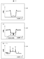
- FIG. 7 shows a signal waveform (1) when observed without performing local preliminary irradiation and a signal waveform observed after local preliminary irradiation. Since the charged state of the surface does not change, the signal waveform on the surface does not change.
- the signal waveform in the groove increases in signal amount in (2) because the material D is negatively charged by preliminary irradiation.
- the signal waveform observed without preliminary irradiation from the signal waveform at the time of observation after preliminary irradiation, it is possible to leave a signal of only the groove bottom, and it is possible to emphasize the signal in the groove.
- FIG. 17 is a diagram showing an example of a flowchart for automatically executing the measurement as described above.
- beam irradiation is performed on the measurement target pattern, and the first signal waveform 22 is acquired (steps 1701 and 1702).
- the beam irradiation position on the sample is moved by image shift or stage movement, and the charging beam is irradiated (step 1703).
- the beam is again irradiated to the measurement target pattern, and the second signal waveform 23 is acquired (steps 1704 and 1705).
- the pattern measuring unit 1308 calculates a difference between the first signal waveform 22 and the second signal waveform 23 (second signal waveform-first signal waveform), and uses the obtained difference profile 24 to measure the dimension. Are executed (steps 1706 and 1707).
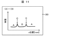
- this difference calculation has not only the effect of losing the luminance information of the material A but also the effect of clarifying the contrast between the material C and the material D.
- the material D is selectively charged, so that the luminance of the material D is greatly improved.
- the detection efficiency of the electrons emitted from the material C is slightly improved due to the influence of the charging of the material D, the improvement in the detection efficiency is relatively limited because the material C itself is not charged. Yes. Therefore, the selective charging of the material D can increase the contrast between the material C and the material D, and the peak of the material C can be made to stand out by the difference calculation. Thus, by revealing the peak of the material C, for example, the quality of the material C can be properly evaluated.
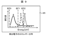
- FIG. 8 shows the energy distribution of electrons detected from each location when the structure shown in FIG.
- the signal waveform 25 (FIG. 8A) is a signal waveform when there is no preliminary irradiation
- the signal waveform 26 (FIG. 8B) is a signal waveform when there is preliminary irradiation.
- the energy distribution of detected electrons from the groove bottom is different from the distribution of detected electrons from the surface because the groove bottom is negatively charged. For this reason, when observing after preliminary irradiation, the signal at the groove bottom can be emphasized by discriminating the detected electrons based on energy.
- FIG. 9 shows a signal waveform 26 of electron energy distribution obtained by electron beam scanning after preliminary irradiation.
- energy distribution information including three peaks can be obtained.
- EF1-EF2 electrons in the energy band
- a signal waveform or image in which the contrast of the material C is enhanced can be formed.
- the material C A signal waveform and an image with enhanced contrast can be formed.
- the energy filter is a high-pass filter that cuts electrons having low energy, and energy of passing electrons can be selected by appropriately selecting an applied voltage.
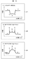
- FIG. 10 is a diagram showing the types of waveform signals obtained by adjusting the voltage applied to the energy filter 1218.
- the signal waveform 27 in FIG. 10A is a waveform in which the hole bottom is dark because the signal amount of the material A having a large number of detections is large and the signal amount of the hole bottom is small.
- the voltage applied to the energy filter is set to EF1
- electrons emitted from the material A having no negative charge and relatively low energy are restricted from passing through the energy filter 1218.
- the signal amounts of the materials C and D are relatively increased, and a signal waveform or an image having a bright hole bottom can be formed.
- the voltage applied to the energy filter is set to EF2
- the electrons emitted from the materials A and C are restricted from passing through the energy filter 1218, and therefore the material D as shown in the signal waveform 29 of FIG. A signal waveform and an image in which the above signal is emphasized can be obtained.
- FIG. 18 is a flowchart illustrating a process of performing measurement using a signal waveform in which the signal of the material C as exemplified in FIG. 11 is emphasized.
- a charged beam is irradiated to a charged beam irradiation portion (step 1801).
- the control device 1220 sets the voltage applied to the energy filter 1218 to Condition 1 (EF1), and irradiates the measurement target pattern with a beam to acquire a first signal waveform (Steps 1802 and 1803).
- the voltage applied to the energy filter is set to condition 2 (EF2), and the second signal waveform is acquired by irradiating the measurement target pattern with a beam (steps 1804 and 1805).
- EF1 Condition 1
- EF2 condition 2
- the pattern measuring unit 1308 calculates a difference between the first signal waveform 28 and the second signal waveform 29 (second signal waveform-first signal waveform), and uses the obtained difference profile 30 to measure the dimension. Are executed (steps 1806 and 1807).
- FIG. 19 is a diagram showing an apparatus configuration for detecting electrons of different energy bands using detectors 1907 and 1908 provided at different positions. Electrons 1902 emitted from the sample 1901 are deflected toward the detector so as to deviate from the ideal optical axis 1904 of the electron beam by the deflection action of the orthogonal electromagnetic field generator 1903.
- the orthogonal electromagnetic field generator 1903 is provided with a magnetic field generator so that a magnetic field is formed so as to be orthogonal to an electric field that deflects the electrons 1902 toward the detector.
- This magnetic field acts on the electrons 1902 so as to guide the electrons 1902 to the detector side.
- the electron beam irradiated to the sample is deflected in the direction opposite to the deflecting action of the electric field. The electrons emitted from the sample can be selectively guided to the detector side without deflecting.
- the orthogonal electromagnetic field generator 1903 deflects electrons having low energy more greatly, the electrons in the first energy band (EF1-EF2) are detected using the lower detector 1908, and the second energy band is detected.
- Energy discrimination detection can be performed by adjusting the orthogonal electromagnetic field generator 1903 so that ( ⁇ EF2) electrons are detected using the upper detector 1907.
- a signal in which the luminance of a desired material is selectively enhanced can be formed by combining the outputs of the two detectors after setting the amplification factor of the amplifier 1809 appropriately.
Landscapes
- Physics & Mathematics (AREA)
- Electromagnetism (AREA)
- General Physics & Mathematics (AREA)
- Chemical & Material Sciences (AREA)
- Analytical Chemistry (AREA)
- Testing Or Measuring Of Semiconductors Or The Like (AREA)
- Length-Measuring Devices Using Wave Or Particle Radiation (AREA)
Priority Applications (2)
| Application Number | Priority Date | Filing Date | Title |
|---|---|---|---|
| KR1020147018326A KR101622613B1 (ko) | 2012-03-28 | 2013-02-18 | 주사 전자 현미경 |
| US14/379,715 US9472376B2 (en) | 2012-03-28 | 2013-02-18 | Scanning electron microscope |
Applications Claiming Priority (2)
| Application Number | Priority Date | Filing Date | Title |
|---|---|---|---|
| JP2012-072710 | 2012-03-28 | ||
| JP2012072710A JP5932428B2 (ja) | 2012-03-28 | 2012-03-28 | 走査電子顕微鏡 |
Publications (1)
| Publication Number | Publication Date |
|---|---|
| WO2013145924A1 true WO2013145924A1 (ja) | 2013-10-03 |
Family
ID=49259206
Family Applications (1)
| Application Number | Title | Priority Date | Filing Date |
|---|---|---|---|
| PCT/JP2013/053790 Ceased WO2013145924A1 (ja) | 2012-03-28 | 2013-02-18 | 走査電子顕微鏡 |
Country Status (4)
| Country | Link |
|---|---|
| US (1) | US9472376B2 (enExample) |
| JP (1) | JP5932428B2 (enExample) |
| KR (1) | KR101622613B1 (enExample) |
| WO (1) | WO2013145924A1 (enExample) |
Families Citing this family (7)
| Publication number | Priority date | Publication date | Assignee | Title |
|---|---|---|---|---|
| US9330884B1 (en) * | 2014-11-11 | 2016-05-03 | ICT Integrated Circuit Testing Gesellschaft für Halbleiterprüftechnik mbH | Dome detection for charged particle beam device |
| JP2019185972A (ja) | 2018-04-06 | 2019-10-24 | 株式会社日立ハイテクノロジーズ | 走査電子顕微鏡システム及びパターンの深さ計測方法 |
| JP2019184354A (ja) * | 2018-04-06 | 2019-10-24 | 株式会社日立ハイテクノロジーズ | 電子顕微鏡装置、電子顕微鏡装置を用いた検査システム及び電子顕微鏡装置を用いた検査方法 |
| JP7150634B2 (ja) * | 2019-02-21 | 2022-10-11 | 株式会社荏原製作所 | 電子線照射装置および電子ビームの位置合わせ方法 |
| JP2021005497A (ja) * | 2019-06-26 | 2021-01-14 | キオクシア株式会社 | 電子顕微鏡およびビーム照射方法 |
| JP7149906B2 (ja) | 2019-08-07 | 2022-10-07 | 株式会社日立ハイテク | 走査電子顕微鏡及びパタン計測方法 |
| JP7218034B1 (ja) * | 2022-11-04 | 2023-02-06 | 株式会社Photo electron Soul | 局所観察方法、プログラム、記録媒体および電子線適用装置 |
Citations (2)
| Publication number | Priority date | Publication date | Assignee | Title |
|---|---|---|---|---|
| JPH01115042A (ja) * | 1987-10-28 | 1989-05-08 | Hitachi Ltd | 走査型電子顕微鏡の試料台 |
| JPH05259240A (ja) * | 1992-03-11 | 1993-10-08 | Matsushita Electron Corp | 半導体装置の評価方法 |
Family Cites Families (12)
| Publication number | Priority date | Publication date | Assignee | Title |
|---|---|---|---|---|
| US4327292A (en) * | 1980-05-13 | 1982-04-27 | Hughes Aircraft Company | Alignment process using serial detection of repetitively patterned alignment marks |
| JP2650930B2 (ja) * | 1987-11-24 | 1997-09-10 | 株式会社日立製作所 | 超格子構作の素子製作方法 |
| JPH0529424A (ja) | 1991-07-19 | 1993-02-05 | Fujitsu Ltd | 半導体装置の検査方法 |
| DE69231213T2 (de) * | 1991-11-27 | 2001-03-01 | Hitachi Science Systems Ltd., Hitachinaka | Elektronenstrahlgerät |
| JP3749107B2 (ja) * | 1999-11-05 | 2006-02-22 | ファブソリューション株式会社 | 半導体デバイス検査装置 |
| JP4418304B2 (ja) | 2004-06-03 | 2010-02-17 | 株式会社日立ハイテクノロジーズ | 試料観察方法 |
| JP2008004376A (ja) | 2006-06-22 | 2008-01-10 | Seiko Epson Corp | デバイス、薄膜形成方法及びデバイスの製造方法並びに電子機器 |
| JP5028159B2 (ja) * | 2007-06-29 | 2012-09-19 | 株式会社日立ハイテクノロジーズ | 荷電粒子線装置 |
| TWI585806B (zh) * | 2008-04-11 | 2017-06-01 | 荏原製作所股份有限公司 | 試料觀察方法與裝置,及使用該方法與裝置之檢查方法與裝置 |
| JP2010118414A (ja) | 2008-11-11 | 2010-05-27 | Topcon Corp | 半導体検査装置 |
| JP2010175249A (ja) | 2009-01-27 | 2010-08-12 | Hitachi High-Technologies Corp | 試料高さ測定方法及び試料高さ測定装置 |
| JP5537288B2 (ja) * | 2010-06-30 | 2014-07-02 | 株式会社日立ハイテクノロジーズ | 電子ビームの照射方法及び走査電子顕微鏡 |
-
2012
- 2012-03-28 JP JP2012072710A patent/JP5932428B2/ja active Active
-
2013
- 2013-02-18 US US14/379,715 patent/US9472376B2/en active Active
- 2013-02-18 WO PCT/JP2013/053790 patent/WO2013145924A1/ja not_active Ceased
- 2013-02-18 KR KR1020147018326A patent/KR101622613B1/ko active Active
Patent Citations (2)
| Publication number | Priority date | Publication date | Assignee | Title |
|---|---|---|---|---|
| JPH01115042A (ja) * | 1987-10-28 | 1989-05-08 | Hitachi Ltd | 走査型電子顕微鏡の試料台 |
| JPH05259240A (ja) * | 1992-03-11 | 1993-10-08 | Matsushita Electron Corp | 半導体装置の評価方法 |
Also Published As
| Publication number | Publication date |
|---|---|
| JP2013206641A (ja) | 2013-10-07 |
| US20150008322A1 (en) | 2015-01-08 |
| KR20140109920A (ko) | 2014-09-16 |
| US9472376B2 (en) | 2016-10-18 |
| JP5932428B2 (ja) | 2016-06-08 |
| KR101622613B1 (ko) | 2016-05-20 |
Similar Documents
| Publication | Publication Date | Title |
|---|---|---|
| JP5932428B2 (ja) | 走査電子顕微鏡 | |
| JP6316578B2 (ja) | 走査電子顕微鏡システム及びそれを用いたパターン計測方法並びに走査電子顕微鏡 | |
| JP5948084B2 (ja) | 走査電子顕微鏡 | |
| JP6255448B2 (ja) | 荷電粒子線装置の装置条件設定方法、および荷電粒子線装置 | |
| US10984981B2 (en) | Charged particle beam device having inspection scan direction based on scan with smaller dose | |
| JP6216515B2 (ja) | 電子ビーム装置、及び電子ビーム観察方法 | |
| US8969801B2 (en) | Scanning electron microscope | |
| JP6267529B2 (ja) | 荷電粒子線装置及び画像生成方法 | |
| US9536700B2 (en) | Sample observation device | |
| JP2010175249A (ja) | 試料高さ測定方法及び試料高さ測定装置 | |
| US11211226B2 (en) | Pattern cross-sectional shape estimation system and program | |
| JPWO2017179138A1 (ja) | パターン計測装置およびパターン計測方法 | |
| US10879037B2 (en) | Charged particle beam device with distance setting between irradiation regions in a scan line | |
| US20070187599A1 (en) | Charged particle beam apparatus, charged particle beam focusing method, microstructure measuring method, microstructure inspecting method, semiconductor device manufacturing method, and program | |
| JP5222994B2 (ja) | 試料観察方法および走査電子顕微鏡 | |
| JP5619118B2 (ja) | 荷電粒子線装置 | |
| JP2005061998A (ja) | 表面電位測定方法及び試料観察方法 | |
| JP2006172919A (ja) | 三次元形状解析機能を有する走査型電子顕微鏡 | |
| WO2013011792A1 (ja) | 試料の検査条件・測定条件の自動判定方法及び走査型顕微鏡 | |
| JP2016139531A (ja) | 試料の観察、検査、測定方法、及び走査電子顕微鏡 | |
| JP2009224289A (ja) | 荷電粒子ビーム装置 |
Legal Events
| Date | Code | Title | Description |
|---|---|---|---|
| 121 | Ep: the epo has been informed by wipo that ep was designated in this application |
Ref document number: 13767610 Country of ref document: EP Kind code of ref document: A1 |
|
| ENP | Entry into the national phase |
Ref document number: 20147018326 Country of ref document: KR Kind code of ref document: A |
|
| WWE | Wipo information: entry into national phase |
Ref document number: 14379715 Country of ref document: US |
|
| NENP | Non-entry into the national phase |
Ref country code: DE |
|
| 122 | Ep: pct application non-entry in european phase |
Ref document number: 13767610 Country of ref document: EP Kind code of ref document: A1 |