WO2013136809A1 - 画像処理装置、撮像装置および画像処理プログラム - Google Patents
画像処理装置、撮像装置および画像処理プログラム Download PDFInfo
- Publication number
- WO2013136809A1 WO2013136809A1 PCT/JP2013/001746 JP2013001746W WO2013136809A1 WO 2013136809 A1 WO2013136809 A1 WO 2013136809A1 JP 2013001746 W JP2013001746 W JP 2013001746W WO 2013136809 A1 WO2013136809 A1 WO 2013136809A1
- Authority
- WO
- WIPO (PCT)
- Prior art keywords
- pixel
- parallax
- color
- image
- pixel value
- Prior art date
Links
- 238000012545 processing Methods 0.000 title claims abstract description 92
- 238000003384 imaging method Methods 0.000 title claims description 41
- 238000012935 Averaging Methods 0.000 claims abstract description 22
- 238000000034 method Methods 0.000 claims description 107
- 238000009826 distribution Methods 0.000 claims description 68
- 238000004364 calculation method Methods 0.000 claims description 39
- 230000008569 process Effects 0.000 claims description 29
- 230000003287 optical effect Effects 0.000 claims description 18
- 238000003672 processing method Methods 0.000 claims 12
- 239000003086 colorant Substances 0.000 abstract description 13
- 238000006243 chemical reaction Methods 0.000 description 80
- 238000012937 correction Methods 0.000 description 44
- 230000004907 flux Effects 0.000 description 35
- 238000010586 diagram Methods 0.000 description 29
- 230000003252 repetitive effect Effects 0.000 description 27
- 210000001747 pupil Anatomy 0.000 description 15
- 230000004304 visual acuity Effects 0.000 description 11
- 238000005516 engineering process Methods 0.000 description 10
- 230000006870 function Effects 0.000 description 9
- 230000008859 change Effects 0.000 description 8
- 230000007423 decrease Effects 0.000 description 8
- 230000000694 effects Effects 0.000 description 8
- 238000006073 displacement reaction Methods 0.000 description 5
- 230000002093 peripheral effect Effects 0.000 description 5
- 238000013213 extrapolation Methods 0.000 description 4
- 238000005286 illumination Methods 0.000 description 4
- 230000008033 biological extinction Effects 0.000 description 3
- 230000006872 improvement Effects 0.000 description 3
- 238000004519 manufacturing process Methods 0.000 description 3
- 230000003044 adaptive effect Effects 0.000 description 2
- 230000000903 blocking effect Effects 0.000 description 2
- 230000000295 complement effect Effects 0.000 description 2
- 238000001514 detection method Methods 0.000 description 2
- 239000000284 extract Substances 0.000 description 2
- 238000000605 extraction Methods 0.000 description 2
- 230000035945 sensitivity Effects 0.000 description 2
- 239000000758 substrate Substances 0.000 description 2
- 230000007704 transition Effects 0.000 description 2
- 229910004298 SiO 2 Inorganic materials 0.000 description 1
- 230000009471 action Effects 0.000 description 1
- 230000002411 adverse Effects 0.000 description 1
- 238000013459 approach Methods 0.000 description 1
- 230000008901 benefit Effects 0.000 description 1
- 239000002131 composite material Substances 0.000 description 1
- 230000008034 disappearance Effects 0.000 description 1
- 238000005530 etching Methods 0.000 description 1
- 238000002474 experimental method Methods 0.000 description 1
- 230000004438 eyesight Effects 0.000 description 1
- 238000010030 laminating Methods 0.000 description 1
- 239000011159 matrix material Substances 0.000 description 1
- 238000012986 modification Methods 0.000 description 1
- 230000004048 modification Effects 0.000 description 1
- 230000000737 periodic effect Effects 0.000 description 1
- 238000005070 sampling Methods 0.000 description 1
- 238000000926 separation method Methods 0.000 description 1
- 230000003595 spectral effect Effects 0.000 description 1
Images


Classifications
-
- H—ELECTRICITY
- H04—ELECTRIC COMMUNICATION TECHNIQUE
- H04N—PICTORIAL COMMUNICATION, e.g. TELEVISION
- H04N13/00—Stereoscopic video systems; Multi-view video systems; Details thereof
- H04N13/20—Image signal generators
- H04N13/204—Image signal generators using stereoscopic image cameras
- H04N13/207—Image signal generators using stereoscopic image cameras using a single 2D image sensor
- H04N13/218—Image signal generators using stereoscopic image cameras using a single 2D image sensor using spatial multiplexing
-
- H—ELECTRICITY
- H04—ELECTRIC COMMUNICATION TECHNIQUE
- H04N—PICTORIAL COMMUNICATION, e.g. TELEVISION
- H04N13/00—Stereoscopic video systems; Multi-view video systems; Details thereof
- H04N13/10—Processing, recording or transmission of stereoscopic or multi-view image signals
- H04N13/106—Processing image signals
- H04N13/111—Transformation of image signals corresponding to virtual viewpoints, e.g. spatial image interpolation
-
- H—ELECTRICITY
- H01—ELECTRIC ELEMENTS
- H01L—SEMICONDUCTOR DEVICES NOT COVERED BY CLASS H10
- H01L27/00—Devices consisting of a plurality of semiconductor or other solid-state components formed in or on a common substrate
- H01L27/14—Devices consisting of a plurality of semiconductor or other solid-state components formed in or on a common substrate including semiconductor components sensitive to infrared radiation, light, electromagnetic radiation of shorter wavelength or corpuscular radiation and specially adapted either for the conversion of the energy of such radiation into electrical energy or for the control of electrical energy by such radiation
- H01L27/144—Devices controlled by radiation
- H01L27/146—Imager structures
- H01L27/14601—Structural or functional details thereof
- H01L27/1462—Coatings
- H01L27/14621—Colour filter arrangements
-
- H—ELECTRICITY
- H01—ELECTRIC ELEMENTS
- H01L—SEMICONDUCTOR DEVICES NOT COVERED BY CLASS H10
- H01L27/00—Devices consisting of a plurality of semiconductor or other solid-state components formed in or on a common substrate
- H01L27/14—Devices consisting of a plurality of semiconductor or other solid-state components formed in or on a common substrate including semiconductor components sensitive to infrared radiation, light, electromagnetic radiation of shorter wavelength or corpuscular radiation and specially adapted either for the conversion of the energy of such radiation into electrical energy or for the control of electrical energy by such radiation
- H01L27/144—Devices controlled by radiation
- H01L27/146—Imager structures
- H01L27/14601—Structural or functional details thereof
- H01L27/14625—Optical elements or arrangements associated with the device
- H01L27/14627—Microlenses
-
- H—ELECTRICITY
- H01—ELECTRIC ELEMENTS
- H01L—SEMICONDUCTOR DEVICES NOT COVERED BY CLASS H10
- H01L27/00—Devices consisting of a plurality of semiconductor or other solid-state components formed in or on a common substrate
- H01L27/14—Devices consisting of a plurality of semiconductor or other solid-state components formed in or on a common substrate including semiconductor components sensitive to infrared radiation, light, electromagnetic radiation of shorter wavelength or corpuscular radiation and specially adapted either for the conversion of the energy of such radiation into electrical energy or for the control of electrical energy by such radiation
- H01L27/144—Devices controlled by radiation
- H01L27/146—Imager structures
- H01L27/14643—Photodiode arrays; MOS imagers
- H01L27/14645—Colour imagers
-
- H—ELECTRICITY
- H04—ELECTRIC COMMUNICATION TECHNIQUE
- H04N—PICTORIAL COMMUNICATION, e.g. TELEVISION
- H04N13/00—Stereoscopic video systems; Multi-view video systems; Details thereof
- H04N13/10—Processing, recording or transmission of stereoscopic or multi-view image signals
- H04N13/106—Processing image signals
- H04N13/15—Processing image signals for colour aspects of image signals
-
- H—ELECTRICITY
- H04—ELECTRIC COMMUNICATION TECHNIQUE
- H04N—PICTORIAL COMMUNICATION, e.g. TELEVISION
- H04N13/00—Stereoscopic video systems; Multi-view video systems; Details thereof
- H04N13/20—Image signal generators
- H04N13/204—Image signal generators using stereoscopic image cameras
- H04N13/207—Image signal generators using stereoscopic image cameras using a single 2D image sensor
-
- H—ELECTRICITY
- H04—ELECTRIC COMMUNICATION TECHNIQUE
- H04N—PICTORIAL COMMUNICATION, e.g. TELEVISION
- H04N13/00—Stereoscopic video systems; Multi-view video systems; Details thereof
- H04N13/20—Image signal generators
- H04N13/257—Colour aspects
-
- H—ELECTRICITY
- H04—ELECTRIC COMMUNICATION TECHNIQUE
- H04N—PICTORIAL COMMUNICATION, e.g. TELEVISION
- H04N23/00—Cameras or camera modules comprising electronic image sensors; Control thereof
- H04N23/80—Camera processing pipelines; Components thereof
- H04N23/84—Camera processing pipelines; Components thereof for processing colour signals
- H04N23/843—Demosaicing, e.g. interpolating colour pixel values
-
- H—ELECTRICITY
- H04—ELECTRIC COMMUNICATION TECHNIQUE
- H04N—PICTORIAL COMMUNICATION, e.g. TELEVISION
- H04N25/00—Circuitry of solid-state image sensors [SSIS]; Control thereof
- H04N25/10—Circuitry of solid-state image sensors [SSIS]; Control thereof for transforming different wavelengths into image signals
- H04N25/11—Arrangement of colour filter arrays [CFA]; Filter mosaics
- H04N25/13—Arrangement of colour filter arrays [CFA]; Filter mosaics characterised by the spectral characteristics of the filter elements
- H04N25/134—Arrangement of colour filter arrays [CFA]; Filter mosaics characterised by the spectral characteristics of the filter elements based on three different wavelength filter elements
-
- H—ELECTRICITY
- H04—ELECTRIC COMMUNICATION TECHNIQUE
- H04N—PICTORIAL COMMUNICATION, e.g. TELEVISION
- H04N25/00—Circuitry of solid-state image sensors [SSIS]; Control thereof
- H04N25/70—SSIS architectures; Circuits associated therewith
- H04N25/703—SSIS architectures incorporating pixels for producing signals other than image signals
- H04N25/704—Pixels specially adapted for focusing, e.g. phase difference pixel sets
-
- H—ELECTRICITY
- H04—ELECTRIC COMMUNICATION TECHNIQUE
- H04N—PICTORIAL COMMUNICATION, e.g. TELEVISION
- H04N23/00—Cameras or camera modules comprising electronic image sensors; Control thereof
- H04N23/10—Cameras or camera modules comprising electronic image sensors; Control thereof for generating image signals from different wavelengths
-
- H—ELECTRICITY
- H04—ELECTRIC COMMUNICATION TECHNIQUE
- H04N—PICTORIAL COMMUNICATION, e.g. TELEVISION
- H04N23/00—Cameras or camera modules comprising electronic image sensors; Control thereof
- H04N23/60—Control of cameras or camera modules
- H04N23/67—Focus control based on electronic image sensor signals
- H04N23/672—Focus control based on electronic image sensor signals based on the phase difference signals
-
- H—ELECTRICITY
- H04—ELECTRIC COMMUNICATION TECHNIQUE
- H04N—PICTORIAL COMMUNICATION, e.g. TELEVISION
- H04N25/00—Circuitry of solid-state image sensors [SSIS]; Control thereof
- H04N25/70—SSIS architectures; Circuits associated therewith
- H04N25/702—SSIS architectures characterised by non-identical, non-equidistant or non-planar pixel layout
Definitions
- the present invention relates to an image processing device, an imaging device, and an image processing program.
- Patent Literature Japanese Patent Application Laid-Open No. 2003-7994
- an unbalance such as illuminance mismatch occurs between parallax images as a unique phenomenon that occurs when a parallax pixel is combined with a single optical system.
- the imbalance between the parallax images has an adverse effect.
- An image processing apparatus includes a first filter having a first filter of a first component color among a plurality of color components constituting a color of a subject image and a first pixel having a non-parallax opening corresponding to a reference direction.
- An acquisition unit that acquires first image data including a third pixel value of a third pixel having a parallax opening that generates parallax in a direction opposite to one direction, and the pixel position of the second pixel A fourth pixel value obtained by averaging the second pixel value at the pixel position and the virtual third pixel value calculated using the third pixel value of the surrounding third pixel, and the pixel position of the third pixel
- the third pixel value at the pixel position and the surrounding A calculation unit for calculating a fifth pixel value obtained by averaging the virtual second pixel value calculated using the second pixel value of the second pixel, a first pixel value, a fourth pixel value, and a fifth pixel value;
- An image generation unit configured to generate second
- An imaging device is an imaging device including an imaging device that captures a subject image and the above-described image processing device, and the first image data is generated based on an output of the imaging device.
- An image processing program includes a first filter of a first component color among a plurality of color components constituting a color of a subject image and a first pixel having an opening with no parallax corresponding to a reference direction.
- FIG. 6 is a diagram for explaining a blurred subject image. It is a figure which shows the pixel arrangement
- 1 is a diagram illustrating a configuration of a digital camera 10.
- FIG. 2 is a diagram illustrating a cross-sectional configuration of an image sensor 100.
- FIG. 2 is a schematic diagram illustrating a state in which a part of the image sensor 100 is enlarged.
- FIG. It is a conceptual diagram explaining the relationship between a parallax pixel and a to-be-photographed object. It is a conceptual diagram explaining the process which produces
- the digital camera according to the present embodiment which is a form of the image processing apparatus and the imaging apparatus, is configured to be able to generate images with a plurality of viewpoints for one scene by one shooting. Each image having a different viewpoint is called a parallax image.
- Patent Document 1 a single-plate type Bayer array type color solid-state imaging device has a parallax pixel having only a left aperture spread on half of the pixels and a parallax pixel having only a right aperture spread on the other half of the pixels.
- An imaging method capable of forming a stereoscopic image by one imaging with a single camera is disclosed.
- Patent Document 1 does not clearly describe a specific method for generating left-eye and right-eye color images from imaging data. What kind of sensor characteristics the imaging element of a half-opening parallax pixel has, There is a problem that there is no description about what kind of problems are encountered in order to obtain a resolving stereoscopic image and what must be dealt with.
- An object of the present invention is to provide a method for generating a high-resolution stereoscopic image based on the optical system and sensor characteristics.
- the present invention solves the problem of illuminance distribution mismatch that occurs between left-eye and right-eye pixels when a three-dimensional image is captured using a single-plate image sensor having left-eye and right-eye half-opening parallax pixels. Appropriately handled, high-resolution right-eye and left-eye images can be generated.
- the color filter array has a Bayer array structure, and one G pixel is provided with a left-opening parallax pixel, and the other G pixel is provided with a right-opening parallax pixel as an opening mask. Further, the R pixel and the B pixel are provided with pixels with no parallax of all openings.
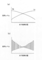
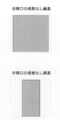
- the resolution related to the spatial frequency of this array is shown in Fig. 1 (bottom).
- the types of color filters and aperture masks are multiplexed on one sensor surface, when they are separated into specific colors of specific aperture masks and the critical resolution frequency is viewed, they are the Nyquist of the original pixel. It only has a resolution that never reaches the frequency.
- the final left-view color image is output to the original Nyquist frequency by superimposing the left-view image, which has only a small resolving power in the frequency space, and the intermediate image without parallax. can do.
- the color image of the right viewpoint is output to the original Nyquist frequency by superimposing the left-view image, which has only a small resolving power in the frequency space, and the intermediate image without parallax. can do.
- the color image of the right viewpoint is output to the original Nyquist frequency by superimposing the left-view image, which has only a small resolving power in the frequency space, and the intermediate image without parallax. can do.
- the color image of the right viewpoint is output to the original Nyquist frequency by superimposing the left-view image, which has only a small resolving power in the frequency space, and the intermediate image without parallax.
- the left parallax pixel is bright on the right side and dark on the left side of the image capturing the subject image.
- the right parallax pixel is brighter on the left side of the image and darker on the right side. That is, even if the subject image is the same, the right parallax pixel and the left parallax pixel are captured as images with completely different illuminance.
- a method for simultaneously solving the problem of illuminance mismatch between parallax pixels and the problem of subject position mismatch due to parallax based on the characteristics of the subject image of the monocular pupil division method. That is, as shown in FIG. 14, in the monocular pupil division imaging, the focused subject image does not cause a parallax shift in the left and right parallax pixels, and only the subject image at the out-of-focus position, A parallax shift occurs. That is, the parallax is included only in the blur. As shown in FIG. 3, the blurred subject image can generate an image without parallax by simply taking an average.
- the imaging signal is generated as it is without changing even if the parallax average between the left and right is taken, while at the position of the blurred subject image,
- the parallax average between the left and right disappears completely, and the problem of gain mismatch due to illuminance unevenness also disappears completely and can be solved simultaneously.
- arithmetic mean a subject image with a large blur width, which is the sum of the two blur widths, is generated at an intermediate position.
- geometric mean a subject image having the same blur width as the blur width divided into two is generated at the intermediate position.
- a subject image having the same blur width as that of the pixels with no parallax of the entire aperture is formed, and in the case of the geometric average, a subject image having the same blur width as that of the parallax pixels of the half aperture is formed.
- the intermediate image without parallax can be used as a conventional high-resolution two-dimensional image for monitor display and print output.
- a left parallax image and a right parallax image with low spatial frequency resolution are generated. Performs simple average interpolation in the G color plane, where only the left parallax pixels are collected. Linear interpolation is performed according to the ratio of distances using adjacent pixel values. Similarly, simple average interpolation in the G color plane in which only the right parallax pixels are collected is performed. That, Lt mosaic (x, y) Lt from (x, y) and, Rt mosaic (x, y) from the Rt (x, y) to produce a.
- Temporary left parallax image Lt (x, y)
- Temporary right parallax image Rt (x, y)
- step 4 Generation of parallax-free color mosaic image by correcting left and right illumination distribution (local gain balance correction)
- local gain correction is performed in units of pixels to match the illuminance of the left parallax pixel in the screen and the right parallax pixel in the screen.
- a new Bayer surface with gain matching is created. This is equivalent to replacing with an average value, and a Bayer surface in which the parallax disappears is created.
- M N x, y
- target value setting methods to be used as reference points for each pixel there are two types of target value setting methods to be used as reference points for each pixel: a method of selecting an arithmetic mean and a method of selecting a geometric mean.
- the process of applying local gain correction to each pixel is actually only necessary to substitute the average value of each pixel obtained first.
- the local gain correction is a modulation process for eliminating the parallax.
- an arithmetic average is employed. In this way, the Bayer plane data is rewritten using the average value of the left viewpoint image and the right viewpoint image as the non-parallax pixel value of the new G pixel position, and the Bayer plane image M N (x, y) without parallax is output. To do.
- the technology USP6,836,572 for increasing the resolution of the direction determination of the same inventor as the present applicant and resolving the vertical and horizontal Nyquist frequencies
- the technology USP7,236,628 for increasing the resolution in the oblique direction when calculating the interpolation value
- adaptive false color countermeasure technology USP7,391,903 by color gradient judgment method and technology to increase resolution of direction judgment The best high-performance demosaic technology used in is introduced.
- the positive offset value ⁇ is set to a larger value as the imaging condition with higher sensitivity increases the dark current noise component.
- step S4 the CPU performs an interpolation process as follows.
- a pixel having R component color information is referred to as an R pixel
- a pixel having B component color information is referred to as a B pixel
- a pixel having G component color information is referred to as a G pixel.
- the signal value of the R component corresponding to the pixel indicated by i, j] is R [i, j]
- the signal value of the G component is G [i, j]
- the signal value of the B component is B [i, j]. I will represent it.
- the CPU determines the vertical similarity CvN [i, j] and the horizontal similarity ChN [i, j] for the pixel (R pixel or B pixel) that is not the G pixel indicated by the pixel position [i, j].
- Z [i, j] is the signal value of the R component or B component indicated by the pixel position [i, j].
- the first term is the similarity between the same colors that represents the similarity between the same colors at two pixel intervals
- the second term is the similarity between the different colors that represents the similarity between the different colors at the adjacent pixel intervals.
- the similarity between different colors has the ability to resolve vertical and horizontal Nyquist frequencies.
- the absolute value of the first term in the above equations (3) and (4) is to detect rough directionality by comparing the G color components.
- the absolute values of the second and third terms in the above equations (3) and (4) detect fine similarities that cannot be detected by the first term.
- the CPU calculates the vertical similarity and the horizontal similarity obtained by the above formulas (3) and (4) for each coordinate, and calculates the vertical and horizontal similarity in the target coordinates [i, j]. Based on the following equation (5), the direction of similarity is determined.
- Th is a determination threshold value used to avoid erroneous determination due to noise included in the signal value, and is changed according to the ISO sensitivity.
- the CPU interpolates the G component using the unevenness information of the R component or the B component. That is, information on whether or not to interpolate to an external dividing point that cannot be predicted only by interpolation of the inner G component of the surrounding G component, information on the same color component that is located in the vicinity of information on other color components existing at the interpolation target position And determining whether the image structure is convex upward or downward. That is, the information of the high frequency component obtained by sampling other color components is superimposed on the interpolation target color component.
- the G color complement is calculated by the following formulas (6) and (9) when the vertical direction is similar to the position [i, j] of the center R pixel shown in FIG.
- Z [i, j] is the signal value of the R component or B component indicated by the pixel position [i, j].
- the first term in the above equation (9) is calculated from the G component signal values G [i, j-1] and G [i, j + 1] arranged vertically with respect to the pixel position [i, j]. Represents the average value.
- the second term in the above equation (9) is the amount of change calculated from the R component signal values R [i, j], R [i, j-2] and R [i, j + 2] arranged vertically. To express. By adding the amount of change in the R component signal value to the average value of the G component signal value, the G component interpolation value G [i, j] is obtained. Since such interpolation can be predicted except for the internal dividing point of the G component, it will be referred to as extrapolation for convenience.
- the above equation (10) performs extrapolation in the horizontal direction using the signal values of the pixels arranged horizontally with respect to the pixel position [i, j], as in the case of the extrapolation in the vertical direction described above. It is.
- the CPU calculates the G color interpolation values by the above formulas (9) and (10), and takes the average of the two calculated G color interpolation values. Let it be a G color interpolation value.
- R interpolation For R color interpolation, pixel positions [i + 1, j], [i, j + 1], [i + 1, j other than the R pixel position [i, j] shown in FIG. +1] is calculated by the following equations (11) to (13), respectively. At this time, unevenness information of G component signal values (FIG. 7 of WO2006 / 006373) corresponding to all pixel positions obtained by the G interpolation described above is used.
- the first term in the above equations (11) to (13) represents an average value calculated from the R component signal value adjacent to the coordinates to be subjected to R component interpolation, and the first term in the above equations (11) to (13).
- B interpolation For the B component interpolation, interpolation processing is performed in the same manner as the R component. For example, for pixel positions [i + 1, j], [i, j + 1], [i + 1, j + 1] other than the position [i, j] of the B pixel shown in FIG. 8 of WO2006 / 006373 Are calculated by the following equations (14) to (16), respectively. At this time, the unevenness information of the G component signal values (FIG. 9 of WO2006 / 006373) corresponding to all the pixel positions obtained by the G interpolation described above is used.
- the change amount of the G component signal value is added to the average value of the B component signal value to obtain the B component interpolation value.
- step 5-3 Transition to original linear gradation space by inverse gradation conversion
- the inverse gradation conversion of step 5-1 is performed on each Bayer-interpolated RGB color plane to return to linear gradation RGB data.
- the obtained RGB color image without parallax is represented by R N (x, y), G N (x, y), and B N (x, y). These are RGB data expressed in linear gradation.
- This can be called parallax modulation because the displacement processing is realized by superimposing the parallax components of the temporary parallax image.
- parallax modulation methods There are two types of parallax modulation methods: a method using an arithmetic average as a reference point and a method using a geometric average as a reference point. Both can obtain a parallax modulation effect, but when the aperture mask of pixels without parallax of the image sensor is full aperture, a method using an arithmetic average as a reference point is adopted, and the aperture mask of pixels without parallax is a pixel with parallax. It is better to adopt a method using the geometric mean as a reference point when the same half aperture is used. Therefore, in this embodiment, a method using an arithmetic mean as a reference point is used.
- step 6 the parallax modulation calculation formula defined in step 6 and the parallax extinction calculation formula (local gain balance correction) for correcting illuminance unevenness between the left and right defined in step 4 are just in inverse relationship. It can be seen that modulation is applied by multiplying. Therefore, in step 6, it works in the direction in which the parallax is applied, and in step 4, it works in the direction in which the parallax disappears.
- Effect 1 As a solution based on the characteristics peculiar to the monocular pupil division method, the effect of simultaneously eliminating the illuminance distribution mismatch between the left and right and the subject position mismatch due to the presence of parallax.
- the two problems of parallax shift and illuminance difference are matched, and there is no parallax Intermediate images can be generated.
- Effect 2 The assets of the conventional demosaic technology can be used as they are, and a high-resolution image can be generated.
- the non-parallax pixel has a blur width at the time of the full opening that is the sum of the opening areas of the left parallax pixel and the right parallax pixel.
- a measure was taken to match the blur width of the captured subject image of the non-parallax pixels by taking the arithmetic mean of the left and right parallax pixel values.
- the color image without parallax forms a subject image that matches the blur width of the entire aperture, so the left and right viewpoint images are used as the denominator of the parallax modulation that keeps the ratio constant.
- An image having the blur width of the full aperture by the arithmetic average of the above is taken as a reference point, and the left and right color images after parallax modulation are modulated again so as to become an image having the blur width of the half aperture.
- Embodiments 1 to 3 has the same shape as the left parallax pixel and the right parallax pixel, and an aperture mask having the same aperture area is arranged at the center of the pixel, there is no parallax in the pixel with parallax.
- a measure is taken to use the geometric average as the average value of the left and right parallax pixel values to match the blur width of the captured subject image of the non-parallax pixel.
- the color image without parallax forms a subject image that matches the half-openness blur width, so the left and right viewpoint images are used as the denominator of the parallax modulation that keeps the ratio constant.
- An image having a half-aperture blur width based on the geometric average is taken as a reference point, and the left and right color images after parallax modulation are again modulated so as to become an image having a half-aperture blur width.
- both the parallax extinction process for correcting illuminance unevenness and the process of adding parallax modulation at the end are all performed using the arithmetic mean as a reference point. It is good.
- the non-parallax pixel has a half-aperture mask area
- the calculation is performed using the geometric mean as a reference point in both the parallax extinction process for correcting illuminance unevenness and the final parallax modulation process. It is good.
- Flow chart the same as in the first embodiment.
- R N_mosaic (x, y) R Lt_mosaic (x, y), the signal surface of the left parallax pixel of R component, R Rt_mosaic (x, y), the signal surface of the right parallax pixel of the R component, G N_mosaic (x, y), the signal plane of the left parallax pixel of G component, G Lt_mosaic (x, y) G Rt_mosaic (x, y), the signal plane of the right parallax pixel of G component, B N_mosaic (x, y)
- B Lt_mosaic (x, y) be the signal surface of the left parallax pixel of the B component, B Rt_mosaic (x, y) It will be expressed as
- a temporary left parallax image and a temporary right parallax image with low spatial frequency resolution are generated. Performs simple average interpolation in the G color plane, where only the left parallax pixels are collected. Linear interpolation is performed according to the distance ratio using pixel values that are close to each other. Similarly, simple average interpolation in the G color plane in which only the right parallax pixels are collected is performed. Similarly, simple average interpolation in the G color plane in which only non-parallax pixels are collected is performed. Similar processing is performed for each of R, G, and B.
- Temporary R component-free parallax image R N (x, y) Temporary G component parallax-free image: G N (x, y) Temporary B component non-parallax image: B N (x, y) Temporary R component left parallax image: R Lt (x, y) Temporary G component left parallax image: G Lt (x, y) Temporary B component left parallax image: B Lt (x, y) Temporary R component right parallax image: R Rt (x, y) Temporary G component right parallax image: G Rt (x, y) Temporary B component right parallax image: B Rt (x, y) When creating temporary non-parallax images R N (x, y), G N (x, y), and B N (x, y), high-definition is performed by introducing direction determination in the signal plane. May be.
- the Bayer plane data is rewritten by using the pixel value obtained by averaging the average value of the left viewpoint image and the right viewpoint image with the reference viewpoint image having no parallax as a new non-parallax pixel value. None Outputs the Bayer plane image M N (x, y).
- the provisional right parallax color images R Rt (x, y), G Rt (x, y), B Rt (x, y) generated in step 3 and intermediate processing in step 5 are generated.
- color image R N without high resolution parallax (x, y), G N (x, y), using B N (x, y), color image actually output to high right parallax resolving power R 'Rt (x, y), G ′ Rt (x, y), and B ′ Rt (x, y) are generated.
- parallax modulation methods There are two types of parallax modulation methods: a method using an arithmetic average as a reference point and a method using a geometric average as a reference point. Both can obtain a parallax modulation effect, but when the aperture mask of pixels without parallax of the image sensor is full aperture, a method using an arithmetic average as a reference point is adopted, and the aperture mask of pixels without parallax is a pixel with parallax. A method using the geometric mean as the reference point for the same half aperture is adopted. Therefore, in this embodiment, a method using an arithmetic mean as a reference point is used.
- a temporary left parallax image and a temporary right parallax image with low spatial frequency resolution are generated.
- Simple average interpolation is performed in the signal plane that collects only the left parallax pixels. Linear interpolation is performed according to the distance ratio using pixel values that are close to each other. Similarly, simple average interpolation is performed in the signal plane in which only the right parallax pixels are collected. Similarly, simple average interpolation is performed in the signal plane in which only non-parallax pixels are collected.
- parallax modulation methods There are two types of parallax modulation methods: a method using an arithmetic average as a reference point and a method using a geometric average as a reference point. Both can obtain a parallax modulation effect, but when the aperture mask of pixels without parallax of the image sensor is full aperture, a method using an arithmetic average as a reference point is adopted, and the aperture mask of pixels without parallax is a pixel with parallax. A method using the geometric mean as the reference point for the same half aperture is adopted. Therefore, in this embodiment, a method using an arithmetic mean as a reference point is used.
- an image obtained by performing conventional Bayer interpolation is generated as an intermediate image, and a parallax image having a low resolution obtained from each of R, G, and B is used to perform parallax modulation using the same method as in the second embodiment.
- a high-resolution left parallax color image and a right parallax color image can be created. In this way, it is possible to cope with the uneven illuminance problem between the left and right parallax pixels that occurs in the conventional image sensor.
- the left and right parallax pixels have been described. However, even if these image sensors are rotated 90 ° to obtain a vertical parallax, the uneven illuminance correction is performed in exactly the same manner. be able to. The same applies to an image sensor that rotates 45 ° and has an oblique parallax.
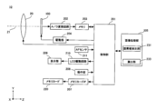
- FIG. 7 is a diagram illustrating the configuration of the digital camera 10.
- the digital camera 10 includes a photographic lens 20 as a photographic optical system, and guides a subject light beam incident along the optical axis 21 to the image sensor 100.
- the photographing lens 20 may be an interchangeable lens that can be attached to and detached from the digital camera 10.
- the digital camera 10 includes an image sensor 100, a control unit 201, an A / D conversion circuit 202, a memory 203, a drive unit 204, an image processing unit 205, a memory card IF 207, an operation unit 208, a display unit 209, an LCD drive circuit 210, and an AF.
- a sensor 211 is provided.
- the direction parallel to the optical axis 21 toward the image sensor 100 is defined as the Z-axis plus direction
- the direction toward the front of the drawing on the plane orthogonal to the Z-axis is the X-axis plus direction
- the upward direction on the drawing is Y.
- the axis is defined as the plus direction.
- the coordinate axes are displayed so that the orientation of each figure can be understood with reference to the coordinate axes in FIG.
- the photographing lens 20 is composed of a plurality of optical lens groups, and forms an image of a subject light flux from the scene in the vicinity of its focal plane.
- the photographic lens 20 is represented by a single virtual lens arranged in the vicinity of the pupil.
- the image sensor 100 is disposed near the focal plane of the photographic lens 20.
- the image sensor 100 is an image sensor such as a CCD or CMOS sensor in which a plurality of photoelectric conversion elements are two-dimensionally arranged.
- the image sensor 100 is controlled in timing by the drive unit 204, converts the subject image formed on the light receiving surface into an image signal, and outputs the image signal to the A / D conversion circuit 202.
- the A / D conversion circuit 202 converts the image signal output from the image sensor 100 into a digital image signal and outputs the digital image signal to the memory 203.
- the image processing unit 205 performs various image processing using the memory 203 as a work space, and generates image data. In particular, the image processing unit 205 extracts a pixel value from the target pixel position of the color image data and the parallax image data, and extracts a pixel value as color image data at the target pixel position using the extracted pixel value.
- a calculation unit 233 for calculating is provided. Details of each processing will be described later.
- the image processing unit 205 also has general image processing functions such as adjusting image data according to the selected image format.
- the generated image data is converted into a display signal by the LCD drive circuit 210 and displayed on the display unit 209.
- the data is recorded on the memory card 220 attached to the memory card IF 207.
- the AF sensor 211 is a phase difference sensor in which a plurality of distance measuring points are set with respect to the subject space, and detects the defocus amount of the subject image at each distance measuring point.
- a series of shooting sequences is started when the operation unit 208 receives a user operation and outputs an operation signal to the control unit 201.
- Various operations such as AF and AE accompanying the imaging sequence are executed under the control of the control unit 201.
- the control unit 201 analyzes the detection signal of the AF sensor 211 and executes focus control for moving a focus lens that constitutes a part of the photographing lens 20.
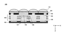
- FIG. 8 is a schematic diagram illustrating a cross section of the image sensor 100.
- the imaging element 100 is configured by arranging a micro lens 101, a color filter 102, an aperture mask 103, a wiring layer 105, and a photoelectric conversion element 108 in order from the subject side.
- the photoelectric conversion element 108 is configured by a photodiode that converts incident light into an electrical signal.
- a plurality of photoelectric conversion elements 108 are two-dimensionally arranged on the surface of the substrate 109.
- the image signal converted by the photoelectric conversion element 108, the control signal for controlling the photoelectric conversion element 108, and the like are transmitted / received via the wiring 106 provided in the wiring layer 105.
- an opening mask 103 having openings 104 provided in one-to-one correspondence with each photoelectric conversion element 108 is provided in contact with the wiring layer.
- the opening 104 is shifted for each corresponding photoelectric conversion element 108 so that the relative position is precisely determined.
- parallax occurs in the subject light beam received by the photoelectric conversion element 108 by the action of the opening mask 103 including the opening 104.
- the aperture mask 103 does not exist on the photoelectric conversion element 108 that does not generate parallax.
- an aperture mask 103 having an aperture 104 that does not limit the subject luminous flux incident on the corresponding photoelectric conversion element 108, that is, allows the entire incident luminous flux to pass therethrough is provided.
- the aperture 107 formed by the wiring 106 defines the incident light flux that is incident, so the wiring 106 is regarded as an aperture mask that allows the entire incident light flux that does not cause parallax to pass.
- the opening mask 103 may be arranged separately and independently corresponding to each photoelectric conversion element 108, or may be formed collectively for a plurality of photoelectric conversion elements 108 in the same manner as the manufacturing process of the color filter 102. .
- the color filter 102 is provided on the opening mask 103.
- the color filter 102 is a filter provided in a one-to-one correspondence with each photoelectric conversion element 108, which is colored so as to transmit a specific wavelength band to each photoelectric conversion element 108.
- the microlens 101 is provided on the color filter 102.
- the microlens 101 is a condensing lens for guiding more incident subject light flux to the photoelectric conversion element 108.
- the microlenses 101 are provided in a one-to-one correspondence with the photoelectric conversion elements 108.
- the optical axis of the microlens 101 is shifted so that more subject light flux is guided to the photoelectric conversion element 108. It is preferable.
- the arrangement position may be adjusted so that more specific subject light beam, which will be described later, is incident along with the position of the opening 104 of the opening mask 103.
- one unit of the aperture mask 103, the color filter 102, and the microlens 101 provided on a one-to-one basis corresponding to each photoelectric conversion element 108 is referred to as a pixel.
- a pixel provided with the opening mask 103 that generates parallax is referred to as a parallax pixel
- a pixel that is not provided with the opening mask 103 that generates parallax is referred to as a non-parallax pixel.
- the effective pixel area of the image sensor 100 is about 24 mm ⁇ 16 mm, the number of pixels reaches about 12 million.
- the microlens 101 may not be provided.
- the wiring layer 105 is provided on the side opposite to the photoelectric conversion element 108. Further, if the opening 104 of the opening mask 103 has a color component, the color filter 102 and the opening mask 103 can be formed integrally.
- the opening mask 103 and the wiring 106 are provided as separate bodies, but the wiring 106 may be responsible for the function of the opening mask 103 in the parallax pixels. That is, a prescribed opening shape is formed by the wiring 106, and the incident light beam is limited by the opening shape to guide only a specific partial light beam to the photoelectric conversion element 108. In this case, the wiring 106 that forms the opening shape is preferably closest to the photoelectric conversion element 108 in the wiring layer 105.
- the opening mask 103 may be formed by a permeation blocking film provided to overlap the photoelectric conversion element 108.
- the opening mask 103 is formed, for example, by sequentially laminating a SiN film and a SiO 2 film to form a permeation blocking film and removing a region corresponding to the opening 104 by etching.
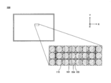
- FIG. 9 is a schematic diagram illustrating a state in which a part of the image sensor 100 is enlarged.
- the color arrangement of the color filter 102 is not considered until the reference is resumed later.
- the repetitive pattern described below may be considered as an adjacent pixel in the color filter 102 of the same color.
- the opening 104 of the opening mask 103 is provided with a relative shift with respect to each pixel.
- the openings 104 are provided at positions displaced from each other.
- the entire image sensor 100 has a two-dimensional and periodic array of photoelectric conversion element groups each including a set of six parallax pixels each having an aperture mask 103 that gradually shifts from the left side to the right side of the drawing. .
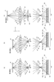
- FIG. 10 is a conceptual diagram illustrating the relationship between the parallax pixels and the subject.
- FIG. 10A shows a photoelectric conversion element group of a repetitive pattern 110t arranged at the center orthogonal to the photographing optical axis 21 in the image pickup element 100
- FIG. 10B shows a repetitive arrangement arranged in the peripheral portion.
- the photoelectric conversion element group of the pattern 110u is typically shown.
- the subject 30 in FIGS. 10A and 10B is in the in-focus position with respect to the photographic lens 20.
- FIG. 10C schematically shows the relationship when the subject 31 existing at the out-of-focus position with respect to the photographing lens 20 is captured corresponding to FIG.
- the subject luminous flux passes through the pupil of the photographic lens 20 and is guided to the image sensor 100.
- Six partial areas Pa to Pf are defined for the entire cross-sectional area through which the subject luminous flux passes. For example, in the pixel at the left end of the sheet of the photoelectric conversion element group constituting the repetitive patterns 110t and 110u, only the subject luminous flux emitted from the partial region Pf reaches the photoelectric conversion element 108 as can be seen from the enlarged view.
- the position of the opening 104f of the opening mask 103 is determined.
- the position of the opening 104e corresponding to the partial area Pe the position of the opening 104d corresponding to the partial area Pd, and the position of the opening 104c corresponding to the partial area Pc.
- the position of the opening 104b is determined corresponding to the partial area Pb
- the position of the opening 104a is determined corresponding to the partial area Pa.
- the position of the opening 104f is determined by the inclination of the principal ray Rf of the subject light beam (partial light beam) emitted from the partial region Pf, which is defined by the relative positional relationship between the partial region Pf and the leftmost pixel, for example. It may be said that it is established. Then, when the photoelectric conversion element 108 receives the subject luminous flux from the subject 30 existing at the in-focus position via the opening 104f, the subject luminous flux is coupled on the photoelectric conversion element 108 as shown by the dotted line. Image.
- the position of the opening 104e is determined by the inclination of the principal ray Re
- the position of the opening 104d is determined by the inclination of the principal ray Rd
- the position of the opening 104c is determined by the inclination of the principal ray Rc.
- the position of the opening 104b is determined by the inclination of the light ray Rb
- the position of the opening 104a is determined by the inclination of the principal ray Ra.
- the light beam emitted from the minute region Ot on the subject 30 that intersects the optical axis 21 among the subject 30 existing at the in-focus position passes through the pupil of the photographing lens 20.
- each pixel of the photoelectric conversion element group constituting the repetitive pattern 110t is reached. That is, each pixel of the photoelectric conversion element group constituting the repetitive pattern 110t receives the light beam emitted from one minute region Ot through the six partial regions Pa to Pf.
- the minute region Ot has an extent corresponding to the positional deviation of each pixel of the photoelectric conversion element group constituting the repetitive pattern 110t, it can be approximated to substantially the same object point.
- the luminous flux emitted from the minute region Ou on the subject 30 that is separated from the optical axis 21 among the subject 30 that exists at the in-focus position is reflected on the pupil of the photographing lens 20. It passes through and reaches each pixel of the photoelectric conversion element group constituting the repetitive pattern 110u. That is, each pixel of the photoelectric conversion element group constituting the repetitive pattern 110u receives a light beam emitted from one minute region Ou via each of the six partial regions Pa to Pf.
- the micro area Ou has an extent corresponding to the positional deviation of each pixel of the photoelectric conversion element group constituting the repetitive pattern 110u, but substantially the same object point. Can be approximated.
- the minute area captured by the photoelectric conversion element group differs according to the position of the repetitive pattern 110 on the image sensor 100, and each pixel constituting the photoelectric conversion element group Captures the same minute region through different partial regions.
- each repetitive pattern 110 corresponding pixels receive the subject luminous flux from the same partial area. That is, in the drawing, for example, the leftmost pixel of each of the repeated patterns 110t and 110u receives a partial light beam from the same partial region Pf.
- each of the parallax pixels arranged on the image sensor 100 includes one of six types of aperture masks.
- the subject luminous flux from the subject 31 present at the out-of-focus position passes through the six partial areas Pa to Pf of the pupil of the photographing lens 20 and reaches the image sensor 100.
- the subject light flux from the subject 31 existing at the out-of-focus position forms an image at another position, not on the photoelectric conversion element 108.
- the subject luminous flux forms an image on the subject 31 side with respect to the photoelectric conversion element 108.
- the subject luminous flux forms an image on the opposite side of the subject 31 from the photoelectric conversion element 108.
- the subject luminous flux radiated from the minute region Ot ′ among the subjects 31 existing at the out-of-focus position depends on which of the six partial regions Pa to Pf, the corresponding pixels in different sets of repetitive patterns 110.
- the subject luminous flux that has passed through the partial region Pd is incident on the photoelectric conversion element 108 having the opening 104d included in the repeated pattern 110t ′ as the principal ray Rd ′.
- the subject light beam that has passed through another partial region does not enter the photoelectric conversion element 108 included in the repetitive pattern 110t ′, and the repetitive pattern in the other repetitive pattern.
- the subject luminous flux reaching each photoelectric conversion element 108 constituting the repetitive pattern 110t ′ is a subject luminous flux radiated from different minute areas of the subject 31. That is, a subject luminous flux having a principal ray as Rd ′ is incident on 108 corresponding to the opening 104d, and the principal rays are incident on Ra + , Rb + , Rc + , Re to the photoelectric conversion elements 108 corresponding to the other openings. +, although subject light flux to Rf + is incident, these object light is a subject light flux emitted from different micro region of the object 31. Such a relationship is the same in the repeated pattern 110u arranged in the peripheral portion in FIG.
- the subject image A captured by the photoelectric conversion element 108 corresponding to the opening 104a and the subject image D captured by the photoelectric conversion element 108 corresponding to the opening 104d are: If the image is for the subject present at the in-focus position, there is no shift, and if the image is for the subject present at the out-of-focus position, there is a shift. Then, the direction and amount of the shift are determined by how much the subject existing at the out-of-focus position is shifted from the focus position and by the distance between the partial area Pa and the partial area Pd. That is, the subject image A and the subject image D are parallax images. Since this relationship is the same for the other openings, six parallax images are formed corresponding to the openings 104a to 104f.
- a parallax image is obtained by gathering together the outputs of pixels corresponding to each other in each of the repetitive patterns 110 configured as described above. That is, the output of the pixel that has received the subject light beam emitted from a specific partial area among the six partial areas Pa to Pf forms a parallax image.
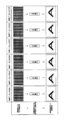
- FIG. 11 is a conceptual diagram illustrating processing for generating a parallax image.
- the figure shows, in order from the left column, the generation of the parallax image data Im_f generated by collecting the outputs of the parallax pixels corresponding to the opening 104f, the generation of the parallax image data Im_e by the output of the opening 104e, the opening State of generation of parallax image data Im_d by output of 104d, state of generation of parallax image data Im_c by output of opening 104c, state of generation of parallax image data Im_b by output of opening 104b, parallax by output of opening 104a
- the parallax image data Im_f is generated by the output of the opening 104f will be described.
- the repetitive pattern 110 composed of a group of photoelectric conversion elements including a set of six parallax pixels is arranged in a horizontal row. Therefore, the parallax pixels having the opening 104f are present every six pixels in the left-right direction and continuously in the vertical direction on the virtual imaging element 100 excluding the pixels without parallax. Each of these pixels receives the subject luminous flux from different microregions as described above. Therefore, when the outputs of these parallax pixels are collected and arranged, a parallax image is obtained.
- each pixel of the image sensor 100 according to the present embodiment is a square pixel, simply gathering results in the result that the number of pixels in the horizontal direction is reduced to 1/6, and vertically long image data is generated. End up. Therefore, by performing an interpolation process to obtain the number of pixels 6 times in the horizontal direction, the parallax image data Im_f is generated as an image with an original aspect ratio.
- the parallax image data before the interpolation processing is an image that is thinned by 1/6 in the horizontal direction, the resolution in the horizontal direction is lower than the resolution in the vertical direction. That is, it can be said that the number of generated parallax image data and the improvement in resolution are in a conflicting relationship.
- a specific interpolation process applied to this embodiment will be described later.
- parallax image data Im_e to parallax image data Im_a are obtained. That is, the digital camera 10 can generate a six-view parallax image having parallax in the horizontal direction.
- Im_af is image data obtained by calculating an arithmetic average between Im_f and Im_a in order to eliminate parallax.
- an arithmetic mean between Im_e and Im_b is taken as Im_be.
- Im_cd an arithmetic average between Im_d and Im_c.
- Im_cd an arithmetic average between Im_d and Im_c.
- the output image Im_out thus obtained is a 2D image without parallax from which the influence of the illuminance difference has been removed, and a wide blur width obtained by combining all the blur widths over 6 parallaxes, that is, a pixel with no parallax having a full aperture mask An image of the subject with the same blur width is obtained.
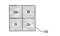
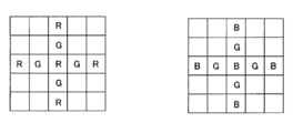
- FIG. 12 is a diagram for explaining the Bayer arrangement.
- the Bayer array is an array in which the green filter is assigned to the upper left and lower right pixels, the red filter is assigned to the lower left pixel, and the blue filter is assigned to the upper right pixel.
- the upper left pixel to which the green filter is assigned is the Gb pixel
- the lower right pixel to which the green filter is assigned is the Gr pixel.
- a pixel to which a red filter is assigned is an R pixel
- a pixel to which blue is assigned is a B pixel.
- a horizontal direction in which Gb pixels and B pixels are arranged is defined as Gb row, and a horizontal direction in which R pixels and Gr pixels are arranged is defined as Gr row.
- a vertical direction in which Gb pixels and R pixels are arranged is a Gb column, and a vertical direction in which B pixels and Gr pixels are arranged is a Gr column.
- a huge number of repetitive patterns 110 can be set for such an array of the color filters 102 depending on what color pixels the parallax pixels and non-parallax pixels are allocated to. For example, if many non-parallax pixels are allocated, high-resolution 2D image data is obtained, and if all pixels of RGB are equally allocated, high-quality 2D image data with little color shift is obtained. . However, in this case, since the number of parallax pixels is relatively small, the image quality is degraded as a 3D image including a plurality of parallax images.
- a repetitive pattern 110 having various characteristics is set depending on which pixel is a parallax pixel or a non-parallax pixel.
- each of the parallax pixels is a parallax Lt pixel that is eccentric to the left side of the opening 104 and a parallax Rt pixel that is also eccentric to the right side.
- the two viewpoint parallax images output from such parallax pixels realize so-called stereoscopic vision.
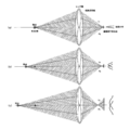
- FIG. 13 is a diagram for explaining the concept of defocusing in a pixel without parallax.
- FIG. 13A when an object point that is a subject exists at the focal position, the subject luminous flux that reaches the image sensor light receiving surface through the lens pupil is steep with the pixel at the corresponding image point as the center. The light intensity distribution is shown.
- the subject luminous flux exhibits a gentle light intensity distribution on the light receiving surface of the image sensor as compared with the case where the object point exists at the focal position. . That is, the output value at the pixel of the corresponding image point is lowered, and a distribution having output values up to the peripheral pixels is shown.
- the subject luminous flux when the object point further deviates from the focal position, the subject luminous flux exhibits a gentler light intensity distribution on the image sensor light receiving surface.
- the output value at the pixel of the corresponding image point further decreases, and a distribution having output values up to the surrounding pixels is shown.
- FIG. 14 is a diagram for explaining the concept of defocusing in a parallax pixel.
- the parallax Lt pixel and the parallax Rt pixel receive the subject luminous flux that arrives from one of the two parallax virtual pupils set as the optical axis target as a partial region of the lens pupil.
- the peak of the light intensity distribution indicated by the parallax Lt pixel corresponds to the image point, compared to the case where the object point exists at the focal position. Appearing at a position away from the pixel in one direction, and its output value decreases. In addition, the width of the pixel having the output value is increased. The peak of the light intensity distribution indicated by the parallax Rt pixel appears at a position away from the pixel corresponding to the image point in the opposite direction to the one direction in the parallax Lt pixel and at an equal distance, and the output value similarly decreases. Similarly, the width of the pixel having the output value is increased.
- the same light intensity distribution that is gentler than that in the case where the object point exists at the focal position appears at an equal distance from each other. Further, as shown in FIG. 14C, when the object point is further deviated from the focal position, the same light intensity distribution that is more gentle than the state of FIG. 14B appears further apart. . That is, it can be said that the amount of blur and the amount of parallax increase as the object point deviates from the focal position.
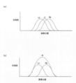
- FIG. 13 is a graph showing the change in the light intensity distribution described in FIG. 13 and the change in the light intensity distribution described in FIG.
- the horizontal axis represents the pixel position, and the center position is the pixel position corresponding to the image point.
- the vertical axis represents the output value of each pixel. Since this output value is substantially proportional to the light intensity, it is shown as the light intensity in the figure.
- FIG. 15A is a graph showing changes in the light intensity distribution described in FIG.
- a distribution curve 1801 represents the light intensity distribution corresponding to FIG. 13A and shows the steepest state.
- a distribution curve 1802 represents a light intensity distribution corresponding to FIG. 13B, and a distribution curve 1803 represents a light intensity distribution corresponding to FIG.
- the peak value gradually decreases and has a broadening.
- FIG. 15B is a graph showing changes in the light intensity distribution described in FIG.
- a distribution curve 1804 and a distribution curve 1805 represent the light intensity distribution of the parallax Lt pixel and the light intensity distribution of the parallax Rt pixel in FIG. As can be seen from the figure, these distributions have a line-symmetric shape with respect to the center position. Further, a combined distribution curve 1806 obtained by adding them shows a similar shape to the distribution curve 1802 in FIG. 13B, which is in the same defocused state as in FIG. 14B.
- the distribution curve 1807 and the distribution curve 1808 represent the light intensity distribution of the parallax Lt pixel and the light intensity distribution of the parallax Rt pixel in FIG. As can be seen from the figure, these distributions are also symmetrical with respect to the center position. Further, a combined distribution curve 1809 obtained by adding them shows a similar shape to the distribution curve 1803 in FIG. 13C, which is in the same defocused state as in FIG. 14C.
- FIG. 16 is a diagram illustrating the opening shape of the opening 104 when there are two types of parallax pixels.
- the shape of the opening 104l of the parallax Lt pixel and the shape of the opening 104r of the parallax Rt pixel are obtained by dividing the shape of the opening 104n of the non-parallax pixel by the center line 322, respectively.
- the example which is the same is shown. That is, in FIG. 16A, the area of the opening 104n of the non-parallax pixel is the sum of the area of the opening 104l of the parallax Lt pixel and the area of the opening 104r of the parallax Rt pixel.
- the opening 104n of the non-parallax pixel is referred to as a full-opening opening, and the opening 104l and the opening 104r are referred to as half-opening openings.
- the opening is directed to the reference direction.
- the opening 104l of the parallax Lt pixel and the opening 104r of the parallax Rt pixel are displaced in opposite directions with respect to a virtual center line 322 passing through the center (pixel center) of the corresponding photoelectric conversion element 108. Yes.
- the opening 104l of the parallax Lt pixel and the opening 104r of the parallax Rt pixel each generate parallax in one direction with respect to the reference direction and in the other direction opposite to the one direction.
- FIG. 16B shows the light intensity distribution when the object point is deviated from the focal position in the pixel having each opening shown in FIG.
- the curve Lt corresponds to the distribution curve 1804 in FIG. 15B
- the curve Rt corresponds to the distribution curve 1805 in FIG.
- a curve N corresponds to a pixel without parallax, and shows a similar shape to the combined distribution curve 1806 in FIG.
- Each of the openings 104n, 104l, and 104r has an aperture stop function. Therefore, the blur width of the non-parallax pixel having the opening 104n having an area double the opening 104l (opening 104r) is the Lt pixel and the parallax Rt pixel indicated by the combined distribution curve 1806 in FIG. It is about the same as the blur width of the added curve.
- FIG. 16C shows an example in which the shape of the opening 104l of the parallax Lt pixel, the shape of the opening 104r of the parallax Rt pixel, and the shape of the opening 104c of the parallax C pixel are all the same shape.
- the parallax C pixel is a pixel having no eccentricity.
- the parallax C pixel is a parallax pixel that outputs a parallax image, in that only the subject luminous flux having the central portion of the pupil as a partial region is guided to the photoelectric conversion element 108.
- a pixel having an opening corresponding to the reference direction is defined as a non-parallax pixel.
- the parallax C pixel in FIG. 16C having an opening at the center of the photoelectric conversion element is the non-parallax pixel as in the non-parallax pixel in FIG.
- the opening 104l, the opening 104r, and the opening 104c are half the area of the opening 104n illustrated in FIG.
- each of the openings 104 l and 104 r is in contact with a virtual center line 322 that passes through the center (pixel center) of the photoelectric conversion element 108.
- FIG. 16D shows the light intensity distribution when the object point is deviated from the focal position in the pixel having each opening shown in FIG.
- the curve Lt corresponds to the distribution curve 1804 in FIG. 15B
- the curve Rt corresponds to the distribution curve 1805 in FIG.
- Each of the openings 104c, 104l, and 104r has a function of an aperture stop. Therefore, the blur width of the parallax C pixel having the opening 104c having the same shape and the same area as the opening 104l and the opening 104r is approximately the same as the blur width of the parallax Lt pixel and the parallax Rt pixel.
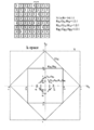
- FIG. 17 is a diagram illustrating an example of the repeating pattern 110 when there are two types of parallax pixels.
- the coordinate system of the digital camera 10 is defined by the X axis, the Y axis, and the Z axis.
- the x axis is defined in the right direction and the y axis is defined in the lower direction with reference to the left and upper end pixels. .
- the same four pixels as the Bayer array are used as the repeated pattern 110.
- the effective pixel area of the image sensor 100 is periodically arranged in the vertical and horizontal directions. In other words, the imaging device 100 uses a repetitive pattern 110 indicated by a thick line in the drawing as a basic lattice.
- the R pixel and the B pixel are non-parallax pixels, and the Gb pixel is assigned to the parallax L pixel and the Gr pixel is assigned to the parallax R pixel.
- the opening 104 is defined so that the parallax Lt pixel and the parallax Rt pixel included in the same repetitive pattern 110 receive the light beam emitted from the same minute region when the subject is in the in-focus position. .
- the non-parallax pixel is the opening portion of the full opening
- the parallax Lt pixel and the parallax Rt pixel are the opening portions of the half opening.
- the pixel pitch is a.
- the Gb pixel and the Gr pixel which are green pixels having high visibility, are used as the parallax pixels, it is expected to obtain a parallax image with high contrast.
- the Gb pixel and the Gr pixel which are the same green pixels are used as the parallax pixels, it is easy to perform a conversion operation from these two outputs to an output having no parallax, and the output of the R pixel and the B pixel which are non-parallax pixels is high. High-quality 2D image data can be generated.
- the left side is used as a virtual output of the parallax Lt pixel and the parallax Rt pixel that do not actually exist as the pixels of the image sensor 100 and have any of RGB color filters.
- the color image data of the viewpoint and the right viewpoint is acquired by a relatively simple process by a conversion operation.
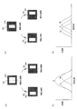
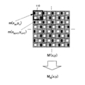
- FIG. 1 (bottom) is a diagram showing the resolution related to the spatial frequency of an image captured by an image sensor employing the repetitive pattern 110 shown in FIG.
- f shows a frequency.
- the frequency resolution region is described by a first Brillouin zone representing a unit cell (Wigner-Zeilz cell) in a reciprocal lattice space.
- k y [ ⁇ ⁇ / a, + ⁇ / a] in the range of resolution. That is, the range surrounded by the dotted line is the limit resolution frequency of the image.
- the color filter and the aperture mask are arranged so as to overlap one sensor surface. Since the information captured by one sensor surface is constant, the amount of information is reduced by dividing the functions.
- the number of pixels without parallax is relatively reduced, and thus the amount of information obtained by the pixels without parallax is reduced.
- the color filter and the amount of individual information is reduced by the amount of R, G, B.
- the limit resolution frequency of the image does not reach the inherent Nyquist frequency.
- Image G Rt of the G component of the right-side perspective, the image R N of the R component of no parallax intermediate viewpoint, the image B N of the B component of intermediate viewpoint no disparity is the same.
- the image processing unit 205 performs processing for increasing the resolution in order to compensate for the amount of information reduced by dividing the functions.
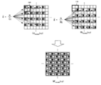
- the G Lt pixel and G Rt pixel is parallax pixels, by replacing a virtual parallax without pixel G N, to produce a Bayer array of no parallax pixels only.
- an original Nyquist frequency k x [ ⁇ ⁇ / a, + ⁇ / a]
- k y [ ⁇ ⁇ / a, + ⁇ / a) as an intermediate image without parallax. ] Can be generated.
- each pixel in the pixel array shown in FIG. 17 includes various parallax pixels and non-parallax pixels when focusing on the opening 104, and various R pixels, G pixels, and B pixels when focusing on the color filter 102. Characterized in combination. Therefore, even if the outputs of the image sensor 100 are aligned with the pixel arrangement, they are not image data representing a specific image. That is, only when the pixel outputs of the image sensor 100 are separated and collected for each pixel group characterized by the same, image data representing one image corresponding to the feature is formed. For example, as already described with reference to FIG.
- the image processing unit 205 receives mosaic image data M mosaic (x, y), which is raw image data in which output values are arranged in the order of pixel arrangement of the image sensor 100.
- M mosaic x, y
- an image lacking at least one of R, G, and B information in each pixel is referred to as a mosaic image
- data forming the mosaic image is referred to as mosaic image data.
- At least one piece of information of R, G, and B is missing in each pixel, if it is not handled as an image in the first place, for example, if image data is composed of pixel values of monochrome pixels, it is treated as a mosaic image. Absent.
- Each output value is a linear gradation value proportional to the amount of light received by each photoelectric conversion element of the image sensor 100.
- the image processing unit 205 performs gain correction for matching the overall brightness between the left and right at this stage.
- the illuminance of light incident on the left parallax pixel and the illuminance of light incident on the right parallax pixel have a large difference not only in the relative distribution between the left and right but also in the average signal level of the entire image. This is because it occurs.
- the gain correction for matching the overall brightness between the left and right is called global gain correction.
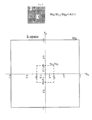
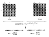
- FIG. 18 is a diagram for explaining the calculation of the gain value.
- the mosaic image data of the left parallax pixel of the G component is Lt mosaic (x, y)
- the mosaic image data of the right parallax pixel of the G component is Rt mosaic ( x, y)
- FIG. 18 only the left and right parallax pixels are extracted and illustrated.
- the pixel types are described so that the types of pixels can be understood in accordance with the example of FIG. 17, but output values corresponding to the respective pixels are actually arranged.
- FIG. 19 is a diagram for explaining gain correction.
- the calculation unit 233 of the image processing unit 205 calculates the Lt mosaic (x, y) and Rt mosaic (x, y) pixels as illustrated.
- Gain correction is performed using the gain value. Specifically, gain correction for the left parallax pixel is performed by the following (Equation 1), and gain correction for the right parallax pixel is performed by (Equation 2).
- the mosaic image data M ′ mosaic (x, y) the mosaic image data of the G component left parallax pixel is the Lt ′ mosaic (x, y), the mosaic image data of the G component right parallax pixel.
- the calculation unit 233 of the image processing unit 205 performs mosaic image data M ′ mosaic in which the left parallax pixel and the right parallax pixel in M mosaic (x, y) are each corrected with one gain coefficient, as illustrated. (X, y) can be generated.
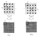
- the image processing unit 205 generates a left parallax image and a right parallax image with low spatial frequency resolution as temporary parallax images.
- FIG. 20 is a diagram for explaining generation of a temporary parallax image.
- the image processing unit 205 separates the mosaic image data M ′ mosaic (x, y) into a plurality of plane data. Each plane data at this point has an output value only at a pixel position where the output value exists in the RAW original image data. Therefore, the image processing unit 205 performs an interpolation process based on each plane data, and generates plane data in which vacancies are filled.
- the left side of the upper diagram shows Lt ′ mosaic (x, y), which is plain data obtained by extracting only the left parallax pixels from the mosaic image data M ′ mosaic (x, y), and the right side shows the right parallax.
- Lt ′ mosaic (x, y) which is plain data obtained by extracting only the left parallax pixels from the mosaic image data M ′ mosaic (x, y)
- Rt'mosaic (x, y) which is the plane data which extracted only the pixel.
- it describes so that the kind of pixel may be understood according to the example of FIG. 17, but actually the output value corresponding to each pixel is arranged.
- the calculation unit 233 of the image processing unit 205 uses the pixel values that have become empty grids as the pixel values of the surrounding left parallax pixels. And is calculated by interpolation processing. For example, the pixel value of the empty lattice P L1 is calculated by averaging pixel values of four left parallax pixels adjacent in the diagonal direction. The calculation unit 233 of the image processing unit 205 averages the pixel values of the surrounding left parallax pixels and performs an interpolation process on all the empty grids, as shown in the lower left diagram of FIG. Lt ′ (x, y) that is plane data in which the child is filled is generated. Note that the calculation unit 233 of the image processing unit 205 may further perform interpolation processing using the pixel values calculated by the interpolation processing, or perform interpolation using only output values existing at the stage of the RAW original image data. Processing may be performed.
- the calculation unit 233 of the image processing unit 205 uses the pixel values that have become empty grids as peripheral right parallax pixels.
- the pixel value is calculated by interpolation processing.
- the pixel value of the empty grid PR1 is calculated by averaging pixel values of four right parallax pixels adjacent in the diagonal direction.
- the calculation unit 233 of the image processing unit 205 averages the pixel values of the surrounding right parallax pixels and performs interpolation processing for all the empty grids, as shown in the lower right diagram of FIG. Rt ′ (x, y) that is plane data in which the child is filled is generated.
- the calculation unit 233 of the image processing unit 205 performs gain correction on each pixel of Lt ′ (x, y) using the calculated gain value, and similarly, Rt ′ (x, y ), The gain correction is performed using the calculated gain value.
- the gain correction using the gain value calculated for each pixel in this way is referred to as local gain correction in contrast to the above-described global gain correction.
- FIG. 21 is a diagram for explaining the calculation of the gain value.
- the calculation unit 233 of the image processing unit 205 calculates an average value for each pixel from Lt ′ (x, y) and Rt ′ (x, y).
- arithmetic mean and geometric mean.
- an arithmetic average is employed so that the blur width of the subject image in the non-parallax pixel of the G component where the parallax disappears matches the blur width of the subject image of the pixel without parallax.
- the calculation unit 233 of the image processing unit 205 calculates the average value by the following (Equation 3).
- FIG. 22 is a diagram for explaining the local gain correction.
- the calculation unit 233 of the image processing unit 205 includes m (x m , y n ) and m (x) calculated by (Equation 3), respectively, as illustrated in FIG.
- Local gain correction can be performed simply by replacing with ( m + 1 , y n + 1 ). In this sense, it can be said that the local gain correction is a modulation process for eliminating the parallax. Thereby, it is possible to obtain a Bayer array in which the pixel values of the parallax Gb pixel and the parallax Gr pixel are replaced with the pixel values of the non-parallax G pixel.
- the calculation unit 233 of the image processing unit 205 generates M N (x, y) by replacing the pixel values of all the left and right parallax pixels with the corresponding average values calculated in (Equation 3). Note that local gain correction may be performed not on all the pixels of Lt ′ (x, y) and Rt ′ (x, y) but on the pixels corresponding to the positions of the left parallax pixel and the right parallax pixel in the Bayer array. Good.
- the image processing unit 205 uses, as an intermediate image data, non-parallax color image data in which each pixel has a resolution from N N (x, y) to the Nyquist frequency using existing color interpolation technology. Generate.
- FIG. 23 is a diagram for explaining interpolation of the G component.
- the G color interpolation is calculated with reference to the pixel in the drawing with respect to the position [i, j] of the center R pixel shown in the left drawing of FIG.
- the pixel position when G color interpolation is performed on the position of the B pixel is shown in the right diagram of FIG.
- the image processing unit 205 performs Lt ′ (x, y), Rt ′ (x, y), R N (x, y), G N (x, y), B N (x, y). ) Color image data for the left viewpoint and color image data for the right viewpoint are generated. Specifically, the image processing unit 205 generates left and right color image data by superimposing the parallax component of the temporary parallax image on the non-parallax image. This generation process is called parallax modulation process.
- the color image data of the left viewpoint includes R Lt (x, y) that is red plane data corresponding to the left viewpoint, G Lt (x, y) that is green plane data, and B Lt (x, y) that is blue plane data.
- y three color parallax plane data.
- the color image data of the right viewpoint is red plane data R Rt (x, y) corresponding to the right viewpoint, green plane data G Rt (x, y), and blue plane data B Rt. It is composed of three color parallax plane data of (x, y).
- FIG. 24 is a diagram for explaining color parallax plane data generation processing.
- a process for generating R Lt (x, y) and R Rt (x, y), which are red parallax planes among the color parallax planes, will be described.
- red, green and blue are used as primary colors constituting the color of the subject image.
- four or more colors including amber color may be used as primary colors.
- red, green, and blue three primary colors that are complementary colors of yellow, magenta, and cyan can be used.
- the pixel value extraction unit 231 and the calculation unit 233 included in the image processing unit 205 have described the respective processes as functions of the respective components constituting the digital camera 10.
- the control program that operates the control unit 201 and the image processing unit 205 can cause each hardware component of the digital camera 10 to function as a component that executes the above-described processing.
- these processes for generating color image data may be performed not by the digital camera 10 but by an external device such as a personal computer.
- an external device such as a personal computer functions as an image processing apparatus.
- the image processing apparatus acquires RAW original image data and generates color image data.
- the image processing apparatus When the RAW original image data is acquired, the image processing apparatus also executes the above-described plane separation processing and plane data interpolation processing.
- the image processing apparatus may acquire plane data that has undergone interpolation processing on the imaging apparatus side.
- a program related to the above-described processing can be provided through a recording medium such as a CD-ROM or a data signal such as the Internet.
- the geometric average is used for the purpose of making the blur width common in the operation of taking the average between the signal plane in which the parallax disappears between the left and right and the imaging signal plane of the non-parallax pixel.
- the weight for the pixel value and the distribution of the weight for the average value were equal.
- the number of parallax pixels is smaller than the number of non-parallax pixels.
- the resolution of the parallax image is lower than the resolution of the image without parallax.
- the resolution of the obtained image decreases as a whole due to the influence of the resolution of the parallax image. Therefore, it is necessary to devise as close as possible to the resolution of an image without parallax. Therefore, it is preferable to take a geometric average in consideration of the density ratio between the non-parallax pixels and the parallax pixels in the pixel array on the image sensor.
- a method of selecting an arithmetic mean As described above, there are two methods for eliminating the parallax between the left and right, a method of selecting an arithmetic mean and a method of selecting a geometric mean. If all non-parallax pixels have a mask area with a full aperture, the arithmetic average type should be selected so that the blur width of the subject image with the parallax disappeared between the left and right matches the blur width of the full aperture. .
- the following a) shows the case where the arithmetic mean type is selected.
- the geometric average type may be selected so that the blur width of the subject image whose parallax disappeared between the left and right coincides with the blur width of the half aperture.
- the following b) shows the case where the geometric average type is selected.
- the following b) shows the parallax modulation using the geometric mean as a reference point.
- the following a) shows a case where the arithmetic mean type is selected as a method for eliminating the parallax between the left and right.
- the following b) shows a case where the geometric average type is selected as a method of eliminating the parallax between the left and right.
- An arithmetic average may be taken in consideration of the density ratio between the non-parallax pixel and the parallax pixel in the pixel array on the image sensor. This is particularly effective when the operations described in the above-described embodiments are realized by hardware.
- an average is taken between the signal plane in which the parallax disappears between the left and right and the imaging signal plane of the non-parallax pixel.
- an arithmetic average can be similarly obtained even when a monochrome imaging element is used.
- the following a) shows a case where the arithmetic mean type is selected as a method for eliminating the parallax between the left and right.
- the following b) shows a case where the geometric average type is selected as a method of eliminating the parallax between the left and right.
Priority Applications (2)
| Application Number | Priority Date | Filing Date | Title |
|---|---|---|---|
| CN201380014377.6A CN104170377B (zh) | 2012-03-16 | 2013-03-14 | 图像处理装置、摄像装置 |
| US14/482,397 US10027942B2 (en) | 2012-03-16 | 2014-09-10 | Imaging processing apparatus, image-capturing apparatus, and storage medium having image processing program stored thereon |
Applications Claiming Priority (4)
| Application Number | Priority Date | Filing Date | Title |
|---|---|---|---|
| JP2012-061012 | 2012-03-16 | ||
| JP2012061012 | 2012-03-16 | ||
| JP2012-183511 | 2012-08-22 | ||
| JP2012183511A JP6131546B2 (ja) | 2012-03-16 | 2012-08-22 | 画像処理装置、撮像装置および画像処理プログラム |
Related Child Applications (1)
| Application Number | Title | Priority Date | Filing Date |
|---|---|---|---|
| US14/482,397 Continuation US10027942B2 (en) | 2012-03-16 | 2014-09-10 | Imaging processing apparatus, image-capturing apparatus, and storage medium having image processing program stored thereon |
Publications (1)
| Publication Number | Publication Date |
|---|---|
| WO2013136809A1 true WO2013136809A1 (ja) | 2013-09-19 |
Family
ID=49160732
Family Applications (1)
| Application Number | Title | Priority Date | Filing Date |
|---|---|---|---|
| PCT/JP2013/001746 WO2013136809A1 (ja) | 2012-03-16 | 2013-03-14 | 画像処理装置、撮像装置および画像処理プログラム |
Country Status (4)
| Country | Link |
|---|---|
| US (1) | US10027942B2 (zh) |
| JP (1) | JP6131546B2 (zh) |
| CN (1) | CN104170377B (zh) |
| WO (1) | WO2013136809A1 (zh) |
Cited By (1)
| Publication number | Priority date | Publication date | Assignee | Title |
|---|---|---|---|---|
| CN112736101A (zh) * | 2019-10-28 | 2021-04-30 | 豪威科技股份有限公司 | 在多个子像素之间具有共享微透镜的图像传感器 |
Families Citing this family (9)
| Publication number | Priority date | Publication date | Assignee | Title |
|---|---|---|---|---|
| CN104322061B (zh) * | 2012-06-22 | 2017-01-18 | 株式会社尼康 | 图像处理装置、摄像装置及图像处理方法 |
| WO2014024500A1 (ja) | 2012-08-10 | 2014-02-13 | 株式会社ニコン | 画像処理方法、画像処理装置、撮像装置および画像処理プログラム |
| WO2014156202A1 (ja) | 2013-03-29 | 2014-10-02 | 株式会社ニコン | 画像処理装置、撮像装置および画像処理プログラム |
| JP5982601B2 (ja) * | 2014-03-18 | 2016-08-31 | 富士フイルム株式会社 | 撮像装置及び合焦制御方法 |
| JP6405243B2 (ja) * | 2014-03-26 | 2018-10-17 | キヤノン株式会社 | 焦点検出装置及びその制御方法 |
| JP6354838B2 (ja) | 2014-04-04 | 2018-07-11 | 株式会社ニコン | 撮像素子、撮像装置および画像処理装置 |
| JP6900161B2 (ja) * | 2016-09-14 | 2021-07-07 | キヤノン株式会社 | 焦点調節装置及び撮像装置 |
| JP6723546B2 (ja) * | 2016-10-07 | 2020-07-15 | 株式会社ディー・ディー・エス | 情報処理プログラム及び情報処理装置 |
| CN110176280B (zh) * | 2019-05-10 | 2023-06-06 | 北京大学深圳研究生院 | 一种描述材料晶体结构的方法及其应用 |
Citations (3)
| Publication number | Priority date | Publication date | Assignee | Title |
|---|---|---|---|---|
| JP2003523646A (ja) * | 1999-02-25 | 2003-08-05 | ヴィジョンセンス リミテッド | 光学装置 |
| JP2010081609A (ja) * | 2008-09-25 | 2010-04-08 | Samsung Electronics Co Ltd | 立体イメージセンサ |
| WO2012002297A1 (ja) * | 2010-06-30 | 2012-01-05 | 富士フイルム株式会社 | 撮像装置および撮像方法 |
Family Cites Families (25)
| Publication number | Priority date | Publication date | Assignee | Title |
|---|---|---|---|---|
| US6836572B2 (en) | 1998-06-01 | 2004-12-28 | Nikon Corporation | Interpolation processing apparatus and recording medium having interpolation processing program recorded therein |
| JP4599672B2 (ja) | 1999-12-21 | 2010-12-15 | 株式会社ニコン | 補間処理装置および補間処理プログラムを記録した記録媒体 |
| JP3985679B2 (ja) | 2001-01-25 | 2007-10-03 | 株式会社ニコン | 画像処理方法、画像処理プログラム、画像処理装置 |
| JP2003007994A (ja) * | 2001-06-27 | 2003-01-10 | Konica Corp | 固体撮像素子、立体カメラ装置及び測距装置 |
| WO2004112401A1 (ja) | 2003-06-12 | 2004-12-23 | Nikon Corporation | 画像処理方法、画像処理プログラム、画像処理装置 |
| EP1781043B1 (en) * | 2004-07-07 | 2013-01-23 | Nikon Corporation | Image processor and computer program product |
| WO2007007878A1 (ja) * | 2005-07-14 | 2007-01-18 | Nikon Corporation | 画像処理装置および画像処理方法 |
| US8274715B2 (en) * | 2005-07-28 | 2012-09-25 | Omnivision Technologies, Inc. | Processing color and panchromatic pixels |
| US7999873B2 (en) * | 2005-11-22 | 2011-08-16 | Panasonic Corporation | Imaging device with plural lenses and imaging regions |
| US20090051790A1 (en) * | 2007-08-21 | 2009-02-26 | Micron Technology, Inc. | De-parallax methods and apparatuses for lateral sensor arrays |
| WO2009066770A1 (ja) | 2007-11-22 | 2009-05-28 | Nikon Corporation | デジタルカメラおよびデジタルカメラシステム |
| KR101697598B1 (ko) * | 2008-10-27 | 2017-02-01 | 엘지전자 주식회사 | 가상 뷰 이미지 합성 방법 및 장치 |
| JP5332978B2 (ja) * | 2009-07-07 | 2013-11-06 | ソニー株式会社 | 立体表示装置 |
| US8508580B2 (en) * | 2009-07-31 | 2013-08-13 | 3Dmedia Corporation | Methods, systems, and computer-readable storage media for creating three-dimensional (3D) images of a scene |
| US8611654B2 (en) * | 2010-01-05 | 2013-12-17 | Adobe Systems Incorporated | Color saturation-modulated blending of exposure-bracketed images |
| JP5470458B2 (ja) | 2010-06-30 | 2014-04-16 | 富士フイルム株式会社 | 撮像装置、画像処理装置および画像処理方法 |
| CN102934024B (zh) | 2010-06-30 | 2015-07-22 | 富士胶片株式会社 | 摄像装置及摄像方法 |
| CN103081457B (zh) * | 2010-08-24 | 2016-04-13 | 富士胶片株式会社 | 固态成像装置 |
| JP5513326B2 (ja) * | 2010-09-07 | 2014-06-04 | キヤノン株式会社 | 撮像素子及び撮像装置 |
| EP2618585B1 (en) | 2010-09-13 | 2016-07-27 | Fujifilm Corporation | Monocular 3d-imaging device, shading correction method for monocular 3d-imaging device, and program for monocular 3d-imaging device |
| WO2012039346A1 (ja) | 2010-09-22 | 2012-03-29 | 富士フイルム株式会社 | 立体撮像装置およびシェーディング補正方法 |
| KR20120049636A (ko) * | 2010-11-09 | 2012-05-17 | 삼성전자주식회사 | 영상 처리 장치 및 방법 |
| US9532033B2 (en) | 2010-11-29 | 2016-12-27 | Nikon Corporation | Image sensor and imaging device |
| US8742309B2 (en) * | 2011-01-28 | 2014-06-03 | Aptina Imaging Corporation | Imagers with depth sensing capabilities |
| CN104185983B (zh) | 2012-03-16 | 2016-10-26 | 株式会社尼康 | 摄像元件、摄像装置以及摄像系统 |
-
2012
- 2012-08-22 JP JP2012183511A patent/JP6131546B2/ja active Active
-
2013
- 2013-03-14 CN CN201380014377.6A patent/CN104170377B/zh active Active
- 2013-03-14 WO PCT/JP2013/001746 patent/WO2013136809A1/ja active Application Filing
-
2014
- 2014-09-10 US US14/482,397 patent/US10027942B2/en active Active
Patent Citations (3)
| Publication number | Priority date | Publication date | Assignee | Title |
|---|---|---|---|---|
| JP2003523646A (ja) * | 1999-02-25 | 2003-08-05 | ヴィジョンセンス リミテッド | 光学装置 |
| JP2010081609A (ja) * | 2008-09-25 | 2010-04-08 | Samsung Electronics Co Ltd | 立体イメージセンサ |
| WO2012002297A1 (ja) * | 2010-06-30 | 2012-01-05 | 富士フイルム株式会社 | 撮像装置および撮像方法 |
Cited By (2)
| Publication number | Priority date | Publication date | Assignee | Title |
|---|---|---|---|---|
| CN112736101A (zh) * | 2019-10-28 | 2021-04-30 | 豪威科技股份有限公司 | 在多个子像素之间具有共享微透镜的图像传感器 |
| CN112736101B (zh) * | 2019-10-28 | 2023-10-17 | 豪威科技股份有限公司 | 在多个子像素之间具有共享微透镜的图像传感器 |
Also Published As
| Publication number | Publication date |
|---|---|
| US20150062307A1 (en) | 2015-03-05 |
| CN104170377B (zh) | 2017-03-08 |
| JP6131546B2 (ja) | 2017-05-24 |
| US10027942B2 (en) | 2018-07-17 |
| JP2013219737A (ja) | 2013-10-24 |
| CN104170377A (zh) | 2014-11-26 |
Similar Documents
| Publication | Publication Date | Title |
|---|---|---|
| JP6131546B2 (ja) | 画像処理装置、撮像装置および画像処理プログラム | |
| JP5904281B2 (ja) | 画像処理方法、画像処理装置、撮像装置および画像処理プログラム | |
| JP5804055B2 (ja) | 画像処理装置、画像処理方法およびプログラム | |
| EP2845167A1 (en) | CAMERA MODULES PATTERNED WITH pi FILTER GROUPS | |
| JP6131545B2 (ja) | 画像処理装置、撮像装置および画像処理プログラム | |
| JP6003983B2 (ja) | 画像処理装置、撮像装置および画像処理プログラム | |
| WO2013136819A1 (ja) | 撮像素子、撮像装置および撮像システム | |
| US9544570B2 (en) | Three-dimensional image pickup apparatus, light-transparent unit, image processing apparatus, and program | |
| WO2013161313A1 (ja) | 画像処理装置、撮像装置および画像処理プログラム | |
| JP5979134B2 (ja) | 画像処理装置および画像処理プログラム | |
| JP5942984B2 (ja) | 画像処理装置、撮像装置および画像処理プログラム | |
| WO2013057859A1 (ja) | 撮像素子 | |
| JP6692749B2 (ja) | マルチスペクトルカメラ | |
| JP5978736B2 (ja) | 画像処理装置、撮像装置および画像処理プログラム | |
| JP5979137B2 (ja) | 撮像装置および撮像装置の制御プログラム | |
| JP5874334B2 (ja) | 画像処理装置、撮像装置、画像処理プログラムおよび撮像装置の制御プログラム | |
| JP5978737B2 (ja) | 画像処理装置、撮像装置および画像処理プログラム | |
| JP5978738B2 (ja) | 画像処理装置、撮像装置および画像処理プログラム | |
| JP6205770B2 (ja) | 撮像素子および撮像システム | |
| JP5978735B2 (ja) | 画像処理装置、撮像装置および画像処理プログラム | |
| JP2013090265A (ja) | 画像処理装置および画像処理プログラム | |
| JP2013150055A (ja) | 画像処理装置、画像処理方法、及び、プログラム |
Legal Events
| Date | Code | Title | Description |
|---|---|---|---|
| 121 | Ep: the epo has been informed by wipo that ep was designated in this application |
Ref document number: 13761494 Country of ref document: EP Kind code of ref document: A1 |
|
| NENP | Non-entry into the national phase |
Ref country code: DE |
|
| 122 | Ep: pct application non-entry in european phase |
Ref document number: 13761494 Country of ref document: EP Kind code of ref document: A1 |