WO2013136809A1 - 画像処理装置、撮像装置および画像処理プログラム - Google Patents
画像処理装置、撮像装置および画像処理プログラム Download PDFInfo
- Publication number
- WO2013136809A1 WO2013136809A1 PCT/JP2013/001746 JP2013001746W WO2013136809A1 WO 2013136809 A1 WO2013136809 A1 WO 2013136809A1 JP 2013001746 W JP2013001746 W JP 2013001746W WO 2013136809 A1 WO2013136809 A1 WO 2013136809A1
- Authority
- WO
- WIPO (PCT)
- Prior art keywords
- pixel
- parallax
- color
- image
- pixel value
- Prior art date
Links
- 238000012545 processing Methods 0.000 title claims abstract description 92
- 238000003384 imaging method Methods 0.000 title claims description 41
- 238000012935 Averaging Methods 0.000 claims abstract description 22
- 238000000034 method Methods 0.000 claims description 107
- 238000009826 distribution Methods 0.000 claims description 68
- 238000004364 calculation method Methods 0.000 claims description 39
- 230000008569 process Effects 0.000 claims description 29
- 230000003287 optical effect Effects 0.000 claims description 18
- 238000003672 processing method Methods 0.000 claims 12
- 239000003086 colorant Substances 0.000 abstract description 13
- 238000006243 chemical reaction Methods 0.000 description 80
- 238000012937 correction Methods 0.000 description 44
- 230000004907 flux Effects 0.000 description 35
- 238000010586 diagram Methods 0.000 description 29
- 230000003252 repetitive effect Effects 0.000 description 27
- 210000001747 pupil Anatomy 0.000 description 15
- 230000004304 visual acuity Effects 0.000 description 11
- 238000005516 engineering process Methods 0.000 description 10
- 230000006870 function Effects 0.000 description 9
- 230000008859 change Effects 0.000 description 8
- 230000007423 decrease Effects 0.000 description 8
- 230000000694 effects Effects 0.000 description 8
- 238000006073 displacement reaction Methods 0.000 description 5
- 230000002093 peripheral effect Effects 0.000 description 5
- 238000013213 extrapolation Methods 0.000 description 4
- 238000005286 illumination Methods 0.000 description 4
- 230000008033 biological extinction Effects 0.000 description 3
- 230000006872 improvement Effects 0.000 description 3
- 238000004519 manufacturing process Methods 0.000 description 3
- 230000003044 adaptive effect Effects 0.000 description 2
- 230000000903 blocking effect Effects 0.000 description 2
- 230000000295 complement effect Effects 0.000 description 2
- 238000001514 detection method Methods 0.000 description 2
- 239000000284 extract Substances 0.000 description 2
- 238000000605 extraction Methods 0.000 description 2
- 230000035945 sensitivity Effects 0.000 description 2
- 239000000758 substrate Substances 0.000 description 2
- 230000007704 transition Effects 0.000 description 2
- 229910004298 SiO 2 Inorganic materials 0.000 description 1
- 230000009471 action Effects 0.000 description 1
- 230000002411 adverse Effects 0.000 description 1
- 238000013459 approach Methods 0.000 description 1
- 230000008901 benefit Effects 0.000 description 1
- 239000002131 composite material Substances 0.000 description 1
- 230000008034 disappearance Effects 0.000 description 1
- 238000005530 etching Methods 0.000 description 1
- 238000002474 experimental method Methods 0.000 description 1
- 230000004438 eyesight Effects 0.000 description 1
- 238000010030 laminating Methods 0.000 description 1
- 239000011159 matrix material Substances 0.000 description 1
- 238000012986 modification Methods 0.000 description 1
- 230000004048 modification Effects 0.000 description 1
- 230000000737 periodic effect Effects 0.000 description 1
- 238000005070 sampling Methods 0.000 description 1
- 238000000926 separation method Methods 0.000 description 1
- 230000003595 spectral effect Effects 0.000 description 1
Images


Classifications
-
- H—ELECTRICITY
- H04—ELECTRIC COMMUNICATION TECHNIQUE
- H04N—PICTORIAL COMMUNICATION, e.g. TELEVISION
- H04N13/00—Stereoscopic video systems; Multi-view video systems; Details thereof
- H04N13/20—Image signal generators
- H04N13/204—Image signal generators using stereoscopic image cameras
- H04N13/207—Image signal generators using stereoscopic image cameras using a single 2D image sensor
- H04N13/218—Image signal generators using stereoscopic image cameras using a single 2D image sensor using spatial multiplexing
-
- H—ELECTRICITY
- H04—ELECTRIC COMMUNICATION TECHNIQUE
- H04N—PICTORIAL COMMUNICATION, e.g. TELEVISION
- H04N13/00—Stereoscopic video systems; Multi-view video systems; Details thereof
- H04N13/10—Processing, recording or transmission of stereoscopic or multi-view image signals
- H04N13/106—Processing image signals
- H04N13/111—Transformation of image signals corresponding to virtual viewpoints, e.g. spatial image interpolation
-
- H—ELECTRICITY
- H01—ELECTRIC ELEMENTS
- H01L—SEMICONDUCTOR DEVICES NOT COVERED BY CLASS H10
- H01L27/00—Devices consisting of a plurality of semiconductor or other solid-state components formed in or on a common substrate
- H01L27/14—Devices consisting of a plurality of semiconductor or other solid-state components formed in or on a common substrate including semiconductor components sensitive to infrared radiation, light, electromagnetic radiation of shorter wavelength or corpuscular radiation and specially adapted either for the conversion of the energy of such radiation into electrical energy or for the control of electrical energy by such radiation
- H01L27/144—Devices controlled by radiation
- H01L27/146—Imager structures
- H01L27/14601—Structural or functional details thereof
- H01L27/1462—Coatings
- H01L27/14621—Colour filter arrangements
-
- H—ELECTRICITY
- H01—ELECTRIC ELEMENTS
- H01L—SEMICONDUCTOR DEVICES NOT COVERED BY CLASS H10
- H01L27/00—Devices consisting of a plurality of semiconductor or other solid-state components formed in or on a common substrate
- H01L27/14—Devices consisting of a plurality of semiconductor or other solid-state components formed in or on a common substrate including semiconductor components sensitive to infrared radiation, light, electromagnetic radiation of shorter wavelength or corpuscular radiation and specially adapted either for the conversion of the energy of such radiation into electrical energy or for the control of electrical energy by such radiation
- H01L27/144—Devices controlled by radiation
- H01L27/146—Imager structures
- H01L27/14601—Structural or functional details thereof
- H01L27/14625—Optical elements or arrangements associated with the device
- H01L27/14627—Microlenses
-
- H—ELECTRICITY
- H01—ELECTRIC ELEMENTS
- H01L—SEMICONDUCTOR DEVICES NOT COVERED BY CLASS H10
- H01L27/00—Devices consisting of a plurality of semiconductor or other solid-state components formed in or on a common substrate
- H01L27/14—Devices consisting of a plurality of semiconductor or other solid-state components formed in or on a common substrate including semiconductor components sensitive to infrared radiation, light, electromagnetic radiation of shorter wavelength or corpuscular radiation and specially adapted either for the conversion of the energy of such radiation into electrical energy or for the control of electrical energy by such radiation
- H01L27/144—Devices controlled by radiation
- H01L27/146—Imager structures
- H01L27/14643—Photodiode arrays; MOS imagers
- H01L27/14645—Colour imagers
-
- H—ELECTRICITY
- H04—ELECTRIC COMMUNICATION TECHNIQUE
- H04N—PICTORIAL COMMUNICATION, e.g. TELEVISION
- H04N13/00—Stereoscopic video systems; Multi-view video systems; Details thereof
- H04N13/10—Processing, recording or transmission of stereoscopic or multi-view image signals
- H04N13/106—Processing image signals
- H04N13/15—Processing image signals for colour aspects of image signals
-
- H—ELECTRICITY
- H04—ELECTRIC COMMUNICATION TECHNIQUE
- H04N—PICTORIAL COMMUNICATION, e.g. TELEVISION
- H04N13/00—Stereoscopic video systems; Multi-view video systems; Details thereof
- H04N13/20—Image signal generators
- H04N13/204—Image signal generators using stereoscopic image cameras
- H04N13/207—Image signal generators using stereoscopic image cameras using a single 2D image sensor
-
- H—ELECTRICITY
- H04—ELECTRIC COMMUNICATION TECHNIQUE
- H04N—PICTORIAL COMMUNICATION, e.g. TELEVISION
- H04N13/00—Stereoscopic video systems; Multi-view video systems; Details thereof
- H04N13/20—Image signal generators
- H04N13/257—Colour aspects
-
- H—ELECTRICITY
- H04—ELECTRIC COMMUNICATION TECHNIQUE
- H04N—PICTORIAL COMMUNICATION, e.g. TELEVISION
- H04N23/00—Cameras or camera modules comprising electronic image sensors; Control thereof
- H04N23/80—Camera processing pipelines; Components thereof
- H04N23/84—Camera processing pipelines; Components thereof for processing colour signals
- H04N23/843—Demosaicing, e.g. interpolating colour pixel values
-
- H—ELECTRICITY
- H04—ELECTRIC COMMUNICATION TECHNIQUE
- H04N—PICTORIAL COMMUNICATION, e.g. TELEVISION
- H04N25/00—Circuitry of solid-state image sensors [SSIS]; Control thereof
- H04N25/10—Circuitry of solid-state image sensors [SSIS]; Control thereof for transforming different wavelengths into image signals
- H04N25/11—Arrangement of colour filter arrays [CFA]; Filter mosaics
- H04N25/13—Arrangement of colour filter arrays [CFA]; Filter mosaics characterised by the spectral characteristics of the filter elements
- H04N25/134—Arrangement of colour filter arrays [CFA]; Filter mosaics characterised by the spectral characteristics of the filter elements based on three different wavelength filter elements
-
- H—ELECTRICITY
- H04—ELECTRIC COMMUNICATION TECHNIQUE
- H04N—PICTORIAL COMMUNICATION, e.g. TELEVISION
- H04N25/00—Circuitry of solid-state image sensors [SSIS]; Control thereof
- H04N25/70—SSIS architectures; Circuits associated therewith
- H04N25/703—SSIS architectures incorporating pixels for producing signals other than image signals
- H04N25/704—Pixels specially adapted for focusing, e.g. phase difference pixel sets
-
- H—ELECTRICITY
- H04—ELECTRIC COMMUNICATION TECHNIQUE
- H04N—PICTORIAL COMMUNICATION, e.g. TELEVISION
- H04N23/00—Cameras or camera modules comprising electronic image sensors; Control thereof
- H04N23/10—Cameras or camera modules comprising electronic image sensors; Control thereof for generating image signals from different wavelengths
-
- H—ELECTRICITY
- H04—ELECTRIC COMMUNICATION TECHNIQUE
- H04N—PICTORIAL COMMUNICATION, e.g. TELEVISION
- H04N23/00—Cameras or camera modules comprising electronic image sensors; Control thereof
- H04N23/60—Control of cameras or camera modules
- H04N23/67—Focus control based on electronic image sensor signals
- H04N23/672—Focus control based on electronic image sensor signals based on the phase difference signals
-
- H—ELECTRICITY
- H04—ELECTRIC COMMUNICATION TECHNIQUE
- H04N—PICTORIAL COMMUNICATION, e.g. TELEVISION
- H04N25/00—Circuitry of solid-state image sensors [SSIS]; Control thereof
- H04N25/70—SSIS architectures; Circuits associated therewith
- H04N25/702—SSIS architectures characterised by non-identical, non-equidistant or non-planar pixel layout
Definitions
- the present invention relates to an image processing device, an imaging device, and an image processing program.
- Patent Literature Japanese Patent Application Laid-Open No. 2003-7994
- an unbalance such as illuminance mismatch occurs between parallax images as a unique phenomenon that occurs when a parallax pixel is combined with a single optical system.
- the imbalance between the parallax images has an adverse effect.
- An image processing apparatus includes a first filter having a first filter of a first component color among a plurality of color components constituting a color of a subject image and a first pixel having a non-parallax opening corresponding to a reference direction.
- An acquisition unit that acquires first image data including a third pixel value of a third pixel having a parallax opening that generates parallax in a direction opposite to one direction, and the pixel position of the second pixel A fourth pixel value obtained by averaging the second pixel value at the pixel position and the virtual third pixel value calculated using the third pixel value of the surrounding third pixel, and the pixel position of the third pixel
- the third pixel value at the pixel position and the surrounding A calculation unit for calculating a fifth pixel value obtained by averaging the virtual second pixel value calculated using the second pixel value of the second pixel, a first pixel value, a fourth pixel value, and a fifth pixel value;
- An image generation unit configured to generate second
- An imaging device is an imaging device including an imaging device that captures a subject image and the above-described image processing device, and the first image data is generated based on an output of the imaging device.
- An image processing program includes a first filter of a first component color among a plurality of color components constituting a color of a subject image and a first pixel having an opening with no parallax corresponding to a reference direction.
- FIG. 6 is a diagram for explaining a blurred subject image. It is a figure which shows the pixel arrangement
- 1 is a diagram illustrating a configuration of a digital camera 10.
- FIG. 2 is a diagram illustrating a cross-sectional configuration of an image sensor 100.
- FIG. 2 is a schematic diagram illustrating a state in which a part of the image sensor 100 is enlarged.
- FIG. It is a conceptual diagram explaining the relationship between a parallax pixel and a to-be-photographed object. It is a conceptual diagram explaining the process which produces
- the digital camera according to the present embodiment which is a form of the image processing apparatus and the imaging apparatus, is configured to be able to generate images with a plurality of viewpoints for one scene by one shooting. Each image having a different viewpoint is called a parallax image.
- Patent Document 1 a single-plate type Bayer array type color solid-state imaging device has a parallax pixel having only a left aperture spread on half of the pixels and a parallax pixel having only a right aperture spread on the other half of the pixels.
- An imaging method capable of forming a stereoscopic image by one imaging with a single camera is disclosed.
- Patent Document 1 does not clearly describe a specific method for generating left-eye and right-eye color images from imaging data. What kind of sensor characteristics the imaging element of a half-opening parallax pixel has, There is a problem that there is no description about what kind of problems are encountered in order to obtain a resolving stereoscopic image and what must be dealt with.
- An object of the present invention is to provide a method for generating a high-resolution stereoscopic image based on the optical system and sensor characteristics.
- the present invention solves the problem of illuminance distribution mismatch that occurs between left-eye and right-eye pixels when a three-dimensional image is captured using a single-plate image sensor having left-eye and right-eye half-opening parallax pixels. Appropriately handled, high-resolution right-eye and left-eye images can be generated.
- the color filter array has a Bayer array structure, and one G pixel is provided with a left-opening parallax pixel, and the other G pixel is provided with a right-opening parallax pixel as an opening mask. Further, the R pixel and the B pixel are provided with pixels with no parallax of all openings.
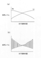
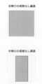
- the resolution related to the spatial frequency of this array is shown in Fig. 1 (bottom).
- the types of color filters and aperture masks are multiplexed on one sensor surface, when they are separated into specific colors of specific aperture masks and the critical resolution frequency is viewed, they are the Nyquist of the original pixel. It only has a resolution that never reaches the frequency.
- the final left-view color image is output to the original Nyquist frequency by superimposing the left-view image, which has only a small resolving power in the frequency space, and the intermediate image without parallax. can do.
- the color image of the right viewpoint is output to the original Nyquist frequency by superimposing the left-view image, which has only a small resolving power in the frequency space, and the intermediate image without parallax. can do.
- the color image of the right viewpoint is output to the original Nyquist frequency by superimposing the left-view image, which has only a small resolving power in the frequency space, and the intermediate image without parallax. can do.
- the color image of the right viewpoint is output to the original Nyquist frequency by superimposing the left-view image, which has only a small resolving power in the frequency space, and the intermediate image without parallax.
- the left parallax pixel is bright on the right side and dark on the left side of the image capturing the subject image.
- the right parallax pixel is brighter on the left side of the image and darker on the right side. That is, even if the subject image is the same, the right parallax pixel and the left parallax pixel are captured as images with completely different illuminance.
- a method for simultaneously solving the problem of illuminance mismatch between parallax pixels and the problem of subject position mismatch due to parallax based on the characteristics of the subject image of the monocular pupil division method. That is, as shown in FIG. 14, in the monocular pupil division imaging, the focused subject image does not cause a parallax shift in the left and right parallax pixels, and only the subject image at the out-of-focus position, A parallax shift occurs. That is, the parallax is included only in the blur. As shown in FIG. 3, the blurred subject image can generate an image without parallax by simply taking an average.
- the imaging signal is generated as it is without changing even if the parallax average between the left and right is taken, while at the position of the blurred subject image,
- the parallax average between the left and right disappears completely, and the problem of gain mismatch due to illuminance unevenness also disappears completely and can be solved simultaneously.
- arithmetic mean a subject image with a large blur width, which is the sum of the two blur widths, is generated at an intermediate position.
- geometric mean a subject image having the same blur width as the blur width divided into two is generated at the intermediate position.
- a subject image having the same blur width as that of the pixels with no parallax of the entire aperture is formed, and in the case of the geometric average, a subject image having the same blur width as that of the parallax pixels of the half aperture is formed.
- the intermediate image without parallax can be used as a conventional high-resolution two-dimensional image for monitor display and print output.
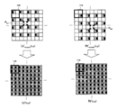
- a left parallax image and a right parallax image with low spatial frequency resolution are generated. Performs simple average interpolation in the G color plane, where only the left parallax pixels are collected. Linear interpolation is performed according to the ratio of distances using adjacent pixel values. Similarly, simple average interpolation in the G color plane in which only the right parallax pixels are collected is performed. That, Lt mosaic (x, y) Lt from (x, y) and, Rt mosaic (x, y) from the Rt (x, y) to produce a.
- Temporary left parallax image Lt (x, y)
- Temporary right parallax image Rt (x, y)
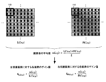
- step 4 Generation of parallax-free color mosaic image by correcting left and right illumination distribution (local gain balance correction)
- local gain correction is performed in units of pixels to match the illuminance of the left parallax pixel in the screen and the right parallax pixel in the screen.
- a new Bayer surface with gain matching is created. This is equivalent to replacing with an average value, and a Bayer surface in which the parallax disappears is created.
- M N x, y
- target value setting methods to be used as reference points for each pixel there are two types of target value setting methods to be used as reference points for each pixel: a method of selecting an arithmetic mean and a method of selecting a geometric mean.
- the process of applying local gain correction to each pixel is actually only necessary to substitute the average value of each pixel obtained first.
- the local gain correction is a modulation process for eliminating the parallax.
- an arithmetic average is employed. In this way, the Bayer plane data is rewritten using the average value of the left viewpoint image and the right viewpoint image as the non-parallax pixel value of the new G pixel position, and the Bayer plane image M N (x, y) without parallax is output. To do.
- the technology USP6,836,572 for increasing the resolution of the direction determination of the same inventor as the present applicant and resolving the vertical and horizontal Nyquist frequencies
- the technology USP7,236,628 for increasing the resolution in the oblique direction when calculating the interpolation value
- adaptive false color countermeasure technology USP7,391,903 by color gradient judgment method and technology to increase resolution of direction judgment The best high-performance demosaic technology used in is introduced.
- the positive offset value ⁇ is set to a larger value as the imaging condition with higher sensitivity increases the dark current noise component.
- step S4 the CPU performs an interpolation process as follows.
- a pixel having R component color information is referred to as an R pixel
- a pixel having B component color information is referred to as a B pixel
- a pixel having G component color information is referred to as a G pixel.
- the signal value of the R component corresponding to the pixel indicated by i, j] is R [i, j]
- the signal value of the G component is G [i, j]
- the signal value of the B component is B [i, j]. I will represent it.
- the CPU determines the vertical similarity CvN [i, j] and the horizontal similarity ChN [i, j] for the pixel (R pixel or B pixel) that is not the G pixel indicated by the pixel position [i, j].
- Z [i, j] is the signal value of the R component or B component indicated by the pixel position [i, j].
- the first term is the similarity between the same colors that represents the similarity between the same colors at two pixel intervals
- the second term is the similarity between the different colors that represents the similarity between the different colors at the adjacent pixel intervals.
- the similarity between different colors has the ability to resolve vertical and horizontal Nyquist frequencies.
- the absolute value of the first term in the above equations (3) and (4) is to detect rough directionality by comparing the G color components.
- the absolute values of the second and third terms in the above equations (3) and (4) detect fine similarities that cannot be detected by the first term.
- the CPU calculates the vertical similarity and the horizontal similarity obtained by the above formulas (3) and (4) for each coordinate, and calculates the vertical and horizontal similarity in the target coordinates [i, j]. Based on the following equation (5), the direction of similarity is determined.
- Th is a determination threshold value used to avoid erroneous determination due to noise included in the signal value, and is changed according to the ISO sensitivity.
- the CPU interpolates the G component using the unevenness information of the R component or the B component. That is, information on whether or not to interpolate to an external dividing point that cannot be predicted only by interpolation of the inner G component of the surrounding G component, information on the same color component that is located in the vicinity of information on other color components existing at the interpolation target position And determining whether the image structure is convex upward or downward. That is, the information of the high frequency component obtained by sampling other color components is superimposed on the interpolation target color component.
- the G color complement is calculated by the following formulas (6) and (9) when the vertical direction is similar to the position [i, j] of the center R pixel shown in FIG.
- Z [i, j] is the signal value of the R component or B component indicated by the pixel position [i, j].
- the first term in the above equation (9) is calculated from the G component signal values G [i, j-1] and G [i, j + 1] arranged vertically with respect to the pixel position [i, j]. Represents the average value.
- the second term in the above equation (9) is the amount of change calculated from the R component signal values R [i, j], R [i, j-2] and R [i, j + 2] arranged vertically. To express. By adding the amount of change in the R component signal value to the average value of the G component signal value, the G component interpolation value G [i, j] is obtained. Since such interpolation can be predicted except for the internal dividing point of the G component, it will be referred to as extrapolation for convenience.
- the above equation (10) performs extrapolation in the horizontal direction using the signal values of the pixels arranged horizontally with respect to the pixel position [i, j], as in the case of the extrapolation in the vertical direction described above. It is.
- the CPU calculates the G color interpolation values by the above formulas (9) and (10), and takes the average of the two calculated G color interpolation values. Let it be a G color interpolation value.
- R interpolation For R color interpolation, pixel positions [i + 1, j], [i, j + 1], [i + 1, j other than the R pixel position [i, j] shown in FIG. +1] is calculated by the following equations (11) to (13), respectively. At this time, unevenness information of G component signal values (FIG. 7 of WO2006 / 006373) corresponding to all pixel positions obtained by the G interpolation described above is used.
- the first term in the above equations (11) to (13) represents an average value calculated from the R component signal value adjacent to the coordinates to be subjected to R component interpolation, and the first term in the above equations (11) to (13).
- B interpolation For the B component interpolation, interpolation processing is performed in the same manner as the R component. For example, for pixel positions [i + 1, j], [i, j + 1], [i + 1, j + 1] other than the position [i, j] of the B pixel shown in FIG. 8 of WO2006 / 006373 Are calculated by the following equations (14) to (16), respectively. At this time, the unevenness information of the G component signal values (FIG. 9 of WO2006 / 006373) corresponding to all the pixel positions obtained by the G interpolation described above is used.
- the change amount of the G component signal value is added to the average value of the B component signal value to obtain the B component interpolation value.
- step 5-3 Transition to original linear gradation space by inverse gradation conversion
- the inverse gradation conversion of step 5-1 is performed on each Bayer-interpolated RGB color plane to return to linear gradation RGB data.
- the obtained RGB color image without parallax is represented by R N (x, y), G N (x, y), and B N (x, y). These are RGB data expressed in linear gradation.
- This can be called parallax modulation because the displacement processing is realized by superimposing the parallax components of the temporary parallax image.
- parallax modulation methods There are two types of parallax modulation methods: a method using an arithmetic average as a reference point and a method using a geometric average as a reference point. Both can obtain a parallax modulation effect, but when the aperture mask of pixels without parallax of the image sensor is full aperture, a method using an arithmetic average as a reference point is adopted, and the aperture mask of pixels without parallax is a pixel with parallax. It is better to adopt a method using the geometric mean as a reference point when the same half aperture is used. Therefore, in this embodiment, a method using an arithmetic mean as a reference point is used.
- step 6 the parallax modulation calculation formula defined in step 6 and the parallax extinction calculation formula (local gain balance correction) for correcting illuminance unevenness between the left and right defined in step 4 are just in inverse relationship. It can be seen that modulation is applied by multiplying. Therefore, in step 6, it works in the direction in which the parallax is applied, and in step 4, it works in the direction in which the parallax disappears.
- Effect 1 As a solution based on the characteristics peculiar to the monocular pupil division method, the effect of simultaneously eliminating the illuminance distribution mismatch between the left and right and the subject position mismatch due to the presence of parallax.
- the two problems of parallax shift and illuminance difference are matched, and there is no parallax Intermediate images can be generated.
- Effect 2 The assets of the conventional demosaic technology can be used as they are, and a high-resolution image can be generated.
- the non-parallax pixel has a blur width at the time of the full opening that is the sum of the opening areas of the left parallax pixel and the right parallax pixel.
- a measure was taken to match the blur width of the captured subject image of the non-parallax pixels by taking the arithmetic mean of the left and right parallax pixel values.
- the color image without parallax forms a subject image that matches the blur width of the entire aperture, so the left and right viewpoint images are used as the denominator of the parallax modulation that keeps the ratio constant.
- An image having the blur width of the full aperture by the arithmetic average of the above is taken as a reference point, and the left and right color images after parallax modulation are modulated again so as to become an image having the blur width of the half aperture.
- Embodiments 1 to 3 has the same shape as the left parallax pixel and the right parallax pixel, and an aperture mask having the same aperture area is arranged at the center of the pixel, there is no parallax in the pixel with parallax.
- a measure is taken to use the geometric average as the average value of the left and right parallax pixel values to match the blur width of the captured subject image of the non-parallax pixel.
- the color image without parallax forms a subject image that matches the half-openness blur width, so the left and right viewpoint images are used as the denominator of the parallax modulation that keeps the ratio constant.
- An image having a half-aperture blur width based on the geometric average is taken as a reference point, and the left and right color images after parallax modulation are again modulated so as to become an image having a half-aperture blur width.
- both the parallax extinction process for correcting illuminance unevenness and the process of adding parallax modulation at the end are all performed using the arithmetic mean as a reference point. It is good.
- the non-parallax pixel has a half-aperture mask area
- the calculation is performed using the geometric mean as a reference point in both the parallax extinction process for correcting illuminance unevenness and the final parallax modulation process. It is good.
- Flow chart the same as in the first embodiment.
- R N_mosaic (x, y) R Lt_mosaic (x, y), the signal surface of the left parallax pixel of R component, R Rt_mosaic (x, y), the signal surface of the right parallax pixel of the R component, G N_mosaic (x, y), the signal plane of the left parallax pixel of G component, G Lt_mosaic (x, y) G Rt_mosaic (x, y), the signal plane of the right parallax pixel of G component, B N_mosaic (x, y)
- B Lt_mosaic (x, y) be the signal surface of the left parallax pixel of the B component, B Rt_mosaic (x, y) It will be expressed as
- a temporary left parallax image and a temporary right parallax image with low spatial frequency resolution are generated. Performs simple average interpolation in the G color plane, where only the left parallax pixels are collected. Linear interpolation is performed according to the distance ratio using pixel values that are close to each other. Similarly, simple average interpolation in the G color plane in which only the right parallax pixels are collected is performed. Similarly, simple average interpolation in the G color plane in which only non-parallax pixels are collected is performed. Similar processing is performed for each of R, G, and B.
- Temporary R component-free parallax image R N (x, y) Temporary G component parallax-free image: G N (x, y) Temporary B component non-parallax image: B N (x, y) Temporary R component left parallax image: R Lt (x, y) Temporary G component left parallax image: G Lt (x, y) Temporary B component left parallax image: B Lt (x, y) Temporary R component right parallax image: R Rt (x, y) Temporary G component right parallax image: G Rt (x, y) Temporary B component right parallax image: B Rt (x, y) When creating temporary non-parallax images R N (x, y), G N (x, y), and B N (x, y), high-definition is performed by introducing direction determination in the signal plane. May be.
- the Bayer plane data is rewritten by using the pixel value obtained by averaging the average value of the left viewpoint image and the right viewpoint image with the reference viewpoint image having no parallax as a new non-parallax pixel value. None Outputs the Bayer plane image M N (x, y).
- the provisional right parallax color images R Rt (x, y), G Rt (x, y), B Rt (x, y) generated in step 3 and intermediate processing in step 5 are generated.
- color image R N without high resolution parallax (x, y), G N (x, y), using B N (x, y), color image actually output to high right parallax resolving power R 'Rt (x, y), G ′ Rt (x, y), and B ′ Rt (x, y) are generated.
- parallax modulation methods There are two types of parallax modulation methods: a method using an arithmetic average as a reference point and a method using a geometric average as a reference point. Both can obtain a parallax modulation effect, but when the aperture mask of pixels without parallax of the image sensor is full aperture, a method using an arithmetic average as a reference point is adopted, and the aperture mask of pixels without parallax is a pixel with parallax. A method using the geometric mean as the reference point for the same half aperture is adopted. Therefore, in this embodiment, a method using an arithmetic mean as a reference point is used.
- a temporary left parallax image and a temporary right parallax image with low spatial frequency resolution are generated.
- Simple average interpolation is performed in the signal plane that collects only the left parallax pixels. Linear interpolation is performed according to the distance ratio using pixel values that are close to each other. Similarly, simple average interpolation is performed in the signal plane in which only the right parallax pixels are collected. Similarly, simple average interpolation is performed in the signal plane in which only non-parallax pixels are collected.
- parallax modulation methods There are two types of parallax modulation methods: a method using an arithmetic average as a reference point and a method using a geometric average as a reference point. Both can obtain a parallax modulation effect, but when the aperture mask of pixels without parallax of the image sensor is full aperture, a method using an arithmetic average as a reference point is adopted, and the aperture mask of pixels without parallax is a pixel with parallax. A method using the geometric mean as the reference point for the same half aperture is adopted. Therefore, in this embodiment, a method using an arithmetic mean as a reference point is used.
- an image obtained by performing conventional Bayer interpolation is generated as an intermediate image, and a parallax image having a low resolution obtained from each of R, G, and B is used to perform parallax modulation using the same method as in the second embodiment.
- a high-resolution left parallax color image and a right parallax color image can be created. In this way, it is possible to cope with the uneven illuminance problem between the left and right parallax pixels that occurs in the conventional image sensor.
- the left and right parallax pixels have been described. However, even if these image sensors are rotated 90 ° to obtain a vertical parallax, the uneven illuminance correction is performed in exactly the same manner. be able to. The same applies to an image sensor that rotates 45 ° and has an oblique parallax.
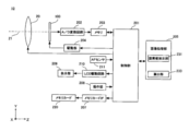
- FIG. 7 is a diagram illustrating the configuration of the digital camera 10.
- the digital camera 10 includes a photographic lens 20 as a photographic optical system, and guides a subject light beam incident along the optical axis 21 to the image sensor 100.
- the photographing lens 20 may be an interchangeable lens that can be attached to and detached from the digital camera 10.
- the digital camera 10 includes an image sensor 100, a control unit 201, an A / D conversion circuit 202, a memory 203, a drive unit 204, an image processing unit 205, a memory card IF 207, an operation unit 208, a display unit 209, an LCD drive circuit 210, and an AF.
- a sensor 211 is provided.
- the direction parallel to the optical axis 21 toward the image sensor 100 is defined as the Z-axis plus direction
- the direction toward the front of the drawing on the plane orthogonal to the Z-axis is the X-axis plus direction
- the upward direction on the drawing is Y.
- the axis is defined as the plus direction.
- the coordinate axes are displayed so that the orientation of each figure can be understood with reference to the coordinate axes in FIG.
- the photographing lens 20 is composed of a plurality of optical lens groups, and forms an image of a subject light flux from the scene in the vicinity of its focal plane.
- the photographic lens 20 is represented by a single virtual lens arranged in the vicinity of the pupil.
- the image sensor 100 is disposed near the focal plane of the photographic lens 20.
- the image sensor 100 is an image sensor such as a CCD or CMOS sensor in which a plurality of photoelectric conversion elements are two-dimensionally arranged.
- the image sensor 100 is controlled in timing by the drive unit 204, converts the subject image formed on the light receiving surface into an image signal, and outputs the image signal to the A / D conversion circuit 202.
- the A / D conversion circuit 202 converts the image signal output from the image sensor 100 into a digital image signal and outputs the digital image signal to the memory 203.
- the image processing unit 205 performs various image processing using the memory 203 as a work space, and generates image data. In particular, the image processing unit 205 extracts a pixel value from the target pixel position of the color image data and the parallax image data, and extracts a pixel value as color image data at the target pixel position using the extracted pixel value.
- a calculation unit 233 for calculating is provided. Details of each processing will be described later.
- the image processing unit 205 also has general image processing functions such as adjusting image data according to the selected image format.
- the generated image data is converted into a display signal by the LCD drive circuit 210 and displayed on the display unit 209.
- the data is recorded on the memory card 220 attached to the memory card IF 207.
- the AF sensor 211 is a phase difference sensor in which a plurality of distance measuring points are set with respect to the subject space, and detects the defocus amount of the subject image at each distance measuring point.
- a series of shooting sequences is started when the operation unit 208 receives a user operation and outputs an operation signal to the control unit 201.
- Various operations such as AF and AE accompanying the imaging sequence are executed under the control of the control unit 201.
- the control unit 201 analyzes the detection signal of the AF sensor 211 and executes focus control for moving a focus lens that constitutes a part of the photographing lens 20.
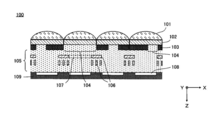
- FIG. 8 is a schematic diagram illustrating a cross section of the image sensor 100.
- the imaging element 100 is configured by arranging a micro lens 101, a color filter 102, an aperture mask 103, a wiring layer 105, and a photoelectric conversion element 108 in order from the subject side.
- the photoelectric conversion element 108 is configured by a photodiode that converts incident light into an electrical signal.
- a plurality of photoelectric conversion elements 108 are two-dimensionally arranged on the surface of the substrate 109.
- the image signal converted by the photoelectric conversion element 108, the control signal for controlling the photoelectric conversion element 108, and the like are transmitted / received via the wiring 106 provided in the wiring layer 105.
- an opening mask 103 having openings 104 provided in one-to-one correspondence with each photoelectric conversion element 108 is provided in contact with the wiring layer.
- the opening 104 is shifted for each corresponding photoelectric conversion element 108 so that the relative position is precisely determined.
- parallax occurs in the subject light beam received by the photoelectric conversion element 108 by the action of the opening mask 103 including the opening 104.
- the aperture mask 103 does not exist on the photoelectric conversion element 108 that does not generate parallax.
- an aperture mask 103 having an aperture 104 that does not limit the subject luminous flux incident on the corresponding photoelectric conversion element 108, that is, allows the entire incident luminous flux to pass therethrough is provided.
- the aperture 107 formed by the wiring 106 defines the incident light flux that is incident, so the wiring 106 is regarded as an aperture mask that allows the entire incident light flux that does not cause parallax to pass.
- the opening mask 103 may be arranged separately and independently corresponding to each photoelectric conversion element 108, or may be formed collectively for a plurality of photoelectric conversion elements 108 in the same manner as the manufacturing process of the color filter 102. .
- the color filter 102 is provided on the opening mask 103.
- the color filter 102 is a filter provided in a one-to-one correspondence with each photoelectric conversion element 108, which is colored so as to transmit a specific wavelength band to each photoelectric conversion element 108.
- the microlens 101 is provided on the color filter 102.
- the microlens 101 is a condensing lens for guiding more incident subject light flux to the photoelectric conversion element 108.
- the microlenses 101 are provided in a one-to-one correspondence with the photoelectric conversion elements 108.
- the optical axis of the microlens 101 is shifted so that more subject light flux is guided to the photoelectric conversion element 108. It is preferable.
- the arrangement position may be adjusted so that more specific subject light beam, which will be described later, is incident along with the position of the opening 104 of the opening mask 103.
- one unit of the aperture mask 103, the color filter 102, and the microlens 101 provided on a one-to-one basis corresponding to each photoelectric conversion element 108 is referred to as a pixel.
- a pixel provided with the opening mask 103 that generates parallax is referred to as a parallax pixel
- a pixel that is not provided with the opening mask 103 that generates parallax is referred to as a non-parallax pixel.
- the effective pixel area of the image sensor 100 is about 24 mm ⁇ 16 mm, the number of pixels reaches about 12 million.
- the microlens 101 may not be provided.
- the wiring layer 105 is provided on the side opposite to the photoelectric conversion element 108. Further, if the opening 104 of the opening mask 103 has a color component, the color filter 102 and the opening mask 103 can be formed integrally.
- the opening mask 103 and the wiring 106 are provided as separate bodies, but the wiring 106 may be responsible for the function of the opening mask 103 in the parallax pixels. That is, a prescribed opening shape is formed by the wiring 106, and the incident light beam is limited by the opening shape to guide only a specific partial light beam to the photoelectric conversion element 108. In this case, the wiring 106 that forms the opening shape is preferably closest to the photoelectric conversion element 108 in the wiring layer 105.
- the opening mask 103 may be formed by a permeation blocking film provided to overlap the photoelectric conversion element 108.
- the opening mask 103 is formed, for example, by sequentially laminating a SiN film and a SiO 2 film to form a permeation blocking film and removing a region corresponding to the opening 104 by etching.
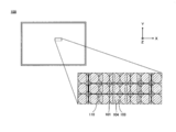
- FIG. 9 is a schematic diagram illustrating a state in which a part of the image sensor 100 is enlarged.
- the color arrangement of the color filter 102 is not considered until the reference is resumed later.
- the repetitive pattern described below may be considered as an adjacent pixel in the color filter 102 of the same color.
- the opening 104 of the opening mask 103 is provided with a relative shift with respect to each pixel.
- the openings 104 are provided at positions displaced from each other.
- the entire image sensor 100 has a two-dimensional and periodic array of photoelectric conversion element groups each including a set of six parallax pixels each having an aperture mask 103 that gradually shifts from the left side to the right side of the drawing. .
- FIG. 10 is a conceptual diagram illustrating the relationship between the parallax pixels and the subject.
- FIG. 10A shows a photoelectric conversion element group of a repetitive pattern 110t arranged at the center orthogonal to the photographing optical axis 21 in the image pickup element 100
- FIG. 10B shows a repetitive arrangement arranged in the peripheral portion.
- the photoelectric conversion element group of the pattern 110u is typically shown.
- the subject 30 in FIGS. 10A and 10B is in the in-focus position with respect to the photographic lens 20.
- FIG. 10C schematically shows the relationship when the subject 31 existing at the out-of-focus position with respect to the photographing lens 20 is captured corresponding to FIG.
- the subject luminous flux passes through the pupil of the photographic lens 20 and is guided to the image sensor 100.
- Six partial areas Pa to Pf are defined for the entire cross-sectional area through which the subject luminous flux passes. For example, in the pixel at the left end of the sheet of the photoelectric conversion element group constituting the repetitive patterns 110t and 110u, only the subject luminous flux emitted from the partial region Pf reaches the photoelectric conversion element 108 as can be seen from the enlarged view.
- the position of the opening 104f of the opening mask 103 is determined.
- the position of the opening 104e corresponding to the partial area Pe the position of the opening 104d corresponding to the partial area Pd, and the position of the opening 104c corresponding to the partial area Pc.
- the position of the opening 104b is determined corresponding to the partial area Pb
- the position of the opening 104a is determined corresponding to the partial area Pa.
- the position of the opening 104f is determined by the inclination of the principal ray Rf of the subject light beam (partial light beam) emitted from the partial region Pf, which is defined by the relative positional relationship between the partial region Pf and the leftmost pixel, for example. It may be said that it is established. Then, when the photoelectric conversion element 108 receives the subject luminous flux from the subject 30 existing at the in-focus position via the opening 104f, the subject luminous flux is coupled on the photoelectric conversion element 108 as shown by the dotted line. Image.
- the position of the opening 104e is determined by the inclination of the principal ray Re
- the position of the opening 104d is determined by the inclination of the principal ray Rd
- the position of the opening 104c is determined by the inclination of the principal ray Rc.
- the position of the opening 104b is determined by the inclination of the light ray Rb
- the position of the opening 104a is determined by the inclination of the principal ray Ra.
- the light beam emitted from the minute region Ot on the subject 30 that intersects the optical axis 21 among the subject 30 existing at the in-focus position passes through the pupil of the photographing lens 20.
- each pixel of the photoelectric conversion element group constituting the repetitive pattern 110t is reached. That is, each pixel of the photoelectric conversion element group constituting the repetitive pattern 110t receives the light beam emitted from one minute region Ot through the six partial regions Pa to Pf.
- the minute region Ot has an extent corresponding to the positional deviation of each pixel of the photoelectric conversion element group constituting the repetitive pattern 110t, it can be approximated to substantially the same object point.
- the luminous flux emitted from the minute region Ou on the subject 30 that is separated from the optical axis 21 among the subject 30 that exists at the in-focus position is reflected on the pupil of the photographing lens 20. It passes through and reaches each pixel of the photoelectric conversion element group constituting the repetitive pattern 110u. That is, each pixel of the photoelectric conversion element group constituting the repetitive pattern 110u receives a light beam emitted from one minute region Ou via each of the six partial regions Pa to Pf.
- the micro area Ou has an extent corresponding to the positional deviation of each pixel of the photoelectric conversion element group constituting the repetitive pattern 110u, but substantially the same object point. Can be approximated.
- the minute area captured by the photoelectric conversion element group differs according to the position of the repetitive pattern 110 on the image sensor 100, and each pixel constituting the photoelectric conversion element group Captures the same minute region through different partial regions.
- each repetitive pattern 110 corresponding pixels receive the subject luminous flux from the same partial area. That is, in the drawing, for example, the leftmost pixel of each of the repeated patterns 110t and 110u receives a partial light beam from the same partial region Pf.
- each of the parallax pixels arranged on the image sensor 100 includes one of six types of aperture masks.
- the subject luminous flux from the subject 31 present at the out-of-focus position passes through the six partial areas Pa to Pf of the pupil of the photographing lens 20 and reaches the image sensor 100.
- the subject light flux from the subject 31 existing at the out-of-focus position forms an image at another position, not on the photoelectric conversion element 108.
- the subject luminous flux forms an image on the subject 31 side with respect to the photoelectric conversion element 108.
- the subject luminous flux forms an image on the opposite side of the subject 31 from the photoelectric conversion element 108.
- the subject luminous flux radiated from the minute region Ot ′ among the subjects 31 existing at the out-of-focus position depends on which of the six partial regions Pa to Pf, the corresponding pixels in different sets of repetitive patterns 110.
- the subject luminous flux that has passed through the partial region Pd is incident on the photoelectric conversion element 108 having the opening 104d included in the repeated pattern 110t ′ as the principal ray Rd ′.
- the subject light beam that has passed through another partial region does not enter the photoelectric conversion element 108 included in the repetitive pattern 110t ′, and the repetitive pattern in the other repetitive pattern.
- the subject luminous flux reaching each photoelectric conversion element 108 constituting the repetitive pattern 110t ′ is a subject luminous flux radiated from different minute areas of the subject 31. That is, a subject luminous flux having a principal ray as Rd ′ is incident on 108 corresponding to the opening 104d, and the principal rays are incident on Ra + , Rb + , Rc + , Re to the photoelectric conversion elements 108 corresponding to the other openings. +, although subject light flux to Rf + is incident, these object light is a subject light flux emitted from different micro region of the object 31. Such a relationship is the same in the repeated pattern 110u arranged in the peripheral portion in FIG.
- the subject image A captured by the photoelectric conversion element 108 corresponding to the opening 104a and the subject image D captured by the photoelectric conversion element 108 corresponding to the opening 104d are: If the image is for the subject present at the in-focus position, there is no shift, and if the image is for the subject present at the out-of-focus position, there is a shift. Then, the direction and amount of the shift are determined by how much the subject existing at the out-of-focus position is shifted from the focus position and by the distance between the partial area Pa and the partial area Pd. That is, the subject image A and the subject image D are parallax images. Since this relationship is the same for the other openings, six parallax images are formed corresponding to the openings 104a to 104f.
- a parallax image is obtained by gathering together the outputs of pixels corresponding to each other in each of the repetitive patterns 110 configured as described above. That is, the output of the pixel that has received the subject light beam emitted from a specific partial area among the six partial areas Pa to Pf forms a parallax image.
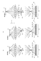
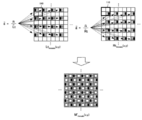
- FIG. 11 is a conceptual diagram illustrating processing for generating a parallax image.
- the figure shows, in order from the left column, the generation of the parallax image data Im_f generated by collecting the outputs of the parallax pixels corresponding to the opening 104f, the generation of the parallax image data Im_e by the output of the opening 104e, the opening State of generation of parallax image data Im_d by output of 104d, state of generation of parallax image data Im_c by output of opening 104c, state of generation of parallax image data Im_b by output of opening 104b, parallax by output of opening 104a
- the parallax image data Im_f is generated by the output of the opening 104f will be described.
- the repetitive pattern 110 composed of a group of photoelectric conversion elements including a set of six parallax pixels is arranged in a horizontal row. Therefore, the parallax pixels having the opening 104f are present every six pixels in the left-right direction and continuously in the vertical direction on the virtual imaging element 100 excluding the pixels without parallax. Each of these pixels receives the subject luminous flux from different microregions as described above. Therefore, when the outputs of these parallax pixels are collected and arranged, a parallax image is obtained.
- each pixel of the image sensor 100 according to the present embodiment is a square pixel, simply gathering results in the result that the number of pixels in the horizontal direction is reduced to 1/6, and vertically long image data is generated. End up. Therefore, by performing an interpolation process to obtain the number of pixels 6 times in the horizontal direction, the parallax image data Im_f is generated as an image with an original aspect ratio.
- the parallax image data before the interpolation processing is an image that is thinned by 1/6 in the horizontal direction, the resolution in the horizontal direction is lower than the resolution in the vertical direction. That is, it can be said that the number of generated parallax image data and the improvement in resolution are in a conflicting relationship.
- a specific interpolation process applied to this embodiment will be described later.
- parallax image data Im_e to parallax image data Im_a are obtained. That is, the digital camera 10 can generate a six-view parallax image having parallax in the horizontal direction.
- Im_af is image data obtained by calculating an arithmetic average between Im_f and Im_a in order to eliminate parallax.
- an arithmetic mean between Im_e and Im_b is taken as Im_be.
- Im_cd an arithmetic average between Im_d and Im_c.
- Im_cd an arithmetic average between Im_d and Im_c.
- the output image Im_out thus obtained is a 2D image without parallax from which the influence of the illuminance difference has been removed, and a wide blur width obtained by combining all the blur widths over 6 parallaxes, that is, a pixel with no parallax having a full aperture mask An image of the subject with the same blur width is obtained.
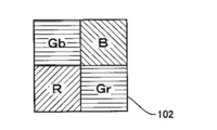
- FIG. 12 is a diagram for explaining the Bayer arrangement.
- the Bayer array is an array in which the green filter is assigned to the upper left and lower right pixels, the red filter is assigned to the lower left pixel, and the blue filter is assigned to the upper right pixel.
- the upper left pixel to which the green filter is assigned is the Gb pixel
- the lower right pixel to which the green filter is assigned is the Gr pixel.
- a pixel to which a red filter is assigned is an R pixel
- a pixel to which blue is assigned is a B pixel.
- a horizontal direction in which Gb pixels and B pixels are arranged is defined as Gb row, and a horizontal direction in which R pixels and Gr pixels are arranged is defined as Gr row.
- a vertical direction in which Gb pixels and R pixels are arranged is a Gb column, and a vertical direction in which B pixels and Gr pixels are arranged is a Gr column.
- a huge number of repetitive patterns 110 can be set for such an array of the color filters 102 depending on what color pixels the parallax pixels and non-parallax pixels are allocated to. For example, if many non-parallax pixels are allocated, high-resolution 2D image data is obtained, and if all pixels of RGB are equally allocated, high-quality 2D image data with little color shift is obtained. . However, in this case, since the number of parallax pixels is relatively small, the image quality is degraded as a 3D image including a plurality of parallax images.
- a repetitive pattern 110 having various characteristics is set depending on which pixel is a parallax pixel or a non-parallax pixel.
- each of the parallax pixels is a parallax Lt pixel that is eccentric to the left side of the opening 104 and a parallax Rt pixel that is also eccentric to the right side.
- the two viewpoint parallax images output from such parallax pixels realize so-called stereoscopic vision.
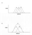
- FIG. 13 is a diagram for explaining the concept of defocusing in a pixel without parallax.
- FIG. 13A when an object point that is a subject exists at the focal position, the subject luminous flux that reaches the image sensor light receiving surface through the lens pupil is steep with the pixel at the corresponding image point as the center. The light intensity distribution is shown.
- the subject luminous flux exhibits a gentle light intensity distribution on the light receiving surface of the image sensor as compared with the case where the object point exists at the focal position. . That is, the output value at the pixel of the corresponding image point is lowered, and a distribution having output values up to the peripheral pixels is shown.
- the subject luminous flux when the object point further deviates from the focal position, the subject luminous flux exhibits a gentler light intensity distribution on the image sensor light receiving surface.
- the output value at the pixel of the corresponding image point further decreases, and a distribution having output values up to the surrounding pixels is shown.
- FIG. 14 is a diagram for explaining the concept of defocusing in a parallax pixel.
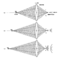
- the parallax Lt pixel and the parallax Rt pixel receive the subject luminous flux that arrives from one of the two parallax virtual pupils set as the optical axis target as a partial region of the lens pupil.
- the peak of the light intensity distribution indicated by the parallax Lt pixel corresponds to the image point, compared to the case where the object point exists at the focal position. Appearing at a position away from the pixel in one direction, and its output value decreases. In addition, the width of the pixel having the output value is increased. The peak of the light intensity distribution indicated by the parallax Rt pixel appears at a position away from the pixel corresponding to the image point in the opposite direction to the one direction in the parallax Lt pixel and at an equal distance, and the output value similarly decreases. Similarly, the width of the pixel having the output value is increased.
- the same light intensity distribution that is gentler than that in the case where the object point exists at the focal position appears at an equal distance from each other. Further, as shown in FIG. 14C, when the object point is further deviated from the focal position, the same light intensity distribution that is more gentle than the state of FIG. 14B appears further apart. . That is, it can be said that the amount of blur and the amount of parallax increase as the object point deviates from the focal position.
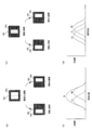
- FIG. 13 is a graph showing the change in the light intensity distribution described in FIG. 13 and the change in the light intensity distribution described in FIG.
- the horizontal axis represents the pixel position, and the center position is the pixel position corresponding to the image point.
- the vertical axis represents the output value of each pixel. Since this output value is substantially proportional to the light intensity, it is shown as the light intensity in the figure.
- FIG. 15A is a graph showing changes in the light intensity distribution described in FIG.
- a distribution curve 1801 represents the light intensity distribution corresponding to FIG. 13A and shows the steepest state.
- a distribution curve 1802 represents a light intensity distribution corresponding to FIG. 13B, and a distribution curve 1803 represents a light intensity distribution corresponding to FIG.
- the peak value gradually decreases and has a broadening.
- FIG. 15B is a graph showing changes in the light intensity distribution described in FIG.
- a distribution curve 1804 and a distribution curve 1805 represent the light intensity distribution of the parallax Lt pixel and the light intensity distribution of the parallax Rt pixel in FIG. As can be seen from the figure, these distributions have a line-symmetric shape with respect to the center position. Further, a combined distribution curve 1806 obtained by adding them shows a similar shape to the distribution curve 1802 in FIG. 13B, which is in the same defocused state as in FIG. 14B.
- the distribution curve 1807 and the distribution curve 1808 represent the light intensity distribution of the parallax Lt pixel and the light intensity distribution of the parallax Rt pixel in FIG. As can be seen from the figure, these distributions are also symmetrical with respect to the center position. Further, a combined distribution curve 1809 obtained by adding them shows a similar shape to the distribution curve 1803 in FIG. 13C, which is in the same defocused state as in FIG. 14C.
- FIG. 16 is a diagram illustrating the opening shape of the opening 104 when there are two types of parallax pixels.
- the shape of the opening 104l of the parallax Lt pixel and the shape of the opening 104r of the parallax Rt pixel are obtained by dividing the shape of the opening 104n of the non-parallax pixel by the center line 322, respectively.
- the example which is the same is shown. That is, in FIG. 16A, the area of the opening 104n of the non-parallax pixel is the sum of the area of the opening 104l of the parallax Lt pixel and the area of the opening 104r of the parallax Rt pixel.
- the opening 104n of the non-parallax pixel is referred to as a full-opening opening, and the opening 104l and the opening 104r are referred to as half-opening openings.
- the opening is directed to the reference direction.
- the opening 104l of the parallax Lt pixel and the opening 104r of the parallax Rt pixel are displaced in opposite directions with respect to a virtual center line 322 passing through the center (pixel center) of the corresponding photoelectric conversion element 108. Yes.
- the opening 104l of the parallax Lt pixel and the opening 104r of the parallax Rt pixel each generate parallax in one direction with respect to the reference direction and in the other direction opposite to the one direction.
- FIG. 16B shows the light intensity distribution when the object point is deviated from the focal position in the pixel having each opening shown in FIG.
- the curve Lt corresponds to the distribution curve 1804 in FIG. 15B
- the curve Rt corresponds to the distribution curve 1805 in FIG.
- a curve N corresponds to a pixel without parallax, and shows a similar shape to the combined distribution curve 1806 in FIG.
- Each of the openings 104n, 104l, and 104r has an aperture stop function. Therefore, the blur width of the non-parallax pixel having the opening 104n having an area double the opening 104l (opening 104r) is the Lt pixel and the parallax Rt pixel indicated by the combined distribution curve 1806 in FIG. It is about the same as the blur width of the added curve.
- FIG. 16C shows an example in which the shape of the opening 104l of the parallax Lt pixel, the shape of the opening 104r of the parallax Rt pixel, and the shape of the opening 104c of the parallax C pixel are all the same shape.
- the parallax C pixel is a pixel having no eccentricity.
- the parallax C pixel is a parallax pixel that outputs a parallax image, in that only the subject luminous flux having the central portion of the pupil as a partial region is guided to the photoelectric conversion element 108.
- a pixel having an opening corresponding to the reference direction is defined as a non-parallax pixel.
- the parallax C pixel in FIG. 16C having an opening at the center of the photoelectric conversion element is the non-parallax pixel as in the non-parallax pixel in FIG.
- the opening 104l, the opening 104r, and the opening 104c are half the area of the opening 104n illustrated in FIG.
- each of the openings 104 l and 104 r is in contact with a virtual center line 322 that passes through the center (pixel center) of the photoelectric conversion element 108.
- FIG. 16D shows the light intensity distribution when the object point is deviated from the focal position in the pixel having each opening shown in FIG.
- the curve Lt corresponds to the distribution curve 1804 in FIG. 15B
- the curve Rt corresponds to the distribution curve 1805 in FIG.
- Each of the openings 104c, 104l, and 104r has a function of an aperture stop. Therefore, the blur width of the parallax C pixel having the opening 104c having the same shape and the same area as the opening 104l and the opening 104r is approximately the same as the blur width of the parallax Lt pixel and the parallax Rt pixel.
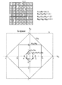
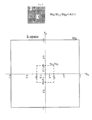
- FIG. 17 is a diagram illustrating an example of the repeating pattern 110 when there are two types of parallax pixels.
- the coordinate system of the digital camera 10 is defined by the X axis, the Y axis, and the Z axis.
- the x axis is defined in the right direction and the y axis is defined in the lower direction with reference to the left and upper end pixels. .
- the same four pixels as the Bayer array are used as the repeated pattern 110.
- the effective pixel area of the image sensor 100 is periodically arranged in the vertical and horizontal directions. In other words, the imaging device 100 uses a repetitive pattern 110 indicated by a thick line in the drawing as a basic lattice.
- the R pixel and the B pixel are non-parallax pixels, and the Gb pixel is assigned to the parallax L pixel and the Gr pixel is assigned to the parallax R pixel.
- the opening 104 is defined so that the parallax Lt pixel and the parallax Rt pixel included in the same repetitive pattern 110 receive the light beam emitted from the same minute region when the subject is in the in-focus position. .
- the non-parallax pixel is the opening portion of the full opening
- the parallax Lt pixel and the parallax Rt pixel are the opening portions of the half opening.
- the pixel pitch is a.
- the Gb pixel and the Gr pixel which are green pixels having high visibility, are used as the parallax pixels, it is expected to obtain a parallax image with high contrast.
- the Gb pixel and the Gr pixel which are the same green pixels are used as the parallax pixels, it is easy to perform a conversion operation from these two outputs to an output having no parallax, and the output of the R pixel and the B pixel which are non-parallax pixels is high. High-quality 2D image data can be generated.
- the left side is used as a virtual output of the parallax Lt pixel and the parallax Rt pixel that do not actually exist as the pixels of the image sensor 100 and have any of RGB color filters.
- the color image data of the viewpoint and the right viewpoint is acquired by a relatively simple process by a conversion operation.
- FIG. 1 (bottom) is a diagram showing the resolution related to the spatial frequency of an image captured by an image sensor employing the repetitive pattern 110 shown in FIG.
- f shows a frequency.
- the frequency resolution region is described by a first Brillouin zone representing a unit cell (Wigner-Zeilz cell) in a reciprocal lattice space.
- k y [ ⁇ ⁇ / a, + ⁇ / a] in the range of resolution. That is, the range surrounded by the dotted line is the limit resolution frequency of the image.
- the color filter and the aperture mask are arranged so as to overlap one sensor surface. Since the information captured by one sensor surface is constant, the amount of information is reduced by dividing the functions.
- the number of pixels without parallax is relatively reduced, and thus the amount of information obtained by the pixels without parallax is reduced.
- the color filter and the amount of individual information is reduced by the amount of R, G, B.
- the limit resolution frequency of the image does not reach the inherent Nyquist frequency.
- Image G Rt of the G component of the right-side perspective, the image R N of the R component of no parallax intermediate viewpoint, the image B N of the B component of intermediate viewpoint no disparity is the same.
- the image processing unit 205 performs processing for increasing the resolution in order to compensate for the amount of information reduced by dividing the functions.
- the G Lt pixel and G Rt pixel is parallax pixels, by replacing a virtual parallax without pixel G N, to produce a Bayer array of no parallax pixels only.
- an original Nyquist frequency k x [ ⁇ ⁇ / a, + ⁇ / a]
- k y [ ⁇ ⁇ / a, + ⁇ / a) as an intermediate image without parallax. ] Can be generated.
- each pixel in the pixel array shown in FIG. 17 includes various parallax pixels and non-parallax pixels when focusing on the opening 104, and various R pixels, G pixels, and B pixels when focusing on the color filter 102. Characterized in combination. Therefore, even if the outputs of the image sensor 100 are aligned with the pixel arrangement, they are not image data representing a specific image. That is, only when the pixel outputs of the image sensor 100 are separated and collected for each pixel group characterized by the same, image data representing one image corresponding to the feature is formed. For example, as already described with reference to FIG.
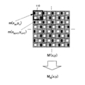
- the image processing unit 205 receives mosaic image data M mosaic (x, y), which is raw image data in which output values are arranged in the order of pixel arrangement of the image sensor 100.
- M mosaic x, y
- an image lacking at least one of R, G, and B information in each pixel is referred to as a mosaic image
- data forming the mosaic image is referred to as mosaic image data.
- At least one piece of information of R, G, and B is missing in each pixel, if it is not handled as an image in the first place, for example, if image data is composed of pixel values of monochrome pixels, it is treated as a mosaic image. Absent.
- Each output value is a linear gradation value proportional to the amount of light received by each photoelectric conversion element of the image sensor 100.
- the image processing unit 205 performs gain correction for matching the overall brightness between the left and right at this stage.
- the illuminance of light incident on the left parallax pixel and the illuminance of light incident on the right parallax pixel have a large difference not only in the relative distribution between the left and right but also in the average signal level of the entire image. This is because it occurs.
- the gain correction for matching the overall brightness between the left and right is called global gain correction.
- FIG. 18 is a diagram for explaining the calculation of the gain value.
- the mosaic image data of the left parallax pixel of the G component is Lt mosaic (x, y)
- the mosaic image data of the right parallax pixel of the G component is Rt mosaic ( x, y)
- FIG. 18 only the left and right parallax pixels are extracted and illustrated.
- the pixel types are described so that the types of pixels can be understood in accordance with the example of FIG. 17, but output values corresponding to the respective pixels are actually arranged.
- FIG. 19 is a diagram for explaining gain correction.
- the calculation unit 233 of the image processing unit 205 calculates the Lt mosaic (x, y) and Rt mosaic (x, y) pixels as illustrated.
- Gain correction is performed using the gain value. Specifically, gain correction for the left parallax pixel is performed by the following (Equation 1), and gain correction for the right parallax pixel is performed by (Equation 2).
- the mosaic image data M ′ mosaic (x, y) the mosaic image data of the G component left parallax pixel is the Lt ′ mosaic (x, y), the mosaic image data of the G component right parallax pixel.
- the calculation unit 233 of the image processing unit 205 performs mosaic image data M ′ mosaic in which the left parallax pixel and the right parallax pixel in M mosaic (x, y) are each corrected with one gain coefficient, as illustrated. (X, y) can be generated.
- the image processing unit 205 generates a left parallax image and a right parallax image with low spatial frequency resolution as temporary parallax images.
- FIG. 20 is a diagram for explaining generation of a temporary parallax image.
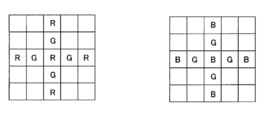
- the image processing unit 205 separates the mosaic image data M ′ mosaic (x, y) into a plurality of plane data. Each plane data at this point has an output value only at a pixel position where the output value exists in the RAW original image data. Therefore, the image processing unit 205 performs an interpolation process based on each plane data, and generates plane data in which vacancies are filled.
- the left side of the upper diagram shows Lt ′ mosaic (x, y), which is plain data obtained by extracting only the left parallax pixels from the mosaic image data M ′ mosaic (x, y), and the right side shows the right parallax.
- Lt ′ mosaic (x, y) which is plain data obtained by extracting only the left parallax pixels from the mosaic image data M ′ mosaic (x, y)
- Rt'mosaic (x, y) which is the plane data which extracted only the pixel.
- it describes so that the kind of pixel may be understood according to the example of FIG. 17, but actually the output value corresponding to each pixel is arranged.
- the calculation unit 233 of the image processing unit 205 uses the pixel values that have become empty grids as the pixel values of the surrounding left parallax pixels. And is calculated by interpolation processing. For example, the pixel value of the empty lattice P L1 is calculated by averaging pixel values of four left parallax pixels adjacent in the diagonal direction. The calculation unit 233 of the image processing unit 205 averages the pixel values of the surrounding left parallax pixels and performs an interpolation process on all the empty grids, as shown in the lower left diagram of FIG. Lt ′ (x, y) that is plane data in which the child is filled is generated. Note that the calculation unit 233 of the image processing unit 205 may further perform interpolation processing using the pixel values calculated by the interpolation processing, or perform interpolation using only output values existing at the stage of the RAW original image data. Processing may be performed.
- the calculation unit 233 of the image processing unit 205 uses the pixel values that have become empty grids as peripheral right parallax pixels.
- the pixel value is calculated by interpolation processing.
- the pixel value of the empty grid PR1 is calculated by averaging pixel values of four right parallax pixels adjacent in the diagonal direction.
- the calculation unit 233 of the image processing unit 205 averages the pixel values of the surrounding right parallax pixels and performs interpolation processing for all the empty grids, as shown in the lower right diagram of FIG. Rt ′ (x, y) that is plane data in which the child is filled is generated.
- the calculation unit 233 of the image processing unit 205 performs gain correction on each pixel of Lt ′ (x, y) using the calculated gain value, and similarly, Rt ′ (x, y ), The gain correction is performed using the calculated gain value.
- the gain correction using the gain value calculated for each pixel in this way is referred to as local gain correction in contrast to the above-described global gain correction.
- FIG. 21 is a diagram for explaining the calculation of the gain value.
- the calculation unit 233 of the image processing unit 205 calculates an average value for each pixel from Lt ′ (x, y) and Rt ′ (x, y).
- arithmetic mean and geometric mean.
- an arithmetic average is employed so that the blur width of the subject image in the non-parallax pixel of the G component where the parallax disappears matches the blur width of the subject image of the pixel without parallax.
- the calculation unit 233 of the image processing unit 205 calculates the average value by the following (Equation 3).
- FIG. 22 is a diagram for explaining the local gain correction.
- the calculation unit 233 of the image processing unit 205 includes m (x m , y n ) and m (x) calculated by (Equation 3), respectively, as illustrated in FIG.
- Local gain correction can be performed simply by replacing with ( m + 1 , y n + 1 ). In this sense, it can be said that the local gain correction is a modulation process for eliminating the parallax. Thereby, it is possible to obtain a Bayer array in which the pixel values of the parallax Gb pixel and the parallax Gr pixel are replaced with the pixel values of the non-parallax G pixel.
- the calculation unit 233 of the image processing unit 205 generates M N (x, y) by replacing the pixel values of all the left and right parallax pixels with the corresponding average values calculated in (Equation 3). Note that local gain correction may be performed not on all the pixels of Lt ′ (x, y) and Rt ′ (x, y) but on the pixels corresponding to the positions of the left parallax pixel and the right parallax pixel in the Bayer array. Good.
- the image processing unit 205 uses, as an intermediate image data, non-parallax color image data in which each pixel has a resolution from N N (x, y) to the Nyquist frequency using existing color interpolation technology. Generate.
- FIG. 23 is a diagram for explaining interpolation of the G component.
- the G color interpolation is calculated with reference to the pixel in the drawing with respect to the position [i, j] of the center R pixel shown in the left drawing of FIG.
- the pixel position when G color interpolation is performed on the position of the B pixel is shown in the right diagram of FIG.
- the image processing unit 205 performs Lt ′ (x, y), Rt ′ (x, y), R N (x, y), G N (x, y), B N (x, y). ) Color image data for the left viewpoint and color image data for the right viewpoint are generated. Specifically, the image processing unit 205 generates left and right color image data by superimposing the parallax component of the temporary parallax image on the non-parallax image. This generation process is called parallax modulation process.
- the color image data of the left viewpoint includes R Lt (x, y) that is red plane data corresponding to the left viewpoint, G Lt (x, y) that is green plane data, and B Lt (x, y) that is blue plane data.
- y three color parallax plane data.
- the color image data of the right viewpoint is red plane data R Rt (x, y) corresponding to the right viewpoint, green plane data G Rt (x, y), and blue plane data B Rt. It is composed of three color parallax plane data of (x, y).
- FIG. 24 is a diagram for explaining color parallax plane data generation processing.
- a process for generating R Lt (x, y) and R Rt (x, y), which are red parallax planes among the color parallax planes, will be described.
- red, green and blue are used as primary colors constituting the color of the subject image.
- four or more colors including amber color may be used as primary colors.
- red, green, and blue three primary colors that are complementary colors of yellow, magenta, and cyan can be used.
- the pixel value extraction unit 231 and the calculation unit 233 included in the image processing unit 205 have described the respective processes as functions of the respective components constituting the digital camera 10.
- the control program that operates the control unit 201 and the image processing unit 205 can cause each hardware component of the digital camera 10 to function as a component that executes the above-described processing.
- these processes for generating color image data may be performed not by the digital camera 10 but by an external device such as a personal computer.
- an external device such as a personal computer functions as an image processing apparatus.
- the image processing apparatus acquires RAW original image data and generates color image data.
- the image processing apparatus When the RAW original image data is acquired, the image processing apparatus also executes the above-described plane separation processing and plane data interpolation processing.
- the image processing apparatus may acquire plane data that has undergone interpolation processing on the imaging apparatus side.
- a program related to the above-described processing can be provided through a recording medium such as a CD-ROM or a data signal such as the Internet.
- the geometric average is used for the purpose of making the blur width common in the operation of taking the average between the signal plane in which the parallax disappears between the left and right and the imaging signal plane of the non-parallax pixel.
- the weight for the pixel value and the distribution of the weight for the average value were equal.
- the number of parallax pixels is smaller than the number of non-parallax pixels.
- the resolution of the parallax image is lower than the resolution of the image without parallax.
- the resolution of the obtained image decreases as a whole due to the influence of the resolution of the parallax image. Therefore, it is necessary to devise as close as possible to the resolution of an image without parallax. Therefore, it is preferable to take a geometric average in consideration of the density ratio between the non-parallax pixels and the parallax pixels in the pixel array on the image sensor.
- a method of selecting an arithmetic mean As described above, there are two methods for eliminating the parallax between the left and right, a method of selecting an arithmetic mean and a method of selecting a geometric mean. If all non-parallax pixels have a mask area with a full aperture, the arithmetic average type should be selected so that the blur width of the subject image with the parallax disappeared between the left and right matches the blur width of the full aperture. .
- the following a) shows the case where the arithmetic mean type is selected.
- the geometric average type may be selected so that the blur width of the subject image whose parallax disappeared between the left and right coincides with the blur width of the half aperture.
- the following b) shows the case where the geometric average type is selected.
- the following b) shows the parallax modulation using the geometric mean as a reference point.
- the following a) shows a case where the arithmetic mean type is selected as a method for eliminating the parallax between the left and right.
- the following b) shows a case where the geometric average type is selected as a method of eliminating the parallax between the left and right.
- An arithmetic average may be taken in consideration of the density ratio between the non-parallax pixel and the parallax pixel in the pixel array on the image sensor. This is particularly effective when the operations described in the above-described embodiments are realized by hardware.
- an average is taken between the signal plane in which the parallax disappears between the left and right and the imaging signal plane of the non-parallax pixel.
- an arithmetic average can be similarly obtained even when a monochrome imaging element is used.
- the following a) shows a case where the arithmetic mean type is selected as a method for eliminating the parallax between the left and right.
- the following b) shows a case where the geometric average type is selected as a method of eliminating the parallax between the left and right.
Abstract
被写体像のカラーを構成する色成分のうち第1成分色の第1フィルタ及び基準方向に対応する視差なし開口部を有する第1画素の第1画素値と、第2成分色の第2フィルタ及び基準方向に対する一方向に視差を生じさせる視差開口部を有する第2画素の第2画素値と、第2フィルタおよび一方向とは反対の他方向に視差を生じさせる視差開口部を有する第3画素の第3画素値とを含む第1画像データを取得し、第2画素の画素位置に対し、当該画素位置における第2画素値と仮想的な第3画素値とを平均化処理した第4画素値と、第3画素の画素位置に対し、当該画素位置における第3画素値と仮想的な第2画素値とを平均化処理した第5画素値とを算出し、第1画素値、第4画素値及び第5画素値を用いて、2D画像データである第2画像データを生成する。
Description
本発明は、画像処理装置、撮像装置および画像処理プログラムに関する。
単一の撮像光学系を用いて、互いに視差を有する複数の視差画像を一度の撮影で生成する撮像装置が知られている。
[先行技術文献]
[特許文献]
[特許文献1] 特開2003-7994号公報
[先行技術文献]
[特許文献]
[特許文献1] 特開2003-7994号公報
この種の撮像装置においては、視差画素と単一の光学系との組み合せで生じる固有の現象として、視差画像間に照度の不一致等のアンバランスが生じていた。視差画像を利用して画像処理するにあたって、この視差画像間のアンバランスが悪影響を及ぼしていた。
本発明の第1の態様における画像処理装置は、被写体像のカラーを構成する複数の色成分のうち第1成分色の第1フィルタおよび基準方向に対応する視差なし開口部を有する第1画素の第1画素値と、複数の色成分のうち第2成分色の第2フィルタおよび基準方向に対する一方向に視差を生じさせる視差開口部を有する第2画素の第2画素値と、第2フィルタおよび一方向とは反対の他方向に視差を生じさせる視差開口部を有する第3画素の第3画素値とを含む第1画像データを取得する取得部と、第2画素の画素位置に対し、当該画素位置における第2画素値と、周辺の第3画素の第3画素値を用いて算出した仮想的な第3画素値とを平均化処理した第4画素値と、第3画素の画素位置に対し、当該画素位置における第3画素値と、周辺の第2画素の第2画素値を用いて算出した仮想的な第2画素値とを平均化処理した第5画素値とを算出する算出部と、第1画素値、第4画素値および第5画素値を用いて、少なくとも第1成分色と第2成分色の色情報を含む基準方向における2D画像データである第2画像データを生成する画像生成部とを備える。
本発明の第2の態様における撮像装置は、被写体像を撮像する撮像素子と、上述の画像処理装置とを備える撮像装置であって、第1画像データは、撮像素子の出力に基づいて生成される。
本発明の第3の態様における画像処理プログラムは、被写体像のカラーを構成する複数の色成分のうち第1成分色の第1フィルタおよび基準方向に対応する視差なし開口部を有する第1画素の第1画素値と、複数の色成分のうち第2成分色の第2フィルタおよび基準方向に対する一方向に視差を生じさせる視差開口部を有する第2画素の第2画素値と、第2フィルタおよび前記一方向とは反対の他方向に視差を生じさせる視差開口部を有する第3画素の第3画素値とを含む第1画像データを取得する取得ステップと、第2画素の画素位置に対し、当該画素位置における第2画素値と、周辺の第3画素の第3画素値を用いて算出した仮想的な第3画素値とを平均化処理した第4画素値と、第3画素の画素位置に対し、当該画素位置における第3画素値と、周辺の第2画素の第2画素値を用いて算出した仮想的な第2画素値とを平均化処理した第5画素値とを算出する算出ステップと、第1画素値、第4画素値および第5画素値を用いて、少なくとも第1成分色と第2成分色の色情報を含む基準方向における2D画像データである第2画像データを生成する画像生成ステップとをコンピュータに実行させる。
なお、上記の発明の概要は、本発明の必要な特徴の全てを列挙したものではない。また、これらの特徴群のサブコンビネーションもまた、発明となりうる。
以下、発明の実施の形態を通じて本発明を説明するが、以下の実施形態は請求の範囲にかかる発明を限定するものではない。また、実施形態の中で説明されている特徴の組み合わせの全てが発明の解決手段に必須であるとは限らない。
画像処理装置および撮像装置の一形態である本実施形態に係るデジタルカメラは、1つのシーンについて複数の視点数の画像を一度の撮影により生成できるように構成されている。互いに視点の異なるそれぞれの画像を視差画像と呼ぶ。
特許文献1には、単板式のBayer配列型のカラー固体撮像素子に、半分の画素には左開口のみの視差画素を敷き詰め、残りの半分の画素には右開口のみの視差画素を敷き詰めて、一台のカメラで一度の撮像により立体画像を形成することのできる撮像方式を開示している。しかしながら、特許文献1には撮像データから左目用と右目用のカラー画像を生成する具体的な方法が明示されておらず、半開口の視差画素の撮像素子がどのようなセンサー特性を持ち、高解像な立体画像を得るためにはどのような課題に遭遇し、対処していかなければならないかについて何ら記述がなされていないという問題があった。
本発明では、光学系とセンサー特性を踏まえた高解像な立体画像を生成する方法を提供することを目的とする。本発明により、左目用と右目用の半開口の視差画素を持つ単板撮像素子を用いて、立体画像を撮像したときの左目用と右目用の画素の間で発生する照度分布不一致の問題を適切に対処して、高解像な右目用と左目用の画像を生成することができる。
まず、単板撮像素子に左開口マスクと右開口マスクを備えた視差画素を持つセンサーの特性に関する実験事実と高解像な立体画像を得るためのアルゴリズムの思想を述べる。
図1(上段)に示すようなBayer型G視差画素配列の場合を考えてみる。すなわち、カラーフィルタ配列はBayer配列構造をとり、一方のG画素には左開口の視差画素が、もう一方のG画素には右開口の視差画素が開口マスクとして設けられている。更に、R画素とB画素には全開口の視差なし画素が設けられている。
この配列の空間周波数に関する分解能を図1(下段)に示す。画素間隔をaとすると、センサー画素が持つ限界解像周波数は、点線で囲われたナイキスト周波数kx=[-π/a,+π/a]、ky=[-π/a,+π/a]の範囲の解像力を持つ。しかしながら、1つのセンサー面にカラーフィルタと開口マスクの種類を多重化しているために、特定の開口マスクの特定色に分解して、限界解像周波数を見ると、それらは本来の画素が持つナイキスト周波数には全く届かない解像力しか保持していない。すなわち、左視点のG成分の画像、右視点のG成分の画像、視差なしの中間視点のR成分の画像、視差なしの中間視点のB成分の画像はそれぞれ、センサー画素のx,y両方向共に僅か半分の領域の、kx=[-π/(2a),+π/(2a)]、ky=[-π/(2a),+π/(2a)]の範囲の解像力しか持たない。このような状況から、左視点のRGBカラー画像と右視点のRGBカラー画像を生成したとしても、およそ期待できるのは、kx=[-π/(2a),+π/(2a)]、ky=[-π/(2a),+π/(2a)]の範囲の解像力程度の画像ができるだけであって、画素が本来持つナイキスト限界性能kx=[-π/a,+π/a]、ky=[-π/a,+π/a]まで上げることはできない。
このような課題に対して、仮に左視差画素と右視差画素のG成分が共に、視差なしのG成分を捉えているような状況が作ることができれば、構造的に視差なしの通常のBayer配列と同じ状況が生まれ、既存のBayer補間のテクニックを動員して、視差なしの中間画像として画像本来のナイキスト周波数kx=[-π/a,+π/a]、ky=[-π/a,+π/a]の範囲にまで解像力を持つカラー画像を作り出すことができる。そうした後に、周波数空間で小さな面積の解像力しか持たない左視点の画像と視差なしの中間画像を重畳することによって、最終的な左視点のカラー画像が画像本来のナイキスト周波数まで解像した形で出力することができる。右視点のカラー画像についても同様である。
上で述べた視差ありのG成分からなるBayer配列から全てが視差なしのBayer配列に移行するためには、左視差と右視差に相当する位置ずれを検知した上で、視差なしの状態に持ってくるのに必要な変位処理が必要になるという厄介な処理手続きが1つ増えることが予想される。すなわち、視差を消滅させるための視差検出と変位処理が必要になる。通常、位置ずれ検知には精度限界があり、実現する上でそれも大きな障害の1つに数えられる。
仮に視差消滅のための変位処理がうまくいったとしても、実際はもう1つ大きな障害に遭遇することなる。すなわち、視差画素の仮想瞳位置は中央からずれているため、左視差画素は被写体像を捉えた画像の右側が明るくなり左側が暗くなる。反対に右視差画素は画像の左側が明るくなり右側が暗くなる。すなわち、同じ被写体像であっても右視差画素と左視差画素では全く異なる照度の画像として捉えていることになる。これがBayer配列として交互に並べると、ゲインバランスの全く異なるG画素が並んでいるため、通常のBayer補間を行うと、チェックパターン状の偽構造が発生することになる。実験的に、光学系の絞り値が大きくなればなるほど左右の視差画素の間での照度分布の不一致が大きくなることが判明している。したがって、事前に光学条件に応じて一様面を撮影して、照度ムラの特性を把握するような対策も、あらゆるレンズ毎に全ての補正データを備えている必要に迫られ、現実的に困難を伴う。これらの様子を図2に示す。
実際に、撮像したデータの視差を無視して、それを視差なしのBayer配列と仮定して通常のBayer補間をしてみた実験結果は、G画素のゲイン不一致によって画像全面にチェックパターンが発生し、更に、視差ずれのためか、あるいはゲインの不一致性のためか画像の至る所に視差ずれ量に相当するような帯状の色斑偽色の発生を伴ってしまうことが確認されている。
このように、視差画素の間での照度不一致の問題と、視差による被写体位置の不一致の問題を、単眼瞳分割方式の被写体像の特性を踏まえて同時に解決する方法を提案する。すなわち、図14に示されるように、単眼瞳分割方式の撮像では、焦点の合った被写体像は、左右の視差画素では視差ずれが発生せず、非合焦位置の被写体像のみで、左右の視差ずれを生じる。すなわち、視差はボケの中にのみ含まれる。図3に示すようにボケた被写体像は、単純に平均をとることによって視差のない像を生成することができる。したがって、一画素単位の画像構造の変化を捉えるような焦点位置では、左右間の視差平均をとっても撮像信号がそのまま不変のままの構造を保って生成され、一方でボケた被写体像の位置では、左右間の視差平均をとることによって視差が完全に消滅し、かつ、照度ムラによるゲイン不一致の問題も完全に消滅し、同時に解決することができるようになる。実験的に驚くほど完璧に2つの問題を解決することを確認している。こうして、高解像な視差なしの中間画像を生成するための道が開けることになる。すなわち、事前に一様面の撮影をする煩わしさもなく、被写体像そのもののデータを直接利用して左右間の照度ムラを補正する、単眼瞳分割方式特有の非常に単純な解決策が実現できる。
なお、平均の取り方として相加平均と相乗平均の2つの取り方があり、相加平均の場合は、2つに分離したボケ幅の合計の太いボケ幅の被写体像を中間位置に生成し、相乗平均の場合は、2つに分離したボケ幅と同じボケ幅の被写体像を中間位置に生成する。相加平均の場合は、全開口の視差なし画素と同じボケ幅を持つ被写体像を形成し、相乗平均の場合は、半開口の視差画素と同じボケ幅の被写体像を形成する。
なお、視差なしの中間画像は、従来の高解像の2次元画像としてモニタ表示やプリント出力に使うこともできる。
<実施形態1>
---Bayer型G視差画素配列---
図1の上段の配列図を基本格子として、周期的に配置された撮像素子を用いた例を示す。その逆格子空間の周波数解像領域も各色と各視差の組み合わせについて示す。周波数をfとすると、k=2πfで表される波数kのk空間で記述している。周波数解像域は、逆格子空間の単位胞(ウィグナー・ザイツ・セル)を表す第一ブリルアンゾーンによって記述される。以下の処理によって、視差なしの中間画像(基準画像)で周波数解像が外側に伸びてナイキスト周波数に近づく効果を得ることができる。
フローチャート
1)色・視差多重化モザイク画像データ入力
2)色・視差モザイク画像のグローバル・ゲインバランス補正
3)仮の視差画像の生成
4)左右の局所照度分布補正による視差なし色モザイク画像の生成
(ローカル・ゲインバランス補正)
5)視差なし基準画像の生成
6)実際の視差画像の生成
7)出力色空間への変換
詳細説明
1)色・視差多重化モザイク画像データ入力
図1の色と視差の多重化された単板式モザイク画像:M(x,y)
階調はA/D変換によって出力された線形階調であるものとする。すなわち、光量に比例した画素値を持つ。これをRAWデータと呼ぶこともある。
1)色・視差多重化モザイク画像データ入力
図1の色と視差の多重化された単板式モザイク画像:M(x,y)
階調はA/D変換によって出力された線形階調であるものとする。すなわち、光量に比例した画素値を持つ。これをRAWデータと呼ぶこともある。


本実施形態では、相加平均を採用する。こうして左視差画素が1つのゲイン係数で、右視差画素が1つのゲイン係数で補正されたモザイク画像をM'(x,y)として出力する。なお、本ステップはステップ4のローカル・ゲイン補正を行うだけでも同時に実現できるので、場合によっては省いてもよい。
3)仮の視差画像の生成
空間周波数解像度の低い分解能の左視差画像と右視差画像を生成する。
左視差画素ばかりを集めたG色面内の単純平均補間を行う。隣接に存在する画素値を用いて、距離の比に応じて線形補間を行う。同様に、右視差画素ばかりを集めたG色面内の単純平均補間を行う。すなわち、Ltmosaic(x,y)からLt(x,y)を、Rtmosaic(x,y)からRt(x,y)を生成する。
仮の左視差画像:Lt(x,y)
仮の右視差画像:Rt(x,y)
なお、仮の左視差画像Lt(x,y)と仮の右視差画像Rt(x,y)を作るときは、信号面内での方向判定を導入して高精細に行ってもよい。
空間周波数解像度の低い分解能の左視差画像と右視差画像を生成する。
左視差画素ばかりを集めたG色面内の単純平均補間を行う。隣接に存在する画素値を用いて、距離の比に応じて線形補間を行う。同様に、右視差画素ばかりを集めたG色面内の単純平均補間を行う。すなわち、Ltmosaic(x,y)からLt(x,y)を、Rtmosaic(x,y)からRt(x,y)を生成する。
仮の左視差画像:Lt(x,y)
仮の右視差画像:Rt(x,y)
なお、仮の左視差画像Lt(x,y)と仮の右視差画像Rt(x,y)を作るときは、信号面内での方向判定を導入して高精細に行ってもよい。
4)左右の照度分布補正による視差なし色モザイク画像の生成
(ローカル・ゲインバランス補正)
次にステップ1で行ったグローバル・ゲイン補正と同様の考え方で、画素単位のローカル・ゲイン補正を行うことによって、画面内の左視差画素と画面内の右視差画素の照度を合わせる。そうして、ゲイン整合のとれた新しいBayer面を作成する。これは平均値と置き換えることと等価であり、視差の消滅したBayer面が出来上がる。これをMN(x,y)と書くことにする。
この場合も、各画素の基準点として揃える目標値の設定方法に、相加平均を選ぶ方法と相乗平均を選ぶ方法の2種類が存在する。
(ローカル・ゲインバランス補正)
次にステップ1で行ったグローバル・ゲイン補正と同様の考え方で、画素単位のローカル・ゲイン補正を行うことによって、画面内の左視差画素と画面内の右視差画素の照度を合わせる。そうして、ゲイン整合のとれた新しいBayer面を作成する。これは平均値と置き換えることと等価であり、視差の消滅したBayer面が出来上がる。これをMN(x,y)と書くことにする。
この場合も、各画素の基準点として揃える目標値の設定方法に、相加平均を選ぶ方法と相乗平均を選ぶ方法の2種類が存在する。


各画素にローカル・ゲイン補正を掛けている処理は、実際には最初に求めた各画素の平均値を代入するだけでよい。この意味で、ローカル・ゲイン補正は視差消滅させるための変調処理であるということができる。本実施形態では、相加平均を採用する。このように左視点の画像と右視点の画像の平均値を新たなG画素位置の視差なし画素値として、Bayer面のデータを書き換え、視差なしBayer面の画像MN(x,y)を出力する。
5)視差なし基準画像の生成
こうしてG成分の照度バランスが揃い、視差の消滅したBayer面MN(x,y)から、従来の色補間の技術を用いてセンサーが持つ画素数相当のナイキスト周波数にまで分解能をもつ視差なしのカラー画像を中間画像として生成することができる。例えば、公知のBayer補間技術の最も優れた例として、本出願人と同一発明者のUS公開2010/021853に示される補間アルゴリズムがある。この技術には、本出願人と同一発明者の方向判定の分解能を上げて縦横のナイキスト周波数を解像する技術USP6,836,572や、補間値算出時の斜め方向の分解能を上げる技術USP7,236,628、色判定法による適応的偽色対策技術と方向判定の分解能を上げる技術USP7,565,007、色勾配判定法による適応的偽色対策技術USP7,391,903と方向判定の分解能を上げる技術への適用が総合的に用いられた最良の高性能デモザイク技術が導入されている。
こうしてG成分の照度バランスが揃い、視差の消滅したBayer面MN(x,y)から、従来の色補間の技術を用いてセンサーが持つ画素数相当のナイキスト周波数にまで分解能をもつ視差なしのカラー画像を中間画像として生成することができる。例えば、公知のBayer補間技術の最も優れた例として、本出願人と同一発明者のUS公開2010/021853に示される補間アルゴリズムがある。この技術には、本出願人と同一発明者の方向判定の分解能を上げて縦横のナイキスト周波数を解像する技術USP6,836,572や、補間値算出時の斜め方向の分解能を上げる技術USP7,236,628、色判定法による適応的偽色対策技術と方向判定の分解能を上げる技術USP7,565,007、色勾配判定法による適応的偽色対策技術USP7,391,903と方向判定の分解能を上げる技術への適用が総合的に用いられた最良の高性能デモザイク技術が導入されている。
以下ではそれらの全てを示さずに、輝度を担うG成分の縦横ナイキスト解像と斜め解像を上げていく部分とR,B成分の分解能を上げるために色差補間を用いる部分だけを取り出して記述する。
5-1)階調変換によるガンマ空間への移行
上述の高解像なBayer補間を行うために、更に均等ノイズ空間を実現する階調変換を行って、補間用のガンマ空間(画像処理空間)で、補間値の予測を行う。これは本出願人と同一発明者のUSP7,957,588によって導入された方法である。
上述の高解像なBayer補間を行うために、更に均等ノイズ空間を実現する階調変換を行って、補間用のガンマ空間(画像処理空間)で、補間値の予測を行う。これは本出願人と同一発明者のUSP7,957,588によって導入された方法である。
入力信号をx、出力信号をyとし、入力信号の階調と出力信号の階調が共に、[0,1]の範囲で定義されるものとする。入出力特性は(x,y)=(0,0)と(1,1)を通るように階調曲線(ガンマ曲線)を定義する。実際の入力階調Xの最大値をXmax、出力階調Yの最大値をYmaxとすると、x=X/Xmax、y=Y/Ymaxであり、階調変換は
 によって行われる。
ここに、y=f(x)の階調特性は、
 である。正のオフセット値εは、暗電流ノイズ成分が増える高感度の撮影条件になるほど大きな値を設定する。
ここに、y=f(x)の階調特性は、
5-2)色補間処理
色補間処理の部分については、本出願人と同一発明者のUSP7,957,588(WO2006/006373)に示された簡易な処理だけをもう一度、書き写す。ただし、(x,y)は[i,j]の記号を用いて説明する。また、階調変換後のMN面上のG成分はG、R,B成分はZの記号を用いて参照する。
色補間処理の部分については、本出願人と同一発明者のUSP7,957,588(WO2006/006373)に示された簡易な処理だけをもう一度、書き写す。ただし、(x,y)は[i,j]の記号を用いて説明する。また、階調変換後のMN面上のG成分はG、R,B成分はZの記号を用いて参照する。
ステップS4において、CPUは以下のように補間処理を行う。ここで、R成分の色情報を有する画素をR画素、B成分の色情報を有する画素をB画素、G成分の色情報を有する画素をG画素と呼び、補間処理用の空間における画素位置[i,j]で示される画素に対応するR成分の信号値をR[i,j]、G成分の信号値をG[i,j]、B成分の信号値をB[i,j]で表すことにする。
(方向判定)
CPUは、画素位置[i,j]で示されるG画素でない画素(R画素もしくはB画素)に関して、縦方向の類似度CvN[i,j]、および横方向の類似度ChN[i,j]をそれぞれ次式(3)、(4)により算出する。

ただし、Z[i,j]は画素位置[i,j]で示されるR成分またはB成分の信号値である。 第一項は、2画素間隔の同色間の類似度を表す同色間類似度を、第二項は、隣接画素間隔の異色間の類似度を表す異色間類似度である。異色間類似度は、縦横のナイキスト周波数を解像する能力がある。
CPUは、画素位置[i,j]で示されるG画素でない画素(R画素もしくはB画素)に関して、縦方向の類似度CvN[i,j]、および横方向の類似度ChN[i,j]をそれぞれ次式(3)、(4)により算出する。
上式(3)、(4)における第1項の絶対値は、G色成分同士で比較して大まかな方向性を検出するものである。上式(3)、(4)の第2項および第3項の絶対値は、第1項では検出できない細かな類似性を検出するものである。CPUは、上式(3)、(4)により得られた縦方向の類似度および横方向の類似度を各座標ごとに算出し、対象とする座標[i,j]における縦横の類似度に基づいて次式(5)により類似性の方向を判定する。

ただし、Thは信号値に含まれるノイズによる誤判定を避けるために用いられる判定閾値であり、上記ISO感度に応じて変化させる。HV[i,j]は画素位置[i,j]に関する類似性の方向を示し、HV[i,j]=0の場合は縦横両方向類似、HV[i,j]=1の場合は縦方向類似、HV[i,j]=-1の場合は横方向類似である。
(G補間)
CPUは、判定した類似方向に基づき、R成分もしくはB成分の凸凹情報を利用してG成分の補間を行う。すなわち、周辺のG成分の内分点補間だけでは予測できない外分点に補間すべきか否かの情報を補間対象位置に存在する他の色成分の情報と近傍に位置するそれと同じ色成分の情報を見て、画像構造が上に凸なのか下に凸なのかを判断することによって得ることができる。すなわち、他の色成分のサンプリングによって得られた高周波成分の情報を補間対象色成分に重畳する。G色補完は、WO2006/006373のたとえば図4で示される中央のR画素の位置[i,j]に対して、縦方向類似の場合は次式(6)および(9)により算出し、横方向類似の場合は次式(7)および(10)により算出する。B画素の位置に対してG色補間を行う場合の画素位置は、WO2006/006373の図5によって示される。

CPUは、判定した類似方向に基づき、R成分もしくはB成分の凸凹情報を利用してG成分の補間を行う。すなわち、周辺のG成分の内分点補間だけでは予測できない外分点に補間すべきか否かの情報を補間対象位置に存在する他の色成分の情報と近傍に位置するそれと同じ色成分の情報を見て、画像構造が上に凸なのか下に凸なのかを判断することによって得ることができる。すなわち、他の色成分のサンプリングによって得られた高周波成分の情報を補間対象色成分に重畳する。G色補完は、WO2006/006373のたとえば図4で示される中央のR画素の位置[i,j]に対して、縦方向類似の場合は次式(6)および(9)により算出し、横方向類似の場合は次式(7)および(10)により算出する。B画素の位置に対してG色補間を行う場合の画素位置は、WO2006/006373の図5によって示される。
ただし、Z[i,j]は画素位置[i,j]で示されるR成分またはB成分の信号値である。第一項の補間対象の色成分の平均値に対して、第二項の他の色成分による二次微分の補正項を加えることによって、斜め方向の空間分解能を上げる作用をする。
上式(9)における第1項は、画素位置[i,j]に対して縦に並ぶG成分の信号値G[i,j-1]およびG[i,j+1]から算出される平均値を表す。上式(9)における第2項は、縦に並ぶR成分の信号値R[i,j]、R[i,j-2]およびR[i,j+2]から算出される変化量を表す。G成分の信号値の平均値にR成分の信号値の変化量を加えることにより、G成分の補間値G[i,j]が得られる。このような補間をG成分の内分点以外も予測可能なことから、便宜的に外挿補間と呼ぶことにする。
上式(10)は、上述した縦方向の外挿補間の場合と同様に、画素位置[i,j]に対して横に並ぶ画素の信号値を用いて横方向に外挿補間を行うものである。
CPUは、類似の方向が縦横両方向と分類されている場合は、上式(9)および(10)によりG色補間値をそれぞれ算出し、算出された2つのG色補間値の平均をとってG色補間値とする。
CPUは、類似の方向が縦横両方向と分類されている場合は、上式(9)および(10)によりG色補間値をそれぞれ算出し、算出された2つのG色補間値の平均をとってG色補間値とする。
(R補間)
R色補間は、WO2006/006373のたとえば図6で示されるR画素の位置[i,j]以外の画素位置[i+1,j]、[i,j+1]、[i+1,j+1]に対して、それぞれ次式(11)~(13)により算出される。このとき、上述したG補間により得られた全ての画素位置に対応するG成分信号値(WO2006/006373の図7)の凸凹情報が利用される。

R色補間は、WO2006/006373のたとえば図6で示されるR画素の位置[i,j]以外の画素位置[i+1,j]、[i,j+1]、[i+1,j+1]に対して、それぞれ次式(11)~(13)により算出される。このとき、上述したG補間により得られた全ての画素位置に対応するG成分信号値(WO2006/006373の図7)の凸凹情報が利用される。
上式(11)~(13)における第1項は、R成分補間の対象とする座標に隣接するR成分信号値から算出される平均値を表し、上式(11)~(13)における第2項は、R成分補間の対象とする座標およびこの座標に隣接するG成分信号値から算出される変化量を表す。すなわち、G補間で行われた外挿補間と同様に、R成分信号値の平均値にG成分の信号値の変化量を加えてR成分の補間値を得る。これは、R位置で色差Cr=R-Gを生成し、この色差面内で平均補間する方式と等価である。
(B補間)
B成分補間についてもR成分と同様に補間処理を行う。WO2006/006373のたとえば図8で示されるB画素の位置[i,j]以外の画素位置[i+1,j]、[i,j+1]、[i+1,j+1]に対して、それぞれ次式(14)~(16)により算出される。このとき、上述したG補間により得られた全ての画素位置に対応するG成分信号値(WO2006/006373の図9)の凸凹情報が利用される。

B成分補間についてもR成分と同様に補間処理を行う。WO2006/006373のたとえば図8で示されるB画素の位置[i,j]以外の画素位置[i+1,j]、[i,j+1]、[i+1,j+1]に対して、それぞれ次式(14)~(16)により算出される。このとき、上述したG補間により得られた全ての画素位置に対応するG成分信号値(WO2006/006373の図9)の凸凹情報が利用される。
上式(14)~(16)によれば、B成分信号値の平均値にG成分の信号値の変化量を加えてB成分の補間値を得る。これは、B位置で色差Cb=B-Gを生成し、この色差面内で平均補間する方式と等価である。R成分およびB成分は、G成分に比べてサンプル周波数が低いので、色差R-G、色差B-Gを利用してG成分信号値が有する高周波数成分を反映させる。よって、このようなクロマ成分に対する補間を便宜的に色差補間と呼ぶことにする。
5-3)逆階調変換による元の線形階調空間への移行
Bayer補間されたRGB各色面に対して、ステップ5-1の逆階調変換を施し、線形階調のRGBデータに戻す。
 こうして、得られた視差なしのRGBカラー画像をRN(x,y)、GN(x,y)、BN(x,y)によって表す。これらは線形階調で表されたRGBデータである。
Bayer補間されたRGB各色面に対して、ステップ5-1の逆階調変換を施し、線形階調のRGBデータに戻す。
6)実際の視差画像の生成
ステップ3で生成した解像力の低い仮の左視差画像Lt(x,y)とステップ5で中間処理として生成した解像力の高い視差なしのカラー画像RN(x,y)、GN(x,y)、BN(x,y)を用いて、実際に出力する解像力の高い左視差のカラー画像RLt(x,y)、GLt(x,y)、BLt(x,y)を生成する。同様に、ステップ3で生成した解像力の低い仮の右視差画像Rt(x,y)とステップ5で中間処理として生成した解像力の高い視差なしのカラー画像RN(x,y)、GN(x,y)、BN(x,y)を用いて、実際に出力する解像力の高い右視差のカラー画像RRt(x,y)、GRt(x,y)、BRt(x,y)を生成する。これは、仮の視差画像が持つ視差成分を重畳することによって変位処理を実現するため、視差変調と呼ぶことができる。
ステップ3で生成した解像力の低い仮の左視差画像Lt(x,y)とステップ5で中間処理として生成した解像力の高い視差なしのカラー画像RN(x,y)、GN(x,y)、BN(x,y)を用いて、実際に出力する解像力の高い左視差のカラー画像RLt(x,y)、GLt(x,y)、BLt(x,y)を生成する。同様に、ステップ3で生成した解像力の低い仮の右視差画像Rt(x,y)とステップ5で中間処理として生成した解像力の高い視差なしのカラー画像RN(x,y)、GN(x,y)、BN(x,y)を用いて、実際に出力する解像力の高い右視差のカラー画像RRt(x,y)、GRt(x,y)、BRt(x,y)を生成する。これは、仮の視差画像が持つ視差成分を重畳することによって変位処理を実現するため、視差変調と呼ぶことができる。
視差変調の方式として、相加平均を基準点にとる方法と相乗平均を基準点にとる方法の2通りが考えられる。どちらも視差変調効果を得ることができるが、撮像素子の視差なし画素の開口マスクが全開口のとき相加平均を基準点とした方式を採用し、視差なし画素の開口マスクが視差あり画素と同じ半開口のとき相乗平均を基準点とした方式を採用するのがよい。したがって、本実施形態では相加平均を基準点とする方式を用いる。


このように、ステップ6で定義した視差変調演算式と、ステップ4で定義した左右間の照度ムラ補正のための視差消滅演算式(ローカル・ゲインバランス補正)とがちょうど逆比の関係にある項を掛けて変調を加えていることがわかる。したがって、ステップ6では視差が加わる方向に働き、ステップ4では視差が消滅する方向に働く。
7)出力色空間への変換
こうして得られた高解像な視差なしの中間カラー画像RN(x,y)、GN(x,y)、BN(x,y)と高解像の左視差のカラー画像RLt(x,y)、GLt(x,y)、BLt(x,y)、高解像の右視差のカラー画像RRt(x,y)、GRt(x,y)、BRt(x,y)のそれぞれをセンサーの分光特性のカメラRGBから標準的なsRGB色空間へ色マトリックス変換とガンマ変換を行って出力色空間の画像として出力する。
こうして得られた高解像な視差なしの中間カラー画像RN(x,y)、GN(x,y)、BN(x,y)と高解像の左視差のカラー画像RLt(x,y)、GLt(x,y)、BLt(x,y)、高解像の右視差のカラー画像RRt(x,y)、GRt(x,y)、BRt(x,y)のそれぞれをセンサーの分光特性のカメラRGBから標準的なsRGB色空間へ色マトリックス変換とガンマ変換を行って出力色空間の画像として出力する。
効果1
単眼瞳分割方式特有の特性を踏まえた解決策として、左右間の照度分布の不一致と視差の存在による被写体位置の不一致を同時に消滅させる効果。すなわち、ボケの中にだけ視差が発生するという被写体像の性質をうまく利用して、平均操作によって空間解像をできるだけ落とすことなく、視差ずれと照度差の2つの問題を一致させて、視差なしの中間画像を生成することができる。
効果2
従来のデモザイク技術の資産をそのまま引き継いで利用することができ、高解像な画像を生成することができる。
単眼瞳分割方式特有の特性を踏まえた解決策として、左右間の照度分布の不一致と視差の存在による被写体位置の不一致を同時に消滅させる効果。すなわち、ボケの中にだけ視差が発生するという被写体像の性質をうまく利用して、平均操作によって空間解像をできるだけ落とすことなく、視差ずれと照度差の2つの問題を一致させて、視差なしの中間画像を生成することができる。
効果2
従来のデモザイク技術の資産をそのまま引き継いで利用することができ、高解像な画像を生成することができる。
尚書き1
視差なし画素を全開口から半開口に変える説明図。図6。
実施形態1~3では視差なし画素が、左視差画素と右視差画素の開口面積の和である全開口のときのボケ幅を持っているので、視差あり画素において視差なし画素値を生成するための照度分布補正では、左と右の視差画素値の相加平均をとることによって、撮像された視差なし画素の被写体像のボケ幅と一致させる方策をとった。更に、最後に視差変調を加えるとき、視差なしカラー画像が全開口のボケ幅と一致する被写体像を形成しているので、比を一定に保つ視差変調の分母には左視点像と右視点像の相加平均による全開口のボケ幅を持った像を基準点にとり、視差変調後の左右のカラー画像が再度、半開口のボケ幅をもつ像となるように変調を加えた。
これに対し、実施形態1~3の視差なし画素が、左視差画素と右視差画素と同じ形状で同じ開口面積の開口マスクが、画素の中央に配置されているとき、視差あり画素において視差なし画素値を生成するための照度分布補正では、左と右の視差画素値の平均値として相乗平均を用いて、撮像された視差なし画素の被写体像のボケ幅と一致させる対策をとる。更に、最後に視差変調を加えるとき、視差なしカラー画像が半開口のボケ幅と一致する被写体像を形成しているので、比を一定に保つ視差変調の分母には左視点像と右視点像の相乗平均による半開口のボケ幅を持った像を基準点にとり、視差変調後の左右のカラー画像も再度、半開口のボケ幅をもつ像となるように変調を加える。
すなわち、視差なし画素が全開口のマスク面積を持つときは、照度ムラ補正のための視差消滅処理のときも最後に視差変調を加える処理のときも全て相加平均を基準点とした演算を行うのがよい。一方で、視差なし画素が半開口のマスク面積を持つときは、照度ムラ補正のための視差消滅処理のときも最後に視差変調を加える処理のときも全て相乗平均を基準点とした演算を行うのがよい。
この考え方は、以下の実施形態でも全て共通である。
この考え方は、以下の実施形態でも全て共通である。
<実施形態2>
---Bayer型RGB疎な視差画素配列---
図4の上段の配列図を基本格子として、周期的に配置された撮像素子を用いた例を示す。その逆格子空間の周波数解像領域も各色と各視差の組み合わせについて示す。この配列は、単眼瞳分割方式のボケた被写体領域にしか視差を生じないという性質を捉えて、視差画素の密度を疎な配置にし、残りの画素を視差なし画素にできるだけ割り当てた構造をした撮像素子である。視差なし画素も視差あり画素もBayer配列を基本構造としており、左視差画素にも右視差画素にもR:G:B=1:2:1のカラーフィルタを配置した構造をしている。すなわち、実施形態1よりも更に原信号で捉える視差なしの中間画像の解像力を重視し、その高周波成分を視差変調によって、左視差画素と右視差画素に重畳することによって高解像な立体画像を得ようとするものである。したがって、非合焦域においても高解像な2D画像と3D画像を得る能力をもつ色・視差配列である。
フローチャート:実施形態1と同じ。
詳細説明
1)色・視差多重化モザイク画像データ入力
図4の色と視差の多重化された単板式モザイク画像:M(x,y)
階調はA/D変換によって出力された線形階調であるものとする。
1)色・視差多重化モザイク画像データ入力
図4の色と視差の多重化された単板式モザイク画像:M(x,y)
階調はA/D変換によって出力された線形階調であるものとする。

便宜的にモザイク画像M(x,y)の内、
R成分の視差なし画素の信号面をRN_mosaic(x,y)、
R成分の左視差画素の信号面をRLt_mosaic(x,y)、
R成分の右視差画素の信号面をRRt_mosaic(x,y)、
G成分の左視差画素の信号面をGN_mosaic(x,y)、
G成分の視差なし画素の信号面をGLt_mosaic(x,y)、
G成分の右視差画素の信号面をGRt_mosaic(x,y)、
B成分の視差なし画素の信号面をBN_mosaic(x,y)、
B成分の左視差画素の信号面をBLt_mosaic(x,y)、
B成分の右視差画素の信号面をBRt_mosaic(x,y)
と表すことにする。
R成分の視差なし画素の信号面をRN_mosaic(x,y)、
R成分の左視差画素の信号面をRLt_mosaic(x,y)、
R成分の右視差画素の信号面をRRt_mosaic(x,y)、
G成分の左視差画素の信号面をGN_mosaic(x,y)、
G成分の視差なし画素の信号面をGLt_mosaic(x,y)、
G成分の右視差画素の信号面をGRt_mosaic(x,y)、
B成分の視差なし画素の信号面をBN_mosaic(x,y)、
B成分の左視差画素の信号面をBLt_mosaic(x,y)、
B成分の右視差画素の信号面をBRt_mosaic(x,y)
と表すことにする。


3)仮の視差画像の生成
空間周波数解像度の低い分解能の仮の左視差画像と仮の右視差画像を生成する。
左視差画素ばかりを集めたG色面内の単純平均補間を行う。近接して存在する画素値を用いて、距離の比に応じて線形補間を行う。同様に、右視差画素ばかりを集めたG色面内の単純平均補間を行う。同様に、視差なし画素ばかりを集めたG色面内の単純平均補間を行う。同様の処理をR,G,Bの各々について行う。すなわち、RLt_mosaic(x,y)からRLt(x,y)を、RRt_mosaic(x,y)からRRt(x,y)を、RN_mosaic(x,y)からRN(x,y)を、GLt_mosaic(x,y)からGLt(x,y)を、GRt_mosaic(x,y)からGRt(x,y)を、GN_mosaic(x,y)からGN(x,y)を、BLt_mosaic(x,y)からBLt(x,y)を、BRt_mosaic(x,y)からGRt(x,y)を、BN_mosaic(x,y)からGN(x,y)を生成する。
仮のR成分の視差なし画像:RN(x,y)
仮のG成分の視差なし画像:GN(x,y)
仮のB成分の視差なし画像:BN(x,y)
仮のR成分の左視差画像:RLt(x,y)
仮のG成分の左視差画像:GLt(x,y)
仮のB成分の左視差画像:BLt(x,y)
仮のR成分の右視差画像:RRt(x,y)
仮のG成分の右視差画像:GRt(x,y)
仮のB成分の右視差画像:BRt(x,y)
なお、仮の視差なし画像RN(x,y)、GN(x,y)、BN(x,y)を作るときは、信号面内での方向判定を導入して高精細に行ってもよい。
4)左右の照度分布補正による視差なし色モザイク画像の生成
(ローカル・ゲインバランス補正)
次にステップ1で行ったグローバル・ゲイン補正と同様の考え方で、画素単位のローカル・ゲイン補正を行うことによって、まず画面内の左視差画素と画面内の右視差画素の照度を合わせる。この操作によって左右間の視差を消滅させる。その上で左右平均をとった信号面と視差なし画素の撮像信号面との間で更に照度を合わせる。そうして、全ての画素でゲイン整合のとれた新しいBayer面を作成する。これは平均値と置き換えることと等価であり、視差の消滅したBayer面が出来上がる。これをMN(x,y)と書くことにする。
(ローカル・ゲインバランス補正)
次にステップ1で行ったグローバル・ゲイン補正と同様の考え方で、画素単位のローカル・ゲイン補正を行うことによって、まず画面内の左視差画素と画面内の右視差画素の照度を合わせる。この操作によって左右間の視差を消滅させる。その上で左右平均をとった信号面と視差なし画素の撮像信号面との間で更に照度を合わせる。そうして、全ての画素でゲイン整合のとれた新しいBayer面を作成する。これは平均値と置き換えることと等価であり、視差の消滅したBayer面が出来上がる。これをMN(x,y)と書くことにする。
この場合も、各画素の基準点として揃える目標値の設定方法に、左右間の視差を消滅させる方法に、相加平均を選ぶ方法と相乗平均を選ぶ方法の2種類が存在する。全ての視差なし画素が全開口のマスク面積を持っているとき、左右間で視差消滅させた被写体像のボケ幅が全開口のボケ幅と一致させるために相加平均型を選ぶ必要がある。一方、全ての視差なし画素が半開口のマスク面積を持っているとき、左右間で視差消滅させた被写体像のボケ幅が半開口のボケ幅と一致させるために相乗平均型を選ぶ必要がある。
さらに、左右間で視差消滅させた信号面と視差なし画素の撮像信号面との間で平均をとる操作は、両者が既に同じボケ幅の被写体像に揃えられているから、そのボケ幅を保存する必要がある。したがって、このときには共通に相乗平均をとらなければならない。以下にそれらの具体式を挙げる。


5)視差なし基準画像の生成
実施形態1と同様である。
6)実際の視差画像の生成
ステップ3で生成した解像力の低い仮の左視差のカラー画像RLt(x,y)、GLt(x,y)、BLt(x,y)とステップ5で中間処理として生成した解像力の高い視差なしのカラー画像RN(x,y)、GN(x,y)、BN(x,y)を用いて、実際に出力する解像力の高い左視差のカラー画像R'Lt(x,y)、G'Lt(x,y)、B'Lt(x,y)を生成する。同様に、ステップ3で生成した解像力の低い仮の右視差のカラー画像RRt(x,y)、GRt(x,y)、BRt(x,y)とステップ5で中間処理として生成した解像力の高い視差なしのカラー画像RN(x,y)、GN(x,y)、BN(x,y)を用いて、実際に出力する解像力の高い右視差のカラー画像R'Rt(x,y)、G'Rt(x,y)、B'Rt(x,y)を生成する。
視差変調の方式として、相加平均を基準点にとる方法と相乗平均を基準点にとる方法の2通りが考えられる。どちらも視差変調効果を得ることができるが、撮像素子の視差なし画素の開口マスクが全開口のとき相加平均を基準点とした方式を採用し、視差なし画素の開口マスクが視差あり画素と同じ半開口のとき相乗平均を基準点とした方式を採用する。したがって、本実施形態では相加平均を基準点とする方式を用いる。


7)出力色空間への変換
実施形態1と同様である。
<実施形態3>
---モノクロ疎な視差画素配列---
図5の上段の配列図を基本格子として、周期的に配置された撮像素子を用いた例を示す。その逆格子空間の周波数解像領域も各視差の組み合わせについて示す。この配列は、単眼瞳分割方式のボケた被写体領域にしか視差を生じないという性質を捉えて、視差画素の密度を疎な配置にし、残りの画素を視差なし画素にできるだけ割り当てた構造をしたモノクロ撮像素子である。
実施形態1と同様である。
<実施形態3>
---モノクロ疎な視差画素配列---
図5の上段の配列図を基本格子として、周期的に配置された撮像素子を用いた例を示す。その逆格子空間の周波数解像領域も各視差の組み合わせについて示す。この配列は、単眼瞳分割方式のボケた被写体領域にしか視差を生じないという性質を捉えて、視差画素の密度を疎な配置にし、残りの画素を視差なし画素にできるだけ割り当てた構造をしたモノクロ撮像素子である。
フローチャート
1)視差多重化モザイク画像データ入力
2)視差モザイク画像のグローバル・ゲインバランス補正
3)仮の視差画像の生成
4)左右の局所照度分布補正による視差なし基準画像の生成
(ローカル・ゲインバランス補正)
5)実際の視差画像の生成
7)出力空間への変換
1)視差多重化モザイク画像データ入力
2)視差モザイク画像のグローバル・ゲインバランス補正
3)仮の視差画像の生成
4)左右の局所照度分布補正による視差なし基準画像の生成
(ローカル・ゲインバランス補正)
5)実際の視差画像の生成
7)出力空間への変換


全ての視差なし画素が全開口のマスクを持っているとき相加平均型の方式を採用する。全ての視差なし画素が半開口のマスクを持っているとき相乗平均型の方式を採用する。従って、本実施形態では相加平均型を採用する。こうして視差なし画素が1つのゲイン係数で、左視差画素が1つのゲイン係数で、右視差画素が1つのゲイン係数で補正されたモザイク画像をM'(x,y)として出力する。
3)仮の視差画像の生成
空間周波数解像度の低い分解能の仮の左視差画像と仮の右視差画像を生成する。
左視差画素ばかりを集めた信号面内の単純平均補間を行う。近接して存在する画素値を用いて、距離の比に応じて線形補間を行う。同様に、右視差画素ばかりを集めた信号面内の単純平均補間を行う。同様に、視差なし画素ばかりを集めた信号面内の単純平均補間を行う。すなわち、Ltmosaic(x,y)からLt(x,y)を、Rtmosaic(x,y)からRt(x,y)を、Nmosaic(x,y)から N(x,y)を生成する。
仮の視差なし画像:N(x,y)
仮の左視差画像:Lt(x,y)
仮の右視差画像:Rt(x,y)
なお、仮の視差なし画像N(x,y)を作るときは、信号面内での方向判定を導入して高精細に行ってもよい。
4)左右の照度分布補正による視差なし基準画像の生成
(ローカル・ゲインバランス補正)
次にステップ1で行ったグローバル・ゲイン補正と同様の考え方で、画素単位のローカル・ゲイン補正を行うことによって、まず画面内の左視差画素と画面内の右視差画素の照度を合わせる。この操作によって左右間の視差を消滅させる。その上で左右平均をとった信号面と視差なし画素の撮像信号面との間で更に照度を合わせる。そうして、全ての画素でゲイン整合のとれた新しい視差なしの基準画像面を作成する。これは平均値と置き換えることと等価であり、視差の消滅した中間画像面が出来上がる。これをN(x,y)と書くことにする。
(ローカル・ゲインバランス補正)
次にステップ1で行ったグローバル・ゲイン補正と同様の考え方で、画素単位のローカル・ゲイン補正を行うことによって、まず画面内の左視差画素と画面内の右視差画素の照度を合わせる。この操作によって左右間の視差を消滅させる。その上で左右平均をとった信号面と視差なし画素の撮像信号面との間で更に照度を合わせる。そうして、全ての画素でゲイン整合のとれた新しい視差なしの基準画像面を作成する。これは平均値と置き換えることと等価であり、視差の消滅した中間画像面が出来上がる。これをN(x,y)と書くことにする。


このように左視点の画像と右視点の画像の平均値を更に視差のない基準視点の画像との平均値をとった画素値を新たな視差なし画素値として、モノクロ面のデータを書き換え、視差なしモノクロ面の画像N(x,y)を出力する。
5)実際の視差画像の生成
ステップ3で生成した解像力の低い仮の左視差画像Lt(x,y)とステップ5で中間処理として生成した解像力の高い視差なしのモノクロ画像N(x,y)を用いて、実際に出力する解像力の高い左視差のモノクロ画像Lt'(x,y)を生成する。同様に、ステップ3で生成した解像力の低い仮の右視差画像Rt(x,y)とステップ5で中間処理として生成した解像力の高い視差なしのモノクロ画像N(x,y)を用いて、実際に出力する解像力の高い右視差のカラー画像Rt'(x,y)を生成する。
ステップ3で生成した解像力の低い仮の左視差画像Lt(x,y)とステップ5で中間処理として生成した解像力の高い視差なしのモノクロ画像N(x,y)を用いて、実際に出力する解像力の高い左視差のモノクロ画像Lt'(x,y)を生成する。同様に、ステップ3で生成した解像力の低い仮の右視差画像Rt(x,y)とステップ5で中間処理として生成した解像力の高い視差なしのモノクロ画像N(x,y)を用いて、実際に出力する解像力の高い右視差のカラー画像Rt'(x,y)を生成する。
視差変調の方式として、相加平均を基準点にとる方法と相乗平均を基準点にとる方法の2通りが考えられる。どちらも視差変調効果を得ることができるが、撮像素子の視差なし画素の開口マスクが全開口のとき相加平均を基準点とした方式を採用し、視差なし画素の開口マスクが視差あり画素と同じ半開口のとき相乗平均を基準点とした方式を採用する。したがって、本実施形態では相加平均を基準点とする方式を用いる。


6)出力色空間への変換
こうして得られた高解像な視差なしの中間モノクロ画像N(x,y)と高解像の左視差のモノクロ画像Lt'(x,y)、高解像の右視差のモノクロ画像Rt'(x,y)のそれぞれを適当なガンマ変換を行って出力空間の画像として出力する。
<尚書き>
---従来の全て視差画素配列---
従来技術の特許文献1に示された左視差画素と右視差画素のみが敷き詰められたBayer配列の撮像素子に対しても、実施形態1で示したG視差画素と同様の処理をR視差画素とB視差画素に対しても行い、視差のないBayer配列を作ることができる。それに対して、従来のBayer補間を施したものを中間画像として生成し、R,G,B各々から得られる解像度の低い視差画像を利用して、実施形態2と同様の手法を用いて視差変調を加えて、高解像の左視差カラー画像と右視差カラー画像を作ることができる。こうして従来型の撮像素子で生じる左右の視差画素の間での照度ムラ問題に対処することができる。
なお、実施形態1~3では、左右の視差画素の説明を行ってきたが、これらの撮像素子を90°回転して上下に視差が得られるようにしても、照度ムラ補正は全く同様に行うことができる。また、45°回転して斜めに視差がつく撮像素子でも全く同様である。
<実施形態4>
図7は、デジタルカメラ10の構成を説明する図である。デジタルカメラ10は、撮影光学系としての撮影レンズ20を備え、光軸21に沿って入射する被写体光束を撮像素子100へ導く。撮影レンズ20は、デジタルカメラ10に対して着脱できる交換式レンズであっても構わない。デジタルカメラ10は、撮像素子100、制御部201、A/D変換回路202、メモリ203、駆動部204、画像処理部205、メモリカードIF207、操作部208、表示部209、LCD駆動回路210およびAFセンサ211を備える。
図7は、デジタルカメラ10の構成を説明する図である。デジタルカメラ10は、撮影光学系としての撮影レンズ20を備え、光軸21に沿って入射する被写体光束を撮像素子100へ導く。撮影レンズ20は、デジタルカメラ10に対して着脱できる交換式レンズであっても構わない。デジタルカメラ10は、撮像素子100、制御部201、A/D変換回路202、メモリ203、駆動部204、画像処理部205、メモリカードIF207、操作部208、表示部209、LCD駆動回路210およびAFセンサ211を備える。
なお、図示するように、撮像素子100へ向かう光軸21に平行な方向をZ軸プラス方向と定め、Z軸と直交する平面において紙面手前へ向かう方向をX軸プラス方向、紙面上方向をY軸プラス方向と定める。以降のいくつかの図においては、図7の座標軸を基準として、それぞれの図の向きがわかるように座標軸を表示する。
撮影レンズ20は、複数の光学レンズ群から構成され、シーンからの被写体光束をその焦点面近傍に結像させる。なお、図7では撮影レンズ20を説明の都合上、瞳近傍に配置された仮想的な1枚のレンズで代表して表している。撮像素子100は、撮影レンズ20の焦点面近傍に配置されている。撮像素子100は、二次元的に複数の光電変換素子が配列された、例えばCCD、CMOSセンサ等のイメージセンサである。撮像素子100は、駆動部204によりタイミング制御されて、受光面上に結像された被写体像を画像信号に変換してA/D変換回路202へ出力する。
A/D変換回路202は、撮像素子100が出力する画像信号をデジタル画像信号に変換してメモリ203へ出力する。画像処理部205は、メモリ203をワークスペースとして種々の画像処理を施し、画像データを生成する。特に、画像処理部205は、カラー画像データおよび視差画像データの対象画素位置から画素値を抽出する画素値抽出部231、抽出した画素値を用いて対象画素位置におけるカラー画像データとしての画素値を算出する算出部233を有する。それぞれの処理の詳細については、後述する。
画像処理部205は、他にも選択された画像フォーマットに従って画像データを調整するなどの画像処理一般の機能も担う。生成された画像データは、LCD駆動回路210により表示信号に変換され、表示部209に表示される。また、メモリカードIF207に装着されているメモリカード220に記録される。
AFセンサ211は、被写体空間に対して複数の測距点が設定された位相差センサであり、それぞれの測距点において被写体像のデフォーカス量を検出する。一連の撮影シーケンスは、操作部208がユーザの操作を受け付けて、制御部201へ操作信号を出力することにより開始される。撮影シーケンスに付随するAF,AE等の各種動作は、制御部201に制御されて実行される。例えば、制御部201は、AFセンサ211の検出信号を解析して、撮影レンズ20の一部を構成するフォーカスレンズを移動させる合焦制御を実行する。
次に、撮像素子100の構成について詳細に説明する。図8は、撮像素子100の断面を表す概略図である。
撮像素子100は、被写体側から順に、マイクロレンズ101、カラーフィルタ102、開口マスク103、配線層105および光電変換素子108が配列されて構成されている。光電変換素子108は、入射する光を電気信号に変換するフォトダイオードにより構成される。光電変換素子108は、基板109の表面に二次元的に複数配列されている。
光電変換素子108により変換された画像信号、光電変換素子108を制御する制御信号等は、配線層105に設けられた配線106を介して送受信される。また、各光電変換素子108に一対一に対応して設けられた開口部104を有する開口マスク103が、配線層に接して設けられている。開口部104は、後述するように、対応する光電変換素子108ごとにシフトされて、相対的な位置が厳密に定められている。詳しくは後述するが、この開口部104を備える開口マスク103の作用により、光電変換素子108が受光する被写体光束に視差が生じる。
一方、視差を生じさせない光電変換素子108上には、開口マスク103が存在しない。別言すれば、対応する光電変換素子108に対して入射する被写体光束を制限しない、つまり入射光束の全体を通過させる開口部104を有する開口マスク103が設けられているとも言える。視差を生じさせることはないが、実質的には配線106によって形成される開口107が入射する被写体光束を規定するので、配線106を、視差を生じさせない入射光束の全体を通過させる開口マスクと捉えることもできる。開口マスク103は、各光電変換素子108に対応して別個独立に配列しても良いし、カラーフィルタ102の製造プロセスと同様に複数の光電変換素子108に対して一括して形成しても良い。
カラーフィルタ102は、開口マスク103上に設けられている。カラーフィルタ102は、各光電変換素子108に対して特定の波長帯域を透過させるように着色された、光電変換素子108のそれぞれに一対一に対応して設けられるフィルタである。カラー画像を出力するには、互いに異なる少なくとも2種類のカラーフィルタが配列されれば良いが、より高画質のカラー画像を取得するには3種類以上のカラーフィルタを配列すると良い。例えば赤色波長帯を透過させる赤フィルタ(Rフィルタ)、緑色波長帯を透過させる緑フィルタ(Gフィルタ)、および青色波長帯を透過させる青フィルタ(Bフィルタ)を格子状に配列すると良い。具体的な配列については後述する。
マイクロレンズ101は、カラーフィルタ102上に設けられている。マイクロレンズ101は、入射する被写体光束のより多くを光電変換素子108へ導くための集光レンズである。マイクロレンズ101は、光電変換素子108のそれぞれに一対一に対応して設けられている。マイクロレンズ101は、撮影レンズ20の瞳中心と光電変換素子108の相対的な位置関係を考慮して、より多くの被写体光束が光電変換素子108に導かれるようにその光軸がシフトされていることが好ましい。さらには、開口マスク103の開口部104の位置と共に、後述の特定の被写体光束がより多く入射するように配置位置が調整されても良い。
このように、各々の光電変換素子108に対応して一対一に設けられる開口マスク103、カラーフィルタ102およびマイクロレンズ101の一単位を画素と呼ぶ。特に、視差を生じさせる開口マスク103が設けられた画素を視差画素、視差を生じさせる開口マスク103が設けられていない画素を視差なし画素と呼ぶ。例えば、撮像素子100の有効画素領域が24mm×16mm程度の場合、画素数は1200万程度に及ぶ。
なお、集光効率、光電変換効率が良いイメージセンサの場合は、マイクロレンズ101を設けなくても良い。また、裏面照射型イメージセンサの場合は、配線層105が光電変換素子108とは反対側に設けられる。また、開口マスク103の開口部104に色成分を持たせれば、カラーフィルタ102と開口マスク103を一体的に形成することもできる。
また、本実施形態においては、開口マスク103と配線106を別体として設けているが、視差画素における開口マスク103の機能を配線106が担っても良い。すなわち、規定される開口形状を配線106により形成し、当該開口形状により入射光束を制限して特定の部分光束のみを光電変換素子108へ導く。この場合、開口形状を形成する配線106は、配線層105のうち最も光電変換素子108側であることが好ましい。
また、開口マスク103は、光電変換素子108に重ねて設けられる透過阻止膜によって形成されても良い。この場合、開口マスク103は、例えば、SiN膜とSiO2膜を順次積層して透過阻止膜とし、開口部104に相当する領域をエッチングで除去して形成される。
次に、開口マスク103の開口部104と、生じる視差の関係について説明する。図9は、撮像素子100の一部を拡大した様子を表す概略図である。ここでは、説明を簡単にすべく、カラーフィルタ102の配色については後に言及を再開するまで考慮しない。カラーフィルタ102の配色に言及しない以下の説明においては、同色のカラーフィルタ102を有する視差画素のみを寄せ集めたイメージセンサであると捉えることができる。したがって、以下に説明する繰り返しパターンは、同色のカラーフィルタ102における隣接画素として考えても良い。
図9に示すように、開口マスク103の開口部104は、それぞれの画素に対して相対的にシフトして設けられている。そして、隣接する画素同士においても、それぞれの開口部104は互いに変位した位置に設けられている。
図の例においては、それぞれの画素に対する開口部104の位置として、互いに左右方向にシフトした6種類の開口マスク103が用意されている。そして、撮像素子100の全体は、紙面左側から右側へ徐々にシフトする開口マスク103をそれぞれ有する6つの視差画素を一組とする光電変換素子群が、二次元的かつ周期的に配列されている。
図10は、視差画素と被写体の関係を説明する概念図である。特に図10(a)は撮像素子100のうち撮影光軸21と直交する中心に配列されている繰り返しパターン110tの光電変換素子群を示し、図10(b)は周辺部分に配列されている繰り返しパターン110uの光電変換素子群を模式的に示している。図10(a)、(b)における被写体30は、撮影レンズ20に対して合焦位置に存在する。図10(c)は、図10(a)に対応して、撮影レンズ20に対して非合焦位置に存在する被写体31を捉えた場合の関係を模式的に示している。
まず、撮影レンズ20が合焦状態に存在する被写体30を捉えている場合の、視差画素と被写体の関係を説明する。被写体光束は、撮影レンズ20の瞳を通過して撮像素子100へ導かれるが、被写体光束が通過する全体の断面領域に対して、6つの部分領域Pa~Pfが規定されている。そして、例えば繰り返しパターン110t、110uを構成する光電変換素子群の紙面左端の画素は、拡大図からもわかるように、部分領域Pfから射出された被写体光束のみが光電変換素子108へ到達するように、開口マスク103の開口部104fの位置が定められている。同様に、右端の画素に向かって、部分領域Peに対応して開口部104eの位置が、部分領域Pdに対応して開口部104dの位置が、部分領域Pcに対応して開口部104cの位置が、部分領域Pbに対応して開口部104bの位置が、部分領域Paに対応して開口部104aの位置がそれぞれ定められている。
別言すれば、例えば部分領域Pfと左端画素の相対的な位置関係によって定義される、部分領域Pfから射出される被写体光束(部分光束)の主光線Rfの傾きにより、開口部104fの位置が定められていると言っても良い。そして、合焦位置に存在する被写体30からの被写体光束を、開口部104fを介して光電変換素子108が受光する場合、その被写体光束は、点線で図示するように、光電変換素子108上で結像する。同様に、右端の画素に向かって、主光線Reの傾きにより開口部104eの位置が、主光線Rdの傾きにより開口部104dの位置が、主光線Rcの傾きにより開口部104cの位置が、主光線Rbの傾きにより開口部104bの位置が、主光線Raの傾きにより開口部104aの位置がそれぞれ定められていると言える。
図10(a)で示すように、合焦位置に存在する被写体30のうち、光軸21と交差する被写体30上の微小領域Otから放射される光束は、撮影レンズ20の瞳を通過して、繰り返しパターン110tを構成する光電変換素子群の各画素に到達する。すなわち、繰り返しパターン110tを構成する光電変換素子群の各画素は、それぞれ6つの部分領域Pa~Pfを介して、一つの微小領域Otから放射される光束を受光している。微小領域Otは、繰り返しパターン110tを構成する光電変換素子群の各画素の位置ずれに対応する分だけの広がりを有するが、実質的には、ほぼ同一の物点と近似することができる。同様に、図10(b)で示すように、合焦位置に存在する被写体30のうち、光軸21から離間した被写体30上の微小領域Ouから放射される光束は、撮影レンズ20の瞳を通過して、繰り返しパターン110uを構成する光電変換素子群の各画素に到達する。すなわち、繰り返しパターン110uを構成する光電変換素子群の各画素は、それぞれ6つの部分領域Pa~Pfを介して、一つの微小領域Ouから放射される光束を受光している。微小領域Ouも、微小領域Otと同様に、繰り返しパターン110uを構成する光電変換素子群の各画素の位置ずれに対応する分だけの広がりを有するが、実質的には、ほぼ同一の物点と近似することができる。
つまり、被写体30が合焦位置に存在する限りは、撮像素子100上における繰り返しパターン110の位置に応じて、光電変換素子群が捉える微小領域が異なり、かつ、光電変換素子群を構成する各画素は互いに異なる部分領域を介して同一の微小領域を捉えている。そして、それぞれの繰り返しパターン110において、対応する画素同士は同じ部分領域からの被写体光束を受光している。つまり、図においては、例えば繰り返しパターン110t、110uのそれぞれの左端の画素は、同じ部分領域Pfからの部分光束を受光している。
撮影光軸21と直交する中心に配列されている繰り返しパターン110tにおいて左端画素が部分領域Pfからの被写体光束を受光する開口部104fの位置と、周辺部分に配列されている繰り返しパターン110uにおいて左端画素が部分領域Pfからの被写体光束を受光する開口部104fの位置は厳密には異なる。しかしながら、機能的な観点からは、部分領域Pfからの被写体光束を受光するための開口マスクという点で、これらを同一種類の開口マスクとして扱うことができる。したがって、図10の例では、撮像素子100上に配列される視差画素のそれぞれは、6種類の開口マスクの一つを備えると言える。
次に、撮影レンズ20が非合焦状態に存在する被写体31を捉えている場合の、視差画素と被写体の関係を説明する。この場合も、非合焦位置に存在する被写体31からの被写体光束は、撮影レンズ20の瞳の6つの部分領域Pa~Pfを通過して、撮像素子100へ到達する。ただし、非合焦位置に存在する被写体31からの被写体光束は、光電変換素子108上ではなく他の位置で結像する。例えば、図10(c)に示すように、被写体31が被写体30よりも撮像素子100に対して遠い位置に存在すると、被写体光束は、光電変換素子108よりも被写体31側で結像する。逆に、被写体31が被写体30よりも撮像素子100に対して近い位置に存在すると、被写体光束は、光電変換素子108よりも被写体31とは反対側で結像する。
したがって、非合焦位置に存在する被写体31のうち、微小領域Ot'から放射される被写体光束は、6つの部分領域Pa~Pfのいずれを通過するかにより、異なる組の繰り返しパターン110における対応画素に到達する。例えば、部分領域Pdを通過した被写体光束は、図10(c)の拡大図に示すように、主光線Rd'として、繰り返しパターン110t'に含まれる、開口部104dを有する光電変換素子108へ入射する。そして、微小領域Ot'から放射された被写体光束であっても、他の部分領域を通過した被写体光束は、繰り返しパターン110t'に含まれる光電変換素子108へは入射せず、他の繰り返しパターンにおける対応する開口部を有する光電変換素子108へ入射する。換言すると、繰り返しパターン110t'を構成する各光電変換素子108へ到達する被写体光束は、被写体31の互いに異なる微小領域から放射された被写体光束である。すなわち、開口部104dに対応する108へは主光線をRd'とする被写体光束が入射し、他の開口部に対応する光電変換素子108へは主光線をRa+、Rb+、Rc+、Re+、Rf+とする被写体光束が入射するが、これらの被写体光束は、被写体31の互いに異なる微小領域から放射された被写体光束である。このような関係は、図10(b)における周辺部分に配列されている繰り返しパターン110uにおいても同様である。
すると、撮像素子100の全体で見た場合、例えば、開口部104aに対応する光電変換素子108で捉えた被写体像Aと、開口部104dに対応する光電変換素子108で捉えた被写体像Dは、合焦位置に存在する被写体に対する像であれば互いにずれが無く、非合焦位置に存在する被写体に対する像であればずれが生じることになる。そして、そのずれは、非合焦位置に存在する被写体が合焦位置に対してどちら側にどれだけずれているかにより、また、部分領域Paと部分領域Pdの距離により、方向と量が定まる。つまり、被写体像Aと被写体像Dは、互いに視差像となる。この関係は、他の開口部に対しても同様であるので、開口部104aから104fに対応して、6つの視差像が形成されることになる。
したがって、このように構成されたそれぞれの繰り返しパターン110において、互いに対応する画素の出力を寄せ集めると、視差画像が得られる。つまり、6つの部分領域Pa~Pfうちの特定の部分領域から射出された被写体光束を受光した画素の出力は、視差画像を形成する。
図11は、視差画像を生成する処理を説明する概念図である。図は、左列から順に、開口部104fに対応する視差画素の出力を集めて生成される視差画像データIm_fの生成の様子、開口部104eの出力による視差画像データIm_eの生成の様子、開口部104dの出力による視差画像データIm_dの生成の様子、開口部104cの出力による視差画像データIm_cの生成の様子、開口部104bの出力による視差画像データIm_bの生成の様子、開口部104aの出力による視差画像データIm_aの生成の様子を表す。まず開口部104fの出力による視差画像データIm_fの生成の様子について説明する。
6つの視差画素を一組とする光電変換素子群から成る繰り返しパターン110は、横一列に配列されている。したがって、開口部104fを有する視差画素は、視差なし画素を除いた仮想的な撮像素子100上において、左右方向に6画素おき、かつ、上下方向に連続して存在する。これら各画素は、上述のようにそれぞれ異なる微小領域からの被写体光束を受光している。したがって、これらの視差画素の出力を寄せ集めて配列すると、視差画像が得られる。
しかし、本実施形態における撮像素子100の各画素は正方画素であるので、単に寄せ集めただけでは、横方向の画素数が1/6に間引かれた結果となり、縦長の画像データが生成されてしまう。そこで、補間処理を施して横方向に6倍の画素数とすることにより、本来のアスペクト比の画像として視差画像データIm_fを生成する。ただし、そもそも補間処理前の視差画像データが横方向に1/6に間引かれた画像であるので、横方向の解像度は、縦方向の解像度よりも低下している。つまり、生成される視差画像データの数と、解像度の向上は相反関係にあると言える。なお、本実施形態に適用する具体的な補間処理については後述する。
同様にして、視差画像データIm_e~視差画像データIm_aが得られる。すなわち、デジタルカメラ10は、横方向に視差を有する6視点の視差画像を生成することができる。
このようにモノクロ6視差の場合、視差なしの2D中間画像を作成するために、視差消滅と照度ムラに対処する方法は実施形態3の延長線上で考えることができる。すなわち、視差を消滅させるためにIm_fとIm_aとの間で相加平均をとった画像データをIm_afとする。同様にIm_eとIm_bとの間で相加平均をとったものをIm_beとする。更に、Im_dとIm_cとの間で相加平均をとったものをIm_cdとする。これら視差の消滅した3つの画像の照度レベルを合わせるため最終出力画像Im_outとして、3つの画像の相加平均をとる。すなわち、Im_out=(Im_af+Im_be+Im_cd)/3。こうして得られる出力画像Im_outは、照度差の影響が取り除かれた視差なしの2D画像で、6視差に亘るボケ幅を全て1つに合わせた広いボケ幅、すなわち全開口マスクを備えた視差なし画素と同じボケ幅の被写体の画像が得られる。
このようにモノクロ6視差の場合、視差なしの2D中間画像を作成するために、視差消滅と照度ムラに対処する方法は実施形態3の延長線上で考えることができる。すなわち、視差を消滅させるためにIm_fとIm_aとの間で相加平均をとった画像データをIm_afとする。同様にIm_eとIm_bとの間で相加平均をとったものをIm_beとする。更に、Im_dとIm_cとの間で相加平均をとったものをIm_cdとする。これら視差の消滅した3つの画像の照度レベルを合わせるため最終出力画像Im_outとして、3つの画像の相加平均をとる。すなわち、Im_out=(Im_af+Im_be+Im_cd)/3。こうして得られる出力画像Im_outは、照度差の影響が取り除かれた視差なしの2D画像で、6視差に亘るボケ幅を全て1つに合わせた広いボケ幅、すなわち全開口マスクを備えた視差なし画素と同じボケ幅の被写体の画像が得られる。
<実施形態1の追加説明>
カラーフィルタ102と視差画像について説明する。図12は、ベイヤー配列を説明する図である。図示するように、ベイヤー配列は、緑フィルタが左上と右下の2画素に、赤フィルタが左下の1画素に、青フィルタが右上の1画素に割り当てられる配列である。ここでは、緑フィルタが割り当てられた左上の画素をGb画素と、同じく緑色フィルタが割り当てられた右下の画素をGr画素とする。また、赤色フィルタが割り当てられた画素をR画素と、青色が割り当てられた画素をB画素とする。そして、Gb画素およびB画素が並ぶ横方向をGb行とし、R画素およびGr画素が並ぶ横方向をGr行とする。また、Gb画素およびR画素が並ぶ縦方向をGb列とし、B画素およびGr画素が並ぶ縦方向をGr列とする。
カラーフィルタ102と視差画像について説明する。図12は、ベイヤー配列を説明する図である。図示するように、ベイヤー配列は、緑フィルタが左上と右下の2画素に、赤フィルタが左下の1画素に、青フィルタが右上の1画素に割り当てられる配列である。ここでは、緑フィルタが割り当てられた左上の画素をGb画素と、同じく緑色フィルタが割り当てられた右下の画素をGr画素とする。また、赤色フィルタが割り当てられた画素をR画素と、青色が割り当てられた画素をB画素とする。そして、Gb画素およびB画素が並ぶ横方向をGb行とし、R画素およびGr画素が並ぶ横方向をGr行とする。また、Gb画素およびR画素が並ぶ縦方向をGb列とし、B画素およびGr画素が並ぶ縦方向をGr列とする。
このようなカラーフィルタ102の配列に対して、視差画素と視差なし画素を、何色の画素にどのような周期で割り振っていくかにより、膨大な数の繰り返しパターン110が設定され得る。例えば、視差なし画素が多く割り振られていれば高解像度の2D画像データとなり、さらにRGBのいずれの画素に対しても均等に割り振られていれば、色ずれの少ない高画質の2D画像データとなる。ただし、この場合、視差画素は相対的に少ない割合となるので、複数の視差画像からなる3D画像としては画質が低下する。一方、視差画素が多く割り振られていれば高解像度の3D画像データとなり、さらにRGBのいずれの画素に対しても均等に割り振られていれば、3D画像でありながら、色再現性の良い高品質のカラー画像データとなる。ただし、この場合、視差なし画素は相対的に減少するので、解像度の低い2D画像が出力される。
このようなトレードオフの関係において、何れの画素を視差画素とするか、あるいは視差なし画素とするかにより、様々な特徴を有する繰り返しパターン110が設定される。繰り返しパターン110において、例えば2種類の視差画素が割り当てられている場合には、それぞれの視差画素は、開口部104が中心よりも左側に偏心した視差Lt画素と、同じく右側に偏心した視差Rt画素と想定することができる。つまり、このような視差画素から出力される2視点の視差画像は、いわゆる立体視を実現する。
次に、視差Lt画素および視差Rt画素が受光する場合のデフォーカスの概念を説明する。まず、視差なし画素におけるデフォーカスの概念について簡単に説明する図である。図13は、視差なし画素におけるデフォーカスの概念を説明する図である。図13(a)で示すように、被写体である物点が焦点位置に存在する場合、レンズ瞳を通って撮像素子受光面に到達する被写体光束は、対応する像点の画素を中心として急峻な光強度分布を示す。すなわち、レンズ瞳を通過する有効光束の全体を受光する視差なし画素が像点近傍に配列されていれば、像点に対応する画素の出力値が最も大きく、周辺に配列された画素の出力値は急激に低下する。
一方、図13(b)に示すように、物点が焦点位置からずれると、被写体光束は、物点が焦点位置に存在する場合に比べて、撮像素子受光面においてなだらかな光強度分布を示す。すなわち、対応する像点の画素における出力値が低下する上に、より周辺画素まで出力値を有する分布を示す。
また、図13(c)に示すように、さらに物点が焦点位置からずれると、被写体光束は、撮像素子受光面においてよりなだらかな光強度分布を示す。すなわち、対応する像点の画素における出力値がさらに低下する上に、より周辺画素まで出力値を有する分布を示す。
図14は、視差画素におけるデフォーカスの概念を説明する図である。視差Lt画素および視差Rt画素は、レンズ瞳の部分領域としてそれぞれ光軸対象に設定された2つの視差仮想瞳のいずれかから到達する被写体光束を受光する。
図14(a)で示すように、被写体である物点が焦点位置に存在する場合、いずれの視差仮想瞳を通った被写体光束であっても、対応する像点の画素を中心として急峻な光強度分布を示す。像点付近に視差Lt画素が配列されていれば、像点に対応する画素の出力値が最も大きく、周辺に配列された画素の出力値が急激に低下する。また、像点付近に視差Rt画素が配列されていても、像点に対応する画素の出力値が最も大きく、周辺に配列された画素の出力値が急激に低下する。すなわち、被写体光束がいずれの視差仮想瞳を通過しても、像点に対応する画素の出力値が最も大きく、周辺に配列された画素の出力値が急激に低下する分布を示し、それぞれの分布は互いに一致する。
一方、図14(b)に示すように、物点が焦点位置からずれると、物点が焦点位置に存在した場合に比べて、視差Lt画素が示す光強度分布のピークは、像点に対応する画素から一方向に離れた位置に現れ、かつその出力値は低下する。また、出力値を有する画素の幅も広がる。視差Rt画素が示す光強度分布のピークは、像点に対応する画素から、視差Lt画素における一方向とは逆向きかつ等距離に離れた位置に現れ、同様にその出力値は低下する。また、同様に出力値を有する画素の幅も広がる。すなわち、物点が焦点位置に存在した場合に比べてなだらかとなった同一の光強度分布が、互いに等距離に離間して現れる。また、図14(c)に示すように、さらに物点が焦点位置からずれると、図14(b)の状態に比べて、さらになだらかとなった同一の光強度分布が、より離間して現れる。つまり、物点が焦点位置から大きくずれる程、ぼけ量と視差量が増すと言える。
図13で説明した光強度分布の変化と、図14で説明した光強度分布の変化をそれぞれグラフ化すると、図15のように表される。図において、横軸は画素位置を表し、中心位置が像点に対応する画素位置である。縦軸は各画素の出力値を表し、この出力値は実質的に光強度に比例するので、図においては光強度として示す。
図15(a)は、図13で説明した光強度分布の変化を表すグラフである。分布曲線1801は、図13(a)に対応する光強度分布を表し、最も急峻な様子を示す。分布曲線1802は、図13(b)に対応する光強度分布を表し、また、分布曲線1803は、図13(c)に対応する光強度分布を表す。分布曲線1801に比較して、徐々にピーク値が下がり、広がりを持つ様子がわかる。
図15(b)は、図14で説明した光強度分布の変化を表すグラフである。分布曲線1804と分布曲線1805は、それぞれ図14(b)の視差Lt画素の光強度分布と視差Rt画素の光強度分布を表す。図からわかるように、これらの分布は中心位置に対して線対称の形状を成す。また、これらを足し合わせた合成分布曲線1806は、図14(b)に対して同等のデフォーカス状態である図13(b)の分布曲線1802と相似形状を示す。
分布曲線1807と分布曲線1808は、それぞれ図14(c)の視差Lt画素の光強度分布と視差Rt画素の光強度分布を表す。図からわかるように、これらの分布も中心位置に対して線対称の形状を成す。また、これらを足し合わせた合成分布曲線1809は、図14(c)に対して同等のデフォーカス状態である図13(c)の分布曲線1803と相似形状を示す。
図16は、視差画素の種類が2つである場合における開口部104の開口形状を説明する図である。図16(a)は、視差Lt画素の開口部104lの形状と、視差Rt画素の開口部104rの形状とが、視差なし画素の開口部104nの形状を中心線322で分割したそれぞれの形状と同一である例を示している。つまり、図16(a)では、視差なし画素の開口部104nの面積は、視差Lt画素の開口部104lの面積と視差Rt画素の開口部104rの面積の和になっている。本実施形態においては、視差なし画素の開口部104nを全開口の開口部といい、開口部104lおよび開口部104rを半開口の開口部という。また、開口部が光電変換素子の中央に位置する場合に、当該開口部が基準方向に向いているという。視差Lt画素の開口部104lおよび視差Rt画素の開口部104rは、それぞれ対応する光電変換素子108の中心(画素中心)を通る仮想的な中心線322に対して、互いに反対方向に偏位している。したがって、視差Lt画素の開口部104lおよび視差Rt画素の開口部104rはそれぞれ、基準方向に対する一方向、当該一方向とは反対の他方向に視差を生じさせる。
図16(b)は、図16(a)で示した各開口部を有する画素において、物点が焦点位置からずれた場合の光強度分布を示す。図中において、曲線Ltは図15(b)の分布曲線1804、曲線Rtは図15(b)の分布曲線1805にそれぞれ相当する。曲線Nは視差なし画素に対応しており、図15(b)の合成分布曲線1806と相似形状を示す。また、それぞれの開口部104n、開口部104l、開口部104rは、開口絞りの機能を有する。したがって、開口部104l(開口部104r)の倍の面積を持つ開口部104nを有する視差なし画素のボケ幅は、図15(b)の合成分布曲線1806で示される、Lt画素と視差Rt画素を足し合わせた曲線のボケ幅と同程度となる。
図16(c)は、視差Lt画素の開口部104lの形状と、視差Rt画素の開口部104rの形状と、視差C画素の開口部104cの形状とが、全て同形状である例を示している。ここで、視差C画素は、偏心のない画素をいう。視差C画素は、瞳の中心部分を部分領域とする被写体光束のみを光電変換素子108へ導く点で、厳密には、視差画像を出力する視差画素である。しかしながら、ここでは、基準方向に対応する開口部を有する画素を視差なし画素と定義する。したがって、基準方向として、図16(a)の視差なし画素と同様に光電変換素子の中央に開口部を有する図16(c)の視差C画素は、視差なし画素である。また、開口部104l、開口部104r、開口部104cは、図16(a)で示した開口部104nの半分の面積である。図16(a)の場合と同様、開口部104lおよび104rのそれぞれは、光電変換素子108の中心(画素中心)を通る仮想的な中心線322と接している。
図16(d)は、図16(c)で示した各開口部を有する画素において、物点が焦点位置からずれた場合の光強度分布を示す。図中において、曲線Ltは図15(b)の分布曲線1804、曲線Rtは図15(b)の分布曲線1805にそれぞれ相当する。また、それぞれの開口部104c、開口部104l、開口部104rは、開口絞りの機能を有する。したがって、開口部104lおよび開口部104rと同形状、同面積である開口部104cを有する視差C画素のボケ幅は、視差Lt画素および視差Rt画素のボケ幅と同程度となる。
図17は、視差画素の種類が2つである場合の繰り返しパターン110の一例を示す図である。デジタルカメラ10の座標系は、X軸、Y軸、Z軸で定義したが、撮像素子100においては、左端かつ上端の画素を基準に右方向にx軸を、下方向にy軸を定義する。図の例においては、ベイヤー配列と同じ4画素を繰り返しパターン110とする。この繰り返しパターン110は、撮像素子100の有効画素領域を上下左右に周期的に配列されている。すなわち、撮像素子100は、図の太線で示す繰り返しパターン110を基本格子とする。R画素とB画素は視差なし画素であり、Gb画素を視差L画素に、Gr画素を視差R画素に割り当てる。この場合、同一の繰り返しパターン110に含まれる視差Lt画素と視差Rt画素が、被写体が合焦位置に存在するときに、同じ微小領域から放射される光束を受光するように開口部104が定められる。また、この例では、図16(a)で説明したように、視差なし画素が全開口の開口部であり、視差Lt画素および視差Rt画素が半開口の開口部であるとする。なお、画素ピッチをaとする。
図の例においては、視感度の高い緑画素であるGb画素およびGr画素を視差画素として用いるので、コントラストの高い視差画像を得ることが期待できる。また、同じ緑色画素であるGb画素およびGr画素を視差画素として用いるので、これら2つの出力から視差のない出力に変換演算がし易く、視差なし画素であるR画素およびB画素の出力と共に、高画質の2D画像データを生成できる。なお、詳しくは後述するが、本実施の形態においては、実際には撮像素子100の画素として存在しない、RGBいずれかのカラーフィルタを併せ持つ視差Lt画素および視差Rt画素の仮想的な出力として、左側視点および右側視点のカラー画像データを、変換演算によって比較的簡易な処理により取得する。
図1(下段)は、図17に示す繰り返しパターン110が採用された撮像素子で撮像された画像の空間周波数に関する分解能を示す図である。図1(下段)では、空間周波数に関する分解能は、k=2πfで表される波数kのk空間(k-space)で記述されている。ただし、fは周波数を示す。周波数解像域は、逆格子空間の単位胞(ウィグナー・ザイツ・セル)を表す第一ブリルアンゾーンによって記述される。
上述のように画素ピッチをaとすると、カラーフィルタおよび開口マスクが配置されていなければ、撮像された画像は、点線で囲われたナイキスト周波数kx=[-π/a,+π/a]、ky=[-π/a,+π/a]の範囲の解像力を持つ。つまり、点線で囲われた範囲が、画像が持つ限界解像周波数となる。ただし、本実施の形態においては、カラーフィルタと開口マスクが、1つのセンサ面に重ね合わせて配置されている。1つのセンサ面で捉えられる情報は一定であるので、機能を分けることによってそれぞれの情報量が減ることになる。例えば、開口マスクによって視差画素が形成されることにより、相対的に視差なし画素数は減少するので、視差なし画素により得られる情報量は減ることになる。カラーフィルタについても同様であり、R,G,Bの3つに分けた分だけ、個々の情報量は減ることになる。
したがって、特定の開口マスクにおける特定色の画像に着目すると、当該画像の限界解像周波数は、本来有するナイキスト周波数に達しない。具体的には、図示するように、例えば左側視点のG成分の画像GLtは、kx軸、ky軸の両方向に対して、本来有するナイキスト周波数の半分の領域である、kx=[-π/(2a),+π/(2a)]、ky=[-π/(2a),+π/(2a)]の範囲の解像力しか持たない。右側視点のG成分の画像GRt、視差がない中間視点のR成分の画像RN、視差がない中間視点のB成分の画像BNについても同様である。
したがって、このままでは、左側視点のRGBのカラー画像と右側視点のRGBのカラー画像を生成したとしても、これらの画像の解像力は、kx=[-π/(2a),+π/(2a)]、ky=[-π/(2a),+π/(2a)]の範囲である。つまり、これらの画像は、本来有するナイキスト周波数kx=[-π/a,+π/a]、ky=[-π/a,+π/a]の範囲の解像力を持たない。
本実施の形態においては、画像処理部205が、機能を分けることによって減少した情報量を補うべく、解像度を上げるための処理を行う。具体的には、視差画素であるGLt画素およびGRt画素を、仮想的な視差なし画素GNで置き換えることで、視差なし画素のみからなるベイヤー配列を生成する。そうすると、既存のベイヤー補間の技術を利用して、視差がない中間画像として、本来のナイキスト周波数kx=[-π/a,+π/a]、ky=[-π/a,+π/a]の範囲の解像力を持つカラー画像を生成することができる。さらにその後、周波数空間において小さな解像力しか持たない左側視点の画像と視差がない中間画像を重畳することによって、最終的には、本来のナイキスト周波数の範囲の解像力を持つ左側視点のカラー画像を生成することができる。右側視点のカラー画像についても同様のことが言える。
なお、図17に示した画素配列における各画素は、開口部104に着目した場合の視差画素と視差なし画素、およびカラーフィルタ102に着目した場合のR画素、G画素、B画素が、さまざまに組み合わされて特徴付けられる。したがって、撮像素子100の出力をその画素配列に一致させてそのまま羅列しても、特定の像を表す画像データにはならない。すなわち、撮像素子100の画素出力を、同一に特徴付けられた画素グループごとに分離して寄せ集めてはじめて、その特徴に即した一つの像を表す画像データが形成される。例えば、既に図11を用いて説明したように、視差画素の出力をその開口部の種類ごとに寄せ集めると、互いに視差を有する複数の視差画像データが得られる。このように、同一に特徴付けられた画素グループごとに分離して寄せ集められたそれぞれの画像データを、プレーンデータと呼ぶ。
画像処理部205は、撮像素子100の画素配列順にその出力値が羅列されたRAW元画像データであるモザイク画像データMmosaic(x,y)を受け取る。ここで、各画素においてR、G、Bの少なくとも一つの情報が欠けている画像をモザイク画像といい、モザイク画像を形成するデータをモザイク画像データという。ただし、各画素においてR、G、Bの少なくとも一つの情報が欠けていたとしても、そもそも画像として扱わない場合、例えば画像データが単色の画素の画素値によって構成させる場合には、モザイク画像として扱わない。なお、各出力値は、撮像素子100の各光電変換素子が受光する受光量に比例した線形階調の値である。
本実施の形態においては、画像処理部205が、この段階で左右間の全体的な明るさの整合をとるためのゲイン補正を行う。左視差画素に入射する光の照度と右視差画素に入射する光の照度には、開口絞りを絞るほど、左右間の相対的な分布だけではなく、画像全体の平均信号レベルとしても大きな差が生じるためである。本実施形態において、左右間の全体的な明るさの整合をとるためのゲイン補正を、グローバル・ゲイン補正という。
図18は、ゲイン値の算出を説明するための図である。便宜的に、モザイク画像データMmosaic(x,y)の内、G成分の左視差画素のモザイク画像データをLtmosaic(x,y)、G成分の右視差画素のモザイク画像データをRtmosaic(x,y)と表し、図18においても、左右の視差画素のみを抽出して図示している。ただし、図においては、図17の例に則して画素の種類が理解されるように記載するが、実際には各画素に対応した出力値が並ぶ。
図19は、ゲイン補正を説明するための図である。画像処理部205の算出部233は、左右の視差画素に対するゲイン値を算出すると、図示するように、Ltmosaic(x,y)およびRtmosaic(x,y)の各画素に対して、算出したゲイン値を用いてゲイン補正を行う。具体的には、以下の(数1)により左視差画素に対するゲイン補正を、(数2)により右視差画素に対するゲイン補正を行う。なお、便宜的に、モザイク画像データM' mosaic(x,y)の内、G成分の左視差画素のモザイク画像データをLt'mosaic(x,y)、G成分の右視差画素のモザイク画像データをRt'mosaic(x,y)と表す。


これにより、画像処理部205の算出部233は、図示するように、Mmosaic(x,y)内の左視差画素および右視差画素がそれぞれ1つのゲイン係数で補正されたモザイク画像データM'mosaic(x,y)を生成することができる。次に、画像処理部205は、仮の視差画像として、空間周波数解像度の低い左視差画像と右視差画像を生成する。
図20は、仮の視差画像の生成を説明するための図である。画像処理部205は、まず、モザイク画像データM'mosaic(x,y)を複数のプレーンデータに分離する。この時点における各プレーンデータは、RAW元画像データにおいて出力値が存在する画素位置にのみ出力値が存在する。そこで、画像処理部205は、各プレーンデータを基に補間処理を行い、空格子が埋められたプレーンデータを生成する。
図20において、上図の左側は、モザイク画像データM'mosaic(x,y)から左視差画素のみを抽出したプレーンデータであるLt'mosaic(x,y)を示す図、右側は、右視差画素のみを抽出したプレーンデータであるRt'mosaic(x,y)を示す図である。各図においては、図17の例に則して画素の種類が理解されるように記載するが、実際には各画素に対応した出力値が並ぶ。
空間周波数解像度の低い左視差画像データであるLt'(x,y)を生成するにあたり、画像処理部205の算出部233は、空格子となった画素値を、周辺の左視差画素の画素値を用いて補間処理により算出する。例えば、空格子PL1の画素値は、斜め方向に隣接する4つの左視差画素の画素値を平均化演算して算出される。画像処理部205の算出部233は、全ての空格子に対して、周辺の左視差画素の画素値を平均化演算し補間処理を行うことによって、図20の下左図に示すように、空格子が埋められたプレーンデータであるLt'(x,y)を生成する。なお、画像処理部205の算出部233は、補間処理により算出された画素値を用いて、さらに補間処理を行ってもよいし、RAW元画像データの段階で存在する出力値のみを用いて補間処理を行ってもよい。
同様に、空間周波数解像度の低い右視差画像データであるRt'(x,y)を生成するにあたり、画像処理部205の算出部233は、空格子となった画素値を、周辺の右視差画素の画素値を用いて補間処理により算出する。例えば、空格子PR1の画素値は、斜め方向に隣接する4つの右視差画素の画素値を平均化演算して算出される。画像処理部205の算出部233は、全ての空格子に対して、周辺の右視差画素の画素値を平均化演算し補間処理を行うことによって、図20の下右図に示すように、空格子が埋められたプレーンデータであるRt'(x,y)を生成する。
次に、画像処理部205の算出部233は、Lt'(x,y)の各画素に対して、それぞれ算出されたゲイン値を用いてゲイン補正を行い、同様に、Rt'(x,y)の各画素に対して、それぞれ算出されたゲイン値を用いてゲイン補正を行う。これにより、同一の画素位置における左視差画素と右視差画素の照度を合わせる。本実施形態において、このように、画素単位に算出されたゲイン値を用いたゲイン補正を、上述のグローバル・ゲイン補正に対し、ローカル・ゲイン補正という。
図21は、ゲイン値の算出を説明するための図である。図示するように、画像処理部205の算出部233は、Lt'(x,y)およびRt'(x,y)から、画素毎の平均値を算出する。ローカル・ゲイン補正を行うにあたり、ここでも、平均値の算出方法として相加平均と相乗平均の2通りが考えられる。ここでは、視差が消滅したG成分の視差なし画素における被写体像のボケ幅を、視差なし画素の被写体像のボケ幅に一致させるべく、相加平均を採用する。この場合、具体的には、画像処理部205の算出部233は、以下の(数3)により平均値を算出する。

図22は、ローカル・ゲイン補正を説明するための図である。上述のように、各画素に対してローカル・ゲイン補正を行う処理によって平均値が得られる。したがって、画像処理部205の算出部233は、図示するように、繰り返しパターン110の左右の視差画素の画素値をそれぞれ、(数3)で算出したm(xm、yn)、m(xm+1、yn+1)に置き換えるだけで、ローカル・ゲイン補正を行うことができる。この意味で、ローカル・ゲイン補正は、視差を消滅させるための変調処理であると言える。これにより、視差Gb画素および視差Gr画素の画素値が視差なしG画素の画素値に置き換えられたベイヤー配列を得ることができる。
画像処理部205の算出部233は、全ての左右の視差画素の画素値を(数3)で算出した対応する平均値に置き換えることによって、MN(x、y)を生成する。なお、ローカル・ゲイン補正は、Lt'(x,y)およびRt'(x,y)の全ての画素ではなく、ベイヤー配列における左視差画素および右視差画素の位置に対応する画素について行ってもよい。
次に、画像処理部205は、既存の色補間の技術を用いて、MN(x、y)から、各画素がナイキスト周波数までの分解能を持つ視差なしのカラー画像データを、中間画像データとして生成する。
図23は、G成分の補間を説明する図である。G色補間は、図23左図で示される中央のR画素の位置[i,j]に対して、図中の画素を参照して算出する。B画素の位置に対してG色補間を行う場合の画素位置は、図23右図によって示される。
本実施形態においては、画像処理部205は、Lt'(x、y)、Rt'(x、y)、RN(x、y)、GN(x、y)、BN(x、y)の5つのプレーンデータを用いて、左側視点のカラー画像データおよび右側視点のカラー画像データを生成する。具体的には、画像処理部205は、仮の視差画像が持つ視差成分を視差なし画像に重畳することによって、左右のカラー画像データを生成する。この生成処理を視差変調処理という。
左側視点のカラー画像データは、左側視点に対応する赤色プレーンデータであるRLt(x、y)、緑色プレーンデータであるGLt(x、y)、および青色プレーンデータであるBLt(x、y)の3つのカラー視差プレーンデータによって構成される。同様に、右側視点のカラー画像データは、右側視点に対応する赤色プレーンデータであるRRt(x、y)、緑色プレーンデータであるGRt(x、y)、および青色プレーンデータであるBRt(x、y)の3つのカラー視差プレーンデータによって構成される。
図24は、カラー視差プレーンデータの生成処理を説明する図である。特に、カラー視差プレーンのうち赤色視差プレーンである、RLt(x、y)とRRt(x、y)の生成処理について示す。
以上の説明においては、被写体像のカラーを構成する原色として、赤色、緑色および青色の3つを用いた。しかし、翠色などを加えた4つ以上を原色としても良い。また、赤色、緑色および青色に代えて、イエロー、マゼンタ、シアンの組み合わせによる補色の3原色を採用することもできる。
上述においては、例えば画像処理部205が含む画素値抽出部231および算出部233などは、デジタルカメラ10を構成する各構成要素の機能としてそれぞれの処理を説明した。また、制御部201および画像処理部205を動作させる制御プログラムは、デジタルカメラ10を構成する各ハードウェアを、上述の処理を実行させる構成要素として機能させ得る。また、カラー画像データを生成するこれらの処理は、デジタルカメラ10で行わなくても、外部のパーソナルコンピュータなどの機器で行っても良い。この場合、外部のパーソナルコンピュータなどの機器は画像処理装置として機能する。画像処理装置は、例えばRAW元画像データを取得してカラー画像データを生成する。画像処理装置は、RAW元画像データを取得した場合は、上述のプレーン分離処理、プレーンデータの補間処理も実行する。また、画像処理装置は、撮像装置側で補間処理が施されたプレーンデータを取得しても良い。パーソナルコンピュータなどに適用する場合、上述した処理に関するプログラムは、CD-ROMなどの記録媒体、インターネットなどのデータ信号を通じて提供することができる。
以上の実施形態2に関する説明では、左右間で視差消滅させた信号面と視差なし画素の撮像信号面との間で平均をとる操作に、ボケ幅を共通にする目的で相乗平均を用いた。視差なし画素の画素値と左右の視差画素の平均値との相乗平均を算出する場合に、当該画素値に対する重みと当該平均値に対する重みの配分は均等であった。一方、視差画素の数は視差なし画素の数より少ない。加えて、視差画像の解像力は、視差なし画像の解像力より低い。上述したように、例えば視差なし画像であるRN、BNのナイキスト限界性能がkx=[-π/(2a),+π/(2a)]、ky=[-π/(2a),+π/(2a)]であるのに対し、視差画像であるRLt、BLt、RRt、BRtのナイキスト限界性能は、kx=[-π/(8a),+π/(8a)]、ky=[-π/(8a),+π/(8a)]である。したがって、視差なし画素の画素値と左右の視差画素の平均値とに対する重みの配分を均等にすると、得られる画像の解像力は、視差画像の解像力の影響により全体として低下する。よって、視差なし画像の解像力に可能な限り近づける工夫が必要になる。そこで、撮像素子上の画素配列における視差なし画素と視差画素の密度比を考慮に入れて相乗平均をとるとよい。具体的には、実施形態2で用いた視差なし画素(N)と左視差画素(Lt)と右視差画素(Rt)の比は、N:Lt:Rt=14:1:1、すなわち、N:(Lt+Rt)=7:1であるので、視差画素には7/8乗の重みを、視差なし画素には1/8乗の重みを与えて、密度の高い視差なし画素を重視した配分とする。
上述したように、左右間の視差を消滅させる方法には、相加平均を選ぶ方法と相乗平均を選ぶ方法の2種類が存在する。全ての視差なし画素が全開口のマスク面積を持っている場合には、左右間で視差消滅させた被写体像のボケ幅が全開口のボケ幅と一致させるために相加平均型を選ぶとよい。以下のa)は、相加平均型を選んだ場合について示す。


一方、全ての視差なし画素が半開口のマスク面積を持っているとき、左右間で視差消滅させた被写体像のボケ幅が半開口のボケ幅と一致させるために相乗平均型を選ぶとよい。以下のb)は、相乗平均型を選んだ場合について示す。


また、視差変調を行うときも、撮像素子上の画素配列における各視差画素同士の間でのRGBの密度比を考慮に入れた相乗平均をとることもできる。すなわち、左視差画素同士の間ではR:G:B=1:2:1であり、右視差画素同士の間でもR:G:B=1:2:1であるので、R成分による視差変調に1/4乗の重みを、G成分による視差変調に1/2乗の重みを、B成分による視差変調に1/4乗の重みを与えて、密度の高いG成分による視差変調を重視した配分をとる。以下のa)は、相加平均を基準点とした視差変調について示す。

以下のb)は、相乗平均を基準点とした視差変調について示す。


モノクロ撮像素子を用いた場合も撮像素子上の画素配列における視差なし画素と視差画素の密度比を考慮に入れた相乗平均をとることができる。具体的には、実施形態3で用いた視差なし画素(N)と左視差画素(Lt)と右視差画素(Rt)の比はN:Lt:Rt=14:1:1、すなわち、N:(Lt+Rt)=7:1であるので、視差なし画素には7/8乗の重みを、視差画素には1/8乗の重みを与えて、密度の高い視差なし画素を重視した配分とする。以下のa)は、左右間の視差を消滅させる方法として相加平均型を選んだ場合について示す。

以下のb)は、左右間の視差を消滅させる方法として相乗平均型を選んだ場合について示す。

撮像素子上の画素配列における視差なし画素と視差画素の密度比を考慮に入れて相加平均をとることもできる。特に上述した各実施形態で説明した演算をハードウェアで実現する場合に有効である。ここでは、一例として、左右間で視差消滅させた信号面と視差なし画素の撮像信号面との間で平均をとる場合について示す。視差変調を行う場合、モノクロ撮像素子を用いた場合についても同様に相加平均をとることができる。以下のa)は、左右間の視差を消滅させる方法として相加平均型を選んだ場合について示す。


以下のb)は、左右間の視差を消滅させる方法として相乗平均型を選んだ場合について示す。


以上、本発明を実施の形態を用いて説明したが、本発明の技術的範囲は上記実施の形態に記載の範囲には限定されない。上記実施の形態に、多様な変更または改良を加えることが可能であることが当業者に明らかである。その様な変更または改良を加えた形態も本発明の技術的範囲に含まれ得ることが、請求の範囲の記載から明らかである。
請求の範囲、明細書、および図面中において示した装置、システム、プログラム、および方法における動作、手順、ステップ、および段階等の各処理の実行順序は、特段「より前に」、「先立って」等と明示しておらず、また、前の処理の出力を後の処理で用いるのでない限り、任意の順序で実現しうることに留意すべきである。請求の範囲、明細書、および図面中の動作フローに関して、便宜上「まず、」、「次に、」等を用いて説明したとしても、この順で実施することが必須であることを意味するものではない。
10 デジタルカメラ、20 撮影レンズ、21 光軸、30、31 被写体、100 撮像素子、101 マイクロレンズ、102 カラーフィルタ、103 開口マスク、104 開口部、105 配線層、106 配線、107 開口、108 光電変換素子、109 基板、110 繰り返しパターン、201 制御部、202 A/D変換回路、203 メモリ、204 駆動部、205 画像処理部、207 メモリカードIF、208 操作部、209 表示部、210 LCD駆動回路、211 AFセンサ、220 メモリカード、231 画素値抽出部、233 算出部、322 中心線、1801 分布曲線、1802 分布曲線、1803 分布曲線、1804 分布曲線、1805 分布曲線、1806 合成分布曲線、1807 分布曲線、1808 分布曲線、1809 合成分布曲線
Claims (24)
- 第1~第n(n≧2)の色成分からなる表色系で表され、1つの画素に1つの色成分の色情報を有する複数の画素からなり、第1の色成分を有する画素には、基準方向に対して左方向の視差を生み出す開口マスクを備えた左視差画素と右方向の視差を生み出す開口マスクを備えた右視差画素の少なくとも2種類の画素を配置し、第2~第nの色成分を有する画素には、基準方向の視点を生み出す開口マスクを備えた視差なし画素の少なくとも1種類の画素を配置した画素配列からなる撮像素子を用いて、1つの光学系を通して被写体像を左方向の視点と右方向の視点と基準方向の視点を同時にそれぞれ異なる画素に撮像した第1の画像を入力し、
前記各々の画素に対して、基準方向の視点に関する第1~第nの色成分の色情報を有する第2の画像に変換する画像処理方法であって、
第1の画像の第1の色成分の左視差画素の位置に、撮像された第1の色成分の右視差画素の色情報を用いて、右方向の視点に関する第1の色成分の色情報を生成する手順と、
第1の画像の第1の色成分の左視差画素の位置上で、撮像素子によって撮像された左方向の視点に関する第1色成分の色情報と、前記生成された右方向の視点に関する第1色成分の色情報との2視点の間の平均値を算出する手順と、
第1の画像の第1の色成分の右視差画素の位置に、撮像された第1の色成分の左視差画素の色情報を用いて、左方向の視点に関する第1の色成分の色情報を生成する手順と、
第1の画像の第1の色成分の右視差画素の位置上で、撮像素子によって撮像された右方向の視点に関する第1色成分の色情報と、前記生成された左方向の視点に関する第1色成分の色情報との2視点の間の平均値を算出する手順と、
前記算出された第1の色成分の2視点の間の平均値の色情報と、第1の画像の第2~第nの色成分の色情報を合わせて、1つの画素に1つの色成分の色情報を有する第3の画像を出力する手順と、
前記第3の画像の色情報に基づいて、前記第2の画像を生成する手順と
を備えたことを特徴とする画像処理方法。 - 第1~第n(n≧1)の色成分からなる表色系で表され、1つの画素に1つの色成分の色情報を有する複数の画素からなり、第1の色成分を有する画素には、基準方向に対して左方向の視差を生み出す開口マスクを備えた左視差画素と、右方向の視差を生み出す開口マスクを備えた右視差画素と、基準方向の視点を生み出す開口マスクを備えた視差なし画素の少なくとも3種類の画素を配置した画素配列からなる撮像素子を用いて、1つの光学系を通して被写体像を左方向の視点と右方向の視点と基準方向の視点を同時にそれぞれ異なる画素に撮像した第1の画像を入力し、
前記各々の画素に対して、基準方向の視点に関する第1~第nの色成分の色情報を有する第2の画像に変換する画像処理方法であって、
第1の画像の第1の色成分の左視差画素の位置に、撮像された第1の色成分の右視差画素の色情報を用いて、右方向の視点に関する第1の色成分の色情報を生成する手順と、
第1の画像の第1の色成分の左視差画素の位置に、撮像された第1の色成分の視差なし画素の色情報を用いて、基準方向の視点に関する第1の色成分の色情報を生成する手順と、
第1の画像の第1の色成分の左視差画素の位置上で、撮像素子によって撮像された左方向の視点に関する第1色成分の色情報と、前記生成された右方向の視点に関する第1色成分の色情報との2視点の間の平均値を算出する手順と、
第1の画像の第1の色成分の左視差画素の位置上で、前記算出された左方向の視点と右方向の視点の2視点の間の第1色成分の平均値の色情報と、前記生成された基準方向の視点に関する第1色成分の色情報との3視点の間の平均値を算出する手順と、
第1の画像の第1の色成分の右視差画素の位置に、撮像された第1の色成分の左視差画素の色情報を用いて、左方向の視点に関する第1の色成分の色情報を生成する手順と、
第1の画像の第1の色成分の右視差画素の位置に、撮像された第1の色成分の視差なし画素の色情報を用いて、基準方向の視点に関する第1の色成分の色情報を生成する手順と、
第1の画像の第1の色成分の右視差画素の位置上で、撮像素子によって撮像された右方向の視点に関する第1色成分の色情報と、前記生成された左方向の視点に関する第1色成分の色情報との2視点の間の平均値を算出する手順と、
第1の画像の第1の色成分の右視差画素の位置上で、前記算出された左方向の視点と右方向の視点の2視点の間の第1色成分の平均値の色情報と、前記生成された基準方向の視点に関する第1色成分の色情報との3視点の間の平均値を算出する手順と、
第1の画像の第1の色成分の視差なし画素の位置に、撮像された第1の色成分の左視差画素の色情報を用いて、左方向の視点に関する第1の色成分の色情報を生成する手順と、
第1の画像の第1の色成分の視差なし画素の位置に、撮像された第1の色成分の右視差画素の色情報を用いて、右方向の視点に関する第1の色成分の色情報を生成する手順と、
第1の画像の第1の色成分の視差なし画素の位置上で、戦記生成された左方向の視点に関する第1色成分の色情報と、前記生成された右方向の視点に関する第1色成分の色情報との2視点の間の平均値を算出する手順と、
第1の画像の第1の色成分の視差なし画素の位置上で、前記算出された左方向の視点と右方向の視点の2視点の間の第1色成分の平均値の色情報と、撮像素子によって撮像された基準方向の視点に関する第1色成分の色情報との3視点の間の平均値を算出する手順と、
前記算出された第1の色成分の3視点の間の平均値の色情報と、第1の画像のその他の色成分の色情報を合わせて、1つの画素に1つの色成分の色情報を有する第3の画像を出力する手順と、
前記第3の画像の色情報に基づいて、前記第2の画像を生成する手順と
を備えたことを特徴とする画像処理方法。 - 請求項1、2に記載の画像処理方法は更に、
第1の色成分の左視差画素の色情報を用いて、各々の画素に第1の色成分の左方向の視点の画像を生成する手順と、
第1の色成分の右視差画素の色情報を用いて、各々の画素に第1の色成分の右方向の視点の画像を生成する手順と、
前記生成された第1の色成分の左方向の視点の画像と、前記第1~第nの色成分の基準方向の視点の第2の画像を少なくとも用いて、第1~第nの色成分を有した左方向の視点の画像を新たに生成する手順と、
前記生成された第1の色成分の右方向の視点の画像と、前記第1~第nの色成分の基準方向の視点の第2の画像を少なくとも用いて、第1~第nの色成分を有した右方向の視点の画像を新たに生成する手順と
を備えたことを特徴とする。 - 請求項1、2に記載の画像処理方法において、
前記撮像素子の視差なし画素の開口マスクが、左視差画素の開口マスク及び右視差の開口マスクを合わせた2倍の開口面積を有しているとき、前記左視点と右視点の2視点の間の平均値は相加平均を算出することを特徴とする。 - 請求項1、2に記載の画像処理方法において、
前記撮像素子の視差なし画素の開口マスクが、左視差画素の開口マスク及び右視差の開口マスクと同一の開口面積を有しているとき、前記左視点と右視点の2視点の間の平均値は相乗平均を算出することを特徴とする。 - 請求項2に記載の画像処理方法において、
前記3視点の間の平均値は相乗平均を算出することを特徴とする。 - 請求項1、2に記載の画像処理方法において、
前記第3の画像から第2の画像を生成する手順は、
前記第3の画像の色情報を用いて、少なくとも2方向に関する類似度を算出する類似度算出手順と、
前記類似度の大きさを比較して類似性の高い方向を判定する類似性判定手順と、
前記類似性の高い方向の色情報を用いて第3の画像に欠落する色成分を補間する補間手順と
を備えることを特徴とする。 - 請求項7に記載の画像処理方法において、
前記類似度算出手順は、同じ色成分の間の類似度を算出する同色間類似度算出部と、異なる色成分間の類似度を算出する異色間類似度算出部を備える。 - 請求項1、2に記載の画像処理方法において、
前記第3の画像から第2の画像を生成手順は、
第3の画像に欠落する色成分を、欠落する色成分の色情報の他に、欠落する色成分とは異なる他の色成分の色情報も同時に用いて補間値を算出する補間手順を備えることを特徴とする。 - 被写体像のカラーを構成する複数の色成分のうち第1成分色の第1フィルタおよび基準方向に対応する視差なし開口部を有する第1画素の第1画素値と、前記複数の色成分のうち第2成分色の第2フィルタおよび前記基準方向に対する一方向に視差を生じさせる視差開口部を有する第2画素の第2画素値と、前記第2フィルタおよび前記一方向とは反対の他方向に視差を生じさせる視差開口部を有する第3画素の第3画素値とを含む第1画像データを取得する取得部と、
前記第2画素の画素位置に対し、当該画素位置における前記第2画素値と、周辺の前記第3画素の前記第3画素値を用いて算出した仮想的な前記第3画素値とを平均化処理した第4画素値と、前記第3画素の画素位置に対し、当該画素位置における前記第3画素値と、周辺の前記第2画素の前記第2画素値を用いて算出した仮想的な前記第2画素値とを平均化処理した第5画素値とを算出する算出部と、
前記第1画素値、前記第4画素値および前記第5画素値を用いて、少なくとも前記第1成分色と前記第2成分色の色情報を含む前記基準方向における2D画像データである第2画像データを生成する画像生成部と
を備える画像処理装置。 - 被写体像のカラーを構成する複数の色成分のうち第1成分色の第1フィルタおよび基準方向に対応する視差なし開口部を有する第1画素の第1画素値と、前記複数の色成分のうち第2成分色の第2フィルタおよび前記基準方向に対する一方向に視差を生じさせる視差開口部を有する第2画素の第2画素値と、前記第2フィルタおよび前記一方向とは反対の他方向に視差を生じさせる視差開口部を有する第3画素の第3画素値と、前記第2フィルタおよび前記基準方向に対応する視差なし開口部を有する第4画素の第4画素値とを含む第1画像データを取得する取得部と、
前記第2画素の画素位置に対し、当該画素位置における前記第2画素値と、周辺の前記第3画素の前記第3画素値を用いて算出した仮想的な前記第3画素値と、周辺の前記第4画素の前記第4画素値を用いて算出した仮想的な前記第4画素値とを平均化処理した第5画素値と、前記第3画素の画素位置に対し、当該画素位置における前記第3画素値と、周辺の前記第2画素の前記第2画素値を用いて算出した仮想的な前記第2画素値と、周辺の前記第4画素の前記第4画素値を用いて算出した仮想的な前記第4画素値とを平均化処理した第6画素値と、前記第4画素の画素位置に対し、当該画素位置における前記第4画素値と、周辺の前記第2画素の前記第2画素値を用いて算出した仮想的な前記第2画素値と、周辺の前記第3画素の前記第3画素値を用いて算出した仮想的な前記第3画素値とを平均化処理した第7画素値とを算出する算出部と、
前記第1画素値、前記第5画素値、前記第6画素値および前記第7画素値を用いて、少なくとも前記第1成分色と前記第2成分色の色情報を含む前記基準方向における2D画像データである第2画像データを生成する画像生成部と
を備える画像処理装置。 - 前記画像生成部は、前記第2画素値と前記算出部が算出した仮想的な前記第2画素値とを含む第1視差画像データ、前記第3画素値と前記算出部が算出した仮想的な前記第3画素値とを含む第2視差画像データ、および前記第2画像データを用いて、少なくとも前記第1成分色と前記第2成分色の色情報を含む、前記一方向と前記他方向における3D画像データである第3画像データを生成する請求項10または11に記載の画像処理装置。
- 前記算出部は、前記平均化処理として相加平均を用いる請求項10から12のいずれか1項に記載の画像処理装置。
- 前記算出部は、前記第1画素の視差なし開口部の開口面積が、前記第2画素の視差開口部の開口面積と前記第3画素の視差開口部の開口面積の和に等しい場合に、前記平均化処理として相加平均を用いる請求項13に記載の画像処理装置。
- 前記算出部は、前記平均化処理として相乗平均を用いる請求項10から12のいずれか1項に記載の画像処理装置。
- 前記算出部は、前記第1画素の視差なし開口部の開口面積が、前記第2画素の視差開口部の開口面積、前記第3画素の視差開口部の開口面積と等しい場合に、前記平均化処理として相乗平均を用いる請求項15に記載の画像処理装置。
- 前記画像生成部は、各々の画素位置に前記複数の色成分のそれぞれに対する画素値を有する前記第2画像データを生成する場合は、対象画素位置に対して少なくとも2方向の画素位置に存在する画素の画素値を用いて演算される類似度に基づいて補間処理に用いる補間処理画素を定め、前記補間処理画素の画素値を用いて前記対象画素位置において欠落する色成分の画素値を算出する請求項10から16のいずれか1項に記載の画像処理装置。
- 前記画像生成部は、前記類似度を、前記複数の色成分のうち同じ色成分の画素値を用いて演算する請求項17に記載の画像処理装置。
- 前記画像生成部は、前記類似度を、前記複数の色成分のうち異なる色成分の画素値を用いて演算する請求項17に記載の画像処理装置。
- 前記被写体像を撮像する撮像素子と、
請求項10から19のいずれか1項に記載の画像処理装置と
を備える撮像装置であって、
前記第1画像データは、前記撮像素子の出力に基づいて生成される撮像装置。 - 被写体像のカラーを構成する複数の色成分のうち第1成分色の第1フィルタおよび基準方向に対応する視差なし開口部を有する第1画素の第1画素値と、前記複数の色成分のうち第2成分色の第2フィルタおよび前記基準方向に対する一方向に視差を生じさせる視差開口部を有する第2画素の第2画素値と、前記第2フィルタおよび前記一方向とは反対の他方向に視差を生じさせる視差開口部を有する第3画素の第3画素値とを含む第1画像データを取得する取得ステップと、
前記第2画素の画素位置に対し、当該画素位置における前記第2画素値と、周辺の前記第3画素の前記第3画素値を用いて算出した仮想的な前記第3画素値とを平均化処理した第4画素値と、前記第3画素の画素位置に対し、当該画素位置における前記第3画素値と、周辺の前記第2画素の前記第2画素値を用いて算出した仮想的な前記第2画素値とを平均化処理した第5画素値とを算出する算出ステップと、
前記第1画素値、前記第4画素値および前記第5画素値を用いて、少なくとも前記第1成分色と前記第2成分色の色情報を含む前記基準方向における2D画像データである第2画像データを生成する画像生成ステップと
をコンピュータに実行させる画像処理プログラム。 - 被写体像のカラーを構成する複数の色成分のうち第1成分色の第1フィルタおよび基準方向に対応する視差なし開口部を有する第1画素の第1画素値と、前記複数の色成分のうち第2成分色の第2フィルタおよび前記基準方向に対する一方向に視差を生じさせる視差開口部を有する第2画素の第2画素値と、前記第2フィルタおよび前記一方向とは反対の他方向に視差を生じさせる視差開口部を有する第3画素の第3画素値と、前記第2フィルタおよび前記基準方向に対応する視差なし開口部を有する第4画素の第4画素値とを含む第1画像データを取得する取得ステップと、
前記第2画素の画素位置に対し、当該画素位置における前記第2画素値と、周辺の前記第3画素の前記第3画素値を用いて算出した仮想的な前記第3画素値と、周辺の前記第4画素の前記第4画素値を用いて算出した仮想的な前記第4画素値とを平均化処理した第5画素値と、前記第3画素の画素位置に対し、当該画素位置における前記第3画素値と、周辺の前記第2画素の前記第2画素値を用いて算出した仮想的な前記第2画素値と、周辺の前記第4画素の前記第4画素値を用いて算出した仮想的な前記第4画素値とを平均化処理した第6画素値と、前記第4画素の画素位置に対し、当該画素位置における前記第4画素値と、周辺の前記第2画素の前記第2画素値を用いて算出した仮想的な前記第2画素値と、周辺の前記第3画素の前記第3画素値を用いて算出した仮想的な前記第3画素値とを平均化処理した第7画素値とを算出する算出ステップと、
前記第1画素値、前記第5画素値、前記第6画素値および前記第7画素値を用いて、少なくとも前記第1成分色と前記第2成分色の色情報を含む前記基準方向における2D画像データである第2画像データを生成する画像生成ステップと
をコンピュータに実行させる画像処理プログラム。 - 前記3視点の間の平均値を、前記画素配列の中における左視差画素と右視差画素と視差なし画素との間の画素密度の分配比を加重することによって算出する請求項2または6に記載の画像処理方法。
- 前記算出部は、前記第1画素および前記第4画素、前記第2画素、前記第3画素の数に応じて重み付けを施す請求項11に記載の画像処理装置。
Priority Applications (2)
| Application Number | Priority Date | Filing Date | Title |
|---|---|---|---|
| CN201380014377.6A CN104170377B (zh) | 2012-03-16 | 2013-03-14 | 图像处理装置、摄像装置 |
| US14/482,397 US10027942B2 (en) | 2012-03-16 | 2014-09-10 | Imaging processing apparatus, image-capturing apparatus, and storage medium having image processing program stored thereon |
Applications Claiming Priority (4)
| Application Number | Priority Date | Filing Date | Title |
|---|---|---|---|
| JP2012-061012 | 2012-03-16 | ||
| JP2012061012 | 2012-03-16 | ||
| JP2012-183511 | 2012-08-22 | ||
| JP2012183511A JP6131546B2 (ja) | 2012-03-16 | 2012-08-22 | 画像処理装置、撮像装置および画像処理プログラム |
Related Child Applications (1)
| Application Number | Title | Priority Date | Filing Date |
|---|---|---|---|
| US14/482,397 Continuation US10027942B2 (en) | 2012-03-16 | 2014-09-10 | Imaging processing apparatus, image-capturing apparatus, and storage medium having image processing program stored thereon |
Publications (1)
| Publication Number | Publication Date |
|---|---|
| WO2013136809A1 true WO2013136809A1 (ja) | 2013-09-19 |
Family
ID=49160732
Family Applications (1)
| Application Number | Title | Priority Date | Filing Date |
|---|---|---|---|
| PCT/JP2013/001746 WO2013136809A1 (ja) | 2012-03-16 | 2013-03-14 | 画像処理装置、撮像装置および画像処理プログラム |
Country Status (4)
| Country | Link |
|---|---|
| US (1) | US10027942B2 (ja) |
| JP (1) | JP6131546B2 (ja) |
| CN (1) | CN104170377B (ja) |
| WO (1) | WO2013136809A1 (ja) |
Cited By (1)
| Publication number | Priority date | Publication date | Assignee | Title |
|---|---|---|---|---|
| CN112736101A (zh) * | 2019-10-28 | 2021-04-30 | 豪威科技股份有限公司 | 在多个子像素之间具有共享微透镜的图像传感器 |
Families Citing this family (9)
| Publication number | Priority date | Publication date | Assignee | Title |
|---|---|---|---|---|
| CN104322061B (zh) * | 2012-06-22 | 2017-01-18 | 株式会社尼康 | 图像处理装置、摄像装置及图像处理方法 |
| WO2014024500A1 (ja) | 2012-08-10 | 2014-02-13 | 株式会社ニコン | 画像処理方法、画像処理装置、撮像装置および画像処理プログラム |
| WO2014156202A1 (ja) | 2013-03-29 | 2014-10-02 | 株式会社ニコン | 画像処理装置、撮像装置および画像処理プログラム |
| JP5982601B2 (ja) * | 2014-03-18 | 2016-08-31 | 富士フイルム株式会社 | 撮像装置及び合焦制御方法 |
| JP6405243B2 (ja) * | 2014-03-26 | 2018-10-17 | キヤノン株式会社 | 焦点検出装置及びその制御方法 |
| JP6354838B2 (ja) | 2014-04-04 | 2018-07-11 | 株式会社ニコン | 撮像素子、撮像装置および画像処理装置 |
| JP6900161B2 (ja) * | 2016-09-14 | 2021-07-07 | キヤノン株式会社 | 焦点調節装置及び撮像装置 |
| JP6723546B2 (ja) * | 2016-10-07 | 2020-07-15 | 株式会社ディー・ディー・エス | 情報処理プログラム及び情報処理装置 |
| CN110176280B (zh) * | 2019-05-10 | 2023-06-06 | 北京大学深圳研究生院 | 一种描述材料晶体结构的方法及其应用 |
Citations (3)
| Publication number | Priority date | Publication date | Assignee | Title |
|---|---|---|---|---|
| JP2003523646A (ja) * | 1999-02-25 | 2003-08-05 | ヴィジョンセンス リミテッド | 光学装置 |
| JP2010081609A (ja) * | 2008-09-25 | 2010-04-08 | Samsung Electronics Co Ltd | 立体イメージセンサ |
| WO2012002297A1 (ja) * | 2010-06-30 | 2012-01-05 | 富士フイルム株式会社 | 撮像装置および撮像方法 |
Family Cites Families (25)
| Publication number | Priority date | Publication date | Assignee | Title |
|---|---|---|---|---|
| US6836572B2 (en) | 1998-06-01 | 2004-12-28 | Nikon Corporation | Interpolation processing apparatus and recording medium having interpolation processing program recorded therein |
| JP4599672B2 (ja) | 1999-12-21 | 2010-12-15 | 株式会社ニコン | 補間処理装置および補間処理プログラムを記録した記録媒体 |
| JP3985679B2 (ja) | 2001-01-25 | 2007-10-03 | 株式会社ニコン | 画像処理方法、画像処理プログラム、画像処理装置 |
| JP2003007994A (ja) * | 2001-06-27 | 2003-01-10 | Konica Corp | 固体撮像素子、立体カメラ装置及び測距装置 |
| WO2004112401A1 (ja) | 2003-06-12 | 2004-12-23 | Nikon Corporation | 画像処理方法、画像処理プログラム、画像処理装置 |
| EP1781043B1 (en) * | 2004-07-07 | 2013-01-23 | Nikon Corporation | Image processor and computer program product |
| WO2007007878A1 (ja) * | 2005-07-14 | 2007-01-18 | Nikon Corporation | 画像処理装置および画像処理方法 |
| US8274715B2 (en) * | 2005-07-28 | 2012-09-25 | Omnivision Technologies, Inc. | Processing color and panchromatic pixels |
| US7999873B2 (en) * | 2005-11-22 | 2011-08-16 | Panasonic Corporation | Imaging device with plural lenses and imaging regions |
| US20090051790A1 (en) * | 2007-08-21 | 2009-02-26 | Micron Technology, Inc. | De-parallax methods and apparatuses for lateral sensor arrays |
| WO2009066770A1 (ja) | 2007-11-22 | 2009-05-28 | Nikon Corporation | デジタルカメラおよびデジタルカメラシステム |
| KR101697598B1 (ko) * | 2008-10-27 | 2017-02-01 | 엘지전자 주식회사 | 가상 뷰 이미지 합성 방법 및 장치 |
| JP5332978B2 (ja) * | 2009-07-07 | 2013-11-06 | ソニー株式会社 | 立体表示装置 |
| US8508580B2 (en) * | 2009-07-31 | 2013-08-13 | 3Dmedia Corporation | Methods, systems, and computer-readable storage media for creating three-dimensional (3D) images of a scene |
| US8611654B2 (en) * | 2010-01-05 | 2013-12-17 | Adobe Systems Incorporated | Color saturation-modulated blending of exposure-bracketed images |
| JP5470458B2 (ja) | 2010-06-30 | 2014-04-16 | 富士フイルム株式会社 | 撮像装置、画像処理装置および画像処理方法 |
| CN102934024B (zh) | 2010-06-30 | 2015-07-22 | 富士胶片株式会社 | 摄像装置及摄像方法 |
| CN103081457B (zh) * | 2010-08-24 | 2016-04-13 | 富士胶片株式会社 | 固态成像装置 |
| JP5513326B2 (ja) * | 2010-09-07 | 2014-06-04 | キヤノン株式会社 | 撮像素子及び撮像装置 |
| EP2618585B1 (en) | 2010-09-13 | 2016-07-27 | Fujifilm Corporation | Monocular 3d-imaging device, shading correction method for monocular 3d-imaging device, and program for monocular 3d-imaging device |
| WO2012039346A1 (ja) | 2010-09-22 | 2012-03-29 | 富士フイルム株式会社 | 立体撮像装置およびシェーディング補正方法 |
| KR20120049636A (ko) * | 2010-11-09 | 2012-05-17 | 삼성전자주식회사 | 영상 처리 장치 및 방법 |
| US9532033B2 (en) | 2010-11-29 | 2016-12-27 | Nikon Corporation | Image sensor and imaging device |
| US8742309B2 (en) * | 2011-01-28 | 2014-06-03 | Aptina Imaging Corporation | Imagers with depth sensing capabilities |
| CN104185983B (zh) | 2012-03-16 | 2016-10-26 | 株式会社尼康 | 摄像元件、摄像装置以及摄像系统 |
-
2012
- 2012-08-22 JP JP2012183511A patent/JP6131546B2/ja active Active
-
2013
- 2013-03-14 CN CN201380014377.6A patent/CN104170377B/zh active Active
- 2013-03-14 WO PCT/JP2013/001746 patent/WO2013136809A1/ja active Application Filing
-
2014
- 2014-09-10 US US14/482,397 patent/US10027942B2/en active Active
Patent Citations (3)
| Publication number | Priority date | Publication date | Assignee | Title |
|---|---|---|---|---|
| JP2003523646A (ja) * | 1999-02-25 | 2003-08-05 | ヴィジョンセンス リミテッド | 光学装置 |
| JP2010081609A (ja) * | 2008-09-25 | 2010-04-08 | Samsung Electronics Co Ltd | 立体イメージセンサ |
| WO2012002297A1 (ja) * | 2010-06-30 | 2012-01-05 | 富士フイルム株式会社 | 撮像装置および撮像方法 |
Cited By (2)
| Publication number | Priority date | Publication date | Assignee | Title |
|---|---|---|---|---|
| CN112736101A (zh) * | 2019-10-28 | 2021-04-30 | 豪威科技股份有限公司 | 在多个子像素之间具有共享微透镜的图像传感器 |
| CN112736101B (zh) * | 2019-10-28 | 2023-10-17 | 豪威科技股份有限公司 | 在多个子像素之间具有共享微透镜的图像传感器 |
Also Published As
| Publication number | Publication date |
|---|---|
| US20150062307A1 (en) | 2015-03-05 |
| CN104170377B (zh) | 2017-03-08 |
| JP6131546B2 (ja) | 2017-05-24 |
| US10027942B2 (en) | 2018-07-17 |
| JP2013219737A (ja) | 2013-10-24 |
| CN104170377A (zh) | 2014-11-26 |
Similar Documents
| Publication | Publication Date | Title |
|---|---|---|
| JP6131546B2 (ja) | 画像処理装置、撮像装置および画像処理プログラム | |
| JP5904281B2 (ja) | 画像処理方法、画像処理装置、撮像装置および画像処理プログラム | |
| JP5804055B2 (ja) | 画像処理装置、画像処理方法およびプログラム | |
| EP2845167A1 (en) | CAMERA MODULES PATTERNED WITH pi FILTER GROUPS | |
| JP6131545B2 (ja) | 画像処理装置、撮像装置および画像処理プログラム | |
| JP6003983B2 (ja) | 画像処理装置、撮像装置および画像処理プログラム | |
| WO2013136819A1 (ja) | 撮像素子、撮像装置および撮像システム | |
| US9544570B2 (en) | Three-dimensional image pickup apparatus, light-transparent unit, image processing apparatus, and program | |
| WO2013161313A1 (ja) | 画像処理装置、撮像装置および画像処理プログラム | |
| JP5979134B2 (ja) | 画像処理装置および画像処理プログラム | |
| JP5942984B2 (ja) | 画像処理装置、撮像装置および画像処理プログラム | |
| WO2013057859A1 (ja) | 撮像素子 | |
| JP6692749B2 (ja) | マルチスペクトルカメラ | |
| JP5978736B2 (ja) | 画像処理装置、撮像装置および画像処理プログラム | |
| JP5979137B2 (ja) | 撮像装置および撮像装置の制御プログラム | |
| JP5874334B2 (ja) | 画像処理装置、撮像装置、画像処理プログラムおよび撮像装置の制御プログラム | |
| JP5978737B2 (ja) | 画像処理装置、撮像装置および画像処理プログラム | |
| JP5978738B2 (ja) | 画像処理装置、撮像装置および画像処理プログラム | |
| JP6205770B2 (ja) | 撮像素子および撮像システム | |
| JP5978735B2 (ja) | 画像処理装置、撮像装置および画像処理プログラム | |
| JP2013090265A (ja) | 画像処理装置および画像処理プログラム | |
| JP2013150055A (ja) | 画像処理装置、画像処理方法、及び、プログラム |
Legal Events
| Date | Code | Title | Description |
|---|---|---|---|
| 121 | Ep: the epo has been informed by wipo that ep was designated in this application |
Ref document number: 13761494 Country of ref document: EP Kind code of ref document: A1 |
|
| NENP | Non-entry into the national phase |
Ref country code: DE |
|
| 122 | Ep: pct application non-entry in european phase |
Ref document number: 13761494 Country of ref document: EP Kind code of ref document: A1 |