WO2013122082A1 - 発光素子材料および発光素子 - Google Patents
発光素子材料および発光素子 Download PDFInfo
- Publication number
- WO2013122082A1 WO2013122082A1 PCT/JP2013/053347 JP2013053347W WO2013122082A1 WO 2013122082 A1 WO2013122082 A1 WO 2013122082A1 JP 2013053347 W JP2013053347 W JP 2013053347W WO 2013122082 A1 WO2013122082 A1 WO 2013122082A1
- Authority
- WO
- WIPO (PCT)
- Prior art keywords
- group
- light emitting
- emitting device
- compound
- substituted
- Prior art date
Links
- 239000000463 material Substances 0.000 title claims abstract description 169
- 150000001875 compounds Chemical class 0.000 claims abstract description 202
- 125000000609 carbazolyl group Chemical group C1(=CC=CC=2C3=CC=CC=C3NC12)* 0.000 claims abstract description 18
- 239000010410 layer Substances 0.000 claims description 186
- 125000001997 phenyl group Chemical group [H]C1=C([H])C([H])=C(*)C([H])=C1[H] 0.000 claims description 74
- 230000005525 hole transport Effects 0.000 claims description 61
- 238000002347 injection Methods 0.000 claims description 38
- 239000007924 injection Substances 0.000 claims description 38
- IJGRMHOSHXDMSA-UHFFFAOYSA-N Atomic nitrogen Chemical compound N#N IJGRMHOSHXDMSA-UHFFFAOYSA-N 0.000 claims description 34
- 125000000217 alkyl group Chemical group 0.000 claims description 34
- 229910052757 nitrogen Inorganic materials 0.000 claims description 34
- 229910052736 halogen Inorganic materials 0.000 claims description 33
- 150000002367 halogens Chemical class 0.000 claims description 33
- 229910052739 hydrogen Inorganic materials 0.000 claims description 29
- 239000001257 hydrogen Substances 0.000 claims description 29
- 150000002431 hydrogen Chemical class 0.000 claims description 25
- 125000003342 alkenyl group Chemical group 0.000 claims description 20
- 125000000304 alkynyl group Chemical group 0.000 claims description 19
- 125000000623 heterocyclic group Chemical group 0.000 claims description 19
- 125000003808 silyl group Chemical group [H][Si]([H])([H])[*] 0.000 claims description 19
- 125000003917 carbamoyl group Chemical group [H]N([H])C(*)=O 0.000 claims description 18
- 125000002915 carbonyl group Chemical group [*:2]C([*:1])=O 0.000 claims description 18
- 125000003178 carboxy group Chemical group [H]OC(*)=O 0.000 claims description 18
- 125000000392 cycloalkenyl group Chemical group 0.000 claims description 18
- 125000000753 cycloalkyl group Chemical group 0.000 claims description 18
- 239000012044 organic layer Substances 0.000 claims description 18
- 125000005740 oxycarbonyl group Chemical group [*:1]OC([*:2])=O 0.000 claims description 18
- 125000003118 aryl group Chemical group 0.000 claims description 15
- OKTJSMMVPCPJKN-UHFFFAOYSA-N Carbon Chemical compound [C] OKTJSMMVPCPJKN-UHFFFAOYSA-N 0.000 claims description 12
- 229910052799 carbon Inorganic materials 0.000 claims description 12
- 125000001072 heteroaryl group Chemical group 0.000 claims description 12
- BASFCYQUMIYNBI-UHFFFAOYSA-N platinum Chemical compound [Pt] BASFCYQUMIYNBI-UHFFFAOYSA-N 0.000 claims description 11
- 229910052741 iridium Inorganic materials 0.000 claims description 10
- GKOZUEZYRPOHIO-UHFFFAOYSA-N iridium atom Chemical compound [Ir] GKOZUEZYRPOHIO-UHFFFAOYSA-N 0.000 claims description 10
- 229910052697 platinum Inorganic materials 0.000 claims description 5
- UFHFLCQGNIYNRP-UHFFFAOYSA-N Hydrogen Chemical compound [H][H] UFHFLCQGNIYNRP-UHFFFAOYSA-N 0.000 claims description 4
- XUIMIQQOPSSXEZ-UHFFFAOYSA-N Silicon Chemical compound [Si] XUIMIQQOPSSXEZ-UHFFFAOYSA-N 0.000 claims description 4
- 229910052710 silicon Inorganic materials 0.000 claims description 4
- OAICVXFJPJFONN-UHFFFAOYSA-N Phosphorus Chemical compound [P] OAICVXFJPJFONN-UHFFFAOYSA-N 0.000 claims description 3
- 239000010703 silicon Substances 0.000 claims description 3
- QVGXLLKOCUKJST-UHFFFAOYSA-N atomic oxygen Chemical compound [O] QVGXLLKOCUKJST-UHFFFAOYSA-N 0.000 claims description 2
- 229910052760 oxygen Inorganic materials 0.000 claims description 2
- 239000001301 oxygen Substances 0.000 claims description 2
- 229910052698 phosphorus Inorganic materials 0.000 claims description 2
- 239000011574 phosphorus Substances 0.000 claims description 2
- 150000004696 coordination complex Chemical class 0.000 claims 1
- 125000005843 halogen group Chemical group 0.000 claims 1
- 239000010409 thin film Substances 0.000 abstract description 11
- 230000032258 transport Effects 0.000 description 54
- 239000002019 doping agent Substances 0.000 description 35
- 230000015572 biosynthetic process Effects 0.000 description 34
- 238000003786 synthesis reaction Methods 0.000 description 33
- -1 9-phenylcarbazole-2-boronic acid ester Chemical class 0.000 description 32
- 239000010408 film Substances 0.000 description 32
- 238000000859 sublimation Methods 0.000 description 30
- 230000008022 sublimation Effects 0.000 description 30
- 238000000746 purification Methods 0.000 description 28
- YXFVVABEGXRONW-UHFFFAOYSA-N Toluene Chemical compound CC1=CC=CC=C1 YXFVVABEGXRONW-UHFFFAOYSA-N 0.000 description 27
- 125000001424 substituent group Chemical group 0.000 description 25
- 239000007787 solid Substances 0.000 description 22
- 239000000758 substrate Substances 0.000 description 22
- 238000000034 method Methods 0.000 description 21
- 230000000694 effects Effects 0.000 description 19
- 238000005160 1H NMR spectroscopy Methods 0.000 description 18
- CSNNHWWHGAXBCP-UHFFFAOYSA-L Magnesium sulfate Chemical compound [Mg+2].[O-][S+2]([O-])([O-])[O-] CSNNHWWHGAXBCP-UHFFFAOYSA-L 0.000 description 18
- 229910052751 metal Inorganic materials 0.000 description 18
- 239000002184 metal Substances 0.000 description 18
- 238000000151 deposition Methods 0.000 description 17
- 239000011521 glass Substances 0.000 description 14
- 230000008021 deposition Effects 0.000 description 13
- 238000005259 measurement Methods 0.000 description 13
- MFRIHAYPQRLWNB-UHFFFAOYSA-N sodium tert-butoxide Chemical compound [Na+].CC(C)(C)[O-] MFRIHAYPQRLWNB-UHFFFAOYSA-N 0.000 description 12
- UJOBWOGCFQCDNV-UHFFFAOYSA-N 9H-carbazole Chemical group C1=CC=C2C3=CC=CC=C3NC2=C1 UJOBWOGCFQCDNV-UHFFFAOYSA-N 0.000 description 11
- 239000007983 Tris buffer Substances 0.000 description 11
- CTQNGGLPUBDAKN-UHFFFAOYSA-N O-Xylene Chemical group CC1=CC=CC=C1C CTQNGGLPUBDAKN-UHFFFAOYSA-N 0.000 description 10
- 150000001716 carbazoles Chemical class 0.000 description 10
- BQCADISMDOOEFD-UHFFFAOYSA-N Silver Chemical compound [Ag] BQCADISMDOOEFD-UHFFFAOYSA-N 0.000 description 9
- 238000004458 analytical method Methods 0.000 description 9
- 238000009792 diffusion process Methods 0.000 description 9
- 238000004128 high performance liquid chromatography Methods 0.000 description 9
- 229910052943 magnesium sulfate Inorganic materials 0.000 description 9
- 235000019341 magnesium sulphate Nutrition 0.000 description 9
- 125000004433 nitrogen atom Chemical group N* 0.000 description 9
- 239000003921 oil Substances 0.000 description 9
- 239000000843 powder Substances 0.000 description 9
- 229910052709 silver Inorganic materials 0.000 description 9
- 239000004332 silver Substances 0.000 description 9
- 239000000126 substance Substances 0.000 description 9
- XLYOFNOQVPJJNP-UHFFFAOYSA-N water Substances O XLYOFNOQVPJJNP-UHFFFAOYSA-N 0.000 description 9
- FYYHWMGAXLPEAU-UHFFFAOYSA-N Magnesium Chemical compound [Mg] FYYHWMGAXLPEAU-UHFFFAOYSA-N 0.000 description 8
- MWPLVEDNUUSJAV-UHFFFAOYSA-N anthracene Chemical compound C1=CC=CC2=CC3=CC=CC=C3C=C21 MWPLVEDNUUSJAV-UHFFFAOYSA-N 0.000 description 8
- 239000012141 concentrate Substances 0.000 description 8
- 238000000605 extraction Methods 0.000 description 8
- 238000010438 heat treatment Methods 0.000 description 8
- 229910052749 magnesium Inorganic materials 0.000 description 8
- 239000011777 magnesium Substances 0.000 description 8
- 239000011259 mixed solution Substances 0.000 description 8
- 238000010898 silica gel chromatography Methods 0.000 description 8
- KDLHZDBZIXYQEI-UHFFFAOYSA-N Palladium Chemical compound [Pd] KDLHZDBZIXYQEI-UHFFFAOYSA-N 0.000 description 7
- 230000021615 conjugation Effects 0.000 description 7
- 238000001816 cooling Methods 0.000 description 7
- 150000002739 metals Chemical class 0.000 description 7
- 150000004866 oxadiazoles Chemical class 0.000 description 7
- UKSZBOKPHAQOMP-SVLSSHOZSA-N (1e,4e)-1,5-diphenylpenta-1,4-dien-3-one;palladium Chemical compound [Pd].C=1C=CC=CC=1\C=C\C(=O)\C=C\C1=CC=CC=C1.C=1C=CC=CC=1\C=C\C(=O)\C=C\C1=CC=CC=C1 UKSZBOKPHAQOMP-SVLSSHOZSA-N 0.000 description 6
- YMWUJEATGCHHMB-UHFFFAOYSA-N Dichloromethane Chemical compound ClCCl YMWUJEATGCHHMB-UHFFFAOYSA-N 0.000 description 6
- WHXSMMKQMYFTQS-UHFFFAOYSA-N Lithium Chemical compound [Li] WHXSMMKQMYFTQS-UHFFFAOYSA-N 0.000 description 6
- UFWIBTONFRDIAS-UHFFFAOYSA-N Naphthalene Chemical compound C1=CC=CC2=CC=CC=C21 UFWIBTONFRDIAS-UHFFFAOYSA-N 0.000 description 6
- JZXXUZWBECTQIC-UHFFFAOYSA-N [Li].C1=CC=CC2=NC(O)=CC=C21 Chemical compound [Li].C1=CC=CC2=NC(O)=CC=C21 JZXXUZWBECTQIC-UHFFFAOYSA-N 0.000 description 6
- 229910052783 alkali metal Inorganic materials 0.000 description 6
- 150000001340 alkali metals Chemical class 0.000 description 6
- 230000005284 excitation Effects 0.000 description 6
- 229910052744 lithium Inorganic materials 0.000 description 6
- PQXKHYXIUOZZFA-UHFFFAOYSA-M lithium fluoride Chemical compound [Li+].[F-] PQXKHYXIUOZZFA-UHFFFAOYSA-M 0.000 description 6
- 239000011159 matrix material Substances 0.000 description 6
- 239000000203 mixture Substances 0.000 description 6
- BBEAQIROQSPTKN-UHFFFAOYSA-N pyrene Chemical compound C1=CC=C2C=CC3=CC=CC4=CC=C1C2=C43 BBEAQIROQSPTKN-UHFFFAOYSA-N 0.000 description 6
- 239000002356 single layer Substances 0.000 description 6
- YDXLVFKTOSKBKT-UHFFFAOYSA-N 3-bromo-n,n-diphenylaniline Chemical compound BrC1=CC=CC(N(C=2C=CC=CC=2)C=2C=CC=CC=2)=C1 YDXLVFKTOSKBKT-UHFFFAOYSA-N 0.000 description 5
- DGEZNRSVGBDHLK-UHFFFAOYSA-N [1,10]phenanthroline Chemical compound C1=CN=C2C3=NC=CC=C3C=CC2=C1 DGEZNRSVGBDHLK-UHFFFAOYSA-N 0.000 description 5
- 125000005595 acetylacetonate group Chemical group 0.000 description 5
- 229910052784 alkaline earth metal Inorganic materials 0.000 description 5
- 150000001342 alkaline earth metals Chemical class 0.000 description 5
- 229910052782 aluminium Inorganic materials 0.000 description 5
- XAGFODPZIPBFFR-UHFFFAOYSA-N aluminium Chemical compound [Al] XAGFODPZIPBFFR-UHFFFAOYSA-N 0.000 description 5
- 230000006866 deterioration Effects 0.000 description 5
- GVEPBJHOBDJJJI-UHFFFAOYSA-N fluoranthrene Natural products C1=CC(C2=CC=CC=C22)=C3C2=CC=CC3=C1 GVEPBJHOBDJJJI-UHFFFAOYSA-N 0.000 description 5
- 230000006870 function Effects 0.000 description 5
- 229940078552 o-xylene Drugs 0.000 description 5
- 229920000642 polymer Polymers 0.000 description 5
- 229920000123 polythiophene Polymers 0.000 description 5
- 239000000047 product Substances 0.000 description 5
- 125000006617 triphenylamine group Chemical group 0.000 description 5
- JWJQEUDGBZMPAX-UHFFFAOYSA-N (9-phenylcarbazol-3-yl)boronic acid Chemical compound C12=CC=CC=C2C2=CC(B(O)O)=CC=C2N1C1=CC=CC=C1 JWJQEUDGBZMPAX-UHFFFAOYSA-N 0.000 description 4
- YBYIRNPNPLQARY-UHFFFAOYSA-N 1H-indene Chemical compound C1=CC=C2CC=CC2=C1 YBYIRNPNPLQARY-UHFFFAOYSA-N 0.000 description 4
- GKTLHQFSIDFAJH-UHFFFAOYSA-N 3-(9h-carbazol-3-yl)-9-phenylcarbazole Chemical compound C1=CC=CC=C1N1C2=CC=C(C=3C=C4C5=CC=CC=C5NC4=CC=3)C=C2C2=CC=CC=C21 GKTLHQFSIDFAJH-UHFFFAOYSA-N 0.000 description 4
- RYGMFSIKBFXOCR-UHFFFAOYSA-N Copper Chemical compound [Cu] RYGMFSIKBFXOCR-UHFFFAOYSA-N 0.000 description 4
- XEEYBQQBJWHFJM-UHFFFAOYSA-N Iron Chemical compound [Fe] XEEYBQQBJWHFJM-UHFFFAOYSA-N 0.000 description 4
- XYFCBTPGUUZFHI-UHFFFAOYSA-N Phosphine Chemical compound P XYFCBTPGUUZFHI-UHFFFAOYSA-N 0.000 description 4
- XLOMVQKBTHCTTD-UHFFFAOYSA-N Zinc monoxide Chemical compound [Zn]=O XLOMVQKBTHCTTD-UHFFFAOYSA-N 0.000 description 4
- 125000001931 aliphatic group Chemical group 0.000 description 4
- HFACYLZERDEVSX-UHFFFAOYSA-N benzidine Chemical group C1=CC(N)=CC=C1C1=CC=C(N)C=C1 HFACYLZERDEVSX-UHFFFAOYSA-N 0.000 description 4
- 239000010949 copper Substances 0.000 description 4
- 229910052802 copper Inorganic materials 0.000 description 4
- 239000013078 crystal Substances 0.000 description 4
- 238000010894 electron beam technology Methods 0.000 description 4
- 238000001704 evaporation Methods 0.000 description 4
- 230000008020 evaporation Effects 0.000 description 4
- NIHNNTQXNPWCJQ-UHFFFAOYSA-N fluorene Chemical compound C1=CC=C2CC3=CC=CC=C3C2=C1 NIHNNTQXNPWCJQ-UHFFFAOYSA-N 0.000 description 4
- 230000010355 oscillation Effects 0.000 description 4
- YNPNZTXNASCQKK-UHFFFAOYSA-N phenanthrene Chemical compound C1=CC=C2C3=CC=CC=C3C=CC2=C1 YNPNZTXNASCQKK-UHFFFAOYSA-N 0.000 description 4
- 125000004076 pyridyl group Chemical group 0.000 description 4
- 238000010992 reflux Methods 0.000 description 4
- VYPSYNLAJGMNEJ-UHFFFAOYSA-N silicon dioxide Inorganic materials O=[Si]=O VYPSYNLAJGMNEJ-UHFFFAOYSA-N 0.000 description 4
- 230000000087 stabilizing effect Effects 0.000 description 4
- PJANXHGTPQOBST-UHFFFAOYSA-N stilbene Chemical class C=1C=CC=CC=1C=CC1=CC=CC=C1 PJANXHGTPQOBST-UHFFFAOYSA-N 0.000 description 4
- 229910021642 ultra pure water Inorganic materials 0.000 description 4
- 239000012498 ultrapure water Substances 0.000 description 4
- 238000001771 vacuum deposition Methods 0.000 description 4
- 238000007740 vapor deposition Methods 0.000 description 4
- KLCLIOISYBHYDZ-UHFFFAOYSA-N 1,4,4-triphenylbuta-1,3-dienylbenzene Chemical class C=1C=CC=CC=1C(C=1C=CC=CC=1)=CC=C(C=1C=CC=CC=1)C1=CC=CC=C1 KLCLIOISYBHYDZ-UHFFFAOYSA-N 0.000 description 3
- UHOVQNZJYSORNB-UHFFFAOYSA-N Benzene Chemical compound C1=CC=CC=C1 UHOVQNZJYSORNB-UHFFFAOYSA-N 0.000 description 3
- 0 C*c1c(*)c(*)c(*)c(*(c2c(C)c(*)c(*)c(*I)c2-2)c(c(*)c3**)c-2c(*)c3-c2c(*)c(-c3c(C)c(*)c(*)c(*)c3*3c4c(*)c(*C*(*)*)c(*=I)c(*)c4*)c3c(**)c2*)c1* Chemical compound C*c1c(*)c(*)c(*)c(*(c2c(C)c(*)c(*)c(*I)c2-2)c(c(*)c3**)c-2c(*)c3-c2c(*)c(-c3c(C)c(*)c(*)c(*)c3*3c4c(*)c(*C*(*)*)c(*=I)c(*)c4*)c3c(**)c2*)c1* 0.000 description 3
- XTHFKEDIFFGKHM-UHFFFAOYSA-N Dimethoxyethane Chemical compound COCCOC XTHFKEDIFFGKHM-UHFFFAOYSA-N 0.000 description 3
- 229910052693 Europium Inorganic materials 0.000 description 3
- YLQBMQCUIZJEEH-UHFFFAOYSA-N Furan Chemical compound C=1C=COC=1 YLQBMQCUIZJEEH-UHFFFAOYSA-N 0.000 description 3
- CDBYLPFSWZWCQE-UHFFFAOYSA-L Sodium Carbonate Chemical compound [Na+].[Na+].[O-]C([O-])=O CDBYLPFSWZWCQE-UHFFFAOYSA-L 0.000 description 3
- 229940027991 antiseptic and disinfectant quinoline derivative Drugs 0.000 description 3
- 125000004429 atom Chemical group 0.000 description 3
- 230000000903 blocking effect Effects 0.000 description 3
- 150000001768 cations Chemical class 0.000 description 3
- 238000006243 chemical reaction Methods 0.000 description 3
- 230000000052 comparative effect Effects 0.000 description 3
- 150000004775 coumarins Chemical class 0.000 description 3
- 230000007423 decrease Effects 0.000 description 3
- 150000004826 dibenzofurans Chemical class 0.000 description 3
- UAOMVDZJSHZZME-UHFFFAOYSA-N diisopropylamine Chemical compound CC(C)NC(C)C UAOMVDZJSHZZME-UHFFFAOYSA-N 0.000 description 3
- PCHJSUWPFVWCPO-UHFFFAOYSA-N gold Chemical compound [Au] PCHJSUWPFVWCPO-UHFFFAOYSA-N 0.000 description 3
- 229910052737 gold Inorganic materials 0.000 description 3
- 239000010931 gold Substances 0.000 description 3
- RAXXELZNTBOGNW-UHFFFAOYSA-N imidazole Natural products C1=CNC=N1 RAXXELZNTBOGNW-UHFFFAOYSA-N 0.000 description 3
- 229910052738 indium Inorganic materials 0.000 description 3
- APFVFJFRJDLVQX-UHFFFAOYSA-N indium atom Chemical compound [In] APFVFJFRJDLVQX-UHFFFAOYSA-N 0.000 description 3
- VVVPGLRKXQSQSZ-UHFFFAOYSA-N indolo[3,2-c]carbazole Chemical class C1=CC=CC2=NC3=C4C5=CC=CC=C5N=C4C=CC3=C21 VVVPGLRKXQSQSZ-UHFFFAOYSA-N 0.000 description 3
- 229910044991 metal oxide Inorganic materials 0.000 description 3
- 150000004706 metal oxides Chemical class 0.000 description 3
- 229910052763 palladium Inorganic materials 0.000 description 3
- 238000001296 phosphorescence spectrum Methods 0.000 description 3
- 229920003227 poly(N-vinyl carbazole) Polymers 0.000 description 3
- 229920000767 polyaniline Polymers 0.000 description 3
- 229920002098 polyfluorene Polymers 0.000 description 3
- 230000001681 protective effect Effects 0.000 description 3
- 150000003839 salts Chemical class 0.000 description 3
- 239000011734 sodium Substances 0.000 description 3
- 238000004544 sputter deposition Methods 0.000 description 3
- 125000005259 triarylamine group Chemical group 0.000 description 3
- 125000005580 triphenylene group Chemical group 0.000 description 3
- NGQSLSMAEVWNPU-YTEMWHBBSA-N 1,2-bis[(e)-2-phenylethenyl]benzene Chemical class C=1C=CC=CC=1/C=C/C1=CC=CC=C1\C=C\C1=CC=CC=C1 NGQSLSMAEVWNPU-YTEMWHBBSA-N 0.000 description 2
- YJTKZCDBKVTVBY-UHFFFAOYSA-N 1,3-Diphenylbenzene Chemical group C1=CC=CC=C1C1=CC=CC(C=2C=CC=CC=2)=C1 YJTKZCDBKVTVBY-UHFFFAOYSA-N 0.000 description 2
- AZQWKYJCGOJGHM-UHFFFAOYSA-N 1,4-benzoquinone Chemical compound O=C1C=CC(=O)C=C1 AZQWKYJCGOJGHM-UHFFFAOYSA-N 0.000 description 2
- FRASJONUBLZVQX-UHFFFAOYSA-N 1,4-naphthoquinone Chemical compound C1=CC=C2C(=O)C=CC(=O)C2=C1 FRASJONUBLZVQX-UHFFFAOYSA-N 0.000 description 2
- FLBAYUMRQUHISI-UHFFFAOYSA-N 1,8-naphthyridine Chemical compound N1=CC=CC2=CC=CN=C21 FLBAYUMRQUHISI-UHFFFAOYSA-N 0.000 description 2
- FCEHBMOGCRZNNI-UHFFFAOYSA-N 1-benzothiophene Chemical compound C1=CC=C2SC=CC2=C1 FCEHBMOGCRZNNI-UHFFFAOYSA-N 0.000 description 2
- QARVLSVVCXYDNA-RALIUCGRSA-N 1-bromo-2,3,4,5,6-pentadeuteriobenzene Chemical compound [2H]C1=C([2H])C([2H])=C(Br)C([2H])=C1[2H] QARVLSVVCXYDNA-RALIUCGRSA-N 0.000 description 2
- UIWLITBBFICQKW-UHFFFAOYSA-N 1h-benzo[h]quinolin-2-one Chemical class C1=CC=C2C3=NC(O)=CC=C3C=CC2=C1 UIWLITBBFICQKW-UHFFFAOYSA-N 0.000 description 2
- JFJNVIPVOCESGZ-UHFFFAOYSA-N 2,3-dipyridin-2-ylpyridine Chemical compound N1=CC=CC=C1C1=CC=CN=C1C1=CC=CC=N1 JFJNVIPVOCESGZ-UHFFFAOYSA-N 0.000 description 2
- IXHWGNYCZPISET-UHFFFAOYSA-N 2-[4-(dicyanomethylidene)-2,3,5,6-tetrafluorocyclohexa-2,5-dien-1-ylidene]propanedinitrile Chemical compound FC1=C(F)C(=C(C#N)C#N)C(F)=C(F)C1=C(C#N)C#N IXHWGNYCZPISET-UHFFFAOYSA-N 0.000 description 2
- MTUBTKOZCCGPSU-UHFFFAOYSA-N 2-n-naphthalen-1-yl-1-n,1-n,2-n-triphenylbenzene-1,2-diamine Chemical compound C1=CC=CC=C1N(C=1C(=CC=CC=1)N(C=1C=CC=CC=1)C=1C2=CC=CC=C2C=CC=1)C1=CC=CC=C1 MTUBTKOZCCGPSU-UHFFFAOYSA-N 0.000 description 2
- XBHOUXSGHYZCNH-UHFFFAOYSA-N 2-phenyl-1,3-benzothiazole Chemical compound C1=CC=CC=C1C1=NC2=CC=CC=C2S1 XBHOUXSGHYZCNH-UHFFFAOYSA-N 0.000 description 2
- IIIBJWJUYMAKIW-UHFFFAOYSA-N 3-(9H-carbazol-4-yl)-9-phenylcarbazole Chemical compound c1ccc(cc1)-n1c2ccccc2c2cc(ccc12)-c1cccc2[nH]c3ccccc3c12 IIIBJWJUYMAKIW-UHFFFAOYSA-N 0.000 description 2
- OGGKVJMNFFSDEV-UHFFFAOYSA-N 3-methyl-n-[4-[4-(n-(3-methylphenyl)anilino)phenyl]phenyl]-n-phenylaniline Chemical group CC1=CC=CC(N(C=2C=CC=CC=2)C=2C=CC(=CC=2)C=2C=CC(=CC=2)N(C=2C=CC=CC=2)C=2C=C(C)C=CC=2)=C1 OGGKVJMNFFSDEV-UHFFFAOYSA-N 0.000 description 2
- SQTLUXJWUCHKMT-UHFFFAOYSA-N 4-bromo-n,n-diphenylaniline Chemical compound C1=CC(Br)=CC=C1N(C=1C=CC=CC=1)C1=CC=CC=C1 SQTLUXJWUCHKMT-UHFFFAOYSA-N 0.000 description 2
- DIVZFUBWFAOMCW-UHFFFAOYSA-N 4-n-(3-methylphenyl)-1-n,1-n-bis[4-(n-(3-methylphenyl)anilino)phenyl]-4-n-phenylbenzene-1,4-diamine Chemical compound CC1=CC=CC(N(C=2C=CC=CC=2)C=2C=CC(=CC=2)N(C=2C=CC(=CC=2)N(C=2C=CC=CC=2)C=2C=C(C)C=CC=2)C=2C=CC(=CC=2)N(C=2C=CC=CC=2)C=2C=C(C)C=CC=2)=C1 DIVZFUBWFAOMCW-UHFFFAOYSA-N 0.000 description 2
- CRHRWHRNQKPUPO-UHFFFAOYSA-N 4-n-naphthalen-1-yl-1-n,1-n-bis[4-(n-naphthalen-1-ylanilino)phenyl]-4-n-phenylbenzene-1,4-diamine Chemical compound C1=CC=CC=C1N(C=1C2=CC=CC=C2C=CC=1)C1=CC=C(N(C=2C=CC(=CC=2)N(C=2C=CC=CC=2)C=2C3=CC=CC=C3C=CC=2)C=2C=CC(=CC=2)N(C=2C=CC=CC=2)C=2C3=CC=CC=C3C=CC=2)C=C1 CRHRWHRNQKPUPO-UHFFFAOYSA-N 0.000 description 2
- WXAIEIRYBSKHDP-UHFFFAOYSA-N 4-phenyl-n-(4-phenylphenyl)-n-[4-[4-(4-phenyl-n-(4-phenylphenyl)anilino)phenyl]phenyl]aniline Chemical group C1=CC=CC=C1C1=CC=C(N(C=2C=CC(=CC=2)C=2C=CC=CC=2)C=2C=CC(=CC=2)C=2C=CC(=CC=2)N(C=2C=CC(=CC=2)C=2C=CC=CC=2)C=2C=CC(=CC=2)C=2C=CC=CC=2)C=C1 WXAIEIRYBSKHDP-UHFFFAOYSA-N 0.000 description 2
- OUNMHJIZYONNSY-UHFFFAOYSA-N 9h-carbazol-4-yl trifluoromethanesulfonate Chemical compound N1C2=CC=CC=C2C2=C1C=CC=C2OS(=O)(=O)C(F)(F)F OUNMHJIZYONNSY-UHFFFAOYSA-N 0.000 description 2
- CSCPPACGZOOCGX-UHFFFAOYSA-N Acetone Chemical compound CC(C)=O CSCPPACGZOOCGX-UHFFFAOYSA-N 0.000 description 2
- ROFVEXUMMXZLPA-UHFFFAOYSA-N Bipyridyl Chemical compound N1=CC=CC=C1C1=CC=CC=N1 ROFVEXUMMXZLPA-UHFFFAOYSA-N 0.000 description 2
- OYPRJOBELJOOCE-UHFFFAOYSA-N Calcium Chemical compound [Ca] OYPRJOBELJOOCE-UHFFFAOYSA-N 0.000 description 2
- 241000284156 Clerodendrum quadriloculare Species 0.000 description 2
- YZCKVEUIGOORGS-OUBTZVSYSA-N Deuterium Chemical compound [2H] YZCKVEUIGOORGS-OUBTZVSYSA-N 0.000 description 2
- DGAQECJNVWCQMB-PUAWFVPOSA-M Ilexoside XXIX Chemical compound C[C@@H]1CC[C@@]2(CC[C@@]3(C(=CC[C@H]4[C@]3(CC[C@@H]5[C@@]4(CC[C@@H](C5(C)C)OS(=O)(=O)[O-])C)C)[C@@H]2[C@]1(C)O)C)C(=O)O[C@H]6[C@@H]([C@H]([C@@H]([C@H](O6)CO)O)O)O.[Na+] DGAQECJNVWCQMB-PUAWFVPOSA-M 0.000 description 2
- SIKJAQJRHWYJAI-UHFFFAOYSA-N Indole Chemical compound C1=CC=C2NC=CC2=C1 SIKJAQJRHWYJAI-UHFFFAOYSA-N 0.000 description 2
- 229920000265 Polyparaphenylene Polymers 0.000 description 2
- ZLMJMSJWJFRBEC-UHFFFAOYSA-N Potassium Chemical compound [K] ZLMJMSJWJFRBEC-UHFFFAOYSA-N 0.000 description 2
- KYQCOXFCLRTKLS-UHFFFAOYSA-N Pyrazine Chemical compound C1=CN=CC=N1 KYQCOXFCLRTKLS-UHFFFAOYSA-N 0.000 description 2
- KAESVJOAVNADME-UHFFFAOYSA-N Pyrrole Chemical compound C=1C=CNC=1 KAESVJOAVNADME-UHFFFAOYSA-N 0.000 description 2
- CDVPABAGURXNBJ-UHFFFAOYSA-N S1C(=CC=C1)C1=NC=CC=C1[Ir] Chemical compound S1C(=CC=C1)C1=NC=CC=C1[Ir] CDVPABAGURXNBJ-UHFFFAOYSA-N 0.000 description 2
- WYURNTSHIVDZCO-UHFFFAOYSA-N Tetrahydrofuran Chemical compound C1CCOC1 WYURNTSHIVDZCO-UHFFFAOYSA-N 0.000 description 2
- FZWLAAWBMGSTSO-UHFFFAOYSA-N Thiazole Chemical compound C1=CSC=N1 FZWLAAWBMGSTSO-UHFFFAOYSA-N 0.000 description 2
- YTPLMLYBLZKORZ-UHFFFAOYSA-N Thiophene Chemical compound C=1C=CSC=1 YTPLMLYBLZKORZ-UHFFFAOYSA-N 0.000 description 2
- ATJFFYVFTNAWJD-UHFFFAOYSA-N Tin Chemical compound [Sn] ATJFFYVFTNAWJD-UHFFFAOYSA-N 0.000 description 2
- GWEVSGVZZGPLCZ-UHFFFAOYSA-N Titan oxide Chemical compound O=[Ti]=O GWEVSGVZZGPLCZ-UHFFFAOYSA-N 0.000 description 2
- SLGBZMMZGDRARJ-UHFFFAOYSA-N Triphenylene Natural products C1=CC=C2C3=CC=CC=C3C3=CC=CC=C3C2=C1 SLGBZMMZGDRARJ-UHFFFAOYSA-N 0.000 description 2
- 125000002723 alicyclic group Chemical group 0.000 description 2
- 229910045601 alloy Inorganic materials 0.000 description 2
- 239000000956 alloy Substances 0.000 description 2
- VSCWAEJMTAWNJL-UHFFFAOYSA-K aluminium trichloride Chemical compound Cl[Al](Cl)Cl VSCWAEJMTAWNJL-UHFFFAOYSA-K 0.000 description 2
- 150000001412 amines Chemical class 0.000 description 2
- PYKYMHQGRFAEBM-UHFFFAOYSA-N anthraquinone Natural products CCC(=O)c1c(O)c2C(=O)C3C(C=CC=C3O)C(=O)c2cc1CC(=O)OC PYKYMHQGRFAEBM-UHFFFAOYSA-N 0.000 description 2
- 230000004888 barrier function Effects 0.000 description 2
- WZJYKHNJTSNBHV-UHFFFAOYSA-N benzo[h]quinoline Chemical group C1=CN=C2C3=CC=CC=C3C=CC2=C1 WZJYKHNJTSNBHV-UHFFFAOYSA-N 0.000 description 2
- IOJUPLGTWVMSFF-UHFFFAOYSA-N benzothiazole Chemical group C1=CC=C2SC=NC2=C1 IOJUPLGTWVMSFF-UHFFFAOYSA-N 0.000 description 2
- 229910052792 caesium Inorganic materials 0.000 description 2
- TVFDJXOCXUVLDH-UHFFFAOYSA-N caesium atom Chemical compound [Cs] TVFDJXOCXUVLDH-UHFFFAOYSA-N 0.000 description 2
- 229910052791 calcium Inorganic materials 0.000 description 2
- 239000011575 calcium Substances 0.000 description 2
- 239000003054 catalyst Substances 0.000 description 2
- WDECIBYCCFPHNR-UHFFFAOYSA-N chrysene Chemical compound C1=CC=CC2=CC=C3C4=CC=CC=C4C=CC3=C21 WDECIBYCCFPHNR-UHFFFAOYSA-N 0.000 description 2
- 238000000576 coating method Methods 0.000 description 2
- 150000001907 coumarones Chemical class 0.000 description 2
- 238000005859 coupling reaction Methods 0.000 description 2
- 125000004093 cyano group Chemical group *C#N 0.000 description 2
- ZSWFCLXCOIISFI-UHFFFAOYSA-N cyclopentadiene Chemical class C1C=CC=C1 ZSWFCLXCOIISFI-UHFFFAOYSA-N 0.000 description 2
- 229910052805 deuterium Inorganic materials 0.000 description 2
- TXCDCPKCNAJMEE-UHFFFAOYSA-N dibenzofuran Chemical compound C1=CC=C2C3=CC=CC=C3OC2=C1 TXCDCPKCNAJMEE-UHFFFAOYSA-N 0.000 description 2
- IYYZUPMFVPLQIF-UHFFFAOYSA-N dibenzothiophene Chemical compound C1=CC=C2C3=CC=CC=C3SC2=C1 IYYZUPMFVPLQIF-UHFFFAOYSA-N 0.000 description 2
- QMLPJDVGNRHGJQ-UHFFFAOYSA-N ditert-butyl-(1-methyl-2,2-diphenylcyclopropyl)phosphane Chemical compound CC(C)(C)P(C(C)(C)C)C1(C)CC1(C=1C=CC=CC=1)C1=CC=CC=C1 QMLPJDVGNRHGJQ-UHFFFAOYSA-N 0.000 description 2
- 238000005516 engineering process Methods 0.000 description 2
- 150000007946 flavonol Chemical class 0.000 description 2
- HVQAJTFOCKOKIN-UHFFFAOYSA-N flavonol Natural products O1C2=CC=CC=C2C(=O)C(O)=C1C1=CC=CC=C1 HVQAJTFOCKOKIN-UHFFFAOYSA-N 0.000 description 2
- 235000011957 flavonols Nutrition 0.000 description 2
- 150000004820 halides Chemical class 0.000 description 2
- 150000002391 heterocyclic compounds Chemical class 0.000 description 2
- 230000006872 improvement Effects 0.000 description 2
- 150000002469 indenes Chemical class 0.000 description 2
- 230000003993 interaction Effects 0.000 description 2
- 229910052742 iron Inorganic materials 0.000 description 2
- RBTARNINKXHZNM-UHFFFAOYSA-K iron trichloride Chemical compound Cl[Fe](Cl)Cl RBTARNINKXHZNM-UHFFFAOYSA-K 0.000 description 2
- 238000003475 lamination Methods 0.000 description 2
- 239000004973 liquid crystal related substance Substances 0.000 description 2
- 238000004519 manufacturing process Methods 0.000 description 2
- 239000000178 monomer Substances 0.000 description 2
- IBHBKWKFFTZAHE-UHFFFAOYSA-N n-[4-[4-(n-naphthalen-1-ylanilino)phenyl]phenyl]-n-phenylnaphthalen-1-amine Chemical group C1=CC=CC=C1N(C=1C2=CC=CC=C2C=CC=1)C1=CC=C(C=2C=CC(=CC=2)N(C=2C=CC=CC=2)C=2C3=CC=CC=C3C=CC=2)C=C1 IBHBKWKFFTZAHE-UHFFFAOYSA-N 0.000 description 2
- 150000005054 naphthyridines Chemical class 0.000 description 2
- 239000011368 organic material Substances 0.000 description 2
- WCPAKWJPBJAGKN-UHFFFAOYSA-N oxadiazole Chemical compound C1=CON=N1 WCPAKWJPBJAGKN-UHFFFAOYSA-N 0.000 description 2
- DGBWPZSGHAXYGK-UHFFFAOYSA-N perinone Chemical class C12=NC3=CC=CC=C3N2C(=O)C2=CC=C3C4=C2C1=CC=C4C(=O)N1C2=CC=CC=C2N=C13 DGBWPZSGHAXYGK-UHFFFAOYSA-N 0.000 description 2
- 125000002080 perylenyl group Chemical group C1(=CC=C2C=CC=C3C4=CC=CC5=CC=CC(C1=C23)=C45)* 0.000 description 2
- CSHWQDPOILHKBI-UHFFFAOYSA-N peryrene Natural products C1=CC(C2=CC=CC=3C2=C2C=CC=3)=C3C2=CC=CC3=C1 CSHWQDPOILHKBI-UHFFFAOYSA-N 0.000 description 2
- 150000005041 phenanthrolines Chemical class 0.000 description 2
- 229910000073 phosphorus hydride Inorganic materials 0.000 description 2
- 229920000553 poly(phenylenevinylene) Polymers 0.000 description 2
- 229920000548 poly(silane) polymer Polymers 0.000 description 2
- 239000004417 polycarbonate Substances 0.000 description 2
- 229920000515 polycarbonate Polymers 0.000 description 2
- 150000004033 porphyrin derivatives Chemical class 0.000 description 2
- 229910052700 potassium Inorganic materials 0.000 description 2
- 239000011591 potassium Substances 0.000 description 2
- 230000008569 process Effects 0.000 description 2
- 125000003373 pyrazinyl group Chemical group 0.000 description 2
- 150000003219 pyrazolines Chemical class 0.000 description 2
- 125000000714 pyrimidinyl group Chemical group 0.000 description 2
- 150000005255 pyrrolopyridines Chemical class 0.000 description 2
- 239000010453 quartz Substances 0.000 description 2
- 150000003248 quinolines Chemical class 0.000 description 2
- XSCHRSMBECNVNS-UHFFFAOYSA-N quinoxaline Chemical compound N1=CC=NC2=CC=CC=C21 XSCHRSMBECNVNS-UHFFFAOYSA-N 0.000 description 2
- 150000003252 quinoxalines Chemical class 0.000 description 2
- 230000006798 recombination Effects 0.000 description 2
- 238000005215 recombination Methods 0.000 description 2
- 230000000630 rising effect Effects 0.000 description 2
- 229910052708 sodium Inorganic materials 0.000 description 2
- 239000000243 solution Substances 0.000 description 2
- 239000002904 solvent Substances 0.000 description 2
- 150000003440 styrenes Chemical class 0.000 description 2
- 229940042055 systemic antimycotics triazole derivative Drugs 0.000 description 2
- PCCVSPMFGIFTHU-UHFFFAOYSA-N tetracyanoquinodimethane Chemical compound N#CC(C#N)=C1C=CC(=C(C#N)C#N)C=C1 PCCVSPMFGIFTHU-UHFFFAOYSA-N 0.000 description 2
- 150000003577 thiophenes Chemical class 0.000 description 2
- 229910052718 tin Inorganic materials 0.000 description 2
- 239000011135 tin Substances 0.000 description 2
- TVIVIEFSHFOWTE-UHFFFAOYSA-K tri(quinolin-8-yloxy)alumane Chemical compound [Al+3].C1=CN=C2C([O-])=CC=CC2=C1.C1=CN=C2C([O-])=CC=CC2=C1.C1=CN=C2C([O-])=CC=CC2=C1 TVIVIEFSHFOWTE-UHFFFAOYSA-K 0.000 description 2
- 150000003918 triazines Chemical class 0.000 description 2
- 150000003852 triazoles Chemical class 0.000 description 2
- WJKHJLXJJJATHN-UHFFFAOYSA-N triflic anhydride Chemical compound FC(F)(F)S(=O)(=O)OS(=O)(=O)C(F)(F)F WJKHJLXJJJATHN-UHFFFAOYSA-N 0.000 description 2
- MDYOLVRUBBJPFM-UHFFFAOYSA-N tropolone Chemical compound OC1=CC=CC=CC1=O MDYOLVRUBBJPFM-UHFFFAOYSA-N 0.000 description 2
- 239000011787 zinc oxide Substances 0.000 description 2
- STBLNCCBQMHSRC-BATDWUPUSA-N (2s)-n-[(3s,4s)-5-acetyl-7-cyano-4-methyl-1-[(2-methylnaphthalen-1-yl)methyl]-2-oxo-3,4-dihydro-1,5-benzodiazepin-3-yl]-2-(methylamino)propanamide Chemical compound O=C1[C@@H](NC(=O)[C@H](C)NC)[C@H](C)N(C(C)=O)C2=CC(C#N)=CC=C2N1CC1=C(C)C=CC2=CC=CC=C12 STBLNCCBQMHSRC-BATDWUPUSA-N 0.000 description 1
- UGUHFDPGDQDVGX-UHFFFAOYSA-N 1,2,3-thiadiazole Chemical group C1=CSN=N1 UGUHFDPGDQDVGX-UHFFFAOYSA-N 0.000 description 1
- QEASJVYPHMYPJM-UHFFFAOYSA-N 1,2-dihydrotriazol-5-one Chemical compound OC1=CNN=N1 QEASJVYPHMYPJM-UHFFFAOYSA-N 0.000 description 1
- IZUKQUVSCNEFMJ-UHFFFAOYSA-N 1,2-dinitrobenzene Chemical compound [O-][N+](=O)C1=CC=CC=C1[N+]([O-])=O IZUKQUVSCNEFMJ-UHFFFAOYSA-N 0.000 description 1
- JUSWGNJYSBSOFM-UHFFFAOYSA-N 1,3,6,8-tetranitro-9h-carbazole Chemical compound C1=C([N+]([O-])=O)C=C2C3=CC([N+](=O)[O-])=CC([N+]([O-])=O)=C3NC2=C1[N+]([O-])=O JUSWGNJYSBSOFM-UHFFFAOYSA-N 0.000 description 1
- BCMCBBGGLRIHSE-UHFFFAOYSA-N 1,3-benzoxazole Chemical class C1=CC=C2OC=NC2=C1 BCMCBBGGLRIHSE-UHFFFAOYSA-N 0.000 description 1
- 125000000355 1,3-benzoxazolyl group Chemical group O1C(=NC2=C1C=CC=C2)* 0.000 description 1
- PGDIPOWQYRAOSK-UHFFFAOYSA-N 1,3-dihydroimidazo[4,5-b]pyridin-2-one Chemical compound C1=CN=C2NC(=O)NC2=C1 PGDIPOWQYRAOSK-UHFFFAOYSA-N 0.000 description 1
- WDCYWAQPCXBPJA-UHFFFAOYSA-N 1,3-dinitrobenzene Chemical compound [O-][N+](=O)C1=CC=CC([N+]([O-])=O)=C1 WDCYWAQPCXBPJA-UHFFFAOYSA-N 0.000 description 1
- ULALSFRIGPMWRS-UHFFFAOYSA-N 1,3-dinitronaphthalene Chemical compound C1=CC=CC2=CC([N+](=O)[O-])=CC([N+]([O-])=O)=C21 ULALSFRIGPMWRS-UHFFFAOYSA-N 0.000 description 1
- FYFDQJRXFWGIBS-UHFFFAOYSA-N 1,4-dinitrobenzene Chemical compound [O-][N+](=O)C1=CC=C([N+]([O-])=O)C=C1 FYFDQJRXFWGIBS-UHFFFAOYSA-N 0.000 description 1
- ZUTCJXFCHHDFJS-UHFFFAOYSA-N 1,5-dinitronaphthalene Chemical compound C1=CC=C2C([N+](=O)[O-])=CC=CC2=C1[N+]([O-])=O ZUTCJXFCHHDFJS-UHFFFAOYSA-N 0.000 description 1
- UHXOHPVVEHBKKT-UHFFFAOYSA-N 1-(2,2-diphenylethenyl)-4-[4-(2,2-diphenylethenyl)phenyl]benzene Chemical group C=1C=C(C=2C=CC(C=C(C=3C=CC=CC=3)C=3C=CC=CC=3)=CC=2)C=CC=1C=C(C=1C=CC=CC=1)C1=CC=CC=C1 UHXOHPVVEHBKKT-UHFFFAOYSA-N 0.000 description 1
- RJKGJBPXVHTNJL-UHFFFAOYSA-N 1-nitronaphthalene Chemical compound C1=CC=C2C([N+](=O)[O-])=CC=CC2=C1 RJKGJBPXVHTNJL-UHFFFAOYSA-N 0.000 description 1
- JHFAEUICJHBVHB-UHFFFAOYSA-N 1h-indol-2-ol Chemical compound C1=CC=C2NC(O)=CC2=C1 JHFAEUICJHBVHB-UHFFFAOYSA-N 0.000 description 1
- WLODWTPNUWYZKN-UHFFFAOYSA-N 1h-pyrrol-2-ol Chemical class OC1=CC=CN1 WLODWTPNUWYZKN-UHFFFAOYSA-N 0.000 description 1
- XWIYUCRMWCHYJR-UHFFFAOYSA-N 1h-pyrrolo[3,2-b]pyridine Chemical compound C1=CC=C2NC=CC2=N1 XWIYUCRMWCHYJR-UHFFFAOYSA-N 0.000 description 1
- PCRSJGWFEMHHEW-UHFFFAOYSA-N 2,3,5,6-tetrafluorobenzene-1,4-dicarbonitrile Chemical compound FC1=C(F)C(C#N)=C(F)C(F)=C1C#N PCRSJGWFEMHHEW-UHFFFAOYSA-N 0.000 description 1
- JKLYZOGJWVAIQS-UHFFFAOYSA-N 2,3,5,6-tetrafluorocyclohexa-2,5-diene-1,4-dione Chemical compound FC1=C(F)C(=O)C(F)=C(F)C1=O JKLYZOGJWVAIQS-UHFFFAOYSA-N 0.000 description 1
- HZNVUJQVZSTENZ-UHFFFAOYSA-N 2,3-dichloro-5,6-dicyano-1,4-benzoquinone Chemical compound ClC1=C(Cl)C(=O)C(C#N)=C(C#N)C1=O HZNVUJQVZSTENZ-UHFFFAOYSA-N 0.000 description 1
- SVPKNMBRVBMTLB-UHFFFAOYSA-N 2,3-dichloronaphthalene-1,4-dione Chemical compound C1=CC=C2C(=O)C(Cl)=C(Cl)C(=O)C2=C1 SVPKNMBRVBMTLB-UHFFFAOYSA-N 0.000 description 1
- VHQGURIJMFPBKS-UHFFFAOYSA-N 2,4,7-trinitrofluoren-9-one Chemical compound [O-][N+](=O)C1=CC([N+]([O-])=O)=C2C3=CC=C([N+](=O)[O-])C=C3C(=O)C2=C1 VHQGURIJMFPBKS-UHFFFAOYSA-N 0.000 description 1
- 125000004215 2,4-difluorophenyl group Chemical group [H]C1=C([H])C(*)=C(F)C([H])=C1F 0.000 description 1
- LNXVNZRYYHFMEY-UHFFFAOYSA-N 2,5-dichlorocyclohexa-2,5-diene-1,4-dione Chemical compound ClC1=CC(=O)C(Cl)=CC1=O LNXVNZRYYHFMEY-UHFFFAOYSA-N 0.000 description 1
- JCARTGJGWCGSSU-UHFFFAOYSA-N 2,6-dichlorobenzoquinone Chemical compound ClC1=CC(=O)C=C(Cl)C1=O JCARTGJGWCGSSU-UHFFFAOYSA-N 0.000 description 1
- STTGYIUESPWXOW-UHFFFAOYSA-N 2,9-dimethyl-4,7-diphenyl-1,10-phenanthroline Chemical compound C=12C=CC3=C(C=4C=CC=CC=4)C=C(C)N=C3C2=NC(C)=CC=1C1=CC=CC=C1 STTGYIUESPWXOW-UHFFFAOYSA-N 0.000 description 1
- MKFFVKXHQDCENQ-UHFFFAOYSA-N 2-(1-benzo[h]quinolin-2-yl-9,9'-spirobi[fluorene]-2-yl)benzo[h]quinoline Chemical compound N1=C(C=CC2=CC=C3C(=C12)C=CC=C3)C1=C(C=2C3(C4=CC=CC=C4C=2C=C1)C1=CC=CC=C1C=1C=CC=CC=13)C1=NC2=C3C(=CC=C2C=C1)C=CC=C3 MKFFVKXHQDCENQ-UHFFFAOYSA-N 0.000 description 1
- MTQADTZTLQGIRT-UHFFFAOYSA-N 2-(4-dinaphthalen-1-ylphosphorylphenyl)-1,8-naphthyridine Chemical compound C1=CC=C2C(P(C=3C=CC(=CC=3)C=3N=C4N=CC=CC4=CC=3)(C=3C4=CC=CC=C4C=CC=3)=O)=CC=CC2=C1 MTQADTZTLQGIRT-UHFFFAOYSA-N 0.000 description 1
- FQJQNLKWTRGIEB-UHFFFAOYSA-N 2-(4-tert-butylphenyl)-5-[3-[5-(4-tert-butylphenyl)-1,3,4-oxadiazol-2-yl]phenyl]-1,3,4-oxadiazole Chemical group C1=CC(C(C)(C)C)=CC=C1C1=NN=C(C=2C=C(C=CC=2)C=2OC(=NN=2)C=2C=CC(=CC=2)C(C)(C)C)O1 FQJQNLKWTRGIEB-UHFFFAOYSA-N 0.000 description 1
- LCJYXABWHRITEH-UHFFFAOYSA-N 2-(9,10-diphenylanthracen-2-yl)-1,3-benzothiazole Chemical compound C1=CC=CC=C1C(C1=CC=C(C=C11)C=2SC3=CC=CC=C3N=2)=C(C=CC=C2)C2=C1C1=CC=CC=C1 LCJYXABWHRITEH-UHFFFAOYSA-N 0.000 description 1
- QWKWMRMSNXMFOE-UHFFFAOYSA-N 2-[2,3-bis(1-phenylbenzimidazol-2-yl)phenyl]-1-phenylbenzimidazole Chemical compound C1=CC=CC=C1N1C2=CC=CC=C2N=C1C1=CC=CC(C=2N(C3=CC=CC=C3N=2)C=2C=CC=CC=2)=C1C1=NC2=CC=CC=C2N1C1=CC=CC=C1 QWKWMRMSNXMFOE-UHFFFAOYSA-N 0.000 description 1
- KXMKGOPUYUWQHC-UHFFFAOYSA-N 2-[3-(1,10-phenanthrolin-2-yl)phenyl]-1,10-phenanthroline Chemical compound C1=CN=C2C3=NC(C=4C=CC=C(C=4)C=4N=C5C6=NC=CC=C6C=CC5=CC=4)=CC=C3C=CC2=C1 KXMKGOPUYUWQHC-UHFFFAOYSA-N 0.000 description 1
- PJRGCJBBXGNEGD-UHFFFAOYSA-N 2-bromo-9h-carbazole Chemical compound C1=CC=C2C3=CC=C(Br)C=C3NC2=C1 PJRGCJBBXGNEGD-UHFFFAOYSA-N 0.000 description 1
- JWUJQDFVADABEY-UHFFFAOYSA-N 2-methyltetrahydrofuran Chemical compound CC1CCCO1 JWUJQDFVADABEY-UHFFFAOYSA-N 0.000 description 1
- ZJYJZEAJZXVAMF-UHFFFAOYSA-N 2-nitronaphthalene Chemical compound C1=CC=CC2=CC([N+](=O)[O-])=CC=C21 ZJYJZEAJZXVAMF-UHFFFAOYSA-N 0.000 description 1
- VQGHOUODWALEFC-UHFFFAOYSA-N 2-phenylpyridine Chemical group C1=CC=CC=C1C1=CC=CC=N1 VQGHOUODWALEFC-UHFFFAOYSA-N 0.000 description 1
- FSEXLNMNADBYJU-UHFFFAOYSA-N 2-phenylquinoline Chemical group C1=CC=CC=C1C1=CC=C(C=CC=C2)C2=N1 FSEXLNMNADBYJU-UHFFFAOYSA-N 0.000 description 1
- 125000003903 2-propenyl group Chemical group [H]C([*])([H])C([H])=C([H])[H] 0.000 description 1
- NKHUXLDXYURVLX-UHFFFAOYSA-N 2h-pyrrolo[3,4-c]pyrrole-4,6-dione Chemical class N1C=C2C(=O)NC(=O)C2=C1 NKHUXLDXYURVLX-UHFFFAOYSA-N 0.000 description 1
- QZELMXYYONEIDT-UHFFFAOYSA-N 3,3-diacetylpentane-2,4-dione Chemical compound CC(=O)C(C(C)=O)(C(C)=O)C(C)=O QZELMXYYONEIDT-UHFFFAOYSA-N 0.000 description 1
- NMHRZASZFUNUJD-UHFFFAOYSA-N 3-chloro-n,n-diphenylaniline Chemical compound ClC1=CC=CC(N(C=2C=CC=CC=2)C=2C=CC=CC=2)=C1 NMHRZASZFUNUJD-UHFFFAOYSA-N 0.000 description 1
- RCQDPFSIVIKAJT-UHFFFAOYSA-N 3-chloro-n-phenyl-n-(4-phenylphenyl)aniline Chemical compound ClC1=CC=CC(N(C=2C=CC=CC=2)C=2C=CC(=CC=2)C=2C=CC=CC=2)=C1 RCQDPFSIVIKAJT-UHFFFAOYSA-N 0.000 description 1
- PNPCRKVUWYDDST-UHFFFAOYSA-N 3-chloroaniline Chemical compound NC1=CC=CC(Cl)=C1 PNPCRKVUWYDDST-UHFFFAOYSA-N 0.000 description 1
- RUSAWEHOGCWOPG-UHFFFAOYSA-N 3-nitrobenzonitrile Chemical compound [O-][N+](=O)C1=CC=CC(C#N)=C1 RUSAWEHOGCWOPG-UHFFFAOYSA-N 0.000 description 1
- DHDHJYNTEFLIHY-UHFFFAOYSA-N 4,7-diphenyl-1,10-phenanthroline Chemical compound C1=CC=CC=C1C1=CC=NC2=C1C=CC1=C(C=3C=CC=CC=3)C=CN=C21 DHDHJYNTEFLIHY-UHFFFAOYSA-N 0.000 description 1
- FDRNXKXKFNHNCA-UHFFFAOYSA-N 4-(4-anilinophenyl)-n-phenylaniline Chemical class C=1C=C(C=2C=CC(NC=3C=CC=CC=3)=CC=2)C=CC=1NC1=CC=CC=C1 FDRNXKXKFNHNCA-UHFFFAOYSA-N 0.000 description 1
- GAMYYCRTACQSBR-UHFFFAOYSA-N 4-azabenzimidazole Chemical compound C1=CC=C2NC=NC2=N1 GAMYYCRTACQSBR-UHFFFAOYSA-N 0.000 description 1
- QSNSCYSYFYORTR-UHFFFAOYSA-N 4-chloroaniline Chemical compound NC1=CC=C(Cl)C=C1 QSNSCYSYFYORTR-UHFFFAOYSA-N 0.000 description 1
- AOQKGYRILLEVJV-UHFFFAOYSA-N 4-naphthalen-1-yl-3,5-diphenyl-1,2,4-triazole Chemical compound C1=CC=CC=C1C(N1C=2C3=CC=CC=C3C=CC=2)=NN=C1C1=CC=CC=C1 AOQKGYRILLEVJV-UHFFFAOYSA-N 0.000 description 1
- NKJIFDNZPGLLSH-UHFFFAOYSA-N 4-nitrobenzonitrile Chemical compound [O-][N+](=O)C1=CC=C(C#N)C=C1 NKJIFDNZPGLLSH-UHFFFAOYSA-N 0.000 description 1
- ZCYVEMRRCGMTRW-UHFFFAOYSA-N 7553-56-2 Chemical compound [I] ZCYVEMRRCGMTRW-UHFFFAOYSA-N 0.000 description 1
- RZVHIXYEVGDQDX-UHFFFAOYSA-N 9,10-anthraquinone Chemical compound C1=CC=C2C(=O)C3=CC=CC=C3C(=O)C2=C1 RZVHIXYEVGDQDX-UHFFFAOYSA-N 0.000 description 1
- 229940076442 9,10-anthraquinone Drugs 0.000 description 1
- MZYDBGLUVPLRKR-UHFFFAOYSA-N 9-(3-carbazol-9-ylphenyl)carbazole Chemical compound C12=CC=CC=C2C2=CC=CC=C2N1C1=CC(N2C3=CC=CC=C3C3=CC=CC=C32)=CC=C1 MZYDBGLUVPLRKR-UHFFFAOYSA-N 0.000 description 1
- LSIKFJXEYJIZNB-UHFFFAOYSA-N 9-Nitroanthracene Chemical compound C1=CC=C2C([N+](=O)[O-])=C(C=CC=C3)C3=CC2=C1 LSIKFJXEYJIZNB-UHFFFAOYSA-N 0.000 description 1
- MHTPESFJWCJELK-UHFFFAOYSA-N 9-phenyl-3-(9-phenylcarbazol-3-yl)carbazole Chemical compound C1=CC=CC=C1N1C2=CC=C(C=3C=C4C5=CC=CC=C5N(C=5C=CC=CC=5)C4=CC=3)C=C2C2=CC=CC=C21 MHTPESFJWCJELK-UHFFFAOYSA-N 0.000 description 1
- PQJUJGAVDBINPI-UHFFFAOYSA-N 9H-thioxanthene Chemical compound C1=CC=C2CC3=CC=CC=C3SC2=C1 PQJUJGAVDBINPI-UHFFFAOYSA-N 0.000 description 1
- UEOHATPGKDSULR-UHFFFAOYSA-N 9h-carbazol-4-ol Chemical compound N1C2=CC=CC=C2C2=C1C=CC=C2O UEOHATPGKDSULR-UHFFFAOYSA-N 0.000 description 1
- WKBOTKDWSSQWDR-UHFFFAOYSA-N Bromine atom Chemical compound [Br] WKBOTKDWSSQWDR-UHFFFAOYSA-N 0.000 description 1
- ISMDILRWKSYCOD-GNKBHMEESA-N C(C1=CC=CC=C1)[C@@H]1NC(OCCCCCCCCCCCNC([C@@H](NC(C[C@@H]1O)=O)C(C)C)=O)=O Chemical compound C(C1=CC=CC=C1)[C@@H]1NC(OCCCCCCCCCCCNC([C@@H](NC(C[C@@H]1O)=O)C(C)C)=O)=O ISMDILRWKSYCOD-GNKBHMEESA-N 0.000 description 1
- XSQYASWWVFBCOP-UHFFFAOYSA-N C1(=CC=CC=C1)NC1(CC=C(C=C1)C1=CC=C(NC2=CC=CC=C2)C=C1)N Chemical class C1(=CC=CC=C1)NC1(CC=C(C=C1)C1=CC=C(NC2=CC=CC=C2)C=C1)N XSQYASWWVFBCOP-UHFFFAOYSA-N 0.000 description 1
- NZGXEUWGGSDALJ-UHFFFAOYSA-N C1=CC=CC=C1C1=NC=CC=C1[Ir](C=1C(=NC=CC=1)C=1C=CC=CC=1)C1=CC=CN=C1C1=CC=CC=C1 Chemical compound C1=CC=CC=C1C1=NC=CC=C1[Ir](C=1C(=NC=CC=1)C=1C=CC=CC=1)C1=CC=CN=C1C1=CC=CC=C1 NZGXEUWGGSDALJ-UHFFFAOYSA-N 0.000 description 1
- XMWRBQBLMFGWIX-UHFFFAOYSA-N C60 fullerene Chemical class C12=C3C(C4=C56)=C7C8=C5C5=C9C%10=C6C6=C4C1=C1C4=C6C6=C%10C%10=C9C9=C%11C5=C8C5=C8C7=C3C3=C7C2=C1C1=C2C4=C6C4=C%10C6=C9C9=C%11C5=C5C8=C3C3=C7C1=C1C2=C4C6=C2C9=C5C3=C12 XMWRBQBLMFGWIX-UHFFFAOYSA-N 0.000 description 1
- 239000004215 Carbon black (E152) Substances 0.000 description 1
- PBAILOZMHFJOLO-UHFFFAOYSA-N Cc1ccc(cc1)N(c1ccc(C)cc1)c1cccc(Cl)c1 Chemical compound Cc1ccc(cc1)N(c1ccc(C)cc1)c1cccc(Cl)c1 PBAILOZMHFJOLO-UHFFFAOYSA-N 0.000 description 1
- 229910052684 Cerium Inorganic materials 0.000 description 1
- ZAMOUSCENKQFHK-UHFFFAOYSA-N Chlorine atom Chemical compound [Cl] ZAMOUSCENKQFHK-UHFFFAOYSA-N 0.000 description 1
- VYZAMTAEIAYCRO-UHFFFAOYSA-N Chromium Chemical compound [Cr] VYZAMTAEIAYCRO-UHFFFAOYSA-N 0.000 description 1
- KMFULAGMYKGBSZ-UHFFFAOYSA-N Clc1ccc(cc1)N(c1ccccc1)c1ccc(cc1)-c1ccccc1 Chemical compound Clc1ccc(cc1)N(c1ccccc1)c1ccc(cc1)-c1ccccc1 KMFULAGMYKGBSZ-UHFFFAOYSA-N 0.000 description 1
- YJSXQJCBFFFBAU-UHFFFAOYSA-N Clc1cccc(c1)N(c1ccccc1)c1cccc(c1)-c1ccccc1 Chemical compound Clc1cccc(c1)N(c1ccccc1)c1cccc(c1)-c1ccccc1 YJSXQJCBFFFBAU-UHFFFAOYSA-N 0.000 description 1
- 229940126639 Compound 33 Drugs 0.000 description 1
- PXGOKWXKJXAPGV-UHFFFAOYSA-N Fluorine Chemical compound FF PXGOKWXKJXAPGV-UHFFFAOYSA-N 0.000 description 1
- 229910021578 Iron(III) chloride Inorganic materials 0.000 description 1
- 229910018068 Li 2 O Inorganic materials 0.000 description 1
- ZCQWOFVYLHDMMC-UHFFFAOYSA-N Oxazole Chemical compound C1=COC=N1 ZCQWOFVYLHDMMC-UHFFFAOYSA-N 0.000 description 1
- PCNDJXKNXGMECE-UHFFFAOYSA-N Phenazine Natural products C1=CC=CC2=NC3=CC=CC=C3N=C21 PCNDJXKNXGMECE-UHFFFAOYSA-N 0.000 description 1
- LGRFSURHDFAFJT-UHFFFAOYSA-N Phthalic anhydride Natural products C1=CC=C2C(=O)OC(=O)C2=C1 LGRFSURHDFAFJT-UHFFFAOYSA-N 0.000 description 1
- 239000004372 Polyvinyl alcohol Substances 0.000 description 1
- JUJWROOIHBZHMG-UHFFFAOYSA-N Pyridine Chemical group C1=CC=NC=C1 JUJWROOIHBZHMG-UHFFFAOYSA-N 0.000 description 1
- KJTLSVCANCCWHF-UHFFFAOYSA-N Ruthenium Chemical compound [Ru] KJTLSVCANCCWHF-UHFFFAOYSA-N 0.000 description 1
- LSMNEJCTMKWDIH-UHFFFAOYSA-N S1C(=CC2=C1C=CC=C2)C2=NC=CC=C2[Ir] Chemical compound S1C(=CC2=C1C=CC=C2)C2=NC=CC=C2[Ir] LSMNEJCTMKWDIH-UHFFFAOYSA-N 0.000 description 1
- 229910052581 Si3N4 Inorganic materials 0.000 description 1
- 229910004298 SiO 2 Inorganic materials 0.000 description 1
- 235000000126 Styrax benzoin Nutrition 0.000 description 1
- 244000028419 Styrax benzoin Species 0.000 description 1
- 235000008411 Sumatra benzointree Nutrition 0.000 description 1
- 229910052771 Terbium Inorganic materials 0.000 description 1
- ZCVMUOFZUOMJOS-UHFFFAOYSA-K [Ir+3].C(C)(=O)CC(=O)[O-].C1(=CC=CC=C1)C=1OC2=C(N1)C=CC=C2.C2(=CC=CC=C2)C=2OC1=C(N2)C=CC=C1.C(C)(=O)CC(=O)[O-].C(C)(=O)CC(=O)[O-] Chemical compound [Ir+3].C(C)(=O)CC(=O)[O-].C1(=CC=CC=C1)C=1OC2=C(N1)C=CC=C2.C2(=CC=CC=C2)C=2OC1=C(N2)C=CC=C1.C(C)(=O)CC(=O)[O-].C(C)(=O)CC(=O)[O-] ZCVMUOFZUOMJOS-UHFFFAOYSA-K 0.000 description 1
- XHCLAFWTIXFWPH-UHFFFAOYSA-N [O-2].[O-2].[O-2].[O-2].[O-2].[V+5].[V+5] Chemical compound [O-2].[O-2].[O-2].[O-2].[O-2].[V+5].[V+5] XHCLAFWTIXFWPH-UHFFFAOYSA-N 0.000 description 1
- DWFQLHGORQRJLK-UHFFFAOYSA-N [Pt].CCc1c2ccc(n2)c(CC)c2ccc([nH]2)c(CC)c2ccc(n2)c(CC)c2ccc1[nH]2 Chemical compound [Pt].CCc1c2ccc(n2)c(CC)c2ccc([nH]2)c(CC)c2ccc(n2)c(CC)c2ccc1[nH]2 DWFQLHGORQRJLK-UHFFFAOYSA-N 0.000 description 1
- 125000005073 adamantyl group Chemical group C12(CC3CC(CC(C1)C3)C2)* 0.000 description 1
- 239000003513 alkali Substances 0.000 description 1
- REDXJYDRNCIFBQ-UHFFFAOYSA-N aluminium(3+) Chemical compound [Al+3] REDXJYDRNCIFBQ-UHFFFAOYSA-N 0.000 description 1
- 125000005577 anthracene group Chemical group 0.000 description 1
- KEQZHLAEKAVZLY-UHFFFAOYSA-N anthracene-9-carbonitrile Chemical compound C1=CC=C2C(C#N)=C(C=CC=C3)C3=CC2=C1 KEQZHLAEKAVZLY-UHFFFAOYSA-N 0.000 description 1
- 150000004056 anthraquinones Chemical class 0.000 description 1
- FAPDDOBMIUGHIN-UHFFFAOYSA-K antimony trichloride Chemical compound Cl[Sb](Cl)Cl FAPDDOBMIUGHIN-UHFFFAOYSA-K 0.000 description 1
- 229940058303 antinematodal benzimidazole derivative Drugs 0.000 description 1
- 150000004982 aromatic amines Chemical class 0.000 description 1
- 125000002029 aromatic hydrocarbon group Chemical group 0.000 description 1
- 125000005264 aryl amine group Chemical group 0.000 description 1
- 229910052788 barium Inorganic materials 0.000 description 1
- DSAJWYNOEDNPEQ-UHFFFAOYSA-N barium atom Chemical compound [Ba] DSAJWYNOEDNPEQ-UHFFFAOYSA-N 0.000 description 1
- RFRXIWQYSOIBDI-UHFFFAOYSA-N benzarone Chemical compound CCC=1OC2=CC=CC=C2C=1C(=O)C1=CC=C(O)C=C1 RFRXIWQYSOIBDI-UHFFFAOYSA-N 0.000 description 1
- YLDBWNXELVQOFK-UHFFFAOYSA-N benzene-1,2,3,4,5,6-hexacarbonitrile Chemical compound N#CC1=C(C#N)C(C#N)=C(C#N)C(C#N)=C1C#N YLDBWNXELVQOFK-UHFFFAOYSA-N 0.000 description 1
- FAAXSAZENACQBT-UHFFFAOYSA-N benzene-1,2,4,5-tetracarbonitrile Chemical compound N#CC1=CC(C#N)=C(C#N)C=C1C#N FAAXSAZENACQBT-UHFFFAOYSA-N 0.000 description 1
- BHXFKXOIODIUJO-UHFFFAOYSA-N benzene-1,4-dicarbonitrile Chemical compound N#CC1=CC=C(C#N)C=C1 BHXFKXOIODIUJO-UHFFFAOYSA-N 0.000 description 1
- 150000001555 benzenes Chemical class 0.000 description 1
- 150000001556 benzimidazoles Chemical class 0.000 description 1
- 125000003785 benzimidazolyl group Chemical group N1=C(NC2=C1C=CC=C2)* 0.000 description 1
- ZJHMRPBTRSQNPI-UHFFFAOYSA-N benzo[b][1]benzosilole Chemical compound C1=CC=C2[Si]C3=CC=CC=C3C2=C1 ZJHMRPBTRSQNPI-UHFFFAOYSA-N 0.000 description 1
- 125000000499 benzofuranyl group Chemical group O1C(=CC2=C1C=CC=C2)* 0.000 description 1
- 125000004196 benzothienyl group Chemical group S1C(=CC2=C1C=CC=C2)* 0.000 description 1
- 239000004305 biphenyl Substances 0.000 description 1
- 125000006267 biphenyl group Chemical group 0.000 description 1
- 238000009529 body temperature measurement Methods 0.000 description 1
- GDTBXPJZTBHREO-UHFFFAOYSA-N bromine Substances BrBr GDTBXPJZTBHREO-UHFFFAOYSA-N 0.000 description 1
- 229910052794 bromium Inorganic materials 0.000 description 1
- XKHYPFFZHSGMBE-UHFFFAOYSA-N buta-1,3-diene-1,1,2,3,4,4-hexacarbonitrile Chemical compound N#CC(C#N)=C(C#N)C(C#N)=C(C#N)C#N XKHYPFFZHSGMBE-UHFFFAOYSA-N 0.000 description 1
- JHIWVOJDXOSYLW-UHFFFAOYSA-N butyl 2,2-difluorocyclopropane-1-carboxylate Chemical compound CCCCOC(=O)C1CC1(F)F JHIWVOJDXOSYLW-UHFFFAOYSA-N 0.000 description 1
- 125000004432 carbon atom Chemical group C* 0.000 description 1
- 150000004649 carbonic acid derivatives Chemical class 0.000 description 1
- 239000000969 carrier Substances 0.000 description 1
- ZMIGMASIKSOYAM-UHFFFAOYSA-N cerium Chemical compound [Ce][Ce][Ce][Ce][Ce][Ce][Ce][Ce][Ce][Ce][Ce][Ce][Ce][Ce][Ce][Ce][Ce][Ce][Ce][Ce][Ce][Ce][Ce][Ce][Ce][Ce][Ce][Ce][Ce][Ce][Ce][Ce][Ce][Ce][Ce][Ce][Ce][Ce] ZMIGMASIKSOYAM-UHFFFAOYSA-N 0.000 description 1
- 230000009920 chelation Effects 0.000 description 1
- 239000000460 chlorine Substances 0.000 description 1
- 229910052801 chlorine Inorganic materials 0.000 description 1
- 229910052804 chromium Inorganic materials 0.000 description 1
- 239000011651 chromium Substances 0.000 description 1
- 238000010549 co-Evaporation Methods 0.000 description 1
- 239000011248 coating agent Substances 0.000 description 1
- 229940125878 compound 36 Drugs 0.000 description 1
- 229920001940 conductive polymer Polymers 0.000 description 1
- 239000004020 conductor Substances 0.000 description 1
- OMZSGWSJDCOLKM-UHFFFAOYSA-N copper(II) sulfide Chemical compound [S-2].[Cu+2] OMZSGWSJDCOLKM-UHFFFAOYSA-N 0.000 description 1
- GBRBMTNGQBKBQE-UHFFFAOYSA-L copper;diiodide Chemical compound I[Cu]I GBRBMTNGQBKBQE-UHFFFAOYSA-L 0.000 description 1
- 150000003950 cyclic amides Chemical class 0.000 description 1
- UKJLNMAFNRKWGR-UHFFFAOYSA-N cyclohexatrienamine Chemical group NC1=CC=C=C[CH]1 UKJLNMAFNRKWGR-UHFFFAOYSA-N 0.000 description 1
- 125000000596 cyclohexenyl group Chemical group C1(=CCCCC1)* 0.000 description 1
- 125000000113 cyclohexyl group Chemical group [H]C1([H])C([H])([H])C([H])([H])C([H])(*)C([H])([H])C1([H])[H] 0.000 description 1
- 125000000058 cyclopentadienyl group Chemical group C1(=CC=CC1)* 0.000 description 1
- 125000002433 cyclopentenyl group Chemical group C1(=CCCC1)* 0.000 description 1
- 125000001559 cyclopropyl group Chemical group [H]C1([H])C([H])([H])C1([H])* 0.000 description 1
- 230000009849 deactivation Effects 0.000 description 1
- 238000000354 decomposition reaction Methods 0.000 description 1
- 239000007857 degradation product Substances 0.000 description 1
- IYYZUPMFVPLQIF-ALWQSETLSA-N dibenzothiophene Chemical class C1=CC=CC=2[34S]C3=C(C=21)C=CC=C3 IYYZUPMFVPLQIF-ALWQSETLSA-N 0.000 description 1
- NZZIMKJIVMHWJC-UHFFFAOYSA-N dibenzoylmethane Chemical compound C=1C=CC=CC=1C(=O)CC(=O)C1=CC=CC=C1 NZZIMKJIVMHWJC-UHFFFAOYSA-N 0.000 description 1
- 229940043279 diisopropylamine Drugs 0.000 description 1
- WAMKWBHYPYBEJY-UHFFFAOYSA-N duroquinone Chemical compound CC1=C(C)C(=O)C(C)=C(C)C1=O WAMKWBHYPYBEJY-UHFFFAOYSA-N 0.000 description 1
- 239000007772 electrode material Substances 0.000 description 1
- 125000001495 ethyl group Chemical group [H]C([H])([H])C([H])([H])* 0.000 description 1
- 125000002534 ethynyl group Chemical group [H]C#C* 0.000 description 1
- 230000001747 exhibiting effect Effects 0.000 description 1
- 239000000284 extract Substances 0.000 description 1
- 125000003983 fluorenyl group Chemical group C1(=CC=CC=2C3=CC=CC=C3CC12)* 0.000 description 1
- 229910052731 fluorine Inorganic materials 0.000 description 1
- 239000011737 fluorine Substances 0.000 description 1
- 150000002222 fluorine compounds Chemical class 0.000 description 1
- 229910003472 fullerene Inorganic materials 0.000 description 1
- 125000000524 functional group Chemical group 0.000 description 1
- 125000002541 furyl group Chemical group 0.000 description 1
- UPWPDUACHOATKO-UHFFFAOYSA-K gallium trichloride Chemical compound Cl[Ga](Cl)Cl UPWPDUACHOATKO-UHFFFAOYSA-K 0.000 description 1
- 230000014509 gene expression Effects 0.000 description 1
- 230000009477 glass transition Effects 0.000 description 1
- 235000019382 gum benzoic Nutrition 0.000 description 1
- 238000004770 highest occupied molecular orbital Methods 0.000 description 1
- 229930195733 hydrocarbon Natural products 0.000 description 1
- 150000002430 hydrocarbons Chemical class 0.000 description 1
- 150000002460 imidazoles Chemical class 0.000 description 1
- 125000002883 imidazolyl group Chemical group 0.000 description 1
- 230000001771 impaired effect Effects 0.000 description 1
- 239000012535 impurity Substances 0.000 description 1
- 229910003437 indium oxide Inorganic materials 0.000 description 1
- PSCMQHVBLHHWTO-UHFFFAOYSA-K indium(iii) chloride Chemical compound Cl[In](Cl)Cl PSCMQHVBLHHWTO-UHFFFAOYSA-K 0.000 description 1
- PJXISJQVUVHSOJ-UHFFFAOYSA-N indium(iii) oxide Chemical compound [O-2].[O-2].[O-2].[In+3].[In+3] PJXISJQVUVHSOJ-UHFFFAOYSA-N 0.000 description 1
- AMGQUBHHOARCQH-UHFFFAOYSA-N indium;oxotin Chemical compound [In].[Sn]=O AMGQUBHHOARCQH-UHFFFAOYSA-N 0.000 description 1
- PZOUSPYUWWUPPK-UHFFFAOYSA-N indole Natural products CC1=CC=CC2=C1C=CN2 PZOUSPYUWWUPPK-UHFFFAOYSA-N 0.000 description 1
- RKJUIXBNRJVNHR-UHFFFAOYSA-N indolenine Natural products C1=CC=C2CC=NC2=C1 RKJUIXBNRJVNHR-UHFFFAOYSA-N 0.000 description 1
- 125000001041 indolyl group Chemical group 0.000 description 1
- 229910010272 inorganic material Inorganic materials 0.000 description 1
- 239000011147 inorganic material Substances 0.000 description 1
- 229910017053 inorganic salt Inorganic materials 0.000 description 1
- 229940079865 intestinal antiinfectives imidazole derivative Drugs 0.000 description 1
- 239000011630 iodine Substances 0.000 description 1
- 229910052740 iodine Inorganic materials 0.000 description 1
- 238000007733 ion plating Methods 0.000 description 1
- 150000002500 ions Chemical class 0.000 description 1
- WEODYYMMVGCMIB-UHFFFAOYSA-N iridium 2-phenyl-1,3-benzoxazole Chemical compound [Ir].C1=CC=CC=C1C1=NC2=CC=CC=C2O1.C1=CC=CC=C1C1=NC2=CC=CC=C2O1.C1=CC=CC=C1C1=NC2=CC=CC=C2O1 WEODYYMMVGCMIB-UHFFFAOYSA-N 0.000 description 1
- 125000001449 isopropyl group Chemical group [H]C([H])([H])C([H])(*)C([H])([H])[H] 0.000 description 1
- 238000010030 laminating Methods 0.000 description 1
- 239000003446 ligand Substances 0.000 description 1
- 238000004768 lowest unoccupied molecular orbital Methods 0.000 description 1
- FPYJFEHAWHCUMM-UHFFFAOYSA-N maleic anhydride Chemical compound O=C1OC(=O)C=C1 FPYJFEHAWHCUMM-UHFFFAOYSA-N 0.000 description 1
- 238000000691 measurement method Methods 0.000 description 1
- 229910001510 metal chloride Inorganic materials 0.000 description 1
- HZVOZRGWRWCICA-UHFFFAOYSA-N methanediyl Chemical group [CH2] HZVOZRGWRWCICA-UHFFFAOYSA-N 0.000 description 1
- 125000002496 methyl group Chemical group [H]C([H])([H])* 0.000 description 1
- 229910000476 molybdenum oxide Inorganic materials 0.000 description 1
- YPJRZWDWVBNDIW-UHFFFAOYSA-N n,n-diphenyl-4-[2-[4-[4-[2-[4-(n-phenylanilino)phenyl]ethenyl]phenyl]phenyl]ethenyl]aniline Chemical group C=1C=C(N(C=2C=CC=CC=2)C=2C=CC=CC=2)C=CC=1C=CC(C=C1)=CC=C1C(C=C1)=CC=C1C=CC(C=C1)=CC=C1N(C=1C=CC=CC=1)C1=CC=CC=C1 YPJRZWDWVBNDIW-UHFFFAOYSA-N 0.000 description 1
- 125000004108 n-butyl group Chemical group [H]C([H])([H])C([H])([H])C([H])([H])C([H])([H])* 0.000 description 1
- 125000004123 n-propyl group Chemical group [H]C([H])([H])C([H])([H])C([H])([H])* 0.000 description 1
- 125000001624 naphthyl group Chemical group 0.000 description 1
- 150000004767 nitrides Chemical class 0.000 description 1
- 125000000449 nitro group Chemical group [O-][N+](*)=O 0.000 description 1
- QGLKJKCYBOYXKC-UHFFFAOYSA-N nonaoxidotritungsten Chemical compound O=[W]1(=O)O[W](=O)(=O)O[W](=O)(=O)O1 QGLKJKCYBOYXKC-UHFFFAOYSA-N 0.000 description 1
- 125000002868 norbornyl group Chemical group C12(CCC(CC1)C2)* 0.000 description 1
- 230000003287 optical effect Effects 0.000 description 1
- 150000002894 organic compounds Chemical class 0.000 description 1
- 229920000620 organic polymer Polymers 0.000 description 1
- 229910052762 osmium Inorganic materials 0.000 description 1
- SYQBFIAQOQZEGI-UHFFFAOYSA-N osmium atom Chemical compound [Os] SYQBFIAQOQZEGI-UHFFFAOYSA-N 0.000 description 1
- 125000002971 oxazolyl group Chemical group 0.000 description 1
- PQQKPALAQIIWST-UHFFFAOYSA-N oxomolybdenum Chemical compound [Mo]=O PQQKPALAQIIWST-UHFFFAOYSA-N 0.000 description 1
- PIBWKRNGBLPSSY-UHFFFAOYSA-L palladium(II) chloride Chemical compound Cl[Pd]Cl PIBWKRNGBLPSSY-UHFFFAOYSA-L 0.000 description 1
- YJVFFLUZDVXJQI-UHFFFAOYSA-L palladium(ii) acetate Chemical compound [Pd+2].CC([O-])=O.CC([O-])=O YJVFFLUZDVXJQI-UHFFFAOYSA-L 0.000 description 1
- 125000005561 phenanthryl group Chemical group 0.000 description 1
- RPGWZZNNEUHDAQ-UHFFFAOYSA-N phenylphosphine Chemical compound PC1=CC=CC=C1 RPGWZZNNEUHDAQ-UHFFFAOYSA-N 0.000 description 1
- LFGREXWGYUGZLY-UHFFFAOYSA-N phosphoryl Chemical class [P]=O LFGREXWGYUGZLY-UHFFFAOYSA-N 0.000 description 1
- IEQIEDJGQAUEQZ-UHFFFAOYSA-N phthalocyanine Chemical class N1C(N=C2C3=CC=CC=C3C(N=C3C4=CC=CC=C4C(=N4)N3)=N2)=C(C=CC=C2)C2=C1N=C1C2=CC=CC=C2C4=N1 IEQIEDJGQAUEQZ-UHFFFAOYSA-N 0.000 description 1
- XQZYPMVTSDWCCE-UHFFFAOYSA-N phthalonitrile Chemical compound N#CC1=CC=CC=C1C#N XQZYPMVTSDWCCE-UHFFFAOYSA-N 0.000 description 1
- 125000003386 piperidinyl group Chemical group 0.000 description 1
- 229920003023 plastic Polymers 0.000 description 1
- 239000004033 plastic Substances 0.000 description 1
- 229920000128 polypyrrole Polymers 0.000 description 1
- 229920002451 polyvinyl alcohol Polymers 0.000 description 1
- 239000004800 polyvinyl chloride Substances 0.000 description 1
- 229920000915 polyvinyl chloride Polymers 0.000 description 1
- TYJJADVDDVDEDZ-UHFFFAOYSA-M potassium hydrogencarbonate Chemical compound [K+].OC([O-])=O TYJJADVDDVDEDZ-UHFFFAOYSA-M 0.000 description 1
- 230000002250 progressing effect Effects 0.000 description 1
- 125000004309 pyranyl group Chemical group O1C(C=CC=C1)* 0.000 description 1
- 150000003216 pyrazines Chemical class 0.000 description 1
- 125000005581 pyrene group Chemical group 0.000 description 1
- RRZLWIPIQKXHAS-UHFFFAOYSA-N pyridine-2,3,5,6-tetracarbonitrile Chemical compound N#CC1=CC(C#N)=C(C#N)N=C1C#N RRZLWIPIQKXHAS-UHFFFAOYSA-N 0.000 description 1
- JOZPEVMCAKXSEY-UHFFFAOYSA-N pyrimido[5,4-d]pyrimidine Chemical group N1=CN=CC2=NC=NC=C21 JOZPEVMCAKXSEY-UHFFFAOYSA-N 0.000 description 1
- RQGPLDBZHMVWCH-UHFFFAOYSA-N pyrrolo[3,2-b]pyrrole Chemical class C1=NC2=CC=NC2=C1 RQGPLDBZHMVWCH-UHFFFAOYSA-N 0.000 description 1
- 238000010791 quenching Methods 0.000 description 1
- 230000000171 quenching effect Effects 0.000 description 1
- LISFMEBWQUVKPJ-UHFFFAOYSA-N quinolin-2-ol Chemical compound C1=CC=C2NC(=O)C=CC2=C1 LISFMEBWQUVKPJ-UHFFFAOYSA-N 0.000 description 1
- 150000004322 quinolinols Chemical class 0.000 description 1
- 125000002943 quinolinyl group Chemical group N1=C(C=CC2=CC=CC=C12)* 0.000 description 1
- 150000004053 quinones Chemical class 0.000 description 1
- 125000001567 quinoxalinyl group Chemical group N1=C(C=NC2=CC=CC=C12)* 0.000 description 1
- 239000002994 raw material Substances 0.000 description 1
- 238000001953 recrystallisation Methods 0.000 description 1
- 230000009467 reduction Effects 0.000 description 1
- 229910052702 rhenium Inorganic materials 0.000 description 1
- WUAPFZMCVAUBPE-UHFFFAOYSA-N rhenium atom Chemical compound [Re] WUAPFZMCVAUBPE-UHFFFAOYSA-N 0.000 description 1
- 229910052701 rubidium Inorganic materials 0.000 description 1
- IGLNJRXAVVLDKE-UHFFFAOYSA-N rubidium atom Chemical compound [Rb] IGLNJRXAVVLDKE-UHFFFAOYSA-N 0.000 description 1
- YYMBJDOZVAITBP-UHFFFAOYSA-N rubrene Chemical compound C1=CC=CC=C1C(C1=C(C=2C=CC=CC=2)C2=CC=CC=C2C(C=2C=CC=CC=2)=C11)=C(C=CC=C2)C2=C1C1=CC=CC=C1 YYMBJDOZVAITBP-UHFFFAOYSA-N 0.000 description 1
- 229910052707 ruthenium Inorganic materials 0.000 description 1
- 229910001925 ruthenium oxide Inorganic materials 0.000 description 1
- WOCIAKWEIIZHES-UHFFFAOYSA-N ruthenium(iv) oxide Chemical compound O=[Ru]=O WOCIAKWEIIZHES-UHFFFAOYSA-N 0.000 description 1
- 125000002914 sec-butyl group Chemical group [H]C([H])([H])C([H])([H])C([H])(*)C([H])([H])[H] 0.000 description 1
- 239000000377 silicon dioxide Substances 0.000 description 1
- HQVNEWCFYHHQES-UHFFFAOYSA-N silicon nitride Chemical compound N12[Si]34N5[Si]62N3[Si]51N64 HQVNEWCFYHHQES-UHFFFAOYSA-N 0.000 description 1
- 150000003384 small molecules Chemical class 0.000 description 1
- 239000005361 soda-lime glass Substances 0.000 description 1
- 229910000029 sodium carbonate Inorganic materials 0.000 description 1
- HPALAKNZSZLMCH-UHFFFAOYSA-M sodium;chloride;hydrate Chemical class O.[Na+].[Cl-] HPALAKNZSZLMCH-UHFFFAOYSA-M 0.000 description 1
- 238000003756 stirring Methods 0.000 description 1
- 230000002194 synthesizing effect Effects 0.000 description 1
- GZCRRIHWUXGPOV-UHFFFAOYSA-N terbium atom Chemical compound [Tb] GZCRRIHWUXGPOV-UHFFFAOYSA-N 0.000 description 1
- 125000000999 tert-butyl group Chemical group [H]C([H])([H])C(*)(C([H])([H])[H])C([H])([H])[H] 0.000 description 1
- IFLREYGFSNHWGE-UHFFFAOYSA-N tetracene Chemical compound C1=CC=CC2=CC3=CC4=CC=CC=C4C=C3C=C21 IFLREYGFSNHWGE-UHFFFAOYSA-N 0.000 description 1
- UGNWTBMOAKPKBL-UHFFFAOYSA-N tetrachloro-1,4-benzoquinone Chemical compound ClC1=C(Cl)C(=O)C(Cl)=C(Cl)C1=O UGNWTBMOAKPKBL-UHFFFAOYSA-N 0.000 description 1
- NLDYACGHTUPAQU-UHFFFAOYSA-N tetracyanoethylene Chemical group N#CC(C#N)=C(C#N)C#N NLDYACGHTUPAQU-UHFFFAOYSA-N 0.000 description 1
- 238000005979 thermal decomposition reaction Methods 0.000 description 1
- VLLMWSRANPNYQX-UHFFFAOYSA-N thiadiazole Chemical compound C1=CSN=N1.C1=CSN=N1 VLLMWSRANPNYQX-UHFFFAOYSA-N 0.000 description 1
- 150000004867 thiadiazoles Chemical class 0.000 description 1
- 125000001544 thienyl group Chemical group 0.000 description 1
- 150000003573 thiols Chemical class 0.000 description 1
- 229930192474 thiophene Natural products 0.000 description 1
- NZFNXWQNBYZDAQ-UHFFFAOYSA-N thioridazine hydrochloride Chemical class Cl.C12=CC(SC)=CC=C2SC2=CC=CC=C2N1CCC1CCCCN1C NZFNXWQNBYZDAQ-UHFFFAOYSA-N 0.000 description 1
- XOLBLPGZBRYERU-UHFFFAOYSA-N tin dioxide Chemical compound O=[Sn]=O XOLBLPGZBRYERU-UHFFFAOYSA-N 0.000 description 1
- 229910001887 tin oxide Inorganic materials 0.000 description 1
- 125000004306 triazinyl group Chemical group 0.000 description 1
- ITMCEJHCFYSIIV-UHFFFAOYSA-M triflate Chemical compound [O-]S(=O)(=O)C(F)(F)F ITMCEJHCFYSIIV-UHFFFAOYSA-M 0.000 description 1
- 125000002023 trifluoromethyl group Chemical group FC(F)(F)* 0.000 description 1
- PWYVVBKROXXHEB-UHFFFAOYSA-M trimethyl-[3-(1-methyl-2,3,4,5-tetraphenylsilol-1-yl)propyl]azanium;iodide Chemical compound [I-].C[N+](C)(C)CCC[Si]1(C)C(C=2C=CC=CC=2)=C(C=2C=CC=CC=2)C(C=2C=CC=CC=2)=C1C1=CC=CC=C1 PWYVVBKROXXHEB-UHFFFAOYSA-M 0.000 description 1
- 125000000026 trimethylsilyl group Chemical group [H]C([H])([H])[Si]([*])(C([H])([H])[H])C([H])([H])[H] 0.000 description 1
- ODHXBMXNKOYIBV-UHFFFAOYSA-N triphenylamine Chemical compound C1=CC=CC=C1N(C=1C=CC=CC=1)C1=CC=CC=C1 ODHXBMXNKOYIBV-UHFFFAOYSA-N 0.000 description 1
- 125000003960 triphenylenyl group Chemical group C1(=CC=CC=2C3=CC=CC=C3C3=CC=CC=C3C12)* 0.000 description 1
- COIOYMYWGDAQPM-UHFFFAOYSA-N tris(2-methylphenyl)phosphane Chemical compound CC1=CC=CC=C1P(C=1C(=CC=CC=1)C)C1=CC=CC=C1C COIOYMYWGDAQPM-UHFFFAOYSA-N 0.000 description 1
- ZRXVCYGHAUGABY-UHFFFAOYSA-O tris(4-bromophenyl)azanium Chemical compound C1=CC(Br)=CC=C1[NH+](C=1C=CC(Br)=CC=1)C1=CC=C(Br)C=C1 ZRXVCYGHAUGABY-UHFFFAOYSA-O 0.000 description 1
- 229910001930 tungsten oxide Inorganic materials 0.000 description 1
- 238000001291 vacuum drying Methods 0.000 description 1
- 229910001935 vanadium oxide Inorganic materials 0.000 description 1
- 125000000391 vinyl group Chemical group [H]C([*])=C([H])[H] 0.000 description 1
Classifications
-
- H—ELECTRICITY
- H10—SEMICONDUCTOR DEVICES; ELECTRIC SOLID-STATE DEVICES NOT OTHERWISE PROVIDED FOR
- H10K—ORGANIC ELECTRIC SOLID-STATE DEVICES
- H10K85/00—Organic materials used in the body or electrodes of devices covered by this subclass
- H10K85/60—Organic compounds having low molecular weight
- H10K85/631—Amine compounds having at least two aryl rest on at least one amine-nitrogen atom, e.g. triphenylamine
- H10K85/636—Amine compounds having at least two aryl rest on at least one amine-nitrogen atom, e.g. triphenylamine comprising heteroaromatic hydrocarbons as substituents on the nitrogen atom
-
- C—CHEMISTRY; METALLURGY
- C07—ORGANIC CHEMISTRY
- C07D—HETEROCYCLIC COMPOUNDS
- C07D209/00—Heterocyclic compounds containing five-membered rings, condensed with other rings, with one nitrogen atom as the only ring hetero atom
- C07D209/56—Ring systems containing three or more rings
- C07D209/80—[b, c]- or [b, d]-condensed
- C07D209/82—Carbazoles; Hydrogenated carbazoles
- C07D209/86—Carbazoles; Hydrogenated carbazoles with only hydrogen atoms, hydrocarbon or substituted hydrocarbon radicals, directly attached to carbon atoms of the ring system
-
- C—CHEMISTRY; METALLURGY
- C09—DYES; PAINTS; POLISHES; NATURAL RESINS; ADHESIVES; COMPOSITIONS NOT OTHERWISE PROVIDED FOR; APPLICATIONS OF MATERIALS NOT OTHERWISE PROVIDED FOR
- C09K—MATERIALS FOR MISCELLANEOUS APPLICATIONS, NOT PROVIDED FOR ELSEWHERE
- C09K11/00—Luminescent, e.g. electroluminescent, chemiluminescent materials
- C09K11/06—Luminescent, e.g. electroluminescent, chemiluminescent materials containing organic luminescent materials
-
- H—ELECTRICITY
- H05—ELECTRIC TECHNIQUES NOT OTHERWISE PROVIDED FOR
- H05B—ELECTRIC HEATING; ELECTRIC LIGHT SOURCES NOT OTHERWISE PROVIDED FOR; CIRCUIT ARRANGEMENTS FOR ELECTRIC LIGHT SOURCES, IN GENERAL
- H05B33/00—Electroluminescent light sources
- H05B33/10—Apparatus or processes specially adapted to the manufacture of electroluminescent light sources
-
- H—ELECTRICITY
- H10—SEMICONDUCTOR DEVICES; ELECTRIC SOLID-STATE DEVICES NOT OTHERWISE PROVIDED FOR
- H10K—ORGANIC ELECTRIC SOLID-STATE DEVICES
- H10K50/00—Organic light-emitting devices
- H10K50/10—OLEDs or polymer light-emitting diodes [PLED]
- H10K50/11—OLEDs or polymer light-emitting diodes [PLED] characterised by the electroluminescent [EL] layers
-
- H—ELECTRICITY
- H10—SEMICONDUCTOR DEVICES; ELECTRIC SOLID-STATE DEVICES NOT OTHERWISE PROVIDED FOR
- H10K—ORGANIC ELECTRIC SOLID-STATE DEVICES
- H10K50/00—Organic light-emitting devices
- H10K50/10—OLEDs or polymer light-emitting diodes [PLED]
- H10K50/14—Carrier transporting layers
- H10K50/15—Hole transporting layers
-
- H—ELECTRICITY
- H10—SEMICONDUCTOR DEVICES; ELECTRIC SOLID-STATE DEVICES NOT OTHERWISE PROVIDED FOR
- H10K—ORGANIC ELECTRIC SOLID-STATE DEVICES
- H10K50/00—Organic light-emitting devices
- H10K50/10—OLEDs or polymer light-emitting diodes [PLED]
- H10K50/14—Carrier transporting layers
- H10K50/16—Electron transporting layers
-
- H—ELECTRICITY
- H10—SEMICONDUCTOR DEVICES; ELECTRIC SOLID-STATE DEVICES NOT OTHERWISE PROVIDED FOR
- H10K—ORGANIC ELECTRIC SOLID-STATE DEVICES
- H10K50/00—Organic light-emitting devices
- H10K50/10—OLEDs or polymer light-emitting diodes [PLED]
- H10K50/17—Carrier injection layers
-
- H—ELECTRICITY
- H10—SEMICONDUCTOR DEVICES; ELECTRIC SOLID-STATE DEVICES NOT OTHERWISE PROVIDED FOR
- H10K—ORGANIC ELECTRIC SOLID-STATE DEVICES
- H10K85/00—Organic materials used in the body or electrodes of devices covered by this subclass
- H10K85/60—Organic compounds having low molecular weight
- H10K85/649—Aromatic compounds comprising a hetero atom
- H10K85/657—Polycyclic condensed heteroaromatic hydrocarbons
- H10K85/6572—Polycyclic condensed heteroaromatic hydrocarbons comprising only nitrogen in the heteroaromatic polycondensed ring system, e.g. phenanthroline or carbazole
-
- C—CHEMISTRY; METALLURGY
- C09—DYES; PAINTS; POLISHES; NATURAL RESINS; ADHESIVES; COMPOSITIONS NOT OTHERWISE PROVIDED FOR; APPLICATIONS OF MATERIALS NOT OTHERWISE PROVIDED FOR
- C09K—MATERIALS FOR MISCELLANEOUS APPLICATIONS, NOT PROVIDED FOR ELSEWHERE
- C09K2211/00—Chemical nature of organic luminescent or tenebrescent compounds
- C09K2211/10—Non-macromolecular compounds
- C09K2211/1003—Carbocyclic compounds
- C09K2211/1007—Non-condensed systems
-
- C—CHEMISTRY; METALLURGY
- C09—DYES; PAINTS; POLISHES; NATURAL RESINS; ADHESIVES; COMPOSITIONS NOT OTHERWISE PROVIDED FOR; APPLICATIONS OF MATERIALS NOT OTHERWISE PROVIDED FOR
- C09K—MATERIALS FOR MISCELLANEOUS APPLICATIONS, NOT PROVIDED FOR ELSEWHERE
- C09K2211/00—Chemical nature of organic luminescent or tenebrescent compounds
- C09K2211/10—Non-macromolecular compounds
- C09K2211/1003—Carbocyclic compounds
- C09K2211/1011—Condensed systems
-
- C—CHEMISTRY; METALLURGY
- C09—DYES; PAINTS; POLISHES; NATURAL RESINS; ADHESIVES; COMPOSITIONS NOT OTHERWISE PROVIDED FOR; APPLICATIONS OF MATERIALS NOT OTHERWISE PROVIDED FOR
- C09K—MATERIALS FOR MISCELLANEOUS APPLICATIONS, NOT PROVIDED FOR ELSEWHERE
- C09K2211/00—Chemical nature of organic luminescent or tenebrescent compounds
- C09K2211/10—Non-macromolecular compounds
- C09K2211/1018—Heterocyclic compounds
- C09K2211/1025—Heterocyclic compounds characterised by ligands
- C09K2211/1029—Heterocyclic compounds characterised by ligands containing one nitrogen atom as the heteroatom
-
- H—ELECTRICITY
- H10—SEMICONDUCTOR DEVICES; ELECTRIC SOLID-STATE DEVICES NOT OTHERWISE PROVIDED FOR
- H10K—ORGANIC ELECTRIC SOLID-STATE DEVICES
- H10K2101/00—Properties of the organic materials covered by group H10K85/00
- H10K2101/10—Triplet emission
Definitions
- the present invention relates to a light emitting element capable of converting electric energy into light and a light emitting element material used therefor. More specifically, the present invention relates to a light-emitting element that can be used in the fields of display elements, flat panel displays, backlights, lighting, interiors, signs, signboards, electrophotographic machines, optical signal generators, and light-emitting element materials used therefor. .
- This light emitting element is characterized by thin light emission with high luminance under a low driving voltage and multicolor light emission by selecting a fluorescent material.
- the driving voltage of the element depends greatly on the carrier transport material that transports carriers such as holes and electrons to the light emitting layer.
- materials having a carbazole skeleton are known as materials that transport holes (hole transport materials) (see, for example, Patent Documents 1 to 3).
- the material having the carbazole skeleton has a high triplet energy (see, for example, Patent Document 4), and is proposed to be used as a material for confining triplet excitons from a phosphorescent light emitting layer. (For example, refer to Patent Document 5).
- JP-A-8-3547 Korean Patent Application Publication No. 2010-0079458 International Publication No. 2010/95621 International Publication No. 2006/61759 International Publication No. 2012/001986
- An object of the present invention is to provide an organic thin film light emitting device that solves the problems of the prior art and has improved luminous efficiency and durability.
- the present invention comprises a light emitting device material comprising a compound having a carbazole dimer skeleton represented by the following general formula (1).
- R 1 to R 21 may be the same as or different from each other, hydrogen, alkyl group, cycloalkyl group, heterocyclic group, alkenyl group, cycloalkenyl group, alkynyl group, halogen, carbonyl group, carboxyl group, oxycarbonyl group , A carbamoyl group, a silyl group, and —P ( ⁇ O) R 27 R 28, wherein R 27 and R 28 are an aryl group or a heteroaryl group, provided that one of R 6 to R 13 And two carbazole skeletons are linked at one of R 14 to R 21.
- R 22 to R 26 satisfy any of the following (A) and (B).
- At least one of R 23 or R 25 is NAr 1 Ar 2 , and the others may be the same or different, and may be hydrogen, an alkyl group, a cycloalkyl group, a heterocyclic group, an alkenyl group, a cycloalkenyl group, Selected from the group consisting of an alkynyl group, a halogen, a carbonyl group, a carboxyl group, an oxycarbonyl group, a carbamoyl group, a silyl group, and —P ( ⁇ O) R 27 R 28 , and Ar 1 and Ar 2 are the same or different. Or a substituted or unsubstituted phenyl group.
- R 24 is NAr 1 Ar 2 , and the others may be the same or different, and hydrogen, alkyl group, cycloalkyl group, heterocyclic group, alkenyl group, cycloalkenyl group, alkynyl group, halogen, carbonyl Selected from the group consisting of a group, a carboxyl group, an oxycarbonyl group, a carbamoyl group, a silyl group, and —P ( ⁇ O) R 27 R 28 , and Ar 1 and Ar 2 may be the same or different and are unsubstituted.
- an organic electroluminescent device having high luminous efficiency and further having a sufficient durability life.
- R 1 to R 21 may be the same or different and each represents hydrogen, an alkyl group, a cycloalkyl group, a heterocyclic group, an alkenyl group, a cycloalkenyl group, an alkynyl group, a halogen, a carbonyl group, a carboxyl group, an oxycarbonyl group, It is selected from the group consisting of a carbamoyl group, a silyl group, and —P ( ⁇ O) R 27 R 28 .
- R 27 and R 28 are an aryl group or a heteroaryl group. However, two carbazole skeletons are connected to each other in one of R 6 to R 13 and one of R 14 to R 21 .
- R 22 to R 26 satisfy one of the following (A) and (B).
- At least one of R 23 or R 25 is NAr 1 Ar 2 , and the others may be the same or different, and may be hydrogen, an alkyl group, a cycloalkyl group, a heterocyclic group, an alkenyl group, a cycloalkenyl group, Selected from the group consisting of an alkynyl group, a halogen, a carbonyl group, a carboxyl group, an oxycarbonyl group, a carbamoyl group, a silyl group, and —P ( ⁇ O) R 27 R 28 , and Ar 1 and Ar 2 are the same or different.
- R 24 is NAr 1 Ar 2 , and the others may be the same or different, and hydrogen, alkyl group, cycloalkyl group, heterocyclic group, alkenyl group, cycloalkenyl group, alkynyl group, halogen, carbonyl Selected from the group consisting of a group, a carboxyl group, an oxycarbonyl group, a carbamoyl group, a silyl group, and —P ( ⁇ O) R 27 R 28 , and Ar 1 and Ar 2 may be the same or different and are unsubstituted.
- hydrogen may be deuterium.
- the hydrogen contained in the phenyl group may be deuterium.
- the alkyl group represents, for example, a saturated aliphatic hydrocarbon group such as a methyl group, an ethyl group, an n-propyl group, an isopropyl group, an n-butyl group, a sec-butyl group, or a tert-butyl group, which is a substituent. It may or may not have.
- the number of carbon atoms of the alkyl group is not particularly limited, but is usually in the range of 1 to 20 and more preferably 1 to 8 in terms of availability and cost.
- the cycloalkyl group represents, for example, a saturated alicyclic hydrocarbon group such as cyclopropyl, cyclohexyl, norbornyl, adamantyl, etc., which may or may not have a substituent.
- carbon number of an alkyl group part is not specifically limited, Usually, it is the range of 3-20.
- the heterocyclic group refers to an aliphatic ring having atoms other than carbon, such as a pyran ring, a piperidine ring, and a cyclic amide, in the ring, which may or may not have a substituent. .
- carbon number of a heterocyclic group is not specifically limited, Usually, it is the range of 2-20.
- alkenyl group refers to an unsaturated aliphatic hydrocarbon group containing a double bond such as a vinyl group, an allyl group, or a butadienyl group, which may or may not have a substituent.
- carbon number of an alkenyl group is not specifically limited, Usually, it is the range of 2-20.
- the cycloalkenyl group refers to an unsaturated alicyclic hydrocarbon group containing a double bond such as a cyclopentenyl group, a cyclopentadienyl group, or a cyclohexenyl group, which may have a substituent. You don't have to. Although carbon number of a cycloalkenyl group is not specifically limited, Usually, it is the range of 2-20.
- the alkynyl group indicates, for example, an unsaturated aliphatic hydrocarbon group containing a triple bond such as an ethynyl group, which may or may not have a substituent.
- carbon number of an alkynyl group is not specifically limited, Usually, it is the range of 2-20.
- Halogen means fluorine, chlorine, bromine and iodine.
- the carbonyl group, carboxyl group, oxycarbonyl group and carbamoyl group may or may not have a substituent.
- the silyl group refers to, for example, a functional group having a bond to a silicon atom such as a trimethylsilyl group, which may or may not have a substituent.
- carbon number of a silyl group is not specifically limited, Usually, it is the range of 3-20.
- the number of silicon is usually in the range of 1 to 6.
- —P ( ⁇ O) R 27 R 28 may or may not have a substituent.
- the aryl group refers to, for example, an aromatic hydrocarbon group such as a phenyl group, a biphenyl group, a fluorenyl group, a phenanthryl group, a triphenylenyl group, or a terphenyl group.
- the aryl group may or may not have a substituent. Although carbon number of an aryl group is not specifically limited, Usually, it is the range of 6-40.
- a heteroaryl group is a ring having one or more atoms other than carbon such as furanyl group, thiophenyl group, pyridyl group, pyrazinyl group, pyrimidinyl group, triazinyl group, benzofuranyl group, benzothiophenyl group, indolyl group in the ring.
- carbon number of heteroaryl group is not specifically limited, Usually, it is the range of 2-30.
- a conventional compound having a carbazole skeleton does not necessarily have sufficient performance as a light emitting device material.
- 9,9'-diphenyl-9H, 9'H-3,3'-bicarbazole and 1,3-di (9H-carbazol-9-yl) benzene (abbreviation: mCP) have high triplet energy, Although it is a general-purpose material as an exciton block material, there is a problem that the drive voltage becomes high because of a large ionization potential and poor hole injection / transport properties.
- a compound having a carbazole skeleton has a property of transporting both charges of holes and electrons.
- the present inventors have a conventional compound having a carbazole skeleton, since the hole transport ability thereof is small, the proportion of holes entering the light emitting layer is smaller than electrons entering from the electron transport layer, and the charge in the light emitting layer is reduced. I thought that the loss of the balance might lead to a decrease in device performance. Therefore, when carbazole is dimerized like the compound of the present invention, conjugation expands and hole transportability is improved.
- the present inventors have found that the compound represented by the general formula (1) having a triphenylamine skeleton among the triarylamine skeletons as a substituent on the nitrogen atom has a high triplet energy.
- the present inventors have found that it has a high hole transport property while maintaining it, and have reached the present invention.
- the compound represented by the general formula (1) preferably contains two carbazole skeletons in the molecule, thereby having high thin film stability and excellent heat resistance.
- two carbazole skeletons are included, two are preferable because thermal decomposition is a concern. Two carbazole skeletons are directly connected.
- the compound represented by the general formula (1) exhibits an excellent hole transport ability when a substituent on one nitrogen atom has a triphenylamine skeleton.
- the molecular weight becomes 800 or more, and the sublimation temperature and the deposition temperature increase.
- it is desirable that the difference between the decomposition temperature and the sublimation temperature is large because the deposition is performed at a high temperature for a long time.
- the molecular weight of the compound represented by the general formula (1) is too large and must be deposited at a high temperature, the thermal load applied to the compound itself becomes large, and a part of the compound may be decomposed and deposited. is there. There is a concern that such a mixture of degradation products greatly affects device characteristics, particularly the lifetime.
- the molecular weight is preferably 750 or less, and more preferably 730 or less, since the sublimation temperature margin becomes wider. Further preferably, it is 725 or less, particularly preferably 700 or less. Therefore, in the compound represented by the general formula (1), it is preferable that only a substituent on one nitrogen atom has a triphenylamine skeleton.
- R 23 or R 25 is NAr 1 Ar 2 , and the others may be the same or different and are each hydrogen, alkyl, cycloalkyl, heterocyclic, alkenyl Ar 1 and Ar 2 selected from the group consisting of a group, a cycloalkenyl group, an alkynyl group, a halogen, a carbonyl group, a carboxyl group, an oxycarbonyl group, a carbamoyl group, a silyl group, and —P ( ⁇ O) R 27 R 28 May be the same or different and each represents a substituted or unsubstituted phenyl group.
- R 23 or R 25 is NAr 1 Ar 2 , the molecular asymmetry is further increased, so that a stable thin film can be formed and durability is improved. It is particularly preferable that either one of R 23 or R 25 is NAr 1 Ar 2 .
- Ar 1 and Ar 2 in the embodiment (A) are substituted or unsubstituted phenyl groups.
- the substituent is preferably an aryl group, an alkyl group or a halogen.
- the aryl group has the effect of slightly reducing the triplet level since it slightly extends conjugation, but the stability of the compound is increased because of the effect of stabilizing the cation compared to the unsubstituted phenyl group.
- the stability of the compound increases, deterioration of the compound itself can be suppressed, and durability can be improved.
- Alkyl groups and halogens hardly affect conjugation and can maintain high triplet energy.
- R 24 is NAr 1 Ar 2 , and the others may be the same or different, and hydrogen, alkyl group, cycloalkyl group, heterocyclic group, alkenyl group, cyclo Selected from the group consisting of an alkenyl group, an alkynyl group, a halogen, a carbonyl group, a carboxyl group, an oxycarbonyl group, a carbamoyl group, a silyl group, and —P ( ⁇ O) R 27 R 28 , and Ar 1 and Ar 2 are the same Or an unsubstituted phenyl group, a phenyl group substituted with an alkyl group, a phenyl group substituted with a halogen or a phenyl group substituted with a phenyl group, and Ar 1 and Ar 2 are simultaneously a phenyl group It is not a phenyl group substituted with.
- R 24 is NAr 1 Ar 2 and Ar 1 and Ar 2 are selected as described above, the ionization potential is reduced, the hole injection / transport characteristics are improved, and the drive voltage can be lowered. . Further, since the hole injection characteristics are improved, the ratio of holes entering the light emitting layer in contact with the light emitting layer is increased, so that the probability of recombination with electrons in the light emitting layer is improved and the light emission efficiency is improved.
- One of Ar 1 and Ar 2 is an unsubstituted phenyl group, and the other is a phenyl group substituted with an alkyl group, a phenyl group substituted with a halogen, or a phenyl group substituted with a phenyl group
- the molecular asymmetry further increases, so that a stable thin film can be formed, leading to an improvement in durability.
- the stability of the compound is increased due to the effect of stabilizing the cation. When the stability of the compound increases, deterioration of the compound itself can be suppressed, and durability can be improved. Alkyl groups and halogens hardly affect conjugation and can maintain high triplet energy.
- the triplet of the hole transport layer is used.
- the energy is low, leakage of triplet excitation energy from the light emitting layer occurs, and the light emission efficiency decreases.
- the hole transport layer is in direct contact with a light emitting layer containing a green luminescent dopant, if the triplet energy of the hole transport layer is higher than the triplet energy of the luminescent dopant, a light emitting layer with triplet excitation energy.
- the triplet energy of the compound represented by the general formula (1) is preferably 2.60 eV or more, more preferably 2.65 eV or more, and particularly preferably 2.70 eV or more. Although there is no restriction
- the triplet energy in the present invention is a value obtained from a phosphorescence spectrum.
- An example of a specific measurement method is shown below.
- An organic material is dissolved in a suitable solvent (sample 10 ⁇ mol / l) to prepare a sample for phosphorescence measurement.
- the sample put in the quartz cell is cooled to 77K, irradiated with excitation light, and phosphorescence is measured.
- a value obtained by drawing a tangent line to the rising edge of the phosphorescence spectrum and converting the wavelength value into an energy value is defined as T1.
- the measurement apparatus there are a fluorescent phosphorescence spectrophotometer Fluoromax-4P manufactured by HORIBA and optional equipment for low temperature measurement.
- the measuring device is not limited to this, and measurement may be performed by combining a cooling device and a cryogenic container with an excitation light source and a light receiving device.
- the compound represented by the general formula (1) is preferably in the form represented by the general formula (2) because it has the same site as the benzidine skeleton and further improves the hole transport ability. Further, the compound represented by the general formula (2) is a group in which substituents on the nitrogen atoms of the two carbazole skeletons are different and the molecule has an asymmetric structure, so that the effect of suppressing the interaction between the carbazole skeletons is increased. A stable thin film can be formed, leading to improved durability.
- R 29 to R 47 may be the same or different and each represents hydrogen, an alkyl group, a cycloalkyl group, a heterocyclic group, an alkenyl group, a cycloalkenyl group, an alkynyl group, a halogen, a carbonyl group, a carboxyl group, an oxycarbonyl group, It is selected from the group consisting of a carbamoyl group, a silyl group, and —P ( ⁇ O) R 53 R 54 .
- R 53 and R 54 are an aryl group or a heteroaryl group.
- R 48 to R 52 satisfy one of the following (A ′) and (B ′).
- R 49 or R 51 is NAr 3 Ar 4 , and the others may be the same or different, and may be hydrogen, an alkyl group, a cycloalkyl group, a heterocyclic group, an alkenyl group, or a cycloalkenyl group.
- An alkynyl group, a halogen, a carbonyl group, a carboxyl group, an oxycarbonyl group, a carbamoyl group, a silyl group, and —P ( ⁇ O) R 53 R 54 , and Ar 3 and Ar 4 are the same or different It may be a substituted or unsubstituted phenyl group.
- R 49 or R 51 is NAr 3 Ar 4 , and the others may be the same or different, and may be hydrogen, an alkyl group, a cycloalkyl group, a heterocyclic group, an alkenyl group, or a cycloalkenyl group.
- An alkynyl group, a halogen, a carbonyl group, a carboxyl group, an oxycarbonyl group, a carbamoyl group, a silyl group, and —P ( ⁇ O) R 53 R 54 , and Ar 3 and Ar 4 are the same or different Represents an unsubstituted phenyl group, a phenyl group substituted with an alkyl group, a phenyl group substituted with a halogen, or a phenyl group substituted with a phenyl group, and Ar 3 and Ar 4 are simultaneously substituted with a phenyl group The resulting phenyl group does not.
- the compound represented by the general formula (1) is the embodiment (A)
- the compound represented by Ar 1 and Ar 2 and the general formula (2) is the embodiment (A).
- Ar 3 and Ar 4 are an unsubstituted phenyl group, a phenyl group substituted with a phenyl group, a phenyl group substituted with an alkyl group, or a phenyl group substituted with a halogen, a high triplet Since energy can be maintained and easy deactivation can be suppressed, high luminous efficiency is achieved. Since the phenyl group has a slightly increased conjugation, it has the effect of slightly reducing the triplet level.
- the phenyl group has the effect of stabilizing the cation compared to the unsubstituted phenyl group, the stability of the compound is increased.
- the stability of the compound increases, deterioration of the compound itself can be suppressed, and durability can be improved.
- Alkyl groups and halogens hardly affect conjugation and can maintain high triplet energy.
- R 1 to R 21 are all hydrogen
- R 22 to R 26 are R 23 or R 25
- one is NAr 1 Ar 2 and the others are all hydrogen the stability of the compound increases, deterioration of the compound itself can be suppressed, and durability can be improved.
- a large amount of synthesis is possible at a low cost in the synthesis process.
- R 1 to R 21 are all hydrogen
- R 22 to R 26 are the same as those in which R 24 is NAr 1 Ar 2. If the others are all hydrogen, the stability of the compound increases, deterioration of the compound itself can be suppressed, and durability can be improved. In addition, a large amount of synthesis is possible at a low cost in the synthesis process.
- Ar 1 and Ar 2 are different because the asymmetry of the molecule itself further increases due to the asymmetry of the triarylamine, a stable thin film can be formed, and durability is improved.
- Ar 1 and Ar 2 differ from each other when the group represented by Ar 1 and the group represented by Ar 2 do not match at all, including the presence or absence of a substituent, the position and type.
- the compound represented by the general formula (1) is not particularly limited, but specific examples include the following. In addition, the following is an illustration, and even if it is other than the compound specified here, if it is represented by General formula (1), it is preferably used similarly.
- a known method can be used for the synthesis of a compound having a carbazole skeleton as described above.
- Examples of the method for synthesizing the carbazole dimer include a method using a coupling reaction between a carbazole derivative using a palladium or copper catalyst and a halide or triflate, but is not limited thereto. .
- an example using 9-phenylcarbazole-3-boronic acid is shown below.
- Examples of a method for introducing a substituent onto N of carbazole include a method using a coupling reaction between a carbazole derivative and a halide using a palladium or copper catalyst, but is not limited thereto. .
- the compound represented by the general formula (1) is used as a light emitting device material.
- the light emitting device material in the present invention represents a material used for any layer of the light emitting device, and as described later, in the hole injection layer, the hole transport layer, the light emitting layer and / or the electron transport layer.
- the materials used for the cathode protective film are also included.
- the light emitting device of the present invention has an anode and a cathode and an organic layer interposed between the anode and the cathode, and the organic layer emits light by electric energy.
- the layer structure between the anode and the cathode is composed of only the light emitting layer, 1) light emitting layer / electron transport layer, 2) hole transport layer / light emitting layer, and 3) hole transport.
- Layer / light emitting layer / electron transport layer 4) hole injection layer / hole transport layer / light emitting layer / electron transport layer, 5) hole transport layer / light emitting layer / electron transport layer / electron injection layer, 6) hole A laminated structure such as injection layer / hole transport layer / light emitting layer / electron transport layer / electron injection layer can be mentioned.
- Each of the layers may be either a single layer or a plurality of layers, and may be doped.
- the compound represented by the general formula (1) may be used in any of the above layers in the light emitting device, but is particularly preferably used in the hole transport layer.
- the anode and the cathode have a role of supplying a sufficient current for light emission of the device, and it is desirable that at least one of them is transparent or translucent in order to extract light.
- the anode formed on the substrate is a transparent electrode.
- the material used for the anode is a material that can efficiently inject holes into the organic layer and is transparent or translucent to extract light
- zinc oxide tin oxide, indium oxide, indium tin oxide (ITO), zinc oxide
- conductive metal oxides such as indium (IZO), metals such as gold, silver and chromium, inorganic conductive materials such as copper iodide and copper sulfide, and conductive polymers such as polythiophene, polypyrrole and polyaniline are particularly limited.
- ITO glass or Nesa glass it is particularly desirable to use ITO glass or Nesa glass.
- These electrode materials may be used alone, or a plurality of materials may be laminated or mixed.
- the resistance of the transparent electrode is not limited as long as a current sufficient for light emission of the element can be supplied, but it is desirable that the resistance be low from the viewpoint of power consumption of the element.
- an ITO substrate with a resistance of 300 ⁇ / ⁇ or less will function as a device electrode, but since it is now possible to supply a substrate with a resistance of approximately 10 ⁇ / ⁇ , use a substrate with a low resistance of 20 ⁇ / ⁇ or less. Is particularly desirable.
- the thickness of ITO can be arbitrarily selected according to the resistance value, but is usually used in a range of 50 to 300 nm.
- the light emitting element is preferably formed over a substrate.
- a glass substrate such as soda glass or non-alkali glass is preferably used.
- the thickness of the glass substrate it is sufficient that the thickness is sufficient to maintain the mechanical strength.
- alkali-free glass is preferred because it is better that there are fewer ions eluted from the glass.
- soda lime glass provided with a barrier coat such as SiO 2 is also commercially available and can be used.
- the substrate need not be glass, and for example, an anode may be formed on a plastic substrate.
- the ITO film forming method is not particularly limited, such as an electron beam method, a sputtering method, and a chemical reaction method.
- the material used for the cathode is not particularly limited as long as it can efficiently inject electrons into the light emitting layer.
- metals such as platinum, gold, silver, copper, iron, tin, aluminum, and indium, or alloys and multilayer stacks of these metals with low work function metals such as lithium, sodium, potassium, calcium, and magnesium Is preferred.
- aluminum, silver, and magnesium are preferable as the main component from the viewpoints of electrical resistance, ease of film formation, film stability, luminous efficiency, and the like.
- magnesium and silver are preferable because electron injection into the electron transport layer and the electron injection layer in the present invention is facilitated and low voltage driving is possible.
- metals such as platinum, gold, silver, copper, iron, tin, aluminum and indium, or alloys using these metals, inorganic materials such as silica, titania and silicon nitride, polyvinyl alcohol, polyvinyl chloride
- an organic polymer compound such as a hydrocarbon polymer compound is laminated on the cathode as a protective film layer.
- the protective film layer is selected from materials that are light transmissive in the visible light region.
- the production method of these electrodes is not particularly limited, such as resistance heating, electron beam, sputtering, ion plating and coating.
- the hole injection layer is a layer inserted between the anode and the hole transport layer.
- the hole injection layer may be either a single layer or a plurality of layers stacked.
- the presence of a hole injection layer between the hole transport layer and the anode is preferable because it not only drives at a lower voltage and improves the durability life, but also improves the carrier balance of the device and the light emission efficiency.
- the material used for the hole injection layer is not particularly limited.
- the compound represented by General formula (1) can also be used.
- the acceptor material is a material that forms a charge transfer complex with a hole transporting layer that is in contact when used as a single layer film and a material that forms the hole injection layer when used as a doped film.
- the conductivity of the hole injection layer is improved, which contributes to lowering of the driving voltage of the device, and the effects of improving the light emission efficiency and improving the durability life can be obtained.
- acceptor materials include metal chlorides such as iron (III) chloride, aluminum chloride, gallium chloride, indium chloride, antimony chloride, metal oxides such as molybdenum oxide, vanadium oxide, tungsten oxide, ruthenium oxide, A charge transfer complex such as tris (4-bromophenyl) aminium hexachloroantimonate (TBPAH).
- metal chlorides such as iron (III) chloride, aluminum chloride, gallium chloride, indium chloride, antimony chloride, metal oxides such as molybdenum oxide, vanadium oxide, tungsten oxide, ruthenium oxide,
- a charge transfer complex such as tris (4-bromophenyl) aminium hexachloroantimonate (TBPAH).
- organic compounds having a nitro group, cyano group, halogen or trifluoromethyl group in the molecule quinone compounds, acid anhydride compounds, fullerenes, and the like are also preferably used.
- these compounds include hexacyanobutadiene, hexacyanobenzene, tetracyanoethylene, tetracyanoquinodimethane (TCNQ), tetrafluorotetracyanoquinodimethane (F4-TCNQ), a radiane derivative, p-fluoranil, p-chloranil, p-bromanyl, p-benzoquinone, 2,6-dichlorobenzoquinone, 2,5-dichlorobenzoquinone, tetramethylbenzoquinone, 1,2,4,5-tetracyanobenzene, o-dicyanobenzene, p-dicyano Benzene, 1,4-dicyanotetrafluorobenzene, 2,3-dichloro-5,6-dicyanobenzoquinone, p-dinitrobenzene, m-dinitrobenzene, o-dinitrobenzene,
- the hole injection layer is composed of an acceptor material alone or when the hole injection layer is doped with an acceptor material, the hole injection layer may be a single layer, A plurality of layers may be laminated.
- the hole transport layer is a layer that transports holes injected from the anode to the light emitting layer.
- the hole transport layer may be a single layer or may be configured by laminating a plurality of layers.
- the compound represented by the general formula (1) has an ionization potential of 5.1 to 6.0 eV (measured value of deposited film AC-2 (RIKEN Keiki)), high triplet energy, high hole transportability and thin film stability. Therefore, it is preferably used for the hole injection layer and the hole transport layer of the light-emitting element.
- the compound represented by the general formula (1) has a large energy gap with respect to a conventional hole transport material having a benzidine skeleton, and thus has a high LUMO level and an excellent electron blocking property.
- the compound represented by the general formula (1) is preferably used as a hole transport material of an element using a triplet light emitting material.
- a conventional hole transport material having a benzidine skeleton has a low triplet energy, and when it is in direct contact with a light-emitting layer containing a triplet light-emitting dopant, leakage of triplet excitation energy occurs, resulting in a decrease in luminous efficiency. This is because the compound represented by the general formula (1) has a high triplet energy and does not cause such a problem.
- the hole transport layer containing the compound represented by the general formula (1) is preferably in direct contact with the light emitting layer. This is because the compound represented by the general formula (1) has a high electron blocking property and can prevent intrusion of electrons flowing out from the light emitting layer. Furthermore, since the compound represented by the general formula (1) has high triplet energy, it also has an effect of confining the excitation energy of the triplet light emitting material. Therefore, even when a triplet light emitting material is included in the light emitting layer, the hole transport layer containing the compound represented by the general formula (1) is preferably in direct contact with the light emitting layer.
- the hole transport layer may be composed of only the compound represented by the general formula (1), or may be mixed with other materials as long as the effects of the present invention are not impaired.
- other materials used for example, 4,4′-bis (N- (3-methylphenyl) -N-phenylamino) biphenyl (TPD), 4,4′-bis (N- (1 -Naphthyl) -N-phenylamino) biphenyl (NPD), 4,4'-bis (N, N-bis (4-biphenylyl) amino) biphenyl (TBDB), bis (N, N'-diphenyl-4-amino) Benzidine derivatives such as phenyl) -N, N-diphenyl-4,4′-diamino-1,1′-biphenyl (TPD232), 4,4 ′, 4 ′′ -tris (3-methylphenyl (phenyl) amino) triphenyl Starburst aryl such as amine (
- the light emitting layer may be either a single layer or a plurality of layers, each formed by a light emitting material (host material, dopant material), which may be a mixture of a host material and a dopant material or a host material alone, It may be either a mixture of two types of host materials and one type of dopant material. That is, in the light emitting element of the present invention, only the host material or the dopant material may emit light in each light emitting layer, or both the host material and the dopant material may emit light. From the viewpoint of efficiently using electric energy and obtaining light emission with high color purity, the light emitting layer is preferably composed of a mixture of a host material and a dopant material.
- the host material and the dopant material may be either one kind or a plurality of combinations, respectively.
- the dopant material may be included in the entire host material or may be partially included.
- the dopant material may be laminated or dispersed.
- the dopant material can control the emission color.
- the doping method can be formed by a co-evaporation method with a host material, but may be simultaneously deposited after being previously mixed with the host material.
- the luminescent material includes metal chelation such as tris (8-quinolinolato) aluminum, condensed ring derivatives such as anthracene and pyrene, which have been known as luminescent materials.
- Oxinoid compounds bisstyryl derivatives such as bisstyrylanthracene derivatives and distyrylbenzene derivatives, tetraphenylbutadiene derivatives, indene derivatives, coumarin derivatives, oxadiazole derivatives, pyrrolopyridine derivatives, perinone derivatives, cyclopentadiene derivatives, oxadiazole derivatives, thiols Asiazolopyridine derivatives, dibenzofuran derivatives, carbazole derivatives, indolocarbazole derivatives, polymer systems such as polyphenylene vinylene derivatives, polyparaphenylene derivatives, and polythiophene derivatives. There is not particularly limited but can be used.
- the host material contained in the light-emitting material is not limited to a single compound, and a plurality of compounds of the present invention may be mixed and used, or one or more other host materials may be mixed and used. Further, they may be used in a stacked manner.
- the host material is not particularly limited, but is a compound having a condensed aryl ring such as naphthalene, anthracene, phenanthrene, pyrene, chrysene, naphthacene, triphenylene, perylene, fluoranthene, fluorene, indene, or a derivative thereof, N, N′-dinaphthyl- Aromatic amine derivatives such as N, N′-diphenyl-4,4′-diphenyl-1,1′-diamine, metal chelated oxinoid compounds such as tris (8-quinolinato) aluminum (III), distyrylbenzene Bisstyryl derivatives such as derivatives, tetraphenylbutadiene derivatives, indene derivatives, coumarin derivatives, oxadiazole derivatives, pyrrolopyridine derivatives, perinone derivatives, cyclopentadiene derivatives, pyrrolopyrrole derivatives,
- Absent as a host used when the light emitting layer performs triplet light emission (phosphorescence light emission), metal chelated oxinoid compounds, dibenzofuran derivatives, dibenzothiophene derivatives, carbazole derivatives, indolocarbazole derivatives, triazine derivatives, triphenylene derivatives, etc. are preferably used.
- the dopant material contained in the light-emitting material is not particularly limited, but a compound having an aryl ring such as naphthalene, anthracene, phenanthrene, pyrene, triphenylene, perylene, fluorene, indene, or a derivative thereof (for example, 2- (benzothiazole-2- Yl) -9,10-diphenylanthracene and 5,6,11,12-tetraphenylnaphthacene), furan, pyrrole, thiophene, silole, 9-silafluorene, 9,9'-spirobisilafluorene, benzothiophene , Benzofuran, indole, dibenzothiophene, dibenzofuran, imidazopyridine, phenanthroline, pyrazine, naphthyridine, quinoxaline, pyrrolopyridine, thioxanthene and other
- dopants used when the light emitting layer emits triplet light emission include iridium (Ir), ruthenium (Ru), palladium (Pd), platinum (Pt), osmium (Os), and rhenium.
- a metal complex compound containing at least one metal selected from the group consisting of (Re) is preferable.
- the ligand preferably has a nitrogen-containing aromatic heterocycle such as a phenylpyridine skeleton, a phenylquinoline skeleton, or a carbene skeleton.
- an appropriate complex is selected from the relationship with the required emission color, device performance, and host compound.
- tris (2-phenylpyridyl) iridium complex tris ⁇ 2- (2-thiophenyl) pyridyl ⁇ iridium complex, tris ⁇ 2- (2-benzothiophenyl) pyridyl ⁇ iridium complex, tris (2-phenyl) Benzothiazole) iridium complex, tris (2-phenylbenzoxazole) iridium complex, trisbenzoquinoline iridium complex, bis (2-phenylpyridyl) (acetylacetonato) iridium complex, bis ⁇ 2- (2-thiophenyl) pyridyl ⁇ iridium Complex, bis ⁇ 2- (2-benzothiophenyl) pyridyl ⁇ (acetylacetonato) iridium complex, bis (2-phenylbenzothiazole) (acetylacetonato) iridium complex, bis (2-phenylbenzox
- the triplet light-emitting material used as the dopant material may contain only one type in the light-emitting layer, or a mixture of two or more types.
- the total weight of the dopant material is preferably 30% by weight or less, more preferably 20% by weight or less, based on the host material.
- the light emitting layer may further include a third component for adjusting the carrier balance in the light emitting layer or stabilizing the layer structure of the light emitting layer.
- a third component for adjusting the carrier balance in the light emitting layer or stabilizing the layer structure of the light emitting layer.
- the third component a material that does not cause an interaction between the host material composed of the compound having the carbazole skeleton represented by the general formula (1) and the dopant material composed of the triplet light emitting material is selected. .
- the preferred host and dopant in the triplet emission system are not particularly limited, but specific examples include the following.
- the electron transport layer is a layer in which electrons are injected from the cathode and further transports electrons.
- the electron transport layer has high electron injection efficiency, and it is desired to efficiently transport injected electrons.
- the electron transport layer is required to be a substance having a high electron affinity, a high electron mobility, excellent stability, and a trapping impurity that is unlikely to be generated during manufacture and use.
- a compound having a molecular weight of 400 or more that maintains a stable film quality is preferable because a low molecular weight compound is likely to be crystallized to deteriorate the film quality.
- the electron transport layer in the present invention includes a hole blocking layer that can efficiently block the movement of holes as the same meaning.
- Examples of the electron transport material used for the electron transport layer include condensed polycyclic aromatic derivatives such as naphthalene and anthracene, styryl aromatic ring derivatives represented by 4,4′-bis (diphenylethenyl) biphenyl, anthraquinone and diphenoquinone Quinoline derivatives, phosphorus oxide derivatives, quinolinol complexes such as tris (8-quinolinolato) aluminum (III), benzoquinolinol complexes, hydroxyazole complexes, azomethine complexes, tropolone metal complexes, and flavonol metal complexes.
- the electron-accepting nitrogen mentioned here represents a nitrogen atom forming a multiple bond with an adjacent atom. Since the nitrogen atom has a high electronegativity, the multiple bond has an electron accepting property. Therefore, an aromatic heterocycle containing electron-accepting nitrogen has a high electron affinity. An electron transport material having electron-accepting nitrogen makes it easier to receive electrons from a cathode having a high electron affinity, and can be driven at a lower voltage. In addition, since the number of electrons supplied to the light emitting layer increases and the recombination probability increases, the light emission efficiency is improved.
- heteroaryl ring containing an electron-accepting nitrogen examples include, for example, a pyridine ring, pyrazine ring, pyrimidine ring, quinoline ring, quinoxaline ring, naphthyridine ring, pyrimidopyrimidine ring, benzoquinoline ring, phenanthroline ring, imidazole ring, oxazole ring, Examples thereof include an oxadiazole ring, a triazole ring, a thiazole ring, a thiadiazole ring, a benzoxazole ring, a benzothiazole ring, a benzimidazole ring, and a phenanthrimidazole ring.
- Examples of these compounds having a heteroaryl ring structure include benzimidazole derivatives, benzoxazole derivatives, benzthiazole derivatives, oxadiazole derivatives, thiadiazole derivatives, triazole derivatives, pyrazine derivatives, phenanthroline derivatives, quinoxaline derivatives, quinoline derivatives, benzoins.
- Preferred compounds include quinoline derivatives, oligopyridine derivatives such as bipyridine and terpyridine, quinoxaline derivatives and naphthyridine derivatives.
- imidazole derivatives such as tris (N-phenylbenzimidazol-2-yl) benzene, oxadiazole derivatives such as 1,3-bis [(4-tert-butylphenyl) 1,3,4-oxadiazolyl] phenylene, Triazole derivatives such as N-naphthyl-2,5-diphenyl-1,3,4-triazole, phenanthroline derivatives such as bathocuproine and 1,3-bis (1,10-phenanthroline-9-yl) benzene, 2,2 ′
- a benzoquinoline derivative such as bis (benzo [h] quinolin-2-yl) -9,9′-spirobifluorene, 2,5-bis (6 ′-(2 ′, 2 ′′ -bipyridyl))-1, Bipyridine derivatives such as 1-dimethyl-3,4-diphenylsilole, 1,3-bis (4 ′-(2,2 )
- the condensed polycyclic aromatic skeleton is particularly preferably an anthracene skeleton, a pyrene skeleton or a phenanthroline skeleton.
- the electron transport material may be used alone, but two or more of the electron transport materials may be mixed and used, or one or more of the other electron transport materials may be mixed with the electron transport material.
- the preferred electron transport material is not particularly limited, but specific examples include the following.
- the electron transport material may be used alone, but two or more of the electron transport materials may be mixed and used, or one or more of the other electron transport materials may be mixed and used in the electron transport material.
- a donor material may be contained.
- the donor material is a compound that facilitates electron injection from the cathode or the electron injection layer to the electron transport layer by improving the electron injection barrier and further improves the electrical conductivity of the electron transport layer.
- Preferred examples of the donor material include alkali metals, inorganic salts containing alkali metals, complexes of alkali metals and organic substances, alkaline earth metals, inorganic salts containing alkaline earth metals, or alkaline earth metals and organic substances. And the like.
- Preferred types of alkali metals and alkaline earth metals include alkaline metals such as lithium, sodium, potassium, rubidium, and cesium that have a large effect of improving the electron transport ability with a low work function, and alkaline earths such as magnesium, calcium, cerium, and barium. A metal is mentioned.
- inorganic salts include oxides such as LiO and Li 2 O, nitrides, fluorides such as LiF, NaF, and KF, Li 2 CO 3 , Na 2 CO 3 , K 2 CO 3 , Rb 2 CO 3 , Examples thereof include carbonates such as Cs 2 CO 3 .
- alkali metal or alkaline earth metal include lithium and cesium from the viewpoint that a large low-voltage driving effect can be obtained.
- organic substance in the complex with the organic substance include quinolinol, benzoquinolinol, pyridylphenol, flavonol, hydroxyimidazopyridine, hydroxybenzazole, and hydroxytriazole.
- a complex of an alkali metal and an organic substance is preferable from the viewpoint that the effect of lowering the voltage of the light emitting device is larger, and a complex of lithium and an organic substance is more preferable from the viewpoint of ease of synthesis and thermal stability, Lithium quinolinol, which can be obtained at a low cost, is particularly preferred.
- the ionization potential of the electron transport layer is not particularly limited, but is preferably 5.6 eV or more and 8.0 eV or less, and more preferably 5.6 eV or more and 7.0 eV or less.
- each layer constituting the light emitting element is not particularly limited, such as resistance heating vapor deposition, electron beam vapor deposition, sputtering, molecular lamination method, coating method, etc., but resistance heating vapor deposition or electron beam vapor deposition is usually used in terms of element characteristics. preferable.
- the thickness of the organic layer is not limited because it depends on the resistance value of the luminescent material, but is preferably 1 to 1000 nm.
- the film thicknesses of the light emitting layer, the electron transport layer, and the hole transport layer are each preferably 1 nm to 200 nm, and more preferably 5 nm to 100 nm.
- the light emitting element of the present invention has a function of converting electrical energy into light.
- a direct current is mainly used as the electric energy, but a pulse current or an alternating current can also be used.
- the current value and voltage value are not particularly limited, but should be selected so that the maximum luminance can be obtained with as low energy as possible in consideration of the power consumption and lifetime of the device.
- the light-emitting element of the present invention is suitably used as a display for displaying in a matrix and / or segment system, for example.
- pixels for display are arranged two-dimensionally such as a lattice shape or a mosaic shape, and characters and images are displayed by a set of pixels.
- the shape and size of the pixel are determined by the application. For example, a square pixel with a side of 300 ⁇ m or less is usually used for displaying images and characters on a personal computer, monitor, TV, and a pixel with a side of mm order for a large display such as a display panel. become.
- monochrome display pixels of the same color may be arranged. However, in color display, red, green, and blue pixels are displayed side by side. In this case, there are typically a delta type and a stripe type.
- the matrix driving method may be either a line sequential driving method or an active matrix. Although the structure of the line sequential drive is simple, the active matrix may be superior in consideration of the operation characteristics, and it is necessary to use it depending on the application.
- the segment system in the present invention is a system in which a pattern is formed so as to display predetermined information and a region determined by the arrangement of the pattern is caused to emit light.
- a pattern is formed so as to display predetermined information and a region determined by the arrangement of the pattern is caused to emit light.
- the time and temperature display in a digital clock or a thermometer the operation state display of an audio device or an electromagnetic cooker, the panel display of an automobile, etc.
- the matrix display and the segment display may coexist in the same panel.
- the light-emitting element of the present invention is also preferably used as a backlight for various devices.
- the backlight is used mainly for the purpose of improving the visibility of a display device that does not emit light, and is used for a liquid crystal display device, a clock, an audio device, an automobile panel, a display panel, a sign, and the like.
- the light-emitting element of the present invention is preferably used for a backlight for a liquid crystal display device, particularly a personal computer for which a reduction in thickness is being considered, and a backlight that is thinner and lighter than conventional ones can be provided.
- the lowest excited triplet energy T1 of each compound was measured as follows.
- a solution of 10 ⁇ mol / l of each compound was prepared using 2-methyltetrahydrofuran as a solvent.
- Phosphorescence measurement was performed using a fluorescent phosphorescence spectrophotometer Fluoromax-4P (manufactured by HORIBA) in a quartz cell at 77K.
- Fluoromax-4P manufactured by HORIBA
- a tangent line was drawn with respect to the rising edge of the obtained phosphorescence spectrum on the short wavelength side, and the horizontal axis The wavelength (light emitting end) that is the intersection of the two was obtained, and this wavelength was converted into an energy value.
- Synthesis example 1 Synthesis of Compound [2] 2-Bromocarbazole 20.9 g, 9-phenylcarbazole-3-boronic acid 15.0 g, palladium acetate 366 mg, tris (2-methylphenyl) phosphine 300 mg, 2M aqueous potassium carbonate solution 105 ml, dimethoxyethane 260 ml The mixed solution was refluxed for 6 hours under a nitrogen stream. After cooling to room temperature, extraction was performed with 500 ml of tetrahydrofuran. The organic layer was washed twice with 100 ml of saturated brine, dried over magnesium sulfate and evaporated. The obtained concentrate was purified by o-xylene recrystallization and vacuum dried to obtain 13.5 g of 9-phenyl-9H, 9′H-3,3′-bicarbazole.
- This compound [2] was used as a light emitting device material after sublimation purification at about 290 ° C. under a pressure of 1 ⁇ 10 ⁇ 3 Pa using an oil diffusion pump.
- the HPLC purity (area% at a measurement wavelength of 254 nm) was 99.7% before sublimation purification and 99.9% after sublimation purification. Further, the lowest excited triplet energy T1 of the compound [2] was 2.76 eV.
- Synthesis example 2 Synthesis of Compound [8] The compound [8] was synthesized in the same manner as in Synthesis Example 1 except that 3-chloro-N, N-di-p-tolylaniline was used instead of 3-chloro-N, N-diphenylaniline. A solid was obtained.
- This compound [8] was used as a light emitting device material after sublimation purification at about 320 ° C. under a pressure of 1 ⁇ 10 ⁇ 3 Pa using an oil diffusion pump.
- the HPLC purity (area% at a measurement wavelength of 254 nm) was 99.6% before sublimation purification and 99.9% after sublimation purification. Further, the lowest excited triplet energy T1 of the compound [8] was 2.76 eV.
- Synthesis example 3 Synthesis of Compound [31] Same as Synthesis Example 1, except that N- (3-chlorophenyl) -N-phenyl- [1,1′-biphenyl] -4-amine was used instead of 3-bromotriphenylamine Synthesis by the method gave a white solid.
- This compound [31] was used as a light emitting device material after sublimation purification at about 350 ° C. under a pressure of 1 ⁇ 10 ⁇ 3 Pa using an oil diffusion pump.
- the HPLC purity (area% at a measurement wavelength of 254 nm) was 99.5% before sublimation purification and 99.9% after sublimation purification.
- the lowest excited triplet energy T1 of the compound [31] was 2.60 eV.
- Synthesis example 4 Synthesis of Compound [32] Same as Synthesis Example 1 except that N- (3-chlorophenyl) -N-phenyl- [1,1′-biphenyl] -3-amine was used instead of 3-bromotriphenylamine Synthesis by the method gave a white solid.
- This compound [32] was used as a light emitting device material after sublimation purification at about 350 ° C. under a pressure of 1 ⁇ 10 ⁇ 3 Pa using an oil diffusion pump.
- the HPLC purity (area% at a measurement wavelength of 254 nm) was 99.7% before sublimation purification and 99.9% after sublimation purification.
- the lowest excited triplet energy T1 of the compound [32] was 2.60 eV.
- Synthesis example 5 Synthesis of Compound [33] 3-chloroaniline 3.2 g, bromobenzene-d5 8.9 g, sodium tert-butoxide 5.3 g, bis (dibenzylideneacetone) palladium 431 mg, tri-tert-butylphosphonium tetrafluoroborate 196 mg A mixed solution of 50 ml of toluene was heated and stirred at 50 ° C. for 2 hours under a nitrogen stream. Extraction was performed with 50 ml of toluene, and the organic layer was washed with 30 ml of water three times, dried over magnesium sulfate and then evaporated. The resulting concentrate was purified by silica gel column chromatography and dried in vacuo, yielding 4.5 g of intermediate.
- This compound [33] was used as a light emitting device material after sublimation purification at about 330 ° C. under a pressure of 1 ⁇ 10 ⁇ 3 Pa using an oil diffusion pump.
- the HPLC purity (area% at a measurement wavelength of 254 nm) was 99.7% before sublimation purification and 99.9% after sublimation purification. Further, the lowest excited triplet energy T1 of the compound [33] was 2.76 eV.
- Synthesis Example 6 Synthesis of Compound [35] The compound [35] was synthesized in the same manner as in Synthesis Example 1 except that 4-bromotriphenylamine was used instead of 3-bromotriphenylamine to obtain a white solid.
- This compound [35] was used as a light emitting device material after sublimation purification at about 290 ° C. under a pressure of 1 ⁇ 10 ⁇ 3 Pa using an oil diffusion pump.
- the HPLC purity (area% at a measurement wavelength of 254 nm) was 99.8% before sublimation purification and 99.9% after sublimation purification. Further, the lowest excited triplet energy T1 of the compound [35] was 2.76 eV.
- Synthesis example 7 Synthesis of Compound [40] A mixed solution of 4.5 g of 4-hydroxycarbazole, 360 ml of dichloromethane and 3.0 g of diisopropylamine was cooled to 0 ° C. under a nitrogen stream, and 8.3 g of trifluoromethanesulfonic anhydride was added dropwise. After stirring this mixed solution at room temperature for 2 hours, 50 ml of water was poured and extracted with 50 ml of dichloromethane. The organic layer was washed twice with 50 ml of water, dried over magnesium sulfate and evaporated. After purification by silica gel column chromatography and vacuum drying, 7.0 g of 9H-carbazol-4-yl trifluoromethanesulfonate was obtained.
- This compound [40] was used as a light emitting device material after sublimation purification at about 300 ° C. under a pressure of 1 ⁇ 10 ⁇ 3 Pa using an oil diffusion pump.
- the HPLC purity (area% at a measurement wavelength of 254 nm) was 99.8% before sublimation purification and 99.9% after sublimation purification. Further, the lowest excited triplet energy T1 of the compound [40] was 2.69 eV.
- Synthesis example 8 Synthesis of Compound [50] 3.2 g of 4-chloroaniline, 8.9 g of bromobenzene-d5, 5.3 g of sodium tert-butoxide, 431 mg of bis (dibenzylideneacetone) palladium, 196 mg of tri-tert-butylphosphonium tetrafluoroborate A mixed solution of 50 ml of toluene was heated and stirred at 50 ° C. for 2 hours under a nitrogen stream. Extraction was performed with 50 ml of toluene, and the organic layer was washed with 30 ml of water three times, dried over magnesium sulfate and then evaporated. The resulting concentrate was purified by silica gel column chromatography and dried in vacuo, yielding 4.5 g of intermediate.
- This compound [50] was used as a light emitting device material after sublimation purification at about 330 ° C. under a pressure of 1 ⁇ 10 ⁇ 3 Pa using an oil diffusion pump.
- the HPLC purity (area% at a measurement wavelength of 254 nm) was 99.7% before sublimation purification and 99.9% after sublimation purification. Further, the lowest excited triplet energy T1 of the compound [50] was 2.76 eV.
- Synthesis Example 9 Synthesis of Compound [53] Similar to Synthesis Example 1 except that N- (4-chlorophenyl) -N-phenyl- [1,1′-biphenyl] -4-amine was used instead of 3-bromotriphenylamine Synthesis by the method gave a white solid.
- This compound [53] was used as a light emitting device material after sublimation purification at about 330 ° C. under a pressure of 1 ⁇ 10 ⁇ 3 Pa using an oil diffusion pump.
- the HPLC purity (area% at a measurement wavelength of 254 nm) was 99.5% before sublimation purification and 99.9% after sublimation purification. Further, the lowest excited triplet energy T1 of the compound [53] was 2.61 eV.
- Example 1 A glass substrate (manufactured by Geomat Co., Ltd., 11 ⁇ / ⁇ , sputtered product) on which an ITO transparent conductive film was deposited to 50 nm was cut into 38 ⁇ 46 mm and etched. The obtained substrate was ultrasonically cleaned with “Semico Clean 56” (trade name, manufactured by Furuuchi Chemical Co., Ltd.) for 15 minutes and then with ultrapure water. This substrate was subjected to UV-ozone treatment for 1 hour immediately before producing the device, placed in a vacuum deposition apparatus, and evacuated until the degree of vacuum in the apparatus became 5 ⁇ 10 ⁇ 4 Pa or less. Compound HI-1 was deposited as a hole injection layer by 10 nm by resistance heating.
- “Semico Clean 56” trade name, manufactured by Furuuchi Chemical Co., Ltd.
- compound HT-4 80 nm of compound HT-4 was vapor-deposited as a 1st positive hole transport layer.
- 10 nm of compound [2] was vapor-deposited as a 2nd positive hole transport layer.
- Compound H-1 was used as the host material
- Compound D-1 was used as the dopant material
- the dopant material was deposited to a thickness of 30 nm so that the doping concentration of the dopant material was 10% by weight.
- a layer in which compound E-1 and a donor material (Liq: lithium quinolinol) are mixed at a deposition rate ratio of 1: 1 ( 0.05 nm / s: 0.05 nm / s) is used as an electron transport layer with a thickness of 35 nm. Laminated.
- Examples 2 to 5 and Comparative Examples 1 to 7 A light emitting device was produced in the same manner as in Example 1 except that the materials described in Table 2 were used as the second hole transport layer. The results are shown in Table 2.
- HT-1 to HT-7 are the compounds shown below, and their lowest excited triplet energy T1 is as shown in Table 1.
- Examples 6-8 The same as in Example 1 except that the material described in Table 2 was used as the second hole transport layer and a mixed host of compound H-2 and compound H-3 was used instead of compound H-1 as the host material. Thus, a light emitting element was manufactured.
- the co-deposited film of Compound H-2 and Compound H-3 was deposited at a deposition rate ratio of 1: 1, and the dopant was deposited so that the doping concentration was 10% by weight.
- the results are shown in Table 3.
- H-2 and H-3 are the compounds shown below.
- Examples 12-14 The material described in Table 2 is used as the second hole transport layer, and the compound [2] and the compound HI-2 are used as the hole injection layer instead of the compound HI-1, and the compound [2 in the hole injection layer is used.
- the light emitting device was fabricated in the same manner as in Example 1 except that 10 nm was deposited so that the doping concentration of the compound HI-2 was 5 wt%. The results are shown in Table 3.
- HI-2 is a compound shown below.
- Example 15 A glass substrate (manufactured by Geomat Co., Ltd., 11 ⁇ / ⁇ , sputtered product) on which an ITO transparent conductive film was deposited to 50 nm was cut into 38 ⁇ 46 mm and etched. The obtained substrate was ultrasonically cleaned with “Semico Clean 56” (trade name, manufactured by Furuuchi Chemical Co., Ltd.) for 15 minutes and then with ultrapure water. This substrate was subjected to UV-ozone treatment for 1 hour immediately before producing the device, placed in a vacuum deposition apparatus, and evacuated until the degree of vacuum in the apparatus became 5 ⁇ 10 ⁇ 4 Pa or less. Compound HI-1 was deposited as a hole injection layer by 10 nm by resistance heating.
- compound HT-4 80 nm of compound HT-4 was vapor-deposited as a 1st positive hole transport layer.
- 10 nm of compound [2] was vapor-deposited as a 2nd positive hole transport layer.
- the compound H-2 was used as the host material
- the compound D-2 was used as the dopant material
- the dopant material was deposited to a thickness of 30 nm so that the doping concentration of the dopant material was 10% by weight.
- Compound E-3 was laminated to a thickness of 35 nm as an electron transport layer.
- the film thickness referred to here is a crystal oscillation type film thickness monitor display value.
- this light emitting device was DC-driven at 10 mA / cm 2 , high efficiency green light emission with a light emission efficiency of 43.0 lm / W was obtained.
- this light emitting device was continuously driven with a direct current of 10 mA / cm 2 , the luminance was reduced by half in 3000 hours.
- D-2 is a compound shown below.
- Example 16 A light emitting device was produced in the same manner as in Example 15 except that a mixed host of Compound H-2 and Compound H-3 was used instead of Compound H-2 as the host material.
- the co-deposited film of Compound H-2 and Compound H-3 was deposited at a deposition rate ratio of 1: 1, and the dopant was deposited so that the doping concentration was 10% by weight. The results are shown in Table 3.
- a light emitting device was fabricated in the same manner as in Example 15 except that deposition and lamination were performed. The results are shown in Table 3.
- Example 18 A glass substrate (manufactured by Geomat Co., Ltd., 11 ⁇ / ⁇ , sputtered product) on which an ITO transparent conductive film was deposited to 50 nm was cut into 38 ⁇ 46 mm and etched. The obtained substrate was ultrasonically cleaned with “Semico Clean 56” (trade name, manufactured by Furuuchi Chemical Co., Ltd.) for 15 minutes and then with ultrapure water. This substrate was subjected to UV-ozone treatment for 1 hour immediately before producing the device, placed in a vacuum deposition apparatus, and evacuated until the degree of vacuum in the apparatus became 5 ⁇ 10 ⁇ 4 Pa or less. Compound HI-1 was deposited as a hole injection layer by 10 nm by resistance heating.
- compound HT-4 50 nm of compound HT-4 was deposited as a first hole transport layer.
- 40 nm of compound [2] was deposited as a second hole transport layer.
- Compound H-4 was used as the host material
- Compound D-3 was used as the dopant material
- the dopant material was deposited to a thickness of 30 nm so that the doping concentration was 5 wt%.
- Compound E-3 was laminated to a thickness of 35 nm as an electron transport layer.
- the film thickness referred to here is a crystal oscillation type film thickness monitor display value.
- this light emitting device was DC-driven at 10 mA / cm 2 , high efficiency red light emission with a light emission efficiency of 13.0 lm / W was obtained.
- this light emitting device was continuously driven with a direct current of 10 mA / cm 2 , the luminance was reduced by half in 3000 hours.
- Compounds H-4 and D-3 are the compounds shown below.
- Examples 19-20 A light emitting device was produced and evaluated in the same manner as in Example 18 except that the materials described in Table 4 were used as the second hole transport layer. The results are shown in Table 4.
- Comparative Examples 8-12 A light emitting device was prepared and evaluated in the same manner as in Example 18 except that the compounds described in Table 4 were used as the second hole transport layer. The results are shown in Table 4.
- Examples 21-22 The material described in Table 4 was used as the second hole transport layer, the electron transport layer had a two-layer structure, and the compound E-4 was deposited to a thickness of 25 nm as the first electron transport layer.
- a light-emitting device was prepared and evaluated in the same manner as in Example 18 except that Compound E-3 was deposited to a thickness of 10 nm and laminated. The results are shown in Table 4.
- Example 23 A glass substrate (manufactured by Geomat Co., Ltd., 11 ⁇ / ⁇ , sputtered product) on which an ITO transparent conductive film was deposited to 50 nm was cut into 38 ⁇ 46 mm and etched. The obtained substrate was ultrasonically cleaned with “Semico Clean 56” (trade name, manufactured by Furuuchi Chemical Co., Ltd.) for 15 minutes and then with ultrapure water. This substrate was subjected to UV-ozone treatment for 1 hour immediately before producing the device, placed in a vacuum deposition apparatus, and evacuated until the degree of vacuum in the apparatus became 5 ⁇ 10 ⁇ 4 Pa or less. HI-1 was deposited as a hole injection layer to a thickness of 10 nm by a resistance heating method.
- “Semico Clean 56” trade name, manufactured by Furuuchi Chemical Co., Ltd.
- HT-4 HT-4
- 10 nm of compound [2] was vapor-deposited as a 2nd positive hole transport layer.
- Compound H-5 was used as the host material
- Compound D-4 was used as the dopant material
- the dopant material was deposited to a thickness of 40 nm with a doping concentration of 5 wt%.
- a layer in which compound E-1 and a donor material (Liq: lithium quinolinol) are mixed at a deposition rate ratio of 1: 1 ( 0.05 nm / s: 0.05 nm / s) is used as an electron transport layer with a thickness of 35 nm. Laminated.
- lithium fluoride 0.5 nm and aluminum 60 nm were vapor-deposited to form a 5 ⁇ 5 mm square device.
- the film thickness here is a display value of a crystal oscillation type film thickness monitor.
- this light emitting device was DC-driven at 10 mA / cm 2 , blue light emission with a light emission efficiency of 4.8 lm / W was obtained.
- this light emitting device was continuously driven with a direct current of 10 mA / cm 2 , the luminance was reduced by half in 1800 hours.
- Compounds H-5 and D-4 are the compounds shown below.
- Example 24 Comparative Examples 13-14 A light emitting device was produced and evaluated in the same manner as in Example 23 except that the materials described in Table 5 were used as the second hole transport layer. The results are shown in Table 5.
- the electron transport layer has a two-layer structure, and as the first electron transport layer, Compound E-4 or Compound E-2 is deposited to a thickness of 25 nm.
- a light emitting device was prepared and evaluated in the same manner as in Example 23 except that E-3 was deposited as a second electron transporting layer to a thickness of 10 nm and laminated. The results are shown in Table 5.
- Examples 28-35 A light emitting device was produced in the same manner as in Example 1 except that the materials described in Table 6 were used as the second hole transport layer. The results are shown in Table 6.
- Examples 36-37 The same as in Example 1 except that the materials described in Table 6 were used as the second hole transport layer and a mixed host of compound H-2 and compound H-3 was used instead of compound H-1 as the host material. Thus, a light emitting element was manufactured.
- the co-deposited film of Compound H-2 and Compound H-3 was deposited at a deposition rate ratio of 1: 1, and the dopant was deposited so that the doping concentration was 10% by weight. The results are shown in Table 6.
- Examples 40-41 The materials described in Table 6 were used as the second hole transport layer, and the compound [53] and the compound HI-2 were used as the hole injection layer instead of the compound HI-1, and the compound [53 The light emitting device was fabricated in the same manner as in Example 1, except that 10 nm was deposited so that the doping concentration of compound HI-2 was 2% by weight. The results are shown in Table 6.
- Example 42 A light emitting device was produced in the same manner as in Example 15 except that the compound [35] was used instead of the compound [2] as the second hole transport layer. The results are shown in Table 6.
- Example 43 A light emitting device was produced in the same manner as in Example 16 except that the compound [35] was used instead of the compound [2] as the second hole transport layer. The results are shown in Table 6.
- Example 44 A light emitting device was produced in the same manner as in Example 17 except that the compound [35] was used instead of the compound [2] as the second hole transport layer. The results are shown in Table 6.
Abstract
Description
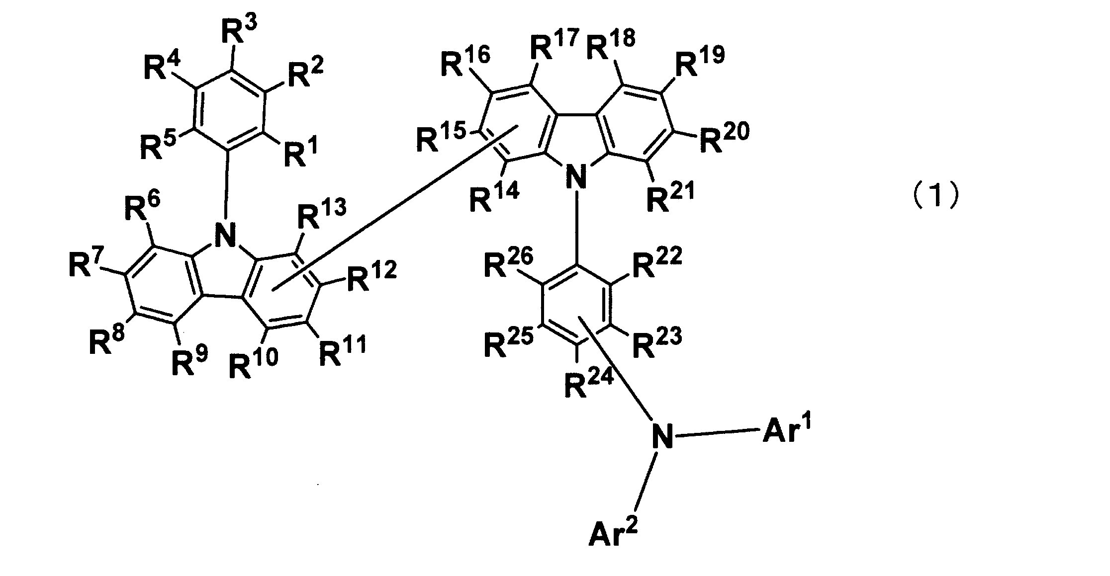
(A)R23またはR25の少なくとも1つがNAr1Ar2であり、その他はそれぞれ同じでも異なっていてもよく、水素、アルキル基、シクロアルキル基、複素環基、アルケニル基、シクロアルケニル基、アルキニル基、ハロゲン、カルボニル基、カルボキシル基、オキシカルボニル基、カルバモイル基、シリル基、および-P(=O)R27R28からなる群より選ばれ、Ar1およびAr2はそれぞれ同じでも異なっていてもよく、置換もしくは無置換のフェニル基を表す。
(B)R24がNAr1Ar2であり、その他はそれぞれ同じでも異なっていてもよく、水素、アルキル基、シクロアルキル基、複素環基、アルケニル基、シクロアルケニル基、アルキニル基、ハロゲン、カルボニル基、カルボキシル基、オキシカルボニル基、カルバモイル基、シリル基、および-P(=O)R27R28からなる群より選ばれ、Ar1およびAr2はそれぞれ同じでも異なっていてもよく、無置換のフェニル基、アルキル基で置換されたフェニル基、ハロゲンで置換されたフェニル基またはフェニル基で置換されたフェニル基を表し、Ar1とAr2が同時にフェニル基で置換されたフェニル基となることはない。)
(A)R23またはR25の少なくとも1つがNAr1Ar2であり、その他はそれぞれ同じでも異なっていてもよく、水素、アルキル基、シクロアルキル基、複素環基、アルケニル基、シクロアルケニル基、アルキニル基、ハロゲン、カルボニル基、カルボキシル基、オキシカルボニル基、カルバモイル基、シリル基、および-P(=O)R27R28からなる群より選ばれ、Ar1およびAr2はそれぞれ同じでも異なっていてもよく、置換もしくは無置換のフェニル基を表す。
(B)R24がNAr1Ar2であり、その他はそれぞれ同じでも異なっていてもよく、水素、アルキル基、シクロアルキル基、複素環基、アルケニル基、シクロアルケニル基、アルキニル基、ハロゲン、カルボニル基、カルボキシル基、オキシカルボニル基、カルバモイル基、シリル基、および-P(=O)R27R28からなる群より選ばれ、Ar1およびAr2はそれぞれ同じでも異なっていてもよく、無置換のフェニル基、アルキル基で置換されたフェニル基、ハロゲンで置換されたフェニル基またはフェニル基で置換されたフェニル基を表し、Ar1とAr2が同時にフェニル基で置換されたフェニル基となることはない。

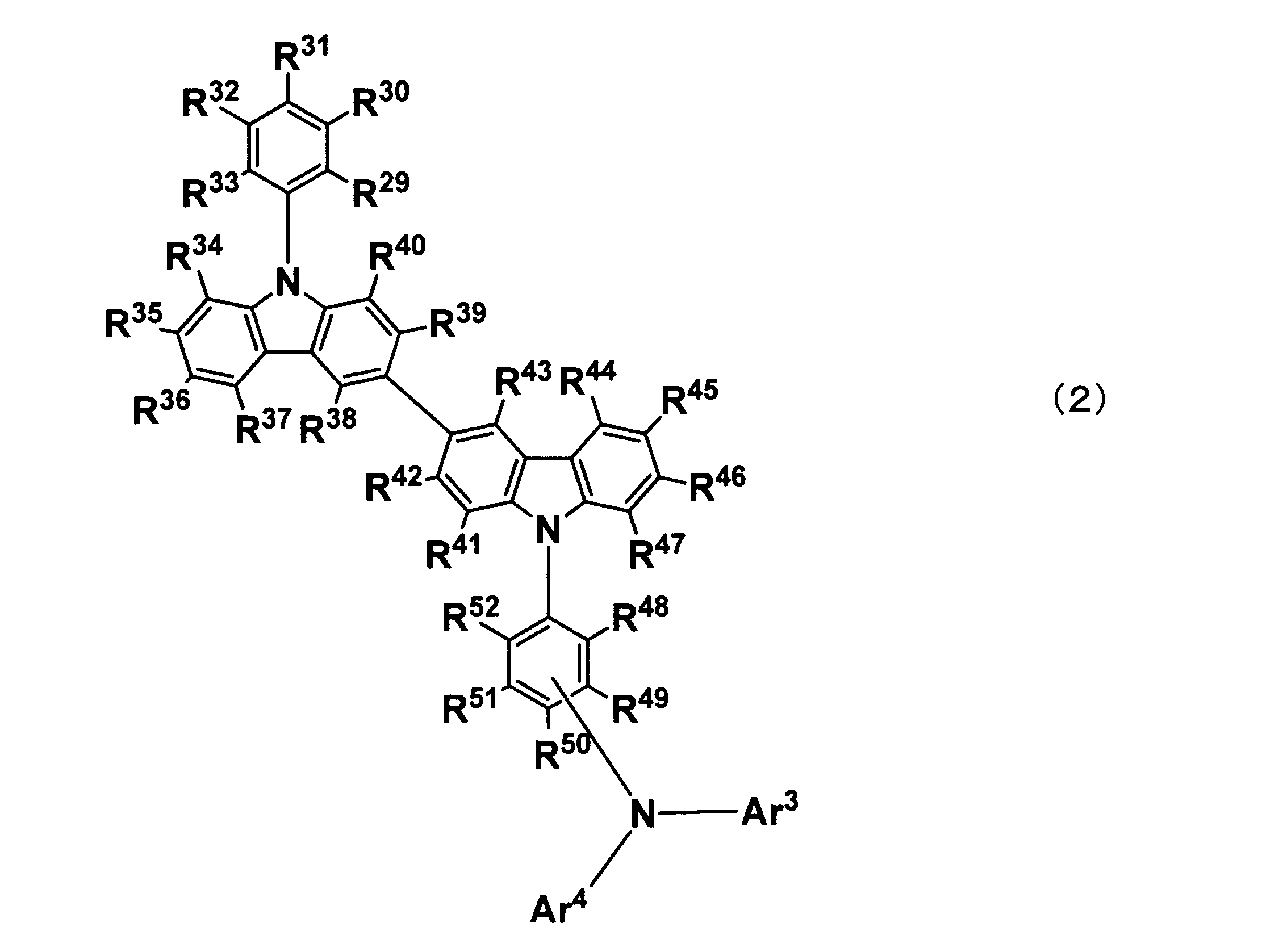
(A’)R49またはR51の少なくとも1つがNAr3Ar4であり、その他はそれぞれ同じでも異なっていてもよく、水素、アルキル基、シクロアルキル基、複素環基、アルケニル基、シクロアルケニル基、アルキニル基、ハロゲン、カルボニル基、カルボキシル基、オキシカルボニル基、カルバモイル基、シリル基、および-P(=O)R53R54からなる群より選ばれ、Ar3およびAr4はそれぞれ同じでも異なっていてもよく、置換もしくは無置換のフェニル基を表す。
(B’)R49またはR51の少なくとも1つがNAr3Ar4であり、その他はそれぞれ同じでも異なっていてもよく、水素、アルキル基、シクロアルキル基、複素環基、アルケニル基、シクロアルケニル基、アルキニル基、ハロゲン、カルボニル基、カルボキシル基、オキシカルボニル基、カルバモイル基、シリル基、および-P(=O)R53R54からなる群より選ばれ、Ar3およびAr4はそれぞれ同じでも異なっていてもよく、無置換のフェニル基、アルキル基で置換されたフェニル基、ハロゲンで置換されたフェニル基またはフェニル基で置換されたフェニル基を表し、Ar3とAr4が同時にフェニル基で置換されたフェニル基となることはない。
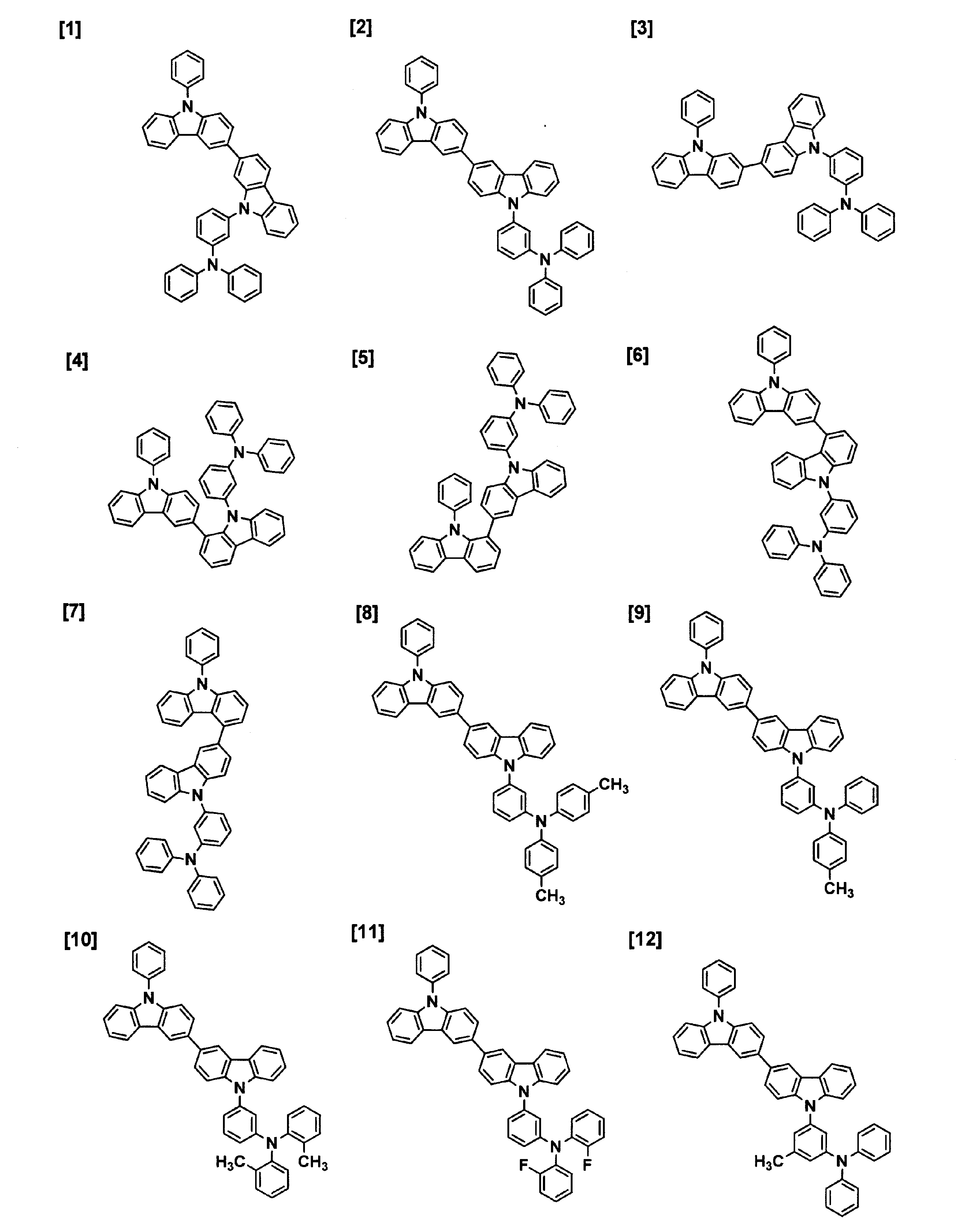


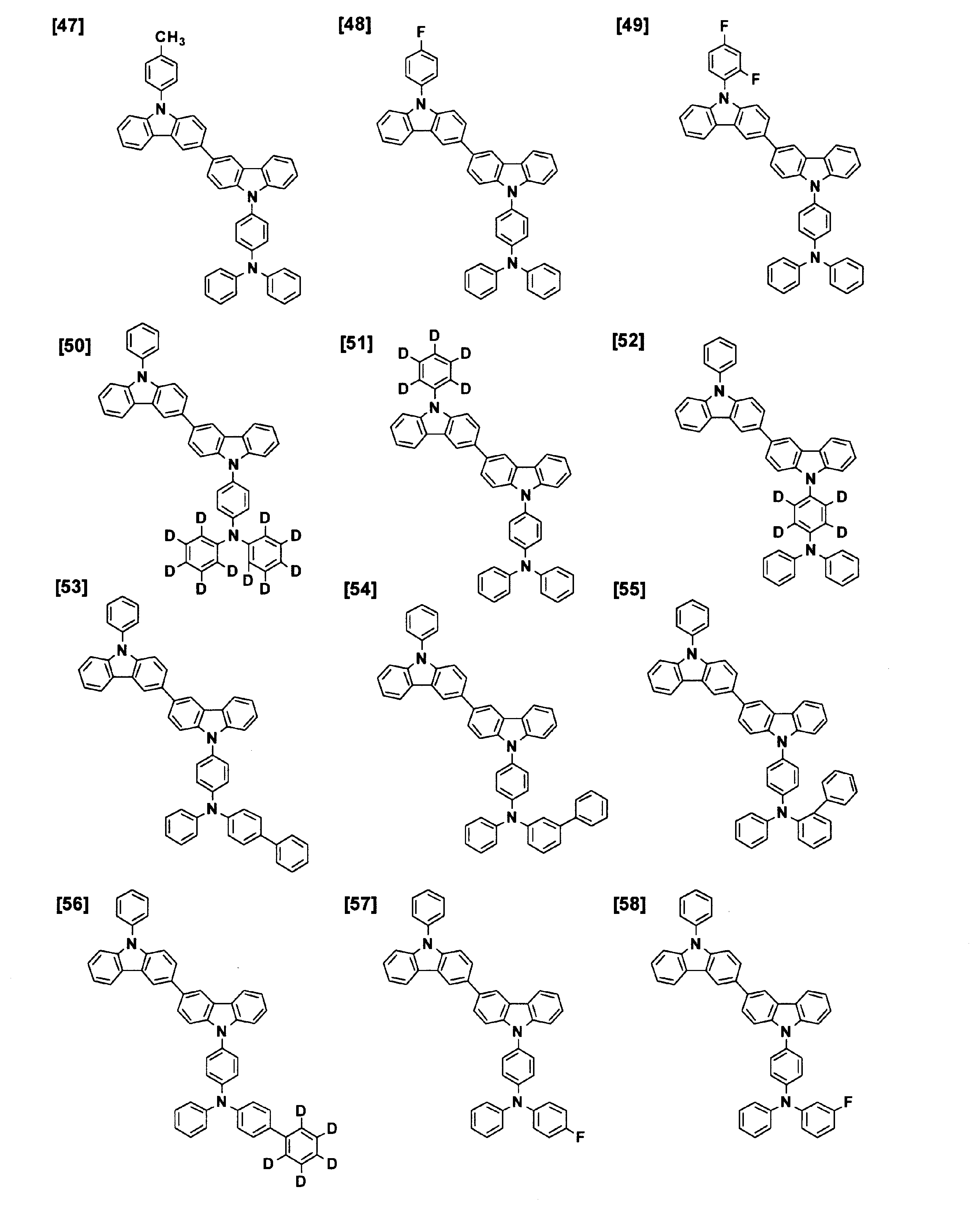
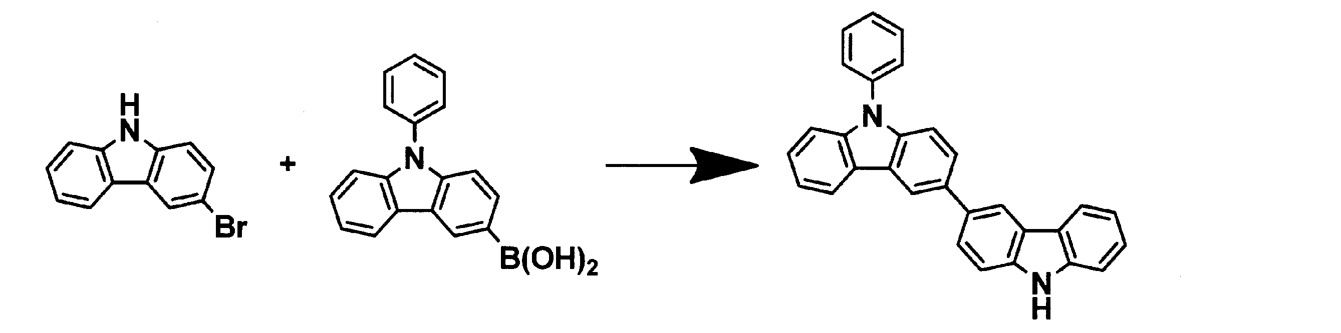
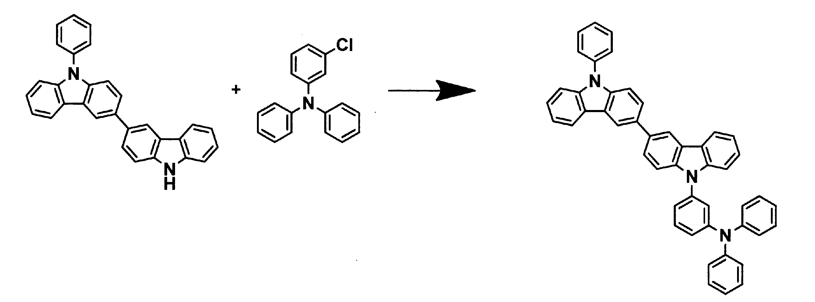
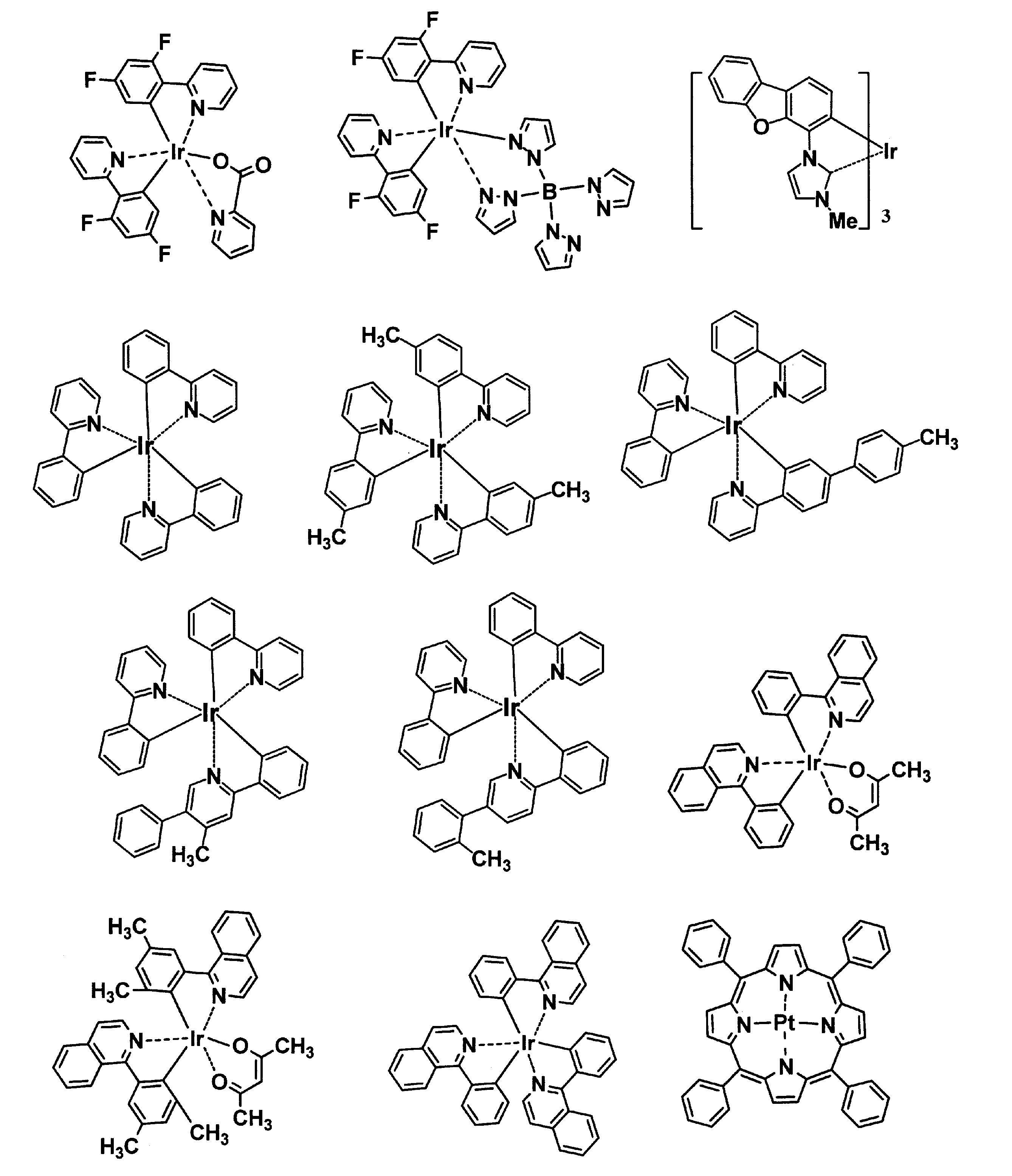
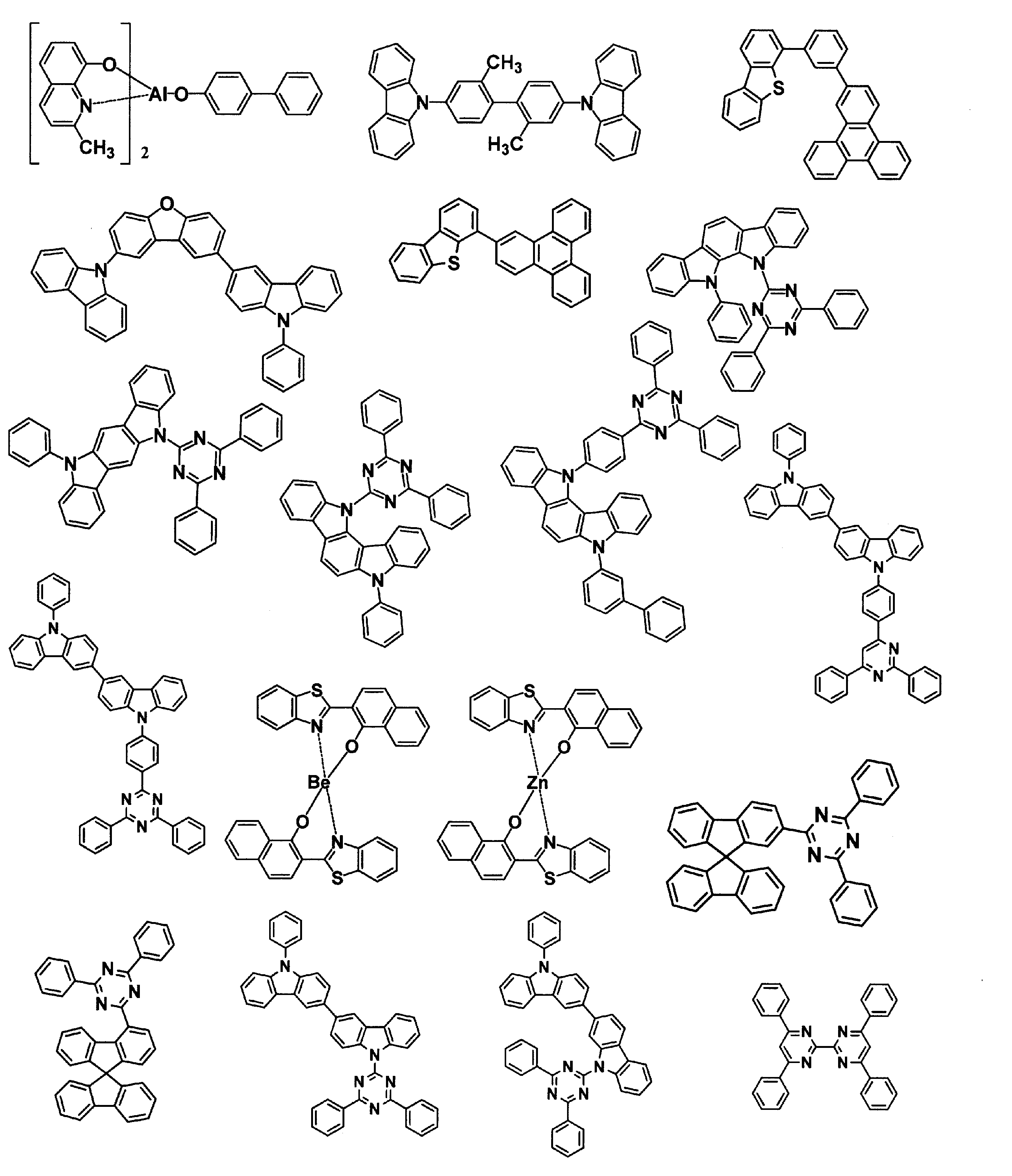
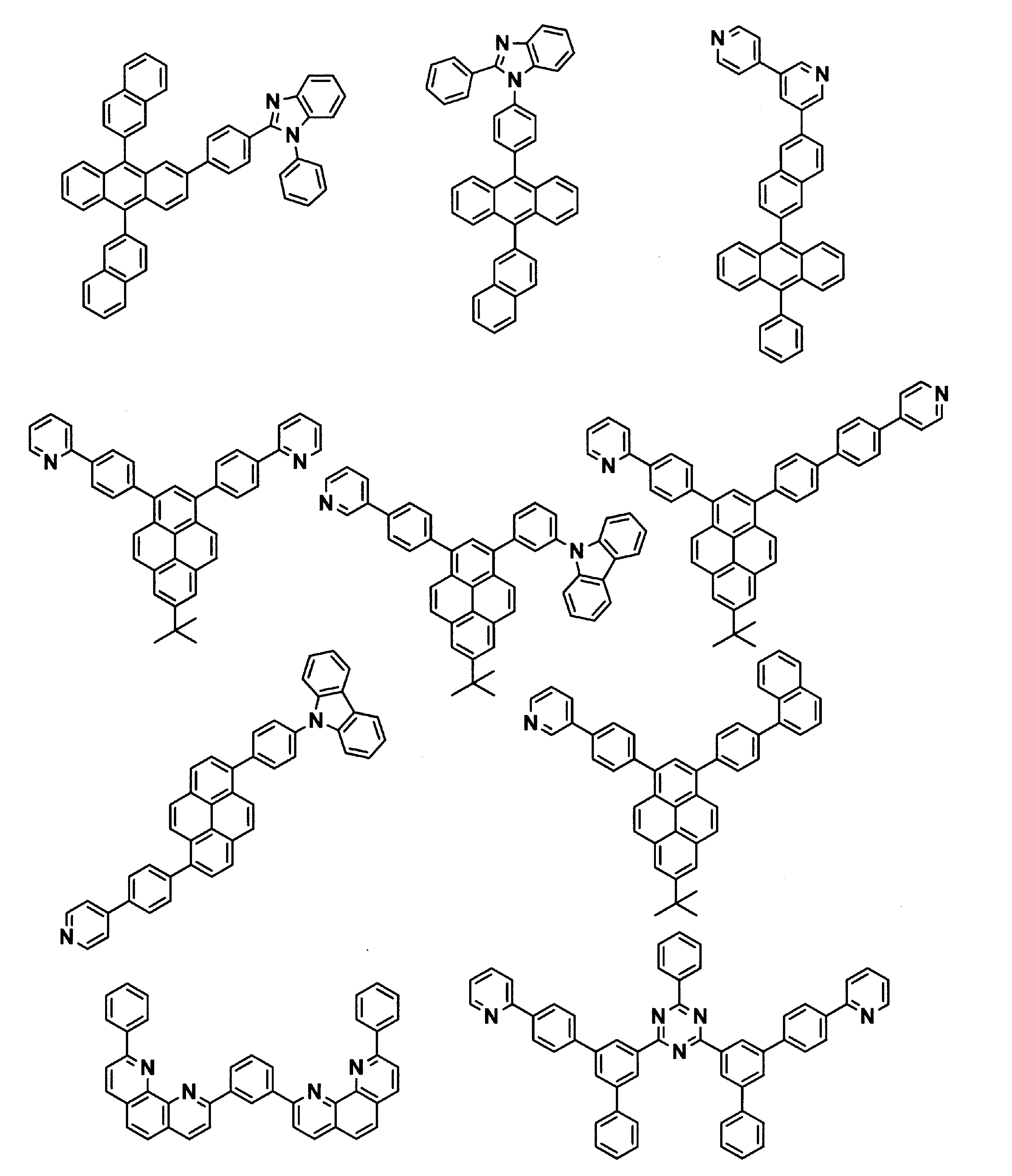
化合物[2]の合成
3-ブロモカルバゾール20.9g、9-フェニルカルバゾール-3-ボロン酸15.0g、酢酸パラジウム366mg、トリス(2-メチルフェニル)ホスフィン300mg、2M炭酸カリウム水溶液105ml、ジメトキシエタン260mlの混合溶液を窒素気流下、6時間還流した。室温に冷却した後、テトラヒドロフラン500mlで抽出した。有機層を飽和食塩水100mlで2回洗浄し、硫酸マグネシウムで乾燥後、エバポレートした。得られた濃縮物をo-キシレン再結晶により精製し、真空乾燥した後、9-フェニル-9H,9’H-3,3’-ビカルバゾール13.5gを得た。
1H-NMR(CDCl3(d=ppm)):7.06(t,2H,J=7.3Hz),7.15-7.35(m,13H),7.39-7.54(m,8H),7.60-7.64(m,4H),7.76(d,2H,J=8.4Hz),8.18-8.26(m,2H),8.43(dd,2H,J=1.6Hz,8.1Hz)。
化合物[8]の合成
3-クロロ-N,N-ジフェニルアニリンの代わりに3-クロロ-N,N-ジ-p-トリルアニリンを用いた以外は合成例1と同様の方法で合成し、白色固体を得た。
1H-NMR(CDCl3(d=ppm)):2.31(s,6H),7.06-7.22(m,10H),7.28-7.67(m,15H),7.74-7.78(m,2H),8.18-8.26(m,2H),8.41-8.45(m,2H)。
化合物[31]の合成
3-ブロモトリフェニルアミンの代わりにN-(3-クロロフェニル)-N-フェニル-[1,1’-ビフェニル]-4-アミンを用いた以外は合成例1と同様の方法で合成し、白色固体を得た。
1H-NMR(CDCl3(d=ppm)):7.06-7.79(m,33 H),8.19-8.25(m,2H),8.41-8.44(m,2H)。
化合物[32]の合成
3-ブロモトリフェニルアミンの代わりにN-(3-クロロフェニル)-N-フェニル-[1,1’-ビフェニル]-3-アミンを用いた以外は合成例1と同様の方法で合成し、白色固体を得た。
1H-NMR(CDCl3(d=ppm)):7.06-7.76(m,33 H),8.17-8.26(m,2H),8.39-8.42(m,2H)。
化合物[33]の合成
3-クロロアニリン3.2g、ブロモベンゼン-d5 8.9g、ナトリウムtert-ブトキシド5.3g、ビス(ジベンジリデンアセトン)パラジウム431mg、トリ-tert-ブチルホスホニウムテトラフルオロボレート196mgとトルエン50mlの混合溶液を窒素気流下、50℃で2時間加熱攪拌した。トルエン50mlで抽出し、有機層を水30mlで3回洗浄し、硫酸マグネシウムで乾燥後、エバポレートした。得られた濃縮物をシリカゲルカラムクロマトグラフィーにより精製し、真空乾燥した後、中間体4.5gを得た。
1H-NMR(CDCl3(d=ppm)):7.16-7.77(m,19 H),8.18-8.26(m,2H),8.41-8.44(d,2H,J=8.37)。
化合物[35]の合成
3-ブロモトリフェニルアミンの代わりに4-ブロモトリフェニルアミンを用いた以外は合成例1と同様の方法で合成し、白色固体を得た。
1H-NMR(CDCl3(d=ppm)):7.09(t,2H,J=7.2Hz),7.21-7.27(m,5H),7.30-7.36(m,8H),7.62-7.64(m,4H),7.76-7.81(dt,2H,J=7.8Hz),8.22-8.26(m,2H),8.45(t,2H,J=1.6Hz)。
化合物[40]の合成
4-ヒドロキシカルバゾール4.5g、ジクロロメタン360mlとジイソプロピルアミン3.0gの混合溶液を窒素気流下、0℃に冷やし、無水トリフルオロメタンスルホン酸8.3gを滴下した。この混合溶液を室温で2時間撹拌した後、水50mlを注入し、ジクロロメタン50mlで抽出した。有機層を水50mlで2回洗浄し、硫酸マグネシウムで乾燥後、エバポレートした。シリカゲルカラムクロマトグラフィーにより精製し、真空乾燥した後、9H-カルバゾール-4-イルトリフルオロメタンスルホナート7.0gを得た。
1H-NMR(CDCl3(d=ppm)):6.92-6.97(m,2H),7.07-7.74(m,27H),8.13-8.16(d,2H,J=7.83),8.43-8.44(d,2H,J=13.5)。
化合物[50]の合成
4-クロロアニリン3.2g、ブロモベンゼン-d5 8.9g、ナトリウムtert-ブトキシド5.3g、ビス(ジベンジリデンアセトン)パラジウム431mg、トリ-tert-ブチルホスホニウムテトラフルオロボレート196mgとトルエン50mlの混合溶液を窒素気流下、50℃で2時間加熱攪拌した。トルエン50mlで抽出し、有機層を水30mlで3回洗浄し、硫酸マグネシウムで乾燥後、エバポレートした。得られた濃縮物をシリカゲルカラムクロマトグラフィーにより精製し、真空乾燥した後、中間体4.5gを得た。
1H-NMR(CDCl3(d=ppm)):7.29-7.79(m,19 H),8.23-8.26(m,2H),8.45(s,2H)。
化合物[53]の合成
3-ブロモトリフェニルアミンの代わりにN-(4-クロロフェニル)-N-フェニル-[1,1’-ビフェニル]-4-アミンを用いた以外は合成例1と同様の方法で合成し、白色固体を得た。
1H-NMR(CDCl3(d=ppm)):7.12-7.62(m,31H),7.77-7.78(m,2H),8.23-8.26(d,2H,J=7.29),8.46(s,2H)。
ITO透明導電膜を50nm堆積させたガラス基板(ジオマテック(株)製、11Ω/□、スパッタ品)を38×46mmに切断し、エッチングを行った。得られた基板を “セミコクリーン56”(商品名、フルウチ化学(株)製)で15分間超音波洗浄してから、超純水で洗浄した。この基板を素子を作製する直前に1時間UV-オゾン処理し、真空蒸着装置内に設置して、装置内の真空度が5×10⁻⁴Pa以下になるまで排気した。抵抗加熱法によって、正孔注入層として化合物HI-1を10nm蒸着した。次に、第一正孔輸送層として、化合物HT-4を80nm蒸着した。次に、第二正孔輸送層として、化合物[2]を10nm蒸着した。次に、発光層として、ホスト材料に化合物H-1を、ドーパント材料に化合物D-1を用い、ドーパント材料のドープ濃度が10重量%になるようにして30nmの厚さに蒸着した。次に、化合物E-1とドナー性材料(Liq:リチウムキノリノール)を蒸着速度比1:1(=0.05nm/s:0.05nm/s)で混合した層を、電子輸送層として35nmの厚さに積層した。
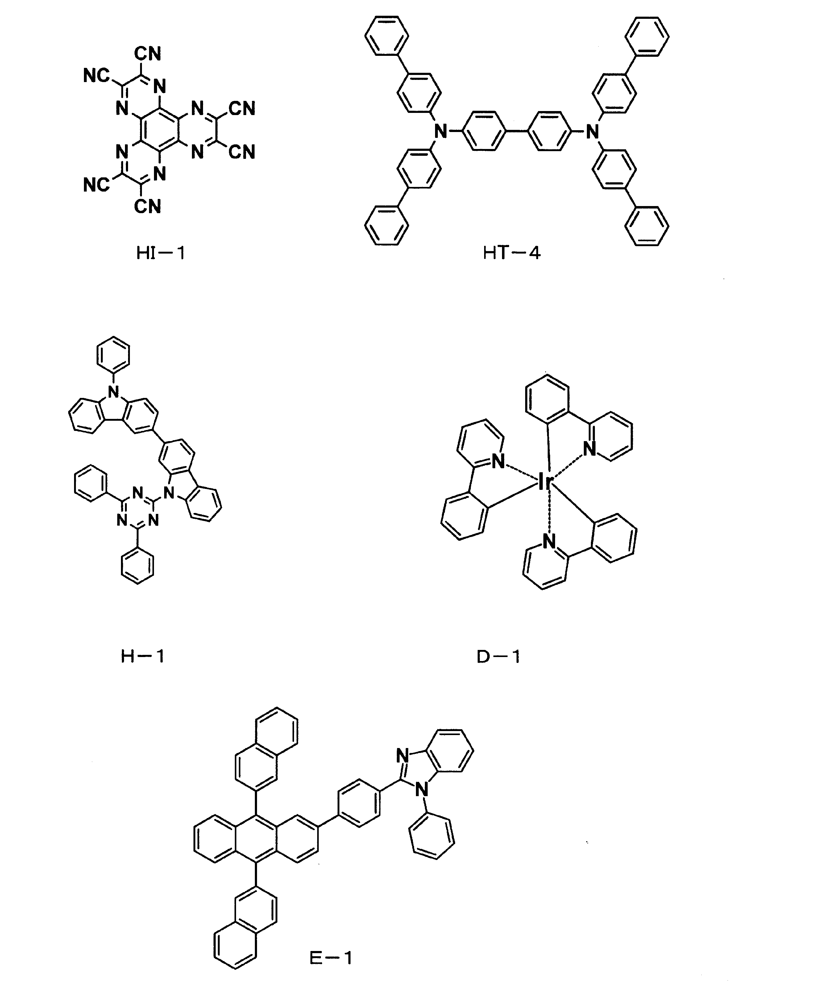
第二正孔輸送層として表2に記載した材料を用いたこと以外は実施例1と同様にして発光素子を作製した。結果を表2に示す。なお、HT-1~HT-7は以下に示す化合物であり、それらの最低励起三重項エネルギーT1は表1に示すとおりである。
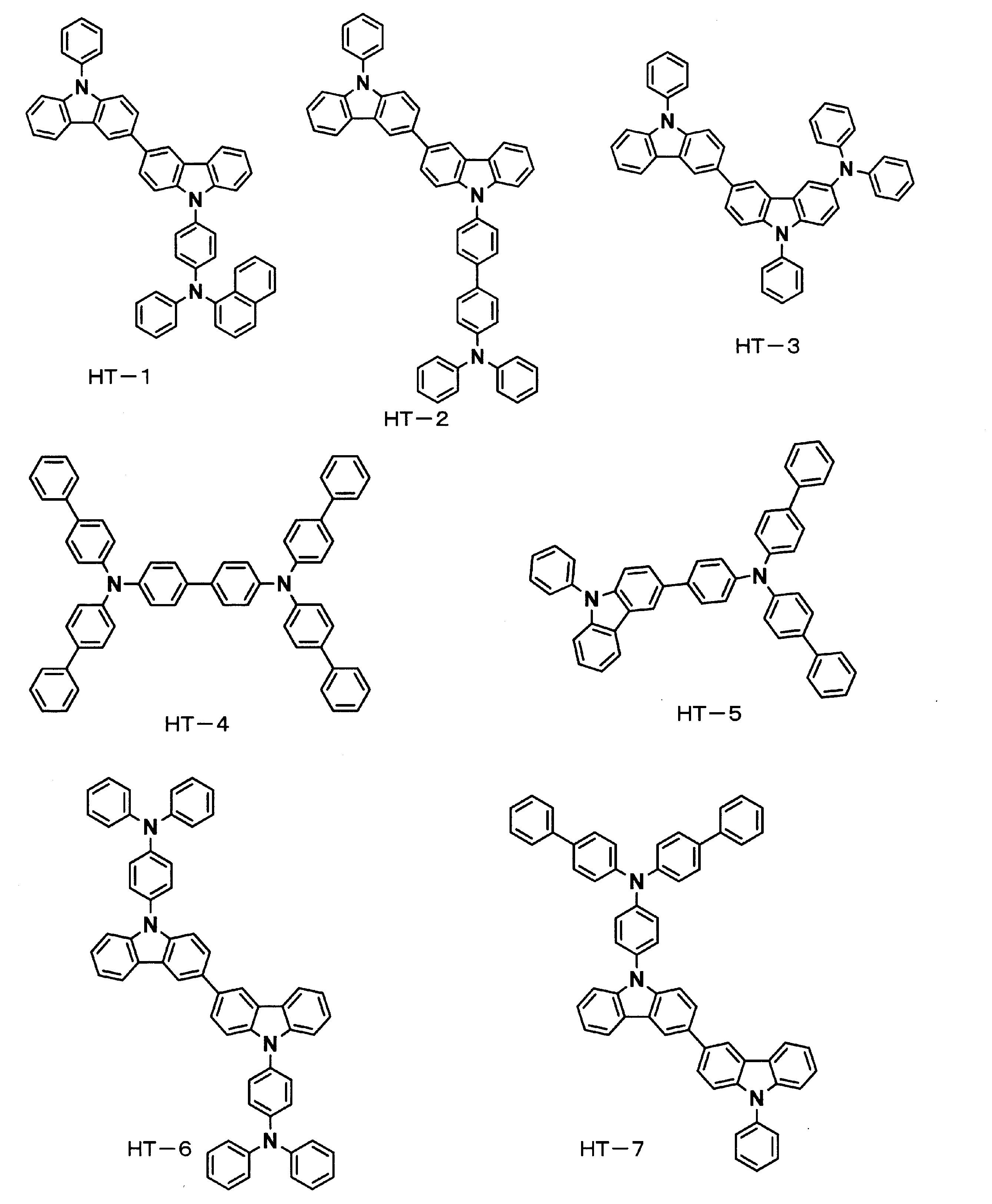

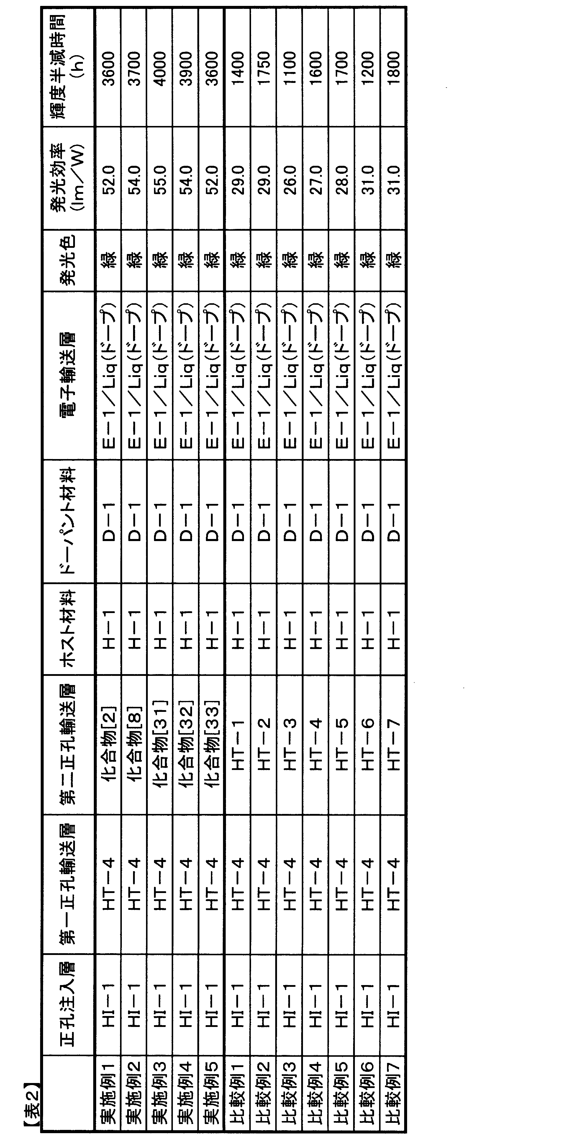
第二正孔輸送層として表2に記載した材料を用い、ホスト材料に化合物H-1の代わりに化合物H-2と化合物H-3の混合ホストを用いたこと以外は実施例1と同様にして発光素子を作製した。化合物H-2と化合物H-3の共蒸着膜を蒸着速度比が1:1で蒸着され、さらにドーパントがドープ濃度が10重量%となるように蒸着されるようにした。結果を表3に示す。なお、H-2、H-3は以下に示す化合物である。

第二正孔輸送層として表2に記載した材料を用い、電子輸送層を二層積層構成とし、第一電子輸送層として化合物E-2を10nmの厚さに蒸着し、第二電子輸送層として化合物E-3とドナー性金属(Li:リチウム)の共蒸着膜を蒸着速度比100:1(=0.2nm/s:0.002nm/s)で25nmの厚さに蒸着して積層した以外は実施例1と同様にして発光素子を作製した。結果を表3に示す。なお、E-2、E-3は以下に示す化合物である。
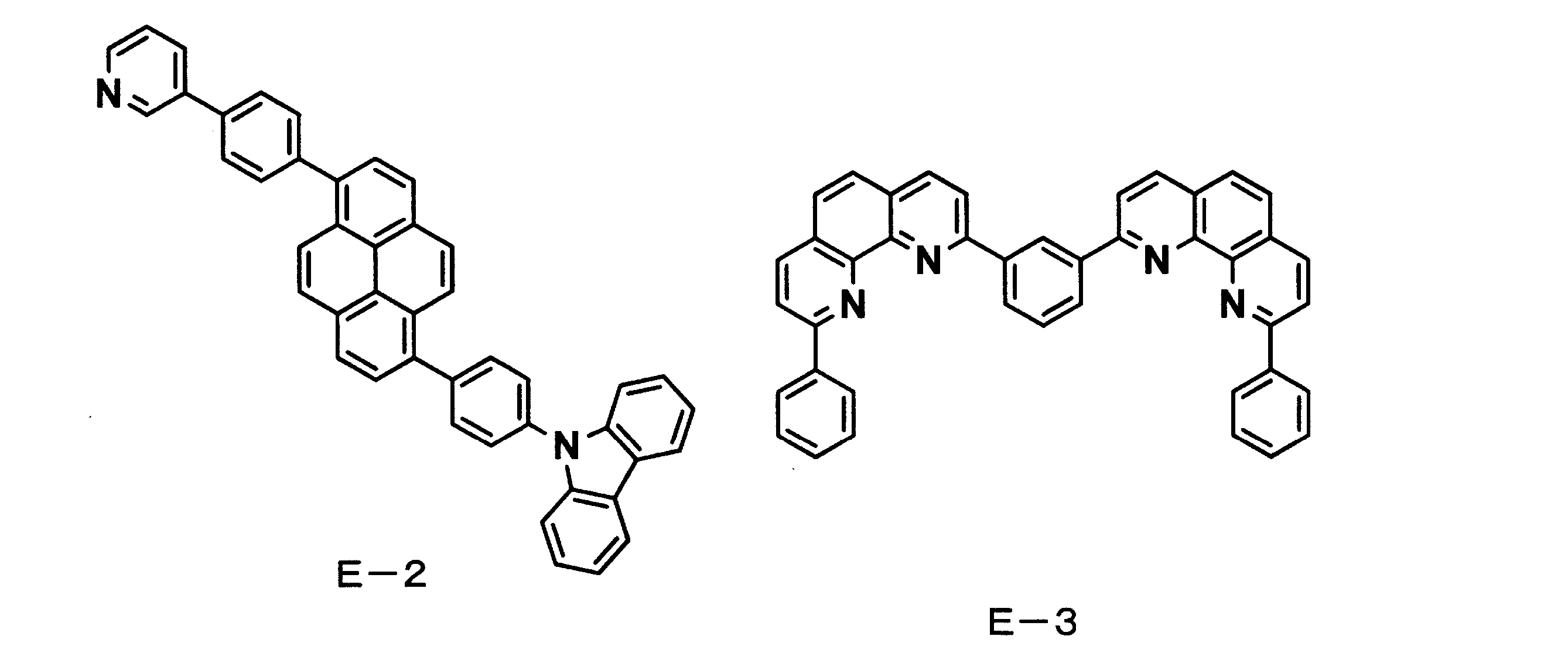
第二正孔輸送層として表2に記載した材料を用い、正孔注入層として、化合物HI-1の代わりに化合物[2]と化合物HI-2を用い、正孔注入層内の化合物[2]に対して化合物HI-2のドープ濃度が5重量%になるようにして10nm蒸着したこと以外は実施例1と同様にして発光素子を作製した。結果を表3に示す。なお、HI-2は以下に示す化合物である。

ITO透明導電膜を50nm堆積させたガラス基板(ジオマテック(株)製、11Ω/□、スパッタ品)を38×46mmに切断し、エッチングを行った。得られた基板を “セミコクリーン56”(商品名、フルウチ化学(株)製)で15分間超音波洗浄してから、超純水で洗浄した。この基板を素子を作製する直前に1時間UV-オゾン処理し、真空蒸着装置内に設置して、装置内の真空度が5×10⁻⁴Pa以下になるまで排気した。抵抗加熱法によって、正孔注入層として化合物HI-1を10nm蒸着した。次に、第一正孔輸送層として、化合物HT-4を80nm蒸着した。次に、第二正孔輸送層として、化合物[2]を10nm蒸着した。次に、発光層として、ホスト材料に化合物H-2を、ドーパント材料に化合物D-2を用い、ドーパント材料のドープ濃度が10重量%になるようにして30nmの厚さに蒸着した。次に、電子輸送層として、化合物E-3を35nmの厚さに積層した。
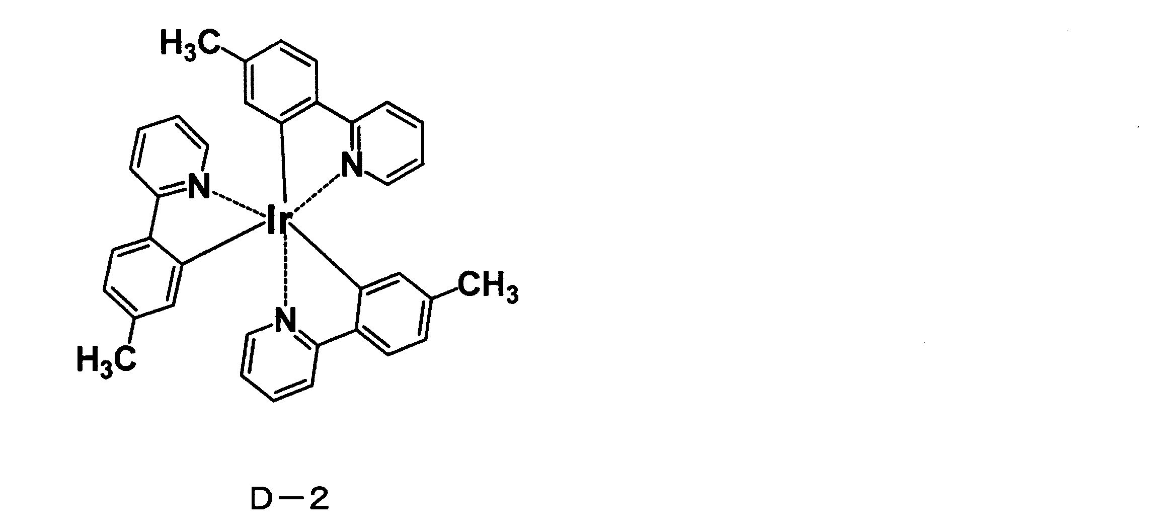
ホスト材料に化合物H-2の代わりに化合物H-2と化合物H-3の混合ホストを用いたこと以外はそれぞれ実施例15と同様にして発光素子を作製した。化合物H-2と化合物H-3の共蒸着膜を蒸着速度比が1:1で蒸着され、さらにドーパントがドープ濃度が10重量%となるように蒸着されるようにした。結果を表3に示す。
電子輸送層として、化合物E-3の代わりに化合物E-1とドナー性材料(Liq:リチウムキノリノール)を混合した層を、蒸着速度比1:1(=0.05nm/s:0.05nm/s)で蒸着して積層した以外はそれぞれ実施例15と同様にして発光素子を作製した。結果を表3に示す。
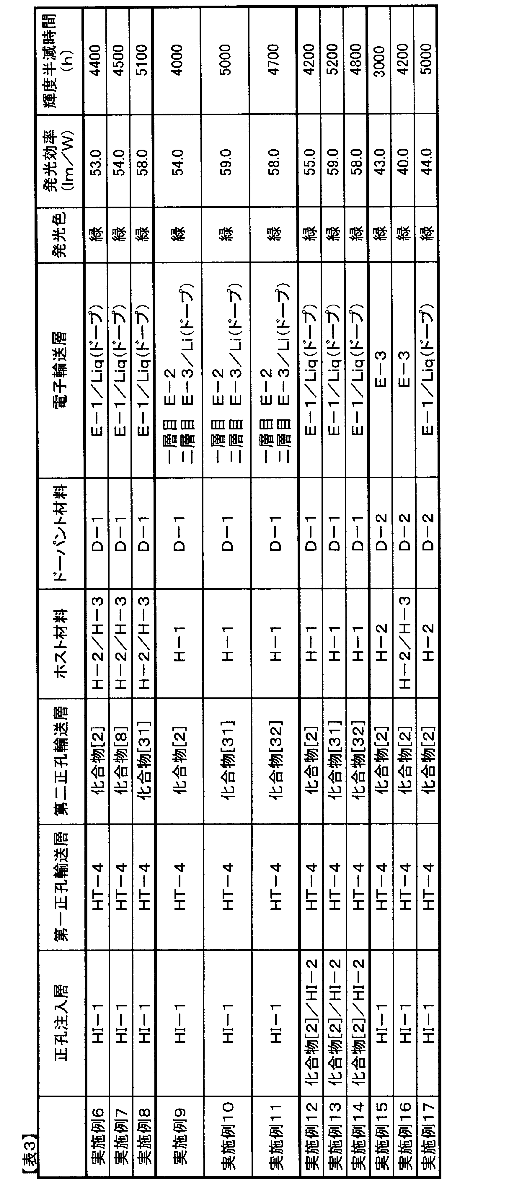
ITO透明導電膜を50nm堆積させたガラス基板(ジオマテック(株)製、11Ω/□、スパッタ品)を38×46mmに切断し、エッチングを行った。得られた基板を “セミコクリーン56”(商品名、フルウチ化学(株)製)で15分間超音波洗浄してから、超純水で洗浄した。この基板を素子を作製する直前に1時間UV-オゾン処理し、真空蒸着装置内に設置して、装置内の真空度が5×10⁻⁴Pa以下になるまで排気した。抵抗加熱法によって、正孔注入層として化合物HI-1を10nm蒸着した。次に、第一正孔輸送層として、化合物HT-4を50nm蒸着した。次に、第二正孔輸送層として、化合物[2]を40nm蒸着した。次に、発光層として、ホスト材料に化合物H-4を、ドーパント材料に化合物D-3を用い、ドーパント材料のドープ濃度が5重量%になるようにして30nmの厚さに蒸着した。次に、電子輸送層として、化合物E-3を35nmの厚さに積層した。
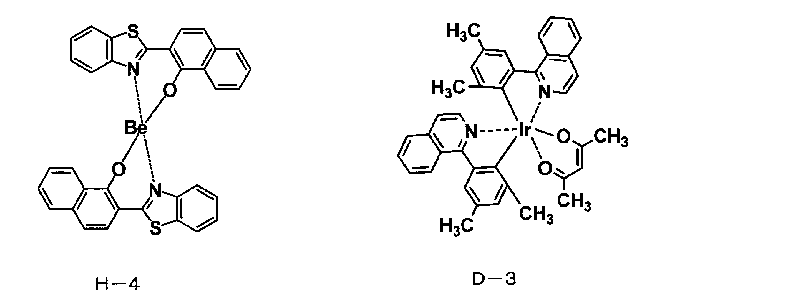
第二正孔輸送層として表4に記載した材料を用いたこと以外は実施例18と同様にして発光素子を作製し、評価した。結果を表4に示す。
第二正孔輸送層として表4に記載した化合物を用いたこと以外は実施例18と同様にして発光素子を作製し、評価した。結果を表4に示す。
第二正孔輸送層として表4に記載した材料を用い、電子輸送層を二層積層構成とし、第一電子輸送層として化合物E-4を25nmの厚さに蒸着し、第二電子輸送層として化合物E-3を10nmの厚さに蒸着して積層した以外は実施例18と同様にして発光素子を作製し、評価した。結果を表4に示す。

ITO透明導電膜を50nm堆積させたガラス基板(ジオマテック(株)製、11Ω/□、スパッタ品)を38×46mmに切断し、エッチングを行った。得られた基板を “セミコクリーン56”(商品名、フルウチ化学(株)製)で15分間超音波洗浄してから、超純水で洗浄した。この基板を素子を作製する直前に1時間UV-オゾン処理し、真空蒸着装置内に設置して、装置内の真空度が5×10⁻⁴Pa以下になるまで排気した。抵抗加熱法によって、正孔注入層としてHI-1を10nm蒸着した。次に、第一正孔輸送層として、HT-4を110nm蒸着した。次に、第二正孔輸送層として、化合物[2]を10nm蒸着した。次に、発光層として、ホスト材料に化合物H-5を、ドーパント材料に化合物D-4を用い、ドーパント材料のドープ濃度が5重量%になるようにして40nmの厚さに蒸着した。次に、化合物E-1とドナー性材料(Liq:リチウムキノリノール)を蒸着速度比1:1(=0.05nm/s:0.05nm/s)で混合した層を、電子輸送層として35nmの厚さに積層した。

第二正孔輸送層として表5に記載した材料を用いたこと以外は実施例23と同様にして発光素子を作製し、評価した。結果を表5に示す。
第二正孔輸送層として表5に記載した材料を用い、電子輸送層を二層積層構成とし、第一電子輸送層として、化合物E-4または化合物E-2を25nmの厚さに蒸着し、第二電子輸送層としてE-3を10nmの厚さに蒸着して積層した以外は実施例23と同様にして発光素子を作製し、評価した。結果を表5に示す。

第二正孔輸送層として表6に記載した材料を用いたこと以外は実施例1と同様にして発光素子を作製した。結果を表6に示す。
第二正孔輸送層として表6に記載した材料を用い、ホスト材料に化合物H-1の代わりに化合物H-2と化合物H-3の混合ホストを用いたこと以外は実施例1と同様にして発光素子を作製した。化合物H-2と化合物H-3の共蒸着膜を蒸着速度比が1:1で蒸着され、さらにドーパントがドープ濃度が10重量%となるように蒸着されるようにした。結果を表6に示す。
第二正孔輸送層として表6に記載した材料を用い、電子輸送層を二層積層構成とし、第一電子輸送層として化合物E-2を10nmの厚さに蒸着し、第二電子輸送層として化合物E-3とドナー性金属(Li:リチウム)の共蒸着膜を蒸着速度比100:1(=0.2nm/s:0.002nm/s)で25nmの厚さに蒸着して積層した以外は実施例1と同様にして発光素子を作製した。結果を表6に示す。
第二正孔輸送層として表6に記載した材料を用い、正孔注入層として、化合物HI-1の代わりに化合物[53]と化合物HI-2を用い、正孔注入層内の化合物[53]に対して化合物HI-2のドープ濃度が2重量%になるようにして10nm蒸着したこと以外は実施例1と同様にして発光素子を作製した。結果を表6に示す。
第二正孔輸送層として化合物[2]の代わりに化合物[35]を用いたこと以外は実施例15と同様にして発光素子を作製した。結果を表6に示す。
第二正孔輸送層として化合物[2]の代わりに化合物[35]を用いたこと以外は実施例16と同様にして発光素子を作製した。結果を表6に示す。
第二正孔輸送層として化合物[2]の代わりに化合物[35]を用いたこと以外は実施例17と同様にして発光素子を作製した。結果を表6に示す。

Claims (16)
- 下記一般式(1)で表される化合物を含有することを特徴とする発光素子材料。

(A)R23またはR25の少なくとも1つがNAr1Ar2であり、その他はそれぞれ同じでも異なっていてもよく、水素、アルキル基、シクロアルキル基、複素環基、アルケニル基、シクロアルケニル基、アルキニル基、ハロゲン、カルボニル基、カルボキシル基、オキシカルボニル基、カルバモイル基、シリル基、および-P(=O)R27R28からなる群より選ばれ、Ar1およびAr2はそれぞれ同じでも異なっていてもよく、置換もしくは無置換のフェニル基を表す。
(B)R24がNAr1Ar2であり、その他はそれぞれ同じでも異なっていてもよく、水素、アルキル基、シクロアルキル基、複素環基、アルケニル基、シクロアルケニル基、アルキニル基、ハロゲン、カルボニル基、カルボキシル基、オキシカルボニル基、カルバモイル基、シリル基、および-P(=O)R27R28からなる群より選ばれ、Ar1およびAr2はそれぞれ同じでも異なっていてもよく、無置換のフェニル基、アルキル基で置換されたフェニル基、ハロゲンで置換されたフェニル基またはフェニル基で置換されたフェニル基を表し、Ar1とAr2が同時にフェニル基で置換されたフェニル基となることはない。) - 前記一般式(1)で表される化合物の三重項エネルギーが2.60eV以上である請求項1記載の発光素子材料。
- 前記一般式(1)で表される化合物が、下記一般式(2)で表される化合物である請求項1または2記載の発光素子材料。
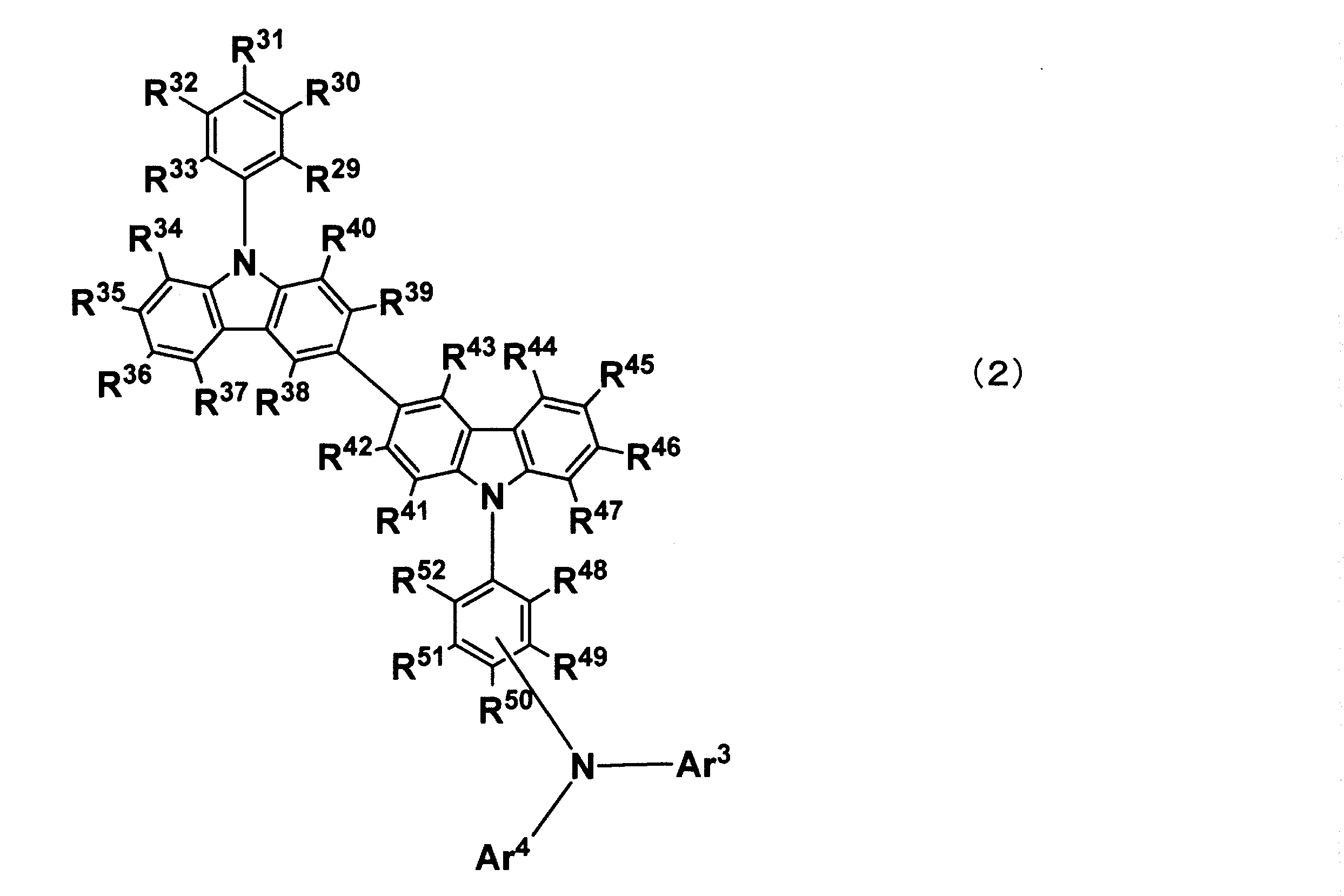
(A’)R49またはR51の少なくとも1つがNAr3Ar4であり、その他はそれぞれ同じでも異なっていてもよく、水素、アルキル基、シクロアルキル基、複素環基、アルケニル基、シクロアルケニル基、アルキニル基、ハロゲン、カルボニル基、カルボキシル基、オキシカルボニル基、カルバモイル基、シリル基、および-P(=O)R53R54からなる群より選ばれ、Ar3およびAr4はそれぞれ同じでも異なっていてもよく、置換もしくは無置換のフェニル基を表す。
(B’)R49またはR51の少なくとも1つがNAr3Ar4であり、その他はそれぞれ同じでも異なっていてもよく、水素、アルキル基、シクロアルキル基、複素環基、アルケニル基、シクロアルケニル基、アルキニル基、ハロゲン、カルボニル基、カルボキシル基、オキシカルボニル基、カルバモイル基、シリル基、および-P(=O)R53R54からなる群より選ばれ、Ar3およびAr4はそれぞれ同じでも異なっていてもよく、無置換のフェニル基、アルキル基で置換されたフェニル基、ハロゲンで置換されたフェニル基またはフェニル基で置換されたフェニル基を表し、Ar3とAr4が同時にフェニル基で置換されたフェニル基となることはない。) - 前記一般式(1)において、R22~R26が条件(A)を満たし、Ar1およびAr2が無置換のフェニル基、フェニル基で置換されたフェニル基、アルキル基で置換されたフェニル基、またはハロゲンで置換されたフェニル基である請求項1または2記載の発光素子材料。
- 前記一般式(1)において、R22~R26が条件(A)を満たし、R1~R21が全て水素であり、R22~R26は、R23またはR25のうち1つがNAr1Ar2であり、その他は全て水素である請求項1、2または4のいずれか記載の発光素子材料。
- 前記一般式(1)において、R22~R26が条件(B)を満たし、Ar1およびAr2のどちらか一方が無置換のフェニル基であり、もう一方がアルキル基で置換されたフェニル基、ハロゲンで置換されたフェニル基またはフェニル基で置換されたフェニル基である請求項1または2記載の発光素子材料。
- 前記一般式(1)において、R22~R26が条件(B)を満たし、R1~R21が全て水素であり、R22~R26は、R24がNAr1Ar2であり、その他は全て水素である請求項1、2または6のいずれか記載の発光素子材料。
- Ar1およびAr2が異なることを特徴とする請求項1、2、4または5のいずれか記載の発光素子材料。
- 陽極と陰極の間に有機層が存在し、電気エネルギーにより発光する発光素子であって、前記陽極と陰極の間のいずれかの層に請求項1~8のいずれか記載の発光素子材料を含有することを特徴とする発光素子。
- 前記有機層に少なくとも正孔輸送層が存在し、正孔輸送層に請求項1~8のいずれか記載の発光素子材料を含有する請求項9記載の発光素子。
- 前記有機層に少なくとも正孔注入層が存在し、正孔注入層に請求項1~8のいずれか記載の発光素子材料を含有する請求項9記載の発光素子。
- 前記正孔輸送層と前記陽極の間に正孔注入層が存在し、正孔注入層がアクセプター性材料を含有する請求項11記載の発光素子。
- 前記有機層に少なくとも発光層が存在し、発光層に三重項発光材料を含有する請求項10~12のいずれか記載の発光素子。
- 前記三重項発光材料がイリジウムまたは白金を含む金属錯体である請求項13記載の発光素子。
- 前記有機層に少なくとも電子輸送層が存在し、電子輸送層が、電子受容性窒素を含み、さらに炭素、水素、窒素、酸素、ケイ素、リンの中から選ばれる元素で構成されるヘテロアリール環構造を有する化合物を含有する請求項9~14のいずれか記載の発光素子。
- 前記電子輸送層がドナー性材料を含有することを特徴とする請求項15記載の発光素子。
Priority Applications (5)
| Application Number | Priority Date | Filing Date | Title |
|---|---|---|---|
| EP13749201.3A EP2816626B1 (en) | 2012-02-15 | 2013-02-13 | Light-emitting element material, and light-emitting element |
| US14/377,431 US9627625B2 (en) | 2012-02-15 | 2013-02-13 | Light-emitting device material and light-emitting device |
| KR1020147021023A KR102033951B1 (ko) | 2012-02-15 | 2013-02-13 | 발광 소자 재료 및 발광 소자 |
| JP2013510422A JP5397568B1 (ja) | 2012-02-15 | 2013-02-13 | 発光素子材料および発光素子 |
| CN201380007310.XA CN104094434B (zh) | 2012-02-15 | 2013-02-13 | 发光元件材料及发光元件 |
Applications Claiming Priority (2)
| Application Number | Priority Date | Filing Date | Title |
|---|---|---|---|
| JP2012030176 | 2012-02-15 | ||
| JP2012-030176 | 2012-02-15 |
Publications (1)
| Publication Number | Publication Date |
|---|---|
| WO2013122082A1 true WO2013122082A1 (ja) | 2013-08-22 |
Family
ID=48984192
Family Applications (1)
| Application Number | Title | Priority Date | Filing Date |
|---|---|---|---|
| PCT/JP2013/053347 WO2013122082A1 (ja) | 2012-02-15 | 2013-02-13 | 発光素子材料および発光素子 |
Country Status (7)
| Country | Link |
|---|---|
| US (1) | US9627625B2 (ja) |
| EP (1) | EP2816626B1 (ja) |
| JP (1) | JP5397568B1 (ja) |
| KR (1) | KR102033951B1 (ja) |
| CN (1) | CN104094434B (ja) |
| TW (1) | TWI558693B (ja) |
| WO (1) | WO2013122082A1 (ja) |
Cited By (9)
| Publication number | Priority date | Publication date | Assignee | Title |
|---|---|---|---|---|
| WO2014097711A1 (ja) * | 2012-12-21 | 2014-06-26 | 出光興産株式会社 | 有機エレクトロルミネッセンス素子および電子機器 |
| JP2015227316A (ja) * | 2014-06-02 | 2015-12-17 | 東ソー株式会社 | 4−カルバゾリルアミン化合物 |
| JP2018524797A (ja) * | 2015-06-19 | 2018-08-30 | サムスン エスディアイ カンパニー, リミテッドSamsung Sdi Co., Ltd. | 有機光電子素子用組成物、有機光電子素子および表示装置 |
| WO2018174293A1 (ja) * | 2017-03-24 | 2018-09-27 | 出光興産株式会社 | 有機エレクトロルミネッセンス素子及び電子機器 |
| KR101922178B1 (ko) * | 2017-11-22 | 2018-11-27 | 삼성디스플레이 주식회사 | 유기 발광 소자 |
| JP2019501527A (ja) * | 2015-12-15 | 2019-01-17 | クンシャン ニュー フラット パネル ディスプレイ テクノロジー センター カンパニー リミテッド | 有機発光表示デバイス及び表示装置 |
| WO2019054599A1 (ko) * | 2017-09-15 | 2019-03-21 | (주)피엔에이치테크 | 유기발광 화합물 및 이를 포함하는 유기전계발광소자 |
| US10326080B2 (en) | 2014-02-14 | 2019-06-18 | Samsung Display Co., Ltd. | Organic light-emitting devices |
| KR20230078941A (ko) | 2020-09-30 | 2023-06-05 | 이데미쓰 고산 가부시키가이샤 | 화합물, 유기 전기발광 소자용 재료, 유기 전기발광 소자 및 전자 기기 |
Families Citing this family (5)
| Publication number | Priority date | Publication date | Assignee | Title |
|---|---|---|---|---|
| CN104119264A (zh) * | 2013-04-25 | 2014-10-29 | 海洋王照明科技股份有限公司 | 一种有机半导体材料、制备方法和电致发光器件 |
| KR102126602B1 (ko) * | 2016-04-22 | 2020-06-24 | 주식회사 엘지화학 | 카바졸 유도체 및 이를 이용한 유기 발광 소자 |
| KR102157756B1 (ko) * | 2016-12-12 | 2020-09-18 | 엘지디스플레이 주식회사 | 유기 화합물과 이를 포함하는 유기발광다이오드 및 유기발광 표시장치 |
| JP7149263B2 (ja) * | 2017-03-28 | 2022-10-06 | 保土谷化学工業株式会社 | 有機エレクトロルミネッセンス素子 |
| CN111384299B (zh) * | 2018-12-29 | 2024-02-09 | 固安鼎材科技有限公司 | 一种有机发光二极管及其制备方法 |
Citations (13)
| Publication number | Priority date | Publication date | Assignee | Title |
|---|---|---|---|---|
| JPH083547A (ja) | 1994-03-31 | 1996-01-09 | Toray Ind Inc | 発光素子 |
| JPH09249876A (ja) * | 1996-03-18 | 1997-09-22 | Toray Ind Inc | 発光素子 |
| WO2006061759A2 (en) | 2004-12-08 | 2006-06-15 | Koninklijke Philips Electronics N.V. | 9 , 9 ' - and 2 , 2 ' -substituted 3 , 3 ' -bicarbazolyl derivatives for use in semiconducting materials as a host matrix for phosphorescent emitters |
| JP2008135498A (ja) * | 2006-11-28 | 2008-06-12 | Toray Ind Inc | 発光素子 |
| JP2009130141A (ja) | 2007-11-22 | 2009-06-11 | Idemitsu Kosan Co Ltd | 有機el素子および有機el材料含有溶液 |
| KR20090112137A (ko) * | 2008-04-23 | 2009-10-28 | 주식회사 이엘엠 | 유기 전기 발광 조성물 및 이를 포함하는 유기 전기 발광소자 |
| KR20100079458A (ko) | 2008-12-31 | 2010-07-08 | 덕산하이메탈(주) | 비스-카바졸 화합물 및 이를 이용한 유기전기소자, 그 단말 |
| WO2010095621A1 (ja) | 2009-02-18 | 2010-08-26 | 出光興産株式会社 | 芳香族アミン誘導体及び有機エレクトロルミネッセンス素子 |
| WO2011024451A1 (ja) * | 2009-08-28 | 2011-03-03 | 保土谷化学工業株式会社 | カルバゾール環構造を有する化合物および有機エレクトロルミネッセンス素子 |
| WO2011055934A2 (ko) * | 2009-11-03 | 2011-05-12 | 제일모직 주식회사 | 유기광전소자용 화합물 및 이를 포함하는 유기광전소자 |
| WO2011139055A2 (ko) * | 2010-05-03 | 2011-11-10 | 제일모직 주식회사 | 유기광전자소자용 화합물, 이를 포함하는 유기발광소자 및 상기 유기발광소자를 포함하는 표시장치 |
| WO2011162162A1 (ja) * | 2010-06-24 | 2011-12-29 | 東レ株式会社 | 発光素子材料および発光素子 |
| WO2012001986A1 (ja) | 2010-06-30 | 2012-01-05 | 保土谷化学工業株式会社 | カルバゾール環構造を有する化合物および有機エレクトロルミネッセンス素子 |
Family Cites Families (2)
| Publication number | Priority date | Publication date | Assignee | Title |
|---|---|---|---|---|
| KR20050118098A (ko) * | 2004-03-19 | 2005-12-15 | 주식회사 엘지화학 | 새로운 정공 주입 또는 수송용 물질 및 이를 이용한 유기발광 소자 |
| US7723722B2 (en) * | 2007-03-23 | 2010-05-25 | Semiconductor Energy Laboratory Co., Ltd. | Organic compound, anthracene derivative, and light-emitting element, light-emitting device, and electronic device using anthracene derivative |
-
2013
- 2013-02-13 US US14/377,431 patent/US9627625B2/en active Active
- 2013-02-13 CN CN201380007310.XA patent/CN104094434B/zh active Active
- 2013-02-13 KR KR1020147021023A patent/KR102033951B1/ko active IP Right Grant
- 2013-02-13 EP EP13749201.3A patent/EP2816626B1/en active Active
- 2013-02-13 WO PCT/JP2013/053347 patent/WO2013122082A1/ja active Application Filing
- 2013-02-13 JP JP2013510422A patent/JP5397568B1/ja active Active
- 2013-02-18 TW TW102105546A patent/TWI558693B/zh active
Patent Citations (13)
| Publication number | Priority date | Publication date | Assignee | Title |
|---|---|---|---|---|
| JPH083547A (ja) | 1994-03-31 | 1996-01-09 | Toray Ind Inc | 発光素子 |
| JPH09249876A (ja) * | 1996-03-18 | 1997-09-22 | Toray Ind Inc | 発光素子 |
| WO2006061759A2 (en) | 2004-12-08 | 2006-06-15 | Koninklijke Philips Electronics N.V. | 9 , 9 ' - and 2 , 2 ' -substituted 3 , 3 ' -bicarbazolyl derivatives for use in semiconducting materials as a host matrix for phosphorescent emitters |
| JP2008135498A (ja) * | 2006-11-28 | 2008-06-12 | Toray Ind Inc | 発光素子 |
| JP2009130141A (ja) | 2007-11-22 | 2009-06-11 | Idemitsu Kosan Co Ltd | 有機el素子および有機el材料含有溶液 |
| KR20090112137A (ko) * | 2008-04-23 | 2009-10-28 | 주식회사 이엘엠 | 유기 전기 발광 조성물 및 이를 포함하는 유기 전기 발광소자 |
| KR20100079458A (ko) | 2008-12-31 | 2010-07-08 | 덕산하이메탈(주) | 비스-카바졸 화합물 및 이를 이용한 유기전기소자, 그 단말 |
| WO2010095621A1 (ja) | 2009-02-18 | 2010-08-26 | 出光興産株式会社 | 芳香族アミン誘導体及び有機エレクトロルミネッセンス素子 |
| WO2011024451A1 (ja) * | 2009-08-28 | 2011-03-03 | 保土谷化学工業株式会社 | カルバゾール環構造を有する化合物および有機エレクトロルミネッセンス素子 |
| WO2011055934A2 (ko) * | 2009-11-03 | 2011-05-12 | 제일모직 주식회사 | 유기광전소자용 화합물 및 이를 포함하는 유기광전소자 |
| WO2011139055A2 (ko) * | 2010-05-03 | 2011-11-10 | 제일모직 주식회사 | 유기광전자소자용 화합물, 이를 포함하는 유기발광소자 및 상기 유기발광소자를 포함하는 표시장치 |
| WO2011162162A1 (ja) * | 2010-06-24 | 2011-12-29 | 東レ株式会社 | 発光素子材料および発光素子 |
| WO2012001986A1 (ja) | 2010-06-30 | 2012-01-05 | 保土谷化学工業株式会社 | カルバゾール環構造を有する化合物および有機エレクトロルミネッセンス素子 |
Non-Patent Citations (1)
| Title |
|---|
| See also references of EP2816626A4 |
Cited By (13)
| Publication number | Priority date | Publication date | Assignee | Title |
|---|---|---|---|---|
| JP2014123687A (ja) * | 2012-12-21 | 2014-07-03 | Idemitsu Kosan Co Ltd | 有機エレクトロルミネッセンス素子および電子機器 |
| WO2014097711A1 (ja) * | 2012-12-21 | 2014-06-26 | 出光興産株式会社 | 有機エレクトロルミネッセンス素子および電子機器 |
| US10326080B2 (en) | 2014-02-14 | 2019-06-18 | Samsung Display Co., Ltd. | Organic light-emitting devices |
| US10333077B2 (en) | 2014-02-14 | 2019-06-25 | Samsung Display Co., Ltd. | Organic light-emitting devices |
| JP2015227316A (ja) * | 2014-06-02 | 2015-12-17 | 東ソー株式会社 | 4−カルバゾリルアミン化合物 |
| JP2018524797A (ja) * | 2015-06-19 | 2018-08-30 | サムスン エスディアイ カンパニー, リミテッドSamsung Sdi Co., Ltd. | 有機光電子素子用組成物、有機光電子素子および表示装置 |
| US10644245B2 (en) | 2015-06-19 | 2020-05-05 | Samsung Sdi Co., Ltd. | Composition for organic photoelectronic element, organic photoelectronic element, and display apparatus |
| JP2019501527A (ja) * | 2015-12-15 | 2019-01-17 | クンシャン ニュー フラット パネル ディスプレイ テクノロジー センター カンパニー リミテッド | 有機発光表示デバイス及び表示装置 |
| WO2018174293A1 (ja) * | 2017-03-24 | 2018-09-27 | 出光興産株式会社 | 有機エレクトロルミネッセンス素子及び電子機器 |
| CN110431682A (zh) * | 2017-03-24 | 2019-11-08 | 出光兴产株式会社 | 有机电致发光元件及电子设备 |
| WO2019054599A1 (ko) * | 2017-09-15 | 2019-03-21 | (주)피엔에이치테크 | 유기발광 화합물 및 이를 포함하는 유기전계발광소자 |
| KR101922178B1 (ko) * | 2017-11-22 | 2018-11-27 | 삼성디스플레이 주식회사 | 유기 발광 소자 |
| KR20230078941A (ko) | 2020-09-30 | 2023-06-05 | 이데미쓰 고산 가부시키가이샤 | 화합물, 유기 전기발광 소자용 재료, 유기 전기발광 소자 및 전자 기기 |
Also Published As
| Publication number | Publication date |
|---|---|
| EP2816626B1 (en) | 2020-08-26 |
| EP2816626A1 (en) | 2014-12-24 |
| CN104094434B (zh) | 2016-12-28 |
| TW201332972A (zh) | 2013-08-16 |
| KR20140133505A (ko) | 2014-11-19 |
| US9627625B2 (en) | 2017-04-18 |
| JPWO2013122082A1 (ja) | 2015-05-11 |
| CN104094434A (zh) | 2014-10-08 |
| TWI558693B (zh) | 2016-11-21 |
| EP2816626A4 (en) | 2016-01-27 |
| US20150084020A1 (en) | 2015-03-26 |
| JP5397568B1 (ja) | 2014-01-22 |
| KR102033951B1 (ko) | 2019-10-18 |
Similar Documents
| Publication | Publication Date | Title |
|---|---|---|
| JP5397568B1 (ja) | 発光素子材料および発光素子 | |
| JP6299223B2 (ja) | 発光素子材料および発光素子 | |
| JP6361138B2 (ja) | 発光素子 | |
| JP5376063B2 (ja) | 発光素子材料および発光素子 | |
| JP6051864B2 (ja) | 発光素子材料および発光素子 | |
| WO2012008281A1 (ja) | 発光素子 | |
| JP6183211B2 (ja) | 発光素子材料および発光素子 | |
| WO2016009823A1 (ja) | モノアミン誘導体、それを用いた発光素子材料および発光素子 | |
| WO2014061546A1 (ja) | ベンゾインドロカルバゾール誘導体、それを用いた発光素子材料および発光素子 | |
| WO2012090806A1 (ja) | 発光素子材料および発光素子 | |
| JP2013183113A (ja) | 発光素子材料および発光素子 | |
| JP6318617B2 (ja) | 発光素子材料および発光素子 | |
| WO2014024750A1 (ja) | 発光素子材料および発光素子 | |
| JP2013183047A (ja) | 発光素子材料および発光素子 | |
| JP2014093501A (ja) | 発光素子材料および発光素子 | |
| WO2014007022A1 (ja) | 発光素子材料および発光素子 |
Legal Events
| Date | Code | Title | Description |
|---|---|---|---|
| ENP | Entry into the national phase |
Ref document number: 2013510422 Country of ref document: JP Kind code of ref document: A |
|
| 121 | Ep: the epo has been informed by wipo that ep was designated in this application |
Ref document number: 13749201 Country of ref document: EP Kind code of ref document: A1 |
|
| WWE | Wipo information: entry into national phase |
Ref document number: 2013749201 Country of ref document: EP |
|
| ENP | Entry into the national phase |
Ref document number: 20147021023 Country of ref document: KR Kind code of ref document: A |
|
| WWE | Wipo information: entry into national phase |
Ref document number: 14377431 Country of ref document: US |
|
| NENP | Non-entry into the national phase |
Ref country code: DE |