WO2013100149A1 - 基板切断用治具、加工装置および基板切断方法 - Google Patents
基板切断用治具、加工装置および基板切断方法 Download PDFInfo
- Publication number
- WO2013100149A1 WO2013100149A1 PCT/JP2012/084217 JP2012084217W WO2013100149A1 WO 2013100149 A1 WO2013100149 A1 WO 2013100149A1 JP 2012084217 W JP2012084217 W JP 2012084217W WO 2013100149 A1 WO2013100149 A1 WO 2013100149A1
- Authority
- WO
- WIPO (PCT)
- Prior art keywords
- substrate
- circuit board
- cutting
- jig
- suction
- Prior art date
- Legal status (The legal status is an assumption and is not a legal conclusion. Google has not performed a legal analysis and makes no representation as to the accuracy of the status listed.)
- Ceased
Links
Images
















Classifications
-
- B—PERFORMING OPERATIONS; TRANSPORTING
- B23—MACHINE TOOLS; METAL-WORKING NOT OTHERWISE PROVIDED FOR
- B23K—SOLDERING OR UNSOLDERING; WELDING; CLADDING OR PLATING BY SOLDERING OR WELDING; CUTTING BY APPLYING HEAT LOCALLY, e.g. FLAME CUTTING; WORKING BY LASER BEAM
- B23K26/00—Working by laser beam, e.g. welding, cutting or boring
- B23K26/36—Removing material
- B23K26/38—Removing material by boring or cutting
-
- B—PERFORMING OPERATIONS; TRANSPORTING
- B23—MACHINE TOOLS; METAL-WORKING NOT OTHERWISE PROVIDED FOR
- B23K—SOLDERING OR UNSOLDERING; WELDING; CLADDING OR PLATING BY SOLDERING OR WELDING; CUTTING BY APPLYING HEAT LOCALLY, e.g. FLAME CUTTING; WORKING BY LASER BEAM
- B23K26/00—Working by laser beam, e.g. welding, cutting or boring
- B23K26/08—Devices involving relative movement between laser beam and workpiece
- B23K26/082—Scanning systems, i.e. devices involving movement of the laser beam relative to the laser head
-
- B—PERFORMING OPERATIONS; TRANSPORTING
- B23—MACHINE TOOLS; METAL-WORKING NOT OTHERWISE PROVIDED FOR
- B23K—SOLDERING OR UNSOLDERING; WELDING; CLADDING OR PLATING BY SOLDERING OR WELDING; CUTTING BY APPLYING HEAT LOCALLY, e.g. FLAME CUTTING; WORKING BY LASER BEAM
- B23K26/00—Working by laser beam, e.g. welding, cutting or boring
- B23K26/08—Devices involving relative movement between laser beam and workpiece
- B23K26/083—Devices involving movement of the workpiece in at least one axial direction
- B23K26/0853—Devices involving movement of the workpiece in at least two axial directions, e.g. in a plane
-
- B—PERFORMING OPERATIONS; TRANSPORTING
- B23—MACHINE TOOLS; METAL-WORKING NOT OTHERWISE PROVIDED FOR
- B23K—SOLDERING OR UNSOLDERING; WELDING; CLADDING OR PLATING BY SOLDERING OR WELDING; CUTTING BY APPLYING HEAT LOCALLY, e.g. FLAME CUTTING; WORKING BY LASER BEAM
- B23K26/00—Working by laser beam, e.g. welding, cutting or boring
- B23K26/08—Devices involving relative movement between laser beam and workpiece
- B23K26/0869—Devices involving movement of the laser head in at least one axial direction
- B23K26/0876—Devices involving movement of the laser head in at least one axial direction in at least two axial directions
-
- B—PERFORMING OPERATIONS; TRANSPORTING
- B23—MACHINE TOOLS; METAL-WORKING NOT OTHERWISE PROVIDED FOR
- B23K—SOLDERING OR UNSOLDERING; WELDING; CLADDING OR PLATING BY SOLDERING OR WELDING; CUTTING BY APPLYING HEAT LOCALLY, e.g. FLAME CUTTING; WORKING BY LASER BEAM
- B23K26/00—Working by laser beam, e.g. welding, cutting or boring
- B23K26/12—Working by laser beam, e.g. welding, cutting or boring in a special environment or atmosphere, e.g. in an enclosure
- B23K26/123—Working by laser beam, e.g. welding, cutting or boring in a special environment or atmosphere, e.g. in an enclosure in an atmosphere of particular gases
-
- B—PERFORMING OPERATIONS; TRANSPORTING
- B23—MACHINE TOOLS; METAL-WORKING NOT OTHERWISE PROVIDED FOR
- B23K—SOLDERING OR UNSOLDERING; WELDING; CLADDING OR PLATING BY SOLDERING OR WELDING; CUTTING BY APPLYING HEAT LOCALLY, e.g. FLAME CUTTING; WORKING BY LASER BEAM
- B23K26/00—Working by laser beam, e.g. welding, cutting or boring
- B23K26/14—Working by laser beam, e.g. welding, cutting or boring using a fluid stream, e.g. a jet of gas, in conjunction with the laser beam; Nozzles therefor
- B23K26/142—Working by laser beam, e.g. welding, cutting or boring using a fluid stream, e.g. a jet of gas, in conjunction with the laser beam; Nozzles therefor for the removal of by-products
-
- B—PERFORMING OPERATIONS; TRANSPORTING
- B23—MACHINE TOOLS; METAL-WORKING NOT OTHERWISE PROVIDED FOR
- B23K—SOLDERING OR UNSOLDERING; WELDING; CLADDING OR PLATING BY SOLDERING OR WELDING; CUTTING BY APPLYING HEAT LOCALLY, e.g. FLAME CUTTING; WORKING BY LASER BEAM
- B23K26/00—Working by laser beam, e.g. welding, cutting or boring
- B23K26/70—Auxiliary operations or equipment
- B23K26/702—Auxiliary equipment
-
- B—PERFORMING OPERATIONS; TRANSPORTING
- B23—MACHINE TOOLS; METAL-WORKING NOT OTHERWISE PROVIDED FOR
- B23K—SOLDERING OR UNSOLDERING; WELDING; CLADDING OR PLATING BY SOLDERING OR WELDING; CUTTING BY APPLYING HEAT LOCALLY, e.g. FLAME CUTTING; WORKING BY LASER BEAM
- B23K37/00—Auxiliary devices or processes, not specially adapted for a procedure covered by only one of the other main groups of this subclass
- B23K37/04—Auxiliary devices or processes, not specially adapted for a procedure covered by only one of the other main groups of this subclass for holding or positioning work
- B23K37/0408—Auxiliary devices or processes, not specially adapted for a procedure covered by only one of the other main groups of this subclass for holding or positioning work for planar work
-
- B—PERFORMING OPERATIONS; TRANSPORTING
- B25—HAND TOOLS; PORTABLE POWER-DRIVEN TOOLS; MANIPULATORS
- B25B—TOOLS OR BENCH DEVICES NOT OTHERWISE PROVIDED FOR, FOR FASTENING, CONNECTING, DISENGAGING, OR HOLDING
- B25B11/00—Work holders not covered by any preceding group in the subclass, e.g. magnetic work holders, vacuum work holders
- B25B11/005—Vacuum work holders
-
- H—ELECTRICITY
- H05—ELECTRIC TECHNIQUES NOT OTHERWISE PROVIDED FOR
- H05K—PRINTED CIRCUITS; CASINGS OR CONSTRUCTIONAL DETAILS OF ELECTRIC APPARATUS; MANUFACTURE OF ASSEMBLAGES OF ELECTRICAL COMPONENTS
- H05K3/00—Apparatus or processes for manufacturing printed circuits
- H05K3/0011—Working of insulating substrates or insulating layers
- H05K3/0044—Mechanical working of the substrate, e.g. drilling or punching
- H05K3/0052—Depaneling, i.e. dividing a panel into circuit boards; Working of the edges of circuit boards
-
- H—ELECTRICITY
- H05—ELECTRIC TECHNIQUES NOT OTHERWISE PROVIDED FOR
- H05K—PRINTED CIRCUITS; CASINGS OR CONSTRUCTIONAL DETAILS OF ELECTRIC APPARATUS; MANUFACTURE OF ASSEMBLAGES OF ELECTRICAL COMPONENTS
- H05K3/00—Apparatus or processes for manufacturing printed circuits
- H05K3/0011—Working of insulating substrates or insulating layers
- H05K3/0017—Etching of the substrate by chemical or physical means
- H05K3/0026—Etching of the substrate by chemical or physical means by laser ablation
- H05K3/0029—Etching of the substrate by chemical or physical means by laser ablation of inorganic insulating material
Definitions
- the present invention relates to a substrate cutting jig, a processing apparatus, and a substrate cutting method used when cutting a circuit board.
- Electronic parts, optoelectronic parts, etc. are circuit boards in which a large number of electronic elements and optoelectronic elements are mounted on a ceramic substrate made of alumina (Al 2 O 3 ), for example.
- the circuit board is cut and separated into electronic parts including individual elements.
- a method using laser light has been disclosed as a method for cutting such a circuit board (see, for example, Patent Document 1).
- the cutting speed can be increased as compared with the case where a dicer is used, so higher productivity is realized.
- the present invention has been made in view of the above, and provides a substrate cutting jig, a processing apparatus, and a substrate cutting method capable of realizing substrate cutting with higher efficiency and higher cutting quality using laser light. For the purpose.
- a circuit board cutting jig is formed on a mounting surface on which a circuit board on which a plurality of elements are mounted is mounted.
- a plurality of suction holes for adsorbing and receiving the laser light formed along the sweep line of the laser light irradiated on the circuit board to cut the circuit board on the mounting surface A plurality of laser beam receiving grooves, and suction holes formed so as to communicate with the respective laser receiving grooves, for sucking the melt of the circuit board generated by cutting the circuit board.
- the substrate cutting jig according to the present invention is the above-described invention, wherein each of the suction holes communicates with the first inner diameter portion facing the placement surface and the first inner diameter portion, and the first inner diameter portion. And a second inner diameter portion having an inner diameter smaller than the inner diameter.
- the substrate cutting jig according to the present invention is characterized in that, in the above invention, the first inner diameter portion is formed to have a size that can accommodate a protruding portion on the surface of the circuit board.
- the substrate cutting jig according to the present invention is the above invention, wherein each of the laser beam receiving grooves is damaged by the energy density of the laser beam reaching the bottom surface of the laser receiving groove. It is characterized in that it is formed to a depth that does not allow energy density and a width of the bottom surface.
- each of the laser beam receiving grooves has an energy density of 10 4 W / cm 2 or less reaching the bottom surface of the laser receiving groove. It is formed in the depth which becomes and the width
- the substrate cutting jig according to the present invention is the above-described invention, wherein each of the laser beam receiving grooves communicates with the first groove width portion facing the placement surface and the first groove width portion, And a second groove width portion having a groove width wider than the groove width of the first groove width portion.
- the plurality of laser beam receiving grooves intersect each other, and the suction hole is provided at an intersecting portion of the laser receiving grooves.
- the substrate cutting jig according to the present invention is characterized in that, in the above invention, each of the laser beam receiving grooves is opened on a side surface of the substrate cutting jig.
- the wire rod having a width smaller than the groove width of each laser light receiving groove and the inner diameter of the suction hole is disposed on the bottom surface of each laser light receiving groove. It is characterized by being.
- the substrate cutting jig according to the present invention is characterized in that, in the above invention, the plurality of suction holes have a plurality of different suction systems.
- the substrate cutting jig according to the present invention is characterized in that, in the above invention, the plurality of suction holes are provided with a mechanism for maintaining a vacuum degree independently.
- a processing apparatus includes the substrate cutting jig according to the present invention, and a laser light source that outputs the laser light.
- the substrate cutting method includes placing a circuit board on which a plurality of elements are mounted on a placement surface of a jig, and a plurality of suctions formed on the placement surface of the jig.
- the circuit board is irradiated with a laser beam while being sucked and adsorbed from a hole to cut the circuit board, and the laser light that has passed through the circuit board is cut from a cutting groove formed by the cutting. And receiving a melted product of the circuit board generated by the cutting from a suction hole communicating with the laser receiving groove.
- the substrate cutting method according to the present invention is characterized in that, in the above invention, an adhesive is attached to the cut circuit board from the side irradiated with the laser beam, and the parts separated by the cutting are collected.
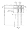
- FIG. 1 is a schematic plan view of a substrate cutting jig according to an embodiment.
- FIG. 2 is a partially enlarged view of FIG.
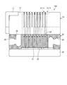
- FIG. 3 is a view taken in the direction of arrow A in FIG. 4 is a partial cross-sectional view taken along line BB of FIG.
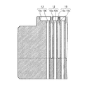
- FIG. 5 is a sectional view taken along the line CC of FIG.
- FIG. 6 is a schematic side view of a circuit board to be cut.
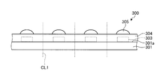
- FIG. 7 is a diagram showing an example in which an optoelectronic element is mounted on a circuit board.
- FIG. 8 is a diagram for explaining a substrate cutting method.
- FIG. 9 is a diagram illustrating a substrate cutting method.
- FIG. 10 is a diagram illustrating a substrate cutting method.
- FIG. 9 is a diagram illustrating a substrate cutting method.
- FIG. 11 is a diagram illustrating a substrate cutting method.
- FIG. 12A is a diagram illustrating a substrate cutting method.
- 12B is a diagram showing an electronic component obtained by dividing the circuit board shown in FIG.
- FIG. 13 is a view of inserting a wire into the laser beam receiving groove.
- FIG. 14A is a diagram showing another embodiment.
- FIG. 14B is a diagram showing another embodiment.
- FIG. 14C is a diagram showing another embodiment.
- FIG. 14D is a diagram showing another embodiment.
- FIG. 15 is a diagram illustrating a configuration in which an insertion material is interposed between the mounting surface and the circuit board.
- FIG. 16 is a diagram illustrating a configuration in which a holding jig for pressing the circuit board is provided.
- FIG. 16 is a diagram illustrating a configuration in which a holding jig for pressing the circuit board is provided.
- FIG. 17A is a diagram illustrating a manner of dividing the suction system.
- FIG. 17B is a diagram illustrating a manner of dividing the suction system.
- FIG. 17C is a diagram illustrating a manner of dividing the suction system.
- FIG. 17D is a diagram showing a manner of dividing the suction system.
- FIG. 18 is a cross-sectional view showing an example of the structure of the lower member when two suction systems are provided.
- FIG. 19 is a schematic side view of another aspect of the circuit board to be cut.
- FIG. 20 is a diagram for explaining a substrate cutting method.
- FIG. 21 is a diagram for explaining a substrate cutting method.
- FIG. 22 is a diagram for explaining a substrate cutting method.
- FIG. 23 is a diagram for explaining a substrate cutting method.
- FIG. 20 is a diagram for explaining a substrate cutting method.
- FIG. 24 is a diagram for explaining a substrate cutting method.
- FIG. 25 is a diagram for explaining a substrate cutting method.
- FIG. 26 is a diagram illustrating an individualized electronic component.
- FIG. 27A is a diagram for explaining the operation of a configuration in which a check valve is provided.
- FIG. 27B is a diagram for explaining the operation of the configuration provided with the check valve.
- FIG. 27C is a diagram for explaining the operation of the configuration in which the check valve is provided.
- FIG. 28A is a diagram for explaining the operation of another configuration in which a check valve is provided.
- FIG. 28B is a diagram illustrating the operation of another configuration in which a check valve is provided.
- FIG. 28C is a diagram illustrating the operation of another configuration in which a check valve is provided.
- FIG. 1 is a schematic plan view of a substrate cutting jig according to an embodiment of the present invention.
- FIG. 2 is a partially enlarged view of FIG.
- FIG. 3 is a view taken in the direction of arrow A in FIG. 4 is a partial cross-sectional view taken along line BB of FIG.
- FIG. 5 is a sectional view taken along the line CC of FIG.
- the substrate cutting jig 100 according to the present embodiment will be described with reference to FIGS.
- the substrate cutting jig 100 is made of an iron-based material such as steel, and includes a block-shaped upper member 10, a lower member 20, and a base 30 that are sequentially stacked.
- the substrate cutting jig 100 is not limited to an iron-based material such as steel, and may be composed of a material such as Al, Al alloy, Cu, Cu alloy, or ceramic.
- the lower member 20 and the base 30 are not directly irradiated with laser light, they can be made of resin, for example.
- the upper member 10 has a mounting surface 11, a plurality of substrate suction holes 12, 13, 14, a plurality of laser light receiving grooves 15, a plurality of dross suction holes 16, and a circuit board abutting member 17. ing.
- dross means a melted material in which the substrate is dissolved by the energy of the laser beam, which is generated when the substrate is cut by the laser beam.
- the lower member 20 includes a plurality of substrate suction holes 21, one substrate suction flow path 22, one substrate suction inlet 23, a plurality of dross suction grooves 24, one dross suction groove 25, 2 And two dross suction inlets 26.
- the mounting surface 11 is a surface for mounting a circuit board to be cut.
- the substrate suction holes 12, 13, 14 are formed on the placement surface 11 so as to penetrate the upper member 10.
- a total of 96 substrate suction holes 12 of 12 ⁇ 8 are arranged in a lattice pattern.
- the board suction holes 12 are formed in accordance with the number of protrusions and the arrangement pattern formed on the surface of the circuit board to be cut, which will be described later.
- a total of 40 substrate suction holes 13 are arranged at the outer peripheral side of the rectangle formed by the substrate suction holes 12, and only four substrate suction holes 14 are arranged at the corners. .
- the substrate suction hole 12 has a first inner diameter portion 12a and a second inner diameter portion 12b.
- the second inner diameter portion 12b communicates with the first inner diameter portion 12a and has an inner diameter smaller than the inner diameter of the first inner diameter portion 12a.
- the substrate suction holes 13 and 14 communicate with the first inner diameter portions 13a and 14a facing the placement surface 11 and the first inner diameter portions 13a and 14a, respectively, and from the inner diameter of the first inner diameter portions 13a and 14a.
- second inner diameter portions 13b and 14b each having a smaller inner diameter.
- a total of 22 laser light receiving grooves 15 are provided on the mounting surface 11 so as to extend between the lattices formed by the substrate suction holes 12, 13, and 14 and to cross each other.
- the laser beam receiving groove 15 communicates with the first groove width portion 15a facing the mounting surface 11 and the first groove width portion 15a, and the groove of the first groove width portion 15a.
- a second groove width portion 15b having a groove width wider than the width.
- the laser beam receiving groove 15 is formed so as to cross the upper member 10, and is opened on both side surfaces of the substrate cutting jig 100.
- the dross suction hole 16 communicates with the laser receiving groove 15 and is formed so as to penetrate the upper member 10. Further, a total of 117 dross suction holes 16 are provided at each intersection of the laser beam receiving grooves 15.
- the circuit board abutting member 17 is formed so as to protrude upward from the mounting surface 11 over the two sides of the upper member 10.
- each component of the lower member 20 will be described.
- a total of 140 substrate suction holes 21 are formed so as to communicate with the substrate suction holes 12, 13, and 14 of the upper member 10. Further, the substrate suction hole 21 communicates with one substrate suction flow path 22 formed by joining the lower member 20 and the base 30.
- the substrate suction channel 22 further communicates with a substrate suction inlet 23 formed on the side surface of the lower member 20.
- the dross suction grooves 24 extend in a lattice pattern below the dross suction holes 16 of the upper member 10, and one end of the dross suction groove 24 extending in the horizontal direction in FIG. 1 communicates with one dross suction groove 25. is doing.
- the dross suction groove 25 further communicates with two dross suction inlets 26 formed on the side surface of the lower member 20.
- the dross suction groove 24 may extend in a comb shape so as to communicate with the dross suction groove 25.
- the vertical relationship between the substrate suction flow path 22 and the dross suction groove 25 is not particularly limited to the present embodiment, and the substrate suction flow path 22 may be on the upper side.
- the circuit board to be cut will be described.
- the circuit board include those in which a chip of an electronic device or the like is mounted (attached) by die bonding or the like on a ceramic, resin, or metal substrate.
- FIG. 6 is a schematic side view of a circuit board to be cut.
- the circuit board 200 includes a substrate 201 having a front surface 201 a and a back surface 201 b, and a protrusion 202 formed on the front surface 201 a of the substrate 201.
- the substrate 201 includes a substrate made of ceramic such as alumina.
- the projecting portion 202 is, for example, an element mounted on the substrate 201 or an element in which a sealing resin is further formed on the element.
- a total of 96 protrusions 202 of 12 ⁇ 8 are arranged on the circuit board 200 in a lattice pattern.
- Examples of the circuit board 200 include those in which a large number of optoelectronic elements such as LED elements, chip capacitors, and ICs are mounted on a ceramic substrate to form a predetermined wiring pattern, or a resin encapsulated in a batch. You can apply the one that has stopped.
- FIG. 7 is a diagram showing an example in which an optoelectronic element is mounted on a circuit board.
- a large number of LED elements 303 are mounted on the surface 301 a of the substrate 301, and these are collectively sealed with a light-transmitting resin 304 such as silicone, and the LED elements 303 are also sealed.
- a resin is molded into the lens 305 by a mold.
- Reference sign CL1 is a planned cutting line.
- the lens 305 corresponds to the protrusion.
- the circuit board 200 is placed on the placement surface 11 of the substrate cutting jig 100 with the back surface 201b as the front side and the front surface 201a on which the protrusions 202 are formed as the back side. To do. At this time, by placing the circuit board 200 in contact with the circuit board abutting member 17, the circuit board 200 can be placed at an accurate position on the board cutting jig 100.
- the circuit board abutting member 17 is mounted so that the upper surface of the circuit board abutting member 17 is the same height as or lower than the upper surface of the circuit board 200 when the circuit board 200 is placed on the placement surface 11.
- the protrusion amount may be set so as to protrude from the placement surface 11.
- the substrate suction holes 12 are formed in accordance with the number of protrusions 202 and the arrangement pattern. Further, the first inner diameter portion 12a of the substrate suction hole 12 is formed in a size that can accommodate the protruding portion 202. As a result, when the circuit board 200 is placed, the protrusion 202 does not contact the board cutting jig 100. Thus, the substrate cutting jig 100 can place the circuit board 200 without being inclined with respect to the placement surface 11. Further, since the protrusion 202 does not come into contact with the substrate cutting jig 100 and is not damaged, it is particularly preferable when the protrusion 202 is an optical member such as a lens.
- a pipe 401 connected to a substrate suction device (not shown) having a vacuum pump is connected to the substrate suction inlet 23, and a vacuum pump is connected to the two dross suction inlets 26.
- a pipe 402 connected to a dross recovery apparatus (not shown) is connected.
- the substrate cutting device 500 sucks the circuit board 200 through the substrate suction holes 12, 13, 14, the substrate suction hole 21, the substrate suction channel 22, and the substrate suction inlet 23, and then the laser cutting device 500.
- the circuit board 200 is cut. Even if the circuit board 200 is warped or deformed due to this substrate adsorption, the circuit board 200 becomes flat, so that a satisfactory cutting can be performed.
- the board suction holes 13 and 14 face the outer peripheral side region of the circuit board 200. In this state, by suctioning from the second inner diameter portions 13b and 14b having a larger inner diameter, the outer peripheral side region of the circuit board 200 is more effectively adsorbed, and the circuit board 200 becomes flatter.
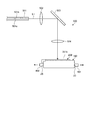
- a laser cutting device 500 that is a processing device includes a fiber laser 501 that is a laser light source, a collimator lens 502, a reflection mirror 503, and a condenser lens 504.
- the collimating lens 502, the reflecting mirror 503, and the condenser lens 504 constitute an optical system.
- the fiber laser 501 is a single mode optical fiber laser, and outputs a continuous laser beam L1 that is substantially a fundamental mode from an optical fiber having a core portion 501a and a cladding portion 501b.
- the laser beam L1 may be a multimode laser beam or a pulsed laser beam.
- the wavelength of the laser light L1 is, for example, 1064 nm to 1084 nm, and the optical output is, for example, 300 W to 500 W.
- the collimating lens 502 makes the laser light L1 parallel light.
- the reflection mirror 503 reflects the laser light L ⁇ b> 1 that is parallel light toward the circuit board 200.
- the condensing lens 504 condenses the reflected laser light L1 on the back surface 201b of the circuit board 200. That is, the optical system guides the laser beam L1 output from the fiber laser 501 to the circuit board 200 placed on the substrate cutting jig 100. Thereby, the circuit board 200 is cut by the heat generated by the conversion of the light energy of the laser light L1.
- the optical fiber of the fiber laser 501 and the collimating lens 502 are arranged directly above the substrate cutting jig 100, and the laser light L1 advances straight from top to bottom.
- the optical system may be configured as described above.
- the laser light L ⁇ b> 1 is condensed on the back surface 201 b of the circuit board 200 by the condenser lens 504.
- the circuit board 200 is cut by sweeping the laser light L1 along a predetermined sweep line on the circuit board 200, and the mounted elements are separated into predetermined electronic components.
- the laser light L1 may be swept by moving the irradiation position of the laser light L1 while the circuit board 200 is fixed, or the circuit board 200 is moved while the irradiation position of the laser light L1 is fixed. You may go in.
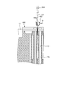
- the circuit board 200 is cut while blowing the assist gas G for blowing off the dross generated by the cutting from the gas nozzle 403.
- the laser beam L1 is applied to the circuit board 200 through the gas ejection holes 403a of the gas nozzle 403.
- the back surface 201 b of the circuit board 200 is the same height as the top surface of the circuit board abutting member 17 or higher than the top surface. This prevents the gas nozzle 403 from interfering with the circuit board abutting member 17.
- the gas nozzle 403 does not interfere with the protruding portion 202.
- the distance d between the gas ejection hole 403a of the gas nozzle 403 and the circuit board 200 can be reduced to about 0.5 mm or less, for example, and the effect of spraying the assist gas G is enhanced.
- the assist gas G is, for example, oxygen gas.
- the spray pressure of the assist gas G is 1.0 MPa, if the distance d is about 0.5 mm or less, the effect of blowing off the dross by the assist gas G is preferable.
- the laser beam L1 Since the laser beam L1 is irradiated from the back surface 201b side of the circuit board 200, the laser beam L1 directly reaches the substrate 201 to be cut. As a result, from the surface 201a side of the circuit board 200, the laser light L1 can reach the substrate 201 directly more directly than when the laser light L1 reaches the substrate 201 via, for example, a sealing resin, While being able to perform efficient cutting
- the laser receiving groove 15 is formed along the sweep line of the laser beam L1.
- the substrate cutting jig 100 receives the laser beam L1 that has passed through the cutting groove 203 formed in the circuit board 200 by the cutting by the laser receiving groove 15.
- the laser beam L1 reaches the mounting surface 11 of the substrate cutting jig 100 with a beam diameter close to the focused state, and the substrate cutting jig 100 is damaged. There is a fear.
- the laser receiving groove 15 receives the laser light L1.
- the beam diameter of the laser beam L1 is widened and the energy density is reduced. Damage is prevented.
- the laser beam receiving groove 15 has a depth at which the energy density of the laser beam L1 reaching the bottom surface 15c of the laser receiving groove 15 is such that the energy density does not damage the substrate cutting jig 100 and the width of the bottom surface 15c. Preferably it is formed.
- the substrate cutting jig 100 is made of an iron-based material and the wavelength of the laser beam L1 is 1084 nm
- the depth at which the energy density of the laser beam L1 reaching the bottom surface 15c is 10 4 W / cm 2 or less. It is preferable to make the thickness and width.
- the core diameter of the core portion 501a of the fiber laser 501 is about 11.6 ⁇ m
- NA is 0.073
- the output intensity of the laser beam L1 is 500 W
- the wavelength is 1084 nm
- the focal lengths of the collimating lens 502 and the condensing lens 504 are 100 mm.
- the beam diameter of the parallel light is about 14.6 mm
- the spot size of the laser light on the back surface 201b of the circuit board 200 is about 23 ⁇ m, for example.
- the light energy density at this time is about 10 8 W / cm 2 .
- the thickness of the substrate 201 is about 4.5 mm, the depth to the bottom surface 15c of the laser light receiving groove 15 is 20 mm, and the width at the bottom surface 15c is 1 mm, the energy density of the laser light L1 reaching the bottom surface 15c. Can be made 10 4 W / cm 2 or less.
- the laser beam L1 is also irradiated on the inner wall of the laser beam receiving groove 15, the energy density is lower than that of the bottom surface 15c because the laser beam L1 is irradiated with an inclination with respect to the inner wall.
- the focal length of the condensing lens 504 is preferably 80 mm to 200 mm in order to achieve a preferable focal depth that can secure the laser beam energy density necessary for cutting along the thickness direction of the circuit board 200.
- the depth to the bottom surface 15c of the laser beam receiving groove 15 is desirably about 15 mm to 40 mm depending on the focal length.
- the laser beam receiving groove 15 communicates with the first groove width portion 15a facing the placement surface 11 and the first groove width portion 15a, and has a groove width wider than the groove width of the first groove width portion 15a. And a second groove width portion 15b.
- the first groove width portion 15a facing the placement surface 11 the first groove width portion 15a and the first inner diameter portions 12a, 13a, and 14b of the substrate suction holes 12, 13, and 14
- the groove width of the second groove width portion 15b having the bottom surface 15c can be set with a high degree of freedom regardless of the groove width of the first groove width portion 15a.
- the dross D generated by the cutting is blown off by the assist gas G, and the dross collecting device communicates with the laser light receiving groove 15, the dross suction groove 24, the dross suction. It is sucked and collected through the groove 25 and the dross suction inlet 26.
- the dross suction hole 16 communicates with the laser beam receiving groove 15, the dross D generated by the cutting is quickly sucked and collected.
- the dross suction holes 16 are provided at the respective intersections of the laser light receiving grooves 15, the dross D can be sucked promptly regardless of which position of the circuit board 200 is cut.
- the dross D can be removed more quickly. Further, as shown in FIG. 3, since the laser light receiving groove 15 is open on both side surfaces of the substrate cutting jig 100, the assist gas G can blow through the laser light receiving groove 15, Removal is further promoted. As a result, since dross remains on the separated electronic component even when cutting at high speed, the efficiency is improved and the cutting quality is improved. In addition, a full cut that cuts the circuit board with one continuous laser beam irradiation allows slit processing to stop cutting within the substrate surface, and allows laser light to pass vertically or horizontally without stopping within the substrate surface. It is possible to freely cut and separate the substrate to separate the components.
- FIG. 12A is a diagram illustrating an electronic component obtained by separating the circuit board 300 illustrated in FIG. 7 as an example of the separated electronic component.
- a fiber laser that outputs a continuous laser beam having a wavelength of 1084 nm is used.
- the laser beam intensity is 300 W, 700 mm / sec, and 450 W Cutting at a very high speed of full cut of 1000 mm / sec can be realized.
- the substrate cutting jig 100 is prevented from being damaged by adjusting the depth and groove width of the laser beam receiving groove 15, but the substrate cutting jig 100 is formed by other methods. May prevent damage.
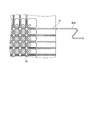
- a wire 405 as a wire made of metal for example, may be inserted into the laser light receiving groove 15 and disposed on the bottom surface.
- the wire 405 has a width or diameter smaller than the groove width of the laser beam receiving groove 15 and the inner diameter of the dross suction hole 16. If such a wire 405 is disposed on the bottom surface of the laser beam receiving groove 15 so that the wire 405 receives the laser beam L1, the risk of damage to the substrate cutting jig 100 is reduced.
- the wire 405 when the wire 405 is damaged by receiving the laser beam L1, it can be easily replaced, so that the running cost of the substrate cutting jig 100 can be reduced. Further, when the wire 405 is pulled upward, the wire 405 can be cleaned by scraping the dross on the inner wall of the laser beam receiving groove 15.
- the wires 405 are arranged so as to be installed at the bottoms of the respective laser light receiving grooves 15 corresponding to the arrangement of the plurality of laser light receiving grooves 15. You may use what combined in the mesh form. For example, if a part (wire replacement part) in which the wire 405 is stretched in a mesh shape is used inside the frame, the replacement of the wire is further facilitated.
- the wire 405 has a circular shape that is the simplest in cross-sectional shape, or a rectangular shape, a square shape, a (regular) polygonal shape such as a (regular) hexagonal shape or a (regular) triangle, and other ones such as a star shape.
- the cross-sectional shape having an acute angle at the portion may be a shape in which dross is easily scraped off at the corner of the cross-section.
- the wire 405 does not have to be straight in the longitudinal direction.
- the wire 405 may have a wavy shape in the longitudinal direction or a spiral shape like a spring. By doing so, the dross suction hole 16 is not easily blocked by the wire 405, and the scraping of the dross can be facilitated.
- the wire 405 is wavy in the longitudinal direction, the width of the wavy portion, and when the wire 405 is helical, the outer diameter of the spiral portion (the outer diameter of the spring-shaped portion) is By making it slightly larger than the groove width of the laser beam receiving groove 15, the dross can be more easily scraped.
- the laser beam L1 is irradiated by making the back surface 201b side of the circuit board 200 without the protrusion part 202 into the front side, this invention is not limited to this, The surface 201a of the circuit board 200 The laser beam L1 may be irradiated with the side as the front side.
- suction hole has the 1st internal diameter part and 2nd internal diameter part in which the internal diameter is changing discontinuously
- the shape of a hole is not specifically limited, For example, an internal diameter is depth.
- the first inner diameter portion and the second inner diameter portion may be realized by a hole having a tapered cross section that decreases in the direction.
- the effect of the present invention can be achieved by using a hole having a tapered cross section whose inner diameter expands in the depth direction, a hole having a constant inner diameter in the depth direction, and a straight section, or a combination thereof. Play.
- the shape of the hole for the laser beam receiving groove is not particularly limited, and the hole whose inner diameter is reduced or enlarged in the depth direction is tapered, the hole whose cross section is straight, or the like. The effects of the present invention are also obtained as a combination of the above.
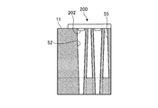
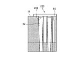
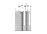
- FIGS. 14A to 14D are enlarged views of a cross section in the vicinity of the mounting surface 11 of the substrate cutting jig shown in FIG. 5, that is, a portion corresponding to the cross sectional view taken along the line CC of FIG. 2 in the above embodiment. Is. Similar to the above-described embodiment, the substrate 200 is placed so that the back surface is on the upper side and the protruding portion 202 does not contact the inner walls of the substrate suction holes 42, 52, 62, 72.
- FIG. 14A shows that the substrate suction hole 42 has a constant inner diameter and the laser light receiving groove 45 has a straight groove shape having a constant groove width.
- the size of the projecting portion 202 of the substrate 200 is small and the substrate suction hole and the laser beam receiving groove do not interfere with each other, at least one of the two may have a straight hole (groove) shape.
- the substrate suction hole 52 has a shape in which the inner diameter is reduced as it goes below the jig for cutting the substrate, whereas the laser light receiving groove 55 has a groove width as it goes below the jig.
- An enlarged shape for example, the substrate suction hole 52 is a substantially conical tapered hole and the laser beam receiving groove 55 is a groove having a tapered cross section (tapered groove)) is shown.
- both the substrate suction hole 52 and the laser beam receiving groove 55 may be tapered, thereby increasing the melt suction hole diameter of the laser beam receiving groove and increasing the suction amount.
- FIG. 14C shows a substrate suction hole 62 having a tapered hole shape and a laser beam receiving groove 65 having a straight groove with a constant width.
- FIG. 14D shows that the substrate suction hole 72 has a first inner diameter portion 72a and a second inner diameter portion 72b, but the laser light receiving groove 75 has a straight groove shape having a constant groove width.
- FIG. 15 is a diagram illustrating a configuration in which an insertion material 101 is interposed between the mounting surface 11 and the circuit board 200.
- the insertion material 101 is made of, for example, an adhesive material or an elastic material. If it is an adhesive material, it is suitable for supplementing adsorption of the circuit board 200 with the adhesive force and maintaining the airtightness between the mounting surface 11 and the circuit board 200. Further, the elastic material is also suitable for maintaining the airtightness between the mounting surface 11 and the circuit board 200.
- FIG. 16 is a diagram showing a configuration in which a holding jig for pressing the circuit board is provided.
- the holding jig 102 is disposed at a position shown in FIG. 16 and presses a circuit board (not shown) placed on the board cutting jig 100 from above. Since the holding jig 102 has a frame shape, the laser light is applied to the circuit board through the frame interior 102a.
- the holding jig 102 has an effect of preventing the electronic parts separated from the circuit board from being blown out by the assist gas. In addition, about the blow-off to the plane direction (surface direction of a mounting surface) of an electronic component, a blow-off is suppressed by adjacent electronic components separated.
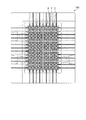
- FIGS. 17A to 17D are views showing a manner of dividing the suction system in the substrate cutting jig 100.
- the substrate suction holes are divided into two suction systems X and Y that are independent of each other.
- the suction system X and the suction system Y are alternately arranged one by one in both the vertical and horizontal directions on the paper.
- the suction system X and the suction system Y are arranged in a straight line in one direction (for example, the horizontal direction on the paper surface), and the suction system X and the suction system Y arranged in a straight line are alternately arranged. .
- the suction system X may surround the outer periphery of the suction system Y arranged in the grid
- the outer periphery of the circuit board can be strongly adsorbed by increasing the suction force of the suction system X.
- the substrate suction holes are divided into three suction systems X, suction systems Y, and suction systems Z that are independent from each other, and the suction systems X, Y are arranged one by one on the outer periphery of the suction system Z arranged in a lattice pattern. Surrounded by alternating arrangements.
- segmentation of a suction system is not restricted to these aspects, For example, the independent suction system may be used for every hole.
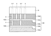
- FIG. 18 is a cross-sectional view showing an example of the structure of the lower member when two suction systems are provided.
- the lower member 120 is formed by stacking members 120a, 120b, and 120c.
- the cross section of the member 120a is a surface passing through the substrate suction hole of the suction system X
- the cross section of the member 120b is a surface passing through the substrate suction hole of the suction system Y.
- the substrate suction holes of the suction system X and the substrate suction holes of the suction system Y overlap in the depth direction of the page.
- a substrate suction flow path 122a communicating with the substrate suction inlet 123a is formed between the member 120a and the member 120b.
- the substrate adsorption flow path 122a communicates with the substrate suction holes of the suction system X.
- a substrate adsorption flow path 122b communicating with the substrate adsorption inlet 123b is formed between the member 120b and the member 120c.
- the substrate adsorption flow path 122b communicates with the substrate suction hole of the suction system Y.
- the circuit board to be cut by the board cutting jig according to the present invention is not limited to the one having the projecting portion like the circuit board 200.
- FIG. 19 is a schematic side view of another aspect of the circuit board to be cut.
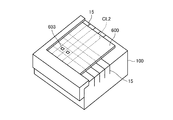
- the circuit board 600 includes a substrate 601 having a front surface 601a and a back surface 601b, a plurality of electronic elements 603 mounted on the front surface 601a of the substrate 601, and a resin 604 that collectively seals these electronic elements 603 with a resin.
- a resin 604 that collectively seals these electronic elements 603 with a resin.
- a light-transmitting material such as silicone or a non-light-transmitting material may be used depending on the type of the electronic element 603 and the like.
- Reference sign CL2 is a planned cutting line.
- the circuit board 600 When cutting the circuit board 600, first, as shown in FIG. 20, the circuit board 600 is used for cutting the board with the back surface 601b as the front side and the front surface 601a on which the electronic element 603 and the resin 604 are present as the back side. Place on the placement surface 11 of the jig 100. At this time, by placing the circuit board 600 in contact with the circuit board abutting member 17, the circuit board 600 can be placed at an accurate position on the board cutting jig 100.
- the circuit board 600 is placed on the mounting surface 11 of the substrate cutting jig 100 with the front surface 601a on which the electronic element 603 and the resin 604 are present as the front side and the back surface 601b as the back side. It may be placed.
- the first inner diameter portion 12a having a size that can accommodate the protruding portion is formed in the substrate suction hole 12 in both cases of FIGS. It does not have to be.
- the substrate suction hole 12 is formed with the inner diameter of the second inner diameter portion 12b having a small system, the contact area and the frictional force between the mounting surface 11 and the circuit board 600 are increased. As a result, it becomes difficult for the electronic parts separated after cutting to be misaligned. 6 and 8, when the circuit board 200 is placed on the placement surface 11 with the front surface 201a as the front side and the back surface 201b as the back side as shown in FIG.
- the first inner diameter portion 12a may not be formed.
- the first inner diameter portions 13a and 14a can be similarly omitted for the substrate suction holes 13 and 14.
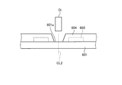
- the resin 604 is removed along the planned cutting line CL2 with a dicer Di or the like before the laser light irradiation, as shown in FIG. It is preferable to keep it.
- the laser beam L 1 output from the laser cutting device 500 is condensed on the circuit board 600 by the condenser lens 504.
- the circuit board 600 is cut so as to include the electronic elements 603 by sweeping the laser light L1 along a predetermined sweep line (scheduled cutting line CL2) on the circuit board 600. It is separated.
- the circuit board 600 is separated into electronic components each including a board 601, an electronic element 603, and a resin 604 as shown in FIG.
- the circuit board 600 is cut while spraying the assist gas G for blowing off the dross generated by the cutting from the gas nozzle 403.
- the laser beam L1 is applied to the circuit board 600 through the gas ejection hole 403a of the gas nozzle 403. Also in this case, the distance between the gas ejection hole 403a of the gas nozzle 403 and the circuit board 600 can be reduced to, for example, about 0.5 mm or less, and the effect of spraying the assist gas G is enhanced.
- the substrate suction hole 12 may be formed with the inner diameter of the second inner diameter portion 12b having a small diameter without forming the first inner diameter portion 12a having a size for accommodating the protruding portion. Good. It should be noted that the first inner diameter portions 13a and 14a can be similarly omitted for the substrate suction holes 13 and 14.
- each of the substrate suction holes may be provided with a mechanism for maintaining a vacuum degree independently.
- a mechanism for example, a check valve or a combination of a solenoid valve and a sensor can be used.
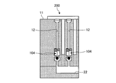
- FIGS. 27A to 27C are diagrams for explaining the operation of the configuration provided with the check valve.
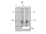
- a check valve 103 using a spring is provided below the substrate suction hole 12.
- the check valve 103 is opened. It becomes a state.
- the check valve 103 is closed as shown in FIG. 27B.
- the circuit board 200 is cut and the electronic components 204 are separated into individual pieces, it is assumed that one of the separated electronic components 204 is blown off as shown in FIG. 27C.
- the check valve 103 provided in the substrate suction hole 12 is opened and flows in.
- the air is exhausted from the substrate adsorption flow path 22.
- the check valve 103 provided in the other substrate suction hole 12 closed by the electronic component 204 is maintained in a closed state, the degree of vacuum in the substrate suction hole 12 is maintained, and the electronic component 204 is maintained. Adsorption is also maintained. Therefore, even if one electronic component 204 is blown away, a decrease in the overall adsorption force is prevented.
- This vacuum state can be released by a bypass provided separately. Accordingly, the suction of the electronic component 204 is also released, so that the electronic component 204 can be easily collected.
- FIG. 28A to 28C are diagrams for explaining the operation of another configuration provided with a check valve.
- a check valve 104 using a spring is provided below the substrate suction hole 12.
- the check valve 104 is opened. It becomes a state.
- the check valve 105 is closed as shown in FIG. 28B. After that, after the circuit board 200 is cut and the electronic component 204 is separated into pieces, it is assumed that one of the separated electronic components 204 is blown off as shown in FIG. 28C.
- the check valve 104 provided in the substrate suction hole 12 is opened and flows in.
- the air is exhausted from the substrate adsorption flow path 22.
- the check valve 104 provided in the other substrate suction hole 12 closed by the electronic component 204 is kept closed, the degree of vacuum in the substrate suction hole 12 is maintained, and the electronic component 204 Adsorption is also maintained. Therefore, even if one electronic component 204 is blown away, a decrease in the overall adsorption force is prevented.
- an electromagnetic valve (not shown) is provided below the substrate suction hole 12 and is controlled to open and close one by one or a plurality.
- a sensor (not shown) is arranged to monitor the pressure or air flow rate in the substrate suction hole 12 corresponding to the electromagnetic valve to be controlled. When the substrate is sucked, the electromagnetic valve is opened, and the airtight space constituted by the circuit board 200 and the substrate suction hole 12 is decompressed.
- a sensor that monitors the pressure or air flow rate of the released substrate suction hole 12 Detects an abnormality and closes the solenoid valve corresponding to the sensor.
- the substrate cutting jig, the processing apparatus, and the substrate cutting method according to the present invention are suitable mainly for use in laser processing.
Landscapes
- Engineering & Computer Science (AREA)
- Physics & Mathematics (AREA)
- Optics & Photonics (AREA)
- Mechanical Engineering (AREA)
- Plasma & Fusion (AREA)
- Manufacturing & Machinery (AREA)
- Microelectronics & Electronic Packaging (AREA)
- Laser Beam Processing (AREA)
- Auxiliary Devices For Machine Tools (AREA)
- Jigs For Machine Tools (AREA)
- Dicing (AREA)
Abstract
本願発明は、回路基板の切断の際に用いる基板切断用治具、加工装置及び切断方法に関し、より効率が良く、切断品質が高い基板切断を実現することを課題とし、複数の素子が実装された回路基板(200)が載置される載置面(11)に形成された、前記回路基板(200)を吸着するための複数の吸着孔(12,13)と、前記載置面(11)において、前記回路基板(200)を切断するために該回路基板(200)に照射されるレーザ光の掃引線に沿って形成された、前記レーザ光を受けるための複数のレーザ光受け溝(15)と、前記各レーザ受け溝(15)に連通するように形成された、前記回路基板(200)の切断によって発生する該回路基板(200)の溶解物を吸引するための吸引孔(16)と、を備える基板切断用治具(100)を使用する。
Description
本発明は、回路基板の切断の際に用いる基板切断用治具、加工装置および基板切断方法に関する。
電子部品、光電子部品等(以下、電子部品は電子部品および光電子部品を含むものとする)は、たとえばアルミナ(Al2O3)などからなるセラミック基板上に電子素子、光電子素子を多数実装して回路基板を作製し、この回路基板を切断して個々の素子を含む電子部品に個片化して製造される。近年、このような回路基板の切断方法として、レーザ光を用いた方法が開示されている(たとえば特許文献1参照)。レーザ光を用いて切断を行った場合、ダイサを用いた場合と比較して切断速度を早くすることができるので、より高い生産性が実現される。
レーザ光を用いた基板切断において、より効率が良く、切断品質が高い切断の実現が求められている。
本発明は、上記に鑑みてなされたものであって、レーザ光を用いて、より効率が良く、切断品質が高い基板切断を実現できる基板切断用治具、加工装置および基板切断方法を提供することを目的とする。
上述した課題を解決し、目的を達成するために、本発明に係る基板切断用治具は、複数の素子が実装された回路基板が載置される載置面に形成された、前記回路基板を吸着するための複数の吸着孔と、前記載置面において、前記回路基板を切断するために該回路基板に照射されるレーザ光の掃引線に沿って形成された、前記レーザ光を受けるための複数のレーザ光受け溝と、前記各レーザ受け溝に連通するように形成された、前記回路基板の切断によって発生する該回路基板の溶解物を吸引するための吸引孔と、を備えることを特徴とする。
また、本発明に係る基板切断用治具は、上記発明において、前記各吸着孔は、前記載置面に面する第1内径部と、前記第1内径部に連通し、前記第1内径部の内径よりも小さい内径を有する第2内径部とを有することを特徴とする。
また、本発明に係る基板切断用治具は、上記発明において、前記第1内径部は、前記回路基板の表面の突出部が収容される大きさに形成されていることを特徴とする。
また、本発明に係る基板切断用治具は、上記発明において、前記各レーザ光受け溝は、該レーザ受け溝の底面に到達する前記レーザ光のエネルギー密度が、当該基板切断用治具を損傷しない程度のエネルギー密度になる深さおよび前記底面の幅に形成されていることを特徴とする。
また、本発明に係る基板切断用治具は、上記発明において、前記各レーザ光受け溝は、該レーザ受け溝の底面に到達する前記レーザ光のエネルギー密度が、104W/cm2以下となる深さおよび前記底面の幅に形成されていることを特徴とする。
また、本発明に係る基板切断用治具は、上記発明において、前記各レーザ光受け溝は、前記載置面に面する第1溝幅部と、前記第1溝幅部に連通し、前記第1溝幅部の溝幅よりも広い溝幅を有する第2溝幅部とを有することを特徴とする。
また、本発明に係る基板切断用治具は、上記発明において、前記複数のレーザ光受け溝は互いに交差しており、前記吸引孔は前記レーザ受け溝の交差部に設けられていることを特徴とする。
また、本発明に係る基板切断用治具は、上記発明において、前記各レーザ光受け溝は、当該基板切断用治具の側面において開放されていることを特徴とする。
また、本発明に係る基板切断用治具は、上記発明において、前記各レーザ光受け溝の底面に、該各レーザ光受け溝の溝幅および前記吸引孔の内径よりも小さい幅の線材が配置されていることを特徴とする。
また、本発明に係る基板切断用治具は、上記発明において、前記複数の吸着孔は、異なる複数の吸引系統を有することを特徴とする。
また、本発明に係る基板切断用治具は、上記発明において、前記複数の吸着孔は、独立で真空度を保つ機構を備えることを特徴とする。
また、本発明に係る加工装置は、上記発明の基板切断用治具と、前記レーザ光を出力するレーザ光源と、を備えることを特徴とする。
また、本発明に係る基板切断方法は、複数の素子が実装された回路基板を治具の載置面に載置し、前記回路基板を前記治具の載置面に形成された複数の吸着孔から吸引して吸着しながら前記回路基板にレーザ光を照射して該回路基板を切断し、前記切断によって形成された切断溝から前記回路基板を通過した前記レーザ光を、前記治具の表面に形成されたレーザ光受け溝で受け、前記レーザ受け溝に連通する吸引孔から、前記切断によって発生した前記回路基板の溶解物を吸引する、ことを含むことを特徴とする。
また、本発明に係る基板切断方法は、上記発明において、前記レーザ光を照射した面側から前記切断した回路基板に粘着材を貼付し、前記切断によって個片化した部品を回収することを特徴とする。
本発明によれば、より効率が良く、切断品質が高い基板切断を実現できるという効果を奏する。
以下に、図面を参照して本発明に係る基板切断用治具、加工装置および基板切断方法の実施の形態を詳細に説明する。なお、この実施の形態によりこの発明が限定されるものではない。また、各図面において、同一または対応する要素には適宜同一の符号を付している。さらに、図面は模式的なものであり、各層の厚みと幅との関係、各層の比率などは、現実のものとは異なる場合があることに留意する必要がある。図面の相互間においても、互いの寸法の関係や比率が異なる部分が含まれている場合がある。
(実施の形態)
図1は、本発明の実施の形態に係る基板切断用治具の模式的な平面図である。図2は、図1の一部拡大図である。図3は、図1のA矢視図である。図4は、図3のB-B線一部断面図である。図5は、図2のC-C線要部断面図である。以下、図1~図5を用いて本実施の形態に係る基板切断用治具100について説明する。
図1は、本発明の実施の形態に係る基板切断用治具の模式的な平面図である。図2は、図1の一部拡大図である。図3は、図1のA矢視図である。図4は、図3のB-B線一部断面図である。図5は、図2のC-C線要部断面図である。以下、図1~図5を用いて本実施の形態に係る基板切断用治具100について説明する。
基板切断用治具100は、鋼等の鉄系の材料等からなり、順次積層された各々ブロック状の上部部材10と下部部材20と基台30とを備えている。なお、基板切断用治具100は、鋼等の鉄系の材料に限らず、Al、Al合金、Cu、Cu合金、あるいはセラミック等の材料で構成してもよい。また、下部部材20および基台30は直接レーザ光が照射されないので、例えば樹脂で構成することもできる。上部部材10は、載置面11と、複数の基板吸着孔12、13、14と、複数のレーザ光受け溝15と、複数のドロス吸引孔16と、回路基板突当部材17とを有している。ここで、ドロスとは、レーザ光によって基板を切断したときに発生する、レーザ光のエネルギーによって基板が溶解した溶解物を意味する。
下部部材20は、複数の基板吸着孔21と、1つの基板吸着用流路22と、1つの基板吸着用吸気口23と、複数のドロス吸引溝24と、1つのドロス吸引溝25と、2つのドロス吸引用吸気口26とを有している。
はじめに、上部部材10の各構成要素について説明する。まず、図1、図2に示すように、載置面11は、切断する回路基板を載置するための面である。基板吸着孔12、13、14は、載置面11に、上部部材10を貫通するように形成されている。基板吸着孔12は、12個×8個の合計96個が格子状に配列されている。基板吸着孔12は、後述する切断すべき回路基板の表面に形成された突出部の数および配列パターンに合わせて形成されている。基板吸着孔12の形成する長方形の外周の辺の部分には、合計で40個の基板吸着孔13が配置されており、角の部分には基板吸着孔14が合計4個だけ配置されている。
基板吸着孔12は、第1内径部12aと、第2内径部12bとを有する。第2内径部12bは、第1内径部12aに連通し、第1内径部12aの内径よりも小さい内径を有する。同様に、基板吸着孔13、14も、載置面11に面する第1内径部13a、14aと、第1内径部13a、14aのそれぞれに連通し、第1内径部13a、14aの内径よりも小さい内径を有する第2内径部13b、14bとをそれぞれ有する。
レーザ光受け溝15は、載置面11において、基板吸着孔12、13、14が形成する格子の間を延びるように、かつ互いに交差するように、合計で22本設けられている。図2、図3に示すように、レーザ光受け溝15は、載置面11に面する第1溝幅部15aと、第1溝幅部15aに連通し、第1溝幅部15aの溝幅よりも広い溝幅を有する第2溝幅部15bとを有する。また、図3に示すように、レーザ光受け溝15は、上部部材10を横断するように形成されており、基板切断用治具100の両側面において開放されている。
ドロス吸引孔16は、レーザ受け溝15に連通し、かつ上部部材10を貫通するように形成されている。また、ドロス吸引孔16は、レーザ光受け溝15の各交差部に、合計で117個だけ設けられている。
回路基板突当部材17は、上部部材10の二つの辺にわたって、載置面11から上側に突出するように形成されている。
つぎに、下部部材20の各構成要素について説明する。図4に示すように、基板吸着孔21は、上部部材10の基板吸着孔12、13、14のそれぞれに連通するように、合計140個形成されている。また、基板吸着孔21は、下部部材20と基台30とが接合することによって形成される1つの基板吸着用流路22に連通している。基板吸着用流路22はさらに下部部材20の側面に形成された基板吸着用吸気口23に連通している。
ドロス吸引溝24は、上部部材10のドロス吸引孔16の下方に格子状に延びており、かつ図1の紙面横方向に延びているドロス吸引溝24の一端は1つのドロス吸引溝25に連通している。ドロス吸引溝25はさらに下部部材20の側面に形成された2つのドロス吸引用吸気口26に連通している。なお、ドロス吸引溝24は、ドロス吸引溝25に連通するように櫛歯状に延びているものでも良い。また、基板吸着用流路22とドロス吸引溝25との上下関係は本実施の形態に特に限定されず、基板吸着用流路22が上であってもよい。
つぎに、基板切断用治具100を用いた基板切断方法について説明する。はじめに、切断すべき回路基板について説明する。回路基板としては、セラミック、樹脂、メタル等の基板に電子デバイスのチップ等がダイボンディング等により実装(取付)されたものが例示される。
図6は、切断すべき回路基板の模式的な側面図である。図6に示すように、回路基板200は、表面201aと裏面201bとを有する基板201と、基板201の表面201aに形成された突出部202とを備えている。
基板201は、たとえばアルミナなどのセラミックからなる基板を備えている。突出部202は、たとえば基板201に実装された素子や、素子の上にさらに封止用樹脂が形成されたもの等である。ここで、回路基板200には突出部202が12個×8個の合計96個が格子状に配列されているとする。
回路基板200の例としては、セラミック基板上にLED素子などの光電子素子やチップコンデンサやICなどの電子素子を多数実装し、所定の配線パターンを形成したものや、これにさらに一括して樹脂封止をしたものを適用することができる。
図7は、回路基板に光電子素子を実装した一例を示す図である。この回路基板300では、基板301の表面301aにLED素子303を多数実装し、これらを一括してシリコーン等の透光性の樹脂304で一括して樹脂封止するとともに、各LED素子303上の樹脂をモールドにてレンズ305に成型したものである。符号CL1は切断予定線である。レンズ305が突出部に対応する。
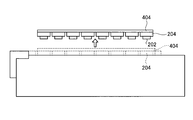
つぎに、図8~図12を用いて、回路基板200の切断方法について説明する。はじめに、図8に示すように、回路基板200を、裏面201bを表側とし、突出部202が形成された表面201aを裏側とした状態で、基板切断用治具100の載置面11に載置する。このとき、回路基板200を回路基板突当部材17に当接した状態で載置することによって、回路基板200を基板切断用治具100上の正確な位置に載置することができる。なお、回路基板突当部材17は、回路基板200を載置面11に載置した時に、回路基板突当部材17の上面が回路基板200上面と同じ高さか低い高さになる程度に、載置面11から突出するようにその突出量を設定するとよい。
また、上述したように、基板吸着孔12は、突出部202の数および配列パターンに合わせて形成されている。さらに、基板吸着孔12の第1内径部12aは、突出部202が収容される大きさに形成されている。その結果、回路基板200を載置したときに、突出部202が基板切断用治具100に接触しない。これによって、基板切断用治具100は、回路基板200を、載置面11に対して傾斜させることなく載置できる。また、突出部202が基板切断用治具100に接触してキズ等がつくことが無いので、突出部202がレンズなどの光学部材である場合に特に好ましい。
つぎに、図9に示すように、基板吸着用吸気口23に、真空ポンプを有する不図示の基板吸着装置に接続した配管401を接続し、2つのドロス吸引用吸気口26に、真空ポンプを有する不図示のドロス回収装置に接続した配管402を接続する。その後、基板吸着装置によって、基板吸着孔12、13、14、基板吸着孔21、基板吸着用流路22、基板吸着用吸気口23を介して、回路基板200を吸引しながら、レーザ切断装置500によって回路基板200の切断を行う。この基板吸着によって、回路基板200に反りや変形があったとしても、回路基板200は平坦になるので、良好な切断を行うことができる。また、回路基板200を載置面11に載置したとき、基板吸着孔13、14は、回路基板200の外周側領域に対向する。この状態で、より内径が大きい第2内径部13b、14bから吸引することによって、回路基板200の外周側領域がより効果的に吸着され、回路基板200はより平坦な状態となる。
加工装置であるレーザ切断装置500は、レーザ光源であるファイバレーザ501と、コリメートレンズ502と、反射ミラー503と、集光レンズ504とを備えている。また、コリメートレンズ502と、反射ミラー503と、集光レンズ504とで光学系を構成している。ファイバレーザ501は、シングルモード光ファイバレーザであり、コア部501aとクラッド部501bとを有する光ファイバから、実質的に基底モードである連続光のレーザ光L1を出力する。ただし、レーザ光L1はマルチモードレーザ光やパルスレーザ光でもよい。レーザ光L1の波長は、イッテルビウム添加光ファイバレーザの場合は、たとえば1064nm~1084nmであり、光出力はたとえば300W~500Wである。コリメートレンズ502は、レーザ光L1を平行光にする。反射ミラー503は、平行光とされたレーザ光L1を回路基板200に向けて反射させる。集光レンズ504は、反射されたレーザ光L1を回路基板200の裏面201bに集光させる。すなわち、光学系は、ファイバレーザ501から出力されたレーザ光L1を、基板切断用治具100に載置された回路基板200に導く。これによって、回路基板200はレーザ光L1の光エネルギーが変換して発生した熱によって切断される。
なお、レーザ切断装置500において、反射ミラー503は使わずに、ファイバレーザ501の光ファイバとコリメートレンズ502とを基板切断用治具100の真上に配置し、レーザ光L1が上から下に直進するように光学系を構成しても良い。
レーザ光L1による切断についてさらに具体的に説明する。図10に示すように、レーザ光L1は集光レンズ504によって回路基板200の裏面201bに集光される。そして、回路基板200上でレーザ光L1を所定の掃引線に沿って掃引することによって、回路基板200は切断され、実装された素子は所定の電子部品へと個片化される。なお、レーザ光L1の掃引は、回路基板200を固定したままレーザ光L1の照射位置を移動させることで行っても良いし、レーザ光L1の照射位置を固定したまま回路基板200を移動させることで行っても良い。
切断に際しては、ガスノズル403から、切断によって発生するドロスを吹き飛ばすためのアシストガスGを噴きつけながら回路基板200の切断を行う。レーザ光L1はガスノズル403のガス噴出孔403aを通して回路基板200に照射される。ここで、回路基板200の裏面201bは、回路基板突当部材17の上面と同じ高さあるいは上面よりも高くなる。これによって、ガスノズル403が回路基板突当部材17と干渉することがなくなる。
また、回路基板200の裏面201b側からレーザ光L1を照射するようにしているので、ガスノズル403が突出部202と干渉することがない。その結果、ガスノズル403のガス噴出孔403aと回路基板200との距離dを、たとえば0.5mm程度以下に近づけることができ、アシストガスGを噴きつける効果が高くなる。なお、アシストガスGはたとえば酸素ガスである。また、アシストガスGの噴きつけ圧を1.0MPaとした場合に、距離dを0.5mm程度以下とすれば、アシストガスGによるドロスを吹き飛ばす効果が高く好ましい。
また、回路基板200の裏面201b側からレーザ光L1を照射するようにしているので、レーザ光L1は直接、切断すべき基板201に到達することとなる。その結果、回路基板200の表面201a側から、レーザ光L1がたとえば封止樹脂を介して基板201に到達する場合よりも、より一層強い光エネルギーを基板201に直接的に到達させることができ、効率的な切断を行うことができるともに、封止樹脂の焼損、または熱によって溶解した樹脂が飛散したりすることを抑制できる。また、樹脂またはドロスなどが飛散して光学部材に付着するということも防止されるので好ましい。
ここで、レーザ受け溝15は、レーザ光L1の掃引線に沿って形成されている。これによって、基板切断用治具100は、切断によって回路基板200に形成された切断溝203を通過してきたレーザ光L1を、レーザ受け溝15で受けることとなる。レーザ受け溝15が無い場合は、レーザ光L1は、集光された状態に近いビーム径で基板切断用治具100の載置面11に到達することとなり、基板切断用治具100が損傷するおそれがある。これに対して、この基板切断用治具100では、レーザ受け溝15でレーザ光L1を受けるようにしている。その結果、レーザ光L1がレーザ受け溝15の内壁または底面に到達するときには、レーザ光L1のビーム径が広がり、そのエネルギー密度が低減された状態となっているので、基板切断用治具100の損傷は防止される。
したがって、レーザ光受け溝15は、レーザ受け溝15の底面15cに到達するレーザ光L1のエネルギー密度が、基板切断用治具100を損傷しない程度のエネルギー密度になる深さおよび底面15cの幅に形成されていることが好ましい。たとえば、基板切断用治具100が鉄系の材料からなり、レーザ光L1の波長が1084nmの場合、底面15cに達するレーザ光L1のエネルギー密度が、104W/cm2以下となるような深さおよび幅にすることが好ましい。
たとえば、ファイバレーザ501のコア部501aのコア径が約11.6μm、NAが0.073、レーザ光L1の出力強度が500W、波長が1084nm、コリメートレンズ502および集光レンズ504の焦点距離が100mm、平行光のビーム径が約14.6mmだとすると、回路基板200の裏面201b上でのレーザ光のスポットサイズはたとえば約23μmとなる。このときの光エネルギー密度は約108W/cm2である。このとき、基板201の厚さを約4.5mmとし、レーザ光受け溝15の底面15cまでの深さを20mm、底面15cでの幅を1mmとすると、底面15cに達するレーザ光L1のエネルギー密度を104W/cm2以下とすることができる。なお、レーザ光L1はレーザ光受け溝15の内側壁にも照射されるが、内側壁に対して傾斜して照射されるので、底面15cよりもエネルギー密度は低くなる。
集光レンズ504の焦点距離については、回路基板200の厚さ方向にわたって切断に必要なレーザ光エネルギー密度を確保できるような、好ましい焦点深度を実現するためには、80mm~200mmが好ましい。レーザ光受け溝15の底面15cまでの深さとしては、上記焦点距離に応じて15mm~40mm程度とすることが望ましい。
また、レーザ光受け溝15は、載置面11に面する第1溝幅部15aと、第1溝幅部15aに連通し、第1溝幅部15aの溝幅よりも広い溝幅を有する第2溝幅部15bとを有している。このように、載置面11に面する第1溝幅部15aを狭くすることによって、第1溝幅部15aと、基板吸着孔12、13、14の第1内径部12a、13a、14bとが干渉しないようにできるとともに、底面15cを有する第2溝幅部15bの溝幅を、第1溝幅部15aの溝幅にかかわらず自由度高く設定することができる。
さらに、図11に示すように、切断によって発生したドロスDは、アシストガスGによって吹き飛ばされるとともに、ドロス回収装置によって、レーザ光受け溝15に連通したドロス吸引孔16、ドロス吸引溝24、ドロス吸引溝25、ドロス吸引用吸気口26を介して吸引され、回収される。このように、ドロス吸引孔16がレーザ光受け溝15に連通していることによって、切断によって発生したドロスDは速やかに吸引、回収される。また、ドロス吸引孔16は、レーザ光受け溝15の各交差部に設けられているので、回路基板200のどの位置を切断していても、速やかにドロスDを吸引することができる。また、アシストガスGの噴きつけとドロスDの吸引とを併用することによって、より速やかにドロスDを除去することができる。さらに、図3に示すように、レーザ光受け溝15は基板切断用治具100の両側面において開放されているため、アシストガスGはレーザ光受け溝15を吹き抜けることができるので、ドロスDの除去がより促進される。その結果、高速で切断を行っても個片化した電子部品にドロスが残留することが抑制されるので、より効率が良く、切断品質が高くなる。また、一度の連続的なレーザ光照射で回路基板を切断するフルカットにより、基板面内で切断を停止するスリット加工や、レーザ光を基板面内で停止させず縦あるいは横方向に通過させて切断して、基板を切り離して部品を個片化させることを自由に行うことができる。
また、図12Aに示すように、切断によって個片化された電子部品204は、裏面側に粘着テープ等の粘着材404を貼付し、基板切断用治具100から引き上げることによって一度に効率良く回収することができる。このように、回路基板200の裏面201b側からレーザ光L1を照射して切断するようにしているので、切断後の電子部品204をより効率良く回収することができる。特に、電子部品204が光電子部品の場合は、これに含まれる光学部材にキズや汚れ等を付けることなく回収を行えるので特に好ましい。図12Bは、個片化された電子部品の例として図7に示す回路基板300を個片化した電子部品を示す図である。
以上説明したように、本実施の形態によれば、より効率が良く、切断品質が高い基板切断を実現できる。たとえば、厚さが0.4mmのアルミナ基板を切断する場合に、波長が1084nmの連続レーザ光を出力するファイバレーザを用いた場合、レーザ光強度が300Wの場合は700mm/sec、450Wの場合は1000mm/secという、きわめて高速なフルカットでの切断を実現できる。
なお、上記実施の形態では、レーザ光受け溝15の深さおよび溝幅を調整することによって、基板切断用治具100の損傷を防止しているが、他の方法によって基板切断用治具100の損傷を防止してもよい。たとえば、図13に示すように、レーザ光受け溝15にたとえば金属からなる線材としてのワイヤ405を挿入し、底面に配置してもよい。このワイヤ405は、レーザ光受け溝15の溝幅およびドロス吸引孔16の内径よりも小さい幅または直径とする。このようなワイヤ405をレーザ光受け溝15の底面に配置し、ワイヤ405がレーザ光L1を受けるようにすれば、基板切断用治具100の損傷のおそれが低減される。また、レーザ光L1を受けることによってワイヤ405が損傷した場合は容易に交換できるので、基板切断用治具100のランニングコストを低減できる。また、ワイヤ405を上方に引き上げるときに、ワイヤ405でレーザ光受け溝15の内壁のドロスを掻き出して、清掃することもできる。なお、ワイヤ405をレーザ光受け溝15の底面に配置するには、複数のレーザ光受け溝15の配置に対応して、各レーザ光受け溝15の底部に設置可能なように、ワイヤ405をメッシュ状に組み合わせたものを用いてもよい。たとえば、枠体の内部にワイヤ405をメッシュ状に張り巡らした部品(ワイヤ交換部品)を用いれば、ワイヤの交換がより一層容易である。
上記ワイヤ405は、断面形状として最も簡便な構造である円形のもの、あるいは長方形、正方形、(正)六角形や(正)三角形等の(正)多角形形状、その他例えば星型といったような一部に鋭角を有する断面形状として、断面の角部でドロスを掻き出しやすくした形状としてもよい。
また、上記ワイヤ405は、長手方向について真っ直ぐでなくても良く、例えば長手方向に波打ったような形状としたり、バネのようならせん状としても良い。このようにすることで、ドロス吸引孔16がワイヤ405によって塞がれ難くなるとともに、ドロスの掻き出しを容易にすることができる。なお、ワイヤ405が長手方向に波打った形状の場合は波打った部分の幅、ワイヤ405がらせん状の場合はらせん部の外径(バネ状となっている部分の外径)、がそれぞれレーザ光受け溝15の溝幅よりもわずかに大きくなるようにすることにより、ドロスを更に掻き出しやすくすることができる。
また、上記実施の形態では、突出部202が無い回路基板200の裏面201b側を表側として、レーザ光L1を照射するようにしているが、本発明はこれに限らず、回路基板200の表面201a側を表側として、レーザ光L1を照射するようにしてもよい。また、上記実施の形態では、基板吸着孔は、内径が不連続に変化している第1内径部と第2内径部とを有するが、孔の形状は特に限定されず、たとえば内径が深さ方向に向かって縮小するような、断面がテーパ形状の孔によって、第1内径部と第2内径部とを実現しても良い。または、内径が深さ方向に向かって拡大するような断面がテーパ形状の孔や、内径が深さ方向で一定である、断面がストレート形状の孔や、これらの組み合わせとしても本発明の効果を奏する。同様に、レーザ光受け溝についても、孔の形状は特に限定されず、内径が深さ方向に向かって縮小または拡大するような断面がテーパ形状の孔や、断面がストレート形状の孔や、これらの組み合わせとしても本発明の効果を奏する。
上記その他の実施の形態を、図14A~図14Dに示す。図14A~図14Dは、図5に示した基板切断用治具の載置面11近傍の断面、つまり上記実施の形態における図2のC-C線要部断面図に対応する部分を拡大したものである。基板200は、上記実施の形態と同様に、裏面側を上側にし、突出部202が基板吸引孔42、52、62、72の内壁に接触しないように載置されている。
図14Aは、基板吸引孔42が一定の内径を有し、レーザ光受け溝45が一定の溝幅を有するストレート溝形状であるものを示している。このように、基板200の突出部202のサイズが小さく、基板吸着孔、レーザ光受け溝が互いに干渉しない構造であれば、両者の少なくとも一方をストレート孔(溝)形状としてもよく、これにより基板切断用治具の構造をより簡便にするとともに、基板吸引用吸気量を増やすことができ、吸引力を増加させることができる。
図14Bは、基板吸引孔52が、基板切断用治具の下方に行くにつれて内径が縮小される形状とするのに対し、レーザ光受け溝55は、当該治具の下方に行くにつれ溝幅が拡大する形状(例えば、基板吸引孔52が略円錐状のテーパ孔であり、レーザ光受け溝55が断面テーパ形状の溝(テーパ溝))であるものを示している。このように、基板吸着孔52、レーザ光受け溝55ともにテーパ形状にしてもよく、これによりレーザ光受け溝の溶解物吸引孔径を大きくし、吸引量を増加させることができる。
図14Cは、基板吸着孔62をテーパ孔形状とし、レーザ光受け溝65を幅一定のストレート溝にしたものを示している。このようにすることで、突出部202のサイズが多少大きめであっても、基板吸着孔形状としては比較的簡便なものとし、当該治具全体として簡便な構造とすることができる。また、これとは逆に、基板吸着孔をストレート孔形状、レーザ光受け溝をテーパ溝形状としてもよい。このように、両者の孔(溝)形状は、上記各孔(溝)形状に伴う効果を奏するよう、適宜組み合わせることができる。
図14Dは、基板吸引孔72は第1内径部72aと第2内径部72bとを有するが、レーザ光受け溝75が一定の溝幅を有するストレート溝形状であるものを示している。
図15は、載置面11と回路基板200との間に介挿材101を介在させた構成を示す図である。図15では、一例として図14Dの構成を用いて説明しているが、他の構成に適用してもよい。介挿材101は、例えば粘着材や弾性材で構成される。粘着材であれば、その粘着力で回路基板200の吸着を補い、載置面11と回路基板200との間の気密性を保つのに好適である。また、弾性材の場合も、載置面11と回路基板200との間の気密性を保つのに好適である。
図16は、回路基板を押える押さえ治具を設けた構成を示す図である。押え治具102は、図16に示す位置に配置され、基板切断用治具100に載置された不図示の回路基板を上から押えつける。なお、押え治具102は枠状の形状を有しているので、レーザ光は枠内部102aを通して回路基板に照射される。
押え治具102は、回路基板から個片化された電子部品のアシストガスによる吹き飛びを防止する効果を奏する。なお、電子部品の平面方向(載置面の面方向)への吹き飛びについては、隣接する個片化した電子部品同士によって吹き飛びが抑制される。
なお、或る個片化した電子部品が吹き飛ぶと、そこから基板吸引孔に空気が流入し、回路基板全体の吸着力が低下する場合がある。そこで、基板切断用治具における吸引系統を互いに独立した複数の吸引系統に分割し、電子部品が吹き飛んだ場合でも吸着力低下を抑制できる構成とすることが好ましい。
図17A~図17Dは、基板切断用治具100における吸引系統の分割の態様を示す図である。図17A~図17Dでは、基板吸着孔が互いに独立した吸引系統Xと吸引系統Yとに2分割している。図17Aでは、吸引系統Xと吸引系統Yとが紙面縦、横方向の両方について1つずつ交互に配置されている。図17Bでは、吸引系統Xと吸引系統Yとは、それぞれ一方向(たとえば紙面横方向)に直線状に配列しつつ、その直線配列した吸引系統Xと吸引系統Yとが交互に配置されている。図17Cでは、格子状に配列した吸引系統Yの外周を吸引系統Xが取り囲むように配置されている。図17Cでは吸引系統Xの吸引力を強くすることによって回路基板の外周を強力に吸着することができる。図17Dでは、基板吸着孔が互いに独立した吸引系統Xと吸引系統Yと吸引系統Zとに3分割しており、格子状に配列した吸引系統Zの外周を吸引系統X、Yが1つずつ交互に配置されて取り囲んでいる。なお、吸引系統の分割の態様はこれらの態様に限られず、たとえば1孔ごとに独立した吸引系統が使用されていてもよい。
図18は、2つの吸引系統を設ける場合の下部部材の構造の一例を示す断面図である。図18では、下部部材120は部材120a、120b、120cが積層して構成されている。部材120aの断面は吸引系統Xの基板吸引孔を通る面であり、部材120bの断面は吸引系統Yの基板吸引孔を通る面である。なお、紙面左側から1番目、3番目の基板吸引孔については、吸引系統Xの基板吸引孔と吸引系統Yの基板吸引孔とが紙面の奥行き方向に重なっている。
部材120aと部材120bとの間には、基板吸着用吸気口123aに連通する基板吸着用流路122aが形成される。基板吸着用流路122aは吸引系統Xの基板吸引孔に連通している。部材120bと部材120cとの間には、基板吸着用吸気口123bに連通する基板吸着用流路122bが形成される。基板吸着用流路122bは吸引系統Yの基板吸引孔に連通している。このように、下部部材120を積層構造とすることによって吸引系統を複数の独立した吸引系統とすることができる。
ところで、本発明に係る基板切断用治具で切断する回路基板については、回路基板200のように突出部があるものに限られない。
図19は、切断すべき回路基板の別の態様の模式的な側面図である。回路基板600は、表面601aと裏面601bとを有する基板601と、基板601の表面601aに多数実装された電子素子603と、これらの電子素子603を一括して樹脂封止する樹脂604とで構成されている。樹脂604としては電子素子603の種類等の必要に応じて、シリコーン等の透光性のもの、または非透光性のものを使用してもよい。符号CL2は切断予定線である。
回路基板600を切断する場合は、まず、図20に示すように、回路基板600を、裏面601bを表側とし、電子素子603および樹脂604が存在する表面601aを裏側とした状態で、基板切断用治具100の載置面11に載置する。このとき、回路基板600を回路基板突当部材17に当接した状態で載置することによって、回路基板600を基板切断用治具100上の正確な位置に載置することができる。
また、回路基板600は、図21に示すように、電子素子603および樹脂604が存在する表面601aを表側とし、裏面601bを裏側とした状態で、基板切断用治具100の載置面11に載置してもよい。
ここで、回路基板600には突出部が無いので、図20、21の場合のいずれにおいても、基板吸着孔12については、突出部が収容される大きさの第1内径部12aは形成されていなくてもよい。この場合、基板吸着孔12は、系が小さい第2内径部12bの内径で形成されるため、載置面11と回路基板600との接触面積および摩擦力が大きくなる。その結果、切断後に個片化した電子部品が位置ズレしにくくなる。なお、図6、8に示す回路基板200についても、図22に示すように表面201aを表側とし、裏面201bを裏側とした状態で載置面11に載置する場合は、基板吸着孔12の第1内径部12aは形成されていなくてもよい。なお、基板吸着孔13、14についても、第1内径部13a、14aを同様に省略することができる。
図21のように樹脂604側が表になるように回路基板600を載置する場合は、図23に示すように、レーザ光照射前にダイサDi等で切断予定線CL2に沿って樹脂604を除去しておくことが好ましい。図22に示す場合も同様である。
なお、図8、20のように回路基板200や回路基板600の裏面を表側として載置する場合でも、樹脂304や樹脂604をあらかじめ除去しておくと、レーザ光の照射によって溶融した樹脂が飛散したり、封止樹脂が焼損したりすることがないので好ましい。
なお、図8、20のように回路基板200や回路基板600の裏面を表側として載置する場合でも、樹脂304や樹脂604をあらかじめ除去しておくと、レーザ光の照射によって溶融した樹脂が飛散したり、封止樹脂が焼損したりすることがないので好ましい。
つぎに、図24に示すように、レーザ切断装置500が出力したレーザ光L1を集光レンズ504によって回路基板600に集光する。そして、図25に示すように回路基板600上でレーザ光L1を所定の掃引線(切断予定線CL2)に沿って掃引することによって、回路基板600はそれぞれ電子素子603を含むように切断、個片化される。これによって、回路基板600は、図26に示すような基板601と電子素子603と樹脂604とで構成される電子部品へと個片化される。
切断に際しては、ガスノズル403から、切断によって発生するドロスを吹き飛ばすためのアシストガスGを噴きつけながら回路基板600の切断を行う。レーザ光L1はガスノズル403のガス噴出孔403aを通して回路基板600に照射される。この場合も、ガスノズル403のガス噴出孔403aと回路基板600との距離を、たとえば0.5mm程度以下に近づけることができ、アシストガスGを噴きつける効果が高くなる。
なお、図24に示すように、基板吸着孔12は、突出部が収容される大きさの第1内径部12aは形成されずに、径が小さい第2内径部12bの内径で形成されてもよい。なお、基板吸着孔13、14についても、第1内径部13a、14aを同様に省略することができる。
ところで上述したように、或る個片化した電子部品が吹き飛ぶと、そこから空気が流入し、同一の吸引系統あるいは回路基板全体の吸着力が低下する場合がある。これを防止するために、基板吸着孔のそれぞれが独立で真空度を保つ機構を備えていてもよい。このような機構としては、たとえば逆止弁や、電磁弁とセンサーを組み合わせた構成を利用できる。
図27A~図27Cは、逆止弁を設けた構成の動作を説明する図である。ばねを用いた逆止弁103は基板吸着孔12の下方に設けられている。まず、図27Aに示すように、載置面11に載置された回路基板200が基板吸着孔12と基板吸着用流路22とを介して吸引されているときは、逆止弁103が開状態となる。つぎに、基板吸着孔12内の真空度が高まると、図27Bに示すように逆止弁103は閉状態となる。その後、回路基板200を切断して電子部品204を個片化した後に、図27Cに示すように個片化された電子部品204の一つが吹き飛ばされたとする。このとき、吹き飛ばされた電子部品204によって閉ざされていた基板吸着孔12が外気に開放され、空気が流入すると、その基板吸着孔12内に設けられた逆止弁103が開状態となり、流入した空気は基板吸着用流路22から排気される。しかし、電子部品204によって閉ざされている他の基板吸着孔12内に設けられた逆止弁103は閉状態に維持されるので、その基板吸着孔12内の真空度は維持され、電子部品204の吸着も維持される。したがって、1個の電子部品204が吹き飛ばされても、全体の吸着力の低下が防止される。なお、この真空状態は別途設けられたバイパスによって解除することができる。これによって、電子部品204の吸着も解除されるので、電子部品204を容易に回収することができる。
図28A~図28Cは、逆止弁を設けた他の構成の動作を説明する図である。ばねを用いた逆止弁104は基板吸着孔12の下方に設けられている。まず、図28Aに示すように、載置面11に載置された回路基板200が基板吸着孔12と基板吸着用流路22とを介して吸引されているときは、逆止弁104が開状態となる。つぎに、基板吸着孔12内の真空度が高まると、図28Bに示すように逆止弁105は閉状態となる。その後、回路基板200を切断して電子部品204を個片化した後に、図28Cに示すように個片化された電子部品204の一つが吹き飛ばされたとする。このとき、吹き飛ばされた電子部品204によって閉ざされていた基板吸着孔12が外気に開放され、空気が流入すると、その基板吸着孔12内に設けられた逆止弁104が開状態となり、流入した空気は基板吸着用流路22から排気される。しかし、電子部品204によって閉ざされている他の基板吸着孔12内に設けられた逆止弁104は閉状態に維持されるので、基板吸着孔12内の真空度は維持され、電子部品204の吸着も維持される。したがって、1個の電子部品204が吹き飛ばされても、全体の吸着力の低下が防止される。
電磁弁とセンサーを組み合わせた構成としては、たとえば次のようなものがある。まず、基板吸着孔12の下方に図示しない電磁弁が設けられ、1つずつあるいは複数をセットとして開閉制御される。また、図示しないセンサーは、制御する電磁弁に対応して基板吸着孔12内の圧力あるいは空気流量をモニタするように配置される。そして、基板を吸引する時は電磁弁が開状態として、回路基板200と基板吸着孔12で構成される気密空間が減圧される。ここで、基板切断時に、吹き飛ばされた電子部品204によって閉ざされていた基板吸着孔12が外気に開放され空気が流入すると、解放された基板吸着孔12の圧力あるいは空気流量をモニタしているセンサーが異常を検知し、当該センサーに対応する電磁弁を閉状態とする。このようにすることで、開放状態となった基板吸着孔12の真空状態を維持し、その他の基板吸着孔12の吸引力低下を防止することができる。
なお、上記実施の形態により本発明が限定されるものではない。上述した各構成要素を適宜組み合わせて構成したものも本発明に含まれる。また、さらなる効果や変形例は、当業者によって容易に導き出すことができる。よって、本発明のより広範な態様は、上記の実施の形態に限定されるものではなく、様々な変更が可能である。
以上のように、本発明に係る基板切断用治具、加工装置および基板切断方法は、主にレーザ加工の用途に利用して好適なものである。
10 上部部材
11 載置面
12、13、14、42、52、62、72 基板吸着孔
12a、13a、14a、72a 第1内径部
12b、13b、14b、72b 第2内径部
15、45、55,65、75 レーザ光受け溝
15a 第1溝幅部
15b 第2溝幅部
15c 底面
16 ドロス吸引孔
17 回路基板突当部材
20、120 下部部材
21 基板吸着孔
22、122a、122b 基板吸着用流路
23、123a、123b 基板吸着用吸気口
24、25 ドロス吸引溝
26 ドロス吸引用吸気口
30 基台
502 コリメートレンズ
100 基板切断用治具
101 介挿材
102 押え治具
102a 枠内部
103、104 逆止弁
120a、120b、120c 部材
200、300、600 回路基板
201、301、601 基板
201a、301a、601a 表面
201b、601b 裏面
202 突出部
203 切断溝
204 電子部品
303 LED素子
304、604 樹脂
305 レンズ
401、402 配管
403 ガスノズル
403a ガス噴出孔
404 粘着材
405 ワイヤ
500 レーザ切断装置
501 ファイバレーザ
501a コア部
501b クラッド部
502 コリメートレンズ
503 反射ミラー
504 集光レンズ
603 電子素子
d 距離
D ドロス
Di ダイサ
G アシストガス
L1 レーザ光
X、Y、Z 吸引系統
11 載置面
12、13、14、42、52、62、72 基板吸着孔
12a、13a、14a、72a 第1内径部
12b、13b、14b、72b 第2内径部
15、45、55,65、75 レーザ光受け溝
15a 第1溝幅部
15b 第2溝幅部
15c 底面
16 ドロス吸引孔
17 回路基板突当部材
20、120 下部部材
21 基板吸着孔
22、122a、122b 基板吸着用流路
23、123a、123b 基板吸着用吸気口
24、25 ドロス吸引溝
26 ドロス吸引用吸気口
30 基台
502 コリメートレンズ
100 基板切断用治具
101 介挿材
102 押え治具
102a 枠内部
103、104 逆止弁
120a、120b、120c 部材
200、300、600 回路基板
201、301、601 基板
201a、301a、601a 表面
201b、601b 裏面
202 突出部
203 切断溝
204 電子部品
303 LED素子
304、604 樹脂
305 レンズ
401、402 配管
403 ガスノズル
403a ガス噴出孔
404 粘着材
405 ワイヤ
500 レーザ切断装置
501 ファイバレーザ
501a コア部
501b クラッド部
502 コリメートレンズ
503 反射ミラー
504 集光レンズ
603 電子素子
d 距離
D ドロス
Di ダイサ
G アシストガス
L1 レーザ光
X、Y、Z 吸引系統
Claims (14)
- 複数の素子が実装された回路基板が載置される載置面に形成された、前記回路基板を吸着するための複数の吸着孔と、
前記載置面において、前記回路基板を切断するために該回路基板に照射されるレーザ光の掃引線に沿って形成された、前記レーザ光を受けるための複数のレーザ光受け溝と、
前記各レーザ受け溝に連通するように形成された、前記回路基板の切断によって発生する該回路基板の溶解物を吸引するための吸引孔と、
を備えることを特徴とする基板切断用治具。 - 前記各吸着孔は、前記載置面に面する第1内径部と、前記第1内径部に連通し、前記第1内径部の内径よりも小さい内径を有する第2内径部とを有することを特徴とする請求項1に記載の基板切断用治具。
- 前記第1内径部は、前記回路基板の表面の突出部が収容される大きさに形成されていることを特徴とする請求項2に記載の基板切断用治具。
- 前記各レーザ光受け溝は、該レーザ受け溝の底面に到達する前記レーザ光のエネルギー密度が、当該基板切断用治具を損傷しない程度のエネルギー密度になる深さおよび前記底面の幅に形成されていることを特徴とする請求項1~3のいずれか一つに記載の基板切断用治具。
- 前記各レーザ光受け溝は、該レーザ受け溝の底面に到達する前記レーザ光のエネルギー密度が、104W/cm2以下となる深さおよび前記底面の幅に形成されていることを特徴とする請求項4に記載の基板切断用治具。
- 前記各レーザ光受け溝は、前記載置面に面する第1溝幅部と、前記第1溝幅部に連通し、前記第1溝幅部の溝幅よりも広い溝幅を有する第2溝幅部とを有することを特徴とする請求項1~5のいずれか一つに記載の基板切断用治具。
- 前記複数のレーザ光受け溝は互いに交差しており、前記吸引孔は前記レーザ受け溝の交差部に設けられていることを特徴とする請求項1~6のいずれか一つに記載の基板切断用治具。
- 前記各レーザ光受け溝は、当該基板切断用治具の側面において開放されていることを特徴とする請求項1~7のいずれか一つに記載の基板切断用治具。
- 前記各レーザ光受け溝の底面に、該各レーザ光受け溝の溝幅および前記吸引孔の内径よりも小さい幅の線材が配置されていることを特徴とする請求項1~8のいずれか一つに記載の基板切断用治具。
- 前記複数の吸着孔は、異なる複数の吸引系統を有することを特徴とする請求項1~9のいずれか一つに記載の基板切断用治具。
- 前記複数の吸着孔は、独立で真空度を保つ機構を備えることを特徴とする請求項1~10のいずれか一つに記載の基板切断用治具。
- 請求項1~11のいずれか一つに記載の基板切断用治具と、
前記レーザ光を出力するレーザ光源と、
を備えることを特徴とする加工装置。 - 複数の素子が実装された回路基板を治具の載置面に載置し、
前記回路基板を前記治具の載置面に形成された複数の吸着孔から吸引して吸着しながら前記回路基板にレーザ光を照射して該回路基板を切断し、
前記切断によって形成された切断溝から前記回路基板を通過した前記レーザ光を、前記治具の表面に形成されたレーザ光受け溝で受け、
前記レーザ受け溝に連通する吸引孔から、前記切断によって発生した前記回路基板の溶解物を吸引する、
ことを含むことを特徴とする基板切断方法。 - 前記レーザ光を照射した面側から前記切断した回路基板に粘着材を貼付し、前記切断によって個片化した部品を回収することを特徴とする請求項13に記載の基板切断方法。
Priority Applications (1)
| Application Number | Priority Date | Filing Date | Title |
|---|---|---|---|
| JP2013551868A JP6082702B2 (ja) | 2011-12-28 | 2012-12-28 | 基板切断用治具、加工装置および基板切断方法 |
Applications Claiming Priority (2)
| Application Number | Priority Date | Filing Date | Title |
|---|---|---|---|
| JP2011289830 | 2011-12-28 | ||
| JP2011-289830 | 2011-12-28 |
Publications (1)
| Publication Number | Publication Date |
|---|---|
| WO2013100149A1 true WO2013100149A1 (ja) | 2013-07-04 |
Family
ID=48697626
Family Applications (1)
| Application Number | Title | Priority Date | Filing Date |
|---|---|---|---|
| PCT/JP2012/084217 Ceased WO2013100149A1 (ja) | 2011-12-28 | 2012-12-28 | 基板切断用治具、加工装置および基板切断方法 |
Country Status (2)
| Country | Link |
|---|---|
| JP (1) | JP6082702B2 (ja) |
| WO (1) | WO2013100149A1 (ja) |
Cited By (11)
| Publication number | Priority date | Publication date | Assignee | Title |
|---|---|---|---|---|
| CN103639602A (zh) * | 2013-12-09 | 2014-03-19 | 南京中科煜宸激光技术有限公司 | 一种薄板激光焊接装夹系统 |
| JP2015085345A (ja) * | 2013-10-29 | 2015-05-07 | 株式会社ディスコ | レーザー加工装置 |
| JP2016025112A (ja) * | 2014-07-16 | 2016-02-08 | 株式会社ディスコ | レーザー切断方法及びレーザー加工装置 |
| WO2018168002A1 (ja) * | 2017-03-16 | 2018-09-20 | 株式会社日本製鋼所 | レーザ照射装置、レーザ照射方法、及び半導体装置の製造方法 |
| US10239161B2 (en) | 2015-10-29 | 2019-03-26 | Samsung Display Co., Ltd. | Stage for cutting substrate and substrate-cutting apparatus |
| CN110860811A (zh) * | 2019-11-29 | 2020-03-06 | 上海精测半导体技术有限公司 | 一种激光切割载台 |
| CN111822869A (zh) * | 2019-04-18 | 2020-10-27 | 三星显示有限公司 | 基板切割台及包括基板切割台的基板切割设备 |
| JP2020534670A (ja) * | 2017-09-13 | 2020-11-26 | ジェニュイン ソリューションズ ピーティーイー リミテッド | ポリマー樹脂モールド化合物ベースの基板の切断方法およびそのシステム |
| JP2021077904A (ja) * | 2021-01-21 | 2021-05-20 | 株式会社日本製鋼所 | レーザ照射装置 |
| KR20210094681A (ko) * | 2020-01-21 | 2021-07-30 | 삼성디스플레이 주식회사 | 레이저 장치 및 이를 이용한 표시 장치의 제조 방법 |
| JP2023084205A (ja) * | 2021-12-07 | 2023-06-19 | 古河電気工業株式会社 | 端子配置台及び端子配置方法 |
Citations (9)
| Publication number | Priority date | Publication date | Assignee | Title |
|---|---|---|---|---|
| JPH04139786A (ja) * | 1990-09-29 | 1992-05-13 | Ibiden Co Ltd | 電子部品搭載用基板の外形加工装置 |
| JP2001053443A (ja) * | 1999-08-06 | 2001-02-23 | Hitachi Ltd | 電子回路基板の製造方法,電子回路基板の製造装置及び電子回路基板 |
| JP2001347433A (ja) * | 2000-06-07 | 2001-12-18 | Hitachi Ltd | 吸着システム |
| JP2002324768A (ja) * | 2001-02-21 | 2002-11-08 | Nec Machinery Corp | 基板切断方法 |
| JP2003002677A (ja) * | 2001-06-22 | 2003-01-08 | Seiko Epson Corp | レーザ割断用支持テーブル、レーザ割断装置、レーザ割断方法、及び、液晶パネルの製造方法 |
| JP2007090508A (ja) * | 2005-09-30 | 2007-04-12 | Disco Abrasive Syst Ltd | メモリーカード基板の分割方法 |
| JP2007320124A (ja) * | 2006-05-31 | 2007-12-13 | Sharp Corp | 被加工脆性板の切断装置および切断方法 |
| JP2008137016A (ja) * | 2006-11-30 | 2008-06-19 | Renesas Technology Corp | 半導体装置の製造方法 |
| JP2008229682A (ja) * | 2007-03-22 | 2008-10-02 | Epson Toyocom Corp | パッケージ部品の製造方法 |
Family Cites Families (5)
| Publication number | Priority date | Publication date | Assignee | Title |
|---|---|---|---|---|
| JPS6010639A (ja) * | 1983-06-29 | 1985-01-19 | Toshiba Corp | ウエ−ハ着脱装置 |
| JPH0499047A (ja) * | 1990-08-07 | 1992-03-31 | Meidensha Corp | 半導体製造方法 |
| JP2001267271A (ja) * | 2000-03-22 | 2001-09-28 | Yoshioka Seiko:Kk | 吸着装置 |
| JP3945331B2 (ja) * | 2002-07-17 | 2007-07-18 | 松下電器産業株式会社 | 半導体チップのピックアップ装置および吸着剥離ツール |
| JP2004186635A (ja) * | 2002-12-06 | 2004-07-02 | Sharp Corp | 半導体基板の切断装置および切断方法 |
-
2012
- 2012-12-28 WO PCT/JP2012/084217 patent/WO2013100149A1/ja not_active Ceased
- 2012-12-28 JP JP2013551868A patent/JP6082702B2/ja active Active
Patent Citations (9)
| Publication number | Priority date | Publication date | Assignee | Title |
|---|---|---|---|---|
| JPH04139786A (ja) * | 1990-09-29 | 1992-05-13 | Ibiden Co Ltd | 電子部品搭載用基板の外形加工装置 |
| JP2001053443A (ja) * | 1999-08-06 | 2001-02-23 | Hitachi Ltd | 電子回路基板の製造方法,電子回路基板の製造装置及び電子回路基板 |
| JP2001347433A (ja) * | 2000-06-07 | 2001-12-18 | Hitachi Ltd | 吸着システム |
| JP2002324768A (ja) * | 2001-02-21 | 2002-11-08 | Nec Machinery Corp | 基板切断方法 |
| JP2003002677A (ja) * | 2001-06-22 | 2003-01-08 | Seiko Epson Corp | レーザ割断用支持テーブル、レーザ割断装置、レーザ割断方法、及び、液晶パネルの製造方法 |
| JP2007090508A (ja) * | 2005-09-30 | 2007-04-12 | Disco Abrasive Syst Ltd | メモリーカード基板の分割方法 |
| JP2007320124A (ja) * | 2006-05-31 | 2007-12-13 | Sharp Corp | 被加工脆性板の切断装置および切断方法 |
| JP2008137016A (ja) * | 2006-11-30 | 2008-06-19 | Renesas Technology Corp | 半導体装置の製造方法 |
| JP2008229682A (ja) * | 2007-03-22 | 2008-10-02 | Epson Toyocom Corp | パッケージ部品の製造方法 |
Cited By (21)
| Publication number | Priority date | Publication date | Assignee | Title |
|---|---|---|---|---|
| JP2015085345A (ja) * | 2013-10-29 | 2015-05-07 | 株式会社ディスコ | レーザー加工装置 |
| CN103639602A (zh) * | 2013-12-09 | 2014-03-19 | 南京中科煜宸激光技术有限公司 | 一种薄板激光焊接装夹系统 |
| JP2016025112A (ja) * | 2014-07-16 | 2016-02-08 | 株式会社ディスコ | レーザー切断方法及びレーザー加工装置 |
| US10239161B2 (en) | 2015-10-29 | 2019-03-26 | Samsung Display Co., Ltd. | Stage for cutting substrate and substrate-cutting apparatus |
| US10950474B2 (en) | 2017-03-16 | 2021-03-16 | The Japan Steel Works, Ltd. | Laser irradiation apparatus, laser irradiation method, and method for manufacturing semiconductor device |
| CN114393295A (zh) * | 2017-03-16 | 2022-04-26 | 株式会社日本制钢所 | 激光照射装置 |
| CN110418691A (zh) * | 2017-03-16 | 2019-11-05 | 株式会社日本制钢所 | 激光照射装置、激光照射方法以及半导体器件制造方法 |
| WO2018168002A1 (ja) * | 2017-03-16 | 2018-09-20 | 株式会社日本製鋼所 | レーザ照射装置、レーザ照射方法、及び半導体装置の製造方法 |
| US11676831B2 (en) | 2017-03-16 | 2023-06-13 | Jsw Aktina System Co., Ltd | Laser irradiation apparatus, laser irradiation method, and method for manufacturing semiconductor device |
| JP2018157000A (ja) * | 2017-03-16 | 2018-10-04 | 株式会社日本製鋼所 | レーザ照射装置、レーザ照射方法、及び半導体装置の製造方法 |
| CN110418691B (zh) * | 2017-03-16 | 2022-02-15 | 株式会社日本制钢所 | 激光照射装置、激光照射方法以及半导体器件制造方法 |
| JP2020534670A (ja) * | 2017-09-13 | 2020-11-26 | ジェニュイン ソリューションズ ピーティーイー リミテッド | ポリマー樹脂モールド化合物ベースの基板の切断方法およびそのシステム |
| EP3668677A4 (en) * | 2017-09-13 | 2021-06-23 | Genuine Solutions Pte. Ltd. | CUTTING PROCESS FOR SUBSTRATES ON THE BASIS OF A POLYMER RESIN MOLD COMPOUND AND A SYSTEM FOR IT |
| JP7012824B2 (ja) | 2017-09-13 | 2022-01-28 | ジェニュイン ソリューションズ ピーティーイー リミテッド | ポリマー樹脂モールド化合物ベースの基板の切断方法およびそのシステム |
| CN111822869A (zh) * | 2019-04-18 | 2020-10-27 | 三星显示有限公司 | 基板切割台及包括基板切割台的基板切割设备 |
| CN110860811A (zh) * | 2019-11-29 | 2020-03-06 | 上海精测半导体技术有限公司 | 一种激光切割载台 |
| KR20210094681A (ko) * | 2020-01-21 | 2021-07-30 | 삼성디스플레이 주식회사 | 레이저 장치 및 이를 이용한 표시 장치의 제조 방법 |
| KR102750609B1 (ko) | 2020-01-21 | 2025-01-09 | 삼성디스플레이 주식회사 | 레이저 장치 및 이를 이용한 표시 장치의 제조 방법 |
| JP7159363B2 (ja) | 2021-01-21 | 2022-10-24 | Jswアクティナシステム株式会社 | レーザ照射装置 |
| JP2021077904A (ja) * | 2021-01-21 | 2021-05-20 | 株式会社日本製鋼所 | レーザ照射装置 |
| JP2023084205A (ja) * | 2021-12-07 | 2023-06-19 | 古河電気工業株式会社 | 端子配置台及び端子配置方法 |
Also Published As
| Publication number | Publication date |
|---|---|
| JPWO2013100149A1 (ja) | 2015-05-11 |
| JP6082702B2 (ja) | 2017-02-15 |
Similar Documents
| Publication | Publication Date | Title |
|---|---|---|
| JP6082702B2 (ja) | 基板切断用治具、加工装置および基板切断方法 | |
| CN102481666B (zh) | 激光加工方法及芯片 | |
| JP5162163B2 (ja) | ウェーハのレーザ加工方法 | |
| US8652860B2 (en) | Packaging photon building blocks having only top side connections in a molded interconnect structure | |
| CN109719390B (zh) | 激光加工设备 | |
| KR102155917B1 (ko) | 광 디바이스 | |
| SG188829A1 (en) | Semiconductor cutting device, semiconductor cutting method, semiconductor cutting system, laser cutting device and laser cutting method | |
| JP5261168B2 (ja) | 電子部品製造用の切断装置及び切断方法 | |
| US20200343405A1 (en) | Optical device layer transferring method | |
| TWI582865B (zh) | 接合裝置 | |
| KR20150089931A (ko) | 광디바이스 및 광디바이스의 가공 방법 | |
| JP2011026177A (ja) | 加工対象物切断方法 | |
| KR20120135097A (ko) | 반도체 발광 소자, 그 제조 방법, 이를 포함하는 반도체 발광 소자 패키지 및 레이저 가공 장치 | |
| JP7431601B2 (ja) | レーザー加工装置 | |
| EP2810308A1 (en) | Packaging photon building blocks having only top side connections in a molded interconnect structure | |
| CN104795478A (zh) | 光器件及光器件的加工方法 | |
| JP2006245062A (ja) | Iii族窒化物系化合物半導体素子の製造方法及び発光素子 | |
| JP2016143735A (ja) | 発光装置の製造方法 | |
| TW201509577A (zh) | 光裝置及光裝置之加工方法 | |
| WO2006038713A1 (en) | Production method for semiconductor device | |
| CN111195776B (zh) | 用于切割衬底的台和衬底切割装置 | |
| JP6090277B2 (ja) | 発光モジュール | |
| JP7617770B2 (ja) | 洗浄装置、洗浄方法、および、半導体装置の製造方法 | |
| CN106133919B (zh) | 晶元级光学组件及其制造方法 | |
| KR100596022B1 (ko) | 디스펜서 스테이지의 글라스 흡착구조 |
Legal Events
| Date | Code | Title | Description |
|---|---|---|---|
| 121 | Ep: the epo has been informed by wipo that ep was designated in this application |
Ref document number: 12863922 Country of ref document: EP Kind code of ref document: A1 |
|
| ENP | Entry into the national phase |
Ref document number: 2013551868 Country of ref document: JP Kind code of ref document: A |
|
| NENP | Non-entry into the national phase |
Ref country code: DE |
|
| 122 | Ep: pct application non-entry in european phase |
Ref document number: 12863922 Country of ref document: EP Kind code of ref document: A1 |