WO2013099760A1 - 光源装置、および、フィラメント - Google Patents
光源装置、および、フィラメント Download PDFInfo
- Publication number
- WO2013099760A1 WO2013099760A1 PCT/JP2012/083089 JP2012083089W WO2013099760A1 WO 2013099760 A1 WO2013099760 A1 WO 2013099760A1 JP 2012083089 W JP2012083089 W JP 2012083089W WO 2013099760 A1 WO2013099760 A1 WO 2013099760A1
- Authority
- WO
- WIPO (PCT)
- Prior art keywords
- filament
- light
- source device
- light source
- visible light
- Prior art date
- Legal status (The legal status is an assumption and is not a legal conclusion. Google has not performed a legal analysis and makes no representation as to the accuracy of the status listed.)
- Ceased
Links
Images


Classifications
-
- H—ELECTRICITY
- H01—ELECTRIC ELEMENTS
- H01K—ELECTRIC INCANDESCENT LAMPS
- H01K1/00—Details
- H01K1/26—Screens; Filters
-
- H—ELECTRICITY
- H01—ELECTRIC ELEMENTS
- H01K—ELECTRIC INCANDESCENT LAMPS
- H01K1/00—Details
- H01K1/02—Incandescent bodies
- H01K1/04—Incandescent bodies characterised by the material thereof
- H01K1/10—Bodies of metal or carbon combined with other substance
-
- H—ELECTRICITY
- H01—ELECTRIC ELEMENTS
- H01K—ELECTRIC INCANDESCENT LAMPS
- H01K1/00—Details
- H01K1/62—One or more circuit elements structurally associated with the lamp
-
- H—ELECTRICITY
- H01—ELECTRIC ELEMENTS
- H01K—ELECTRIC INCANDESCENT LAMPS
- H01K3/00—Apparatus or processes adapted to the manufacture, installing, removal, or maintenance of incandescent lamps or parts thereof
- H01K3/02—Manufacture of incandescent bodies
Definitions
- the present invention relates to a light source filament with improved energy utilization efficiency, and more particularly to a light source device using the filament, particularly an incandescent bulb, a near infrared light source, and a thermionic emission source.
- Incandescent light bulbs are widely used that emit light by flowing current through a tungsten filament or the like.
- An incandescent bulb has a radiation spectrum with excellent color rendering properties close to that of sunlight, and the conversion efficiency from the power of the incandescent bulb to light is 80% or more, but the wavelength component of the emitted light is as shown in FIG.
- the infrared radiation component is 90% or more (in the case of 3000K in FIG. 1).
- the conversion efficiency from the electric power of the incandescent bulb to visible light is as low as about 15 lm / W.
- the fluorescent lamp has a conversion efficiency from electric power to visible light of about 90 lm / W, which is larger than the incandescent bulb.
- the incandescent bulb is excellent in color rendering, but has a larger environmental load than the fluorescent lamp.
- Patent Documents 1 and 2 have a configuration in which an inert gas or a halogen gas is sealed inside a light bulb, whereby the evaporated filament material is halogenated and returned to the filament (halogen cycle) to increase the filament temperature. Proposed. These are generally called halogen lamps. Thereby, the effect of the increase in the power conversion efficiency to visible light and the extension of a filament lifetime is acquired. In this configuration, it is important to control the components of the sealed gas and the pressure in order to increase the efficiency and extend the life.
- Patent Documents 3-5 disclose a configuration in which an infrared reflecting coating is applied to the surface of a bulb glass so that infrared light emitted from the filament is reflected, returned to the filament, and absorbed. High efficiency is achieved by reheating the filament with infrared light reabsorbed by the filament.
- Patent Documents 6 to 9 propose a configuration in which a fine structure is produced in the filament itself, and the infrared radiation is suppressed and the ratio of visible light radiation is increased by the physical effect of the fine structure.
- JP-A-60-253146 Japanese Patent Laid-Open No. 62-10854 JP 59-58752 A JP-T 62-501109 JP 2000-123795 A JP 2001-519079 Japanese Patent Laid-Open No. 6-5263 JP-A-6-2167 JP 2006-205332 A
- Patent Documents 1 and 2 can achieve a life extension effect, but it is difficult to greatly improve the conversion efficiency, and the current efficiency is about 20 lm / W. is there.
- the technique of reflecting infrared radiation with an infrared reflecting coat and reabsorbing the filament is efficient because the reflectance of infrared light by the filament is as high as 70%. It does n’t happen well. Further, the infrared light reflected by the infrared reflective coating is absorbed by other parts other than the filament, such as the filament holding part and the base, and is not used for heating the filament. For this reason, it is difficult to greatly improve the conversion efficiency by this technology. Currently, the efficiency is about 20 lm / W.
- a technique for suppressing infrared radiation with a fine structure as in Patent Documents 6-9 is a report showing a radiation enhancement and suppression effect with respect to the wavelength of the extreme part of the infrared radiation spectrum as in Non-Patent Document 1.
- a fine microfabrication technique such as electron beam lithography is used for producing a fine structure, a light source using this is very expensive.
- the fine structure portion is melted and destroyed at a heating temperature of about 1000 ° C.
- An object of the present invention is to provide a light source device including a filament with high efficiency for converting electric power into visible light.
- a light source device provided by the present invention includes a translucent airtight container, a filament disposed in the translucent airtight container, and a lead wire for supplying a current to the filament.
- the filament has a base made of a metal material and a white scatterer layer covering the base. A visible light absorbing material that absorbs light in the visible light region is added to the white scatterer layer.
- the infrared light radiation can be suppressed and the visible light radiation can be enhanced by the filament having a high reflectance in the infrared wavelength region and a low reflectance in the visible light wavelength region, the visible light luminous efficiency is improved.
- a light source device having a high level can be obtained.
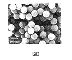
- the graph which shows the wavelength dependence characteristic of the radiation energy of the conventional tungsten filament The scanning electron micrograph which shows the particle shape of the white scatterer (lutetia) of this embodiment.
- the graph which shows the infrared reflection spectrum before and after giving a dangling bond and a surface crystal defect recovery process to a white scatterer.
- the graph which shows the wavelength dependence characteristic of the reflectance and the radiation efficiency of the filament which coat
- the present invention relates to a light source device having a translucent airtight container, a filament disposed in the translucent airtight container, and a lead wire for supplying a current to the filament.
- the filament has a base made of a metal material and a white scatterer layer that covers the base, and a visible light absorber that absorbs light in the visible light region is added to the white scatterer layer.
- the reflectance of the filament can be increased in a wide wavelength range including the infrared light region, and the reflectance in the visible light region can be decreased.
- visible light can be emitted with high efficiency.
- the filament has a base made of a metal material and a light reflection layer that covers the base and has a higher reflectance of infrared light than the base. It contains a reflectance lowering material that lowers the reflectance in the visible light region of the light scatterer.
- the light reflection layer can be formed of a white scatterer to which a visible light absorbing material that absorbs light in the visible light region is added as a reflectance lowering material.
- the substrate of the filament is a metal having a high melting point, for example, HfC (melting point 4160K), TaC (melting point 4150K), ZrC (melting point 3810K), C (melting point 3800K), W (melting point 3680K), Re (melting point 3453K), Os. (Melting point 3327K), Ta (melting point 3269K), Mo (melting point 2890K), Nb (melting point 2741K), Ir (melting point 2683K), Ru (melting point 2583K), Rh (melting point 2239K), V (melting point 2160K), Cr (melting point) 2130K) and Zr (melting point 2125K).
- HfC melting point 4160K
- TaC melting point 4150K
- ZrC melting point 3810K
- C melting point 3800K
- W melting point 3680K
- Re melting point 3453K
- Os. Melting point 3327K
- white scatterer examples include yttria (Y 2 O 3 ), hafnia (HfO 2 ), lutecia (Lu 2 O 3 ), tria (ThO 2 ), magnesia (MgO), zirconia (ZrO 2 ), ytterbia (Yb 2 O 3 ), strontia (SrO), calcium oxide (CaO), beryllium oxide (BeO), holmium oxide (Ho 2 O 3 ), zirconia nitride (ZrN), titanium nitride (TiN), and boron nitride (BN) The thing containing either of these is used.
- the white scatterer has heat resistance and maintains high reflection characteristics even in a temperature range of 2300 K or more where the filament emits light efficiently.
- the particles of the white scatterer desirably have a particle size of 50 nm or more and 50 ⁇ m or less.
- the shape of the particles is preferably a shape that allows a large filling rate in terms of light scattering efficiency. Considering the coating method on the substrate, it is desirable that the spherical particles have good symmetry.
- the white scatterer is more preferably subjected to at least one of a surface dangling bond removal treatment and a surface crystal defect recovery treatment.
- an impurity element doped in a white scatterer can be used.
- the impurity element Ce, Eu, Mn, Ti, Sn, Tb, Au, Ag, Cu, Al, Ni, W, Pb, As, Tm, Ho, Er, Dy, Pr, or the like can be used.
- the doping concentration of the impurity element into the white scatterer is set to 0.0001% to 10%, for example.
- a doping method a method in which a white scatterer and these impurity elements are mixed and doped using a solid-phase reaction (firing), or a white scatterer oxide and an impurity are both dissolved in concentrated nitric acid. A method of co-precipitation with an acid salt and firing it can be used.
- metal particles as the visible light absorbing material.
- the metal particles include W, Ta, Mo, Au, Ag, Cu, Al, Ti, Ni, Co, Cr, Si, V, Mn, Fe, Nb, Ru, Pt, Pd, Hf, Y, Particles such as Zr, Re, Os, and Ir can be used.
- the particle size of the metal particles is preferably 2 nm or more and 5 ⁇ m or less.
- the concentration of the metal particles added to the white scatterer is set to 0.0001% to 10%, for example.
- a white scatterer and these impurity elements are mixed and electrodeposited, and then fired to grow a crystal of metal fine particles in the white scatterer, or the above metal ions are added to the white scatterer.
- the metal particles added to the white scatterer form various absorption bands because the absorption wavelength and the amount of absorption in the visible light region can be controlled according to the type and particle size of the metal, as in the stained glass of a church. It becomes possible. For example, by changing the particle size of Au fine particles from 2 nm to 5 nm, the stained glass color can be changed from pink to deep green.
- the filament base is preferably polished to a mirror surface.
- the reflectance of infrared light having a wavelength of 4000 nm or more is preferably 90% or more. It is preferable that the reflectance of infrared light having a shorter wavelength, for example, infrared light at a wavelength of 1000 nm or more is 90% or more, since further improvement in luminous efficiency can be expected.
- the surface roughness of the substrate preferably satisfies at least one of a center line average roughness Ra of 1 ⁇ m or less, a maximum height Rmax of 10 ⁇ m or less, and a ten-point average roughness Rz of 10 ⁇ m or less.
- the filament for light source of the present invention emits visible light with high efficiency when the filament is heated by current supply or the like. The principle will be described below based on Kirchhoff's law in blackbody radiation.
- P (total) is the total input energy
- P (conduction) is the energy lost through the lead that supplies current to the filament
- P (radiation) is the temperature at which the filament is heated. It is the energy lost by radiating light.
- the temperature of the filament reaches 2300K or higher, the energy lost through the lead wire is only about 5%, and the remaining 95% or more energy is lost to the outside by light radiation.
- Almost all of the input power can be converted to light.
- the proportion of the visible light component is only about 10% as shown in FIG. 1, and most of it is the infrared radiated light component. Then, it is not an efficient visible light source.
- Equation (2) the term of P (radiation) in the above formula (1) can be described by the following formula (2).
- ⁇ ( ⁇ ) represents the emissivity at each wavelength
- ⁇ ⁇ 5 / (exp ( ⁇ / ⁇ T) ⁇ 1) represents Planck's radiation law.
- ⁇ 3.747 ⁇ 10 8 W ⁇ m 4 / m 2
- ⁇ 1.4387 ⁇ 10 4 ⁇ mK.
- ⁇ ( ⁇ ) has a relationship of the reflectance R ( ⁇ ) and the equation (3) according to Kirchhoff's law.
- the reflectivity is very high (that is, the emissivity is very low from the infrared light region to the visible light region).
- a device to reduce the reflectance in the visible light region in order to improve the radiation efficiency in the visible light region while suppressing the radiation in the infrared light region, and to make the filament with good visible light luminous efficiency, a device to reduce the reflectance in the visible light region (increase the emissivity) (See formula (3)).
- a technique of adding impurities used in phosphor technology or adding metal fine particles to the white scatterer is used. Thereby, an absorption band is generated in the visible light region in the white scatterer, and a filament with high visible light luminous flux efficiency can be realized.
- the following method can be used as a method of coating the filament base with the white scatterer layer to which impurities are added.
- white scatterer particles for example, lutecia (Lu 2 O 3 )
- spherical lutetia (Lu 2 O 3 ) particles having a particle size of 50 nm to 50 ⁇ m are prepared as an example as shown in a scanning electron micrograph in FIG.
- This white scatterer is doped with Ce at a concentration of 1% by the solid phase reaction method.
- nitrocellulose as a binder is mixed with the white scatterer and dispersed in a mixed solution of water and polyvinyl alcohol to form a slurry.
- the slurry-like white scatterer is applied around a filament substrate (for example, W (tungsten)) having a desired shape (for example, a wire) prepared separately, and then is applied at a predetermined temperature, for example, 400 ° C. or more. And firing in an oxidizing atmosphere. Thereby, the binder is burned out and the filament can be covered with the white scatterer layer doped with impurities.
- the white scatterer particles can be accelerated and collided, and the filament can be covered with the white scatterer layer doped with impurities by the impact sinter coating method in which the sinter coating can be instantaneously applied by the impact. Can do.
- the surface roughness satisfies at least one of a center line average roughness Ra of 1 ⁇ m or less, a maximum height Rmax of 10 ⁇ m or less, and a ten-point average roughness Rz of 10 ⁇ m or less.
- a mirror-polished W filament ( ⁇ 2 mm wire) was produced.
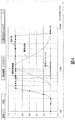
- the reflectance of the mirror-polished W filament and the wavelength dependence characteristic (radiation spectrum) of the radiation efficiency exhibited when the filament was heated to 2500 K were determined by simulation and experiment. The result is shown in FIG.
- the visible light luminous efficiency of this W filament is 16.9 lm / W.
- FIG. 4 shows the reflectivity and emissivity (2500 K) of a filament coated with a white scatterer (Lu 2 O 3 ) layer not doped with impurities or metal particles on the mirror-polished W filament (substrate) of FIG.
- required the wavelength dependence characteristic of this by simulation and experiment is shown.
- this filament has an extremely high reflectance of almost 1 in the ultraviolet light region, visible light region, and infrared light region due to the action of the white scatterer layer, and the emissivity is almost 0. It is. For this reason, the visible light luminous efficiency of the filament of FIG. 4 is a low value of 3.1 lm / W.
- FIG. 4 shows the reflectivity and emissivity (2500 K) of a filament coated with a white scatterer (Lu 2 O 3 ) layer not doped with impurities or metal particles on the mirror-polished W filament (substrate) of FIG.
- the visible light luminous efficiency of the filament of FIG. 4 is a low value
- the low reflectance portion of the infrared region in the ultraviolet region and the wavelength of 7 ⁇ m or more are the conduction band energy absorption (ultraviolet region) of Lu 2 O 3 white body and the optical phonon of Lu 2 O 3 , respectively. This is due to absorption (infrared part: 1TO phonon, 1LO phonon, 2TO phonon, 2LO phonon, etc.).
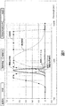
- the mirror-polished W filament (substrate) of FIG. 3 is coated with a white scatterer layer in which white impurities (Lu 2 O 3 ) are doped with about 1% of Ce impurities, with a thickness of 100 ⁇ m.
- white impurities Li 2 O 3
- Ce impurities doped with about 1% of Ce impurities, with a thickness of 100 ⁇ m.
- required the wavelength dependence characteristic of the reflectance of the filament of this invention and the wavelength dependence characteristic (radiation spectrum) of radiation efficiency (2500K) by simulation and experiment is shown.
- a band where the reflectance is close to zero is generated in the visible light region centered around the peak 550 nm of the visibility curve. Thereby, radiation efficiency is increasing in the visible light region.
- the filament of the present invention has a very high visible light luminous flux efficiency of 133.5 lm / W. This visible light luminous efficiency is approximately 10 times that of conventional incandescent bulbs.
- OH groups water adsorbed on the surface and crystal defects (dangling bonds) on the surface create a large absorption in the infrared region as shown in FIG. If pulled, it causes a decrease in luminous efficiency of visible light. Therefore, it is desirable to perform a process for removing OH groups and crystal defects from the surface of the white scatterer.
- the treatment method of removing OH groups and crystal defects can be used widely known process known as (reference:.. M. Hudicky et al, Chemistry of Organic Fluorine Compounds, 2 nd ed Ellis Horwood Ltd 1976).
- a method in which white scatterer particles are washed with NH 4 F (buffered hydrofluoric acid) or the like and H in the OH group is replaced with F can be used. Thereafter, when baking is performed at a high temperature of 1000 ° C. or higher in a vacuum or an oxidizing atmosphere, OF groups are removed and crystal defects are recovered. By performing a series of these operations, the reflectance can be gradually improved as shown in FIG. In addition, the dashed-dotted line in FIG. 6 shows the infrared reflection spectrum of the white scatterer particle
- the non-treated filament shown in FIG. 5 can increase the reflectance of the infrared region of 99% to 99.9%. it can.
- FIG. 7 shows the wavelength dependence characteristic of the reflectance and the wavelength dependence characteristic (radiation spectrum) of the radiation efficiency of the filament formed in the same manner as the filament of FIG.
- the visible light beam efficiency at 2500 K of the filament of FIG. 7 is obtained, it is 168.7 lm / W, and it can be seen that the visible light beam efficiency of the filament of FIG. 5 can be greatly increased from 133.5 lm / W.
- the thickness of the white scatterer layer to which the impurity dope or the metal particles are added in consideration of the following points. That is, by covering with the white scatterer layer, the surface area S of the filament is increased more than the surface area of the substrate according to its thickness.
- the product of the emissivity ⁇ and the surface area S in the infrared light region is the loss energy (energy leakage in the infrared light region).
- the particle size and white scatterer thickness are optimized using the light scattering theory: light diffusion equation.
- L is the thickness of the white scatterer.
- T (L) + R (L) 1, so that if the reflectance R is to be about 99.9%, the transmittance T needs to be about 0.1%. .
- the mean free path of l * and the particle radius of the white scatterer are estimated to be approximately the same when the particle radius is in the range of 50 nm to 1 ⁇ m.
- the particle radius is in the range of 50 nm to 1 ⁇ m, it is advantageous in this theoretical calculation to select a white scatterer having a small particle diameter, but in practice, it is adsorbed on the surface of the white scatterer. Since removal of OH groups (water) and surface crystal defects (dangling bonds) becomes more difficult as the particle diameter is smaller, a white scatterer with higher reflectivity, better purity, and smaller particle diameter is obtained. For this purpose, many cleaning, firing, and defect recovery operations are required.
- a white scatterer on a filament Since the filament is coated with the white scatterer having a certain thickness, the surface area of the entire filament is increased, and the white scatterer emissivity suppression effect is reduced by the increase in the surface area.
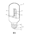
- FIG. 8 shows a cutaway sectional view of an incandescent bulb using the filament of the above embodiment.
- the incandescent lamp 1 includes a translucent airtight container 2, a filament 3 disposed inside the translucent airtight container 2, and a pair of lead wires that are electrically connected to both ends of the filament 3 and support the filament 3. 4 and 5.
- the translucent airtight container 2 is constituted by, for example, a glass bulb.
- the inside of the translucent airtight container 2 is in a high vacuum state of 10 ⁇ 1 to 10 ⁇ 6 Pa.
- a base 9 is joined to the sealing portion of the translucent airtight container 2.
- the base 9 includes a side electrode 6, a center electrode 7, and an insulating portion 8 that insulates the side electrode 6 from the center electrode 7.
- the end portion of the lead wire 4 is electrically connected to the side electrode 6, and the end portion of the lead wire 5 is electrically connected to the center electrode 7.
- the filament 3 is a filament according to any one of Embodiments 1 to 7, in which a wire-shaped base material is spirally wound and covered with a white scatterer layer to which impurity doping or metal particles are added. is there.
- the filament 3 has a very high reflectance from the ultraviolet light region to the infrared wavelength region and a low reflectance in the visible light region.
- high visible light luminous efficiency luminous efficiency
- emission of an infrared region can be suppressed and the visible light conversion efficiency of the visible light with respect to input electric power can be raised as a result. Thereby, an efficient energy saving type lighting bulb can be provided.
- the example in which the surface of the filament substrate is mirror-finished by mechanical polishing has been described.
- a substrate that is not mirror-polished can also be used.
- not only mechanical polishing but also mirror polishing using other methods is possible. For example, wet or dry etching, a method of contacting a smooth die during drawing, forging or rolling can be employed.
- the filament of the present invention is used as a filament of an incandescent bulb, but it can also be used other than an incandescent bulb.
- impurities for example, Er
- the filament can be efficiently heated to a high temperature with a small amount of input power due to the suppression effect of infrared light radiation (particularly suppression of long-wavelength infrared radiation), energy efficiency can be improved.
Landscapes
- Engineering & Computer Science (AREA)
- Manufacturing & Machinery (AREA)
- Non-Portable Lighting Devices Or Systems Thereof (AREA)
- Optical Elements Other Than Lenses (AREA)
Priority Applications (1)
| Application Number | Priority Date | Filing Date | Title |
|---|---|---|---|
| US14/368,795 US20140361675A1 (en) | 2011-12-26 | 2012-12-20 | Light source device and filament |
Applications Claiming Priority (2)
| Application Number | Priority Date | Filing Date | Title |
|---|---|---|---|
| JP2011284041A JP5964581B2 (ja) | 2011-12-26 | 2011-12-26 | 白熱電球 |
| JP2011-284041 | 2011-12-26 |
Publications (1)
| Publication Number | Publication Date |
|---|---|
| WO2013099760A1 true WO2013099760A1 (ja) | 2013-07-04 |
Family
ID=48697249
Family Applications (1)
| Application Number | Title | Priority Date | Filing Date |
|---|---|---|---|
| PCT/JP2012/083089 Ceased WO2013099760A1 (ja) | 2011-12-26 | 2012-12-20 | 光源装置、および、フィラメント |
Country Status (3)
| Country | Link |
|---|---|
| US (1) | US20140361675A1 (enExample) |
| JP (1) | JP5964581B2 (enExample) |
| WO (1) | WO2013099760A1 (enExample) |
Cited By (1)
| Publication number | Priority date | Publication date | Assignee | Title |
|---|---|---|---|---|
| JP2015103493A (ja) * | 2013-11-28 | 2015-06-04 | スタンレー電気株式会社 | 白熱電球およびフィラメント |
Families Citing this family (5)
| Publication number | Priority date | Publication date | Assignee | Title |
|---|---|---|---|---|
| JP5989984B2 (ja) * | 2011-10-27 | 2016-09-07 | スタンレー電気株式会社 | 白熱電球 |
| JP5975816B2 (ja) | 2012-09-21 | 2016-08-23 | スタンレー電気株式会社 | 白熱電球、その製造方法、および、フィラメント |
| JP6487621B2 (ja) * | 2014-01-22 | 2019-03-20 | スタンレー電気株式会社 | 赤外光源 |
| CN104808436B (zh) * | 2014-01-27 | 2017-11-24 | 太阳油墨(苏州)有限公司 | 碱显影型感光性树脂组合物、干膜和固化物、以及印刷电路板 |
| JP6371075B2 (ja) * | 2014-02-21 | 2018-08-08 | スタンレー電気株式会社 | フィラメント |
Citations (3)
| Publication number | Priority date | Publication date | Assignee | Title |
|---|---|---|---|---|
| JPH10289689A (ja) * | 1997-04-11 | 1998-10-27 | Sony Corp | ランプ電極の構造 |
| JP2006520074A (ja) * | 2003-03-06 | 2006-08-31 | チ・エレ・エッフェ・ソシエタ・コンソルティーレ・ペル・アチオニ | 白熱光源用の高性能エミッタ |
| JP2011124206A (ja) * | 2009-11-11 | 2011-06-23 | Stanley Electric Co Ltd | 可視光源 |
Family Cites Families (6)
| Publication number | Priority date | Publication date | Assignee | Title |
|---|---|---|---|---|
| US3973155A (en) * | 1975-01-31 | 1976-08-03 | Westinghouse Electric Corporation | Incandescent source of visible radiations |
| JPS56145652A (en) * | 1980-04-11 | 1981-11-12 | Rikuun Denki Kk | Bulb filament |
| JPS57174853A (en) * | 1981-04-21 | 1982-10-27 | Masamitsu Kawakami | Method of producing ceramic coating type bulb filament |
| JP2002222638A (ja) * | 2001-01-26 | 2002-08-09 | Oshino Denki Seisakusho:Kk | ガス等のセンサー・濃度検知器などに用いる赤外線放射光源 |
| US7851985B2 (en) * | 2006-03-31 | 2010-12-14 | General Electric Company | Article incorporating a high temperature ceramic composite for selective emission |
| JP5506514B2 (ja) * | 2010-04-07 | 2014-05-28 | スタンレー電気株式会社 | 赤外光源 |
-
2011
- 2011-12-26 JP JP2011284041A patent/JP5964581B2/ja not_active Expired - Fee Related
-
2012
- 2012-12-20 WO PCT/JP2012/083089 patent/WO2013099760A1/ja not_active Ceased
- 2012-12-20 US US14/368,795 patent/US20140361675A1/en not_active Abandoned
Patent Citations (3)
| Publication number | Priority date | Publication date | Assignee | Title |
|---|---|---|---|---|
| JPH10289689A (ja) * | 1997-04-11 | 1998-10-27 | Sony Corp | ランプ電極の構造 |
| JP2006520074A (ja) * | 2003-03-06 | 2006-08-31 | チ・エレ・エッフェ・ソシエタ・コンソルティーレ・ペル・アチオニ | 白熱光源用の高性能エミッタ |
| JP2011124206A (ja) * | 2009-11-11 | 2011-06-23 | Stanley Electric Co Ltd | 可視光源 |
Cited By (1)
| Publication number | Priority date | Publication date | Assignee | Title |
|---|---|---|---|---|
| JP2015103493A (ja) * | 2013-11-28 | 2015-06-04 | スタンレー電気株式会社 | 白熱電球およびフィラメント |
Also Published As
| Publication number | Publication date |
|---|---|
| JP5964581B2 (ja) | 2016-08-03 |
| US20140361675A1 (en) | 2014-12-11 |
| JP2013134873A (ja) | 2013-07-08 |
Similar Documents
| Publication | Publication Date | Title |
|---|---|---|
| JP5964581B2 (ja) | 白熱電球 | |
| US9214330B2 (en) | Light source device and filament | |
| JP6223186B2 (ja) | 光源装置、および、フィラメント | |
| US7487781B2 (en) | Energy converter and method of making the same | |
| HU199195B (en) | Electric lamp with improved current lead-in | |
| CN1333549A (zh) | 荧光灯和具有改进了发光效率的高强度放电灯 | |
| CN1842891A (zh) | 能量变换装置 | |
| CN1527355A (zh) | 带红外线反射涂层和带反射镜及红外线反射涂层的卤素灯 | |
| JP2003051284A (ja) | 蛍光ランプおよび照明器具 | |
| US9252006B2 (en) | Incandescent bulb, filament, and method for manufacturing filament | |
| JP6153734B2 (ja) | 光源装置 | |
| JP2016015260A (ja) | フィラメント、それを用いた光源、および、フィラメントの製造方法 | |
| JP2014112477A (ja) | 光源装置およびフィラメント | |
| JP6255189B2 (ja) | 発光体、光源装置、熱放射装置、熱電子放出装置および白熱電球 | |
| JP6239839B2 (ja) | 光源装置、および、フィラメント | |
| JP2010153221A (ja) | 高圧放電ランプおよび照明装置 | |
| Gendre | Incandescent lamps | |
| CN1894765A (zh) | 低压汞蒸气放电灯 | |
| JP2015185221A (ja) | フィラメントおよび光源装置 | |
| JP2014143129A (ja) | フィラメントの製造方法 | |
| JP2014164866A (ja) | フィラメント、および、その製造方法 | |
| JP6253313B2 (ja) | フィラメント、および、それを用いた光源 | |
| JP2015041580A (ja) | フィラメントおよび光源 | |
| CN1723533A (zh) | 金属卤灯 | |
| JP2015156314A (ja) | フィラメント、それを用いた光源およびヒーター |
Legal Events
| Date | Code | Title | Description |
|---|---|---|---|
| 121 | Ep: the epo has been informed by wipo that ep was designated in this application |
Ref document number: 12862398 Country of ref document: EP Kind code of ref document: A1 |
|
| WWE | Wipo information: entry into national phase |
Ref document number: 14368795 Country of ref document: US |
|
| NENP | Non-entry into the national phase |
Ref country code: DE |
|
| 122 | Ep: pct application non-entry in european phase |
Ref document number: 12862398 Country of ref document: EP Kind code of ref document: A1 |