WO2013084564A1 - 光分岐素子および光分岐回路 - Google Patents
光分岐素子および光分岐回路 Download PDFInfo
- Publication number
- WO2013084564A1 WO2013084564A1 PCT/JP2012/074501 JP2012074501W WO2013084564A1 WO 2013084564 A1 WO2013084564 A1 WO 2013084564A1 JP 2012074501 W JP2012074501 W JP 2012074501W WO 2013084564 A1 WO2013084564 A1 WO 2013084564A1
- Authority
- WO
- WIPO (PCT)
- Prior art keywords
- waveguide
- waveguides
- strip
- optical branching
- shaped
- Prior art date
- Legal status (The legal status is an assumption and is not a legal conclusion. Google has not performed a legal analysis and makes no representation as to the accuracy of the status listed.)
- Ceased
Links
Images





Classifications
-
- G—PHYSICS
- G02—OPTICS
- G02B—OPTICAL ELEMENTS, SYSTEMS OR APPARATUS
- G02B6/00—Light guides; Structural details of arrangements comprising light guides and other optical elements, e.g. couplings
- G02B6/24—Coupling light guides
- G02B6/26—Optical coupling means
- G02B6/30—Optical coupling means for use between fibre and thin-film device
- G02B6/305—Optical coupling means for use between fibre and thin-film device and having an integrated mode-size expanding section, e.g. tapered waveguide
-
- G—PHYSICS
- G02—OPTICS
- G02B—OPTICAL ELEMENTS, SYSTEMS OR APPARATUS
- G02B6/00—Light guides; Structural details of arrangements comprising light guides and other optical elements, e.g. couplings
- G02B6/10—Light guides; Structural details of arrangements comprising light guides and other optical elements, e.g. couplings of the optical waveguide type
- G02B6/12—Light guides; Structural details of arrangements comprising light guides and other optical elements, e.g. couplings of the optical waveguide type of the integrated circuit kind
- G02B6/122—Basic optical elements, e.g. light-guiding paths
- G02B6/125—Bends, branchings or intersections
-
- G—PHYSICS
- G02—OPTICS
- G02B—OPTICAL ELEMENTS, SYSTEMS OR APPARATUS
- G02B6/00—Light guides; Structural details of arrangements comprising light guides and other optical elements, e.g. couplings
- G02B6/10—Light guides; Structural details of arrangements comprising light guides and other optical elements, e.g. couplings of the optical waveguide type
- G02B6/12—Light guides; Structural details of arrangements comprising light guides and other optical elements, e.g. couplings of the optical waveguide type of the integrated circuit kind
- G02B2006/12133—Functions
- G02B2006/1215—Splitter
Definitions
- the present invention relates to an optical branching device and an optical branching circuit using an optical waveguide.
- a technique for reducing the loss of the optical branching device by providing a strip-shaped waveguide with respect to the branching waveguide is disclosed.
- a band-shaped waveguide is provided in a portion from a slab waveguide to an arrayed waveguide of an arrayed-waveguide grating (AWG) to reduce the loss.
- AWG arrayed-waveguide grating
- a band-like waveguide is provided in a portion from a tapered waveguide to a branching waveguide of a Y-branch type optical branching element to reduce loss.
- the present invention has been made in view of the above, and an object of the present invention is to provide an optical branching device and an optical branching circuit that can realize even lower loss.
- an optical branching device includes an input waveguide, a tapered waveguide connected to the input waveguide, the tapered waveguide connected to the input waveguide, and the input
- the two branch waveguides arranged so as to form a Y shape together with the waveguide and the taper waveguide are connected between the two branch waveguides and outside the two branch waveguides.
- a plurality of strip-shaped waveguides provided so as not to protrude and having a width that decreases as the distance from the tapered waveguide increases.
- the optical branching element according to the present invention is characterized in that, in the above invention, the plurality of strip-shaped waveguides are provided separated by a predetermined interval.
- optical branching element according to the present invention is characterized in that, in the above-mentioned invention, 10 or less of the strip waveguides are provided.
- the optical branching element according to the present invention is provided so as to fill a space between the plurality of strip-shaped waveguides, and the buffer is formed so that the height decreases as the distance from the tapered waveguide increases. It further has a waveguide.
- the optical branching element according to the present invention is characterized in that, in the above invention, the taper waveguide and the strip waveguide are separated by a predetermined gap.
- the optical branching element according to the present invention is the optical branching element according to the above-described invention, wherein the two branching waveguides and the plurality of strip-shaped waveguides are configured by curved waveguides, and each of the branching waveguides and each of the strip-shaped waveguides.
- the waveguide is orthogonal to the waveguide.
- the two branching waveguides and the plurality of strip-shaped waveguides are configured by straight waveguides in the above invention, and the light propagation direction in the input waveguides And the respective strip-shaped waveguides are orthogonal to each other.
- the optical branching element according to the present invention is characterized in that it is formed on a quartz substrate in the above invention.
- an optical branching circuit according to the present invention is characterized in that the optical branching element described in the above invention is configured in a multistage connection.
- FIG. 1 is a schematic plan view of the optical branching device according to the first embodiment.
- 2 is a cross-sectional view of the optical branching element shown in FIG. 1 taken along line XX.
- 3 is a cross-sectional view of the optical branching element shown in FIG. 1 taken along line YY.
- FIG. 4 is a schematic cross-sectional view of an optical branching element according to Modification 1 of Embodiment 1.
- FIG. 5 is a schematic cross-sectional view of an optical branching element according to Modification 2 of Embodiment 1.
- FIG. 6 is a schematic plan view of the optical branching device according to the second embodiment.
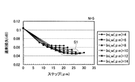
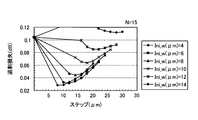
- FIG. 7 is a diagram illustrating the relationship between the step of the band-shaped waveguide and the excess loss of the optical branching element when the first width of the band-shaped waveguide is changed when the number of the band-shaped waveguides is five.
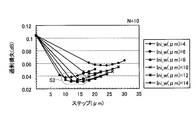
- FIG. 8 is a diagram showing the relationship between the step of the band-shaped waveguide and the excess loss of the optical branching element when the first width of the band-shaped waveguide is changed when the number of the band-shaped waveguides is 10.
- FIG. 9 is a diagram illustrating the relationship between the step of the strip waveguide and the excess loss of the optical branching element when the first width of the strip waveguide is changed when the number of strip waveguides is 15.
- FIG. 10 is a diagram illustrating the relationship between the step of the strip waveguide and the excess loss of the optical branching element when the first width of the strip waveguide is changed when the number of strip waveguides is 20.
- FIG. FIG. 11 is a schematic plan view of the optical branching circuit according to the third embodiment.
- FIG. 12 is a schematic plan view of the optical branching circuit according to the fourth embodiment.
- FIG. 13 is a schematic plan view of a conventional optical branching element.
- FIG. 1 is a schematic plan view of an optical branching element according to Embodiment 1 of the present invention.
- 2 is a cross-sectional view of the optical branching element 10 shown in FIG. 3 is a cross-sectional view of the optical branching element 10 shown in FIG. 1 taken along the line YY.
- the optical branching element 10 includes an input waveguide 1, a tapered waveguide 2 connected to the input waveguide, two branching waveguides 3a and 3b, and five strip-shaped waveguides 4a to 4b. 4e and buffer waveguide 5 are provided.
- the input waveguide 1 is formed in a substantially linear shape, and light having a wavelength of, for example, a 1.31 ⁇ m band or a 1.55 ⁇ m band is input from the left side of the paper.
- the tapered waveguide 2 is connected to the light output side of the input waveguide 1 and is formed so that the width increases along the propagation direction of the light input to the input waveguide 1.
- the two branching waveguides 3a and 3b are connected to the light output side of the tapered waveguide 2 and are constituted by curved waveguides.
- the branching waveguides 3 a and 3 b are arranged so as to form a Y shape together with the input waveguide 1 and the tapered waveguide 2.
- the light branching element 10 is configured as a Y branching element.
- the branching waveguides 3 a and 3 b are formed on the quartz substrate 11, and are formed so as to be surrounded by the upper clad layer 12 at the top and sides.
- the input waveguide 1 and the tapered waveguide 2 are also formed on the quartz substrate 11 and are formed so that the upper clad layer 12 surrounds the upper and side portions.
- the quartz substrate 11 and the upper cladding layer 12 are made of quartz glass such as pure quartz glass.
- the input waveguide 1, the tapered waveguide 2, and the branching waveguides 3 a and 3 b are made of titanium (Ti) or germanium (Ge) so that the relative refractive index difference with respect to the quartz substrate 11 and the upper cladding layer 12 is 0.4%.
- the cross-sectional size of the input waveguide 1 and the branching waveguides 3a and 3b is 7 ⁇ m ⁇ 7 ⁇ m.
- the input waveguide 1 and the branching waveguides 3a and 3b can propagate the input light having a wavelength of 1.31 ⁇ m band or 1.55 ⁇ m band in a single mode.
- the curvature radius R of the branching waveguides 3a and 3b with respect to the center O of the arc formed by the branching waveguides 3a and 3b is set to a curvature radius that does not cause a problem of bending loss with respect to input light.
- the radius of curvature can be set to 15000 ⁇ m.
- the size of the tapered waveguide 2 is, for example, 7 ⁇ m as in the case of the input waveguide 1, and the width is formed so as to increase from 7 ⁇ m to 14 ⁇ m, for example.
- the strip-shaped waveguides 4a to 4e are formed of curved waveguides, connect the branch waveguides 3a and 3b, and do not protrude outside the branch waveguides 3a and 3b. It is provided as follows.
- the buffer waveguide 5 is provided so as to fill the space between the strip-shaped waveguides 4a to 4d, and is formed so that the height decreases as the distance from the taper waveguide 2 increases.
- the strip-shaped waveguides 4 a to 4 e and the buffer waveguide 5 are also formed on the quartz substrate 11 and are formed so as to be surrounded by the upper clad layer 12 at the upper and side portions.
- the strip-shaped waveguides 4a to 4e and the buffer waveguide 5 are increased in refractive index by adding Ti, Ge, or the like so that the relative refractive index difference with respect to the quartz substrate 11 and the upper cladding layer 12 is 0.4%.
- the strip waveguides 4a to 4e will be further described.
- the gap G is separated between the tapered waveguide 2 and the strip-shaped waveguide 4 a closest to the tapered waveguide 2.
- the gap G is, for example, 1.5 ⁇ m.
- the width of the strip-shaped waveguide 4a closest to the tapered waveguide 2 is defined as a first width W.
- Each of the strip-shaped waveguides 4a to 4e is provided so as to be separated by a predetermined interval (step S) of, for example, 22 ⁇ m, and is formed so that the width decreases as the distance from the tapered waveguide 2 increases. .
- the widths of the strip-shaped waveguides 4b, 4c, 4d, and 4e are about 10.6 ⁇ m, 7.2 ⁇ m, 3.8 ⁇ m, and 0.5 ⁇ m, The width is formed to decrease substantially linearly.
- the height of the buffer waveguide 5 between the tapered waveguide 2 and the strip-shaped waveguide 4a is 3.5 ⁇ m, the depth of the gap between the tapered waveguide 2 and the strip-shaped waveguide 4a is 3. It is 5 ⁇ m.
- the gap depths are 4.8 ⁇ m, 6.0 ⁇ m, and 6.5 ⁇ m between the strip-shaped waveguides 4 a and 4 b, between the strip-shaped waveguides 4 b and 4 c, and between the strip-shaped waveguides 4 c and 4 d, respectively.
- each of the branched waveguides 3a and 3b and each of the strip-shaped waveguides 4a to 4e are orthogonal to each other.
- the fact that the branching waveguide 3b and the strip-shaped waveguide 4e are orthogonal to each other means that the arc tangent direction d1 formed by the branching waveguide 3b and the arc-tangent direction d2 formed by the strip-shaped waveguide 4e are: Means that they are orthogonal to each other.
- this optical branching element 10 can be manufactured using, for example, the following quartz PLC (Planar Lightwave Circuit) manufacturing process.
- a quartz glass layer to which Ti or Ge for forming each optical waveguide is added is deposited on a quartz substrate 11 by a flame deposition (FHD) method, and this is made into a transparent glass.
- FHD flame deposition
- the quartz glass layer is formed into the pattern of each optical waveguide by photolithography using reactive ion etching and reactive ion etching.
- the buffer waveguides 5 having different heights can be formed by adjusting reactive ion etching or photolithography conditions.
- quartz glass for forming the upper clad layer 12 is again deposited by the FHD method, and this is made into transparent glass to form the upper clad layer 12. Thereby, the optical branching element 10 can be manufactured.
- the input waveguide 1 When light is input from the input waveguide 1 of the optical branching element 10, the input waveguide 1 guides the light in a single mode and inputs it to the tapered waveguide 2.
- the tapered waveguide 2 performs mode conversion so that the input light is input to the branching waveguides 3a and 3b in a single mode.
- the branching waveguides 3a and 3b guide the mode-converted light in a single mode, respectively.
- the strip-shaped waveguides 4a to 4e suppress the leakage of radiation mode light as a part of the light cannot be sufficiently coupled between the tapered waveguide 2 and the branching waveguides 3a and 3b, thereby improving the coupling efficiency.
- the optical loss of the optical branching element 10 is reduced.
- each of the strip-shaped waveguides 4a to 4e is formed so that the width decreases as the distance from the tapered waveguide 2 increases, mode conversion from the tapered waveguide 2 to the branching waveguides 3a and 3b can be performed smoothly. In addition, the optical loss is further reduced.
- the buffer waveguide 5 is formed so that the height decreases as the distance from the taper waveguide 2 increases, the strip-shaped waveguides 4a to 4e are not completely discretized. Therefore, the mode conversion is performed more smoothly, so that the optical loss is further reduced.
- each of the branching waveguides 3a and 3b and each of the strip-like waveguides 4a to 4e are orthogonal to each other, it is possible to suppress light loss due to crosstalk at the coupling portion.
- branch waveguides 3a and 3b are formed in the vicinity of the taper waveguide 2 in the process for forming the upper cladding layer 12. Can fall into each other. As a result, the distance between the branched optical waveguides 3a and 3b can be narrowed, so that the light output from the tapered waveguide 2 can be more efficiently coupled to the branched waveguides 3a and 3b.
- the strip-like waveguides 4a to 4e are provided so as not to protrude outside the branching waveguides 3a and 3b. This further reduces optical loss.
- FIG. 13 is a schematic plan view of a conventional optical branching element.
- An optical branching device 40 shown in FIG. 13 includes an input waveguide 41, a tapered waveguide 42 connected to the input waveguide 41, two branching waveguides 43a and 43b, and thirty strip-shaped waveguides 44a to 44 ⁇ . It has.
- the optical branching element 40 is greatly different from the optical branching element 10 in that the strip-like waveguides 44a to 44 ⁇ protrude outside the branching waveguides 43a and 43b.
- the clad layer 12 may be largely deformed by being collapsed. Due to this deformation, the side portions of the respective branching waveguides 43a and 43b are also deformed, so that there is a case where the loss reduction as designed in the waveguide pattern cannot be realized.
- the tapered waveguide guides light confined in the width direction, so that the power distribution of light has a distribution shape with high power even at the side. Therefore, when the side portion of the branching waveguide near the tapered waveguide is deformed by the protruding portion, the influence on the optical loss is increased.
- the strip-like waveguides 4a to 4e are provided so as not to protrude outside the branching waveguides 3a and 3b.
- the deformations as described above do not occur, so that further reduction of optical loss closer to the design value is realized.
- the optical branching element 10 has a further reduced optical loss.
- FIG. 4 is a schematic cross-sectional view of an optical branching element according to Modification 1 of Embodiment 1.
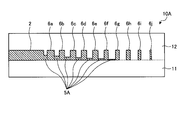
- An optical branching element 10A shown in FIG. 4 is different from the optical branching element 10 shown in FIG. 1 in that it replaces the five strip-shaped waveguides 4a to 4e and the buffer waveguide 5 with ten strip-shaped waveguides 6a to 6j. And a waveguide 5A.
- the strip-shaped waveguides 6a to 6j are provided so as to connect the branch waveguides 3a and 3b and not to protrude outside the branch waveguides 3a and 3b.
- the buffering waveguide 5A is provided so as to fill the space between the strip-shaped waveguides 6a to 6g, and is formed so that the height decreases as the distance from the tapered waveguide 2 increases.
- the taper waveguide 2 and the strip-shaped waveguide 6a closest to the taper waveguide 2 are separated by a gap of 1.5 ⁇ m, for example.
- Each of the strip-shaped waveguides 6a to 6j is provided so as to be separated by a step of 22 ⁇ m, for example, and is formed so that the width decreases as the distance from the tapered waveguide 2 increases.
- the width of each strip-shaped waveguide 6b, 6c, 6d, 6e, 6f, 6g, 6h, 6i, 6j is about 12.5 ⁇ m, 11.0 ⁇ m, 9 0.5 ⁇ m, 8.0 ⁇ m, 6.5 ⁇ m, 5.0 ⁇ m, 3.5 ⁇ m, 2.0 ⁇ m, and 0.5 ⁇ m, and the width is formed to decrease substantially linearly.
- the height of the strip-shaped waveguides 6a to 6j is 7 ⁇ m, and the height of the buffer waveguide 5A between the tapered waveguide 2 and the strip-shaped waveguide 6a is 3.5 ⁇ m.
- the depth of the gap between the waveguide 6a is 3.5 ⁇ m.
- the depth of the gap is as follows: between the strip waveguides 6a and 6b, between the strip waveguides 6b and 6c, between the strip waveguides 6c and 6d, between the strip waveguides 6d and 6e, between the strip waveguides 6e and 6f, and between the strip waveguides.
- the distances between the waveguides 6f and 6g are 4.2 ⁇ m, 5.0 ⁇ m, 5.7 ⁇ m, 6.5 ⁇ m, 6.8 ⁇ m, and 6.9 ⁇ m, respectively.
- the optical branching element 10A according to the first modification since the strip-shaped waveguides 6a to 6j do not protrude outside the branching waveguides 3a and 3b, the optical loss is further reduced.
- FIG. 5 is a schematic cross-sectional view of an optical branching element according to Modification 2 of Embodiment 1.
- An optical branching element 10B shown in FIG. 5 has a configuration in which the buffer waveguide 5 is omitted from the optical branching element 10 shown in FIG.
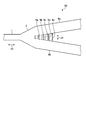
- FIG. 6 is a schematic plan view of the optical branching device according to the second embodiment.
- the optical branching device 20 is different from the optical branching device 10 shown in FIG. 1 in that two branching waveguides 3a and 3b and five strip-like waveguides 4a to 4e are replaced with two.
- Branching waveguides 8a and 8b and five strip-shaped waveguides 9a to 9e are provided.
- the two branching waveguides 8a and 8b are connected to the light output side of the tapered waveguide 2 and are constituted by straight waveguides.
- the branching waveguides 8 a and 8 b are arranged so as to form a Y shape together with the input waveguide 1 and the tapered waveguide 2.
- the light branching element 20 is configured as a Y branching element.
- the branched waveguides 8a and 8b are also formed on the quartz substrate and are formed so that the upper and side portions are surrounded by the upper cladding layer.
- the branching waveguides 8a and 8b are made of silica-based glass whose refractive index is increased so that the relative refractive index difference with respect to the quartz substrate and the upper cladding layer is 0.4%.
- the cross-sectional size of the branching waveguides 8a and 8b is 7 ⁇ m ⁇ 7 ⁇ m.
- the strip-shaped waveguides 9a to 9e are constituted by straight waveguides, and are provided so as to connect between the branched waveguides 8a and 8b and not to protrude outside the branched waveguides 8a and 8b.
- the strip-like waveguides 9a to 9e are also formed on the quartz substrate and are formed so that the upper and side portions are surrounded by the upper cladding layer, and the relative refractive index difference with respect to the quartz substrate and the upper cladding layer is 0.4%. It is made of quartz glass with an increased refractive index so that
- the gap between the tapered waveguide 2 and the strip-shaped waveguide 9a closest to the tapered waveguide 2 the steps between the strip-shaped waveguides 9a to 9e, and the widths of the strip-shaped waveguides 9a to 9e are: It is set similarly to the strip-shaped waveguides 4a to 4e.
- the light propagation direction d3 in the input waveguide 1 and the longitudinal direction d4 of each of the strip-shaped waveguides 9a to 9e are orthogonal to each other. As a result, the loss due to the intersection can be minimized, and the effect of increasing the coupling efficiency is maximized.
- FIGS. 7 to 10 show the steps of the band-shaped waveguide and the excess of the optical branching element when the first width of the band-shaped waveguide is changed when the number of the band-shaped waveguides is 5, 10, 15, 20 respectively. It is a figure which shows the relationship with a loss.
- the shape of the optical branching element in FIGS. 7 to 10 is based on the shape of the optical branching element 10 according to the first embodiment, and the number of strip-shaped waveguides is changed to 10, 15, and 20.
- the width of the strip-shaped waveguide farthest from the tapered waveguide is fixed to 0.5 ⁇ m, and the width of each strip-shaped waveguide is increased as the distance from the tapered waveguide increases.
- the width of the waveguide was set so as to decrease substantially linearly.
- N indicates the number of strip-shaped waveguides
- Ini_w in the legend indicates the first width of the strip-shaped waveguides.
- the number of strip-shaped waveguides is preferably 10 or less. Further, the lower limit of the number of the strip-shaped waveguides is more preferably 2 or more, and if it is 5 or more, the effect of increasing the coupling efficiency is increased.
- FIG. 11 is a schematic plan view of the optical branching circuit according to the third embodiment.
- this optical branching circuit 100 seven optical branching elements 10 according to Embodiment 1 are connected in multiple stages in a tree shape to form a 1 ⁇ 8 optical branching circuit.
- the output waveguides 30 are connected to the output sides of the four optical branching elements 10 on the 8-port side.
- the optical branch circuit 100 includes the optical branch element 10 according to the first embodiment, the optical branch circuit 100 is an optical branch circuit in which the optical loss is further reduced.
- FIG. 12 is a schematic plan view of the optical branching circuit according to the fourth embodiment.
- 31 optical branching elements 10 according to the first embodiment are connected in multiple stages in a tree shape to form a 1 ⁇ 32 optical branching circuit.
- the output waveguides 30 are connected to the output sides of the 16 optical branching elements 10 on the 32 port side.
- this optical branch circuit 200 also includes the optical branch element 10 according to Embodiment 1, it is an optical branch circuit in which the optical loss is further reduced.
- Example 1 a 1 ⁇ 8 optical branch circuit having the configuration shown in FIG. 11 using the optical branch device having the configuration shown in FIG. 1 was manufactured using the above-described PLC manufacturing process.
- the first width of the strip waveguide is 14 ⁇ m
- the steps are 22 ⁇ m
- the number is 5
- the gap between the taper waveguide and the strip waveguide is 1.5 ⁇ m.
- the characteristics of each waveguide are the values exemplified in the first embodiment. That is, for example, the branch waveguide has a cross-sectional size of 7 ⁇ m ⁇ 7 ⁇ m, and a relative refractive index difference with respect to the quartz substrate and the upper cladding layer is 0.4%.
- Comparative Example 1 a 1 ⁇ 8 optical branch circuit having the configuration shown in FIG. 11 using the optical branch element having the configuration shown in FIG. 13 was produced.
- the first width of the strip waveguide was 8 ⁇ m
- the steps were 20 ⁇ m
- the number was 30, and the gap between the taper waveguide and the strip waveguide was 1.5 ⁇ m.
- the width of the band-shaped waveguide farthest from the taper waveguide is set to 0.5 ⁇ m
- the width of each band-shaped waveguide is set so that the width of the band-shaped waveguide decreases approximately linearly as the distance from the taper waveguide increases.
- the length of the strip-like waveguide protruding outside each branching waveguide was set to about 100 ⁇ m.
- the average loss of the insertion loss of the eight ports of the manufactured optical branch circuit of Example 1 and Comparative Example 1 was measured at a wavelength of 1.31 ⁇ m or 1.55 ⁇ m. Then, in Comparative Example 1, the average loss was 9.85 dB (@ 1.31 ⁇ m) and 9.81 dB (@ 1.55 ⁇ m). On the other hand, in Example 1, the average loss was 9.64 dB (@ 1.31 ⁇ m) and 9.63 dB (@ 1.55 ⁇ m), which was a low loss compared to Comparative Example 1.
- Example 2 As Example 2 of the present invention, a 1 ⁇ 8 optical branch circuit having the configuration shown in FIG. 11 using the optical branch element having the configuration shown in FIG. 4 was produced.
- the first width of the strip-shaped waveguide was 8 ⁇ m
- the steps were 14 ⁇ m
- the number was 10
- the gap between the tapered waveguide and the strip-shaped waveguide was 1.5 ⁇ m.
- the characteristics of each waveguide are the values exemplified in the first modification.
- the average loss of the insertion loss of the eight ports of the manufactured optical branch circuit of Example 2 was measured at a wavelength of 1.31 ⁇ m or 1.55 ⁇ m. Then, the average loss was 9.73 dB (@ 1.31 ⁇ m) and 9.68 dB (@ 1.55 ⁇ m), which is a low loss compared to Comparative Example 1.
- Example 3 Comparative Example 2
- a 1 ⁇ 32 optical branch circuit having the configuration shown in FIG. 12 using the same optical branching element as in Example 1 was manufactured using the above-described PLC manufacturing process.
- Comparative Example 2 a 1 ⁇ 32 optical branching circuit having the configuration shown in FIG. 12 using the same optical branching element as Comparative Example 1 was produced.
- the average loss of the insertion loss of 32 ports of the manufactured optical branch circuit of Example 3 and Comparative Example 2 was measured at a wavelength of 1.31 ⁇ m or 1.55 ⁇ m. Then, in Comparative Example 2, the average loss was 16.46 dB (@ 1.31 ⁇ m) and 16.39 dB (@ 1.55 ⁇ m). On the other hand, in Example 3, the average loss was 16.06 dB (@ 1.31 ⁇ m) and 16.02 dB (@ 1.55 ⁇ m), which is a low loss compared to Comparative Example 2.
- Example 4 As Example 4 of the present invention, a 1 ⁇ 8 optical branching circuit having the configuration shown in FIG. 11 using an optical branching device having the configuration shown in FIG.
- the first width of the strip waveguide is 14 ⁇ m
- the steps are 22 ⁇ m
- the number is 5
- the gap between the taper waveguide and the strip waveguide is 1.5 ⁇ m.
- the characteristics of each waveguide are the values exemplified in the second embodiment.
- the average loss of the insertion loss of the eight ports of the manufactured optical branch circuit of Example 4 was measured at a wavelength of 1.31 ⁇ m or 1.55 ⁇ m. Then, the average loss was 9.66 dB (@ 1.31 ⁇ m) and 9.65 dB (@ 1.55 ⁇ m), which is a low loss compared to Comparative Example 1.
- Example 5 As Example 5 of the present invention, a 1 ⁇ 8 optical branch circuit having the configuration shown in FIG. 11 using the optical branch element having the configuration shown in FIG. 5 was produced.
- the first width of the strip-shaped waveguide was 14 ⁇ m
- the steps were 24 ⁇ m
- the number was 5
- the gap between the tapered waveguide and the strip-shaped waveguide was 1.5 ⁇ m.
- the characteristics of each waveguide are the values exemplified in the second modification.
- the average loss of the insertion loss of the eight ports of the manufactured optical branch circuit of Example 5 was measured at a wavelength of 1.31 ⁇ m or 1.55 ⁇ m. Then, the average loss was 9.70 dB (@ 1.31 ⁇ m) and 9.65 dB (@ 1.55 ⁇ m), which was a low loss compared to Comparative Example 1.
- the optical branching element and the optical branching circuit are made of quartz glass, but other glass materials and organic materials can be used as appropriate.
- the manufacturing method is not limited to the PLC process, and various manufacturing methods capable of manufacturing an optical branching device and an optical branching circuit made of a waveguide can be used.
- the numerical values of the characteristics such as the cross-sectional size, width, and relative refractive index difference of each waveguide described in the above embodiments and examples are examples, and constituent materials of the optical branching element and the optical branching circuit, It can be appropriately set according to desired characteristics.
- the present invention is not limited by the above embodiment. What was comprised combining each component mentioned above suitably is also contained in this invention.
- a buffer waveguide may be provided as in the first embodiment. Further effects and modifications can be easily derived by those skilled in the art. Therefore, the broader aspect of the present invention is not limited to the above-described embodiment, and various modifications can be made.
- optical branching element and the optical branching circuit according to the present invention are suitable for use in the field of optical communication.
Landscapes
- Physics & Mathematics (AREA)
- General Physics & Mathematics (AREA)
- Optics & Photonics (AREA)
- Engineering & Computer Science (AREA)
- Microelectronics & Electronic Packaging (AREA)
- Optical Integrated Circuits (AREA)
Abstract
入力導波路と、前記入力導波路に接続したテーパ導波路と、前記テーパ導波路に接続し、前記入力導波路およびテーパ導波路とともにY字形状を構成するように配置された2本の分岐導波路と、前記2本の分岐導波路の間を接続し、かつ前記2本の分岐導波路の外側に突出しないように設けられ、前記テーパ導波路から離間するにつれて幅が減少するように形成された複数の帯状導波路と、を備える。これによって、より一層の低損失を実現できる光分岐素子および光分岐回路を提供することができる。
Description
本発明は、光導波路を用いた光分岐素子および光分岐回路に関する。
従来の光導波路を用いた光分岐素子において、分岐導波路に対して帯状導波路を設けることによって、光分岐素子を低損失化する技術が開示されている。たとえば、特許文献1~3では、アレイ導波路回折格子(Arrayed-Waveguide Grating:AWG)のスラブ導波路からアレイ導波路までの部分に帯状導波路を設け、低損失化を行っている。また、特許文献4では、Y分岐型の光分岐素子のテーパ導波路から分岐導波路までの部分に帯状導波路を設け、低損失化を行っている。
しかしながら、本願発明者らが、帯状導波路を備えるY分岐型の光分岐素子を作製し、その特性を精査したところ、設計上予測された所望の低損失化が実現できていない場合があるという問題があった。
本発明は、上記に鑑みてなされたものであって、より一層の低損失を実現できる光分岐素子および光分岐回路を提供することを目的とする。
上述した課題を解決し、目的を達成するために、本発明に係る光分岐素子は、入力導波路と、前記入力導波路に接続したテーパ導波路と、前記テーパ導波路に接続し、前記入力導波路およびテーパ導波路とともにY字形状を構成するように配置された2本の分岐導波路と、前記2本の分岐導波路の間を接続し、かつ前記2本の分岐導波路の外側に突出しないように設けられ、前記テーパ導波路から離間するにつれて幅が減少するように形成された複数の帯状導波路と、を備えることを特徴とする。
また、本発明に係る光分岐素子は、上記の発明において、前記複数の帯状導波路は所定の間隔だけ離間して設けられていることを特徴とする。
また、本発明に係る光分岐素子は、上記の発明において、10本以下の前記帯状導波路を備えることを特徴とする。
また、本発明に係る光分岐素子は、上記の発明において、前記複数の帯状導波路の間を埋めるように設けられ、前記テーパ導波路から離間するにつれて高さが減少するように形成された緩衝導波路をさらに備えることを特徴とする。
また、本発明に係る光分岐素子は、上記の発明において、前記テーパ導波路と前記帯状導波路との間は所定のギャップだけ離間していることを特徴とする。
また、本発明に係る光分岐素子は、上記の発明において、前記2本の分岐導波路および前記複数の帯状導波路は曲線導波路で構成されており、かつ前記各分岐導波路と前記各帯状導波路とが直交していることを特徴とする。
また、本発明に係る光分岐素子は、上記の発明において、前記2本の分岐導波路および前記複数の帯状導波路は直線導波路で構成されており、かつ前記入力導波路における光の伝搬方向と前記各帯状導波路とが直交していることを特徴とする。
また、本発明に係る光分岐素子は、上記の発明において、石英基板上に形成されていることを特徴とする。
また、本発明に係る光分岐回路は、上記の発明に記載の光分岐素子が多段接続して構成されていることを特徴とする。
本発明によれば、より一層低損失の光分岐素子および光分岐回路を実現できるという効果を奏する。
以下に、図面を参照して本発明に係る光分岐素子および光分岐回路の実施の形態を詳細に説明する。なお、この実施の形態によりこの発明が限定されるものではない。また、各図面において、同一または対応する要素には適宜同一の符号を付している。さらに、図面は模式的なものであり、各層の厚みと幅との関係、各層の比率などは、現実のものとは異なる場合があることに留意する必要がある。図面の相互間においても、互いの寸法の関係や比率が異なる部分が含まれている場合がある。
(実施の形態1)
図1は、本発明の実施の形態1に係る光分岐素子の模式的な平面図である。図2は、図1に示す光分岐素子10のX-X線断面図である。図3は、図1に示す光分岐素子10のY-Y線断面図である。図1に示すように、光分岐素子10は、入力導波路1と、入力導波路に接続したテーパ導波路2と、2本の分岐導波路3a、3bと、5本の帯状導波路4a~4eと、緩衝導波路5とを備えている。
図1は、本発明の実施の形態1に係る光分岐素子の模式的な平面図である。図2は、図1に示す光分岐素子10のX-X線断面図である。図3は、図1に示す光分岐素子10のY-Y線断面図である。図1に示すように、光分岐素子10は、入力導波路1と、入力導波路に接続したテーパ導波路2と、2本の分岐導波路3a、3bと、5本の帯状導波路4a~4eと、緩衝導波路5とを備えている。
入力導波路1は、略直線状に形成されており、紙面左側から、たとえば1.31μm帯や1.55μm帯の波長の光が入力される。テーパ導波路2は、入力導波路1の光出力側に接続されており、入力導波路1に入力された光の伝搬方向に沿って幅が広がるように形成されている。2本の分岐導波路3a、3bは、テーパ導波路2の光出力側に接続されており、曲線導波路で構成されている。分岐導波路3a、3bは、入力導波路1およびテーパ導波路2とともに、Y字形状を構成するように配置されている。これによって、光分岐素子10は、Y分岐素子として構成されている。
図2に示すように、分岐導波路3a、3bは、石英基板11上に形成され、かつ上部クラッド層12に上部および側部を囲まれるように形成されている。なお、入力導波路1およびテーパ導波路2も、石英基板11上に形成され、かつ上部クラッド層12に上部および側部を囲まれるように形成されている。石英基板11および上部クラッド層12は、純石英ガラス等の石英系ガラスからなる。入力導波路1、テーパ導波路2、および分岐導波路3a、3bは、石英基板11および上部クラッド層12に対する比屈折率差が0.4%になるようにチタン(Ti)やゲルマニウム(Ge)等を添加して屈折率を高めた石英系ガラスからなる。入力導波路1および分岐導波路3a、3bの断面のサイズは7μm×7μmである。これによって、入力導波路1および分岐導波路3a、3bは、入力される波長1.31μm帯または1.55μm帯の光をシングルモードで伝搬することができる。また、分岐導波路3a、3bが形成する円弧の中心Oに対する分岐導波路3a、3bの曲率半径Rは、入力される光に対する曲げ損失が問題とならない程度の曲率半径とされる。たとえば、分岐導波路3a、3bの比屈折率差および断面のサイズが上記の値である場合は、曲率半径は15000μmとすることができる。
また、テーパ導波路2のサイズは、厚さは入力導波路1と同様にたとえば7μmであり、幅はたとえば7μmから14μmまで幅が広がるように形成されている。
つぎに、帯状導波路4a~4eおよび緩衝導波路5について説明する。図1、3に示すように、帯状導波路4a~4eは、曲線導波路で構成されており、分岐導波路3a、3bの間を接続し、かつ分岐導波路3a、3bの外側に突出しないように設けられている。
緩衝導波路5は、帯状導波路4a~4dの間を埋めるように設けられ、テーパ導波路2から離間するにつれて高さが減少するように形成されている。帯状導波路4a~4eおよび緩衝導波路5も、石英基板11上に形成され、かつ上部クラッド層12に上部および側部を囲まれるように形成されている。また、帯状導波路4a~4eおよび緩衝導波路5は、石英基板11および上部クラッド層12に対する比屈折率差が0.4%になるようにTiやGe等を添加して屈折率を高めた石英系ガラスからなる。
帯状導波路4a~4eについてさらに説明する。テーパ導波路2と、テーパ導波路2に最も近い帯状導波路4aとの間はギャップGだけ離間している。ギャップGはたとえば1.5μmである。以下、テーパ導波路2に最も近い帯状導波路4aの幅を第1幅Wとする。また、各帯状導波路4a~4eは、たとえば22μmである所定の間隔(ステップS)だけ離間して設けられており、かつテーパ導波路2から離間するにつれて幅が減少するように形成されている。たとえば、帯状導波路4aの第1幅Wを14μmとすると、各帯状導波路4b、4c、4d、4eの幅は、約10.6μm、7.2μm、3.8μm、0.5μmであり、幅が略線形に減少するように形成されている。また、テーパ導波路2と帯状導波路4aとの間における緩衝導波路5の高さは3.5μmであるため、テーパ導波路2と帯状導波路4aとの間のギャップの深さは3.5μmとなっている。また、ギャップの深さは、帯状導波路4a、4b間、帯状導波路4b、4c間、帯状導波路4c、4d間で、それぞれ4.8μm、6.0μm、6.5μmとなっている。
また、各分岐導波路3a、3bと、各帯状導波路4a~4eとは直交している。ここで、たとえば分岐導波路3bと帯状導波路4eが直交しているとは、分岐導波路3bが形成する円弧の接線の方向d1と、帯状導波路4eが形成する円弧の接線の方向d2とが、互いの接続部において直交することを意味する。
なお、この光分岐素子10は、たとえば、以下の石英系PLC(Planar Lightwave Circuit)作製プロセスを用いて作製することができる。まず、火炎堆積(Flame Hydrolysis Deposition:FHD)法により、石英基板11上に、各光導波路を形成するためのTiやGeを添加した石英系ガラス層を堆積し、これを透明ガラス化する。つぎに、形成する光導波路のパターンが描かれたフォトマスクを用いて、反応性イオンエッチングを用いたフォトリソグラフィ、反応性イオンエッチング法によって、石英系ガラス層を各光導波路のパターンになるように加工する。なお、高さが異なる緩衝導波路5は、反応性イオンエッチングやフォトリソグラフィの条件の調整によって形成することができる。
その後、再びFHD法により、上部クラッド層12を形成するための石英系ガラスを堆積し、これを透明ガラス化して上部クラッド層12を形成する。これによって、光分岐素子10を製造することができる。
この光分岐素子10の入力導波路1から光を入力すると、入力導波路1は光をシングルモードで導波し、テーパ導波路2に入力する。テーパ導波路2は、入力された光を分岐導波路3a、3bにシングルモードで入力させるようにモード変換する。分岐導波路3a、3bは、モード変換された光をそれぞれシングルモードで導波する。
このとき、帯状導波路4a~4eは、テーパ導波路2と分岐導波路3a、3bとの間で光の一部が十分に結合できずに放射モード光として漏れることを抑制し、結合効率を高める効果を有する。その結果、光分岐素子10の光損失が低減される。また、各帯状導波路4a~4eが、テーパ導波路2から離間するにつれて幅が減少するように形成されているので、テーパ導波路2から分岐導波路3a、3bへのモード変換がスムーズに行われ、さらに光損失が低減される。さらには、緩衝導波路5が、テーパ導波路2から離間するにつれて高さが減少するように形成されているので、各帯状導波路4a~4eが完全に離散化されていない。そのため、モード変換がさらにスムーズに行われるので、より一層光損失が低減される。
また、各分岐導波路3a、3bと、各帯状導波路4a~4eとが直交しているので、互いの結合部でのクロストークによる光損失を抑制することができる。
また、テーパ導波路2と、帯状導波路4aとの間がギャップGだけ離間しているので、上部クラッド層12を形成するための工程において、テーパ導波路2の近傍で分岐導波路3a、3bが互いに倒れ込むようにできる。これによって分岐光導波3a、3b間の間隔を狭めることができるので、テーパ導波路2から出力される光を、より効率よく分岐導波路3a、3bに結合することができる。
ここで、光分岐素子10では、帯状導波路4a~4eは、分岐導波路3a、3bの外側に突出しないように設けられている。これによって、より一層光損失が低減される。
以下、具体的に説明する。図13は、従来の光分岐素子の模式的な平面図である。図13に示す光分岐素子40は、入力導波路41と、入力導波路41に接続したテーパ導波路42と、2本の分岐導波路43a、43bと、30本の帯状導波路44a~44δとを備えている。光分岐素子40は、帯状導波路44a~44δが各分岐導波路43a、43bの外側に突出している点が、光分岐素子10とは大きく異なる。
このように、帯状導波路44a~44δが、各分岐導波路43a、43bの外側まで突出している場合、その突出部は先端が固定されていないため、突出部に対応する導波路パターンが、上部クラッド層12を形成するための工程において、互いに倒れ込むことによって大きく変形する場合がある。この変形によって、各分岐導波路43a、43bの側部も変形するため、導波路パターンの設計通りの低損失化が実現されない場合がある。
ここで、特許文献1~3のようにスラブ導波路を用いた光分岐素子の場合は、スラブ導波路は幅方向には光を閉じ込めない構造のため、スラブ導波路における光のパワー分布は、幅方向中央付近で特にパワーが高く、側部ではパワーが低い分布形状となる。そのため、突出部によってスラブ導波路近傍の分岐導波路の側部が変形したとしても、光損失に与える影響は小さい。
しかしながら、Y分岐型の光分岐素子の場合は、テーパ導波路は幅方向に光を閉じ込めて導波するため、光のパワー分布は、側部でもパワーが高い分布形状となる。そのため、突出部によってテーパ導波路近傍の分岐導波路の側部が変形した場合は、光損失に与える影響が大きくなる。
これに対して、本実施の形態1に係る光分岐素子10では、帯状導波路4a~4eは、分岐導波路3a、3bの外側に突出しないように設けられている。これによって、上記のような各変形は発生しないため、設計値により近い、より一層の光損失の低減が実現される。
以上説明したように、本実施の形態1に係る光分岐素子10は、より一層光損失が低減されたものとなる。
(変形例1)
つぎに、実施の形態1の変形例について説明する。図4は、実施の形態1の変形例1に係る光分岐素子の模式的な断面図である。図4に示す光分岐素子10Aは、図1に示す光分岐素子10において、5本の帯状導波路4a~4eと緩衝導波路5に換えて、10本の帯状導波路6a~6jと緩衝導波路5Aとを備えている。
つぎに、実施の形態1の変形例について説明する。図4は、実施の形態1の変形例1に係る光分岐素子の模式的な断面図である。図4に示す光分岐素子10Aは、図1に示す光分岐素子10において、5本の帯状導波路4a~4eと緩衝導波路5に換えて、10本の帯状導波路6a~6jと緩衝導波路5Aとを備えている。
帯状導波路6a~6jは、分岐導波路3a、3bの間を接続し、かつ分岐導波路3a、3bの外側に突出しないように設けられている。
緩衝導波路5Aは、帯状導波路6a~6gの間を埋めるように設けられ、テーパ導波路2から離間するにつれて高さが減少するように形成されている。
テーパ導波路2と、テーパ導波路2に最も近い帯状導波路6aとの間はたとえば1.5μmのギャップだけ離間している。また、各帯状導波路6a~6jは、たとえば22μmのステップだけ離間して設けられており、かつテーパ導波路2から離間するにつれて幅が減少するように形成されている。たとえば、帯状導波路6aの第1幅を14μmとすると、各帯状導波路6b、6c、6d、6e、6f、6g、6h、6i、6jの幅は、約12.5μm、11.0μm、9.5μm、8.0μm、6.5μm、5.0μm、3.5μm、2.0μm、0.5μmであり、幅が略線形に減少するように形成されている。また、帯状導波路6a~6jの高さは7μmであり、テーパ導波路2と帯状導波路6aとの間における緩衝導波路5Aの高さは3.5μmであるため、テーパ導波路2と帯状導波路6aとの間のギャップの深さは3.5μmとなっている。また、ギャップの深さは、帯状導波路6a、6b間、帯状導波路6b、6c間、帯状導波路6c、6d間、帯状導波路6d、6e間、帯状導波路6e、6f間、帯状導波路6f、6g間で、それぞれ4.2μm、5.0μm、5.7μm、6.5μm、6.8μm、6.9μmとなっている。
本変形例1に係る光分岐素子10Aも、帯状導波路6a~6jが分岐導波路3a、3bの外側に突出しないため、光損失がより一層低減されたものとなる。
(変形例2)
図5は、実施の形態1の変形例2に係る光分岐素子の模式的な断面図である。図5に示す光分岐素子10Bは、図1に示す光分岐素子10において、緩衝導波路5を削除した構成を有する。
図5は、実施の形態1の変形例2に係る光分岐素子の模式的な断面図である。図5に示す光分岐素子10Bは、図1に示す光分岐素子10において、緩衝導波路5を削除した構成を有する。
この光分岐素子10Bにおいても、帯状導波路4a~4eが分岐導波路3a、3bの外側に突出しないため、光損失がより一層低減されたものとなる。
(実施の形態2)
つぎに、本発明の実施の形態2について説明する。図6は、実施の形態2に係る光分岐素子の模式的な平面図である。図6に示すように、光分岐素子20は、図1に示す光分岐素子10において、2本の分岐導波路3a、3bと5本の帯状導波路4a~4eとに換えて、2本の分岐導波路8a、8bと5本の帯状導波路9a~9eとを備えている。
つぎに、本発明の実施の形態2について説明する。図6は、実施の形態2に係る光分岐素子の模式的な平面図である。図6に示すように、光分岐素子20は、図1に示す光分岐素子10において、2本の分岐導波路3a、3bと5本の帯状導波路4a~4eとに換えて、2本の分岐導波路8a、8bと5本の帯状導波路9a~9eとを備えている。
2本の分岐導波路8a、8bは、テーパ導波路2の光出力側に接続されており、直線導波路で構成されている。分岐導波路8a、8bは、入力導波路1およびテーパ導波路2とともに、Y字形状を構成するように配置されている。これによって、光分岐素子20は、Y分岐素子として構成されている。この分岐導波路8a、8bも、石英基板上に形成され、かつ上部クラッド層に上部および側部を囲まれるように形成されている。また、分岐導波路8a、8bは、石英基板および上部クラッド層に対する比屈折率差が0.4%になるように屈折率を高めた石英系ガラスからなる。分岐導波路8a、8bの断面のサイズは7μm×7μmである。
また、帯状導波路9a~9eは、直線導波路で構成されており、分岐導波路8a、8bの間を接続し、かつ分岐導波路8a、8bの外側に突出しないように設けられている。帯状導波路9a~9eも、石英基板上に形成され、かつ上部クラッド層に上部および側部を囲まれるように形成されており、石英基板および上部クラッド層に対する比屈折率差が0.4%になるように屈折率を高めた石英系ガラスからなる。
また、テーパ導波路2と、テーパ導波路2に最も近い帯状導波路9aとの間のギャップ、ならびに、各帯状導波路9a~9eの間のステップおよび各帯状導波路9a~9eの幅は、帯状導波路4a~4eと同様に設定されている。
また、入力導波路1における光の伝搬方向d3と各帯状導波路9a~9eの長手方向d4とは直交している。これによって、交差による損失を最小限にすることができ、結合効率を高める効果が最大限に発揮される。
この光分岐素子20においても、帯状導波路9a~9eが分岐導波路8a、8bの外側に突出しないため、光損失がより一層低減されたものとなる。
つぎに、帯状導波路の好適な数について説明する。図7~図10は、帯状導波路の数がそれぞれ5、10、15、20である場合に、帯状導波路の第1幅を変えたときの、帯状導波路のステップと光分岐素子の過剰損失との関係を示す図である。なお、図7~図10における光分岐素子の形状は、実施の形態1に係る光分岐素子10の形状を基本とし、帯状導波路の数を10、15、20に変更したものである。帯状導波路の数や第1幅を変更した場合は、テーパ導波路から最も遠い帯状導波路の幅は0.5μmに固定し、各帯状導波路の幅を、テーパ導波路から離れるに従って帯状導波路の幅が略線形に減少するように設定した。また、図中、Nは帯状導波路の数を示し、凡例におけるIni_wとは、帯状導波路の第1幅を示している。
図7、8に示すように、Nが5、10の場合は、過剰損失が最小付近になる最適化領域S1、S2の範囲が広い。そのため、たとえばステップに製造上の誤差等に対するトレランスが大きくなるので、量産に適する光分岐素子となる。
一方、図9、10に示すように、Nが15、20の場合は、過剰損失が最小付近になる最適化領域が狭くなるので、誤差等に対するトレランスは小さくなる。したがって、帯状導波路の数としては10以下が好ましい。また、帯状導波路の数の下限については、2以上であれば結合効率を高める効果があり、5以上であれば結合効率を高める効果が大きくなり、より好ましい。
(実施の形態3)
つぎに、本発明の実施の形態3に係る光分岐回路について説明する。図11は、実施の形態3に係る光分岐回路の模式的な平面図である。図11に示すように、この光分岐回路100は、実施の形態1に係る7個の光分岐素子10がツリー状に多段接続され、1×8の光分岐回路を形成している。なお、8ポート側の4個の光分岐素子10の出力側には、それぞれ出力導波路30が接続している。
つぎに、本発明の実施の形態3に係る光分岐回路について説明する。図11は、実施の形態3に係る光分岐回路の模式的な平面図である。図11に示すように、この光分岐回路100は、実施の形態1に係る7個の光分岐素子10がツリー状に多段接続され、1×8の光分岐回路を形成している。なお、8ポート側の4個の光分岐素子10の出力側には、それぞれ出力導波路30が接続している。
この光分岐回路100は、実施の形態1に係る光分岐素子10を備えているので、より一層光損失が低減された光分岐回路である。
(実施の形態4)
つぎに、本発明の実施の形態4に係る光分岐回路について説明する。図12は、実施の形態4に係る光分岐回路の模式的な平面図である。図12に示すように、この光分岐回路200は、実施の形態1に係る31個の光分岐素子10がツリー状に多段接続され、1×32の光分岐回路を形成している。なお、32ポート側の16個の光分岐素子10の出力側には、それぞれ出力導波路30が接続している。
つぎに、本発明の実施の形態4に係る光分岐回路について説明する。図12は、実施の形態4に係る光分岐回路の模式的な平面図である。図12に示すように、この光分岐回路200は、実施の形態1に係る31個の光分岐素子10がツリー状に多段接続され、1×32の光分岐回路を形成している。なお、32ポート側の16個の光分岐素子10の出力側には、それぞれ出力導波路30が接続している。
この光分岐回路200も、実施の形態1に係る光分岐素子10を備えているので、より一層光損失が低減された光分岐回路である。
(実施例1、比較例1)
本発明の実施例1として、図1に示す構成の光分岐素子を用いた図11に示す構成の1×8の光分岐回路を、上述したPLC作製プロセスを用いて作製した。なお、帯状導波路の第1幅は14μm、ステップは22μm、数は5本、テーパ導波路と帯状導波路とのギャップは1.5μmとした。また、各導波路の特性は実施の形態1で例示した値とした。すなわち、たとえば分岐導波路については、断面のサイズは7μm×7μmとし、石英基板および上部クラッド層に対する比屈折率差を0.4%とした。
本発明の実施例1として、図1に示す構成の光分岐素子を用いた図11に示す構成の1×8の光分岐回路を、上述したPLC作製プロセスを用いて作製した。なお、帯状導波路の第1幅は14μm、ステップは22μm、数は5本、テーパ導波路と帯状導波路とのギャップは1.5μmとした。また、各導波路の特性は実施の形態1で例示した値とした。すなわち、たとえば分岐導波路については、断面のサイズは7μm×7μmとし、石英基板および上部クラッド層に対する比屈折率差を0.4%とした。
一方、比較例1として、図13に示す構成の光分岐素子を用いた図11に示す構成の1×8の光分岐回路を作製した。帯状導波路の第1幅は8μm、ステップは20μm、数は30本、テーパ導波路と帯状導波路とのギャップは1.5μmとした。テーパ導波路から最も遠い帯状導波路の幅を0.5μmとし、テーパ導波路から離れるに従って帯状導波路の幅が略線形に減少するように各帯状導波路の幅を設定した。また、帯状導波路が各分岐導波路の外側に突出している長さは100μm程度とした。
作製した実施例1および比較例1の光分岐回路の8個のポートの挿入損失の平均損失を、1.31μmまたは1.55μmの波長で測定した。すると、比較例1では、平均損失は9.85dB(@1.31μm)、9.81dB(@1.55μm)だった。これに対して、実施例1では、平均損失は9.64dB(@1.31μm)、9.63dB(@1.55μm)と、比較例1と比べて低損失であった。
(実施例2)
本発明の実施例2として、図4に示す構成の光分岐素子を用いた図11に示す構成の1×8の光分岐回路を作製した。なお、帯状導波路の第1幅は8μm、ステップは14μm、数は10本、テーパ導波路と帯状導波路とのギャップは1.5μmとした。また、各導波路の特性は変形例1で例示した値とした。
本発明の実施例2として、図4に示す構成の光分岐素子を用いた図11に示す構成の1×8の光分岐回路を作製した。なお、帯状導波路の第1幅は8μm、ステップは14μm、数は10本、テーパ導波路と帯状導波路とのギャップは1.5μmとした。また、各導波路の特性は変形例1で例示した値とした。
作製した実施例2の光分岐回路の8個のポートの挿入損失の平均損失を、1.31μmまたは1.55μmの波長で測定した。すると、平均損失は9.73dB(@1.31μm)、9.68dB(@1.55μm)と、比較例1と比べて低損失であった。
(実施例3、比較例2)
本発明の実施例3として、実施例1と同様の光分岐素子を用いた図12に示す構成の1×32の光分岐回路を、上述したPLC作製プロセスを用いて作製した。
本発明の実施例3として、実施例1と同様の光分岐素子を用いた図12に示す構成の1×32の光分岐回路を、上述したPLC作製プロセスを用いて作製した。
一方、比較例2として、比較例1と同様の光分岐素子を用いた図12に示す構成の1×32の光分岐回路を作製した。
作製した実施例3および比較例2の光分岐回路の32個のポートの挿入損失の平均損失を、1.31μmまたは1.55μmの波長で測定した。すると、比較例2では、平均損失は16.46dB(@1.31μm)、16.39dB(@1.55μm)だった。これに対して、実施例3では、平均損失は16.06dB(@1.31μm)、16.02dB(@1.55μm)と、比較例2と比べて低損失であった。
(実施例4)
本発明の実施例4として、図6に示す構成の、分岐導波路が直線導波路で構成された光分岐素子を用いた図11に示す構成の1×8の光分岐回路を作製した。なお、帯状導波路の第1幅は14μm、ステップは22μm、数は5本、テーパ導波路と帯状導波路とのギャップは1.5μmとした。また、各導波路の特性は実施の形態2で例示した値とした。
本発明の実施例4として、図6に示す構成の、分岐導波路が直線導波路で構成された光分岐素子を用いた図11に示す構成の1×8の光分岐回路を作製した。なお、帯状導波路の第1幅は14μm、ステップは22μm、数は5本、テーパ導波路と帯状導波路とのギャップは1.5μmとした。また、各導波路の特性は実施の形態2で例示した値とした。
作製した実施例4の光分岐回路の8個のポートの挿入損失の平均損失を、1.31μmまたは1.55μmの波長で測定した。すると、平均損失は9.66dB(@1.31μm)、9.65dB(@1.55μm)と、比較例1と比べて低損失であった。
(実施例5)
本発明の実施例5として、図5に示す構成の光分岐素子を用いた図11に示す構成の1×8の光分岐回路を作製した。なお、帯状導波路の第1幅は14μm、ステップは24μm、数は5本、テーパ導波路と帯状導波路とのギャップは1.5μmとした。また、各導波路の特性は変形例2で例示した値とした。
本発明の実施例5として、図5に示す構成の光分岐素子を用いた図11に示す構成の1×8の光分岐回路を作製した。なお、帯状導波路の第1幅は14μm、ステップは24μm、数は5本、テーパ導波路と帯状導波路とのギャップは1.5μmとした。また、各導波路の特性は変形例2で例示した値とした。
作製した実施例5の光分岐回路の8個のポートの挿入損失の平均損失を、1.31μmまたは1.55μmの波長で測定した。すると、平均損失は9.70dB(@1.31μm)、9.65dB(@1.55μm)と、比較例1と比べて低損失であった。
なお、上記実施の形態および実施例では、光分岐素子および光分岐回路は石英系ガラスからなるが、他のガラス材料や有機材料を適宜使用できる。また、その作製方法も、PLCプロセスに限定されず、導波路からなる光分岐素子および光分岐回路を作製できる各種作製方法を使用できる。また、上記実施の形態および実施例に記載された各導波路の断面のサイズ、幅、比屈折率差等の特性の数値は例示であって、光分岐素子および光分岐回路の構成材料や、所望の特性に応じて適宜設定することができる。
また、上記実施の形態により本発明が限定されるものではない。上述した各構成要素を適宜組み合わせて構成したものも本発明に含まれる。たとえば、実施の形態2において、実施の形態1のように緩衝導波路を備えるようにしてもよい。また、さらなる効果や変形例は、当業者によって容易に導き出すことができる。よって、本発明のより広範な態様は、上記の実施の形態に限定されるものではなく、様々な変更が可能である。
以上のように、本発明に係る光分岐素子および光分岐回路は光通信の分野に利用して好適なものである。
1 入力導波路
2 テーパ導波路
3a、3b、8a、8b 分岐導波路
4a、4b、4c、4d、4e、6a、6b、6c、6d、6e、6f、6g、6h、6i、6j、9a、9b、9c、9d、9e 帯状導波路
5、5A 緩衝導波路
10、10A、10B、20 光分岐素子
11 石英基板
12 上部クラッド層
30 出力導波路
100、200 光分岐回路
d1、d2 方向
d3 伝搬方向
d4 長手方向
G ギャップ
O 中心
R 曲率半径
S ステップ
S1、S2 最適化領域
W 第1幅
2 テーパ導波路
3a、3b、8a、8b 分岐導波路
4a、4b、4c、4d、4e、6a、6b、6c、6d、6e、6f、6g、6h、6i、6j、9a、9b、9c、9d、9e 帯状導波路
5、5A 緩衝導波路
10、10A、10B、20 光分岐素子
11 石英基板
12 上部クラッド層
30 出力導波路
100、200 光分岐回路
d1、d2 方向
d3 伝搬方向
d4 長手方向
G ギャップ
O 中心
R 曲率半径
S ステップ
S1、S2 最適化領域
W 第1幅
Claims (9)
- 入力導波路と、
前記入力導波路に接続したテーパ導波路と、
前記テーパ導波路に接続し、前記入力導波路およびテーパ導波路とともにY字形状を構成するように配置された2本の分岐導波路と、
前記2本の分岐導波路の間を接続し、かつ前記2本の分岐導波路の外側に突出しないように設けられ、前記テーパ導波路から離間するにつれて幅が減少するように形成された複数の帯状導波路と、
を備えることを特徴とする光分岐素子。 - 前記複数の帯状導波路は所定の間隔だけ離間して設けられていることを特徴とする請求項1に記載の光分岐素子。
- 10本以下の前記帯状導波路を備えることを特徴とする請求項1または2に記載の光分岐素子。
- 前記複数の帯状導波路の間を埋めるように設けられ、前記テーパ導波路から離間するにつれて高さが減少するように形成された緩衝導波路をさらに備えることを特徴とする請求項1~3のいずれか一つに記載の光分岐素子。
- 前記テーパ導波路と前記帯状導波路との間は所定のギャップだけ離間していることを特徴とする請求項1~4のいずれか一つに記載の光分岐素子。
- 前記2本の分岐導波路および前記複数の帯状導波路は曲線導波路で構成されており、かつ前記各分岐導波路と前記各帯状導波路とが直交していることを特徴とする請求項1~5のいずれか一つに記載の光分岐素子。
- 前記2本の分岐導波路および前記複数の帯状導波路は直線導波路で構成されており、かつ前記入力導波路における光の伝搬方向と前記各帯状導波路とが直交していることを特徴とする請求項1~5のいずれか一つに記載の光分岐素子。
- 石英基板上に形成されていることを特徴とする請求項1~7のいずれか一つに記載の光分岐素子。
- 請求項1~8のいずれか一つに記載の光分岐素子が多段接続して構成されていることを特徴とする光分岐回路。
Priority Applications (1)
| Application Number | Priority Date | Filing Date | Title |
|---|---|---|---|
| US13/964,698 US8718423B2 (en) | 2011-12-09 | 2013-08-12 | Optical branching element and optical branching circuit |
Applications Claiming Priority (2)
| Application Number | Priority Date | Filing Date | Title |
|---|---|---|---|
| JP2011-270156 | 2011-12-09 | ||
| JP2011270156A JP2013122493A (ja) | 2011-12-09 | 2011-12-09 | 光分岐素子および光分岐回路 |
Related Child Applications (1)
| Application Number | Title | Priority Date | Filing Date |
|---|---|---|---|
| US13/964,698 Continuation US8718423B2 (en) | 2011-12-09 | 2013-08-12 | Optical branching element and optical branching circuit |
Publications (1)
| Publication Number | Publication Date |
|---|---|
| WO2013084564A1 true WO2013084564A1 (ja) | 2013-06-13 |
Family
ID=48573947
Family Applications (1)
| Application Number | Title | Priority Date | Filing Date |
|---|---|---|---|
| PCT/JP2012/074501 Ceased WO2013084564A1 (ja) | 2011-12-09 | 2012-09-25 | 光分岐素子および光分岐回路 |
Country Status (3)
| Country | Link |
|---|---|
| US (1) | US8718423B2 (ja) |
| JP (1) | JP2013122493A (ja) |
| WO (1) | WO2013084564A1 (ja) |
Cited By (1)
| Publication number | Priority date | Publication date | Assignee | Title |
|---|---|---|---|---|
| CN109407211A (zh) * | 2018-11-30 | 2019-03-01 | 武汉邮电科学研究院有限公司 | 一种波导元件及分合束器 |
Families Citing this family (30)
| Publication number | Priority date | Publication date | Assignee | Title |
|---|---|---|---|---|
| CN106526745B (zh) * | 2016-10-11 | 2019-04-16 | 浙江大学 | 一种用于Sagnac光纤干涉仪的光路复用分束器 |
| US10224224B2 (en) | 2017-03-10 | 2019-03-05 | Micromaterials, LLC | High pressure wafer processing systems and related methods |
| US10330863B2 (en) * | 2017-04-18 | 2019-06-25 | Neophotonics Corporation | Planar lightwave circuit optical splitter / mixer |
| US10622214B2 (en) | 2017-05-25 | 2020-04-14 | Applied Materials, Inc. | Tungsten defluorination by high pressure treatment |
| US10847360B2 (en) | 2017-05-25 | 2020-11-24 | Applied Materials, Inc. | High pressure treatment of silicon nitride film |
| KR102574914B1 (ko) | 2017-06-02 | 2023-09-04 | 어플라이드 머티어리얼스, 인코포레이티드 | 보론 카바이드 하드마스크의 건식 스트리핑 |
| US10269571B2 (en) | 2017-07-12 | 2019-04-23 | Applied Materials, Inc. | Methods for fabricating nanowire for semiconductor applications |
| US10234630B2 (en) * | 2017-07-12 | 2019-03-19 | Applied Materials, Inc. | Method for creating a high refractive index wave guide |
| US10179941B1 (en) | 2017-07-14 | 2019-01-15 | Applied Materials, Inc. | Gas delivery system for high pressure processing chamber |
| US10276411B2 (en) | 2017-08-18 | 2019-04-30 | Applied Materials, Inc. | High pressure and high temperature anneal chamber |
| JP6947914B2 (ja) | 2017-08-18 | 2021-10-13 | アプライド マテリアルズ インコーポレイテッドApplied Materials,Incorporated | 高圧高温下のアニールチャンバ |
| CN111095524B (zh) | 2017-09-12 | 2023-10-03 | 应用材料公司 | 用于使用保护阻挡物层制造半导体结构的设备和方法 |
| US10643867B2 (en) | 2017-11-03 | 2020-05-05 | Applied Materials, Inc. | Annealing system and method |
| KR102585074B1 (ko) | 2017-11-11 | 2023-10-04 | 마이크로머티어리얼즈 엘엘씨 | 고압 프로세싱 챔버를 위한 가스 전달 시스템 |
| SG11202003438QA (en) | 2017-11-16 | 2020-05-28 | Applied Materials Inc | High pressure steam anneal processing apparatus |
| JP2021503714A (ja) | 2017-11-17 | 2021-02-12 | アプライド マテリアルズ インコーポレイテッドApplied Materials,Incorporated | 高圧処理システムのためのコンデンサシステム |
| CN107859606B (zh) * | 2017-12-01 | 2019-05-24 | 麦国毅 | 一种多级防水压电式环境机械能量循环转换环保装置 |
| JP7299898B2 (ja) | 2018-01-24 | 2023-06-28 | アプライド マテリアルズ インコーポレイテッド | 高圧アニールを用いたシーム修復 |
| CN111902929B (zh) | 2018-03-09 | 2025-09-19 | 应用材料公司 | 用于含金属材料的高压退火处理 |
| US10714331B2 (en) | 2018-04-04 | 2020-07-14 | Applied Materials, Inc. | Method to fabricate thermally stable low K-FinFET spacer |
| US10950429B2 (en) | 2018-05-08 | 2021-03-16 | Applied Materials, Inc. | Methods of forming amorphous carbon hard mask layers and hard mask layers formed therefrom |
| US10566188B2 (en) | 2018-05-17 | 2020-02-18 | Applied Materials, Inc. | Method to improve film stability |
| US10704141B2 (en) | 2018-06-01 | 2020-07-07 | Applied Materials, Inc. | In-situ CVD and ALD coating of chamber to control metal contamination |
| US10748783B2 (en) | 2018-07-25 | 2020-08-18 | Applied Materials, Inc. | Gas delivery module |
| US10675581B2 (en) | 2018-08-06 | 2020-06-09 | Applied Materials, Inc. | Gas abatement apparatus |
| JP7179172B6 (ja) | 2018-10-30 | 2022-12-16 | アプライド マテリアルズ インコーポレイテッド | 半導体用途の構造体をエッチングするための方法 |
| KR20210077779A (ko) | 2018-11-16 | 2021-06-25 | 어플라이드 머티어리얼스, 인코포레이티드 | 강화된 확산 프로세스를 사용한 막 증착 |
| WO2020117462A1 (en) | 2018-12-07 | 2020-06-11 | Applied Materials, Inc. | Semiconductor processing system |
| US11901222B2 (en) | 2020-02-17 | 2024-02-13 | Applied Materials, Inc. | Multi-step process for flowable gap-fill film |
| JP2024006337A (ja) * | 2022-07-01 | 2024-01-17 | 富士通オプティカルコンポーネンツ株式会社 | 光デバイス及び光通信装置 |
Citations (2)
| Publication number | Priority date | Publication date | Assignee | Title |
|---|---|---|---|---|
| JP3338356B2 (ja) * | 1997-02-04 | 2002-10-28 | ルーセント テクノロジーズ インコーポレイテッド | 光デバイス |
| JP2006023623A (ja) * | 2004-07-09 | 2006-01-26 | Furukawa Electric Co Ltd:The | 光導波路回路 |
Family Cites Families (5)
| Publication number | Priority date | Publication date | Assignee | Title |
|---|---|---|---|---|
| JPH09265018A (ja) * | 1996-03-27 | 1997-10-07 | Nec Corp | 分岐合波光導波路回路 |
| KR100416997B1 (ko) * | 2001-07-23 | 2004-02-05 | 삼성전자주식회사 | 와이-분기 광도파로 및 이를 이용한 다단 광파워 분할기 |
| JP3931835B2 (ja) | 2003-04-25 | 2007-06-20 | 日立電線株式会社 | スターカプラ及び光波長合分波器 |
| US7840108B2 (en) * | 2004-05-26 | 2010-11-23 | Hitachi Chemical Co., Ltd. | Light branching optical waveguide |
| JP4385224B2 (ja) | 2004-07-02 | 2009-12-16 | 日本電気株式会社 | 光導波路デバイス及び光導波路モジュール |
-
2011
- 2011-12-09 JP JP2011270156A patent/JP2013122493A/ja active Pending
-
2012
- 2012-09-25 WO PCT/JP2012/074501 patent/WO2013084564A1/ja not_active Ceased
-
2013
- 2013-08-12 US US13/964,698 patent/US8718423B2/en active Active
Patent Citations (2)
| Publication number | Priority date | Publication date | Assignee | Title |
|---|---|---|---|---|
| JP3338356B2 (ja) * | 1997-02-04 | 2002-10-28 | ルーセント テクノロジーズ インコーポレイテッド | 光デバイス |
| JP2006023623A (ja) * | 2004-07-09 | 2006-01-26 | Furukawa Electric Co Ltd:The | 光導波路回路 |
Non-Patent Citations (2)
| Title |
|---|
| J.GAMET ET AL.: "Ultralow-Loss lx8 Splitter Based on Field Matching", PHOTONICS TECHNOLOGY LETTERS, vol. 16, no. 9, September 2004 (2004-09-01), pages 2060 - 2062, XP011117778, DOI: doi:10.1109/LPT.2004.833071 * |
| M.H.HU ET AL.: "A Low-Loss and Compact Waveguide Y-Branch Using Refractive-Index Tapering", PHOTONICS TECHNOLOGY LETTERS, vol. 9, no. 2, February 1997 (1997-02-01), pages 203 - 205, XP000683867 * |
Cited By (1)
| Publication number | Priority date | Publication date | Assignee | Title |
|---|---|---|---|---|
| CN109407211A (zh) * | 2018-11-30 | 2019-03-01 | 武汉邮电科学研究院有限公司 | 一种波导元件及分合束器 |
Also Published As
| Publication number | Publication date |
|---|---|
| JP2013122493A (ja) | 2013-06-20 |
| US20130330042A1 (en) | 2013-12-12 |
| US8718423B2 (en) | 2014-05-06 |
Similar Documents
| Publication | Publication Date | Title |
|---|---|---|
| WO2013084564A1 (ja) | 光分岐素子および光分岐回路 | |
| US8538213B2 (en) | SSC chip, fiber array attached with SSC, PLC module attached with SSC and method for manufacturing SSC | |
| JP6631524B2 (ja) | 光回路素子及び光回路素子の構成方法 | |
| US9417388B2 (en) | Spot-size conversion optical waveguide | |
| JP4749724B2 (ja) | 光ファイバとプレーナ光導波路とを高密度に結合する方法及び装置 | |
| US12541145B2 (en) | Photomask, optical-waveguide, optical circuit and method of manufacturing an optical-waveguide | |
| WO2017179352A1 (ja) | 光学モジュール | |
| JP2023040871A (ja) | 光導波路素子および光集積回路 | |
| JP7233488B2 (ja) | リング共振器フィルタ素子 | |
| US11835759B2 (en) | Optical waveguide circuit | |
| CN103270438A (zh) | 光波导和阵列波导衍射光栅 | |
| JP5504476B2 (ja) | 光導波路交差構造 | |
| WO2019117313A1 (ja) | 光偏波素子およびその製造方法 | |
| JP2005301301A (ja) | 光結合器 | |
| WO2011078033A1 (ja) | 平面光波回路及び平面光波回路の製造方法 | |
| JP4088299B2 (ja) | 光導波回路 | |
| JP5644630B2 (ja) | 光導波路素子 | |
| JP2011128206A (ja) | アレイ導波路回折格子 | |
| JP2013029546A (ja) | 光分散補償器 | |
| JP2009122460A (ja) | 光波長合分波回路 | |
| WO2025253524A1 (ja) | 光回路 | |
| JP2005309413A (ja) | 光学素子およびそれを用いた分波素子 | |
| WO2002103435A2 (en) | Arrayed waveguide grating with flat passband | |
| JP2006030426A (ja) | 積層光分岐導波路 | |
| JP2006350115A (ja) | 光回路および光回路の製造方法 |
Legal Events
| Date | Code | Title | Description |
|---|---|---|---|
| 121 | Ep: the epo has been informed by wipo that ep was designated in this application |
Ref document number: 12854911 Country of ref document: EP Kind code of ref document: A1 |
|
| NENP | Non-entry into the national phase |
Ref country code: DE |
|
| 122 | Ep: pct application non-entry in european phase |
Ref document number: 12854911 Country of ref document: EP Kind code of ref document: A1 |