WO2013081052A1 - 有機エレクトロニクス材料、インク組成物、及び有機エレクトロニクス素子 - Google Patents
有機エレクトロニクス材料、インク組成物、及び有機エレクトロニクス素子 Download PDFInfo
- Publication number
- WO2013081052A1 WO2013081052A1 PCT/JP2012/080922 JP2012080922W WO2013081052A1 WO 2013081052 A1 WO2013081052 A1 WO 2013081052A1 JP 2012080922 W JP2012080922 W JP 2012080922W WO 2013081052 A1 WO2013081052 A1 WO 2013081052A1
- Authority
- WO
- WIPO (PCT)
- Prior art keywords
- group
- organic electronic
- organic
- atom
- electronic material
- Prior art date
Links
- 239000000203 mixture Substances 0.000 title claims abstract description 40
- 239000012776 electronic material Substances 0.000 title claims description 31
- 150000001875 compounds Chemical class 0.000 claims abstract description 41
- 125000004435 hydrogen atom Chemical group [H]* 0.000 claims abstract description 20
- 125000000217 alkyl group Chemical group 0.000 claims abstract description 15
- 125000003118 aryl group Chemical group 0.000 claims abstract description 14
- 150000001450 anions Chemical class 0.000 claims abstract description 9
- 125000001797 benzyl group Chemical group [H]C1=C([H])C([H])=C(C([H])=C1[H])C([H])([H])* 0.000 claims abstract description 9
- 229920000642 polymer Polymers 0.000 claims description 47
- 150000008040 ionic compounds Chemical class 0.000 claims description 37
- 125000001424 substituent group Chemical group 0.000 claims description 35
- 239000002904 solvent Substances 0.000 claims description 23
- 239000000758 substrate Substances 0.000 claims description 22
- 238000000576 coating method Methods 0.000 claims description 19
- 125000004432 carbon atom Chemical group C* 0.000 claims description 18
- 229910052757 nitrogen Inorganic materials 0.000 claims description 12
- 125000005647 linker group Chemical group 0.000 claims description 10
- 229910052799 carbon Inorganic materials 0.000 claims description 9
- 125000005842 heteroatom Chemical group 0.000 claims description 8
- YTPLMLYBLZKORZ-UHFFFAOYSA-N Thiophene Chemical compound C=1C=CSC=1 YTPLMLYBLZKORZ-UHFFFAOYSA-N 0.000 claims description 7
- 229920005989 resin Polymers 0.000 claims description 7
- 239000011347 resin Substances 0.000 claims description 7
- UJOBWOGCFQCDNV-UHFFFAOYSA-N 9H-carbazole Chemical compound C1=CC=C2C3=CC=CC=C3NC2=C1 UJOBWOGCFQCDNV-UHFFFAOYSA-N 0.000 claims description 6
- 125000004430 oxygen atom Chemical group O* 0.000 claims description 6
- ZOXJGFHDIHLPTG-UHFFFAOYSA-N Boron Chemical group [B] ZOXJGFHDIHLPTG-UHFFFAOYSA-N 0.000 claims description 5
- 229910052796 boron Inorganic materials 0.000 claims description 5
- 125000004433 nitrogen atom Chemical group N* 0.000 claims description 5
- GYHNNYVSQQEPJS-UHFFFAOYSA-N Gallium Chemical group [Ga] GYHNNYVSQQEPJS-UHFFFAOYSA-N 0.000 claims description 4
- QYKIQEUNHZKYBP-UHFFFAOYSA-N Vinyl ether Chemical group C=COC=C QYKIQEUNHZKYBP-UHFFFAOYSA-N 0.000 claims description 4
- 125000003700 epoxy group Chemical group 0.000 claims description 4
- 229910052733 gallium Inorganic materials 0.000 claims description 4
- 125000003566 oxetanyl group Chemical group 0.000 claims description 4
- 125000004437 phosphorous atom Chemical group 0.000 claims description 4
- 229910052698 phosphorus Inorganic materials 0.000 claims description 4
- 229910052787 antimony Inorganic materials 0.000 claims description 3
- WATWJIUSRGPENY-UHFFFAOYSA-N antimony atom Chemical group [Sb] WATWJIUSRGPENY-UHFFFAOYSA-N 0.000 claims description 3
- 229930192474 thiophene Natural products 0.000 claims description 3
- 150000004982 aromatic amines Chemical group 0.000 claims description 2
- 239000000463 material Substances 0.000 abstract description 35
- 238000003860 storage Methods 0.000 abstract description 3
- 230000007774 longterm Effects 0.000 abstract 1
- 239000010410 layer Substances 0.000 description 73
- -1 2-ethylhexyl group Chemical group 0.000 description 40
- CSCPPACGZOOCGX-UHFFFAOYSA-N Acetone Chemical compound CC(C)=O CSCPPACGZOOCGX-UHFFFAOYSA-N 0.000 description 35
- YXFVVABEGXRONW-UHFFFAOYSA-N Toluene Chemical compound CC1=CC=CC=C1 YXFVVABEGXRONW-UHFFFAOYSA-N 0.000 description 30
- OKKJLVBELUTLKV-UHFFFAOYSA-N Methanol Chemical compound OC OKKJLVBELUTLKV-UHFFFAOYSA-N 0.000 description 24
- XLYOFNOQVPJJNP-UHFFFAOYSA-N water Substances O XLYOFNOQVPJJNP-UHFFFAOYSA-N 0.000 description 24
- 238000006243 chemical reaction Methods 0.000 description 21
- 239000010408 film Substances 0.000 description 19
- 238000000034 method Methods 0.000 description 18
- 239000007787 solid Substances 0.000 description 18
- 230000015572 biosynthetic process Effects 0.000 description 17
- 239000000243 solution Substances 0.000 description 17
- 238000002347 injection Methods 0.000 description 15
- 239000007924 injection Substances 0.000 description 15
- 238000011156 evaluation Methods 0.000 description 14
- 239000002244 precipitate Substances 0.000 description 14
- IJGRMHOSHXDMSA-UHFFFAOYSA-N Atomic nitrogen Chemical compound N#N IJGRMHOSHXDMSA-UHFFFAOYSA-N 0.000 description 12
- RDOXTESZEPMUJZ-UHFFFAOYSA-N anisole Chemical compound COC1=CC=CC=C1 RDOXTESZEPMUJZ-UHFFFAOYSA-N 0.000 description 12
- 238000003786 synthesis reaction Methods 0.000 description 12
- 239000011521 glass Substances 0.000 description 11
- 238000010438 heat treatment Methods 0.000 description 11
- 230000000052 comparative effect Effects 0.000 description 10
- 229940125904 compound 1 Drugs 0.000 description 10
- 238000006116 polymerization reaction Methods 0.000 description 10
- 238000007639 printing Methods 0.000 description 9
- BTBUEUYNUDRHOZ-UHFFFAOYSA-N Borate Chemical compound [O-]B([O-])[O-] BTBUEUYNUDRHOZ-UHFFFAOYSA-N 0.000 description 8
- DGAQECJNVWCQMB-PUAWFVPOSA-M Ilexoside XXIX Chemical compound C[C@@H]1CC[C@@]2(CC[C@@]3(C(=CC[C@H]4[C@]3(CC[C@@H]5[C@@]4(CC[C@@H](C5(C)C)OS(=O)(=O)[O-])C)C)[C@@H]2[C@]1(C)O)C)C(=O)O[C@H]6[C@@H]([C@H]([C@@H]([C@H](O6)CO)O)O)O.[Na+] DGAQECJNVWCQMB-PUAWFVPOSA-M 0.000 description 8
- 238000001914 filtration Methods 0.000 description 8
- 238000004519 manufacturing process Methods 0.000 description 8
- NFHFRUOZVGFOOS-UHFFFAOYSA-N palladium;triphenylphosphane Chemical compound [Pd].C1=CC=CC=C1P(C=1C=CC=CC=1)C1=CC=CC=C1.C1=CC=CC=C1P(C=1C=CC=CC=1)C1=CC=CC=C1.C1=CC=CC=C1P(C=1C=CC=CC=1)C1=CC=CC=C1.C1=CC=CC=C1P(C=1C=CC=CC=1)C1=CC=CC=C1 NFHFRUOZVGFOOS-UHFFFAOYSA-N 0.000 description 8
- JQQSUOJIMKJQHS-UHFFFAOYSA-N pentaphenyl group Chemical group C1=CC=CC2=CC3=CC=C4C=C5C=CC=CC5=CC4=C3C=C12 JQQSUOJIMKJQHS-UHFFFAOYSA-N 0.000 description 8
- 229910052708 sodium Inorganic materials 0.000 description 8
- 239000011734 sodium Substances 0.000 description 8
- UHOVQNZJYSORNB-UHFFFAOYSA-N Benzene Chemical compound C1=CC=CC=C1 UHOVQNZJYSORNB-UHFFFAOYSA-N 0.000 description 7
- 239000011248 coating agent Substances 0.000 description 7
- 229920001577 copolymer Polymers 0.000 description 7
- 125000004122 cyclic group Chemical group 0.000 description 7
- 239000004973 liquid crystal related substance Substances 0.000 description 7
- XEKOWRVHYACXOJ-UHFFFAOYSA-N Ethyl acetate Chemical compound CCOC(C)=O XEKOWRVHYACXOJ-UHFFFAOYSA-N 0.000 description 6
- 125000000732 arylene group Chemical group 0.000 description 6
- UZKWTJUDCOPSNM-UHFFFAOYSA-N methoxybenzene Substances CCCCOC=C UZKWTJUDCOPSNM-UHFFFAOYSA-N 0.000 description 6
- 238000003756 stirring Methods 0.000 description 6
- BMYNFMYTOJXKLE-UHFFFAOYSA-N 3-azaniumyl-2-hydroxypropanoate Chemical compound NCC(O)C(O)=O BMYNFMYTOJXKLE-UHFFFAOYSA-N 0.000 description 5
- 229920000144 PEDOT:PSS Polymers 0.000 description 5
- 239000012298 atmosphere Substances 0.000 description 5
- 150000001721 carbon Chemical group 0.000 description 5
- 125000001072 heteroaryl group Chemical group 0.000 description 5
- 125000005549 heteroarylene group Chemical group 0.000 description 5
- 230000005525 hole transport Effects 0.000 description 5
- 229910052741 iridium Inorganic materials 0.000 description 5
- GKOZUEZYRPOHIO-UHFFFAOYSA-N iridium atom Chemical compound [Ir] GKOZUEZYRPOHIO-UHFFFAOYSA-N 0.000 description 5
- 239000000178 monomer Substances 0.000 description 5
- 239000003921 oil Substances 0.000 description 5
- 238000002360 preparation method Methods 0.000 description 5
- 238000007740 vapor deposition Methods 0.000 description 5
- WYURNTSHIVDZCO-UHFFFAOYSA-N Tetrahydrofuran Chemical compound C1CCOC1 WYURNTSHIVDZCO-UHFFFAOYSA-N 0.000 description 4
- 239000007983 Tris buffer Substances 0.000 description 4
- 229910052782 aluminium Inorganic materials 0.000 description 4
- 239000003849 aromatic solvent Substances 0.000 description 4
- MVPPADPHJFYWMZ-UHFFFAOYSA-N chlorobenzene Chemical compound ClC1=CC=CC=C1 MVPPADPHJFYWMZ-UHFFFAOYSA-N 0.000 description 4
- 239000012456 homogeneous solution Substances 0.000 description 4
- QSHDDOUJBYECFT-UHFFFAOYSA-N mercury Chemical compound [Hg] QSHDDOUJBYECFT-UHFFFAOYSA-N 0.000 description 4
- 229910052753 mercury Inorganic materials 0.000 description 4
- 229910052751 metal Inorganic materials 0.000 description 4
- 239000002184 metal Substances 0.000 description 4
- 238000007645 offset printing Methods 0.000 description 4
- BASFCYQUMIYNBI-UHFFFAOYSA-N platinum Chemical compound [Pt] BASFCYQUMIYNBI-UHFFFAOYSA-N 0.000 description 4
- 239000003505 polymerization initiator Substances 0.000 description 4
- VYPSYNLAJGMNEJ-UHFFFAOYSA-N silicon dioxide Inorganic materials O=[Si]=O VYPSYNLAJGMNEJ-UHFFFAOYSA-N 0.000 description 4
- 239000000126 substance Substances 0.000 description 4
- 239000010409 thin film Substances 0.000 description 4
- RIOQSEWOXXDEQQ-UHFFFAOYSA-N triphenylphosphine Chemical compound C1=CC=CC=C1P(C=1C=CC=CC=1)C1=CC=CC=C1 RIOQSEWOXXDEQQ-UHFFFAOYSA-N 0.000 description 4
- JLURWBIBHMXAHE-UHFFFAOYSA-N 1-cyclohexyl-n-(cyclohexylmethyl)methanamine Chemical compound C1CCCCC1CNCC1CCCCC1 JLURWBIBHMXAHE-UHFFFAOYSA-N 0.000 description 3
- VFUDMQLBKNMONU-UHFFFAOYSA-N 9-[4-(4-carbazol-9-ylphenyl)phenyl]carbazole Chemical compound C12=CC=CC=C2C2=CC=CC=C2N1C1=CC=C(C=2C=CC(=CC=2)N2C3=CC=CC=C3C3=CC=CC=C32)C=C1 VFUDMQLBKNMONU-UHFFFAOYSA-N 0.000 description 3
- YMWUJEATGCHHMB-UHFFFAOYSA-N Dichloromethane Chemical compound ClCCl YMWUJEATGCHHMB-UHFFFAOYSA-N 0.000 description 3
- LFQSCWFLJHTTHZ-UHFFFAOYSA-N Ethanol Chemical compound CCO LFQSCWFLJHTTHZ-UHFFFAOYSA-N 0.000 description 3
- VEXZGXHMUGYJMC-UHFFFAOYSA-N Hydrochloric acid Chemical compound Cl VEXZGXHMUGYJMC-UHFFFAOYSA-N 0.000 description 3
- KFZMGEQAYNKOFK-UHFFFAOYSA-N Isopropanol Chemical compound CC(C)O KFZMGEQAYNKOFK-UHFFFAOYSA-N 0.000 description 3
- ZMXDDKWLCZADIW-UHFFFAOYSA-N N,N-Dimethylformamide Chemical compound CN(C)C=O ZMXDDKWLCZADIW-UHFFFAOYSA-N 0.000 description 3
- 239000003513 alkali Substances 0.000 description 3
- XAGFODPZIPBFFR-UHFFFAOYSA-N aluminium Chemical compound [Al] XAGFODPZIPBFFR-UHFFFAOYSA-N 0.000 description 3
- 150000001412 amines Chemical class 0.000 description 3
- 150000004945 aromatic hydrocarbons Chemical class 0.000 description 3
- 239000003054 catalyst Substances 0.000 description 3
- 230000008859 change Effects 0.000 description 3
- 229940125773 compound 10 Drugs 0.000 description 3
- 239000013078 crystal Substances 0.000 description 3
- 239000000412 dendrimer Substances 0.000 description 3
- 229920000736 dendritic polymer Polymers 0.000 description 3
- 239000003822 epoxy resin Substances 0.000 description 3
- 238000002474 experimental method Methods 0.000 description 3
- 239000000706 filtrate Substances 0.000 description 3
- 125000005843 halogen group Chemical group 0.000 description 3
- UEEXRMUCXBPYOV-UHFFFAOYSA-N iridium;2-phenylpyridine Chemical compound [Ir].C1=CC=CC=C1C1=CC=CC=N1.C1=CC=CC=C1C1=CC=CC=N1.C1=CC=CC=C1C1=CC=CC=N1 UEEXRMUCXBPYOV-UHFFFAOYSA-N 0.000 description 3
- 239000011159 matrix material Substances 0.000 description 3
- OOHAUGDGCWURIT-UHFFFAOYSA-N n,n-dipentylpentan-1-amine Chemical compound CCCCCN(CCCCC)CCCCC OOHAUGDGCWURIT-UHFFFAOYSA-N 0.000 description 3
- VLKZOEOYAKHREP-UHFFFAOYSA-N n-Hexane Chemical compound CCCCCC VLKZOEOYAKHREP-UHFFFAOYSA-N 0.000 description 3
- IBHBKWKFFTZAHE-UHFFFAOYSA-N n-[4-[4-(n-naphthalen-1-ylanilino)phenyl]phenyl]-n-phenylnaphthalen-1-amine Chemical compound C1=CC=CC=C1N(C=1C2=CC=CC=C2C=CC=1)C1=CC=C(C=2C=CC(=CC=2)N(C=2C=CC=CC=2)C=2C3=CC=CC=C3C=CC=2)C=C1 IBHBKWKFFTZAHE-UHFFFAOYSA-N 0.000 description 3
- 125000000962 organic group Chemical group 0.000 description 3
- 125000005010 perfluoroalkyl group Chemical group 0.000 description 3
- 229920003227 poly(N-vinyl carbazole) Polymers 0.000 description 3
- 229920000647 polyepoxide Polymers 0.000 description 3
- 230000000379 polymerizing effect Effects 0.000 description 3
- 239000010453 quartz Substances 0.000 description 3
- 238000007789 sealing Methods 0.000 description 3
- 239000005394 sealing glass Substances 0.000 description 3
- 150000003384 small molecules Chemical class 0.000 description 3
- CXWXQJXEFPUFDZ-UHFFFAOYSA-N tetralin Chemical compound C1=CC=C2CCCCC2=C1 CXWXQJXEFPUFDZ-UHFFFAOYSA-N 0.000 description 3
- DPZNOMCNRMUKPS-UHFFFAOYSA-N 1,3-Dimethoxybenzene Chemical compound COC1=CC=CC(OC)=C1 DPZNOMCNRMUKPS-UHFFFAOYSA-N 0.000 description 2
- CHLICZRVGGXEOD-UHFFFAOYSA-N 1-Methoxy-4-methylbenzene Chemical compound COC1=CC=C(C)C=C1 CHLICZRVGGXEOD-UHFFFAOYSA-N 0.000 description 2
- 0 C*c(c(N)c(*(c(c(N)c(c(N)c1N)N)c1N)(c(c(N)c(c(N)c1N)N)c1N)c(c(N)c(c(N)c1N)N)c1N)c(N)c1N)c1N Chemical compound C*c(c(N)c(*(c(c(N)c(c(N)c1N)N)c1N)(c(c(N)c(c(N)c1N)N)c1N)c(c(N)c(c(N)c1N)N)c1N)c(N)c1N)c1N 0.000 description 2
- OKTJSMMVPCPJKN-UHFFFAOYSA-N Carbon Chemical compound [C] OKTJSMMVPCPJKN-UHFFFAOYSA-N 0.000 description 2
- 229920008347 Cellulose acetate propionate Polymers 0.000 description 2
- HEDRZPFGACZZDS-UHFFFAOYSA-N Chloroform Chemical compound ClC(Cl)Cl HEDRZPFGACZZDS-UHFFFAOYSA-N 0.000 description 2
- IAZDPXIOMUYVGZ-UHFFFAOYSA-N Dimethylsulphoxide Chemical compound CS(C)=O IAZDPXIOMUYVGZ-UHFFFAOYSA-N 0.000 description 2
- AASWSXXTMLHQER-UHFFFAOYSA-N Fc(c([B](c(c(F)c(c(F)c1F)F)c1F)(c(c(F)c(c(F)c1F)F)c1F)c(c(F)c(c(F)c1F)F)c1F)c(c(F)c1F)F)c1F Chemical compound Fc(c([B](c(c(F)c(c(F)c1F)F)c1F)(c(c(F)c(c(F)c1F)F)c1F)c(c(F)c(c(F)c1F)F)c1F)c(c(F)c1F)F)c1F AASWSXXTMLHQER-UHFFFAOYSA-N 0.000 description 2
- GSCCALZHGUWNJW-UHFFFAOYSA-N N-Cyclohexyl-N-methylcyclohexanamine Chemical compound C1CCCCC1N(C)C1CCCCC1 GSCCALZHGUWNJW-UHFFFAOYSA-N 0.000 description 2
- OFBQJSOFQDEBGM-UHFFFAOYSA-N Pentane Chemical compound CCCCC OFBQJSOFQDEBGM-UHFFFAOYSA-N 0.000 description 2
- 229920000265 Polyparaphenylene Polymers 0.000 description 2
- XUIMIQQOPSSXEZ-UHFFFAOYSA-N Silicon Chemical compound [Si] XUIMIQQOPSSXEZ-UHFFFAOYSA-N 0.000 description 2
- PMZURENOXWZQFD-UHFFFAOYSA-L Sodium Sulfate Chemical compound [Na+].[Na+].[O-]S([O-])(=O)=O PMZURENOXWZQFD-UHFFFAOYSA-L 0.000 description 2
- NIXOWILDQLNWCW-UHFFFAOYSA-M acrylate group Chemical group C(C=C)(=O)[O-] NIXOWILDQLNWCW-UHFFFAOYSA-M 0.000 description 2
- 150000001335 aliphatic alkanes Chemical class 0.000 description 2
- 125000003342 alkenyl group Chemical group 0.000 description 2
- 125000000304 alkynyl group Chemical group 0.000 description 2
- AZDRQVAHHNSJOQ-UHFFFAOYSA-N alumane Chemical class [AlH3] AZDRQVAHHNSJOQ-UHFFFAOYSA-N 0.000 description 2
- REDXJYDRNCIFBQ-UHFFFAOYSA-N aluminium(3+) Chemical compound [Al+3] REDXJYDRNCIFBQ-UHFFFAOYSA-N 0.000 description 2
- 150000001491 aromatic compounds Chemical class 0.000 description 2
- 150000008378 aryl ethers Chemical class 0.000 description 2
- UFVXQDWNSAGPHN-UHFFFAOYSA-K bis[(2-methylquinolin-8-yl)oxy]-(4-phenylphenoxy)alumane Chemical compound [Al+3].C1=CC=C([O-])C2=NC(C)=CC=C21.C1=CC=C([O-])C2=NC(C)=CC=C21.C1=CC([O-])=CC=C1C1=CC=CC=C1 UFVXQDWNSAGPHN-UHFFFAOYSA-K 0.000 description 2
- DKPFZGUDAPQIHT-UHFFFAOYSA-N butyl acetate Chemical compound CCCCOC(C)=O DKPFZGUDAPQIHT-UHFFFAOYSA-N 0.000 description 2
- XSIFPSYPOVKYCO-UHFFFAOYSA-N butyl benzoate Chemical compound CCCCOC(=O)C1=CC=CC=C1 XSIFPSYPOVKYCO-UHFFFAOYSA-N 0.000 description 2
- 229910052792 caesium Inorganic materials 0.000 description 2
- LYQFWZFBNBDLEO-UHFFFAOYSA-M caesium bromide Chemical compound [Br-].[Cs+] LYQFWZFBNBDLEO-UHFFFAOYSA-M 0.000 description 2
- 125000001309 chloro group Chemical group Cl* 0.000 description 2
- 239000003086 colorant Substances 0.000 description 2
- 150000004696 coordination complex Chemical class 0.000 description 2
- JQVDAXLFBXTEQA-UHFFFAOYSA-N dibutylamine Chemical compound CCCCNCCCC JQVDAXLFBXTEQA-UHFFFAOYSA-N 0.000 description 2
- 238000007598 dipping method Methods 0.000 description 2
- 125000003438 dodecyl group Chemical group [H]C([H])([H])C([H])([H])C([H])([H])C([H])([H])C([H])([H])C([H])([H])C([H])([H])C([H])([H])C([H])([H])C([H])([H])C([H])([H])C([H])([H])* 0.000 description 2
- 230000000694 effects Effects 0.000 description 2
- 238000005401 electroluminescence Methods 0.000 description 2
- 125000004185 ester group Chemical group 0.000 description 2
- LZCLXQDLBQLTDK-UHFFFAOYSA-N ethyl 2-hydroxypropanoate Chemical compound CCOC(=O)C(C)O LZCLXQDLBQLTDK-UHFFFAOYSA-N 0.000 description 2
- MTZQAGJQAFMTAQ-UHFFFAOYSA-N ethyl benzoate Chemical compound CCOC(=O)C1=CC=CC=C1 MTZQAGJQAFMTAQ-UHFFFAOYSA-N 0.000 description 2
- 229910052731 fluorine Inorganic materials 0.000 description 2
- 125000001153 fluoro group Chemical group F* 0.000 description 2
- 238000007646 gravure printing Methods 0.000 description 2
- 238000005286 illumination Methods 0.000 description 2
- 230000006872 improvement Effects 0.000 description 2
- 239000003112 inhibitor Substances 0.000 description 2
- CECAIMUJVYQLKA-UHFFFAOYSA-N iridium 1-phenylisoquinoline Chemical compound [Ir].C1=CC=CC=C1C1=NC=CC2=CC=CC=C12.C1=CC=CC=C1C1=NC=CC2=CC=CC=C12.C1=CC=CC=C1C1=NC=CC2=CC=CC=C12 CECAIMUJVYQLKA-UHFFFAOYSA-N 0.000 description 2
- 238000005259 measurement Methods 0.000 description 2
- CERQOIWHTDAKMF-UHFFFAOYSA-M methacrylate group Chemical group C(C(=C)C)(=O)[O-] CERQOIWHTDAKMF-UHFFFAOYSA-M 0.000 description 2
- GBMDVOWEEQVZKZ-UHFFFAOYSA-N methanol;hydrate Chemical compound O.OC GBMDVOWEEQVZKZ-UHFFFAOYSA-N 0.000 description 2
- NIQQIJXGUZVEBB-UHFFFAOYSA-N methanol;propan-2-one Chemical compound OC.CC(C)=O NIQQIJXGUZVEBB-UHFFFAOYSA-N 0.000 description 2
- QPJVMBTYPHYUOC-UHFFFAOYSA-N methyl benzoate Chemical compound COC(=O)C1=CC=CC=C1 QPJVMBTYPHYUOC-UHFFFAOYSA-N 0.000 description 2
- 239000012044 organic layer Substances 0.000 description 2
- 150000004866 oxadiazoles Chemical class 0.000 description 2
- 125000006340 pentafluoro ethyl group Chemical group FC(F)(F)C(F)(F)* 0.000 description 2
- 229910052697 platinum Inorganic materials 0.000 description 2
- 229920000553 poly(phenylenevinylene) Polymers 0.000 description 2
- 229920000172 poly(styrenesulfonic acid) Polymers 0.000 description 2
- 229920000139 polyethylene terephthalate Polymers 0.000 description 2
- 239000005020 polyethylene terephthalate Substances 0.000 description 2
- 229920002098 polyfluorene Polymers 0.000 description 2
- 229940005642 polystyrene sulfonic acid Drugs 0.000 description 2
- 230000008569 process Effects 0.000 description 2
- 238000000425 proton nuclear magnetic resonance spectrum Methods 0.000 description 2
- 125000001567 quinoxalinyl group Chemical class N1=C(C=NC2=CC=CC=C12)* 0.000 description 2
- 229920005604 random copolymer Polymers 0.000 description 2
- 230000009467 reduction Effects 0.000 description 2
- 238000011160 research Methods 0.000 description 2
- 238000007650 screen-printing Methods 0.000 description 2
- 229910052710 silicon Inorganic materials 0.000 description 2
- JHJLBTNAGRQEKS-UHFFFAOYSA-M sodium bromide Chemical compound [Na+].[Br-] JHJLBTNAGRQEKS-UHFFFAOYSA-M 0.000 description 2
- 239000012265 solid product Substances 0.000 description 2
- 238000004528 spin coating Methods 0.000 description 2
- 125000002023 trifluoromethyl group Chemical group FC(F)(F)* 0.000 description 2
- LENZDBCJOHFCAS-UHFFFAOYSA-N tris Chemical compound OCC(N)(CO)CO LENZDBCJOHFCAS-UHFFFAOYSA-N 0.000 description 2
- 238000007738 vacuum evaporation Methods 0.000 description 2
- ABDKAPXRBAPSQN-UHFFFAOYSA-N veratrole Chemical compound COC1=CC=CC=C1OC ABDKAPXRBAPSQN-UHFFFAOYSA-N 0.000 description 2
- 125000000391 vinyl group Chemical group [H]C([*])=C([H])[H] 0.000 description 2
- CYPYTURSJDMMMP-WVCUSYJESA-N (1e,4e)-1,5-diphenylpenta-1,4-dien-3-one;palladium Chemical compound [Pd].[Pd].C=1C=CC=CC=1\C=C\C(=O)\C=C\C1=CC=CC=C1.C=1C=CC=CC=1\C=C\C(=O)\C=C\C1=CC=CC=C1.C=1C=CC=CC=1\C=C\C(=O)\C=C\C1=CC=CC=C1 CYPYTURSJDMMMP-WVCUSYJESA-N 0.000 description 1
- POILWHVDKZOXJZ-ARJAWSKDSA-M (z)-4-oxopent-2-en-2-olate Chemical compound C\C([O-])=C\C(C)=O POILWHVDKZOXJZ-ARJAWSKDSA-M 0.000 description 1
- LZDKZFUFMNSQCJ-UHFFFAOYSA-N 1,2-diethoxyethane Chemical compound CCOCCOCC LZDKZFUFMNSQCJ-UHFFFAOYSA-N 0.000 description 1
- OSIGJGFTADMDOB-UHFFFAOYSA-N 1-Methoxy-3-methylbenzene Chemical compound COC1=CC=CC(C)=C1 OSIGJGFTADMDOB-UHFFFAOYSA-N 0.000 description 1
- BLMBNEVGYRXFNA-UHFFFAOYSA-N 1-methoxy-2,3-dimethylbenzene Chemical compound COC1=CC=CC(C)=C1C BLMBNEVGYRXFNA-UHFFFAOYSA-N 0.000 description 1
- ARXJGSRGQADJSQ-UHFFFAOYSA-N 1-methoxypropan-2-ol Chemical compound COCC(C)O ARXJGSRGQADJSQ-UHFFFAOYSA-N 0.000 description 1
- LPCWDYWZIWDTCV-UHFFFAOYSA-N 1-phenylisoquinoline Chemical compound C1=CC=CC=C1C1=NC=CC2=CC=CC=C12 LPCWDYWZIWDTCV-UHFFFAOYSA-N 0.000 description 1
- RNFJDJUURJAICM-UHFFFAOYSA-N 2,2,4,4,6,6-hexaphenoxy-1,3,5-triaza-2$l^{5},4$l^{5},6$l^{5}-triphosphacyclohexa-1,3,5-triene Chemical compound N=1P(OC=2C=CC=CC=2)(OC=2C=CC=CC=2)=NP(OC=2C=CC=CC=2)(OC=2C=CC=CC=2)=NP=1(OC=1C=CC=CC=1)OC1=CC=CC=C1 RNFJDJUURJAICM-UHFFFAOYSA-N 0.000 description 1
- MVWPVABZQQJTPL-UHFFFAOYSA-N 2,3-diphenylcyclohexa-2,5-diene-1,4-dione Chemical class O=C1C=CC(=O)C(C=2C=CC=CC=2)=C1C1=CC=CC=C1 MVWPVABZQQJTPL-UHFFFAOYSA-N 0.000 description 1
- UJCFZCTTZWHRNL-UHFFFAOYSA-N 2,4-Dimethylanisole Chemical compound COC1=CC=C(C)C=C1C UJCFZCTTZWHRNL-UHFFFAOYSA-N 0.000 description 1
- STTGYIUESPWXOW-UHFFFAOYSA-N 2,9-dimethyl-4,7-diphenyl-1,10-phenanthroline Chemical compound C=12C=CC3=C(C=4C=CC=CC=4)C=C(C)N=C3C2=NC(C)=CC=1C1=CC=CC=C1 STTGYIUESPWXOW-UHFFFAOYSA-N 0.000 description 1
- CRGSMSNUTNRNQM-UHFFFAOYSA-N 2-(4-tert-butylphenyl)-1,3,4-oxadiazole Chemical compound C1=CC(C(C)(C)C)=CC=C1C1=NN=CO1 CRGSMSNUTNRNQM-UHFFFAOYSA-N 0.000 description 1
- YLYPIBBGWLKELC-RMKNXTFCSA-N 2-[2-[(e)-2-[4-(dimethylamino)phenyl]ethenyl]-6-methylpyran-4-ylidene]propanedinitrile Chemical compound C1=CC(N(C)C)=CC=C1\C=C\C1=CC(=C(C#N)C#N)C=C(C)O1 YLYPIBBGWLKELC-RMKNXTFCSA-N 0.000 description 1
- BZUDVELGTZDOIG-UHFFFAOYSA-N 2-ethyl-n,n-bis(2-ethylhexyl)hexan-1-amine Chemical compound CCCCC(CC)CN(CC(CC)CCCC)CC(CC)CCCC BZUDVELGTZDOIG-UHFFFAOYSA-N 0.000 description 1
- DTFKRVXLBCAIOZ-UHFFFAOYSA-N 2-methylanisole Chemical compound COC1=CC=CC=C1C DTFKRVXLBCAIOZ-UHFFFAOYSA-N 0.000 description 1
- 125000003903 2-propenyl group Chemical group [H]C([*])([H])C([H])=C([H])[H] 0.000 description 1
- GOLORTLGFDVFDW-UHFFFAOYSA-N 3-(1h-benzimidazol-2-yl)-7-(diethylamino)chromen-2-one Chemical compound C1=CC=C2NC(C3=CC4=CC=C(C=C4OC3=O)N(CC)CC)=NC2=C1 GOLORTLGFDVFDW-UHFFFAOYSA-N 0.000 description 1
- MZYDBGLUVPLRKR-UHFFFAOYSA-N 9-(3-carbazol-9-ylphenyl)carbazole Chemical compound C12=CC=CC=C2C2=CC=CC=C2N1C1=CC(N2C3=CC=CC=C3C3=CC=CC=C32)=CC=C1 MZYDBGLUVPLRKR-UHFFFAOYSA-N 0.000 description 1
- ODVYLKOGPIJIBU-UHFFFAOYSA-N 9-[2-methyl-3-(2-methylphenyl)phenyl]carbazole Chemical group CC1=CC=CC=C1C1=CC=CC(N2C3=CC=CC=C3C3=CC=CC=C32)=C1C ODVYLKOGPIJIBU-UHFFFAOYSA-N 0.000 description 1
- LTUJKAYZIMMJEP-UHFFFAOYSA-N 9-[4-(4-carbazol-9-yl-2-methylphenyl)-3-methylphenyl]carbazole Chemical compound C12=CC=CC=C2C2=CC=CC=C2N1C1=CC=C(C=2C(=CC(=CC=2)N2C3=CC=CC=C3C3=CC=CC=C32)C)C(C)=C1 LTUJKAYZIMMJEP-UHFFFAOYSA-N 0.000 description 1
- ZYASLTYCYTYKFC-UHFFFAOYSA-N 9-methylidenefluorene Chemical class C1=CC=C2C(=C)C3=CC=CC=C3C2=C1 ZYASLTYCYTYKFC-UHFFFAOYSA-N 0.000 description 1
- QTBSBXVTEAMEQO-UHFFFAOYSA-M Acetate Chemical compound CC([O-])=O QTBSBXVTEAMEQO-UHFFFAOYSA-M 0.000 description 1
- HRPVXLWXLXDGHG-UHFFFAOYSA-N Acrylamide Chemical group NC(=O)C=C HRPVXLWXLXDGHG-UHFFFAOYSA-N 0.000 description 1
- ROFVEXUMMXZLPA-UHFFFAOYSA-N Bipyridyl Chemical class N1=CC=CC=C1C1=CC=CC=N1 ROFVEXUMMXZLPA-UHFFFAOYSA-N 0.000 description 1
- WKBOTKDWSSQWDR-UHFFFAOYSA-N Bromine atom Chemical group [Br] WKBOTKDWSSQWDR-UHFFFAOYSA-N 0.000 description 1
- 229920002284 Cellulose triacetate Polymers 0.000 description 1
- XDTMQSROBMDMFD-UHFFFAOYSA-N Cyclohexane Chemical compound C1CCCCC1 XDTMQSROBMDMFD-UHFFFAOYSA-N 0.000 description 1
- XTHFKEDIFFGKHM-UHFFFAOYSA-N Dimethoxyethane Chemical compound COCCOC XTHFKEDIFFGKHM-UHFFFAOYSA-N 0.000 description 1
- 239000005977 Ethylene Substances 0.000 description 1
- PXGOKWXKJXAPGV-UHFFFAOYSA-N Fluorine Chemical compound FF PXGOKWXKJXAPGV-UHFFFAOYSA-N 0.000 description 1
- FXHOOIRPVKKKFG-UHFFFAOYSA-N N,N-Dimethylacetamide Chemical compound CN(C)C(C)=O FXHOOIRPVKKKFG-UHFFFAOYSA-N 0.000 description 1
- CTQNGGLPUBDAKN-UHFFFAOYSA-N O-Xylene Chemical compound CC1=CC=CC=C1C CTQNGGLPUBDAKN-UHFFFAOYSA-N 0.000 description 1
- 239000004696 Poly ether ether ketone Substances 0.000 description 1
- 229920012266 Poly(ether sulfone) PES Polymers 0.000 description 1
- 239000004697 Polyetherimide Substances 0.000 description 1
- 239000004642 Polyimide Substances 0.000 description 1
- 239000004734 Polyphenylene sulfide Substances 0.000 description 1
- 239000004793 Polystyrene Substances 0.000 description 1
- 229910052581 Si3N4 Inorganic materials 0.000 description 1
- PJANXHGTPQOBST-VAWYXSNFSA-N Stilbene Natural products C=1C=CC=CC=1/C=C/C1=CC=CC=C1 PJANXHGTPQOBST-VAWYXSNFSA-N 0.000 description 1
- NNLVGZFZQQXQNW-ADJNRHBOSA-N [(2r,3r,4s,5r,6s)-4,5-diacetyloxy-3-[(2s,3r,4s,5r,6r)-3,4,5-triacetyloxy-6-(acetyloxymethyl)oxan-2-yl]oxy-6-[(2r,3r,4s,5r,6s)-4,5,6-triacetyloxy-2-(acetyloxymethyl)oxan-3-yl]oxyoxan-2-yl]methyl acetate Chemical compound O([C@@H]1O[C@@H]([C@H]([C@H](OC(C)=O)[C@H]1OC(C)=O)O[C@H]1[C@@H]([C@@H](OC(C)=O)[C@H](OC(C)=O)[C@@H](COC(C)=O)O1)OC(C)=O)COC(=O)C)[C@@H]1[C@@H](COC(C)=O)O[C@@H](OC(C)=O)[C@H](OC(C)=O)[C@H]1OC(C)=O NNLVGZFZQQXQNW-ADJNRHBOSA-N 0.000 description 1
- 238000002835 absorbance Methods 0.000 description 1
- 238000010521 absorption reaction Methods 0.000 description 1
- IPBVNPXQWQGGJP-UHFFFAOYSA-N acetic acid phenyl ester Natural products CC(=O)OC1=CC=CC=C1 IPBVNPXQWQGGJP-UHFFFAOYSA-N 0.000 description 1
- 125000002777 acetyl group Chemical group [H]C([H])([H])C(*)=O 0.000 description 1
- CUJRVFIICFDLGR-UHFFFAOYSA-N acetylacetonate Chemical compound CC(=O)[CH-]C(C)=O CUJRVFIICFDLGR-UHFFFAOYSA-N 0.000 description 1
- 125000003668 acetyloxy group Chemical group [H]C([H])([H])C(=O)O[*] 0.000 description 1
- NIXOWILDQLNWCW-UHFFFAOYSA-N acrylic acid group Chemical group C(C=C)(=O)O NIXOWILDQLNWCW-UHFFFAOYSA-N 0.000 description 1
- 125000002252 acyl group Chemical group 0.000 description 1
- 125000004423 acyloxy group Chemical group 0.000 description 1
- 239000000654 additive Substances 0.000 description 1
- 150000001298 alcohols Chemical class 0.000 description 1
- 125000001931 aliphatic group Chemical group 0.000 description 1
- 125000004453 alkoxycarbonyl group Chemical group 0.000 description 1
- 125000004390 alkyl sulfonyl group Chemical group 0.000 description 1
- 150000001408 amides Chemical class 0.000 description 1
- 125000003277 amino group Chemical group 0.000 description 1
- 150000008425 anthrones Chemical class 0.000 description 1
- 239000002518 antifoaming agent Substances 0.000 description 1
- 239000003963 antioxidant agent Substances 0.000 description 1
- 230000003078 antioxidant effect Effects 0.000 description 1
- 239000007864 aqueous solution Substances 0.000 description 1
- 125000001204 arachidyl group Chemical group [H]C([*])([H])C([H])([H])C([H])([H])C([H])([H])C([H])([H])C([H])([H])C([H])([H])C([H])([H])C([H])([H])C([H])([H])C([H])([H])C([H])([H])C([H])([H])C([H])([H])C([H])([H])C([H])([H])C([H])([H])C([H])([H])C([H])([H])C([H])([H])[H] 0.000 description 1
- 125000006615 aromatic heterocyclic group Chemical group 0.000 description 1
- 125000002029 aromatic hydrocarbon group Chemical group 0.000 description 1
- 239000002635 aromatic organic solvent Substances 0.000 description 1
- 125000005161 aryl oxy carbonyl group Chemical group 0.000 description 1
- 125000005142 aryl oxy sulfonyl group Chemical group 0.000 description 1
- 125000004391 aryl sulfonyl group Chemical group 0.000 description 1
- QVGXLLKOCUKJST-UHFFFAOYSA-N atomic oxygen Chemical compound [O] QVGXLLKOCUKJST-UHFFFAOYSA-N 0.000 description 1
- 230000008901 benefit Effects 0.000 description 1
- UDEWPOVQBGFNGE-UHFFFAOYSA-N benzoic acid n-propyl ester Natural products CCCOC(=O)C1=CC=CC=C1 UDEWPOVQBGFNGE-UHFFFAOYSA-N 0.000 description 1
- 125000003236 benzoyl group Chemical group [H]C1=C([H])C([H])=C(C([H])=C1[H])C(*)=O 0.000 description 1
- 229920001400 block copolymer Polymers 0.000 description 1
- 125000004369 butenyl group Chemical group C(=CCC)* 0.000 description 1
- 125000000484 butyl group Chemical group [H]C([*])([H])C([H])([H])C([H])([H])C([H])([H])[H] 0.000 description 1
- TVFDJXOCXUVLDH-UHFFFAOYSA-N caesium atom Chemical compound [Cs] TVFDJXOCXUVLDH-UHFFFAOYSA-N 0.000 description 1
- 150000001718 carbodiimides Chemical class 0.000 description 1
- CREMABGTGYGIQB-UHFFFAOYSA-N carbon carbon Chemical compound C.C CREMABGTGYGIQB-UHFFFAOYSA-N 0.000 description 1
- 239000011203 carbon fibre reinforced carbon Substances 0.000 description 1
- 238000005266 casting Methods 0.000 description 1
- 239000010406 cathode material Substances 0.000 description 1
- HKQOBOMRSSHSTC-UHFFFAOYSA-N cellulose acetate Chemical compound OC1C(O)C(O)C(CO)OC1OC1C(CO)OC(O)C(O)C1O.CC(=O)OCC1OC(OC(C)=O)C(OC(C)=O)C(OC(C)=O)C1OC1C(OC(C)=O)C(OC(C)=O)C(OC(C)=O)C(COC(C)=O)O1.CCC(=O)OCC1OC(OC(=O)CC)C(OC(=O)CC)C(OC(=O)CC)C1OC1C(OC(=O)CC)C(OC(=O)CC)C(OC(=O)CC)C(COC(=O)CC)O1 HKQOBOMRSSHSTC-UHFFFAOYSA-N 0.000 description 1
- 239000003638 chemical reducing agent Substances 0.000 description 1
- 229910052801 chlorine Inorganic materials 0.000 description 1
- 238000004140 cleaning Methods 0.000 description 1
- 239000011247 coating layer Substances 0.000 description 1
- 230000000295 complement effect Effects 0.000 description 1
- 229940125782 compound 2 Drugs 0.000 description 1
- 229940126214 compound 3 Drugs 0.000 description 1
- 229940125898 compound 5 Drugs 0.000 description 1
- 229920001940 conductive polymer Polymers 0.000 description 1
- 238000004132 cross linking Methods 0.000 description 1
- 125000004093 cyano group Chemical group *C#N 0.000 description 1
- 150000001924 cycloalkanes Chemical class 0.000 description 1
- 125000001995 cyclobutyl group Chemical group [H]C1([H])C([H])([H])C([H])(*)C1([H])[H] 0.000 description 1
- 125000000113 cyclohexyl group Chemical group [H]C1([H])C([H])([H])C([H])([H])C([H])(*)C([H])([H])C1([H])[H] 0.000 description 1
- 125000001559 cyclopropyl group Chemical group [H]C1([H])C([H])([H])C1([H])* 0.000 description 1
- 238000000354 decomposition reaction Methods 0.000 description 1
- 230000007423 decrease Effects 0.000 description 1
- 125000002704 decyl group Chemical group [H]C([H])([H])C([H])([H])C([H])([H])C([H])([H])C([H])([H])C([H])([H])C([H])([H])C([H])([H])C([H])([H])C([H])([H])* 0.000 description 1
- 238000007872 degassing Methods 0.000 description 1
- 210000001787 dendrite Anatomy 0.000 description 1
- 230000006866 deterioration Effects 0.000 description 1
- 238000010586 diagram Methods 0.000 description 1
- WASQWSOJHCZDFK-UHFFFAOYSA-N diketene Chemical group C=C1CC(=O)O1 WASQWSOJHCZDFK-UHFFFAOYSA-N 0.000 description 1
- NAPSCFZYZVSQHF-UHFFFAOYSA-N dimantine Chemical compound CCCCCCCCCCCCCCCCCCN(C)C NAPSCFZYZVSQHF-UHFFFAOYSA-N 0.000 description 1
- CZZYITDELCSZES-UHFFFAOYSA-N diphenylmethane Chemical compound C=1C=CC=CC=1CC1=CC=CC=C1 CZZYITDELCSZES-UHFFFAOYSA-N 0.000 description 1
- KPUWHANPEXNPJT-UHFFFAOYSA-N disiloxane Chemical class [SiH3]O[SiH3] KPUWHANPEXNPJT-UHFFFAOYSA-N 0.000 description 1
- 239000002270 dispersing agent Substances 0.000 description 1
- 239000002019 doping agent Substances 0.000 description 1
- 239000000975 dye Substances 0.000 description 1
- 238000010894 electron beam technology Methods 0.000 description 1
- 125000006575 electron-withdrawing group Chemical group 0.000 description 1
- 239000003480 eluent Substances 0.000 description 1
- 239000003995 emulsifying agent Substances 0.000 description 1
- 238000005516 engineering process Methods 0.000 description 1
- 125000003754 ethoxycarbonyl group Chemical group C(=O)(OCC)* 0.000 description 1
- 125000001495 ethyl group Chemical group [H]C([H])([H])C([H])([H])* 0.000 description 1
- 229940116333 ethyl lactate Drugs 0.000 description 1
- 125000002534 ethynyl group Chemical group [H]C#C* 0.000 description 1
- 239000003063 flame retardant Substances 0.000 description 1
- 239000011737 fluorine Substances 0.000 description 1
- 125000002485 formyl group Chemical group [H]C(*)=O 0.000 description 1
- 125000001634 furandiyl group Chemical group O1C(=C(C=C1)*)* 0.000 description 1
- 125000002541 furyl group Chemical group 0.000 description 1
- 239000007789 gas Substances 0.000 description 1
- 239000003349 gelling agent Substances 0.000 description 1
- 230000009477 glass transition Effects 0.000 description 1
- 229920000578 graft copolymer Polymers 0.000 description 1
- 125000000262 haloalkenyl group Chemical group 0.000 description 1
- 125000001188 haloalkyl group Chemical group 0.000 description 1
- 125000000232 haloalkynyl group Chemical group 0.000 description 1
- 125000003106 haloaryl group Chemical group 0.000 description 1
- 229910001385 heavy metal Inorganic materials 0.000 description 1
- 125000003187 heptyl group Chemical group [H]C([*])([H])C([H])([H])C([H])([H])C([H])([H])C([H])([H])C([H])([H])C([H])([H])[H] 0.000 description 1
- 125000004051 hexyl group Chemical group [H]C([H])([H])C([H])([H])C([H])([H])C([H])([H])C([H])([H])C([H])([H])* 0.000 description 1
- 150000002430 hydrocarbons Chemical group 0.000 description 1
- 125000002887 hydroxy group Chemical group [H]O* 0.000 description 1
- 229910052738 indium Inorganic materials 0.000 description 1
- 229910003437 indium oxide Inorganic materials 0.000 description 1
- PJXISJQVUVHSOJ-UHFFFAOYSA-N indium(iii) oxide Chemical compound [O-2].[O-2].[O-2].[In+3].[In+3] PJXISJQVUVHSOJ-UHFFFAOYSA-N 0.000 description 1
- 239000003999 initiator Substances 0.000 description 1
- 239000011229 interlayer Substances 0.000 description 1
- 150000002503 iridium Chemical class 0.000 description 1
- 125000000959 isobutyl group Chemical group [H]C([H])([H])C([H])(C([H])([H])[H])C([H])([H])* 0.000 description 1
- 125000001449 isopropyl group Chemical group [H]C([H])([H])C([H])(*)C([H])([H])[H] 0.000 description 1
- 150000003951 lactams Chemical group 0.000 description 1
- 125000000686 lactone group Chemical group 0.000 description 1
- 238000010030 laminating Methods 0.000 description 1
- 239000000990 laser dye Substances 0.000 description 1
- 238000007644 letterpress printing Methods 0.000 description 1
- 238000004020 luminiscence type Methods 0.000 description 1
- 125000002960 margaryl group Chemical group [H]C([*])([H])C([H])([H])C([H])([H])C([H])([H])C([H])([H])C([H])([H])C([H])([H])C([H])([H])C([H])([H])C([H])([H])C([H])([H])C([H])([H])C([H])([H])C([H])([H])C([H])([H])C([H])([H])C([H])([H])[H] 0.000 description 1
- AUHZEENZYGFFBQ-UHFFFAOYSA-N mesitylene Substances CC1=CC(C)=CC(C)=C1 AUHZEENZYGFFBQ-UHFFFAOYSA-N 0.000 description 1
- 125000001827 mesitylenyl group Chemical group [H]C1=C(C(*)=C(C([H])=C1C([H])([H])[H])C([H])([H])[H])C([H])([H])[H] 0.000 description 1
- 229910001092 metal group alloy Inorganic materials 0.000 description 1
- 229910001507 metal halide Inorganic materials 0.000 description 1
- 150000005309 metal halides Chemical class 0.000 description 1
- 125000005641 methacryl group Chemical group 0.000 description 1
- FQPSGWSUVKBHSU-UHFFFAOYSA-N methacrylamide Chemical group CC(=C)C(N)=O FQPSGWSUVKBHSU-UHFFFAOYSA-N 0.000 description 1
- LGRLWUINFJPLSH-UHFFFAOYSA-N methanide Chemical compound [CH3-] LGRLWUINFJPLSH-UHFFFAOYSA-N 0.000 description 1
- 125000001160 methoxycarbonyl group Chemical group [H]C([H])([H])OC(*)=O 0.000 description 1
- 229940095102 methyl benzoate Drugs 0.000 description 1
- 125000002496 methyl group Chemical group [H]C([H])([H])* 0.000 description 1
- OLXYLDUSSBULGU-UHFFFAOYSA-N methyl pyridine-4-carboxylate Chemical compound COC(=O)C1=CC=NC=C1 OLXYLDUSSBULGU-UHFFFAOYSA-N 0.000 description 1
- 125000004170 methylsulfonyl group Chemical group [H]C([H])([H])S(*)(=O)=O 0.000 description 1
- 239000011259 mixed solution Substances 0.000 description 1
- 239000003607 modifier Substances 0.000 description 1
- 125000001421 myristyl group Chemical group [H]C([*])([H])C([H])([H])C([H])([H])C([H])([H])C([H])([H])C([H])([H])C([H])([H])C([H])([H])C([H])([H])C([H])([H])C([H])([H])C([H])([H])C([H])([H])C([H])([H])[H] 0.000 description 1
- YWWNNLPSZSEZNZ-UHFFFAOYSA-N n,n-dimethyldecan-1-amine Chemical compound CCCCCCCCCCN(C)C YWWNNLPSZSEZNZ-UHFFFAOYSA-N 0.000 description 1
- SFBHPFQSSDCYSL-UHFFFAOYSA-N n,n-dimethyltetradecan-1-amine Chemical compound CCCCCCCCCCCCCCN(C)C SFBHPFQSSDCYSL-UHFFFAOYSA-N 0.000 description 1
- ABRGFZIXRKAUJS-UHFFFAOYSA-N n-benzyl-n-methylethanamine Chemical compound CCN(C)CC1=CC=CC=C1 ABRGFZIXRKAUJS-UHFFFAOYSA-N 0.000 description 1
- 229940017144 n-butyl lactate Drugs 0.000 description 1
- AODWRBPUCXIRKB-UHFFFAOYSA-N naphthalene perylene Chemical group C1=CC=CC2=CC=CC=C21.C1=CC(C2=CC=CC=3C2=C2C=CC=3)=C3C2=CC=CC3=C1 AODWRBPUCXIRKB-UHFFFAOYSA-N 0.000 description 1
- 125000000449 nitro group Chemical group [O-][N+](*)=O 0.000 description 1
- 239000012299 nitrogen atmosphere Substances 0.000 description 1
- 125000001196 nonadecyl group Chemical group [H]C([*])([H])C([H])([H])C([H])([H])C([H])([H])C([H])([H])C([H])([H])C([H])([H])C([H])([H])C([H])([H])C([H])([H])C([H])([H])C([H])([H])C([H])([H])C([H])([H])C([H])([H])C([H])([H])C([H])([H])C([H])([H])C([H])([H])[H] 0.000 description 1
- 125000001400 nonyl group Chemical group [H]C([*])([H])C([H])([H])C([H])([H])C([H])([H])C([H])([H])C([H])([H])C([H])([H])C([H])([H])C([H])([H])[H] 0.000 description 1
- TVMXDCGIABBOFY-UHFFFAOYSA-N octane Chemical compound CCCCCCCC TVMXDCGIABBOFY-UHFFFAOYSA-N 0.000 description 1
- 125000002347 octyl group Chemical group [H]C([*])([H])C([H])([H])C([H])([H])C([H])([H])C([H])([H])C([H])([H])C([H])([H])C([H])([H])[H] 0.000 description 1
- 239000003960 organic solvent Substances 0.000 description 1
- WCPAKWJPBJAGKN-UHFFFAOYSA-N oxadiazole Chemical group C1=CON=N1 WCPAKWJPBJAGKN-UHFFFAOYSA-N 0.000 description 1
- AHHWIHXENZJRFG-UHFFFAOYSA-N oxetane Chemical group C1COC1 AHHWIHXENZJRFG-UHFFFAOYSA-N 0.000 description 1
- 239000007800 oxidant agent Substances 0.000 description 1
- 230000001590 oxidative effect Effects 0.000 description 1
- 229910052760 oxygen Inorganic materials 0.000 description 1
- 239000001301 oxygen Substances 0.000 description 1
- 125000000913 palmityl group Chemical group [H]C([*])([H])C([H])([H])C([H])([H])C([H])([H])C([H])([H])C([H])([H])C([H])([H])C([H])([H])C([H])([H])C([H])([H])C([H])([H])C([H])([H])C([H])([H])C([H])([H])C([H])([H])C([H])([H])[H] 0.000 description 1
- 125000002958 pentadecyl group Chemical group [H]C([*])([H])C([H])([H])C([H])([H])C([H])([H])C([H])([H])C([H])([H])C([H])([H])C([H])([H])C([H])([H])C([H])([H])C([H])([H])C([H])([H])C([H])([H])C([H])([H])C([H])([H])[H] 0.000 description 1
- 125000000538 pentafluorophenyl group Chemical group FC1=C(F)C(F)=C(*)C(F)=C1F 0.000 description 1
- 125000001147 pentyl group Chemical group C(CCCC)* 0.000 description 1
- 125000005003 perfluorobutyl group Chemical group FC(F)(F)C(F)(F)C(F)(F)C(F)(F)* 0.000 description 1
- 125000005005 perfluorohexyl group Chemical group FC(F)(F)C(F)(F)C(F)(F)C(F)(F)C(F)(F)C(F)(F)* 0.000 description 1
- 125000002080 perylenyl group Chemical group C1(=CC=C2C=CC=C3C4=CC=CC5=CC=CC(C1=C23)=C45)* 0.000 description 1
- CSHWQDPOILHKBI-UHFFFAOYSA-N peryrene Natural products C1=CC(C2=CC=CC=3C2=C2C=CC=3)=C3C2=CC=CC3=C1 CSHWQDPOILHKBI-UHFFFAOYSA-N 0.000 description 1
- 150000005041 phenanthrolines Chemical class 0.000 description 1
- DLRJIFUOBPOJNS-UHFFFAOYSA-N phenetole Chemical compound CCOC1=CC=CC=C1 DLRJIFUOBPOJNS-UHFFFAOYSA-N 0.000 description 1
- 125000006678 phenoxycarbonyl group Chemical group 0.000 description 1
- DYUMLJSJISTVPV-UHFFFAOYSA-N phenyl propanoate Chemical compound CCC(=O)OC1=CC=CC=C1 DYUMLJSJISTVPV-UHFFFAOYSA-N 0.000 description 1
- 229940049953 phenylacetate Drugs 0.000 description 1
- WLJVXDMOQOGPHL-UHFFFAOYSA-N phenylacetic acid Chemical compound OC(=O)CC1=CC=CC=C1 WLJVXDMOQOGPHL-UHFFFAOYSA-N 0.000 description 1
- SIOXPEMLGUPBBT-UHFFFAOYSA-M picolinate Chemical compound [O-]C(=O)C1=CC=CC=N1 SIOXPEMLGUPBBT-UHFFFAOYSA-M 0.000 description 1
- 229920003023 plastic Polymers 0.000 description 1
- 239000004033 plastic Substances 0.000 description 1
- 229920001230 polyarylate Polymers 0.000 description 1
- 239000004417 polycarbonate Substances 0.000 description 1
- 229920000515 polycarbonate Polymers 0.000 description 1
- 229920002530 polyetherether ketone Polymers 0.000 description 1
- 229920001601 polyetherimide Polymers 0.000 description 1
- 239000011112 polyethylene naphthalate Substances 0.000 description 1
- 229920001721 polyimide Polymers 0.000 description 1
- 229920000069 polyphenylene sulfide Polymers 0.000 description 1
- 229920002223 polystyrene Polymers 0.000 description 1
- 229920000123 polythiophene Polymers 0.000 description 1
- 239000000047 product Substances 0.000 description 1
- 230000002250 progressing effect Effects 0.000 description 1
- 125000001436 propyl group Chemical group [H]C([*])([H])C([H])([H])C([H])([H])[H] 0.000 description 1
- 238000000746 purification Methods 0.000 description 1
- 125000000168 pyrrolyl group Chemical group 0.000 description 1
- 238000006862 quantum yield reaction Methods 0.000 description 1
- 230000005855 radiation Effects 0.000 description 1
- 230000009257 reactivity Effects 0.000 description 1
- 238000001953 recrystallisation Methods 0.000 description 1
- 238000010992 reflux Methods 0.000 description 1
- PYWVYCXTNDRMGF-UHFFFAOYSA-N rhodamine B Chemical compound [Cl-].C=12C=CC(=[N+](CC)CC)C=C2OC2=CC(N(CC)CC)=CC=C2C=1C1=CC=CC=C1C(O)=O PYWVYCXTNDRMGF-UHFFFAOYSA-N 0.000 description 1
- YYMBJDOZVAITBP-UHFFFAOYSA-N rubrene Chemical compound C1=CC=CC=C1C(C1=C(C=2C=CC=CC=2)C2=CC=CC=C2C(C=2C=CC=CC=2)=C11)=C(C=CC=C2)C2=C1C1=CC=CC=C1 YYMBJDOZVAITBP-UHFFFAOYSA-N 0.000 description 1
- 239000004065 semiconductor Substances 0.000 description 1
- 239000010703 silicon Substances 0.000 description 1
- HQVNEWCFYHHQES-UHFFFAOYSA-N silicon nitride Chemical compound N12[Si]34N5[Si]62N3[Si]51N64 HQVNEWCFYHHQES-UHFFFAOYSA-N 0.000 description 1
- 229910052814 silicon oxide Inorganic materials 0.000 description 1
- 150000003967 siloles Chemical group 0.000 description 1
- SURWZXDYYLMDQT-UHFFFAOYSA-M sodium;2,3,4,5,6-pentafluorobenzenesulfonate Chemical compound [Na+].[O-]S(=O)(=O)C1=C(F)C(F)=C(F)C(F)=C1F SURWZXDYYLMDQT-UHFFFAOYSA-M 0.000 description 1
- 239000003381 stabilizer Substances 0.000 description 1
- 125000004079 stearyl group Chemical group [H]C([*])([H])C([H])([H])C([H])([H])C([H])([H])C([H])([H])C([H])([H])C([H])([H])C([H])([H])C([H])([H])C([H])([H])C([H])([H])C([H])([H])C([H])([H])C([H])([H])C([H])([H])C([H])([H])C([H])([H])C([H])([H])[H] 0.000 description 1
- PJANXHGTPQOBST-UHFFFAOYSA-N stilbene Chemical compound C=1C=CC=CC=1C=CC1=CC=CC=C1 PJANXHGTPQOBST-UHFFFAOYSA-N 0.000 description 1
- 235000021286 stilbenes Nutrition 0.000 description 1
- 238000000859 sublimation Methods 0.000 description 1
- 230000008022 sublimation Effects 0.000 description 1
- 229910052717 sulfur Inorganic materials 0.000 description 1
- 125000004434 sulfur atom Chemical group 0.000 description 1
- 239000004094 surface-active agent Substances 0.000 description 1
- 230000002194 synthesizing effect Effects 0.000 description 1
- 125000000999 tert-butyl group Chemical group [H]C([H])([H])C(*)(C([H])([H])[H])C([H])([H])[H] 0.000 description 1
- 229940073455 tetraethylammonium hydroxide Drugs 0.000 description 1
- LRGJRHZIDJQFCL-UHFFFAOYSA-M tetraethylazanium;hydroxide Chemical compound [OH-].CC[N+](CC)(CC)CC LRGJRHZIDJQFCL-UHFFFAOYSA-M 0.000 description 1
- YLQBMQCUIZJEEH-UHFFFAOYSA-N tetrahydrofuran Natural products C=1C=COC=1 YLQBMQCUIZJEEH-UHFFFAOYSA-N 0.000 description 1
- 150000004867 thiadiazoles Chemical class 0.000 description 1
- 239000002562 thickening agent Substances 0.000 description 1
- 125000001544 thienyl group Chemical group 0.000 description 1
- 150000003553 thiiranes Chemical group 0.000 description 1
- 125000005031 thiocyano group Chemical group S(C#N)* 0.000 description 1
- IBBLKSWSCDAPIF-UHFFFAOYSA-N thiopyran Chemical compound S1C=CC=C=C1 IBBLKSWSCDAPIF-UHFFFAOYSA-N 0.000 description 1
- XOLBLPGZBRYERU-UHFFFAOYSA-N tin dioxide Chemical compound O=[Sn]=O XOLBLPGZBRYERU-UHFFFAOYSA-N 0.000 description 1
- 229910001887 tin oxide Inorganic materials 0.000 description 1
- 125000002088 tosyl group Chemical group [H]C1=C([H])C(=C([H])C([H])=C1C([H])([H])[H])S(*)(=O)=O 0.000 description 1
- 125000002889 tridecyl group Chemical group [H]C([*])([H])C([H])([H])C([H])([H])C([H])([H])C([H])([H])C([H])([H])C([H])([H])C([H])([H])C([H])([H])C([H])([H])C([H])([H])C([H])([H])C([H])([H])[H] 0.000 description 1
- BWHDROKFUHTORW-UHFFFAOYSA-N tritert-butylphosphane Chemical compound CC(C)(C)P(C(C)(C)C)C(C)(C)C BWHDROKFUHTORW-UHFFFAOYSA-N 0.000 description 1
- 238000002371 ultraviolet--visible spectrum Methods 0.000 description 1
- 125000002948 undecyl group Chemical group [H]C([*])([H])C([H])([H])C([H])([H])C([H])([H])C([H])([H])C([H])([H])C([H])([H])C([H])([H])C([H])([H])C([H])([H])C([H])([H])[H] 0.000 description 1
- 239000003039 volatile agent Substances 0.000 description 1
- 238000005406 washing Methods 0.000 description 1
- 230000004580 weight loss Effects 0.000 description 1
- 229910052724 xenon Inorganic materials 0.000 description 1
- FHNFHKCVQCLJFQ-UHFFFAOYSA-N xenon atom Chemical compound [Xe] FHNFHKCVQCLJFQ-UHFFFAOYSA-N 0.000 description 1
- 239000008096 xylene Substances 0.000 description 1
Images
Classifications
-
- C—CHEMISTRY; METALLURGY
- C09—DYES; PAINTS; POLISHES; NATURAL RESINS; ADHESIVES; COMPOSITIONS NOT OTHERWISE PROVIDED FOR; APPLICATIONS OF MATERIALS NOT OTHERWISE PROVIDED FOR
- C09K—MATERIALS FOR MISCELLANEOUS APPLICATIONS, NOT PROVIDED FOR ELSEWHERE
- C09K11/00—Luminescent, e.g. electroluminescent, chemiluminescent materials
- C09K11/06—Luminescent, e.g. electroluminescent, chemiluminescent materials containing organic luminescent materials
-
- H—ELECTRICITY
- H10—SEMICONDUCTOR DEVICES; ELECTRIC SOLID-STATE DEVICES NOT OTHERWISE PROVIDED FOR
- H10K—ORGANIC ELECTRIC SOLID-STATE DEVICES
- H10K85/00—Organic materials used in the body or electrodes of devices covered by this subclass
- H10K85/10—Organic polymers or oligomers
- H10K85/111—Organic polymers or oligomers comprising aromatic, heteroaromatic, or aryl chains, e.g. polyaniline, polyphenylene or polyphenylene vinylene
-
- C—CHEMISTRY; METALLURGY
- C07—ORGANIC CHEMISTRY
- C07C—ACYCLIC OR CARBOCYCLIC COMPOUNDS
- C07C211/00—Compounds containing amino groups bound to a carbon skeleton
- C07C211/01—Compounds containing amino groups bound to a carbon skeleton having amino groups bound to acyclic carbon atoms
- C07C211/02—Compounds containing amino groups bound to a carbon skeleton having amino groups bound to acyclic carbon atoms of an acyclic saturated carbon skeleton
- C07C211/03—Monoamines
- C07C211/07—Monoamines containing one, two or three alkyl groups, each having the same number of carbon atoms in excess of three
-
- C—CHEMISTRY; METALLURGY
- C07—ORGANIC CHEMISTRY
- C07C—ACYCLIC OR CARBOCYCLIC COMPOUNDS
- C07C211/00—Compounds containing amino groups bound to a carbon skeleton
- C07C211/01—Compounds containing amino groups bound to a carbon skeleton having amino groups bound to acyclic carbon atoms
- C07C211/26—Compounds containing amino groups bound to a carbon skeleton having amino groups bound to acyclic carbon atoms of an unsaturated carbon skeleton containing at least one six-membered aromatic ring
- C07C211/27—Compounds containing amino groups bound to a carbon skeleton having amino groups bound to acyclic carbon atoms of an unsaturated carbon skeleton containing at least one six-membered aromatic ring having amino groups linked to the six-membered aromatic ring by saturated carbon chains
-
- C—CHEMISTRY; METALLURGY
- C07—ORGANIC CHEMISTRY
- C07C—ACYCLIC OR CARBOCYCLIC COMPOUNDS
- C07C211/00—Compounds containing amino groups bound to a carbon skeleton
- C07C211/33—Compounds containing amino groups bound to a carbon skeleton having amino groups bound to carbon atoms of rings other than six-membered aromatic rings
- C07C211/34—Compounds containing amino groups bound to a carbon skeleton having amino groups bound to carbon atoms of rings other than six-membered aromatic rings of a saturated carbon skeleton
- C07C211/35—Compounds containing amino groups bound to a carbon skeleton having amino groups bound to carbon atoms of rings other than six-membered aromatic rings of a saturated carbon skeleton containing only non-condensed rings
-
- C—CHEMISTRY; METALLURGY
- C07—ORGANIC CHEMISTRY
- C07C—ACYCLIC OR CARBOCYCLIC COMPOUNDS
- C07C309/00—Sulfonic acids; Halides, esters, or anhydrides thereof
- C07C309/01—Sulfonic acids
- C07C309/28—Sulfonic acids having sulfo groups bound to carbon atoms of six-membered aromatic rings of a carbon skeleton
- C07C309/39—Sulfonic acids having sulfo groups bound to carbon atoms of six-membered aromatic rings of a carbon skeleton containing halogen atoms bound to the carbon skeleton
-
- C—CHEMISTRY; METALLURGY
- C07—ORGANIC CHEMISTRY
- C07C—ACYCLIC OR CARBOCYCLIC COMPOUNDS
- C07C317/00—Sulfones; Sulfoxides
- C07C317/02—Sulfones; Sulfoxides having sulfone or sulfoxide groups bound to acyclic carbon atoms
- C07C317/04—Sulfones; Sulfoxides having sulfone or sulfoxide groups bound to acyclic carbon atoms of an acyclic saturated carbon skeleton
-
- C—CHEMISTRY; METALLURGY
- C07—ORGANIC CHEMISTRY
- C07F—ACYCLIC, CARBOCYCLIC OR HETEROCYCLIC COMPOUNDS CONTAINING ELEMENTS OTHER THAN CARBON, HYDROGEN, HALOGEN, OXYGEN, NITROGEN, SULFUR, SELENIUM OR TELLURIUM
- C07F5/00—Compounds containing elements of Groups 3 or 13 of the Periodic System
- C07F5/02—Boron compounds
-
- C—CHEMISTRY; METALLURGY
- C08—ORGANIC MACROMOLECULAR COMPOUNDS; THEIR PREPARATION OR CHEMICAL WORKING-UP; COMPOSITIONS BASED THEREON
- C08K—Use of inorganic or non-macromolecular organic substances as compounding ingredients
- C08K5/00—Use of organic ingredients
- C08K5/16—Nitrogen-containing compounds
- C08K5/17—Amines; Quaternary ammonium compounds
-
- C—CHEMISTRY; METALLURGY
- C08—ORGANIC MACROMOLECULAR COMPOUNDS; THEIR PREPARATION OR CHEMICAL WORKING-UP; COMPOSITIONS BASED THEREON
- C08L—COMPOSITIONS OF MACROMOLECULAR COMPOUNDS
- C08L101/00—Compositions of unspecified macromolecular compounds
- C08L101/02—Compositions of unspecified macromolecular compounds characterised by the presence of specified groups, e.g. terminal or pendant functional groups
-
- H—ELECTRICITY
- H05—ELECTRIC TECHNIQUES NOT OTHERWISE PROVIDED FOR
- H05B—ELECTRIC HEATING; ELECTRIC LIGHT SOURCES NOT OTHERWISE PROVIDED FOR; CIRCUIT ARRANGEMENTS FOR ELECTRIC LIGHT SOURCES, IN GENERAL
- H05B33/00—Electroluminescent light sources
- H05B33/02—Details
-
- H—ELECTRICITY
- H10—SEMICONDUCTOR DEVICES; ELECTRIC SOLID-STATE DEVICES NOT OTHERWISE PROVIDED FOR
- H10K—ORGANIC ELECTRIC SOLID-STATE DEVICES
- H10K50/00—Organic light-emitting devices
- H10K50/10—OLEDs or polymer light-emitting diodes [PLED]
- H10K50/14—Carrier transporting layers
- H10K50/15—Hole transporting layers
- H10K50/155—Hole transporting layers comprising dopants
-
- H—ELECTRICITY
- H10—SEMICONDUCTOR DEVICES; ELECTRIC SOLID-STATE DEVICES NOT OTHERWISE PROVIDED FOR
- H10K—ORGANIC ELECTRIC SOLID-STATE DEVICES
- H10K77/00—Constructional details of devices covered by this subclass and not covered by groups H10K10/80, H10K30/80, H10K50/80 or H10K59/80
- H10K77/10—Substrates, e.g. flexible substrates
-
- H—ELECTRICITY
- H10—SEMICONDUCTOR DEVICES; ELECTRIC SOLID-STATE DEVICES NOT OTHERWISE PROVIDED FOR
- H10K—ORGANIC ELECTRIC SOLID-STATE DEVICES
- H10K85/00—Organic materials used in the body or electrodes of devices covered by this subclass
- H10K85/10—Organic polymers or oligomers
- H10K85/151—Copolymers
-
- H—ELECTRICITY
- H10—SEMICONDUCTOR DEVICES; ELECTRIC SOLID-STATE DEVICES NOT OTHERWISE PROVIDED FOR
- H10K—ORGANIC ELECTRIC SOLID-STATE DEVICES
- H10K85/00—Organic materials used in the body or electrodes of devices covered by this subclass
- H10K85/60—Organic compounds having low molecular weight
-
- H—ELECTRICITY
- H10—SEMICONDUCTOR DEVICES; ELECTRIC SOLID-STATE DEVICES NOT OTHERWISE PROVIDED FOR
- H10K—ORGANIC ELECTRIC SOLID-STATE DEVICES
- H10K2102/00—Constructional details relating to the organic devices covered by this subclass
- H10K2102/301—Details of OLEDs
- H10K2102/311—Flexible OLED
-
- H—ELECTRICITY
- H10—SEMICONDUCTOR DEVICES; ELECTRIC SOLID-STATE DEVICES NOT OTHERWISE PROVIDED FOR
- H10K—ORGANIC ELECTRIC SOLID-STATE DEVICES
- H10K50/00—Organic light-emitting devices
- H10K50/10—OLEDs or polymer light-emitting diodes [PLED]
- H10K50/11—OLEDs or polymer light-emitting diodes [PLED] characterised by the electroluminescent [EL] layers
-
- H—ELECTRICITY
- H10—SEMICONDUCTOR DEVICES; ELECTRIC SOLID-STATE DEVICES NOT OTHERWISE PROVIDED FOR
- H10K—ORGANIC ELECTRIC SOLID-STATE DEVICES
- H10K50/00—Organic light-emitting devices
- H10K50/10—OLEDs or polymer light-emitting diodes [PLED]
- H10K50/14—Carrier transporting layers
- H10K50/15—Hole transporting layers
-
- H—ELECTRICITY
- H10—SEMICONDUCTOR DEVICES; ELECTRIC SOLID-STATE DEVICES NOT OTHERWISE PROVIDED FOR
- H10K—ORGANIC ELECTRIC SOLID-STATE DEVICES
- H10K50/00—Organic light-emitting devices
- H10K50/10—OLEDs or polymer light-emitting diodes [PLED]
- H10K50/14—Carrier transporting layers
- H10K50/16—Electron transporting layers
-
- H—ELECTRICITY
- H10—SEMICONDUCTOR DEVICES; ELECTRIC SOLID-STATE DEVICES NOT OTHERWISE PROVIDED FOR
- H10K—ORGANIC ELECTRIC SOLID-STATE DEVICES
- H10K50/00—Organic light-emitting devices
- H10K50/10—OLEDs or polymer light-emitting diodes [PLED]
- H10K50/17—Carrier injection layers
-
- H—ELECTRICITY
- H10—SEMICONDUCTOR DEVICES; ELECTRIC SOLID-STATE DEVICES NOT OTHERWISE PROVIDED FOR
- H10K—ORGANIC ELECTRIC SOLID-STATE DEVICES
- H10K50/00—Organic light-emitting devices
- H10K50/10—OLEDs or polymer light-emitting diodes [PLED]
- H10K50/17—Carrier injection layers
- H10K50/171—Electron injection layers
-
- H—ELECTRICITY
- H10—SEMICONDUCTOR DEVICES; ELECTRIC SOLID-STATE DEVICES NOT OTHERWISE PROVIDED FOR
- H10K—ORGANIC ELECTRIC SOLID-STATE DEVICES
- H10K71/00—Manufacture or treatment specially adapted for the organic devices covered by this subclass
- H10K71/10—Deposition of organic active material
- H10K71/12—Deposition of organic active material using liquid deposition, e.g. spin coating
- H10K71/13—Deposition of organic active material using liquid deposition, e.g. spin coating using printing techniques, e.g. ink-jet printing or screen printing
-
- H—ELECTRICITY
- H10—SEMICONDUCTOR DEVICES; ELECTRIC SOLID-STATE DEVICES NOT OTHERWISE PROVIDED FOR
- H10K—ORGANIC ELECTRIC SOLID-STATE DEVICES
- H10K85/00—Organic materials used in the body or electrodes of devices covered by this subclass
- H10K85/10—Organic polymers or oligomers
- H10K85/111—Organic polymers or oligomers comprising aromatic, heteroaromatic, or aryl chains, e.g. polyaniline, polyphenylene or polyphenylene vinylene
- H10K85/113—Heteroaromatic compounds comprising sulfur or selene, e.g. polythiophene
-
- Y—GENERAL TAGGING OF NEW TECHNOLOGICAL DEVELOPMENTS; GENERAL TAGGING OF CROSS-SECTIONAL TECHNOLOGIES SPANNING OVER SEVERAL SECTIONS OF THE IPC; TECHNICAL SUBJECTS COVERED BY FORMER USPC CROSS-REFERENCE ART COLLECTIONS [XRACs] AND DIGESTS
- Y02—TECHNOLOGIES OR APPLICATIONS FOR MITIGATION OR ADAPTATION AGAINST CLIMATE CHANGE
- Y02E—REDUCTION OF GREENHOUSE GAS [GHG] EMISSIONS, RELATED TO ENERGY GENERATION, TRANSMISSION OR DISTRIBUTION
- Y02E10/00—Energy generation through renewable energy sources
- Y02E10/50—Photovoltaic [PV] energy
- Y02E10/549—Organic PV cells
Definitions
- the present invention relates to an organic electronics material, an ink composition, an organic electronics element, and an organic electroluminescence element (hereinafter sometimes referred to as an organic EL element).
- Organic electronics elements are elements that perform electrical operations using organic substances, and are expected to exhibit features such as energy saving, low cost, and flexibility, and are attracting attention as a technology that can replace conventional inorganic semiconductors based on silicon. ing.
- organic electronics elements include organic EL elements, organic photoelectric conversion elements, and organic transistors.
- Patent Document 1 discloses a composition comprising an ionic compound and a charge transporting compound as the charge transport film composition.
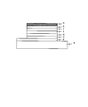
- FIG. 1 shows an example of a multilayered organic EL element.
- the layer responsible for light emission is described as the light emitting layer 1
- the layer in contact with the anode 2 is described as the hole injection layer 3
- the layer in contact with the cathode 4 is described as the electron injection layer 5.
- the layer in contact with the cathode 4 is described as the electron injection layer 5.
- a hole transport layer 6 when a different layer exists between the light emitting layer 1 and the hole injection layer 3, it is described as a hole transport layer 6, and when a different layer exists between the light emitting layer 1 and the electron injection layer 5, an electron transport is described. It is described as layer 7.
- reference numeral 8 denotes a substrate.
- low molecular organic EL elements are formed by vapor deposition, multilayering can be easily achieved by performing vapor deposition while sequentially changing the compounds to be used.
- a polymer type organic EL element forms a film using a wet process such as printing or inkjet, there arises a problem that the lower layer dissolves when the upper layer is applied. For this reason, it is difficult to make a polymer organic EL element multi-layered as compared to a low molecular organic EL element, and it has not been possible to obtain an effect of improving luminous efficiency and life.
- Patent Document 2 discloses an element having a three-layer structure in which a layer called an interlayer is introduced on PEDOT: PSS.
- the present invention produces an organic electronic device having high thermal stability, excellent storage stability when used as an ink composition, and capable of reducing driving voltage and stable driving for a long time with high yield.
- An object of the present invention is to provide an organic electronic material that can be used, and an ink composition containing the organic electronic material. Furthermore, an object of the present invention is to provide an organic electronics element and an organic EL element having a layer having a better charge transport property than conventional ones.
- the present inventors have found that the material of the present invention combining an ionic compound having a specific structure and a compound having a charge transporting unit can solve some of the above problems.
- the present invention has been completed. That is, the present invention is characterized by the following items ⁇ 1> to ⁇ 11>.
- An organic electronic material containing at least an ionic compound represented by the following general formula (1) and a compound having a charge transporting unit (hereinafter referred to as a charge transporting compound).
- R a to R c each independently represent a hydrogen atom (H), an alkyl group, or a benzyl group, and N is not bonded to an aryl group.
- A represents an anion.
- Y 1 to Y 6 are each independently a divalent linking group, and R 1 to R 16 are each independently an electron-withdrawing organic substituent (these structures Further, it may have a substituent or a hetero atom, and R 2 and R 3 , R 4 to R 6 , R 7 to R 10 or R 11 to R 16 are bonded to each other to form a ring or a polymer.
- E 1 represents an oxygen atom
- E 2 represents a nitrogen atom
- E 3 represents a carbon atom
- E 4 represents a boron atom or a gallium atom
- E 5 represents a phosphorus atom or an antimony atom.
- ⁇ 4> The organic electronic material according to any one of ⁇ 1> to ⁇ 3>, wherein the charge transporting compound is a polymer or an oligomer.
- ⁇ 5> The organic electronic material according to any one of ⁇ 1> to ⁇ 4>, wherein the charge transporting compound has one or more polymerizable substituents.
- An ink composition comprising the organic electronic material according to any one of ⁇ 1> to ⁇ 6> and a solvent.
- An organic electronic device comprising a layer formed by a coating method using the organic electronic material according to any one of ⁇ 1> to ⁇ 6> or the ink composition according to ⁇ 7>.
- the organic electronics which can produce the organic electronics element which has high thermal stability, is excellent in storage stability when used as an ink composition, and can reduce the driving voltage and can stably drive for a long time with a high yield.
- Materials and ink compositions comprising the organic electronics materials can be provided.
- the organic electronics element and organic EL element which have a layer excellent in charge transport property compared with the past can be provided.
- Organic electronic material of the present invention is characterized by containing at least an ionic compound represented by the following general formula (1) and a compound having a charge transporting unit (hereinafter referred to as a charge transporting compound).
- R a to R c each independently represent a hydrogen atom (H), an alkyl group, or a benzyl group, and N is not bonded to an aryl group.
- A represents an anion.
- N in the general formula (1) binds to a hydrogen atom (H), an alkyl group, or a benzyl group and does not bind to an aryl group.
- H hydrogen atom
- benzyl group does not bind to an aryl group.
- stability by heat and light is improved.
- the stability of the ink composition containing the compound having the charge transporting unit and the solvent is improved.
- the ionic compound can be used as a polymerization initiator, and a laminated element using a coating method can be produced by combining with a compound having a polymerizable substituent.
- a film formed using the ink composition containing the ionic compound has a high charge transport capability and is useful for organic electronics.
- R a to R c may be the same or different.
- R a to R c may be linked to form a ring.
- the alkyl group in the general formula (1) may be linear, branched or cyclic, and may have a substituent, and usually has about 1 to 20 carbon atoms. Specific examples thereof include methyl Group, ethyl group, propyl group, i-propyl group, butyl group, i-butyl group, t-butyl group, pentyl group, hexyl group, cyclohexyl group, heptyl group, octyl group, 2-ethylhexyl group, nonyl group, decyl Group, undecyl group, dodecyl group, tridecyl group, isotridecyl group, tetradecyl group, pentadecyl group, hexadecyl group, isohexadecyl group, heptadecyl group, octadecyl group, nonadecyl group, icosyl group, 3,
- R a ⁇ R c is an alkyl group or a benzyl group, at least two alkyl group or a benzyl group R a ⁇ R c It is more desirable that R a to R c are all alkyl groups or benzyl groups. In order to improve the thermal stability, it is preferable that all of R a to R c are alkyl groups. In order to improve low-temperature curability as an initiator, it is desirable that at least one of R a to R c is a benzyl group.
- the total number of carbon atoms of R a to R c is preferably 6 or more, more preferably 9 or more, and most preferably 12 or more.
- A is not particularly limited as long as it is a conventionally known anion, but the anions represented by the following general formulas (1b) to (5b) can reduce driving voltage and can be driven stably for a long time It is preferable in manufacturing a simple organic electronics element, particularly an organic EL element.
- Y 1 to Y 6 are each independently a divalent linking group, and R 1 to R 16 are each independently an electron-withdrawing organic substituent (these structures Further, it may have a substituent or a hetero atom, and R 2 and R 3 , R 4 to R 6 , R 7 to R 10 or R 11 to R 16 are bonded to each other to form a ring or a polymer.
- E 1 represents an oxygen atom
- E 2 represents a nitrogen atom
- E 3 represents a carbon atom
- E 4 represents a boron atom or a gallium atom
- E 5 represents a phosphorus atom or an antimony atom.
- Examples of electron withdrawing organic substituents include halogen atoms such as fluorine atom, chlorine atom and bromine atom, cyano group, thiocyano group, nitro group, mesyl group and the like.
- Carbon number such as alkylsulfonyl group, arylsulfonyl group such as tosyl group, formyl group, acetyl group, benzoyl group, etc. is usually 1-12, preferably 6 or less, such as acyl group, methoxycarbonyl group, ethoxycarbonyl group, etc.
- a group obtained by substituting a part or all of the hydrogen atoms of the group having a hydrogen atom with a halogen atom such as fluorine among the organic groups For example, a linear, branched or cyclic perfluoroalkyl group, perfluoroalkylsulfonyl group, perfluoroaryl group, perfluoroalkyloxysulfonyl group, perfluoroarylsulfonyl group that may contain a heteroatom having 1 to 20 carbon atoms Group, perfluoroaryloxysulfonyl group, perfluoroacyl group, perfluoroalkoxycarbonyl group, perfluoroacyloxy group, perfluoroaryloxycarbonyl group, perfluoroalkenyl group, perfluoroalkynyl group, and the following structural formula group (1 ) But is limited to this Not intended to be.
- linear or branched perfluoroalkyl groups having 1 to 8 carbon atoms, cyclic perfluoroalkyl groups having 3 to 6 carbon atoms, and perfluoroaryl groups having 6 to 18 carbon atoms are preferable.
- Y 1 to Y 6 in the above general formula represent a divalent linking group, and specifically, any one of the following general formulas (1c) to (11c) is preferable.
- R represents an arbitrary organic group (these structures may further have a substituent or a hetero atom).
- R in the general formulas (7c) to (11c) is each independently an alkyl group, an alkenyl group, an alkynyl group, an aromatic group, which may be substituted from the viewpoint of improving electron acceptability and solubility in a solvent. It is preferably a hydrocarbon group or an aromatic heterocyclic group, more preferably an organic group having an electron-withdrawing substituent among the substituents.
- the group of the structural formula group (1) is Can be mentioned.
- the anion in the present invention preferably has a negative charge mainly on an oxygen atom, nitrogen atom, carbon atom, boron atom or gallium atom, and is not particularly limited, but more preferably an oxygen atom, nitrogen atom, carbon atom, boron Most preferred are those represented by the following general formulas (12c), (13c), (14c), and (15c).
- R F1 to R F10 are each independently an electron-withdrawing organic substituent (these structures may further have a substituent or a hetero atom, and R F1 to R F9 are bonded to each other). It may be cyclic or polymeric, and is not particularly limited, and examples thereof include groups represented by the structural formula group (1).
- charge transporting compound in the present invention will be described in detail.
- the charge transporting compound refers to a compound having a charge transporting unit.
- the “charge transporting unit” is an atomic group having the ability to transport holes or electrons, and details thereof will be described below.
- the charge transporting unit is not particularly limited as long as it has an ability to transport holes or electrons, and is preferably an amine having an aromatic ring, carbazole, or thiophene. Specific examples thereof include those described in International Publication No. 2011/132702. Of these, the following amine structures (1) to (14) are particularly preferred. The meanings of E, Ar, and X in the amine structures (1) to (14) below are described in detail in the above-mentioned publication, but are simply as shown below.
- E is independently —R 1 , —OR 2 , —SR 3 , —OCOR 4 , —COOR 5 , —SiR 6 R 7 R 8 (wherein R 1 to R 8 are a hydrogen atom and have 1 to 22 carbon atoms)
- R 1 to R 8 are a hydrogen atom and have 1 to 22 carbon atoms
- Each represents a straight-chain, cyclic or branched alkyl group, or an aryl group or heteroaryl group having 2 to 30 carbon atoms, etc.
- Ar is independently an arylene group having 2 to 30 carbon atoms, or Represents a heteroarylene group.
- the arylene group and heteroaryl group may have a substituent.
- X and Z are each independently a divalent linking group, and are not particularly limited.
- a group obtained by further removing one hydrogen atom from a group having one or more hydrogen atoms in R is preferable.
- x represents an integer of 0-2.
- Y is the trivalent linking group, and represents a group obtained by removing two hydrogen atoms from a group having two or more hydrogen atoms in the R.
- charge transporting compound in the present invention may be a commercially available one, or one synthesized by a method known to those skilled in the art, and is not particularly limited.
- the charge transporting compound in the present invention may be a low molecular compound or a high molecular compound such as a polymer or an oligomer. From the viewpoint of solubility in an organic solvent, a polymer compound such as a polymer or an oligomer is preferable, and from the viewpoint of easy purification by sublimation or recrystallization, a low molecular compound is preferable.
- the charge transporting compound in the present invention is a polymer or oligomer
- a polymer or oligomer having a structure branched in three or more directions is preferable from the viewpoint of lowering the temperature for allowing sufficient polymerization reaction to proceed.
- this branched structure can raise the glass transition temperature of a polymer or an oligomer, and contributes also to the heat resistance improvement of a polymer or an oligomer.
- This branched structure is the same as the degree of polymerization relative to the main chain when the main chain has the highest degree of polymerization among the various chains in a polymer or oligomer molecule.
- the degree of polymerization represents the number of monomer units used in synthesizing a polymer or oligomer per molecule of the polymer or oligomer.
- the side chain is a chain that is different from the main chain of the polymer or oligomer and has at least one polymer unit, and the other side chain is regarded as a substituent instead of a side chain.
- a polymer or oligomer may be formed using a monomer having three or more polymerizable sites in one molecule, or after forming a linear polymer or oligomer, It may be formed by polymerizing each other, and is not particularly limited.
- any one of the structures represented by the following general formulas (1) to (10) is included as a starting unit for forming a branched structure in the polymer or oligomer.
- each Ar independently represents a divalent linking group, and represents an arylene group having 2 to 30 carbon atoms or a heteroarylene group.
- the arylene group excludes two hydrogen atoms from an aromatic hydrocarbon. And may have a substituent, such as phenylene, biphenyl-diyl, terphenyl-diyl, naphthalene-diyl, anthracene-diyl, tetracene-diyl, fluorene-diyl, phenanthrene-diyl, etc.
- a heteroarylene group is an atomic group obtained by removing two hydrogen atoms from an aromatic compound having a hetero atom, and may have a substituent, such as pyridine-diyl, pyrazine-diyl, quinoline-diyl.
- Y is preferably a divalent linking group represented by the following formula.
- each R independently represents a hydrogen atom, a linear, cyclic or branched alkyl group having 1 to 22 carbon atoms, or an aryl group or heteroaryl group having 2 to 30 carbon atoms.
- a heteroaryl group is a compound obtained by removing one hydrogen atom from an aromatic compound having a heteroatom. (It is an atomic group and may have a substituent.)
- the charge transporting compound in the present invention preferably has one or more “polymerizable substituents” in order to produce a laminated structure of an organic thin film by changing the solubility.
- the “polymerizable substituent” means a substituent capable of forming a bond between two or more molecules by causing a polymerization reaction, and details thereof will be described below.
- Examples of the polymerizable substituent include a group having a carbon-carbon multiple bond (for example, vinyl group, acetylene group, butenyl group, acrylic group, acrylate group, acrylamide group, methacryl group, methacrylate group, methacrylamide group, arene group).
- a group having a carbon-carbon multiple bond for example, vinyl group, acetylene group, butenyl group, acrylic group, acrylate group, acrylamide group, methacryl group, methacrylate group, methacrylamide group, arene group.
- combinations of groups capable of forming an ester bond or an amide bond can also be used. For example, a combination of an ester group and an amino group, an ester group and a hydroxyl group, or the like.
- an oxetane group, an epoxy group, a vinyl group, a vinyl ether group, an acrylate group, and a methacrylate group are particularly preferable from the viewpoint of reactivity, and an oxetane group is most preferable.
- the main chain of the polymer or oligomer and the polymerizable substituent are connected by an alkyl chain having 1 to 8 carbon atoms. preferable.
- the polymer or oligomer in the present invention is represented by the general formulas (1a) to (84a) described in the aforementioned International Publication No. 2011/132702 in order to adjust the solubility, heat resistance, and electrical characteristics.
- a copolymer having a structure represented by the following structural formula group (X) as the above-described arylene group or heteroarylene group as a copolymer repeating unit may be used.
- the copolymer may be a random, block or graft copolymer, or may be a polymer having an intermediate structure thereof, for example, a random copolymer having a block property.
- each R in the structural formula group (X) independently represents a hydrogen atom, a linear, cyclic or branched alkyl group having 1 to 22 carbon atoms, or an aryl group or heteroaryl group having 2 to 30 carbon atoms. .
- the charge transporting compound is a polymer or oligomer
- the number average molecular weight is preferably 1,000 or more and 1,000,000 or less from the viewpoint of solubility in a solvent and film-forming property. More preferably, it is 2,000 or more and 900,000 or less, and further preferably 3,000 or more and 800,000 or less. If it is less than 1,000, the compound is easily crystallized, resulting in poor film-forming properties. On the other hand, if it is larger than 1,000,000, the solubility in a solvent is lowered, making it difficult to produce a coating solution or a coating ink.
- the organic electronic material of the present invention preferably contains a polymerization initiator in order to utilize the difference in solubility due to the polymerization reaction.
- the polymerization initiator is not particularly limited as long as it exhibits the ability to polymerize a polymerizable substituent by application of heat, light, microwave, radiation, electron beam, and the like. Or it is preferable to start polymerization by heating.
- the ionic compound according to the present invention can be used alone as a polymerization initiator.
- a solution (ink composition) containing the organic electronics material of the present invention is used, for example, an inkjet method.
- Coating method, dipping method, letterpress printing, intaglio printing, offset printing, flat plate printing, letterpress inversion offset printing, screen printing, gravure printing, and other known methods such as spin coating, and coating on a desired substrate it can carry out by making the polymerization reaction of a polymer or an oligomer advance by light irradiation or heat treatment, and changing (curing) the solubility of the coating layer. By repeating such operations, it is possible to increase the number of polymer organic electronics elements and organic EL elements.
- the coating method as described above can usually be carried out in the temperature range of ⁇ 20 to + 300 ° C., preferably 10 to 100 ° C., particularly preferably 15 to 50 ° C.
- the solvent used in the solution is particularly Although there is no restriction
- a light source such as a low-pressure mercury lamp, a medium-pressure mercury lamp, a high-pressure mercury lamp, an ultrahigh-pressure mercury lamp, a metal halide lamp, a xenon lamp, a fluorescent lamp, a light-emitting diode, or sunlight can be used for the light irradiation.
- the heat treatment can be performed on a hot plate or in an oven, and can be performed at a temperature range of 0 to + 300 ° C., preferably 50 to 250 ° C., particularly preferably 80 to 200 ° C.
- the ink composition of the present invention is characterized by containing the organic electronic material of the present invention described above and a solvent, and other additives such as polymerization inhibitors, stabilizers, thickeners, gelling agents, A flame retardant, an antioxidant, a reduction inhibitor, an oxidant, a reducing agent, a surface modifier, an emulsifier, an antifoaming agent, a dispersant, a surfactant, and the like may be included.
- additives such as polymerization inhibitors, stabilizers, thickeners, gelling agents, A flame retardant, an antioxidant, a reduction inhibitor, an oxidant, a reducing agent, a surface modifier, an emulsifier, an antifoaming agent, a dispersant, a surfactant, and the like may be included.
- the solvent examples include water, alcohols such as methanol, ethanol and isopropyl alcohol, alkanes such as pentane, hexane and octane, cyclic alkanes such as cyclohexane, aromatic solvents such as benzene, toluene, xylene, mesitylene, tetralin and diphenylmethane, ethylene Aliphatic ethers such as glycol dimethyl ether, ethylene glycol diethyl ether, propylene glycol-1-monomethyl ether acetate, 1,2-dimethoxybenzene, 1,3-dimethoxybenzene, anisole, phenetole, 2-methoxytoluene, 3-methoxytoluene , 4-methoxytoluene, 2,3-dimethylanisole, aromatic ethers such as 2,4-dimethylanisole, ethyl acetate, n-butyl acetate,
- Amide solvents others, dimethyl sulfoxide, tetrahydrofuran, acetone, chloroform, methylene chloride and the like can be mentioned, but preferably aromatic solvents, aliphatic esters, aromatic esters, aliphatic ethers, aromatic ethers can be used. .
- the content of the organic electronic material with respect to the solvent is preferably 0.1 to 30% by mass from the viewpoint of being applicable to various coating processes.
- the organic electronics element of the present invention includes a layer formed by a coating method using the organic electronic material or the ink composition, and a layer obtained by polymerizing the formed layer and insolubilizing the layer.
- the organic electroluminescent element (organic EL element) of the present invention is a layer formed using the organic electronic material or the ink composition, and a layer obtained by polymerizing the formed layer and insolubilizing the layer. including.
- Each element includes an excellent layer formed using the organic electronic material of the present invention, has a driving voltage lower than that of the prior art, and has a long light emission lifetime.
- the EL element of the present invention will be described in detail below.
- the organic EL device of the present invention is not particularly limited as long as it includes a light emitting layer, a polymerized layer, an anode, a cathode, and a substrate. Other elements such as a hole injection layer, an electron injection layer, a hole transport layer, and an electron transport layer are used. It may have a layer.
- the hole injection layer, the hole transport layer, or the light emitting layer is preferably a layer formed using the organic electronic material or ink composition of the present invention.
- each layer will be described in detail.
- the material used for the light emitting layer may be a low molecular compound, a polymer or an oligomer, and a dendrimer or the like can also be used.
- low molecular weight compounds that utilize fluorescence include perylene, coumarin, rubrene, quinacudrine, dye laser dyes (eg, rhodamine, DCM1, etc.), aluminum complexes (eg, Tris (8-hydroxyquinolinato) aluminum (III) (Alq 3 )), Stilbene, and derivatives thereof.
- Polymers or oligomers that utilize fluorescence include polyfluorene, polyphenylene, polyphenylene vinylene (PPV), polyvinyl carbazole (PVK), fluorene-benzothiadiazole copolymer, fluorene-triphenylamine copolymer, and derivatives thereof And a mixture can be suitably used.
- phosphorescent organic EL devices have been actively developed in order to increase the efficiency of organic EL devices.
- the phosphorescent organic EL element not only singlet state energy but also triplet state energy can be used, and the internal quantum yield can be increased to 100% in principle.
- phosphorescence is emitted by doping a host material with a metal complex phosphorescent material containing a heavy metal such as platinum or iridium as a dopant that emits phosphorescence (MABaldo et al., Nature, vol. 395). , p. 151 (1998), MABaldo et al., Applied Physics Letters, vol.75, p.4 (1999), MABaldo et al., Nature, vol.403, p.750 (2000)). .
- a phosphorescent material for the light emitting layer from the viewpoint of high efficiency.
- a metal complex containing a central metal such as Ir or Pt can be preferably used.
- Ir complex for example, FIr (pic) that emits blue light [iridium (III) bis [(4,6-difluorophenyl) -pyridinate-N, C 2 ] picolinate], green light is emitted.
- Ir (ppy) 3 [Factris (2-phenylpyridine) iridium] (see MABaldo et al., Nature, vol. 403, p.
- Pt complex examples include 2,3,7,8,12,13,17, 18-octaethyl-21H, 23H-forminplatinum (PtOEP) that emits red light.
- PtOEP 23H-forminplatinum
- the phosphorescent material can be a small molecule or a dendrite species, such as an iridium nucleus dendrimer. Moreover, these derivatives can also be used conveniently.
- a host material is included in addition to the phosphorescent material.
- the host material may be a low molecular compound or a high molecular compound, and a dendrimer or the like can also be used.
- low molecular weight compound examples include CBP (4,4′-Bis (Carbazol-9-yl) -biphenyl), mCP (1,3-bis (9-carbazolyl) benzene), CDBP (4,4′-Bis).
- Carbazol-9-yl) -2,2′-dimethylbiphenyl and the like, for example, polyvinyl carbazole, polyphenylene, polyfluorene, etc. can be used as the polymer compound, and derivatives thereof can also be used.
- the light emitting layer may be formed by a vapor deposition method or a coating method.
- a solution containing a phosphorescent material and, if necessary, a host material is used, for example, an ink jet method, a casting method, a dipping method, a relief printing, an intaglio printing, an offset printing, a flat printing, a relief printing. It can be carried out by applying on a desired substrate by a known method such as a printing method such as reverse offset printing, screen printing or gravure printing, or spin coating method.
- the cathode material is preferably a metal or metal alloy such as Li, Ca, Mg, Al, In, Cs, Ba, Mg / Ag, LiF, and CsF.
- anode As the anode, a metal (for example, Au) or other material having metal conductivity, for example, an oxide (for example, ITO: indium oxide / tin oxide), a conductive polymer (for example, a polythiophene-polystyrene sulfonic acid mixture (for example, PEDOT: PSS)) can also be used.
- a metal for example, Au
- an oxide for example, ITO: indium oxide / tin oxide
- a conductive polymer for example, a polythiophene-polystyrene sulfonic acid mixture (for example, PEDOT: PSS)
- PEDOT polythiophene-polystyrene sulfonic acid mixture
- Electrode transport layer electron injection layer
- the electron transport layer and the electron injection layer include phenanthroline derivatives (for example, 2,9-dimethyl-4,7-diphenyl-1,10-phenanthroline (BCP)), bipyridine derivatives, nitro-substituted fluorene derivatives, diphenylquinone derivatives.
- Thiopyran dioxide derivatives such as naphthaleneperylene, carbodiimide, fluorenylidenemethane derivatives, anthraquinodimethane and anthrone derivatives, oxadiazole derivatives (2- (4-Biphenylyl) -5- (4-tert-butylphenyl-1,3,4-oxadiazole) (PBD)), aluminum complexes (for example, Tris (8-hydroxyquinolinato) aluminum (III) (Alq 3 )) and the like.
- a thiadiazole derivative in which the oxygen atom of the oxadiazole ring is substituted with a sulfur atom, or a quinoxaline derivative having a quinoxaline ring known as an electron withdrawing group can be used.
- the kind of glass, plastic and the like is not particularly limited, and is not particularly limited as long as it is transparent, but glass, quartz, light transmissive A resin film or the like is preferably used.
- a resin film flexible substrate
- the resin film examples include polyethylene terephthalate (PET), polyethylene naphthalate (PEN), polyethersulfone (PES), polyetherimide, polyetheretherketone, polyphenylene sulfide, polyarylate, polyimide, polycarbonate (PC), and cellulose triacetate.
- PET polyethylene terephthalate
- PEN polyethylene naphthalate
- PES polyethersulfone
- CAP cellulose acetate propionate
- the resin film may be coated with an inorganic substance such as silicon oxide or silicon nitride in order to suppress permeation of water vapor or oxygen.
- the emission color in the organic EL device of the present invention is not particularly limited, but the white light-emitting device is preferable because it can be used for various lighting devices such as home lighting, interior lighting, clocks, and liquid crystal backlights.
- a plurality of light emitting colors can be simultaneously emitted and mixed using a plurality of light emitting materials.
- White luminescence is obtained.
- a combination of a plurality of emission colors is not particularly limited. However, a combination of three emission maximum wavelengths of blue, green, and red, a complementary color relationship such as blue and yellow, yellow green and orange is used. The thing containing two light emission maximum wavelengths is mentioned. The emission color can be controlled by adjusting the type and amount of the phosphorescent material.
- the display element of the present invention is characterized by including the above-described organic EL element of the present invention.
- a color display element can be obtained by using the organic EL element of the present invention as an element corresponding to each pixel of red, green, and blue (RGB).
- Image formation includes a simple matrix type in which individual organic EL elements arranged in a panel are directly driven by electrodes arranged in a matrix, and an active matrix type in which thin film transistors are arranged and driven in each element.
- the former is simple in structure but has a limit on the number of vertical pixels and is used for displaying characters.
- the latter is used for high-quality displays because the drive voltage is low and the current is small, and a bright high-definition image is obtained.
- the lighting device of the present invention is characterized by including the organic EL element of the present invention described above. Furthermore, the display device of the present invention is characterized by including a lighting device and a liquid crystal element as a display means.
- the illumination device of the present invention described above may be used as a backlight (white light source), and a display device using a liquid crystal element as a display unit, that is, a liquid crystal display device may be used.
- This configuration is a configuration in which only the backlight is replaced with the illumination device of the present invention in a known liquid crystal display device, and a known technique can be diverted to the liquid crystal element portion.
- Example 1 Evaluation of curability
- Polymer 1 (5.0 mg) and ionic compound 1 (0.15 mg) were dissolved in a chlorobenzene solution (1000 ⁇ l) to prepare an ink composition.
- This ink composition was spin-coated on a quartz plate at 3000 rpm.
- the polymerization reaction was performed by heating at 180 ° C. for 10 minutes on a hot plate. After heating, the quartz plate was immersed in toluene for 1 minute for cleaning.
- the residual film ratio was measured from the ratio of absorbance (Abs) of the absorption maximum ( ⁇ max) in the UV-vis spectrum before and after washing. The measurement results are shown in Table 1.
- an evaluation element was produced as follows. ⁇ Production of charge transportability evaluation element> A mixed solution of polymer 1 (100 mg), the ionic compound 1 (3.0 mg), and anisole (1.91 mL) was spin-coated at 3000 min ⁇ 1 on a glass substrate patterned with ITO to a width of 1.6 mm, and a hot plate A charge transport film (150 nm) was produced by heating at 180 ° C. for 10 minutes. Next, the obtained glass substrate was moved into a vacuum evaporation machine, and aluminum (film thickness 100 nm) was evaporated.
- the substrate After vapor deposition of aluminum, the substrate is moved into a dry nitrogen environment without opening to the atmosphere, and the sealing glass and ITO substrate in which 0.4 mm of counterbore is put into 0.7 mm non-alkali glass are used as a photocurable epoxy resin. Sealing was performed by laminating using, to produce a charge transporting evaluation element.
- a voltage was applied using ITO as a positive electrode and aluminum as a cathode of these charge transportability evaluation elements.
- Table 1 shows the applied voltage at 50 mA / cm 2 energization.
- Example 2 In Example 1, except that the ionic compound 1 was changed to the ionic compounds 2 to 10, an ink composition was prepared in the same manner as in Example 1, and the curability, ink stability, and charge transport property were evaluated. The evaluation results are shown in Table 1.
- Example 1 In Example 1, except that the ionic compound 1 was changed to the following ionic compound, an ink composition was prepared in the same manner as in Example 1, and the curability, ink stability, and charge transportability were evaluated. The evaluation results are shown in Table 1.
- Example 2 In Example 1, except that the ionic compound 1 was changed to the following ionic compound, an ink composition was prepared in the same manner as in Example 1, and the curability, ink stability, and charge transportability were evaluated. The evaluation results are shown in Table 1.
- Example 3 an ink composition was prepared in the same manner as in Example 1 except that the ionic compound 1 was not added, and the curability, ink stability, and charge transport property were evaluated. The evaluation results are shown in Table 1.
- Example 8 (Preparation of organic EL element 1) A coating solution in which the polymer 1 (10 mg) obtained above, the ionic compound 1 (0.3 mg), and chlorobenzene (1000 ⁇ l) were mixed on a glass substrate patterned with ITO to a width of 1.6 mm was spun at 3000 min ⁇ 1 . After coating, it was cured by heating on a hot plate at 180 ° C. for 10 minutes to form a hole injection layer (30 nm).
- the obtained glass substrate was transferred into a vacuum vapor deposition machine, ⁇ NPD (40 nm), ( ⁇ NPD + Ir (piq) 3 (5: 1, 20 nm), BAlq (10 nm), Alq 3 (40 nm), LiF (film thickness 0). .5 nm) and Al (film thickness 100 nm) in this order.
- the substrate is moved into a dry nitrogen environment without opening to the atmosphere, and the sealing glass and ITO substrate in which 0.4 mm of counterbore is added to 0.7 mm non-alkali glass are coated with a photocurable epoxy resin. Sealing was performed by using them together to produce a polymer organic EL device having a multilayer structure.
- the luminance was measured with Topcon BM-7 while applying a constant current, and the time for the luminance to halve from the initial luminance (3000 cd / m 2 ) was measured and found to be 420 hours.
- Example 4 An organic EL device was produced in the same manner as in Example 8 except that the ionic compound 1 was changed to the ionic compound used in Comparative Example 1. Red light emission was observed at 6.2 V, and the current efficiency at a luminance of 1000 cd / m 2 was 1.1 cd / A. In addition, as a lifetime characteristic, luminance was measured with Topcon BM-7 while applying a constant current, and the time for the luminance to halve from the initial luminance (3000 cd / m 2 ) was measured and found to be 6 hours.
- Example 9 (Preparation of organic EL element 2) A coating solution in which the polymer 1 (10 mg) obtained above, the ionic compound 10 (0.3 mg), and toluene (1000 ⁇ l) were mixed on a glass substrate patterned with ITO to a width of 1.6 mm was spun at 3000 min ⁇ 1 . After coating, it was cured by heating on a hot plate at 180 ° C. for 10 minutes to form a hole injection layer (30 nm). Next, the obtained glass substrate was transferred into a vacuum evaporation machine, ⁇ NPD (50 nm), CBP + Ir (ppy) 3 (100: 6, 30 nm), BAlq (10 nm), Alq 3 (30 nm), LiF (film thickness 0.
- the substrate is moved into a dry nitrogen environment without opening to the atmosphere, and the sealing glass and ITO substrate in which 0.4 mm of counterbore is added to 0.7 mm non-alkali glass are coated with a photocurable epoxy resin. Sealing was performed by using them together to produce a polymer organic EL device having a multilayer structure. Subsequent experiments were performed in the atmosphere at room temperature (25 ° C.).
- Table 2 shows that the ionic compound used for the organic electronic material of the present invention is excellent in heat resistance. By improving the thermal stability, it is expected that deterioration of the material due to baking and damage to the manufacturing apparatus due to volatiles will be suppressed, and high-performance organic EL elements can be manufactured with high yield.
Priority Applications (8)
| Application Number | Priority Date | Filing Date | Title |
|---|---|---|---|
| KR1020167007322A KR101716100B1 (ko) | 2011-11-30 | 2012-11-29 | 유기 일렉트로닉스 재료, 잉크 조성물 및 유기 일렉트로닉스 소자 |
| KR1020147017662A KR101722302B1 (ko) | 2011-11-30 | 2012-11-29 | 유기 일렉트로닉스 재료, 잉크 조성물 및 유기 일렉트로닉스 소자 |
| CN201280058862.9A CN103975455B (zh) | 2011-11-30 | 2012-11-29 | 有机电子材料、油墨组合物以及有机电子元件 |
| JP2013547211A JP5924348B2 (ja) | 2011-11-30 | 2012-11-29 | 有機エレクトロニクス材料、インク組成物、及び有機エレクトロニクス素子 |
| EP12853562.2A EP2787550B1 (en) | 2011-11-30 | 2012-11-29 | Organic electronic material, ink composition, and organic electronic element |
| US14/361,783 US9337429B2 (en) | 2011-11-30 | 2012-11-29 | Organic electronic material, ink composition, and organic electronic element |
| US15/091,834 US9748488B2 (en) | 2011-11-30 | 2016-04-06 | Organic electronic material, ink composition, and organic electronic element |
| US15/649,049 US9985210B2 (en) | 2011-11-30 | 2017-07-13 | Organic electronic material, ink composition, and organic electronic element |
Applications Claiming Priority (2)
| Application Number | Priority Date | Filing Date | Title |
|---|---|---|---|
| JP2011-262034 | 2011-11-30 | ||
| JP2011262034 | 2011-11-30 |
Related Child Applications (2)
| Application Number | Title | Priority Date | Filing Date |
|---|---|---|---|
| US14/361,783 A-371-Of-International US9337429B2 (en) | 2011-11-30 | 2012-11-29 | Organic electronic material, ink composition, and organic electronic element |
| US15/091,834 Division US9748488B2 (en) | 2011-11-30 | 2016-04-06 | Organic electronic material, ink composition, and organic electronic element |
Publications (1)
| Publication Number | Publication Date |
|---|---|
| WO2013081052A1 true WO2013081052A1 (ja) | 2013-06-06 |
Family
ID=48535501
Family Applications (1)
| Application Number | Title | Priority Date | Filing Date |
|---|---|---|---|
| PCT/JP2012/080922 WO2013081052A1 (ja) | 2011-11-30 | 2012-11-29 | 有機エレクトロニクス材料、インク組成物、及び有機エレクトロニクス素子 |
Country Status (7)
| Country | Link |
|---|---|
| US (3) | US9337429B2 (ko) |
| EP (1) | EP2787550B1 (ko) |
| JP (1) | JP5924348B2 (ko) |
| KR (2) | KR101722302B1 (ko) |
| CN (1) | CN103975455B (ko) |
| TW (1) | TWI618689B (ko) |
| WO (1) | WO2013081052A1 (ko) |
Cited By (23)
| Publication number | Priority date | Publication date | Assignee | Title |
|---|---|---|---|---|
| JP2017059745A (ja) * | 2015-09-18 | 2017-03-23 | 日立化成株式会社 | 有機エレクトロニクス材料、有機エレクトロニクス素子、及び有機エレクトロルミネセンス素子 |
| WO2017188023A1 (ja) | 2016-04-28 | 2017-11-02 | 日立化成株式会社 | 電荷輸送性材料及びその利用 |
| JP2017218426A (ja) * | 2016-06-08 | 2017-12-14 | 日立化成株式会社 | イオン性化合物、有機エレクトロニクス材料、有機エレクトロニクス素子、及び有機エレクトロルミネセンス素子 |
| JP2018011010A (ja) * | 2016-07-15 | 2018-01-18 | 日立化成株式会社 | 電荷輸送性材料、インク組成物、及び有機エレクトロニクス素子 |
| WO2018065357A1 (en) | 2016-10-06 | 2018-04-12 | Merck Patent Gmbh | Materials for organic electroluminescent devices |
| WO2018070019A1 (ja) * | 2016-10-13 | 2018-04-19 | 日立化成株式会社 | 有機エレクトロニクス材料、インク組成物、有機エレクトロニクス素子、及び有機エレクトロニクス素子の製造方法 |
| WO2018077662A1 (en) | 2016-10-31 | 2018-05-03 | Merck Patent Gmbh | Formulation of an organic functional material |
| WO2018095888A1 (en) | 2016-11-25 | 2018-05-31 | Merck Patent Gmbh | Bisbenzofuran-fused 2,8-diaminoindeno[1,2-b]fluorene derivatives and related compounds as materials for organic electroluminescent devices (oled) |
| WO2018114882A1 (de) | 2016-12-22 | 2018-06-28 | Merck Patent Gmbh | Materialien für elektronische vorrichtungen |
| WO2018234220A1 (de) | 2017-06-21 | 2018-12-27 | Merck Patent Gmbh | Materialien für elektronische vorrichtungen |
| WO2019007825A1 (en) | 2017-07-03 | 2019-01-10 | Merck Patent Gmbh | ORGANIC ELECTROLUMINESCENCE DEVICE |
| JP2019507491A (ja) * | 2015-12-24 | 2019-03-14 | ダウ グローバル テクノロジーズ エルエルシー | ポリマー層及びそれを含有する有機電子デバイス |
| WO2019101833A1 (en) | 2017-11-24 | 2019-05-31 | Merck Patent Gmbh | Materials for organic electroluminescent devices |
| WO2019238782A1 (en) | 2018-06-15 | 2019-12-19 | Merck Patent Gmbh | Formulation of an organic functional material |
| CN111876020A (zh) * | 2020-08-06 | 2020-11-03 | 中国科学院长春应用化学研究所 | 一种有机发光材料墨水及其制备方法和喷墨打印方法 |
| JP2021038161A (ja) * | 2019-09-02 | 2021-03-11 | 昭和電工マテリアルズ株式会社 | イオン性化合物、有機エレクトロニクス材料、インク組成物、及び有機エレクトロニクス素子 |
| WO2021180950A1 (en) | 2020-03-13 | 2021-09-16 | Merck Patent Gmbh | Materials for organic electroluminescent devices |
| WO2021213918A1 (en) | 2020-04-21 | 2021-10-28 | Merck Patent Gmbh | Formulation of an organic functional material |
| WO2022017998A1 (en) | 2020-07-22 | 2022-01-27 | Merck Patent Gmbh | Materials for organic electroluminescent devices |
| WO2022112541A1 (en) | 2020-11-30 | 2022-06-02 | Merck Patent Gmbh | Materials for organic electroluminescent devices |
| WO2022214507A1 (en) | 2021-04-09 | 2022-10-13 | Merck Patent Gmbh | Materials for organic electroluminescent devices |
| WO2023139034A1 (en) | 2022-01-20 | 2023-07-27 | Merck Patent Gmbh | Organic electric element with mixed host system |
| WO2023213759A1 (de) | 2022-05-04 | 2023-11-09 | Merck Patent Gmbh | Polymere enthaltend speziell substituierte triarylamin-einheiten sowie elektrolumineszenzvorrichtungen enthaltend diese polymere |
Families Citing this family (8)
| Publication number | Priority date | Publication date | Assignee | Title |
|---|---|---|---|---|
| KR101695139B1 (ko) * | 2011-11-30 | 2017-01-10 | 히타치가세이가부시끼가이샤 | 유기 일렉트로닉스 재료, 잉크 조성물 및 유기 일렉트로닉스 소자 |
| EP2966942A4 (en) * | 2013-03-08 | 2016-12-07 | Hitachi Chemical Co Ltd | TREATMENT SOLUTION CONTAINING ION COMPOUND, ORGANIC ELECTRONIC ELEMENT, AND METHOD FOR MANUFACTURING ORGANIC ELECTRONIC ELEMENT |
| JP6782418B2 (ja) * | 2015-09-10 | 2020-11-11 | 昭和電工マテリアルズ株式会社 | 有機エレクトロニクス材料及びその利用 |
| CN108431985B (zh) * | 2016-01-08 | 2020-06-23 | 日立化成株式会社 | 有机电子材料、有机电子元件及有机电致发光元件 |
| KR102142179B1 (ko) * | 2016-10-10 | 2020-08-06 | 주식회사 엘지화학 | 잉크젯용 적외선 투과 잉크 조성물, 이를 이용한 베젤 패턴의 형성방법, 이에 따라 제조한 베젤 패턴 및 이를 포함하는 디스플레이 기판 |
| CN111247656B (zh) * | 2017-10-27 | 2023-03-24 | 日立化成株式会社 | 电荷传输性聚合物及有机电子元件 |
| KR102252886B1 (ko) | 2018-11-27 | 2021-05-17 | 주식회사 엘지화학 | 신규한 고분자 및 이를 이용한 유기발광 소자 |
| CN112251072A (zh) * | 2020-09-17 | 2021-01-22 | 北京科技大学 | 一种聚合物稳定液晶材料的高通量喷墨打印制备方法 |
Citations (6)
| Publication number | Priority date | Publication date | Assignee | Title |
|---|---|---|---|---|
| US1298401A (en) * | 1918-04-23 | 1919-03-25 | Harry Ralph Ricardo | Driving mechanism for propellers. |
| JPS59199712A (ja) * | 1983-04-27 | 1984-11-12 | Mitsui Toatsu Chem Inc | 硬化性樹脂組成物 |
| JP2006233162A (ja) | 2004-03-11 | 2006-09-07 | Mitsubishi Chemicals Corp | 電荷輸送膜用組成物及びイオン化合物、それを用いた電荷輸送膜及び有機電界発光素子、並びに、有機電界発光素子の製造方法及び電荷輸送膜の製造方法 |
| JP2007520858A (ja) | 2003-12-19 | 2007-07-26 | ケンブリッジ ディスプレイ テクノロジー リミテッド | 光学装置 |
| WO2011132702A1 (ja) | 2010-04-22 | 2011-10-27 | 日立化成工業株式会社 | 有機エレクトロニクス材料、重合開始剤及び熱重合開始剤、インク組成物、有機薄膜及びその製造方法、有機エレクトロニクス素子、有機エレクトロルミネセンス素子、照明装置、表示素子、並びに表示装置 |
| JP2012126877A (ja) * | 2010-11-24 | 2012-07-05 | Toyo Ink Sc Holdings Co Ltd | 感圧式接着剤組成物、及びそれを用いてなる感圧式接着剤フィルム |
Family Cites Families (5)
| Publication number | Priority date | Publication date | Assignee | Title |
|---|---|---|---|---|
| TW200517469A (en) | 2003-10-30 | 2005-06-01 | Nissan Chemical Ind Ltd | Charge-transporting compound, charge-transporting material, charge-transporting varnish, charge-transporting thin film, and organic electroluminescent device |
| WO2009102027A1 (ja) | 2008-02-15 | 2009-08-20 | Mitsubishi Chemical Corporation | 共役ポリマー、不溶化ポリマー、有機電界発光素子材料、有機電界発光素子用組成物、ポリマーの製造方法、有機電界発光素子、有機elディスプレイ、及び有機el照明 |
| JP5696662B2 (ja) * | 2009-06-01 | 2015-04-08 | 日立化成株式会社 | 有機エレクトロルミネセンス素子、表示素子、照明装置および表示装置 |
| SG10201405425XA (en) | 2009-10-01 | 2014-10-30 | Hitachi Chemical Co Ltd | Material for organic electronics, organic electronic element, organic electroluminescent element, display element using organic electroluminescent element, illuminating device, and display device |
| US9252376B2 (en) * | 2011-09-26 | 2016-02-02 | Hitachi Chemical Company, Ltd. | Composition capable of changing its solubility, hole transport material composition, and organic electronic element using the same |
-
2012
- 2012-11-29 KR KR1020147017662A patent/KR101722302B1/ko active IP Right Grant
- 2012-11-29 EP EP12853562.2A patent/EP2787550B1/en active Active
- 2012-11-29 JP JP2013547211A patent/JP5924348B2/ja active Active
- 2012-11-29 US US14/361,783 patent/US9337429B2/en active Active
- 2012-11-29 WO PCT/JP2012/080922 patent/WO2013081052A1/ja active Application Filing
- 2012-11-29 CN CN201280058862.9A patent/CN103975455B/zh active Active
- 2012-11-29 KR KR1020167007322A patent/KR101716100B1/ko active IP Right Grant
- 2012-11-30 TW TW101145150A patent/TWI618689B/zh active
-
2016
- 2016-04-06 US US15/091,834 patent/US9748488B2/en active Active
-
2017
- 2017-07-13 US US15/649,049 patent/US9985210B2/en active Active
Patent Citations (6)
| Publication number | Priority date | Publication date | Assignee | Title |
|---|---|---|---|---|
| US1298401A (en) * | 1918-04-23 | 1919-03-25 | Harry Ralph Ricardo | Driving mechanism for propellers. |
| JPS59199712A (ja) * | 1983-04-27 | 1984-11-12 | Mitsui Toatsu Chem Inc | 硬化性樹脂組成物 |
| JP2007520858A (ja) | 2003-12-19 | 2007-07-26 | ケンブリッジ ディスプレイ テクノロジー リミテッド | 光学装置 |
| JP2006233162A (ja) | 2004-03-11 | 2006-09-07 | Mitsubishi Chemicals Corp | 電荷輸送膜用組成物及びイオン化合物、それを用いた電荷輸送膜及び有機電界発光素子、並びに、有機電界発光素子の製造方法及び電荷輸送膜の製造方法 |
| WO2011132702A1 (ja) | 2010-04-22 | 2011-10-27 | 日立化成工業株式会社 | 有機エレクトロニクス材料、重合開始剤及び熱重合開始剤、インク組成物、有機薄膜及びその製造方法、有機エレクトロニクス素子、有機エレクトロルミネセンス素子、照明装置、表示素子、並びに表示装置 |
| JP2012126877A (ja) * | 2010-11-24 | 2012-07-05 | Toyo Ink Sc Holdings Co Ltd | 感圧式接着剤組成物、及びそれを用いてなる感圧式接着剤フィルム |
Non-Patent Citations (5)
| Title |
|---|
| ADACHI ET AL., APPL. PHYS. LETT., vol. 78, no. 11, 2001, pages 1622 |
| M. A. BALDO ET AL., APPLIED PHYSICS LETTERS, vol. 75, 1999, pages 4 |
| M. A. BALDO ET AL., NATURE, vol. 395, 1998, pages 151 |
| M. A. BALDO ET AL., NATURE, vol. 403, 2000, pages 750 |
| See also references of EP2787550A4 |
Cited By (26)
| Publication number | Priority date | Publication date | Assignee | Title |
|---|---|---|---|---|
| JP2017059745A (ja) * | 2015-09-18 | 2017-03-23 | 日立化成株式会社 | 有機エレクトロニクス材料、有機エレクトロニクス素子、及び有機エレクトロルミネセンス素子 |
| JP2019507491A (ja) * | 2015-12-24 | 2019-03-14 | ダウ グローバル テクノロジーズ エルエルシー | ポリマー層及びそれを含有する有機電子デバイス |
| WO2017188023A1 (ja) | 2016-04-28 | 2017-11-02 | 日立化成株式会社 | 電荷輸送性材料及びその利用 |
| JP2017218426A (ja) * | 2016-06-08 | 2017-12-14 | 日立化成株式会社 | イオン性化合物、有機エレクトロニクス材料、有機エレクトロニクス素子、及び有機エレクトロルミネセンス素子 |
| JP2018011010A (ja) * | 2016-07-15 | 2018-01-18 | 日立化成株式会社 | 電荷輸送性材料、インク組成物、及び有機エレクトロニクス素子 |
| WO2018065357A1 (en) | 2016-10-06 | 2018-04-12 | Merck Patent Gmbh | Materials for organic electroluminescent devices |
| WO2018070019A1 (ja) * | 2016-10-13 | 2018-04-19 | 日立化成株式会社 | 有機エレクトロニクス材料、インク組成物、有機エレクトロニクス素子、及び有機エレクトロニクス素子の製造方法 |
| JPWO2018070019A1 (ja) * | 2016-10-13 | 2019-08-15 | 日立化成株式会社 | 有機エレクトロニクス材料、インク組成物、有機エレクトロニクス素子、及び有機エレクトロニクス素子の製造方法 |
| WO2018077662A1 (en) | 2016-10-31 | 2018-05-03 | Merck Patent Gmbh | Formulation of an organic functional material |
| WO2018095888A1 (en) | 2016-11-25 | 2018-05-31 | Merck Patent Gmbh | Bisbenzofuran-fused 2,8-diaminoindeno[1,2-b]fluorene derivatives and related compounds as materials for organic electroluminescent devices (oled) |
| WO2018114882A1 (de) | 2016-12-22 | 2018-06-28 | Merck Patent Gmbh | Materialien für elektronische vorrichtungen |
| WO2018234220A1 (de) | 2017-06-21 | 2018-12-27 | Merck Patent Gmbh | Materialien für elektronische vorrichtungen |
| WO2019007825A1 (en) | 2017-07-03 | 2019-01-10 | Merck Patent Gmbh | ORGANIC ELECTROLUMINESCENCE DEVICE |
| WO2019101833A1 (en) | 2017-11-24 | 2019-05-31 | Merck Patent Gmbh | Materials for organic electroluminescent devices |
| US11939339B2 (en) | 2017-11-24 | 2024-03-26 | Merck Patent Gmbh | Materials for organic electroluminescent devices |
| WO2019238782A1 (en) | 2018-06-15 | 2019-12-19 | Merck Patent Gmbh | Formulation of an organic functional material |
| JP2021038161A (ja) * | 2019-09-02 | 2021-03-11 | 昭和電工マテリアルズ株式会社 | イオン性化合物、有機エレクトロニクス材料、インク組成物、及び有機エレクトロニクス素子 |
| JP7363214B2 (ja) | 2019-09-02 | 2023-10-18 | 株式会社レゾナック | イオン性化合物、有機エレクトロニクス材料、インク組成物、及び有機エレクトロニクス素子 |
| WO2021180950A1 (en) | 2020-03-13 | 2021-09-16 | Merck Patent Gmbh | Materials for organic electroluminescent devices |
| WO2021213918A1 (en) | 2020-04-21 | 2021-10-28 | Merck Patent Gmbh | Formulation of an organic functional material |
| WO2022017998A1 (en) | 2020-07-22 | 2022-01-27 | Merck Patent Gmbh | Materials for organic electroluminescent devices |
| CN111876020A (zh) * | 2020-08-06 | 2020-11-03 | 中国科学院长春应用化学研究所 | 一种有机发光材料墨水及其制备方法和喷墨打印方法 |
| WO2022112541A1 (en) | 2020-11-30 | 2022-06-02 | Merck Patent Gmbh | Materials for organic electroluminescent devices |
| WO2022214507A1 (en) | 2021-04-09 | 2022-10-13 | Merck Patent Gmbh | Materials for organic electroluminescent devices |
| WO2023139034A1 (en) | 2022-01-20 | 2023-07-27 | Merck Patent Gmbh | Organic electric element with mixed host system |
| WO2023213759A1 (de) | 2022-05-04 | 2023-11-09 | Merck Patent Gmbh | Polymere enthaltend speziell substituierte triarylamin-einheiten sowie elektrolumineszenzvorrichtungen enthaltend diese polymere |
Also Published As
| Publication number | Publication date |
|---|---|
| JPWO2013081052A1 (ja) | 2015-04-27 |
| TWI618689B (zh) | 2018-03-21 |
| JP5924348B2 (ja) | 2016-05-25 |
| EP2787550A1 (en) | 2014-10-08 |
| EP2787550A4 (en) | 2015-09-16 |
| CN103975455B (zh) | 2016-08-17 |
| KR20140106617A (ko) | 2014-09-03 |
| KR101722302B1 (ko) | 2017-03-31 |
| US9337429B2 (en) | 2016-05-10 |
| CN103975455A (zh) | 2014-08-06 |
| US20170309824A1 (en) | 2017-10-26 |
| TW201331162A (zh) | 2013-08-01 |
| US20160218290A1 (en) | 2016-07-28 |
| KR101716100B1 (ko) | 2017-03-13 |
| EP2787550B1 (en) | 2020-12-23 |
| US9985210B2 (en) | 2018-05-29 |
| US9748488B2 (en) | 2017-08-29 |
| US20140332791A1 (en) | 2014-11-13 |
| KR20160037242A (ko) | 2016-04-05 |
Similar Documents
| Publication | Publication Date | Title |
|---|---|---|
| US9985210B2 (en) | Organic electronic material, ink composition, and organic electronic element | |
| JP6202075B2 (ja) | 有機エレクトロニクス材料、インク組成物、及び有機エレクトロニクス素子 | |
| JP6331462B2 (ja) | 有機エレクトロニクス素子の製造方法 | |
| WO2016076375A1 (ja) | 有機エレクトロルミネセンス素子及びその製造方法 | |
| JPWO2015122464A1 (ja) | ポリマー又はオリゴマー、正孔輸送材料組成物、及び、これらを用いた有機エレクトロニクス素子 | |
| JP5678552B2 (ja) | 重合開始剤及び有機エレクトロニクス材料、これらを用いた有機薄膜及びその製造方法、インク組成物、有機エレクトロニクス素子、有機エレクトロルミネセンス素子、照明装置、表示素子、並びに表示装置 | |
| JP6136366B2 (ja) | 有機エレクトロニクス素子及びその製造方法 | |
| JP6613561B2 (ja) | 有機エレクトロニクス材料及び有機エレクトロニクス素子 | |
| JP6089389B2 (ja) | 電子受容性化合物及びその製造方法、該化合物を含む重合開始剤、有機エレクトロニクス材料及びこれらを用いた有機薄膜、有機エレクトロニクス素子、有機エレクトロルミネセンス素子、表示素子、照明装置、並びに表示装置 | |
| JP6221230B2 (ja) | 有機エレクトロニクス素子及びその製造方法 | |
| JP6733737B2 (ja) | 有機エレクトロニクス材料、インク組成物、有機エレクトロニクス素子、及び有機エレクトロニクス素子の製造方法 | |
| WO2017212560A1 (ja) | 有機エレクトロニクス材料及び有機エレクトロニクス素子 |
Legal Events
| Date | Code | Title | Description |
|---|---|---|---|
| 121 | Ep: the epo has been informed by wipo that ep was designated in this application |
Ref document number: 12853562 Country of ref document: EP Kind code of ref document: A1 |
|
| ENP | Entry into the national phase |
Ref document number: 2013547211 Country of ref document: JP Kind code of ref document: A |
|
| NENP | Non-entry into the national phase |
Ref country code: DE |
|
| WWE | Wipo information: entry into national phase |
Ref document number: 14361783 Country of ref document: US |
|
| ENP | Entry into the national phase |
Ref document number: 20147017662 Country of ref document: KR Kind code of ref document: A |