WO2013065672A1 - Esd保護デバイス - Google Patents
Esd保護デバイス Download PDFInfo
- Publication number
- WO2013065672A1 WO2013065672A1 PCT/JP2012/078009 JP2012078009W WO2013065672A1 WO 2013065672 A1 WO2013065672 A1 WO 2013065672A1 JP 2012078009 W JP2012078009 W JP 2012078009W WO 2013065672 A1 WO2013065672 A1 WO 2013065672A1
- Authority
- WO
- WIPO (PCT)
- Prior art keywords
- discharge
- protection device
- esd protection
- facing
- conductor
- Prior art date
Links
Images


Classifications
-
- H—ELECTRICITY
- H02—GENERATION; CONVERSION OR DISTRIBUTION OF ELECTRIC POWER
- H02H—EMERGENCY PROTECTIVE CIRCUIT ARRANGEMENTS
- H02H9/00—Emergency protective circuit arrangements for limiting excess current or voltage without disconnection
- H02H9/04—Emergency protective circuit arrangements for limiting excess current or voltage without disconnection responsive to excess voltage
-
- H—ELECTRICITY
- H01—ELECTRIC ELEMENTS
- H01T—SPARK GAPS; OVERVOLTAGE ARRESTERS USING SPARK GAPS; SPARKING PLUGS; CORONA DEVICES; GENERATING IONS TO BE INTRODUCED INTO NON-ENCLOSED GASES
- H01T4/00—Overvoltage arresters using spark gaps
- H01T4/10—Overvoltage arresters using spark gaps having a single gap or a plurality of gaps in parallel
- H01T4/12—Overvoltage arresters using spark gaps having a single gap or a plurality of gaps in parallel hermetically sealed
-
- H—ELECTRICITY
- H02—GENERATION; CONVERSION OR DISTRIBUTION OF ELECTRIC POWER
- H02H—EMERGENCY PROTECTIVE CIRCUIT ARRANGEMENTS
- H02H9/00—Emergency protective circuit arrangements for limiting excess current or voltage without disconnection
- H02H9/04—Emergency protective circuit arrangements for limiting excess current or voltage without disconnection responsive to excess voltage
- H02H9/044—Physical layout, materials not provided for elsewhere
-
- H—ELECTRICITY
- H05—ELECTRIC TECHNIQUES NOT OTHERWISE PROVIDED FOR
- H05K—PRINTED CIRCUITS; CASINGS OR CONSTRUCTIONAL DETAILS OF ELECTRIC APPARATUS; MANUFACTURE OF ASSEMBLAGES OF ELECTRICAL COMPONENTS
- H05K1/00—Printed circuits
- H05K1/02—Details
- H05K1/0213—Electrical arrangements not otherwise provided for
- H05K1/0254—High voltage adaptations; Electrical insulation details; Overvoltage or electrostatic discharge protection ; Arrangements for regulating voltages or for using plural voltages
- H05K1/0257—Overvoltage protection
- H05K1/0259—Electrostatic discharge [ESD] protection
-
- H—ELECTRICITY
- H05—ELECTRIC TECHNIQUES NOT OTHERWISE PROVIDED FOR
- H05K—PRINTED CIRCUITS; CASINGS OR CONSTRUCTIONAL DETAILS OF ELECTRIC APPARATUS; MANUFACTURE OF ASSEMBLAGES OF ELECTRICAL COMPONENTS
- H05K9/00—Screening of apparatus or components against electric or magnetic fields
- H05K9/0067—Devices for protecting against damage from electrostatic discharge
-
- H—ELECTRICITY
- H05—ELECTRIC TECHNIQUES NOT OTHERWISE PROVIDED FOR
- H05K—PRINTED CIRCUITS; CASINGS OR CONSTRUCTIONAL DETAILS OF ELECTRIC APPARATUS; MANUFACTURE OF ASSEMBLAGES OF ELECTRICAL COMPONENTS
- H05K9/00—Screening of apparatus or components against electric or magnetic fields
- H05K9/0073—Shielding materials
- H05K9/0079—Electrostatic discharge protection, e.g. ESD treated surface for rapid dissipation of charges
Definitions
- the present invention relates to an ESD protection device, and more particularly, to an ESD protection device in which a discharge occurs between opposing portions of a discharge electrode exposed in a cavity formed inside a ceramic multilayer substrate.
- ESD Electro-Static Discharge
- a charged conductive object such as a human body
- another conductive object such as an electronic device
- ESD causes problems such as damage and malfunction of electronic devices. In order to prevent this, it is necessary to prevent an excessive voltage generated during discharge from being applied to the circuit of the electronic device.
- An ESD protection device is used for such an application, and is also called a surge absorbing element or a surge absorber.
- the ESD protection device is disposed, for example, between the signal line of the circuit and the ground (ground). Since the ESD protection device has a structure in which a pair of discharge electrodes are spaced apart from each other, the ESD protection device has a high resistance in a normal use state, and a signal does not flow to the ground side. On the other hand, when an excessive voltage is applied, for example, when static electricity is applied from an antenna of a mobile phone or the like, a discharge is generated between the discharge electrodes of the ESD protection device, and the static electricity can be guided to the ground side. Thereby, a voltage due to static electricity is not applied to a circuit subsequent to the ESD device, and the circuit can be protected.
- the cavity 3 and the discharge electrodes 6 and 8 facing each other with a gap 5 are formed inside the ceramic multilayer substrate 2.
- the discharge electrodes 6 and 8 include opposing portions 7 and 9 formed along the inner surface of the cavity portion 3.
- the discharge electrodes 6 and 8 extend from the cavity 3 to the outer peripheral surface of the ceramic multilayer substrate 2 and are connected to external electrodes 6x and 8x formed outside the ceramic multilayer substrate 2, that is, on the surface of the ceramic multilayer substrate 2. Yes.
- the external electrodes 6x and 8x are used for mounting the ESD protection device 1.
- An auxiliary electrode 4 in which a conductive material is dispersed is formed adjacent to the opposing portions 7 and 9 of the discharge electrodes 6 and 8 and the portion where the interval 5 between the opposing portions 7 and 9 is formed.
- the discharge start voltage can be set by adjusting the distance 5 between the opposing portions 7 and 9 of the discharge electrodes 6 and 8 and the amount and type of the conductive material contained in the auxiliary electrode 4 (for example, Patent Document 1). reference).
- the ESD protection device When the ESD protection device is repeatedly discharged, the opposing portions of the discharge electrodes are melted or peeled off due to heat and impact during discharge, resulting in a large gap between the opposing portions of the discharge electrodes, resulting in a high discharge start voltage. Therefore, the discharge characteristics may be deteriorated.
- the discharge electrode when the discharge electrode is formed by printing a conductive paste, the discharge electrodes 14 and 15 formed along the inner surface of the cavity portion 13 as shown in the cross-sectional view of the main part in FIG.
- the ends of the facing portions 14a and 15a are often formed thin.
- the opposing portion 14a of the discharge electrode 14 on the electron receiving side is peeled off or melted and shortened as shown in the cross-sectional view of the main part of FIG. Since the gap between the opposed portions 14a and 15a tends to be large, the deterioration of the discharge characteristics becomes a more serious problem.
- the ceramic constituting the ceramic multilayer substrate which is the main body of the ESD protection device
- sintering occurs when the glass component diffuses into the thinly formed tip of the opposing portion of the discharge electrode during firing of the ESD protection device.
- the opposite portion of the discharge electrode in the oversintered state is that the metal particles grow larger due to heat during discharge, the metal particles are isolated in a ball shape, so-called spheroidized state, and the discharge gap is substantially increased. Discharge characteristics are likely to deteriorate.
- the auxiliary electrode when the glass component is oversintered, the conductive material particles grow due to heat during discharge, the distance between the conductive material particles increases, and the effect of promoting discharge is reduced. Discharge characteristics are likely to deteriorate.
- the present invention intends to provide an ESD protection device capable of suppressing deterioration of discharge characteristics due to repeated discharge.
- the present invention provides an ESD protection device configured as follows.
- the ESD protection device includes: a) an insulating multilayer substrate in which a plurality of insulating layers are stacked; (b) a cavity formed inside the insulating multilayer substrate; and (c) along an inner surface of the cavity. At least a pair of discharge electrodes formed and having opposing portions facing each other at an interval; (d) an external electrode formed on the surface of the insulating multilayer substrate and connected to the discharge electrode; When viewed through in the stacking direction in which the insulating layers of the insulating multilayer substrate are stacked, the facing direction in which the facing portions of the discharge electrode face each other, or the direction perpendicular to both the stacking direction and the facing direction And a conductor portion formed inside the ceramic multilayer substrate so as to cover at least one of the opposing ends of the opposing portion of the discharge electrode.
- the temperature rise at the facing portion of the discharge electrode is suppressed even when the discharge is repeated. For this reason, it is possible to prevent the discharge characteristics from deteriorating due to the gap between the opposing portions of the discharge electrode becoming large due to the melting of the opposing portions of the discharge electrode due to the heat generated during the discharge or peeling.
- the conductor portion is formed so as to cover at least one of the opposing ends of the opposing portion of the discharge electrode when seen through in the stacking direction.
- the insulating layer of at least one layer of the insulating multilayer substrate is disposed between the conductor portion and the facing portion of the discharge electrode.
- the conductor portion widely covers the opposing portion of the discharge electrode along the opposing tip of the opposing portion of the discharge electrode, and has a large area facing the opposing tip of the opposing portion of the discharge electrode, so that the heat during discharge High effect to escape. Therefore, it is possible to more reliably suppress the deterioration of the discharge characteristics.
- the insulating multilayer substrate is a ceramic multilayer substrate containing a glass component.
- the glass component on the side opposite to the facing portion of the discharge electrode with respect to the conductor portion is prevented from moving toward the facing portion of the discharge electrode by the conductor portion.
- the discharge electrode further includes a discharge auxiliary portion formed in a facing region where the tips of the facing portions of the discharge electrode face each other at a shortest distance and including a dispersed metal material and a semiconductor material.
- the conductor portion is formed so as to cover the facing region when seen through in the stacking direction.
- the metal material and the semiconductor material of the discharge assisting portion are arranged in a state of being dispersed in the opposing region, the electrons easily move, so that a discharge phenomenon occurs efficiently and the discharge characteristics are stabilized.
- the conductor portion can effectively dissipate heat generated in the facing region during discharge.
- the insulating multilayer substrate is a ceramic multilayer substrate containing a glass component
- the glass component on the side opposite to the discharge auxiliary portion with respect to the conductor portion during firing of the ESD protection device is directed toward the discharge auxiliary portion by the conductor portion. Movement is blocked. Thereby, since oversintering of the discharge auxiliary
- the conductor portion is arranged in the stacking direction and on the side opposite to the cavity portion with respect to the facing portion of the discharge electrode.
- the conductor portion can be disposed at a position closer to the facing portion of the discharge electrode, so that heat can be radiated more effectively.
- the insulating multilayer substrate is a ceramic multilayer substrate containing a glass component, the diffusion of the glass component can be more effectively suppressed during firing of the ESD protection device.
- the conductor portion is disposed at a plurality of locations between different insulating layers of the insulating multilayer substrate.
- the conductor portion is disposed on both sides in the stacking direction with respect to the facing portion of the discharge electrode.
- the heat radiation and the suppression of the diffusion of the glass component can be more reliably performed by disposing the conductor portions on both main surface sides of the facing portion of the discharge electrode.
- the conductor portion is electrically connected to the discharge electrode.
- an outer conductor portion formed on the surface of the insulating multilayer substrate is further provided.
- the conductor portion and the outer conductor portion are electrically connected.
- a seal layer that is disposed between the facing portion of the discharge electrode and the insulating layer of the insulating layer substrate, and further suppresses transmission of components contained in the insulating layer of the insulating layer substrate.
- the component contained in the insulating multilayer substrate is less likely to reach the opposing portion of the discharge electrode due to the suppression of the permeation of the seal layer, so the opposing portion of the discharge electrode is affected by the component contained in the insulating multilayer substrate. It is possible to suppress the deterioration of the discharge characteristics.
- the insulating multilayer substrate is a ceramic multilayer substrate containing a glass component, it is possible to suppress deterioration of discharge characteristics due to oversintering of the opposing portion of the discharge electrode and the discharge auxiliary portion due to diffusion of the glass component.
- Example 1-1 It is sectional drawing of an ESD protection device.
- Example 1-1 It is sectional drawing of an ESD protection device.
- Example 1-2 It is principal part sectional drawing of an ESD protection device.
- Example 2-1 It is principal part sectional drawing of an ESD protection device.
- Example 2-2 It is principal part sectional drawing of an ESD protection device.
- Example 3-1 It is principal part sectional drawing of an ESD protection device.
- Example 3-2 It is principal part sectional drawing of an ESD protection device.
- Example 4 It is principal part sectional drawing of an ESD protection device.
- Example 5-1 It is principal part sectional drawing of an ESD protection device.
- Example 5-2 It is principal part sectional drawing of an ESD protection device.
- Example It is principal part sectional drawing of an ESD protection device. (Conventional example)
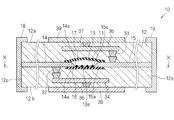
- Example 1-1 An ESD protection device 10 of Example 1-1 will be described with reference to FIGS. 1 and 2.
- FIG. 1 An ESD protection device 10 of Example 1-1 will be described with reference to FIGS. 1 and 2.
- FIG. 1 is a cross-sectional view of the ESD protection device 10.
- FIG. 2 is a cross-sectional view of a principal part taken along line XX in FIG.
- the ESD protection device 10 includes a cavity portion 13 and a pair of discharge electrodes 14 formed inside a ceramic multilayer substrate 12 in which a plurality of ceramic layers are stacked in the vertical direction in FIG. 15.
- the discharge electrodes 14, 15 have opposing portions 14 a, 15 a that are formed along the inner surface of the cavity portion 13, are opposed to each other with an interval, and are exposed in the cavity portion 13.
- External electrodes 18 and 19 are formed on the end faces 12 p and 12 q of the ceramic multilayer substrate 12, and the external electrodes 18 and 19 are connected to the discharge electrodes 14 and 15.
- the external electrodes 18 and 19 are used for mounting the ESD protection device 10 on a circuit board or the like.
- conductor portions 34 and 35 disposed between the ceramic layers of the ceramic multilayer substrate 12 and via conductors 32 and 33; 36 and 37 penetrating the ceramic layers of the ceramic multilayer substrate 12 are provided. Is formed.
- the conductor portions 34 and 35 are connected to the discharge electrodes 14 and 15 via the via conductors 32 and 33.
- the conductor portions 34, 35, the via conductors 32, 33 and the discharge electrodes 14, 15 are conductors that conduct electricity and heat well, and the conductor portions 34, 35 are electrically connected to the discharge electrodes 14, 15.
- External conductor portions 38 and 39 are formed on the upper surface 12 a and the lower surface 12 b of the ceramic multilayer substrate 12.
- the external conductor portions 38 and 39 are connected to the conductor portions 34 and 35 via the via conductors 36 and 37.
- the conductor portions 34, 35, the via conductors 36, 37 and the external conductors 38, 39 are conductors that pass electricity and heat well, and the conductor portions 34, 35 are electrically connected to the external conductors 38, 39.
- Seal layers 16 and 17 are formed between the ceramic multilayer substrate 12 and the cavity 13.
- the sealing layers 16 and 17 are made of ceramics having a higher sintering temperature than the ceramics constituting the ceramic multilayer substrate 12, for example.
- the discharge assisting part 11 includes a dispersed metal material and a semiconductor material.
- assistant part 11 also in the area
- it may be formed on the opposing portions 14a, 15a of the discharge electrodes 14, 15 or between the opposing portions 14a, 15a of the discharge electrodes 14, 15 and the seal layer 16.
- the ESD protection device 10 when a voltage of a predetermined level or more is applied between the external electrodes 18 and 19, the discharge is generated in the cavity 13, that is, between the opposed portions 14 a and 15 a of the discharge electrodes 14 and 15. appear.
- Heat generated at the time of discharge is radiated from the conductor portions 34 and 35 to the outside of the ESD protection device 10 via the via conductors 36 and 37 and the external conductor portions 38 and 39, or from the conductor portions 34 and 35 to the via conductors 32, 33, The heat is radiated to the outside of the ESD protection device 10 through the discharge electrodes 14 and 15 and the external electrodes 18 and 19. By such heat radiation, it is possible to suppress the temperature rise of the facing portions 14a and 15a of the discharge electrodes 14 and 15.
- the opposing portions 14a and 15a of the discharge electrodes 14 and 15 are melted or peeled off due to repeated discharge, whereby the gap between the opposing portions 14a and 15a of the discharge electrodes 14 and 15 is increased, or the ball is turned into a ball and discharged. It can be suppressed that the gap between the opposed portions 14a and 15a of the electrodes 14 and 15 is substantially increased and the discharge characteristics are deteriorated.
- the glass component on the side opposite to the facing portions 14a and 15a of the discharge electrodes 14 and 15 with respect to the conductor portions 34 and 35 is transferred to the discharge electrodes 14 and 15 by the conductor portions 34 and 35. Movement toward the facing portions 14a and 15a and the discharge assisting portion 11 is prevented. This suppresses oversintering of the opposing portions 14a and 15a of the discharge electrodes 14 and 15 and the discharge assisting portion 11 due to the glass component, so It is possible to suppress discharge characteristic deterioration caused by sintering.
- the conductor portions 34 and 35 are disposed at a plurality of positions, that is, on both sides in the stacking direction of the ceramic layers of the ceramic multilayer substrate 12 with respect to the facing portions 14a and 15a of the discharge electrodes 14 and 15, heat dissipation and glass component diffusion suppression are performed. And can be performed more reliably.
- the conductor portions 34 and 35 broadly cover the opposing portions 14a and 15a of the discharge electrodes 14 and 15 along the opposite ends 14s and 15s of the opposing portions 14a and 15a of the discharge electrodes 14 and 15, and are seen through in the stacking direction. It is sometimes formed so as to cover the facing region 13s.
- the conductor portions 34 and 35 have a large area facing the tips 14s and 15s of the facing portions 14a and 15a of the discharge electrodes 14 and 15 that are opposite to each other, and have a high effect of releasing heat during discharge. It can be surely suppressed.
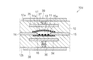
- Example 1-2 An ESD protection device 10a according to Example 1-2 will be described with reference to FIG.
- the ESD protection device 10a of Example 1-2 is configured in substantially the same manner as the ESD protection device 10 of Example 1-1.
- the same reference numerals are used for the same components as in the embodiment 1-1, and the description will focus on the differences from the embodiment 1-1.
- FIG. 3 is a cross-sectional view of the main part of the ESD protection device 10a.
- the ESD protection device 10a includes conductor portions 34a and 35a, external conductor portions 38a and 39a, and via conductors 32a arranged between the ceramic layers of the ceramic multilayer substrate 12 in the same manner as in Example 1-1.
- 33a; 36a, 37a, both of which are arranged on one side of the cavity 13, that is, on the opposite side of the cavity 13 in the stacking direction with respect to the opposing parts 14a, 15a of the discharge electrodes 14, 15. Yes.
- the conductor portions 34a and 35a are connected to the discharge electrodes 14 and 15 via the via conductors 32a and 33a, and are connected to the external conductor portions 38a and 39a via the via conductors 36a and 37a. Since the outer conductor portions 38a and 39a are sufficiently separated from each other, no discharge occurs between the outer conductor portions 38a and 39a.
- the conductor portions 34a and 35a are connected to the facing portions 14a of the discharge electrodes 14 and 15. , 15a to dissipate heat more effectively. Moreover, diffusion of the glass component can be more effectively suppressed. Since the conductor portions 34a and 35a are provided at a plurality of locations, it is possible to more reliably perform heat dissipation and suppression of glass component diffusion. Therefore, it is possible to suppress deterioration of discharge characteristics due to repeated discharge.
- Example 2-1 An ESD protection device 10b according to Example 2-1 will be described with reference to FIG.
- FIG. 4 is a cross-sectional view of the main part of the ESD protection device 10b.
- the conductor portions 34 and 35 disposed between the ceramic layers of the ceramic multilayer substrate 12 are arranged on the opposing portions 14a and 14a of the discharge electrodes 14 and 15, respectively. It is arranged on both sides in the stacking direction with respect to 15 a and is connected to the discharge electrodes 14 and 15 via via conductors 32 and 33.
- the external conductor portions 38 and 39 and the via conductors 36 and 37 that were in Example 1-1 (see FIG. 1) are not provided.
- the conductor portions 34 and 35 are disposed on both main surface sides of the facing portions 14a and 15a of the discharge electrodes 14 and 15, and the conductor portions 34 and 35 are connected to the discharge electrodes 14 and 15, Heat dissipation and suppression of diffusion of glass components can be performed more reliably. Therefore, it is possible to suppress deterioration of discharge characteristics due to repeated discharge.
- Example 2-2 An ESD protection device 10c of Example 2-2 will be described with reference to FIG.
- FIG. 5 is a cross-sectional view of the main part of the ESD protection device 10c.
- the ESD protection device 10c is similar to the embodiment 1-2 in that the cavity 13 is in one side of the cavity 13, that is, the opposing parts 14a and 15a of the discharge electrodes 14 and 15 in the stacking direction.
- Conductor portions 34a and 35a and via conductors 32a and 33a arranged on the opposite side are provided.
- the external conductor portions 38a and 39a and the via conductors 36a and 37a connected to the external conductor portions 38a and 39a, which were in the embodiment 1-2 (see FIG. 3), are not provided.
- the conductor portions 34a and 35a are connected to the facing portions 14a of the discharge electrodes 14 and 15. , 15a to dissipate heat more effectively. Moreover, diffusion of the glass component can be more effectively suppressed.
- the conductor portions 34a and 35a are provided at a plurality of locations, it is possible to more reliably suppress heat dissipation and diffusion of glass components. Therefore, it is possible to suppress deterioration of discharge characteristics due to repeated discharge.
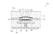
- Example 3-1 An ESD protection device 10d of Example 3-1 will be described with reference to FIG.
- FIG. 6 is a cross-sectional view of the main part of the ESD protection device 10d.
- the conductor portions 34 and 35 are connected to the external conductor portions 38 and 39 via the via conductors 36 and 37, as in the case of Example 1-1.
- the conductor portions 34 and 35 and the via conductors 32 and 33 connected to the discharge electrodes 14 and 15 in the embodiment 1-1 are not provided.
- the ESD protection device 10d is not electrically connected to the discharge electrodes 14 and 15 and the conductor portions 34 and 35, the via conductors 36 and 37, and the external conductor portions 38 and 39, the ESD protection device 10d can dissipate heat. The diffusion of components can be suppressed. Therefore, it is possible to suppress deterioration of discharge characteristics due to repeated discharge.
- Example 3-2 An ESD protection device 10e of Example 3-2 will be described with reference to FIG.
- FIG. 7 is a cross-sectional view of an essential part of the ESD protection device 10e cut along a position corresponding to the line XX in FIG.
- conductor portions 34e and 35e are arranged between ceramic layers of the ceramic multilayer substrate 12 on which the discharge electrodes 14 and 15 are arranged.
- the conductor portions 34e and 35e extend to the side surfaces 12s and 12t of the ceramic multilayer substrate 12, and are connected to the external conductor portions 38e and 39e formed on the side surfaces 12s and 12t of the ceramic multilayer substrate 12.
- the conductor portions 34e and 35e are formed in the stacking direction in which the ceramic layers of the ceramic multilayer substrate 12 are stacked (in the direction perpendicular to the paper surface in FIG. 7) and in the facing direction in which the facing portions 14a and 15a of the discharge electrodes 14 and 15 face each other (see FIG. 7).
- the opposing ends 14 a, 15 a of the discharge electrodes 14, 15 are covered with the opposite ends 14 s, 15 s and further discharged.
- the tip portions 14a and 15s of the facing portions 14a and 15a of the electrodes 14 and 15 are formed so as to cover the facing region 13s facing each other at the shortest distance.
- part of the heat generated during discharge is radiated from the conductor portions 34e and 35e to the outside of the ESD protection device 10e via the external conductor portions 38e and 39e.
- the temperature rise of 14a and 15a can be suppressed.
- the glass component diffusion at the time of baking can be suppressed by the conductor parts 34e and 35e. Therefore, it is possible to suppress deterioration of discharge characteristics due to repeated discharge.
- Example 4 An ESD protection device 10f of Example 4 will be described with reference to FIG.
- FIG. 8 is a cross-sectional view of the main part of the ESD protection device 10f.
- the ESD protection device 10f is disposed on both sides in the stacking direction of the cavity portion 13, that is, on both sides in the stacking direction with respect to the opposing portions 14a and 15a of the discharge electrodes 14 and 15, as in Example 1-1.
- the conductor parts 34 and 35 are provided.
- the external conductor portions 38 and 39 and the via conductors 32 and 33; 36 and 37 that are in the embodiment 1-1 (see FIG. 1) are not provided.
- the ESD protection device 10f a part of heat generated at the time of discharge is radiated from the opposing portions 14a, 15a of the discharge electrodes 14, 15 to the conductor portions 34, 35. Moreover, the conductor parts 34 and 35 can suppress glass component diffusion during firing. Therefore, it is possible to suppress deterioration of discharge characteristics due to repeated discharge.
- Example 5-1 An ESD protection device 10g of Example 5-1 will be described with reference to FIG.
- FIG. 9 is a sectional view of an essential part of the ESD protection device 10g.
- the ESD protection device 10g is similar to the fourth embodiment in that the cavity 13 is one side in the stacking direction of the cavity 13, that is, the cavity 13 in the stacking direction with respect to the opposing portions 14a and 15a of the discharge electrodes 14 and 15.
- a conductor portion 34 disposed on the opposite side is provided.
- the conductor part 35 which was in Example 4 (see FIG. 8) is not provided.
- the conductor portions 34 and 35 are connected to the facing portions 14a and 15a of the discharge electrodes 14 and 15, respectively. It is possible to dissipate heat more effectively by disposing the conductor portion 34 at a position closer to. Moreover, the conductor part 34 can suppress the glass component diffusion at the time of baking. Therefore, it is possible to suppress deterioration of discharge characteristics due to repeated discharge.
- Example 5-2 An ESD protection device 10h according to Example 5-2 will be described with reference to FIG.
- FIG. 10 is a cross-sectional view of the main part of the ESD protection device 10h.
- the ESD protection device 10 h includes the hollow portion 13 among the conductor portions 33, 34, the via conductors 36, 37, and the external conductor portions 38, 38 in the embodiment 3-1 (see FIG. 6).
- the conductor part 35, the via conductor 37, and the outer conductor part 39 arranged on the cavity part 13 side are not provided.
- the ESD protection device 10h can radiate heat from the conductor part 34 to the outside of the ESD protection device 10h via the external conductor part 38. Moreover, the conductor part 34 can suppress the glass component diffusion at the time of baking. Therefore, it is possible to suppress deterioration of discharge characteristics due to repeated discharge.
- the ceramic material used as the material of the ceramic layer of the ceramic multilayer substrate is a material having a composition centered on Ba, Al, and Si. Each material is prepared and mixed to have a predetermined composition, and calcined at 800-1000 ° C. The obtained calcined powder is pulverized with a zirconia ball mill for 12 hours to obtain a ceramic powder. To this ceramic powder, an organic solvent such as toluene and echinene is added and mixed. Further, a binder and a plasticizer are added and mixed to obtain a slurry. The slurry thus obtained is molded by a doctor blade method to obtain a ceramic green sheet having a thickness of 50 ⁇ m.
- the ceramic multilayer substrate In order for the ceramic multilayer substrate to contain a glass component, glass is added to the ceramic raw material powder in advance. You may use the ceramic raw material powder with which glass is produced
- an electrode paste for forming the discharge electrode is prepared.
- An electrode paste is obtained by adding a solvent to a binder resin composed of 80 wt% Cu powder having an average particle size of about 1.5 ⁇ m and ethyl cellulose, and stirring and mixing with a roll.
- the mixed paste for forming the discharge auxiliary part is prepared by mixing Cu powder having an average particle diameter of about 3 ⁇ m as a metal material and silicon carbide (SiC) having an average particle diameter of 1 ⁇ m as a semiconductor material at a predetermined ratio, and a binder resin and a solvent. It is obtained by adding and stirring with a roll and mixing.
- the binder resin and the solvent are 40 wt%, and the remaining 60 wt% is Cu powder and silicon carbide.
- the resin paste consists of a resin and a solvent.
- a resin that decomposes and disappears upon firing is used.
- PET polypropylene
- ethyl cellulose acrylic resin and the like.
- a seal layer forming paste for forming the seal layer is prepared by the same method as the electrode paste.
- a seal layer forming paste (alumina paste) is obtained by stirring and mixing a binder resin composed of 50 wt% Al 2 O 3 powder having an average particle diameter of about 1 ⁇ m, ethyl cellulose, and the like with a solvent and 50 w%.
- the solid component of the seal layer forming paste is not particularly limited as long as it has a higher sintering temperature than the ceramic material of the ceramic multilayer substrate.
- alumina, zirconia, magnesia, mullite, quartz or the like can be selected.
- the electrode paste is filled into the through hole by screen printing to form a portion that becomes a via conductor.
- the through hole may be formed using a mold.
- a seal layer forming paste is applied by screen printing on a ceramic green sheet that becomes a ceramic layer adjacent to the discharge electrode, thereby forming a portion that becomes a seal layer.
- the mixed paste is applied by screen printing so as to form a predetermined pattern on the ceramic green sheet that becomes one of the ceramic layers adjacent to the discharge electrode in order to form a discharge assisting portion.
- a concave portion provided in advance in the ceramic green sheet may be filled with the mixed paste of silicon carbide / Cu powder.
- electrode paste is applied by screen printing to form a discharge electrode having a facing portion.
- the discharge electrode was formed to have a thickness of 100 ⁇ m and a discharge gap width (a dimension of a distance between the opposed tips of the facing portions) of 30 ⁇ m.
- a resin paste is applied by screen printing in order to form a cavity on the top.
- an electrode paste is applied by screen printing on a ceramic green sheet that becomes one of the ceramic layers adjacent to the conductor part and the external conductor part, thereby forming the conductor part and the external conductor part. You may form a conductor part and an external conductor part using metal foil.
- the manufacturing process can be simplified, but other metals such as Al, Au, and Ni may be used. Use of Ag with high thermal conductivity is effective for heat dissipation.
- the conductor part and the outer conductor part are preferably thick and highly dense in order to improve heat dissipation and suppress glass diffusion.
- the denseness can be increased, and the thickness can be increased by increasing the solid content ratio of the conductive paste or by increasing the plate thickness of the printing pattern.
- the conductor part and the outer conductor part are formed of a metal foil, it is only necessary to increase the thickness of the metal foil.
- Firing Next firing is performed in an N 2 atmosphere in the same manner as a normal ceramic multilayer substrate.
- a rare gas such as Ar or Ne
- the temperature region in which the ceramic material is contracted and sintered may be fired in a rare gas atmosphere such as Ar and Ne.
- a rare gas atmosphere such as Ar and Ne.
- an electrode material such as Ag
- an air atmosphere may be used.
- the resin paste disappears and a cavity is formed. Moreover, the organic solvent in a ceramic green sheet, the binder resin in a mixed paste, and a solvent are also lose
- electrolytic Ni—Sn plating is performed on the external electrodes.
- the semiconductor material in the mixed paste is not particularly limited to the above materials.
- metal semiconductors such as silicon and germanium, carbides such as silicon carbide, titanium carbide, zirconium carbide, molybdenum carbide and tungsten carbide, nitrides such as titanium nitride, zirconium nitride, chromium nitride, vanadium nitride and tantalum nitride, titanium silicide , Silicides such as zirconium silicide, tungsten silicide, molybdenum silicide, chromium silicide, chromium silicide, titanium boride, zirconium boride, chromium boride, lanthanum boride, molybdenum boride, tungsten boride, etc.
- Oxides such as borides, zinc oxide, and strontium titanate can be used.
- silicon and silicon carbide are particularly preferable because they are relatively inexpensive and various particle size variations are commercially available.
- These semiconductor materials may be used alone or in admixture of two or more. Further, the semiconductor material may be used by appropriately mixing with a resistance material such as alumina or BAS material.
- the metal material in the mixed paste is not particularly limited to the above materials. Cu, Ag, Pd, Pt, Al, Ni, W, Mo, alloys thereof, or combinations thereof may be used.
- a resin paste is applied to form the hollow portion, but it is sufficient that the resin paste disappears even if it is not a resin, such as carbon. You may arrange
- the method of cutting before firing and dividing into chips was shown.
- the ceramic green sheets formed in an aggregated state are laminated and divided grooves are formed in the laminate formed by pressure bonding. After forming, firing, and plating, each chip may be cut.
- the ESD discharge response was evaluated for each sample.
- the ESD discharge responsiveness was measured by an electrostatic discharge immunity test defined in the IEC standard, IEC61000-4-2. 8 kV was applied by contact discharge, and the peak voltage during discharge was detected on the protection circuit side.
- ESD repeatability was evaluated.
- Application of 8 kV was performed 100 times by contact discharge, and then the discharge responsiveness to the ESD was evaluated.
- ESD voltage resistance is poor when the peak voltage detected on the protection circuit side is 700V or more (x mark), peak voltage is 600V or more and less than 700V is good (circle mark), and peak voltage is particularly good when the peak voltage is less than 600V ( ⁇ ).
- Table 1 below shows the evaluation results.
- the unit of the numerical value (peak voltage) in the “ESD discharge responsiveness” column and the “ESD repetition resistance” column is V.
- each example shows improvement in the initial ESD discharge response.
- a heat radiating conductor electrode
- the former having higher heat dissipation improves the ESD repeatability than the latter.
- Example 1-1 FIG. 1
- Example 3-1 FIG. 6
- Example 2-1 FIG. 4
- the heat-dissipating conductor is connected to the discharge electrode
- the heat-dissipating conductor is connected to the external conductor
- the heat-dissipating conductor is connected to the opposite side of the discharge electrode from both sides.
- the heat dissipating effect is enhanced by arranging the heat-dissipating conductor part so that it is covered not in the same layer as the opposite part of the discharge electrode but in the stacking direction. , ESD repeatability is improved.
- the body of the ESD protection device is not limited to a ceramic multilayer substrate, and may be an insulating multilayer substrate in which an insulating layer such as a resin is laminated.
- the conductor portion may be configured such that the width of the portion covering the facing portion of one discharge electrode is different from the width of the portion covering the facing portion of the other discharge electrode. For example, since heat is generated at the facing portion of the discharge electrode on the side receiving electrons during discharge, the width of the portion covering the facing portion of the discharge electrode on the side receiving electrons during discharging covers the facing portion of the other discharge electrode If the conductor portion is formed so as to be larger than the width of the substrate and heat dissipation is promoted, deterioration of the discharge characteristics can be suppressed more reliably.
- the conductor portions are collectively placed on the side where the number of ceramic layers of the ceramic multilayer substrate is relatively large with respect to the discharging electrode. Then, it is more effective.
- the cavity is preferably disposed on the side opposite to the conductor, that is, on the side where the number of ceramic layers of the ceramic multilayer substrate is relatively small with respect to the portion facing the discharge electrode.
- Discharge auxiliary part 12 Ceramic multilayer substrate 12a Upper surface 12b Lower surface 12p, 12q End surface (surface) 12s, 12t Side surface 13 Cavity portion 13s Opposing region 14 Discharge electrode 14a Opposing portion 14s Tip 15 Discharge electrode 15a Opposing portion 15s Tip 15 Conductor portion 16, 17 Seal layer 18, 19 External electrode 32, 32a Via conductor 33, 33a Via conductor 33 , 34 Conductor part 34 Conductor part 34, 35 Conductor part 34a, 35a Conductor part 34e, 35e Conductor part 35 Conductor part 36 Via conductor 36, 36a Via conductor 37, 37a Via conductor 38, 38a, 38e External conductor part 39, 39a, 39e outer conductor
Abstract
放電の繰り返しによる放電特性の劣化と、ガラス成分の拡散による過焼結とを抑制することができるESD保護デバイスを提供する。 複数の絶縁層が積層された絶縁性多層基板12の内部に、空洞部13と、少なくとも一対の放電電極14,15と、導体部34,35とが形成される。放電電極14,15は、空洞部13の内面に沿って形成され間隔を設けて互いに対向する対向部14a,15aを有し、外部電極18,19と接続されている。導体部34,35は、絶縁性多層基板12の絶縁層が積層された積層方向、放電電極14,15の対向部14a,15aが互いに対向する対向方向、又は積層方向と対向方向との両方に対して垂直な方向に透視したときに放電電極14,15の対向部14a,15aの互いに対向する先端14s,15sの少なくとも一方を覆うように、形成される。
Description
本発明は、ESD保護デバイスに関し、詳しくは、セラミック多層基板の内部に形成された空洞部内に露出する放電電極の対向部間で放電が発生するESD保護デバイスに関する。
ESD(Electro-Static Discharge;静電気放電)とは、帯電した導電性の物体(人体等)が、他の導電性の物体(電子機器等)に接触、あるいは充分接近したときに、激しい放電が発生する現象である。ESDにより電子機器の損傷や誤作動などの問題が発生する。これを防ぐためには、放電時に発生する過大な電圧が電子機器の回路に加わらないようにする必要がある。このような用途に使用されるのがESD保護デバイスであり、サージ吸収素子やサージアブソーバとも呼ばれている。
ESD保護デバイスは、例えば回路の信号線路とグランド(接地)との間に配置する。ESD保護デバイスは、一対の放電電極を離間して対向させた構造であるので、通常の使用状態では高い抵抗を持っており、信号がグランド側に流れることはない。これに対し、例えば携帯電話等のアンテナから静電気が加わる場合のように、過大な電圧が加わると、ESD保護デバイスの放電電極間で放電が発生し、静電気をグランド側に導くことができる。これにより、ESDデバイスよりも後段の回路には、静電気による電圧が印加されず、回路を保護することができる。
例えば図12の断面図に示すESD保護デバイス1は、セラミック多層基板2の内部に空洞部3と、間隔5を設けて対向する放電電極6,8とが形成されている。放電電極6,8は、空洞部3の内面に沿って形成された対向部7,9を含む。放電電極6,8は、空洞部3からセラミック多層基板2の外周面まで延在し、セラミック多層基板2の外側、すなわちセラミック多層基板2の表面に形成された外部電極6x,8xに接続されている。外部電極6x,8xは、ESD保護デバイス1を実装するために用いる。放電電極6,8の対向部7,9と対向部7,9間の間隔5が形成された部分とに隣接して、導電材料が分散している補助電極4が形成されている。
外部電極6x,8xに所定値以上の電圧が印加されると、放電電極6,8の対向部7,9間において放電が発生し、その放電により過剰な電圧をグランドへ導き、後段の回路を保護することができる。放電電極6,8の対向部7,9間の間隔5や、補助電極4に含まれる導電材料の量や種類などを調整することにより放電開始電圧を設定することができる(例えば、特許文献1参照)。
ESD保護デバイスは、放電を繰り返すと、放電時の熱や衝撃によって放電電極の対向部が溶けたり剥がれたりして、放電電極の対向部間のギャップが大きくなり、その結果、放電開始電圧が高くなり、放電特性が劣化することがある。
特に、放電電極が導電性ペーストの印刷により形成された場合には、図11(a)の要部断面図に示すように、空洞部13の内面に沿って形成される放電電極14,15の対向部14a,15aの端部は、薄く形成されることが多い。放電を繰り返すと、図11(b)の要部断面図に示すように、電子を受ける側の放電電極14の対向部14aが剥がれたり、溶けて短くなったりして、放電電極14,15の対向部14a,15a間のギャップが大きくなりやすいため、放電特性の劣化は、より深刻な問題となる。
また、ESD保護デバイスの本体であるセラミック多層基板を構成するセラミックがガラス成分を含む場合、ESD保護デバイスの焼成時にガラス成分が、放電電極の対向部の薄く形成された先端部に拡散すると焼結が過剰に進行して、微細な金属粒子が緻密に分散した理想状態ではなく、金属粒子が大きく成長し、金属粒子の間に大きな空隙が形成された過焼結状態となる。過焼結状態の放電電極の対向部は、放電時の熱によって金属粒子がさらに大きく成長し、金属粒子が玉状に孤立した、いわゆる玉化状態となり、放電ギャップが実質的に大きくなるため、放電特性が劣化しやすい。補助電極についても、ガラス成分によって過焼結状態となると、放電時の熱によって導電材料の粒子が成長して導電材料の粒子間の距離が拡大し、放電を促進する効果が低減することにより、放電特性が劣化しやすい。
本発明は、かかる実情に鑑み、放電の繰り返しによる放電特性の劣化を抑制することができるESD保護デバイスを提供しようとするものである。
本発明は、上記課題を解決するために、以下のように構成したESD保護デバイスを提供する。
ESD保護デバイスは、a)複数の絶縁層が積層された絶縁性多層基板と、(b)前記絶縁性多層基板の内部に形成された空洞部と、(c)前記空洞部の内面に沿って形成され間隔を設けて互いに対向する対向部を有する、少なくとも一対の放電電極と、(d)前記絶縁性多層基板の表面に形成され、前記放電電極と接続された外部電極と、(e)前記絶縁性多層基板の前記絶縁層が積層された積層方向、前記放電電極の前記対向部が互いに対向する対向方向、又は前記積層方向と前記対向方向との両方に対して垂直な方向に透視したときに前記放電電極の前記対向部の互いに対向する先端の少なくとも一方を覆うように、前記セラミック多層基板の内部に形成された導体部とを備える。
上記構成において、外部電極間に所定以上の大きさの電圧が印加されると、放電電極の互いに対向する対向部間で放電が発生し、熱が発生する。放電時に発生する熱は、電気及び熱をよく通す導体部に逃がすことができる。
上記構成によれば、放電を繰り返しても放電電極の対向部の温度上昇が抑制される。そのため、放電時に発生する熱で放電電極の対向部が溶解したり剥がれたりすることによって放電電極の対向部間のギャップが大きくなって放電特性が劣化するのを抑制することができる。
好ましくは、前記導体部は、前記積層方向に透視したときに前記放電電極の前記対向部の互いに対向する前記先端の少なくとも一方を覆うように形成される。前記導体部と前記放電電極の前記対向部との間に、少なくとも1層の前記絶縁性多層基板の前記絶縁層が配置される。
この場合、導体部は、放電電極の対向部の互いに対向する先端に沿って放電電極の対向部を広く覆い、放電電極の対向部の互いに対向する先端に対向する面積が大きく、放電時の熱を逃がす効果が高い。そのため、放電特性の劣化をより確実に抑制することができる。
好ましくは、前記絶縁性多層基板は、ガラス成分を含むセラミック多層基板である。
この場合、ESD保護デバイスの焼成時に、導体部に関して放電電極の対向部とは反対側にあるガラス成分は、導体部によって、放電電極の対向部に向かっての移動が阻止される。これにより、ガラス成分による放電電極の対向部の過焼結が抑制されるので、放電電極の対向部の過焼結に起因する放電特性劣化を抑制することができる。
好ましくは、前記放電電極の前記対向部の前記先端同士が最短距離で対向する対向領域に形成され、分散した金属材料と半導体材料とを含む放電補助部をさらに備える。前記導体部は、前記積層方向に透視したときに前記対向領域を覆うように形成される。
対向領域に、放電補助部の金属材料と半導体材料とが分散した状態で配置されていると、電子の移動が起こりやすくなるため、効率的に放電現象が生じ、放電特性が安定する。導体部は、放電時に対向領域で発生する熱を効果的に放熱することができる。絶縁性多層基板がガラス成分を含むセラミック多層基板である場合には、ESD保護デバイスの焼成時に、導体部に関して放電補助部とは反対側にあるガラス成分は、導体部によって、放電補助部に向かっての移動が阻止される。これにより、ガラス成分による放電補助部の過焼結が抑制されるので、放電補助部の過焼結に起因する放電特性劣化を抑制することができる。
好ましくは、前記導体部は、前記放電電極の前記対向部に関して前記積層方向かつ前記空洞部とは反対側に配置される。
この場合、導体部と放電電極の対向部との間に空洞部が介在しないので、導体部を放電電極の対向部により近い位置に配置して、より効果的に放熱を行うことができる。また、絶縁性多層基板がガラス成分を含むセラミック多層基板である場合に、ESD保護デバイスの焼成時に、ガラス成分の拡散をより効果的に抑制することができる。
好ましくは、前記導体部は、前記絶縁性多層基板の異なる前記絶縁層間の複数個所に配置される。
この場合、複数個所に導体部を設けることによって、放熱とガラス成分の拡散抑制とをより確実に行うことができる。
好ましくは、前記導体部は、前記放電電極の前記対向部に関して前記積層方向両側に配置される。
この場合、放電電極の対向部の両主面側に導体部を配置することにより、放熱とガラス成分の拡散抑制とをより確実に行うことができる。
好ましくは、前記導体部は、前記放電電極と電気的に接続される。
この場合、導体部と放電電極との間は電気及び熱をよく通すため、導体部から放電電極及び外部電極を経てESD保護デバイスの外部に放熱することができるので、放熱をより確実に行うことができる。
好ましくは、(f)前記絶縁性多層基板の表面に形成された外部導体部をさらに備える。前記導体部と前記外部導体部とが電気的に接続される。
この場合、外部導体部は電気及び熱をよく通し、導体部と外部導体部との間は電気及び熱をよく通すため、導体部から外部導体部を経てESD保護デバイスの外部に放熱することができるので、放熱をより確実に行うことができる。
好ましくは、(g)前記放電電極の前記対向部と前記絶縁層基板の前記絶縁層との間に配置され、前記絶縁層基板の前記絶縁層に含まれる成分の透過を抑制するシール層をさらに備える。
この場合、絶縁性多層基板に含まれる成分は、シール層の透過抑制によって、放電電極の対向部に達しにくくなるため、放電電極の対向部が絶縁性多層基板に含まれる成分の影響を受けて放電特性の劣化をもたらすのを抑制することができる。絶縁性多層基板がガラス成分を含むセラミック多層基板である場合には、ガラス成分の拡散による放電電極の対向部や放電補助部の過焼結に起因する放電特性の劣化を抑制することができる。
本発明によれば、放電の繰り返しによる放電特性の劣化を抑制することができる。
以下、本発明の実施の形態について、図1~図10を参照しながら説明する。
<実施例1-1> 実施例1-1のESD保護デバイス10について、図1及び図2を参照しながら説明する。
図1は、ESD保護デバイス10の断面図である。図2は、図1の線X-Xに沿って切断した要部断面図である。
図1及び図2に示すように、ESD保護デバイス10は、図1において上下方向に複数のセラミック層が積層されたセラミック多層基板12の内部に形成された空洞部13と一対の放電電極14,15とを備えている。放電電極14,15は、空洞部13の内面に沿って形成され間隔を設けて互いに対向し空洞部13内に露出する対向部14a,15aを有する。セラミック多層基板12の端面12p,12qには外部電極18,19が形成され、外部電極18,19は放電電極14,15と接続されている。外部電極18,19は、ESD保護デバイス10を回路基板等に実装するために用いられる。
さらに、セラミック多層基板12の内部には、セラミック多層基板12のセラミック層間に配置された導体部34,35と、セラミック多層基板12のセラミック層を貫通するビア導体32,33;36,37とが形成されている。導体部34,35は、ビア導体32,33を介して、放電電極14,15に接続されている。導体部34,35とビア導体32,33と放電電極14,15とは、電気と熱をよく通す導体であり、導体部34,35は放電電極14,15と電気的に接続されている。
導体部34,35は、セラミック多層基板12のセラミック層が積層される積層方向(図1において上下方向)から透視すると、図2に示すように、放電電極14,15の対向部14a,15aの互いに対向する先端14s,15sを覆い、さらに放電電極14,15の対向部14a,15aの先端14s,15s同士が最短距離で対向する対向領域13sを覆うように形成されている。
セラミック多層基板12の上面12a及び下面12bには、外部導体部38,39が形成されている。外部導体部38,39は、ビア導体36,37を介して、導体部34,35に接続されている。導体部34,35とビア導体36,37と外部導体38,39とは、電気と熱をよく通す導体であり、導体部34,35は外部導体38,39と電気的に接続されている。
セラミック多層基板12と空洞部13との間には、シール層16,17が形成されている。シール層16,17は、例えば、セラミック多層基板12を構成しているセラミックスよりも焼結温度が高いセラミックスからなる。シール層16,17を設けることにより、焼成時に、セラミック多層基板12のセラミック中に含まれるガラス成分の拡散を阻止し、放電電極14,15の対向部14a,15aの過焼結を抑制することができる。なお、シール層16,17を設けない構成とすることも可能である。
一方のシール層16の上には、図1において●と○で模式的に示すように、放電電極14,15の対向部14a,15aの先端14s,15s同士が最短距離で対向する対向領域13sに、放電補助部11が形成されている。放電補助部11は、分散した金属材料と半導体材料とを含む。放電時に電子が移動する対向領域13sに、放電補助部11の金属材料と半導体材料とが分散した状態で配置されていると、電子の移動が起こりやすくなるため、効率的に放電現象が生じ、放電特性が安定する。
なお、放電補助部11は、対向領域13sに隣接する領域にも形成しても構わない。例えば、放電電極14,15の対向部14a,15aの上や、放電電極14,15の対向部14a,15aとシール層16との間などにも、形成しても構わない。
ESD保護デバイス10は、外部電極18,19間に所定以上の大きさの電圧が印加されると、空洞部13内において、すなわち、放電電極14,15の対向部14a,15a間で、放電が発生する。放電時に発生する熱は、導体部34,35からビア導体36,37、外部導体部38,39を経てESD保護デバイス10の外部に放熱されたり、導体部34,35からビア導体32,33、放電電極14,15、外部電極18,19を経てESD保護デバイス10の外部に放熱されたりする。このような放熱によって、放電電極14,15の対向部14a,15aの温度上昇を抑制することができる。そのため、放電の繰り返しによって放電電極14,15の対向部14a,15aが溶解したり剥がれたりすることによって放電電極14,15の対向部14a,15a間のギャップが大きくなって、あるいは玉化して放電電極14,15の対向部14a,15a間のギャップが実質的に大きくなって放電特性が劣化するのを抑制することができる。
また、ESD保護デバイス10の焼成時に、導体部34,35に関して放電電極14,15の対向部14a,15aとは反対側にあるガラス成分は、導体部34,35によって、放電電極14,15の対向部14a,15aや放電補助部11に向かっての移動が阻止される。これにより、ガラス成分による放電電極14,15の対向部14a,15aや放電補助部11の過焼結が抑制されるので、放電電極14,15の対向部14a,15aや放電補助部11の過焼結に起因する放電特性劣化を抑制することができる。
導体部34,35は、複数個所に、すなわち、放電電極14,15の対向部14a,15aに関してセラミック多層基板12のセラミック層の積層方向両側に配置されているので、放熱とガラス成分の拡散抑制とをより確実に行うことができる。
導体部34,35は、放電電極14,15の対向部14a,15aの互いに対向する先端14s,15sに沿って、放電電極14,15の対向部14a,15aを広く覆い、積層方向に透視したときに対向領域13sを覆うように形成されている。導体部34,35は、放電電極14,15の対向部14a,15aの互いに対向する先端14s,15sに対向する面積が大きく、放電時の熱を逃がす効果が高いため、放電特性の劣化をより確実に抑制することができる。
<実施例1-2> 実施例1-2のESD保護デバイス10aについて、図3を参照しながら説明する。
実施例1-2のESD保護デバイス10aは、実施例1-1のESD保護デバイス10と略同様に構成されている。以下では、実施例1-1と同じ構成部分には同じ符号を用い、実施例1-1との相違点を中心に説明する。
図3は、ESD保護デバイス10aの要部断面図である。図3に示すように、ESD保護デバイス10aは、実施例1-1と同様にセラミック多層基板12のセラミック層間に配置された導体部34a,35aと、外部導体部38a,39aと、ビア導体32a,33a;36a,37aとを備えるが、それらのいずれもが空洞部13の片側、すなわち、放電電極14,15の対向部14a,15aに関して積層方向に空洞部13とは反対側に配置されている。導体部34a,35aは、ビア導体32a,33aを介して放電電極14,15に接続され、また、ビア導体36a,37aを介して外部導体部38a,39aと接続されている。外部導体部38a,39aは互いに十分離れているため、外部導体部38a,39a間で放電は発生しない。
ESD保護デバイス10aは、導体部34a,35aと放電電極14,15の対向部14a,15aとの間に空洞部13が介在しないので、導体部34a,35aを放電電極14,15の対向部14a,15aにより近い位置に配置して、より効果的に放熱を行うことができる。また、ガラス成分の拡散をより効果的に抑制することができる。複数個所に導体部34a,35aが設けられているので、放熱とガラス成分の拡散抑制とをより確実に行うことができる。したがって、放電の繰り返しによる放電特性の劣化を抑制することができる。
<実施例2-1> 実施例2-1のESD保護デバイス10bについて、図4を参照しながら説明する。
図4は、ESD保護デバイス10bの要部断面図である。図4に示すように、ESD保護デバイス10aは、実施例1-1と同様に、セラミック多層基板12のセラミック層間に配置された導体部34,35は、放電電極14,15の対向部14a,15aに関して積層方向両側に配置され、ビア導体32,33を介して放電電極14,15に接続されている。しかし、実施例1-1(図1参照)にはあった外部導体部38,39及びビア導体36,37は備えていない。
ESD保護デバイス10cは、放電電極14,15の対向部14a,15aの両主面側に導体部34,35が配置され、導体部34,35が放電電極14,15に接続されているため、放熱とガラス成分の拡散抑制とをより確実に行うことができる。したがって、放電の繰り返しによる放電特性の劣化を抑制することができる。
<実施例2-2> 実施例2-2のESD保護デバイス10cについて、図5を参照しながら説明する。
図5は、ESD保護デバイス10cの要部断面図である。図5に示すように、ESD保護デバイス10cは、実施例1-2と同様に、空洞部13の片側、すなわち、放電電極14,15の対向部14a,15aに関して積層方向に空洞部13とは反対側に配置されている導体部34a,35aとビア導体32a,33aとを備えている。しかし、実施例1-2(図3参照)にはあった外部導体部38a,39aと外部導体部38a,39aに接続されたビア導体36a,37aとは、備えていない。
ESD保護デバイス10cは、導体部34a,35aと放電電極14,15の対向部14a,15aとの間に空洞部13が介在しないので、導体部34a,35aを放電電極14,15の対向部14a,15aにより近い位置に配置して、より効果的に放熱を行うことができる。また、ガラス成分の拡散をより効果的に抑制することができる。
また、複数個所に導体部34a,35aが設けられているので、放熱やガラス成分の拡散抑制をより確実に行うことができる。したがって、放電の繰り返しによる放電特性の劣化を抑制することができる。
<実施例3-1> 実施例3-1のESD保護デバイス10dについて、図6を参照しながら説明する。
図6は、ESD保護デバイス10dの要部断面図である。図6に示すように、ESD保護デバイス10dは、実施例1-1と同様に、導体部34,35がビア導体36,37を介して外部導体部38,39に接続されている。しかし、実施例1-1(図1参照)にはあった導体部34,35と放電電極14,15と接続されたビア導体32,33は、備えていない。
ESD保護デバイス10dは、放電電極14,15と、導体部34,35、ビア導体36,37及び外部導体部38,39とは電気的に接続されていないが、放熱を行うことができ、ガラス成分の拡散を抑制することができる。したがって、放電の繰り返しによる放電特性の劣化を抑制することができる。
<実施例3-2> 実施例3-2のESD保護デバイス10eについて、図7を参照しながら説明する。
図7は、図1の線X-Xに該当する位置に沿って切断したESD保護デバイス10eの要部断面図である。図7に示すように、ESD保護デバイス10eは、放電電極14,15が配置されるセラミック多層基板12のセラミック層間に、導体部34e,35eが配置されている。導体部34e,35eは、セラミック多層基板12の側面12s,12tまで延在し、セラミック多層基板12の側面12s,12tに形成された外部導体部38e,39eと接続されている。
導体部34e,35eは、セラミック多層基板12のセラミック層が積層された積層方向(図7において紙面垂直方向)と、放電電極14,15の対向部14a,15aが互いに対向する対向方向(図7において左右方向)との両方に対して垂直な方向(図7において上下方向)に透視したときに、放電電極14,15の対向部14a,15aの互いに対向する先端14s,15sを覆い、さらに放電電極14,15の対向部14a,15aの先端14s,15s同士が最短距離で対向する対向領域13sを覆うように形成されている。
ESD保護デバイス10eは、放電時に発生する熱の一部が、導体部34e,35eから外部導体部38e,39eを経てESD保護デバイス10eの外部に放熱されるので、放電電極14,15の対向部14a,15aの温度上昇を抑制することができる。また、導体部34e,35eによって、焼成時のガラス成分拡散を抑制することができる。したがって、放電の繰り返しによる放電特性の劣化を抑制することができる。
<実施例4> 実施例4のESD保護デバイス10fについて、図8を参照しながら説明する。
図8は、ESD保護デバイス10fの要部断面図である。図8に示すように、ESD保護デバイス10fは、実施例1-1と同様に、空洞部13の積層方向両側、すなわち、放電電極14,15の対向部14a,15aに関して積層方向両側に配置されている導体部34,35を備えている。しかし、実施例1-1(図1参照)にはあった外部導体部38,39とビア導体32,33;36,37とは、備えていない。
ESD保護デバイス10fは、放電時に発生した熱の一部が、放電電極14,15の対向部14a,15aから導体部34,35に放熱される。また、導体部34,35によって、焼成時のガラス成分拡散を抑制することができる。したがって、放電の繰り返しによる放電特性の劣化を抑制することができる。
<実施例5-1> 実施例5-1のESD保護デバイス10gについて、図9を参照しながら説明する。
図9は、ESD保護デバイス10gの要部断面図である。図9に示すように、ESD保護デバイス10gは、実施例4と同様に、空洞部13の積層方向片側、すなわち、放電電極14,15の対向部14a,15aに関して積層方向に空洞部13とは反対側に配置されている導体部34を備えている。しかし、実施例4(図8参照)にはあった導体部35は、備えていない。
ESD保護デバイス10gは、導体部34と放電電極14,15の対向部14a,15aとの間に空洞部13が介在しないので、導体部34,35を放電電極14,15の対向部14a,15aにより近い位置に導体部34を配置して、より効果的に放熱を行うことができる。また、導体部34は、焼成時のガラス成分拡散を抑制することができる。したがって、放電の繰り返しによる放電特性の劣化を抑制することができる。
<実施例5-2> 実施例5-2のESD保護デバイス10hについて、図10を参照しながら説明する。
図10は、ESD保護デバイス10hの要部断面図である。図10に示すように、ESD保護デバイス10hは、実施例3-1(図6参照)にあった導体部33,34とビア導体36,37と外部導体部38,38のうち、空洞部13の積層方向片側、すなわち、放電電極14,15の対向部14a,15aに関して積層方向に空洞部13とは反対側に配置されている導体部34、ビア導体36及び外部導体部38を備えているが、空洞部13側に配置されている導体部35、ビア導体37及び外部導体部39は備えていない。
ESD保護デバイス10hは、導体部34から外部導体部38を経てESD保護デバイス10hの外部に放熱を行うことができる。また、導体部34は、焼成時のガラス成分拡散を抑制することができる。したがって、放電の繰り返しによる放電特性の劣化を抑制することができる。
<作製例> 上記各実施例のESD保護デバイスの作製例について、説明する。
(1)材料の準備
セラミック多層基板のセラミック層の材料となるセラミック材料には、Ba、Al、Siを中心とした組成からなる材料を用いる。各素材を所定の組成になるよう調合、混合し、800-1000℃で仮焼する。得られた仮焼粉末をジルコニアボールミルで12時間粉砕し、セラミック粉末を得る。このセラミック粉末に、トルエン・エキネンなどの有機溶媒を加え混合する。さらにバインダー、可塑剤を加え混合し、スラリーを得る。このようにして得られたスラリーをドクターブレード法により成形し、厚さ50μmのセラミックグリーンシートを得る。
セラミック多層基板のセラミック層の材料となるセラミック材料には、Ba、Al、Siを中心とした組成からなる材料を用いる。各素材を所定の組成になるよう調合、混合し、800-1000℃で仮焼する。得られた仮焼粉末をジルコニアボールミルで12時間粉砕し、セラミック粉末を得る。このセラミック粉末に、トルエン・エキネンなどの有機溶媒を加え混合する。さらにバインダー、可塑剤を加え混合し、スラリーを得る。このようにして得られたスラリーをドクターブレード法により成形し、厚さ50μmのセラミックグリーンシートを得る。
セラミック多層基板がガラス成分を含むようにするため、セラミック原料粉末に予めガラスを添加する。焼成時にガラスが生成されるセラミック原料粉末を用いてもよい。
また、放電電極を形成するための電極ペーストを作製する。平均粒径約1.5μmのCu粉80wt%とエチルセルロース等からなるバインダー樹脂に溶剤を添加し、ロールで攪拌、混合することで電極ペーストを得る。
放電補助部を形成するための混合ペーストは、金属材料として平均粒径約3μmのCu粉と、半導体材料として平均粒径1μmの炭化ケイ素(SiC)を所定の割合で調合し、バインダー樹脂と溶剤を添加し、ロールで攪拌、混合することで得る。混合ペーストは、バインダー樹脂と溶剤を40wt%とし、残りの60wt%をCu粉と炭化ケイ素とする。
また、空洞部を形成するための樹脂ペーストも同様の方法にて作製する。樹脂ペーストは、樹脂と溶剤からなる。樹脂材料には焼成時に分解、消失する樹脂を用いる。例えばPET、ポリプロピレン、エチルセルロース、アクリル樹脂などである。
また、シール層を形成するためのシール層形成用ペーストを、電極ペーストと同様の手法で作製する。例えば、平均粒径約1μmのAl2O3粉50wt%とエチルセルロース等からなるバインダー樹脂と溶剤50w%をロールで攪拌、混合することで、シール層形成用ペースト(アルミナペースト)を得る。シール層形成用ペーストの固形成分には、セラミック多層基板のセラミック材料よりも焼結温度が高い材料であれば特に限定されない。例えば、アルミナ、ジルコニア、マグネシア、ムライト、石英などを選定することができる。
(2)スクリーン印刷によるペーストの塗布
セラミックグリーンシートに、レーザを用いて貫通孔を形成した後、スクリーン印刷により、貫通孔に電極ペーストを充填して、ビア導体になる部分を形成する。貫通孔は、金型を用いて形成しても構わない。
セラミックグリーンシートに、レーザを用いて貫通孔を形成した後、スクリーン印刷により、貫通孔に電極ペーストを充填して、ビア導体になる部分を形成する。貫通孔は、金型を用いて形成しても構わない。
次いで、放電電極に隣接するセラミック層になるセラミックグリーンシートの上に、シール層形成用ペーストをスクリーン印刷にて塗布して、シール層になる部分を形成する。
次いで、放電電極に隣接する一方のセラミック層になるセラミックグリーンシートの上に、放電補助部を形成するため、混合ペーストを所定のパターンになるよう、スクリーン印刷にて塗布する。混合ペーストの厚みが大きい場合などには、セラミックグリーンシートに予め設けた凹部に、炭化ケイ素/Cu粉の混合ペーストを充填するようにしても構わない。
その上に、電極ペーストをスクリーン印刷にて塗布して、対向部を有する放電電極を形成する。作製例では、放電電極の太さを100μm、放電ギャップ幅(対向部の互いに対向する先端間の間隔の寸法)を30μmとなるように形成した。
さらにその上に、空洞部を形成するため、樹脂ペーストをスクリーン印刷にて塗布する。
また、導体部や外部導体部に隣接する一方のセラミック層になるセラミックグリーンシートの上に、電極ペーストをスクリーン印刷にて塗布して、導体部や外部導体部を形成する。金属箔を用いて、導体部や外部導体部を形成してもよい。
電極ペーストを用いて導体部や外部導体部を形成すると製造工程を簡略化できるが、AlやAu、Niなど他の金属を用いてもよい。放熱のためには熱伝導度が大きいAgを用いると効果が高い。
導体部や外部導体部は、放熱性向上とガラス拡散抑制のためには、厚みが厚く、緻密性が高いものが好ましい。導体部や外部導体部を導電性ペーストで形成する場合は、導電性ペーストに含まれる金属粉末の球形度を上げたり、粒度分布を広くしたり、樹脂比率を下げることにより金属粉末の充填性を上げると緻密性を高くすることができ、導電性ペーストの固形分比率を上げたり、印刷パターンの版厚を厚くすることにより、厚みをより厚くすることができる。導体部や外部導体部を金属箔で形成する場合は、金属箔の厚みを厚くするだけでよい。
(3)積層、圧着
通常のセラミック多層基板と同様に、セラミックグリーンシートを積層し、圧着する。作製例では、厚み0.3mm、その中央に放電電極の対向部と空洞部とが配置されるように積層した。
通常のセラミック多層基板と同様に、セラミックグリーンシートを積層し、圧着する。作製例では、厚み0.3mm、その中央に放電電極の対向部と空洞部とが配置されるように積層した。
(4)カット、端面電極塗布
LCフィルタのようなチップタイプの電子部品と同様に、マイクロカッタでカットして、各チップにわける。作製例では、1.0mm×0.5mmになるようにカットした。その後、端面に電極ペーストを塗布し、外部電極を形成する。
LCフィルタのようなチップタイプの電子部品と同様に、マイクロカッタでカットして、各チップにわける。作製例では、1.0mm×0.5mmになるようにカットした。その後、端面に電極ペーストを塗布し、外部電極を形成する。
(5)焼成
次いで、通常のセラミック多層基板と同様に、N2雰囲気中で焼成する。ESDに対する応答電圧を下げるため空洞部にAr、Neなどの希ガスを導入する場合には、セラミック材料の収縮、焼結が行われる温度領域をAr、Neなどの希ガス雰囲気で焼成すればよい。酸化しない電極材料(Agなど)の場合には、大気雰囲気でも構わない。
次いで、通常のセラミック多層基板と同様に、N2雰囲気中で焼成する。ESDに対する応答電圧を下げるため空洞部にAr、Neなどの希ガスを導入する場合には、セラミック材料の収縮、焼結が行われる温度領域をAr、Neなどの希ガス雰囲気で焼成すればよい。酸化しない電極材料(Agなど)の場合には、大気雰囲気でも構わない。
焼成により、樹脂ペーストが消失し、空洞部が形成される。また、焼成により、セラミックグリーンシート中の有機溶剤や、混合ペースト中のバインダー樹脂及び溶剤も消失する。
(6)めっき
LCフィルタのようなチップタイプの電子部品と同様に、外部電極上に電解Ni-Snメッキを行う。
LCフィルタのようなチップタイプの電子部品と同様に、外部電極上に電解Ni-Snメッキを行う。
以上により、ESD保護デバイスが完成する。
なお、混合ペースト中の半導体材料は、特に上記の材料に限定されるものではない。例えば、シリコン、ゲルマニウム等の金属半導体、炭化ケイ素、炭化チタン、炭化ジルコニウム、炭化モリブデン、炭化タングステン等の炭化物、窒化チタン、窒化ジルコニウム、窒化クロム、窒化バナジウム、窒化タンタル等の窒化物、ケイ化チタン、ケイ化ジルコニウム、ケイ化タングステン、ケイ化モリブデン、ケイ化クロム、ケイ化クロム等のケイ化物、ホウ化チタン、ホウ化ジルコニウム、ホウ化クロム、ホウ化ランタン、ホウ化モリブデン、ホウ化タングステン等のホウ化物、酸化亜鉛、チタン酸ストロンチウム等の酸化物を用いることができる。特に、比較的安価で、かつ、各種粒径のバリエーションが市販されていることから、シリコンや炭化ケイ素が特に好ましい。これらの半導体材料は、適宜、単独又は2種類以上を混合して使用してもよい。また、半導体材料は、適宜、アルミナやBAS材等の抵抗材料と混合して使用してもよい。
混合ペースト中の金属材料は、特に上記の材料に限定されるものではない。Cu、Ag、Pd、Pt、Al、Ni、W、Moや、これらの合金、これらの組合せでもよい。
また、空洞部を形成するために樹脂ペーストを塗布したが、樹脂でなくともカーボンなど焼成で消失するものならばよいし、また、ペースト化して印刷で形成しなくとも、樹脂フィルムなどを所定の位置にのみ貼り付けるようにして配置してもよい。
また、本作製例においては、焼成前にカットを行い、各チップに分ける方法を示したが、集合状態で形成されたセラミックグリーンシートを積層し、圧着して形成された積層体に分割溝を形成し、焼成、めっき後に各チップにカットしてもよい。
上述した工程で作製した各実施例の作製例について、評価を行った。比較例として、導体部、外部導体部及びビア導体を備えていないESD保護デバイスを作製した。
各試料について、ESD放電応答性を評価した。ESD放電応答性は、IECの規格、IEC61000-4-2に定められている静電気放電イミュニティ試験によって行った。接触放電にて8kV印加して、保護回路側で放電時のピーク電圧を検出した。
さらに、ESD繰返し耐性を評価した。接触放電にて8kV印加を100回行い、続いて、前記のESDに対する放電応答性を評価した。
総合判定は、ESD繰返し耐性について、保護回路側で検出されたピーク電圧が700V以上を不良(×印)、ピーク電圧が600V以上700V未満を良好(○印)、ピーク電圧が600V未満を特に良好(◎印)と判定した。
次の表1に、評価結果を示す。

なお、「ESD放電応答性」欄及び「ESD繰返し耐性」欄の数値(ピーク電圧)の単位は、Vである。
表1から、各実施例は、当初のESD放電応答性にても改善がみれる。この理由として、放電電極部の対向部の周囲に、放熱用の導体部(電極)が配置されることにより、セラミック中からのガラス拡散が放電電極の対向部に進むことが阻害される。これにより放電電極の初期的な焼結が抑制されたのと同じ効果となり、放電電極の対向部の先端の玉化が抑制されるために、初期の放電電極の対向部間のギャップが安定するためと考えられる。
表1から、ESD繰返し耐性は、放熱性が高いと向上することが分かる。
例えば、導体部が放電電極と電気的に接続された場合と導体部が放電電極と電気的に接続されていない場合とでは、放熱性が高い前者は、後者よりもESD繰返し耐性が向上する。これは、実施例1-1(図1)と実施例3-1(図6)との比較や、実施例2-1(図4)と実施例4(8)との比較から見て取ることができる。
導体部が外部導体に電気的に接続されている場合と、導体部が外部導体に電気的に接続されていない場合とでは、放熱性が高い前者は、後者よりもESD繰返し耐性が向上する。これは、実施例1-1(図1)と実施例2-1(図4)との比較や、実施例1-2(図3)と実施例2-2(図5)との比較から見て取ることができる。
導体部が放電電極の対向部に関して積層方向両側に配置されている場合と、導体部が放電電極の対向部に関して積層方向に空洞部とは反対側のみに配置されている場合とでは、放熱性が高い前者は、後者よりもESD繰返し耐性が向上する。これは、実施例3-1(図6)と実施例5-2(図10)との比較や、実施例4(図8)と実施例5-1(図9)との比較から見て取ることができる。
導体部が放電電極と異なるセラミック層間に配置される場合と、導体部が放電電極と同じセラミック層間に配置される場合とでは、前者は、後者よりもESD繰返し耐性が向上する。これは、実施例3-2と他の実施例との比較から見て取ることができる。
つまり『放電電極に放熱用の導体部が接続されている』、『放熱用の導体部が外部導体部に接続されている』、『放熱用の導体部が、放電電極の対向部を両側から挟むように配置する』、『放熱用の導体部が、放電電極の対向部と同じ層間で横に配置されるのではなく、積層方向に覆うように配置される』ことで放熱効果を高くなり、ESD繰返し耐性が向上する。
<まとめ> 以上に説明したように、放電電極に対向部に対向する導体部を設けることによって、放電の繰り返しによる放電特性の劣化を抑制することができる。
なお、本発明は、上記実施の形態に限定されるものではなく、種々変更を加えて実施することが可能である。
例えば、ESD保護デバイスの本体は、セラミック多層基板に限るものではなく、樹脂などの絶縁層が積層された絶縁性多層基板であればよい。
導体部は、一方の放電電極の対向部を覆う部分の幅と、他方の放電電極の対向部を覆う部分の幅とが異なるようにしてもよい。例えば、放電時に電子を受け取る側の放電電極の対向部で熱が発するため、放電時に電子を受け取る側の放電電極の対向部を覆う部分の幅の方が他方の放電電極の対向部を覆う部分の幅より大きくなるように導体部を形成して放熱を促進すると、より確実に放電特性の劣化を抑制することができる。
放電電極に対向部及び空洞部が積層方向片側に偏って配置される場合には、放電電極に対向部に関してセラミック多層基板のセラミック層の層数が相対的に多い側に導体部をまとめて配置すると、より効果がある。この場合、空洞部は、導体部とは反対側、すなわち放電電極に対向部に関してセラミック多層基板のセラミック層の層数が相対的に少ない側に配置することが好ましい。
10,10a~10h 保護デバイス
11 放電補助部
12 セラミック多層基板
12a 上面
12b 下面
12p,12q 端面(表面)
12s,12t 側面
13 空洞部
13s 対向領域
14 放電電極
14a 対向部
14s 先端
15 放電電極
15a 対向部
15s 先端
15 導体部
16,17 シール層
18,19 外部電極
32,32a ビア導体
33,33a ビア導体
33,34 導体部
34 導体部
34,35 導体部
34a,35a 導体部
34e,35e 導体部
35 導体部
36 ビア導体
36,36a ビア導体
37,37a ビア導体
38,38a,38e 外部導体部
39,39a,39e 外部導体部
Claims (10)
- 複数の絶縁層が積層された絶縁性多層基板と、
前記絶縁性多層基板の内部に形成された空洞部と、
前記空洞部の内面に沿って形成され間隔を設けて互いに対向する対向部を有する、少なくとも一対の放電電極と、
前記絶縁性多層基板の表面に形成され、前記放電電極と接続された外部電極と、
前記絶縁性多層基板の前記絶縁層が積層された積層方向、前記放電電極の前記対向部が互いに対向する対向方向、又は前記積層方向と前記対向方向との両方に対して垂直な方向に透視したときに前記放電電極の前記対向部の互いに対向する先端の少なくとも一方を覆うように、前記セラミック多層基板の内部に形成された導体部と、
を備えたことを特徴とする、ESD保護デバイス。 - 前記導体部は、前記積層方向に透視したときに前記放電電極の前記対向部の互いに対向する前記先端の少なくとも一方を覆うように形成され、
前記導体部と前記放電電極の前記対向部との間に、少なくとも1層の前記絶縁性多層基板の前記絶縁層が配置されることを特徴とする、請求項1に記載のESD保護デバイス。 - 前記絶縁性多層基板は、ガラス成分を含むセラミック多層基板であることを特徴とする、請求項1又は2に記載のESD保護デバイス。
- 前記放電電極の前記対向部の前記先端同士が最短距離で対向する対向領域に形成され、分散した金属材料と半導体材料とを含む放電補助部をさらに備え、
前記導体部は、前記積層方向に透視したときに前記対向領域を覆うように形成されたことを特徴とする、請求項1乃至3のいずれか一つに記載のESD保護デバイス。 - 前記導体部は、
前記放電電極の前記対向部に関して前記積層方向かつ前記空洞部とは反対側に配置されることを特徴とする、請求項1乃至4のいずれか一つに記載のESD保護デバイス。 - 前記導体部は、前記絶縁性多層基板の異なる前記絶縁層間の複数個所に配置されることを特徴とする、請求項1乃至5のいずれか一つに記載のESD保護デバイス。
- 前記導体部は、
前記放電電極の前記対向部に関して前記積層方向両側に配置されることを特徴とする、請求項6に記載のESD保護デバイス。 - 前記導体部は、前記放電電極と電気的に接続されることを特徴とする、請求項1乃至7のいずれか一つに記載のESD保護デバイス。
- 前記絶縁性多層基板の表面に形成された外部導体部をさらに備え、
前記導体部と前記外部導体部とが電気的に接続されたことを特徴とする、請求項1乃至8に記載のESD保護デバイス。 - 前記放電電極の前記対向部と前記絶縁層基板の前記絶縁層との間に配置され、前記絶縁層基板の前記絶縁層に含まれる成分の透過を抑制するシール層をさらに備えたことを特徴とする、請求項1乃至9のいずれか一つに記載のESD保護デバイス。
Priority Applications (2)
| Application Number | Priority Date | Filing Date | Title |
|---|---|---|---|
| JP2013541778A JP5741708B2 (ja) | 2011-11-01 | 2012-10-30 | Esd保護デバイス |
| US14/267,483 US9590417B2 (en) | 2011-11-01 | 2014-05-01 | ESD protective device |
Applications Claiming Priority (2)
| Application Number | Priority Date | Filing Date | Title |
|---|---|---|---|
| JP2011-239961 | 2011-11-01 | ||
| JP2011239961 | 2011-11-01 |
Related Child Applications (1)
| Application Number | Title | Priority Date | Filing Date |
|---|---|---|---|
| US14/267,483 Continuation US9590417B2 (en) | 2011-11-01 | 2014-05-01 | ESD protective device |
Publications (1)
| Publication Number | Publication Date |
|---|---|
| WO2013065672A1 true WO2013065672A1 (ja) | 2013-05-10 |
Family
ID=48192019
Family Applications (1)
| Application Number | Title | Priority Date | Filing Date |
|---|---|---|---|
| PCT/JP2012/078009 WO2013065672A1 (ja) | 2011-11-01 | 2012-10-30 | Esd保護デバイス |
Country Status (3)
| Country | Link |
|---|---|
| US (1) | US9590417B2 (ja) |
| JP (1) | JP5741708B2 (ja) |
| WO (1) | WO2013065672A1 (ja) |
Cited By (5)
| Publication number | Priority date | Publication date | Assignee | Title |
|---|---|---|---|---|
| WO2016129317A1 (ja) * | 2015-02-10 | 2016-08-18 | 株式会社村田製作所 | 静電気放電保護構造体およびその製造方法 |
| WO2016208383A1 (ja) * | 2015-06-22 | 2016-12-29 | 株式会社村田製作所 | Esd保護装置およびesd保護装置の製造方法 |
| JP2017010850A (ja) * | 2015-06-24 | 2017-01-12 | 株式会社村田製作所 | Esd保護装置 |
| JP2023003099A (ja) * | 2021-06-23 | 2023-01-11 | Tdk株式会社 | 過渡電圧保護デバイス |
| JP2023005443A (ja) * | 2021-06-29 | 2023-01-18 | Tdk株式会社 | 過渡電圧保護デバイス |
Families Citing this family (5)
| Publication number | Priority date | Publication date | Assignee | Title |
|---|---|---|---|---|
| CN206163897U (zh) * | 2014-11-19 | 2017-05-10 | 株式会社村田制作所 | Esd保护元件以及带esd保护元件的共模扼流圈 |
| DE102015116278A1 (de) * | 2015-09-25 | 2017-03-30 | Epcos Ag | Überspannungsschutzbauelement und Verfahren zur Herstellung eines Überspannungsschutzbauelements |
| US10999916B2 (en) * | 2016-11-04 | 2021-05-04 | Amotech Co., Ltd. | Functional contactor for an electronic device |
| US11094777B2 (en) | 2016-11-04 | 2021-08-17 | Amotech Co., Ltd. | Functional contactor |
| KR102565034B1 (ko) | 2016-11-09 | 2023-08-09 | 주식회사 아모텍 | 기능성 컨택터 |
Citations (4)
| Publication number | Priority date | Publication date | Assignee | Title |
|---|---|---|---|---|
| JP2003123936A (ja) * | 2001-10-16 | 2003-04-25 | Matsushita Electric Ind Co Ltd | 電子部品およびその製造方法 |
| JP2009016616A (ja) * | 2007-07-05 | 2009-01-22 | Tdk Corp | サージ吸収素子及び発光装置 |
| WO2009136535A1 (ja) * | 2008-05-08 | 2009-11-12 | 株式会社 村田製作所 | Esd保護機能内蔵基板 |
| WO2011040435A1 (ja) * | 2009-09-30 | 2011-04-07 | 株式会社村田製作所 | Esd保護デバイスおよびその製造方法 |
Family Cites Families (3)
| Publication number | Priority date | Publication date | Assignee | Title |
|---|---|---|---|---|
| JP2008146514A (ja) | 2006-12-13 | 2008-06-26 | Canon Inc | 情報処理装置、情報処理装置の制御方法、および情報処理装置の制御プログラム |
| EP2242154B1 (en) * | 2008-02-05 | 2017-12-06 | Murata Manufacturing Co. Ltd. | Esd protection device |
| EP2352211B1 (en) * | 2008-11-26 | 2017-12-20 | Murata Manufacturing Co. Ltd. | Esd protection device and manufacturing method thereof |
-
2012
- 2012-10-30 JP JP2013541778A patent/JP5741708B2/ja active Active
- 2012-10-30 WO PCT/JP2012/078009 patent/WO2013065672A1/ja active Application Filing
-
2014
- 2014-05-01 US US14/267,483 patent/US9590417B2/en active Active
Patent Citations (4)
| Publication number | Priority date | Publication date | Assignee | Title |
|---|---|---|---|---|
| JP2003123936A (ja) * | 2001-10-16 | 2003-04-25 | Matsushita Electric Ind Co Ltd | 電子部品およびその製造方法 |
| JP2009016616A (ja) * | 2007-07-05 | 2009-01-22 | Tdk Corp | サージ吸収素子及び発光装置 |
| WO2009136535A1 (ja) * | 2008-05-08 | 2009-11-12 | 株式会社 村田製作所 | Esd保護機能内蔵基板 |
| WO2011040435A1 (ja) * | 2009-09-30 | 2011-04-07 | 株式会社村田製作所 | Esd保護デバイスおよびその製造方法 |
Cited By (11)
| Publication number | Priority date | Publication date | Assignee | Title |
|---|---|---|---|---|
| WO2016129317A1 (ja) * | 2015-02-10 | 2016-08-18 | 株式会社村田製作所 | 静電気放電保護構造体およびその製造方法 |
| CN107112726A (zh) * | 2015-02-10 | 2017-08-29 | 株式会社村田制作所 | 静电放电保护构造体以及其制造方法 |
| JPWO2016129317A1 (ja) * | 2015-02-10 | 2017-08-31 | 株式会社村田製作所 | 静電気放電保護構造体およびその製造方法 |
| WO2016208383A1 (ja) * | 2015-06-22 | 2016-12-29 | 株式会社村田製作所 | Esd保護装置およびesd保護装置の製造方法 |
| JPWO2016208383A1 (ja) * | 2015-06-22 | 2017-12-28 | 株式会社村田製作所 | Esd保護装置およびesd保護装置の製造方法 |
| US10320154B2 (en) | 2015-06-22 | 2019-06-11 | Murata Manufacturing Co., Ltd. | ESD protection device and manufacturing method for ESD protection device |
| JP2017010850A (ja) * | 2015-06-24 | 2017-01-12 | 株式会社村田製作所 | Esd保護装置 |
| JP2023003099A (ja) * | 2021-06-23 | 2023-01-11 | Tdk株式会社 | 過渡電圧保護デバイス |
| JP7322925B2 (ja) | 2021-06-23 | 2023-08-08 | Tdk株式会社 | 過渡電圧保護デバイス |
| JP2023005443A (ja) * | 2021-06-29 | 2023-01-18 | Tdk株式会社 | 過渡電圧保護デバイス |
| JP7425976B2 (ja) | 2021-06-29 | 2024-02-01 | Tdk株式会社 | 過渡電圧保護デバイス |
Also Published As
| Publication number | Publication date |
|---|---|
| JP5741708B2 (ja) | 2015-07-01 |
| US9590417B2 (en) | 2017-03-07 |
| JPWO2013065672A1 (ja) | 2015-04-02 |
| US20140240878A1 (en) | 2014-08-28 |
Similar Documents
| Publication | Publication Date | Title |
|---|---|---|
| JP5741708B2 (ja) | Esd保護デバイス | |
| JP4434314B2 (ja) | Esd保護デバイス | |
| JP5557060B2 (ja) | Esd保護装置の製造方法 | |
| WO2010067503A1 (ja) | Esd保護デバイス | |
| JP5590122B2 (ja) | Esd保護デバイス | |
| US8711537B2 (en) | ESD protection device and method for producing the same | |
| JP5403370B2 (ja) | Esd保護装置 | |
| WO2012043576A1 (ja) | 静電気対策素子 | |
| JP5660412B2 (ja) | Esd保護デバイス | |
| JP5954447B2 (ja) | Esd保護装置 | |
| JP5614315B2 (ja) | Esd保護装置 | |
| JP5403075B2 (ja) | Esd保護装置 | |
| JP5605413B2 (ja) | Esd保護デバイスとその製造方法 | |
| JP6086151B2 (ja) | Esd保護装置 | |
| WO2013146324A1 (ja) | Esd保護装置及びその製造方法 |
Legal Events
| Date | Code | Title | Description |
|---|---|---|---|
| 121 | Ep: the epo has been informed by wipo that ep was designated in this application |
Ref document number: 12845729 Country of ref document: EP Kind code of ref document: A1 |
|
| ENP | Entry into the national phase |
Ref document number: 2013541778 Country of ref document: JP Kind code of ref document: A |
|
| NENP | Non-entry into the national phase |
Ref country code: DE |
|
| 122 | Ep: pct application non-entry in european phase |
Ref document number: 12845729 Country of ref document: EP Kind code of ref document: A1 |