WO2013065586A1 - 電子装置 - Google Patents
電子装置 Download PDFInfo
- Publication number
- WO2013065586A1 WO2013065586A1 PCT/JP2012/077673 JP2012077673W WO2013065586A1 WO 2013065586 A1 WO2013065586 A1 WO 2013065586A1 JP 2012077673 W JP2012077673 W JP 2012077673W WO 2013065586 A1 WO2013065586 A1 WO 2013065586A1
- Authority
- WO
- WIPO (PCT)
- Prior art keywords
- electronic device
- wiring
- circuit board
- filter
- housing
- Prior art date
- Legal status (The legal status is an assumption and is not a legal conclusion. Google has not performed a legal analysis and makes no representation as to the accuracy of the status listed.)
- Ceased
Links
Images



Classifications
-
- B—PERFORMING OPERATIONS; TRANSPORTING
- B60—VEHICLES IN GENERAL
- B60L—PROPULSION OF ELECTRICALLY-PROPELLED VEHICLES; SUPPLYING ELECTRIC POWER FOR AUXILIARY EQUIPMENT OF ELECTRICALLY-PROPELLED VEHICLES; ELECTRODYNAMIC BRAKE SYSTEMS FOR VEHICLES IN GENERAL; MAGNETIC SUSPENSION OR LEVITATION FOR VEHICLES; MONITORING OPERATING VARIABLES OF ELECTRICALLY-PROPELLED VEHICLES; ELECTRIC SAFETY DEVICES FOR ELECTRICALLY-PROPELLED VEHICLES
- B60L58/00—Methods or circuit arrangements for monitoring or controlling batteries or fuel cells, specially adapted for electric vehicles
- B60L58/10—Methods or circuit arrangements for monitoring or controlling batteries or fuel cells, specially adapted for electric vehicles for monitoring or controlling batteries
- B60L58/18—Methods or circuit arrangements for monitoring or controlling batteries or fuel cells, specially adapted for electric vehicles for monitoring or controlling batteries of two or more battery modules
- B60L58/20—Methods or circuit arrangements for monitoring or controlling batteries or fuel cells, specially adapted for electric vehicles for monitoring or controlling batteries of two or more battery modules having different nominal voltages
-
- H—ELECTRICITY
- H03—ELECTRONIC CIRCUITRY
- H03H—IMPEDANCE NETWORKS, e.g. RESONANT CIRCUITS; RESONATORS
- H03H7/00—Multiple-port networks comprising only passive electrical elements as network components
- H03H7/01—Frequency selective two-port networks
- H03H7/0115—Frequency selective two-port networks comprising only inductors and capacitors
-
- H—ELECTRICITY
- H05—ELECTRIC TECHNIQUES NOT OTHERWISE PROVIDED FOR
- H05K—PRINTED CIRCUITS; CASINGS OR CONSTRUCTIONAL DETAILS OF ELECTRIC APPARATUS; MANUFACTURE OF ASSEMBLAGES OF ELECTRICAL COMPONENTS
- H05K7/00—Constructional details common to different types of electric apparatus
- H05K7/02—Arrangements of circuit components or wiring on supporting structure
-
- B—PERFORMING OPERATIONS; TRANSPORTING
- B60—VEHICLES IN GENERAL
- B60L—PROPULSION OF ELECTRICALLY-PROPELLED VEHICLES; SUPPLYING ELECTRIC POWER FOR AUXILIARY EQUIPMENT OF ELECTRICALLY-PROPELLED VEHICLES; ELECTRODYNAMIC BRAKE SYSTEMS FOR VEHICLES IN GENERAL; MAGNETIC SUSPENSION OR LEVITATION FOR VEHICLES; MONITORING OPERATING VARIABLES OF ELECTRICALLY-PROPELLED VEHICLES; ELECTRIC SAFETY DEVICES FOR ELECTRICALLY-PROPELLED VEHICLES
- B60L2200/00—Type of vehicles
- B60L2200/26—Rail vehicles
-
- B—PERFORMING OPERATIONS; TRANSPORTING
- B60—VEHICLES IN GENERAL
- B60L—PROPULSION OF ELECTRICALLY-PROPELLED VEHICLES; SUPPLYING ELECTRIC POWER FOR AUXILIARY EQUIPMENT OF ELECTRICALLY-PROPELLED VEHICLES; ELECTRODYNAMIC BRAKE SYSTEMS FOR VEHICLES IN GENERAL; MAGNETIC SUSPENSION OR LEVITATION FOR VEHICLES; MONITORING OPERATING VARIABLES OF ELECTRICALLY-PROPELLED VEHICLES; ELECTRIC SAFETY DEVICES FOR ELECTRICALLY-PROPELLED VEHICLES
- B60L2210/00—Converter types
- B60L2210/10—DC to DC converters
- B60L2210/12—Buck converters
-
- B—PERFORMING OPERATIONS; TRANSPORTING
- B60—VEHICLES IN GENERAL
- B60L—PROPULSION OF ELECTRICALLY-PROPELLED VEHICLES; SUPPLYING ELECTRIC POWER FOR AUXILIARY EQUIPMENT OF ELECTRICALLY-PROPELLED VEHICLES; ELECTRODYNAMIC BRAKE SYSTEMS FOR VEHICLES IN GENERAL; MAGNETIC SUSPENSION OR LEVITATION FOR VEHICLES; MONITORING OPERATING VARIABLES OF ELECTRICALLY-PROPELLED VEHICLES; ELECTRIC SAFETY DEVICES FOR ELECTRICALLY-PROPELLED VEHICLES
- B60L2210/00—Converter types
- B60L2210/10—DC to DC converters
- B60L2210/14—Boost converters
-
- Y—GENERAL TAGGING OF NEW TECHNOLOGICAL DEVELOPMENTS; GENERAL TAGGING OF CROSS-SECTIONAL TECHNOLOGIES SPANNING OVER SEVERAL SECTIONS OF THE IPC; TECHNICAL SUBJECTS COVERED BY FORMER USPC CROSS-REFERENCE ART COLLECTIONS [XRACs] AND DIGESTS
- Y02—TECHNOLOGIES OR APPLICATIONS FOR MITIGATION OR ADAPTATION AGAINST CLIMATE CHANGE
- Y02T—CLIMATE CHANGE MITIGATION TECHNOLOGIES RELATED TO TRANSPORTATION
- Y02T10/00—Road transport of goods or passengers
- Y02T10/60—Other road transportation technologies with climate change mitigation effect
- Y02T10/70—Energy storage systems for electromobility, e.g. batteries
-
- Y—GENERAL TAGGING OF NEW TECHNOLOGICAL DEVELOPMENTS; GENERAL TAGGING OF CROSS-SECTIONAL TECHNOLOGIES SPANNING OVER SEVERAL SECTIONS OF THE IPC; TECHNICAL SUBJECTS COVERED BY FORMER USPC CROSS-REFERENCE ART COLLECTIONS [XRACs] AND DIGESTS
- Y02—TECHNOLOGIES OR APPLICATIONS FOR MITIGATION OR ADAPTATION AGAINST CLIMATE CHANGE
- Y02T—CLIMATE CHANGE MITIGATION TECHNOLOGIES RELATED TO TRANSPORTATION
- Y02T10/00—Road transport of goods or passengers
- Y02T10/60—Other road transportation technologies with climate change mitigation effect
- Y02T10/7072—Electromobility specific charging systems or methods for batteries, ultracapacitors, supercapacitors or double-layer capacitors
-
- Y—GENERAL TAGGING OF NEW TECHNOLOGICAL DEVELOPMENTS; GENERAL TAGGING OF CROSS-SECTIONAL TECHNOLOGIES SPANNING OVER SEVERAL SECTIONS OF THE IPC; TECHNICAL SUBJECTS COVERED BY FORMER USPC CROSS-REFERENCE ART COLLECTIONS [XRACs] AND DIGESTS
- Y02—TECHNOLOGIES OR APPLICATIONS FOR MITIGATION OR ADAPTATION AGAINST CLIMATE CHANGE
- Y02T—CLIMATE CHANGE MITIGATION TECHNOLOGIES RELATED TO TRANSPORTATION
- Y02T10/00—Road transport of goods or passengers
- Y02T10/60—Other road transportation technologies with climate change mitigation effect
- Y02T10/72—Electric energy management in electromobility
-
- Y—GENERAL TAGGING OF NEW TECHNOLOGICAL DEVELOPMENTS; GENERAL TAGGING OF CROSS-SECTIONAL TECHNOLOGIES SPANNING OVER SEVERAL SECTIONS OF THE IPC; TECHNICAL SUBJECTS COVERED BY FORMER USPC CROSS-REFERENCE ART COLLECTIONS [XRACs] AND DIGESTS
- Y02—TECHNOLOGIES OR APPLICATIONS FOR MITIGATION OR ADAPTATION AGAINST CLIMATE CHANGE
- Y02T—CLIMATE CHANGE MITIGATION TECHNOLOGIES RELATED TO TRANSPORTATION
- Y02T90/00—Enabling technologies or technologies with a potential or indirect contribution to GHG emissions mitigation
- Y02T90/10—Technologies relating to charging of electric vehicles
- Y02T90/12—Electric charging stations
-
- Y—GENERAL TAGGING OF NEW TECHNOLOGICAL DEVELOPMENTS; GENERAL TAGGING OF CROSS-SECTIONAL TECHNOLOGIES SPANNING OVER SEVERAL SECTIONS OF THE IPC; TECHNICAL SUBJECTS COVERED BY FORMER USPC CROSS-REFERENCE ART COLLECTIONS [XRACs] AND DIGESTS
- Y02—TECHNOLOGIES OR APPLICATIONS FOR MITIGATION OR ADAPTATION AGAINST CLIMATE CHANGE
- Y02T—CLIMATE CHANGE MITIGATION TECHNOLOGIES RELATED TO TRANSPORTATION
- Y02T90/00—Enabling technologies or technologies with a potential or indirect contribution to GHG emissions mitigation
- Y02T90/10—Technologies relating to charging of electric vehicles
- Y02T90/14—Plug-in electric vehicles
Definitions
- the present invention relates to a noise filter in an electronic device that performs power conversion and the like.
- Electric vehicles and plug-in hybrid vehicles are equipped with an inverter device for driving a motor with a high-voltage storage battery for driving power and a low-voltage storage battery for operating auxiliary equipment such as a vehicle light and a radio.
- Such a vehicle is equipped with a DCDC converter device (power conversion device) that performs power conversion from a high voltage storage battery to a low voltage storage battery or power conversion from a low voltage storage battery to a high voltage storage battery.
- the power conversion device includes an input filter circuit on the input side of the power conversion circuit and an output filter on the output side of the power conversion circuit, for the purpose of reducing noise mixed in an electronic device or the like disposed outside the power conversion device. Some are connected to a filter circuit such as a circuit. (For example, see Patent Document 1)
- the parasitic inductance of the filter circuit increases, and it is caused by noise radiated from the power conversion circuit to the filter circuit and propagating in the space and eddy current flowing through the housing. Electromagnetic noise generated may be superimposed and the filter performance may be reduced by electromagnetic induction.
- the present invention has been made to solve the above-described problems, and an object of the present invention is to provide an electronic device that reduces noise superposition emitted from a circuit and secures a noise reduction effect of a filter. .
- the present invention has the configuration described in the claims.
- the present invention includes a housing, a circuit board provided in the housing, an external terminal that passes through a through-hole provided in the housing and outputs or inputs the output of the circuit board to the outside.
- a filter means having a filter capacitor, an external terminal, a housing, and a loop composed of wiring connecting them
- the wiring connected to the housing is close to the external terminal By connecting to the position, the structure is such that the loop becomes smaller.
- the present invention it is possible to suppress the noise from the circuit board from being spatially coupled to the filter means and the like, and to ensure the noise reduction effect of the filter.
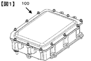
- FIG. 1 is an external perspective view of a DCDC converter device according to an embodiment of the present invention. It is a figure which shows the circuit structure of the DCDC converter apparatus concerning the Example of this invention. It is an exploded view which shows the components arrangement
- FIG. 1 is a perspective view showing an external appearance of the DCDC converter device 100.
- the DCDC converter device is applied to an electric vehicle or the like, and is a device that performs power conversion from a high voltage storage battery to a low voltage storage battery or power conversion from a low voltage storage battery to a high voltage storage battery.
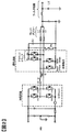
- FIG. 2 is a diagram illustrating a circuit configuration of the DCDC converter device 100.
- the DCDC converter apparatus 100 of the present embodiment is compatible with bidirectional DCDC. Therefore, the step-down circuit and the step-up circuit have a synchronous rectification configuration rather than a diode rectification.
- large current components for the switching element are employed to increase the size of the smoothing coil.
- both the HV side and the LV side have an H bridge type synchronous rectification switching circuit configuration (H1 to H4) using a MOSFET having a recovery diode.
- H1 to H4 In switching control, zero-cross switching is performed at a high switching frequency (100 kHz) using an LC series resonance circuit (Cr, Lr) to improve conversion efficiency and reduce heat loss.
- an active clamp circuit is provided to reduce loss due to circulating current during step-down operation, and to reduce the breakdown voltage of switching elements by suppressing the generation of surge voltage during switching, thereby reducing the breakdown voltage of circuit components. By downsizing, the device is downsized.
- a full-wave rectification type double current (current doubler) method was adopted.
- high output is ensured by operating a plurality of switching elements simultaneously in parallel.
- the switching elements are arranged in parallel in four elements such as SWA1 to SWA4 and SWB1 to SWB4.
- the high output is achieved by arranging the switching elements and the small reactors (L1, L2) of the smoothing reactor in parallel so as to have symmetry. As described above, by arranging the small reactors in two circuits, it is possible to reduce the size of the entire DCDC converter device as compared with the case where one large reactor is arranged.
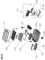
- FIG. 3 is an exploded perspective view of the DCDC converter device 100.
- the circuit components of the DCDC converter device 100 are housed in a metal (for example, aluminum die-cast) housing 101.
- a case cover 111 is fixed to the opening of the housing 101 with bolts.
- a main transformer 133, an inductor element 134, a step-down circuit unit 131 on which switching elements H1 to H4 are mounted, a step-up circuit unit 132 on which a switching element 136 is mounted, and the like are placed on the bottom surface in the housing 101. Yes.
- the main transformer 133 is the transformer Tr
- the inductor element 134 is the reactors L1 and L2 of the current doubler
- the switching element 136 is the switching elements SWA1 to SWA4 and SAWB1 to SWB4, respectively. It corresponds.
- the booster circuit unit 132 is also equipped with the switching elements S1, S2, etc. of FIG.
- Switching elements H1 to H4 are provided in the step-down circuit unit 131.
- the switching elements H1 to H4 are mounted on a metal substrate 139 on which a pattern is formed, and the back surface side of the metal substrate is fixed so as to be in close contact with the bottom surface of the housing.
- the booster circuit portion 132 on which the switching element 136 is mounted is also formed of a metal substrate.
- the control circuit board 130 is mounted with a control circuit that controls switching elements provided in the booster circuit unit 132 and the step-down circuit unit 131.
- the control circuit board 130 is fixed on a metal base plate 137.
- the base plate 137 is fixed by a plurality of support portions 101 a protruding upward from the bottom surface portion of the housing 101.
- the control circuit board 130 is disposed via the base plate 137 above the heat generating components (the main transformer 133, the inductor element 134, etc.) disposed on the bottom surface of the casing.
- the base plate 137 Since the base plate 137 is made of metal, the heat generated in the control circuit board 130 is transmitted to the support portion 101a and the housing 101.
- the base plate 137 functions as a shielding member for radiant heat from heat-generating components provided on the bottom surface of the housing, and also functions as a shield for shielding switching radiation noise from the switching element by using a copper material or the like. .
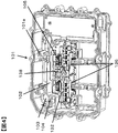
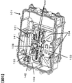
- FIG. 4 is a perspective view showing the component arrangement of the booster circuit unit 132 and the appearance of the casing (case) 101 in the DCDC converter device 100.
- FIG. 5 is a component arrangement of the booster circuit unit 132 in the DCDC converter device 100 and the booster circuit unit.
- FIG. 6 is a perspective view showing an external appearance of an LC filter circuit including an output bus bar 121 that outputs the output of 132 to the outside, an output terminal 122, a ferrite core 141, and an output filter 142, and FIG.
- the ferrite core 141 and the output filter 142 constitute an LC filter circuit installed to reduce the output noise of the DCDC converter device 100, and together with the smoothing capacitor 138 mounted on the substrate of the booster circuit unit 132, ⁇ Type LC filter circuit.
- the circuit configuration aims to reduce output noise, and is not limited to a ⁇ -type LC filter circuit.
- the output terminal 122 functions as an output terminal when power is converted from the HV side to the LV side, but functions as an input terminal when power is converted from the LV side to the HV side. In the converter of this embodiment, power conversion in both the HV side and the LV side is possible, but there is also a converter that performs power conversion only in one direction.
- a shield wall 102 formed integrally with the housing 101 is formed between the LC filter circuit and the booster circuit unit 132, and the output bus bar 121 bypasses the shield wall 102, and the booster circuit unit 132, The ferrite core 141, the output filter 142, and the output terminal 122 are electrically connected.
- the shield wall 102 switches the step-down circuit unit 131 and the booster circuit unit 132 even when the LC filter circuit, the step-down circuit unit 131, and the step-up circuit unit 132 are in the same housing of the housing 101. It is possible to prevent switching radiation noise due to the element from being superimposed on the LC filter circuit, and the noise reduction effect of the filter cannot be obtained, and it is not necessary to prepare another casing for the LC filter circuit.
- the smoothing capacitor 138 is located at a position branched from the path from the booster circuit unit 132 to the output terminal 122 and has a small effect even if it is shielded, and is provided on the substrate of the booster circuit unit 122. Therefore, the shield wall 102 is not a target to be shielded.
- the shielding effect can be further enhanced by using a conductive sealing material.
- the shield wall 102 may be formed integrally with the base plate 137.
- the base plate 137 is fixed to the housing 101 with screws (not shown), the position of the screws is the most stable position in the base plate 137. Therefore, when the shield wall 102 is formed from the base plate 137, it is desirable to install a screw hole near the shield wall 102.
- the shield wall 102 be formed from both the casing 101 and the base plate 137.
- FIG. 4 in this embodiment, it has the output terminal 122 which penetrates the through-hole 103 provided from the housing
- a protrusion 104 is formed around the through hole 103 so as to cover the output terminal, and the casing is thick. As a result, even if noise is spatially superimposed between the filter circuit and the through hole 103, it can be prevented from leaking outside.
- a GND boss 105 and a GND boss installation hole 105 a are disposed at the center of the booster circuit unit 132.
- the bus bars 123 on the substrate of the booster circuit unit 132 disposed from the two voltage conversion inductor elements 134 to the smoothing capacitor 138 can be arranged symmetrically, and the parasitic inductance values of the bus bars 123 can be made equal. Therefore, loss can be reduced.
- the casing 101 connected to the chassis is most stable in potential among the DCDC converters.
- one end of the smoothing capacitor 138 is connected to GND (ground), but the parasitic inductance between the smoothing capacitor 138 and GND can be reduced by installing the GND boss 105 in the vicinity thereof. Thereby, the noise reduction effect of the smoothing capacitor 138 can be ensured.
- the GND bus bar 124 that connects the smoothing capacitor 138 and the GND boss 105 need not be installed in parallel with the bus bar 123. Therefore, since switching noise from the bus bar 123 can be prevented from being electromagnetically coupled to the GND bus bar 124, fluctuations in the potential of the housing 101 can be prevented, and the noise level of the DCDC converter device 100 can be reduced.
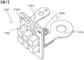
- FIG. 7 and 8 are perspective views showing the appearance of the output filter 142.
- FIG. A ceramic capacitor 142a is mounted on the filter substrate 142d, a filter output bus bar 142b for electrically connecting the capacitor 142a and the output terminal 122, and a GND bus bar 142c for electrically connecting the capacitor 142a and the housing 101.
- a fixture 142e for mechanically fixing the filter substrate 142d to the housing 101.
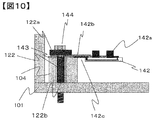
- FIG. 9 is a cross-sectional view showing the connection between the capacitor substrate 142 and the output terminal 122. Moreover, the arrow of a figure represents the direction through which the noise current which flows into a filter circuit flows.
- the filter output bus bar 142b and the GND bus bar 142c are disposed so as to face each other in the vicinity. Thereby, since the loop area formed by the filter output bus bar 142b, the filter substrate 142, and the GND bus bar 142c can be reduced, the superposition of switching noise from the step-down circuit unit 131 and the step-up circuit unit 132 can be reduced.
- the connection between the output terminal 122 and the filter substrate 142d is connected through the filter output bus bar 142b and the GND bus bar 142c.
- the large screw 144 is tightened with the bus bar 142b interposed therebetween, and the output terminal upper portion 122a is fixed to the housing 101.
- the output terminal lower part 122b the output terminal 122 and the filter output bus bar are fixed to the protruding part 104 via the insulator 143.
- the large screw 144 Because of the large current output from the DCDC converter device, the large screw 144 has a larger diameter than the screw that fixes the booster circuit unit or the like to the housing. Torque is generated by this large screw, but the bus bar can withstand this torque.
- capacitor 142a In order to ensure the performance of the capacitor 142a, a certain size is required, and a plurality of capacitors may be used. Many capacitors have terminals on both sides. When such a capacitor is used to connect to the output terminal 122 and the housing 101, the connection position with the housing tends to be far from the output terminal, and the area of the loop formed by the output terminal, the capacitor, the housing, and the wiring is large. turn into. In addition, the parasitic inductance of the filter circuit increases, and noise that is radiated from the power conversion circuit and propagated in space and electromagnetic noise that is generated due to eddy currents flowing through the housing are superimposed on the filter circuit, and the filter is filtered by electromagnetic induction. May reduce performance.
- connection position between the GND bus bar 142c and the housing 101 is closer to the output terminal 122 than the capacitor 142a and the substrate 142d, thereby reducing the loop and reducing parasitic inductance and electromagnetic induction action.
- the filter function can be ensured.
- the position close to the output terminal 122 means that the shortest distance to any part of the output terminal 122 is small in three dimensions.
- the filter output bus bar 142b and the GND bus bar 142c are arranged to face each other, noise currents flowing in the filter circuit flow to face each other, so that a U-turn current is formed between the filter output bus bar and the GND bus bar. Is done. Therefore, since the magnetic flux generated around the filter output bus bar and the magnetic flux generated around the GND bus bar cancel each other, the parasitic inductance can be reduced.
- the filter output bus bar 142b and the GND bus bar 142c are connected to the filter substrate 142d at the same side.
- the bus bars are mounted facing each other until they are connected to the board. For this reason, noise superposition and an increase in inductance can be prevented.
- the filter substrate 142d is composed of two layers, and the inner layer wiring of the substrate is mounted so that the output side connected to the filter output bus bar 142b and the GND side connected to the GND bus bar 142c are opposed to each other by the capacitor 142a. The Thereby, it is possible to prevent an increase in the parasitic inductance of the substrate pattern of the filter substrate 142d.
- the filter substrate 142d may be a multilayer substrate instead of two layers.
- the distance between the layers can be shortened, and the coupling between the output side and the GND side can be strengthened, so that an increase in parasitic inductance can be further prevented.
- the substrate 142 d of the output filter is arranged so that the surface direction thereof is along the longitudinal direction of the output terminal 122. This is because it is more space-saving to place the substrate 142d in a different direction from the substrate such as the booster circuit portion 132. In particular, as in the present embodiment, it is preferable to arrange the output circuit 122 and the substrate such as the booster circuit unit 132 so as to extend along the output terminal 122.
- the GND bus bar 142c may be connected to the upper surface of the protruding portion 104. Since the protrusion 104 has the through-hole 103 that passes through the output terminal 122, it can be connected to a position close to the output terminal 122 and is suitable for placing the substrate 142d vertically as shown in FIG.
- the base plate 137 is separated from the output filter 142, the output terminal 122, and the output bus bar 121 in addition to the shield wall 102 formed between the output filter 142 and the booster circuit unit 32.
- a shield wall 137a is formed for the purpose.
- the output filter 142 can be structured close to a separate room from the step-down circuit unit 131 and the step-up circuit unit 132 without preparing a separate housing, so that noise superimposition on the filter substrate 142d can be reduced.
- a sufficiently noise-reduced voltage can be output from the DCDC converter device.
- the DCDC converter device of the present invention can be modified into various embodiments.
- the filter substrate 142d may be mounted in parallel to the bottom surface of the housing according to the space of the housing. Also in this case, the connection portion between the GND bus bar 142d and the housing 101 is closer to the output terminal 122 than the capacitor 142a, and the loop is also reduced.
- the filter substrate 142d and the output terminal 122 may be directly connected without using the filter output bus bar 142b and the GND bus bar 142c.
- the inductance corresponding to the filter output bus bar and the GND bus bar can be reduced, and the filter substrate 142d can be mounted.
- a filter capacitor integrated with the bus bar may be used instead of mounting the ceramic capacitor on the substrate.
- the filter output bus bar and the GND bus bar facing each other and integrating them with the filter capacitor, it is possible to prevent noise from being superimposed and increase the inductance, and the same effect as when using a ceramic capacitor can be obtained. it can.
- the output terminal and the capacitor board 142 can be integrated, so that the filter output bus bar 142b and the GND bus bar 142c are omitted. May be. By omitting the bus bar, the parasitic inductance can be further reduced.
- DESCRIPTION OF SYMBOLS 100 DCDC converter apparatus, 101: Case, 102: Shield wall, 103: Through-hole, 104: Protruding part, 105: GND boss, 105a: GND boss installation hole, 111: Top cover, 121: Output bus bar, 122: Output terminal, 123: bus bar, 124: GND bus bar, 130: control circuit board, 131: step-down circuit section, 132: boost circuit section, 133: main transformer, 134: inductor element for voltage conversion, 135: power semiconductor module, 136 : H1 to H4: switching element, 137: base plate, 137a: shield wall, 141: ferrite core, 142: output filter, 142a: ceramic capacitor, 142b: filter output bus bar, 142c: GND bus bar, 142d: output filter substrate, 143: Insulator, 144: A screw.
Landscapes
- Engineering & Computer Science (AREA)
- Power Engineering (AREA)
- Life Sciences & Earth Sciences (AREA)
- Sustainable Development (AREA)
- Sustainable Energy (AREA)
- Transportation (AREA)
- Mechanical Engineering (AREA)
- Microelectronics & Electronic Packaging (AREA)
- Dc-Dc Converters (AREA)
- Electric Propulsion And Braking For Vehicles (AREA)
- Shielding Devices Or Components To Electric Or Magnetic Fields (AREA)
- Filters And Equalizers (AREA)
Abstract
Description
本発明のDCDCコンバータ装置は、様々な実施形態に変形可能である。例えば、図10に示す通り,フィルタ基板142dは、筐体のスペースに応じて筐体底面に対して平行に実装しても良い。この場合も、GNDバスバー142dと筐体101との接続部は、出力端子122にコンデンサ142aよりも近くなり、ループも小さくなる。
バスバーを省くことにより、寄生インダクタンスをさらに低減することができる。
Claims (19)
- 筐体と、
前記筐体内に設けられた回路基板と、
前記筐体に設けられた貫通孔を貫通し、前記回路基板の出力を外部に出力するまたは外部から前記回路基板に入力するための外部端子と、
を備えた電子装置において、
フィルタコンデンサを有するフィルタ手段と、
前記外部端子と前記フィルタ手段とを接続する第1の配線と、
前記フィルタ手段よりも前記外部端子に近い位置で前記筐体に接続され、前記筐体と前記フィルタ手段とを接続する第2の配線と、
を備えたことを特徴とする電子装置。 - 請求項1に記載の電子装置おいて、
前記第1の配線と前記第2の配線とは、少なくとも一部が対向して配置されることを特徴とする電子装置。 - 請求項1または2に記載の電子装置において、
前記フィルタ手段は、配線を有する基板と、当該基板に搭載され、前記配線に電気的に接続されるフィルタコンデンサを有し、
前記第1の配線及び前記第2の配線は、前記基板の面方向において前記フィルタコンデンサに対し同じ側で前記基板の配線に接続されていることを特徴とする。 - 請求項3に記載の電子装置において、
前記第1の配線及び前記第2の配線の一部が前記基板の配線と対向するように配線されていることを特徴とする電子装置。 - 請求項3または4に記載の電子装置において、
前記基板の配線は、前記フィルタコンデンサと前記第1の配線とを接続する配線と、前記フィルタコンデンサと前記第2の配線とを接続する配線とが、対向するように設けられていることを特徴とする電子装置。 - 請求項3乃至5のいずれかに記載の電子装置において、
前記回路基板と、前記フィルタ手段の基板とは、その面が異なる方向を向いていることを特徴とする電子装置。 - 筐体と、
前記筐体内に設けられた回路基板と、
前記筐体に設けられた貫通孔を貫通し、前記回路基板の出力を外部に出力するまたは外部から前記回路基板に入力するための外部端子と、
を備えた電子装置において、
コンデンサを含むフィルタ手段と、
前記外部端子と前記フィルタ手段とを接続する第1の配線と、
前記筐体と前記フィルタ手段とを接続する第2の配線と、
を有し、
前記貫通孔の周囲の筐体は、前記筐体の前記回路基板が設置された面より前記筐体内部側に向かって突出する突出部を形成し、前記第2の配線は当該突出部に接続されていることを特徴とする電子装置。 - 請求項1乃至7のいずれかに記載の電子装置において、
前記第1の配線は、フィルタ出力バスバーであり、前記第2の配線は、GNDバスバーであることを特徴とする電子装置。 - 請求項1乃至8のいずれかに記載の電子装置において、
前記フィルタ手段と前記回路基板との間にシールド手段を設けたことを特徴とする電子装置。 - 請求項1乃至9のいずれかに記載の電子装置において、
前記外部端子は、前記回路基板を筐体に固定するネジよりも大きい径を有するネジによって前記筐体に固定されており、前記第1の配線及び前記第2の配線はバスバーであることを特徴とする電子装置。 - 請求項1乃至10のいずれかにおいて、
前記回路基板は、電力を変換する電力変換回路を有してることを特徴とする電子装置。 - 筐体と、
回路基板と、
前記筐体に設けられた貫通孔を貫通し、前記回路基板の出力を外部に出力するまたは外部から前記回路基板に入力するための外部端子と、
フィルタコンデンサを有し、前記外部端子とGNDとに接続されたフィルタ手段と、
を備えた電子装置において、
前記回路基板と前記フィルタ手段とは、前記筐体内に設けられるとともに、
前記回路基板と、前記外部端子及び前記フィルタ手段との間に設けられ、電磁波をシールドするシールド手段と、
前記シールド手段を迂回して、前記回路基板と、前記外部端子及び前記フィルタ手段とを電気的に接続する配線と、
を備えたことを特徴とする電子装置。 - 請求項12に記載の電子装置において、
前記回路基板は、電力を変換する電力変換基板であることを特徴とする電子装置。 - 請求項13に記載の電子装置において、
前記電力変換基板は、スイッチング素子とダイオードとを有することを特徴とする電子装置。 - 請求項12乃至14のいずれかに記載の電子装置において、
前記配線上に、フェライトコアを有し、
前記フェライトコアと前記回路基板との間に、前記シールド手段が設けられていることを特徴とする電子装置。 - 請求項15に記載の電子装置において、
前記回路基板上に、GNDに接続された平滑化コンデンサを有し、
前記平滑化コンデンサ、前記フェライトコア及び前記フィルタ手段とによりπ型のLCフィルタを構成することを特徴とする電子装置。 - 請求項12乃至16のいずれかに記載の電子装置において、
前記シールド手段は、前記筐体と一体に形成されたシールド壁であることを特徴とする電子装置。 - 請求項12乃至17のいずれかに記載の電子装置において、
ベース基板を有し、
前記回路基板及び前記外部端子は、前記筐体と前記ベース板との間に設けられ、
前記シールド手段は、前記ベース板と一体に形成されたシールド壁であることを特徴とする電子装置。 - 請求項12乃至18のいずれかに記載の電子装置において、
前記外部端子と前記フィルタ手段との間に、シールド手段を備えたことを特徴とする電子装置。
Priority Applications (3)
| Application Number | Priority Date | Filing Date | Title |
|---|---|---|---|
| CN201280052074.9A CN103891116B (zh) | 2011-10-31 | 2012-10-26 | 电子装置 |
| US14/352,179 US9345160B2 (en) | 2011-10-31 | 2012-10-26 | Electronic device |
| DE112012004558.0T DE112012004558T5 (de) | 2011-10-31 | 2012-10-26 | Elektronische Vorrichtung |
Applications Claiming Priority (2)
| Application Number | Priority Date | Filing Date | Title |
|---|---|---|---|
| JP2011238187A JP5743851B2 (ja) | 2011-10-31 | 2011-10-31 | 電子装置 |
| JP2011-238187 | 2011-10-31 |
Publications (1)
| Publication Number | Publication Date |
|---|---|
| WO2013065586A1 true WO2013065586A1 (ja) | 2013-05-10 |
Family
ID=48191935
Family Applications (1)
| Application Number | Title | Priority Date | Filing Date |
|---|---|---|---|
| PCT/JP2012/077673 Ceased WO2013065586A1 (ja) | 2011-10-31 | 2012-10-26 | 電子装置 |
Country Status (5)
| Country | Link |
|---|---|
| US (1) | US9345160B2 (ja) |
| JP (1) | JP5743851B2 (ja) |
| CN (1) | CN103891116B (ja) |
| DE (1) | DE112012004558T5 (ja) |
| WO (1) | WO2013065586A1 (ja) |
Cited By (3)
| Publication number | Priority date | Publication date | Assignee | Title |
|---|---|---|---|---|
| CN103491742A (zh) * | 2013-10-10 | 2014-01-01 | 国电南瑞科技股份有限公司 | 一种机柜柜内布线的方法 |
| US9742082B1 (en) | 2016-08-15 | 2017-08-22 | Delta Electronics, Inc. | Connection structure of electronic components and circuit board |
| CN116390395A (zh) * | 2023-03-23 | 2023-07-04 | 深圳威迈斯新能源股份有限公司 | 功率转换模块的集成方法、功率转换模块及车载充电机 |
Families Citing this family (35)
| Publication number | Priority date | Publication date | Assignee | Title |
|---|---|---|---|---|
| JP5504219B2 (ja) * | 2011-07-27 | 2014-05-28 | 日立オートモティブシステムズ株式会社 | 電力変換装置 |
| JP6012330B2 (ja) | 2012-08-03 | 2016-10-25 | 日立オートモティブシステムズ株式会社 | Dcdcコンバータ |
| JP6101484B2 (ja) * | 2012-12-28 | 2017-03-22 | 日立オートモティブシステムズ株式会社 | Dc−dcコンバータ |
| JP6029484B2 (ja) | 2013-02-20 | 2016-11-24 | 三菱重工オートモーティブサーマルシステムズ株式会社 | インバータ一体型電動圧縮機 |
| CN105378922B (zh) * | 2013-07-11 | 2019-07-02 | 三菱电机株式会社 | 功率模块 |
| JP6298974B2 (ja) * | 2013-08-09 | 2018-03-28 | 北川工業株式会社 | 出力ノイズ低減装置 |
| WO2015053139A1 (ja) | 2013-10-07 | 2015-04-16 | 日立オートモティブシステムズ株式会社 | 電力変換装置 |
| DE102013226493B4 (de) * | 2013-12-18 | 2025-01-23 | Vitesco Technologies Germany Gmbh | Anordnung zum Potentialausgleich in einem Steuergerät |
| US9866127B2 (en) | 2014-03-03 | 2018-01-09 | Hitachi Automotive Systems, Ltd. | Electrical power converting device |
| JP6245075B2 (ja) * | 2014-05-28 | 2017-12-13 | アイシン・エィ・ダブリュ株式会社 | 車両用駆動装置 |
| JP6402563B2 (ja) * | 2014-09-30 | 2018-10-10 | 北川工業株式会社 | 出力ノイズ低減装置 |
| JP2016072504A (ja) * | 2014-09-30 | 2016-05-09 | 北川工業株式会社 | 出力ノイズ低減装置 |
| JP6218150B2 (ja) | 2015-02-25 | 2017-10-25 | 日立オートモティブシステムズ株式会社 | 電力変換装置 |
| CN106160430B (zh) * | 2015-04-13 | 2020-04-03 | 罗伯特·博世有限公司 | 电动车辆的电源转换单元及其电源母线 |
| JP2017069317A (ja) * | 2015-09-29 | 2017-04-06 | 北川工業株式会社 | ノイズ低減装置 |
| JP1557626S (ja) * | 2016-01-29 | 2016-09-05 | ||
| CN108496303B (zh) * | 2016-02-23 | 2020-06-23 | 日立汽车系统株式会社 | 电路装置 |
| RU2727730C1 (ru) * | 2017-06-15 | 2020-07-23 | Ниссан Мотор Ко., Лтд. | Устройство преобразования электроэнергии |
| DE112018003182T5 (de) | 2017-06-21 | 2020-03-05 | Sumitomo Electric Industries, Ltd. | Elektronische Schaltungsvorrichtung |
| JP7060024B2 (ja) * | 2017-11-08 | 2022-04-26 | 住友電気工業株式会社 | 電子回路装置 |
| JP6361842B1 (ja) * | 2017-12-27 | 2018-07-25 | 株式会社安川電機 | インバータ装置 |
| KR102454815B1 (ko) * | 2018-02-21 | 2022-10-17 | 삼성전자주식회사 | 브라켓과 용량성 결합을 형성하고, 상기 브라켓에 배치된 복수의 회로 기판들의 접지부들과 전기적으로 연결된 도전성 부재를 포함하는 전자 장치 |
| JP6674501B2 (ja) * | 2018-05-18 | 2020-04-01 | 本田技研工業株式会社 | 電力変換装置 |
| DE102019129498A1 (de) * | 2018-10-31 | 2020-04-30 | Hirschmann Automation And Control Gmbh | Gehäuse für einen Switch für Bahnanwendungen |
| JP7263766B2 (ja) * | 2018-12-27 | 2023-04-25 | 株式会社デンソー | 電力変換装置 |
| EP3905500A4 (en) * | 2018-12-28 | 2021-12-29 | Mitsubishi Electric Corporation | In-vehicle power conversion device |
| CN110217124A (zh) * | 2019-07-11 | 2019-09-10 | 珠海英搏尔电气股份有限公司 | 一种具有电容插板的充电机和电动车 |
| US12132410B2 (en) * | 2019-12-16 | 2024-10-29 | Hitachi Astemo, Ltd. | Power conversion device and motor |
| JP7180624B2 (ja) * | 2020-02-03 | 2022-11-30 | 株式会社デンソー | 電力変換装置 |
| CN112653311A (zh) * | 2020-12-23 | 2021-04-13 | 广州广电计量检测股份有限公司 | 一种有刷电机 |
| JP7098025B1 (ja) * | 2021-06-09 | 2022-07-08 | 三菱電機株式会社 | 電力変換装置 |
| KR102620723B1 (ko) * | 2021-09-28 | 2024-01-03 | 지에프텍 주식회사 | 전자기파 방출 저감형 트랜스포머 |
| DE102021005533A1 (de) * | 2021-11-09 | 2021-12-30 | Daimler Ag | Komponentenanordnung für ein elektrisches Hochvoltbordnetz eines Fahrzeugs |
| JP7784983B2 (ja) * | 2022-11-18 | 2025-12-12 | 三菱電機株式会社 | 電力変換装置 |
| KR102692956B1 (ko) * | 2023-07-26 | 2024-08-08 | 용인전자주식회사 | 통합 노이즈 필터 |
Citations (7)
| Publication number | Priority date | Publication date | Assignee | Title |
|---|---|---|---|---|
| JPH01218115A (ja) * | 1988-02-25 | 1989-08-31 | Nippon Ferrite Ltd | ノイズ除去フィルタ及びその製造方法 |
| JPH05328710A (ja) * | 1992-05-26 | 1993-12-10 | Fujitsu Ltd | スイッチ素子ノイズ対策方法 |
| JP2001054286A (ja) * | 1999-08-06 | 2001-02-23 | Mitsubishi Electric Corp | 電子制御基板 |
| JP2009177998A (ja) * | 2008-01-28 | 2009-08-06 | Denso Corp | 車載用電子制御装置 |
| JP2009254118A (ja) * | 2008-04-07 | 2009-10-29 | Toyota Industries Corp | 電力変換装置 |
| JP2011050160A (ja) * | 2009-08-26 | 2011-03-10 | Toyota Industries Corp | 絶縁型dc−dcコンバータ |
| JP2011103248A (ja) * | 2009-11-11 | 2011-05-26 | Zojirushi Corp | 防磁装置及びそれを備えた電磁誘導加熱式調理器 |
Family Cites Families (29)
| Publication number | Priority date | Publication date | Assignee | Title |
|---|---|---|---|---|
| US5339362A (en) * | 1992-01-07 | 1994-08-16 | Rockford Corporation | Automotive audio system |
| US6384492B1 (en) * | 1995-05-04 | 2002-05-07 | Spinel Llc | Power semiconductor packaging |
| DE19758444C2 (de) * | 1997-04-04 | 1999-12-09 | Gruendl & Hoffmann | Fluidgekühlte, Rechnereinheit - gesteuerte Baugruppe zum Schalten elektrischer Leistungen |
| US20020054480A1 (en) * | 1999-05-12 | 2002-05-09 | Ionel Jitaru | Enhanced thermal coupling for electronic boards |
| US6650559B1 (en) * | 2000-10-31 | 2003-11-18 | Fuji Electric Co., Ltd. | Power converting device |
| JP2002185339A (ja) * | 2000-12-12 | 2002-06-28 | Kokusai Denki Engineering:Kk | 放熱素子とそれを用いた高周波電子回路基板 |
| JP2003052185A (ja) * | 2001-05-30 | 2003-02-21 | Canon Inc | 電力変換器およびそれを用いる光起電力素子モジュール並びに発電装置 |
| JP3676719B2 (ja) * | 2001-10-09 | 2005-07-27 | 株式会社日立製作所 | 水冷インバータ |
| US6972957B2 (en) * | 2002-01-16 | 2005-12-06 | Rockwell Automation Technologies, Inc. | Modular power converter having fluid cooled support |
| CA2394403C (en) * | 2002-07-22 | 2012-01-10 | Celestica International Inc. | Component substrate for a printed circuit board and method of assemblying the substrate and the circuit board |
| US7026664B2 (en) * | 2003-04-24 | 2006-04-11 | Power-One, Inc. | DC-DC converter implemented in a land grid array package |
| US6849943B2 (en) * | 2003-06-06 | 2005-02-01 | Electronic Theatre Controls, Inc. | Power module package for high frequency switching system |
| DE102005016830A1 (de) * | 2004-04-14 | 2005-11-03 | Denso Corp., Kariya | Halbleitervorrichtung und Verfahren zu ihrer Herstellung |
| US7289329B2 (en) * | 2004-06-04 | 2007-10-30 | Siemens Vdo Automotive Corporation | Integration of planar transformer and/or planar inductor with power switches in power converter |
| US7248483B2 (en) * | 2004-08-19 | 2007-07-24 | Xantrex Technology, Inc. | High power density insulated metal substrate based power converter assembly with very low BUS impedance |
| JP2006180578A (ja) | 2004-12-20 | 2006-07-06 | Nippon Soken Inc | 電力変換装置 |
| US20070165376A1 (en) * | 2006-01-17 | 2007-07-19 | Norbert Bones | Three phase inverter power stage and assembly |
| JP4850564B2 (ja) * | 2006-04-06 | 2012-01-11 | 日立オートモティブシステムズ株式会社 | 電力変換装置 |
| JP4564937B2 (ja) * | 2006-04-27 | 2010-10-20 | 日立オートモティブシステムズ株式会社 | 電気回路装置及び電気回路モジュール並びに電力変換装置 |
| JP4857017B2 (ja) * | 2006-04-27 | 2012-01-18 | 日立オートモティブシステムズ株式会社 | 電力変換装置 |
| JP5227532B2 (ja) * | 2007-04-02 | 2013-07-03 | 日立オートモティブシステムズ株式会社 | インバータ回路用の半導体モジュール |
| JP4580997B2 (ja) * | 2008-03-11 | 2010-11-17 | 日立オートモティブシステムズ株式会社 | 電力変換装置 |
| US7952879B1 (en) * | 2008-04-15 | 2011-05-31 | Vlt, Inc. | System and apparatus for efficient heat removal from heat-generating electronic modules |
| JP4988665B2 (ja) * | 2008-08-06 | 2012-08-01 | 日立オートモティブシステムズ株式会社 | 半導体装置および半導体装置を用いた電力変換装置 |
| JP2010245174A (ja) * | 2009-04-02 | 2010-10-28 | Denso Corp | 電子制御ユニット及びその製造方法 |
| US8169780B2 (en) * | 2009-06-18 | 2012-05-01 | Honda Motor Co., Ltd. | Power conversion device |
| US8476989B2 (en) * | 2009-08-18 | 2013-07-02 | GM Global Technology Operations LLC | Electromagnetic interference filter for automotive electrical systems |
| US8520389B2 (en) * | 2009-12-02 | 2013-08-27 | Hamilton Sundstrand Corporation | Power semiconductor module for wide temperature applications |
| JP5158176B2 (ja) * | 2010-02-05 | 2013-03-06 | 株式会社デンソー | 電力変換装置 |
-
2011
- 2011-10-31 JP JP2011238187A patent/JP5743851B2/ja active Active
-
2012
- 2012-10-26 DE DE112012004558.0T patent/DE112012004558T5/de active Pending
- 2012-10-26 CN CN201280052074.9A patent/CN103891116B/zh active Active
- 2012-10-26 WO PCT/JP2012/077673 patent/WO2013065586A1/ja not_active Ceased
- 2012-10-26 US US14/352,179 patent/US9345160B2/en active Active
Patent Citations (7)
| Publication number | Priority date | Publication date | Assignee | Title |
|---|---|---|---|---|
| JPH01218115A (ja) * | 1988-02-25 | 1989-08-31 | Nippon Ferrite Ltd | ノイズ除去フィルタ及びその製造方法 |
| JPH05328710A (ja) * | 1992-05-26 | 1993-12-10 | Fujitsu Ltd | スイッチ素子ノイズ対策方法 |
| JP2001054286A (ja) * | 1999-08-06 | 2001-02-23 | Mitsubishi Electric Corp | 電子制御基板 |
| JP2009177998A (ja) * | 2008-01-28 | 2009-08-06 | Denso Corp | 車載用電子制御装置 |
| JP2009254118A (ja) * | 2008-04-07 | 2009-10-29 | Toyota Industries Corp | 電力変換装置 |
| JP2011050160A (ja) * | 2009-08-26 | 2011-03-10 | Toyota Industries Corp | 絶縁型dc−dcコンバータ |
| JP2011103248A (ja) * | 2009-11-11 | 2011-05-26 | Zojirushi Corp | 防磁装置及びそれを備えた電磁誘導加熱式調理器 |
Cited By (5)
| Publication number | Priority date | Publication date | Assignee | Title |
|---|---|---|---|---|
| CN103491742A (zh) * | 2013-10-10 | 2014-01-01 | 国电南瑞科技股份有限公司 | 一种机柜柜内布线的方法 |
| CN103491742B (zh) * | 2013-10-10 | 2016-01-13 | 国电南瑞科技股份有限公司 | 一种机柜柜内布线的方法 |
| US9742082B1 (en) | 2016-08-15 | 2017-08-22 | Delta Electronics, Inc. | Connection structure of electronic components and circuit board |
| TWI601334B (zh) * | 2016-08-15 | 2017-10-01 | 台達電子工業股份有限公司 | 電子元件及電路板的連接結構 |
| CN116390395A (zh) * | 2023-03-23 | 2023-07-04 | 深圳威迈斯新能源股份有限公司 | 功率转换模块的集成方法、功率转换模块及车载充电机 |
Also Published As
| Publication number | Publication date |
|---|---|
| CN103891116A (zh) | 2014-06-25 |
| JP2013099057A (ja) | 2013-05-20 |
| US20140240946A1 (en) | 2014-08-28 |
| DE112012004558T5 (de) | 2014-10-30 |
| CN103891116B (zh) | 2016-09-28 |
| JP5743851B2 (ja) | 2015-07-01 |
| US9345160B2 (en) | 2016-05-17 |
Similar Documents
| Publication | Publication Date | Title |
|---|---|---|
| JP5743851B2 (ja) | 電子装置 | |
| US9425695B2 (en) | DC-DC converter | |
| JP6897671B2 (ja) | 車載用の電力変換装置 | |
| JP6101484B2 (ja) | Dc−dcコンバータ | |
| US10128770B2 (en) | Converter and electric power conversion apparatus | |
| JP6104347B1 (ja) | 電力変換装置 | |
| JP6218150B2 (ja) | 電力変換装置 | |
| JP5327289B2 (ja) | 電力変換装置 | |
| WO2015133201A1 (ja) | 電力変換装置 | |
| WO2014033852A1 (ja) | 車載用電力変換装置 | |
| CN107306515A (zh) | 电力用电路装置 | |
| CN105580263A (zh) | 电力转换装置 | |
| JP6486443B1 (ja) | 電力変換装置 | |
| JP6719021B2 (ja) | 電力変換装置 | |
| JPWO2016080068A1 (ja) | 電力変換装置 | |
| JP6330562B2 (ja) | 電源装置 | |
| JP2014217244A (ja) | 絶縁型スイッチング電源装置および絶縁型スイッチング電源装置の製造方法 | |
| JP2013034270A (ja) | 電源装置 | |
| JP6186439B2 (ja) | Dc−dcコンバータ装置 |
Legal Events
| Date | Code | Title | Description |
|---|---|---|---|
| 121 | Ep: the epo has been informed by wipo that ep was designated in this application |
Ref document number: 12846467 Country of ref document: EP Kind code of ref document: A1 |
|
| WWE | Wipo information: entry into national phase |
Ref document number: 14352179 Country of ref document: US |
|
| WWE | Wipo information: entry into national phase |
Ref document number: 112012004558 Country of ref document: DE Ref document number: 1120120045580 Country of ref document: DE |
|
| 122 | Ep: pct application non-entry in european phase |
Ref document number: 12846467 Country of ref document: EP Kind code of ref document: A1 |