WO2013058167A1 - 固体撮像素子およびカメラシステム - Google Patents
固体撮像素子およびカメラシステム Download PDFInfo
- Publication number
- WO2013058167A1 WO2013058167A1 PCT/JP2012/076351 JP2012076351W WO2013058167A1 WO 2013058167 A1 WO2013058167 A1 WO 2013058167A1 JP 2012076351 W JP2012076351 W JP 2012076351W WO 2013058167 A1 WO2013058167 A1 WO 2013058167A1
- Authority
- WO
- WIPO (PCT)
- Prior art keywords
- amplifier
- signal
- modulator
- input
- solid
- Prior art date
Links
Images


Classifications
-
- H—ELECTRICITY
- H04—ELECTRIC COMMUNICATION TECHNIQUE
- H04N—PICTORIAL COMMUNICATION, e.g. TELEVISION
- H04N25/00—Circuitry of solid-state image sensors [SSIS]; Control thereof
- H04N25/60—Noise processing, e.g. detecting, correcting, reducing or removing noise
- H04N25/616—Noise processing, e.g. detecting, correcting, reducing or removing noise involving a correlated sampling function, e.g. correlated double sampling [CDS] or triple sampling
-
- H—ELECTRICITY
- H04—ELECTRIC COMMUNICATION TECHNIQUE
- H04N—PICTORIAL COMMUNICATION, e.g. TELEVISION
- H04N25/00—Circuitry of solid-state image sensors [SSIS]; Control thereof
- H04N25/70—SSIS architectures; Circuits associated therewith
-
- H—ELECTRICITY
- H04—ELECTRIC COMMUNICATION TECHNIQUE
- H04N—PICTORIAL COMMUNICATION, e.g. TELEVISION
- H04N25/00—Circuitry of solid-state image sensors [SSIS]; Control thereof
- H04N25/70—SSIS architectures; Circuits associated therewith
- H04N25/71—Charge-coupled device [CCD] sensors; Charge-transfer registers specially adapted for CCD sensors
- H04N25/75—Circuitry for providing, modifying or processing image signals from the pixel array
-
- H—ELECTRICITY
- H04—ELECTRIC COMMUNICATION TECHNIQUE
- H04N—PICTORIAL COMMUNICATION, e.g. TELEVISION
- H04N25/00—Circuitry of solid-state image sensors [SSIS]; Control thereof
- H04N25/70—SSIS architectures; Circuits associated therewith
- H04N25/76—Addressed sensors, e.g. MOS or CMOS sensors
-
- H—ELECTRICITY
- H04—ELECTRIC COMMUNICATION TECHNIQUE
- H04N—PICTORIAL COMMUNICATION, e.g. TELEVISION
- H04N25/00—Circuitry of solid-state image sensors [SSIS]; Control thereof
- H04N25/70—SSIS architectures; Circuits associated therewith
- H04N25/76—Addressed sensors, e.g. MOS or CMOS sensors
- H04N25/77—Pixel circuitry, e.g. memories, A/D converters, pixel amplifiers, shared circuits or shared components
Definitions
- the present invention relates to a solid-state imaging device represented by a CMOS image sensor and a camera system.
- CMOS Complementary Metal Oxide Semiconductor
- image sensors solid-state imaging devices
- the CMOS image sensor overcomes the following problems. That is, a dedicated process is required for manufacturing a CCD pixel, a plurality of power supply voltages are required for its operation, and a plurality of peripheral ICs need to be operated in combination. This is because, in the case of such a CCD, the CMOS image sensor overcomes various problems such as a very complicated system.
- the CMOS image sensor can be manufactured by using a manufacturing process similar to that of a general CMOS integrated circuit, can be driven by a single power source, and further, an analog circuit or logic using the CMOS process. Circuits can be mixed in the same chip. For this reason, the CMOS image sensor has a plurality of great merits such that the number of peripheral ICs can be reduced.
- CMOS image sensors are widely used as image sensors in imaging devices such as digital cameras, camcorders, high-end single-lens reflex cameras, surveillance cameras, in-vehicle cameras, and guidance devices, taking advantage of low power consumption and high speed. It is used. Recently, high-performance, high-quality image sensors that have on-chip functional circuit blocks such as image processing have begun to appear.
- the output circuit of a CCD is mainly a 1-channel (ch) output using an FD amplifier having a floating diffusion layer (FD).
- a CMOS image sensor has an FD amplifier for each pixel, and the output is mainly a column parallel output type in which a row in a pixel array is selected and read out in the column direction at the same time. It is. This is because it is difficult to obtain a sufficient driving capability with an FD amplifier arranged in a pixel, and therefore it is necessary to lower the data rate, and parallel processing is advantageous.
- ADC Analog-Digital-converter
- Non-Patent Document 1 A CMOS image sensor equipped with a column parallel type ADC is disclosed in Non-Patent Document 1 and Patent Document 1, for example.
- Patent Document 2 describes a converter that performs delta-sigma ( ⁇ ) AD conversion after analog CDS.
- ⁇ delta-sigma
- Non-Patent Document 2 describes a ⁇ AD converter equipped with a digital CDS function. With the technique described in Non-Patent Document 2, it is possible to reduce noise by increasing the number of oversampling.
- JP 2005-323331 A Japanese Patent No. 3904111, FIG.
- FIG.1 A 2.1M Pixels, 120frame / s CMOS Image Sensor with column-parallel ⁇ ADC Architecture, FIG.1, FIG.5
- Non-Patent Document 2 has a drawback that in an imaging state with low illuminance, it is necessary to perform gain setting in order to increase the output digital value, and noise is multiplied by gain.
- this technique has a drawback that, in a low-illumination imaging state, it is necessary to set a gain in order to increase the output digital value, and noise is multiplied by a gain.
- the solid-state imaging device reads a pixel array unit in which pixels including photodiodes that convert an optical signal into an electrical signal are arranged, and reads an analog image signal from the pixel to a signal line.
- a readout unit that processes analog pixel signals in units of columns, and the readout unit is disposed on the input side of the ⁇ modulator having a function of converting the analog pixel signal into a digital signal.
- an amplifier that amplifies the analog pixel signal read out to the signal line with a set gain and inputs the amplified signal to the ⁇ modulator.
- a camera system includes a solid-state imaging device and an optical system that forms a subject image on the solid-state imaging device, and the solid-state imaging device converts an optical signal into an electrical signal.
- a pixel array unit in which pixels including photodiodes are arranged; and a readout unit that reads out an analog image signal from the pixel to a signal line and processes the read out analog pixel signal in units of columns, and the readout unit includes: A ⁇ modulator having a function of converting the analog pixel signal into a digital signal, and an analog pixel signal which is arranged on the input side of the ⁇ modulator and read out to the signal line is amplified with a set gain. And an amplifier for inputting to the ⁇ modulator.
- FIG. 6 is a timing chart illustrating an example of operation timing of a pixel and a column circuit in the present embodiment. It is a figure for demonstrating the level diagram at the time of the high illuminance and low illuminance of the column circuit which concerns on this embodiment. It is a figure for demonstrating the level diagram at the time of high illuminance and low illuminance of the circuit of a comparative example. It is a figure which shows the other structure which applied the differential type amplifier to the amplifier in the column circuit connected to the pixel and signal line concerning this embodiment. It is a figure which shows an example of a structure of the camera system with which the solid-state image sensor which concerns on this embodiment is applied.
- FIG. 1 is a diagram illustrating a configuration example of a CMOS image sensor (solid-state imaging device) according to the present embodiment.
- the CMOS image sensor 100 includes a pixel array unit 110, a row selection circuit (Vdec) 120 as a pixel driving unit, and a column readout circuit 130 having an AD conversion function by ⁇ modulation for each column.
- Vdec row selection circuit
- the AD conversion unit is formed by a ⁇ modulator having a ⁇ modulation function, an amplifier arranged at the input stage of the ⁇ modulator, and a decimation filter circuit arranged at the output stage of the ⁇ modulator.
- a ⁇ AD converter including a ⁇ modulator and a decimation filter circuit is configured to input and output pixel signals in units of pixels.
- the CDS process is performed after AD conversion. Note that a reading portion is formed by the row selection circuit 120 and the column reading circuit 130.
- the CMOS image sensor 100 of the present embodiment can improve low-light noise by arranging an amplifier at the input stage of the ⁇ converter.
- the CMOS image sensor 100 of the present embodiment can be realized without changing the constant of the ⁇ AD converter by adjusting the AD input range to a certain width by an amplifier.
- the noise specifications of the ⁇ AD converter can be relaxed by the effect of the amplifier, and the capacitance value and the number of samplings can be reduced.
- the CMOS image sensor 100 for example, by using the same configuration as an inverter used in a ⁇ modulator as an amplifier, a value to be level-shifted can be fixedly set regardless of a gain, and an input range capable of AD conversion can be easily secured. Yes.
- a differential amplifier can also be used.
- the CMOS image sensor 100 can reduce the capacitance value of the amplifier by using a ⁇ AD converter.
- a plurality of pixel circuits 110A are arranged in a two-dimensional shape (matrix shape) of M rows ⁇ N columns.
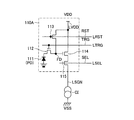
- FIG. 2 is a diagram illustrating an example of a pixel of the CMOS image sensor according to the present embodiment.
- the pixel circuit 110A includes a photodiode (PD: Photo Diode, hereinafter simply referred to as PD) 111 as a photoelectric conversion element.
- the pixel circuit 110 ⁇ / b> A has four transistors, which are a transfer transistor 112, a reset transistor 113, an amplification transistor 114, and a selection transistor 115, as active elements for the one photodiode 111.
- the transfer transistor 112, the reset transistor 113, the amplification transistor 114, and the selection transistor 115 are formed of insulated gate field effect transistors (FETs). In the example of FIG. 2, an n-channel FET is applied, but a p-channel FET can also be applied.
- FETs insulated gate field effect transistors
- the photodiode 111 photoelectrically converts incident light into charges (here, electrons) in an amount corresponding to the amount of light.
- the transfer transistor 112 is connected between the photodiode 111 and a floating diffusion FD (hereinafter sometimes simply referred to as FD) as an output node.
- the transfer transistor 112 is supplied with a transfer signal TRG as a control signal at its gate (transfer gate) through the transfer control line LTRG. Thereby, the transfer transistor 112 transfers the charges (electrons) photoelectrically converted by the photodiode 111 to the floating diffusion FD.
- the reset transistor 113 is connected between the power supply line LVDD and the floating diffusion FD, and a reset signal RST that is a control signal is given to the gate of the reset transistor 113 through the reset control line LRST. As a result, the reset transistor 113 resets the potential of the floating diffusion FD to the potential of the power supply line LVDD.
- the gate of the amplification transistor 114 is connected to the floating diffusion FD.
- the amplification transistor 114 is connected to the signal line LSGN via the selection transistor 115, and constitutes a constant current source CI and a source follower outside the pixel portion.
- a selection signal SEL which is a control signal corresponding to the address signal, is supplied to the gate of the selection transistor 115 through the selection control line LSEL, and the selection transistor 115 is turned on.
- the selection transistor 115 When the selection transistor 115 is turned on, the amplification transistor 114 amplifies the potential of the floating diffusion FD and outputs a voltage corresponding to the potential to the signal line LSGN.
- the voltage output from each pixel through the signal line LSGN is output to the column readout circuit 130.
- a reset control line LRST, a transfer control line LTRG, and a selection control line LSEL wired to the pixel array unit 110 are wired as a set for each row of the pixel array.
- M control lines for LRST, LTRG, and LSEL are provided. These reset control line LRST, transfer control line LTRG, and selection control line LSEL are driven by the row selection circuit 120.
- the row selection circuit 120 controls the operation of pixels arranged in an arbitrary row in the pixel array unit 110.
- the row selection circuit 120 controls pixels through the control lines LSEL, LRST, and LTRG.
- the column readout circuit 130 receives the data of the pixel row controlled to be read out by the row selection circuit 120 via the signal line LSGN, and transfers the data to the subsequent signal processing circuit.
- the readout circuit 130 includes an amplifier and an AD converter (a) connected to the output of each column.
- the ADC is formed by a ⁇ modulator having a ⁇ modulation function.
- the ADC by the ⁇ modulator is configured to input and output pixel signals in units of pixels.
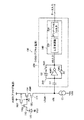
- FIG. 3 is a diagram showing a basic configuration of the column circuit connected to the pixel and the signal line according to the present embodiment.
- the column circuit 200 includes an amplifier 210 whose input is connected to the signal line LSGN, a ⁇ modulator 220 cascaded to the output of the amplifier 210, and a decimation filter circuit. .
- a ⁇ AD converter 240 is configured by the cascade-connected ⁇ modulator 220 and decimation filter circuit 230.
- the pixel 110 ⁇ / b> A is configured as an analog power supply (AVDD), the amplifier 210, the ⁇ modulator 220, and the decimation filter circuit 230 as a digital power supply (DVDD).
- AVDD analog power supply
- DVDD digital power supply
- the amplifier 210 includes an inverter type amplifier AMP1, an input capacitor C1, a variable feedback capacitor C2, a gain switch SW1, and an auto zero (AZ) switch SW2.
- the first terminal of the input capacitor C1 is connected to the signal line LSGN, and the second terminal is connected to the input terminal of the inverter type amplifier AMP1.
- a feedback capacitor C2 and a gain switch SW1 are connected in series between the output terminal and the input terminal of the inverter type amplifier AMP1.
- An auto-zero switch SW2 is connected between the output terminal and the input terminal of the inverter type amplifier AMP1.
- the auto-zero switch SW2 when the pixel 110A is reset, the auto-zero switch SW2 is turned on to cancel the offset of the inverter type amplifier AMP1 and set the input potential and the output potential to, for example, approximately (1/2) DVDD.
- the capacitance ratio C1: C2 of the input capacitance C1 and the feedback capacitance C2 is variable, the gain can be changed, and the input full scale width of the ⁇ modulator 220 which is an AD converter is constant when the gain is changed. It has a function to do.
- a differential amplifier may be used to improve power supply voltage noise resistance.
- FIG. 4 is a diagram showing a basic configuration of the ⁇ AD converter according to the present embodiment.
- FIG. 4 also shows an outline of the operation of the ⁇ AD converter 240.
- the ⁇ modulator 220 includes at least an integrator 221, a quantizer 222, a digital-to-analog converter (DAC) 223 that forms part of a feedback system to the pixel circuit 110A, and an adder 224 having a level shift function. Consists of.
- the signal obtained from the pixel circuit 110A is output as 1-bit data through the integrator 221 and the quantizer 222.
- a decimation circuit decimation filter circuit
- the decimation filter circuit 230 basically digitally adds the number “1” for each time slot.
- FIG. 4 shows a first-order ⁇ AD modulator 220 as an example, but it is desirable to apply a second-order ⁇ modulator 220A as shown in FIGS. 5 and 6, for example.
- a second-order decimation filter circuit 230 ⁇ / b> A is applied as the decimation filter circuit.
- a third-order decimation filter circuit can be applied to the decimation filter circuit.
- FIG. 5 is a diagram showing a basic configuration of the secondary ⁇ modulator according to the present embodiment.
- FIG. 6 is a diagram illustrating a specific circuit configuration of a column circuit including a ⁇ AD converter to which the secondary ⁇ modulator according to the present embodiment is applied.
- FIG. 6 shows a circuit configuration in which a pixel signal can be amplified by switching a chopper type amplifier (amplifier) and a plurality of capacitors before the input signal, which is a feature of the present technology.
- the second-order ⁇ modulator 220A is configured as an incremental type ⁇ AD converter, and includes two integrators 2211 and 2122, two DACs 2231 and 2232, and two adders 224 as ⁇ modulators. , 225.
- u represents an analog signal
- v represents a digital signal.
- the adder 224 functions as an input unit.
- the column circuit 200A shown in FIG. 6 realizes low noise even at a high gain (low illuminance) setting by disposing the amplifier 210 of the pixel signal VSL in the previous stage (input stage) of the ⁇ modulator 220A. Further, the column circuit 200A can easily adjust the input level of AD conversion by making the circuit configuration of the amplifier 210 the same as that of a part of the ⁇ modulator.
- the second-order ⁇ modulator 220A is configured as an incremental type ⁇ AD converter, and includes two integrators 2211 and 2122, two DACs 2231 and 2232 as two ⁇ modulators, and two adders 224 and 225. ing.
- a CMOS image sensor equipped with an incremental ⁇ AD converter has a noise suppression effect depending on the number of oversampling M.
- the adder 224 inputs the pixel signal VSL amplified by the amplifier 210 or a signal fed back via the DAC 2231.
- the adder 224 shifts the level of the pixel signal VSL (in the example of FIG. 6) and outputs the level to the first stage integrator 2211.
- the adder 224 includes capacitors C11 (Cs) and C12, nodes ND11 to ND13, and switches SW11 to SW14.
- the capacitor C11 is connected between the node ND11 and the node ND13
- the capacitor C12 is connected between the node ND12 and the node ND13.
- the switch SW11 is connected between the output of the amplifier 210 and the node ND11
- the switch SW12 is connected between the node ND12 and a reference potential (for example, ground) VSS.
- the switch SW13 is connected between the output of the DAC 2231 and the node ND11
- the switch SW14 is connected between the node ND12 and the supply line of the bias signal Vbias.
- the switches SW11 and SW12 are held conductive when the signal ⁇ 1 is active (for example, high level), and the switches SW13 and SW14 are held conductive when the signal ⁇ 2 is active (for example, high level).
- Signals ⁇ 1 and ⁇ 2 take complementary levels. Therefore, when the switches SW11 and SW12 are held in the conductive state, the switches SW13 and SW14 are held in the non-conductive state. On the contrary, when the switches SW13 and SW14 are held in the conductive state, the switches SW11 and SW12 are held in the non-conductive state.
- the capacitor C12 and the switch SW12 function as a level shifter.
- the first-stage integrator 2211 includes an inverter-type amplifier AMP21 that functions as an integration circuit, an input capacitor C21, a feedback capacitor C22, nodes ND21 to ND24, and switches SW21 to SW25.
- the node ND21 is connected to the output node ND13 of the adder 224.
- the inverter type amplifier AMP21 has an input terminal connected to the node ND22 and an output terminal connected to the node ND23.
- the input capacitor C21 is connected between the node ND21 and the node ND22, and the feedback capacitor C22 is connected between the node ND24 and the node ND23.
- the switch SW21 is connected between the node ND22 and the node ND24.
- the feedback capacitor C22 and the switch SW21 are connected in series between the output terminal and the input terminal of the inverter type amplifier AMP21.
- the switch SW22 is connected between the node ND21 and a reference potential (for example, ground) VSS.
- the switch SW23 is connected between the node ND21 and the node ND24, and the switch SW24 is connected between the node ND23 and the node ND24. That is, the reset switch SW24 is connected between the output terminal and the input terminal of the inverter type amplifier AMP21.
- the switch SW25 is connected to a node ND23 that is an output node of the integrator 2211 of the first stage.
- the switches SW21 and SW22 are held conductive when the signal ⁇ 1 is active (for example, high level), and the switch SW23 is held conductive when the signal ⁇ 2 is active (for example, high level). Signals ⁇ 1 and ⁇ 2 take complementary levels. Therefore, when the switches SW21 and SW22 are held in the conductive state, the switch SW23 is held in the non-conductive state. On the contrary, when the switch SW23 is held in the conductive state, the switches SW21 and SW22 are held in the non-conductive state.
- the switch SW24 is held conductive when the reset signal ⁇ RST is active (for example, high level).
- the reset signal ⁇ RST is synchronized in phase with the pixel reset signal RST.
- the switch SW25 is kept conductive when the signal ⁇ 2 is active, and causes the output of the integrator 2211 of the first stage to be input to the adder 225 of the next stage.
- the adder 225 includes a capacitor C30, a node ND30, and a switch SW30.
- the node ND30 is connected to the output switch SW25 of the first stage integrator 2211.
- the switch SW30 is connected between the output of the DAC 2232 and the node ND30, and the capacitor C30 is connected between the node ND30 and the second stage integrator 2212 of the next stage between the input node (ND31).
- the switch SW30 is held in a conductive state when the signal ⁇ 1 is active (for example, high level).
- the second stage integrator 2212 includes an inverter-type amplifier AMP31 that functions as an integration circuit, an input capacitor C31, a feedback capacitor C32, nodes ND31 to ND34, and switches SW31 to SW35.
- the node ND31 is connected to the capacitor C30 of the adder 225.
- the inverter type amplifier AMP31 has an input terminal connected to the node ND32 and an output terminal connected to the node ND33.
- the input capacitor C31 is connected between the node ND31 and the node ND32, and the feedback capacitor C32 is connected between the node ND34 and the node ND33.
- the switch SW31 is connected between the node ND32 and the node ND34.
- the feedback capacitor C32 and the switch SW31 are connected in series between the output terminal and the input terminal of the inverter type amplifier AMP31.
- the switch SW32 is connected between the node ND31 and a reference potential (for example, ground) VSS.
- the switch SW33 is connected between the node ND31 and the node ND34, and the switch SW34 is connected between the node ND33 and the node ND34. That is, the reset switch SW34 is connected between the output terminal and the input terminal of the inverter type amplifier AMP31.
- the switch SW35 is connected to a node ND33 which is an output node of the second stage integrator 2212.
- the switches SW31 and SW32 are held conductive when the signal ⁇ 2 is active (for example, high level), and the switch SW23 is held conductive when the signal ⁇ 1 is active (for example, high level). Signals ⁇ 1 and ⁇ 2 take complementary levels. Therefore, when the switches SW31 and SW32 are held in the conductive state, the switch SW33 is held in the non-conductive state. Conversely, when the switch SW33 is held in the conductive state, the switches SW31 and SW22 are held in the non-conductive state. Accordingly, the second stage integrator 2212 operates in the opposite phase to the first stage integrator 2211 and performs complementary processing.
- the switch SW34 is held conductive when the reset signal ⁇ RST is active (for example, high level).
- the reset signal ⁇ RST is synchronized in phase with the pixel reset signal RST.
- the switch SW35 is kept conductive when the signal ⁇ 1 is active, and causes the output of the integrator 2212 of the second stage to be input to one input terminal of the quantizer 222 of the next stage.
- a capacitor C40 is connected between one input terminal and a reference potential (for example, ground) VSS, and the other input terminal is connected to the reference potential VSS.
- the digital signal D222 output from the quantizer 222 is fed back to the 1-bit DAC 2232 and also fed back to the 1-bit DAC 2231 via the flip-flop FF11.
- the digital signal D222 output from the quantizer 222 is output to the decimation filter 230 at the next stage.
- the second-order decimation filter circuit 230A includes an integrator (ripple counter) 231 and an accumulator 232 that holds and adds data.
- the accumulator 232 includes an adder, a register REG, and the like.
- the column circuit 200A employs an inverter (type amplifier) as an integrator of the ⁇ ADC 220A.
- an inverter type amplifier
- the pixel signal at the time of resetting is differenced from the feedback signal from the 1-bit DACs 2231 and 2232 and is input to the first stage or second stage integrator (inverter type amplifier) 2211 and 2122. After being integrated here, it is input to a quantizer (comparator) 222, and 1 or 0 is output in comparison with a certain constant voltage.
- the output of the quantizer 222 is input to 1-bit DACs 2231 and 2232 through a feedback loop.
- the 1-bit DACs 2231 and 2232 subtract a constant voltage from the input signal in accordance with 1 and 0 from the quantizer 222 and input to the integrators (inverter type amplifiers) 2211 and 2122 through the adders 224 and 225.
- the decimation filter circuit 230A integrates the 1,0 coarse / fine wave signals in a certain time (every 7 bits in the prior art 1) and accumulates the data to convert it into a 14-bit digital output.
- bit inversion is performed and the pixel data signal is integrated in the same way to realize digital CDS, thereby reducing charge injection noise by the switch. is doing.
- a configuration of a secondary decimation filter circuit is used, but a configuration of a secondary or higher order is also possible.
- the pixel signal is halved by setting the capacitance ratio C1: C2 of the input capacitance of the amplifier 210 to the feedback capacitance to 1: 2. Input to the ⁇ modulator.
- the input width of the ⁇ ADC 220A is 0.5V.
- the capacitance ratio is 1: 0.25, thereby realizing signal amplification of 18 dB (8 times) and adjusting the AD input width to 0.5 V. To do.
- the input full scale width seen from the ⁇ ADC 220A is constant, and constants such as the capacity ratio of the ⁇ modulator can be fixed.
- the capacitance ratio is set to 1: 1, thereby realizing signal amplification of 6 dB (twice) and adjusting the input width of AD to 0.5V.
- the capacity ratio is set to 1: 0.5, thereby realizing 12 dB (4 times) signal amplification and adjusting the AD input width to 0.5V.
- FIG. 7A to 7H are timing charts showing examples of operation timings of the pixel and column circuit in the present embodiment.
- 7A shows a horizontal synchronization signal HSYNC indicating one horizontal scanning period
- FIG. 7B shows a pixel selection signal SEL
- FIG. 7C shows a pixel reset signal RST
- FIG. (D) shows the pixel transfer signal TRG.
- FIG. 7E shows the auto-zero signal AZ supplied to the switch SW2 of the amplifier 210.
- FIG. 7F shows the reset signal ⁇ R1 of the ripple counter 231 of the decimation filter circuit 230A
- FIG. 7G shows the reset signal ⁇ R2 of the accumulator 232 of the decimation filter circuit 230A.
- FIG. 7H shows the pixel signal VSL read out to the signal line LSGN.
- the floating diffusion FD is reset by the reset signal RST.
- the offset of the amplifier 210 and the operating voltage of the reset signal are determined by resetting the amplifier 210 (auto-zero AZ) (in this description, around 1/2 DVDD).
- the pixel signal VSL is read by the transfer signal (transfer pulse) TRG, and the data signal is output.
- the integrators 2211 and 2122 sample the reset signal and the data signal a plurality of times (oversampling M) and perform averaging.
- the ripple counter 231 of the decimation filter circuit 230 and the accumulator 232 are reset by the pulses ⁇ R1 and ⁇ R2.
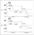
- FIG. 5 shows a level diagram of the circuit 5 at high illuminance and low illuminance.
- FIGS. 8A and 8B are diagrams for explaining level diagrams at the time of high illuminance and low illuminance of the column circuit according to the present embodiment.
- FIGS. 9A and 9B are diagrams for explaining level diagrams at the time of high illuminance and low illuminance of the circuit of the comparative example.
- the configuration of the bias (Vbias) circuit becomes complicated in order to change the level shift value with the amount of incident light.
- the inversion level at the time of auto-zero is about 1/2 DVDD regardless of the amount of incident light, as shown in FIG.
- the auto-zero signal is input to the ⁇ modulator as a reset signal, it is necessary to perform a level shift in order to match the AD input range.
- the input amplitude width is made uniform by the gain setting in the amplifier 210, but also because the ⁇ modulator 220A has the same size ratio configuration as the amplifier 210, the operating point is set to the same level.
- the level shift amount can also be set as a fixed value. Thereby, it is not particularly necessary to change the bias value Vbias, and the circuit configuration can be simplified.
- the inverter type amplifier (amplifier) has been described as an example.
- the reference voltage (Vref) is the same as the integrator (inverter type) of the ⁇ modulator 200 as shown in FIG. This can be realized by using a ratio (PMOS / NMOS).
- FIG. 10 is a diagram illustrating another configuration in which a differential amplifier is applied to the amplifier in the column circuit connected to the pixel and the signal line according to the present embodiment.
- the amplifier 210A includes a differential amplifier AMP1A, an input capacitor C1, a variable feedback capacitor C2, a gain switch SW1, an auto zero (AZ) switch SW2, and a reference voltage generation unit 211.
- a first terminal of the input capacitor C1 is connected to the signal line LSGN, and a second terminal is connected to one input terminal of the differential amplifier AMP1A.
- a feedback capacitor C2 and a gain switch SW1 are connected in series between the output terminal of the differential amplifier AMP1A and one input terminal.
- An auto zero switch SW2 is connected between the output terminal of the differential amplifier AMP1A and one input terminal.
- the reference voltage generator 211 is formed by a PMOS transistor PT1 and an NMOS transistor NT1 connected in series between the digital power supply DVDD and the reference potential VSS.
- a node ND211 is formed by a connection point between the drains of the PMOS transistor PT1 and the NMOS transistor NT1
- a node ND212 is formed by a connection point between the gates. These nodes ND211 and ND212 are connected, or connected to the other input terminal of the differential amplifier AMP1A.
- the reference voltage generator 211 supplies a reference voltage Vref generated with a size ratio (PMOS / NMOS) equivalent to that of the element forming the inverter integrator to the other input terminal of the differential amplifier AMP1A.
- the operating point is set to the same level.
- the level shift amount can also be set as a fixed value. Thereby, it is not particularly necessary to change the bias value Vbias, and the circuit configuration can be simplified.
- the power sources of the amplifiers 210 and 210A and the ⁇ AD converter are described as the same power source.
- the amplifiers 210 and 210A are a power source of digital voltage or higher, for example, an analog power source (AVDD)
- the level shift value is A fixed value can be used just by increasing it. Further, by performing auto zero, it is possible to absorb variations in the reset potential of the pixel.
- Vn 2 Vs 2 * 4 / (3M).
- Vs 2 Vsf (source follower) 2 + Vadc (AD converter) 2 is assumed.
- Amplifier thermal noise Vamp 2 for the effect of averaging due rebate effect oversampling M by analog gain G, the quantization noise VSLB 2, kTC noise Vadc 2 of ⁇ modulator can be expressed as follows.
- Vamp 2 4 / 3M * kT / 3G 2 * (1 + G) / (Cs + C1 / (1 + G))
- VLSB 2 4 / (G * (M + 1) * M) 2 *
- C11 Cs
- G C1 / C2
- VFS quantizer full-scale voltage
- k Boltzmann coefficient
- the noise characteristics are improved by the analog gain rebate effect.
- the configuration of the comparative example it is necessary to multiply the digital output by a gain, which increases not only the signal but also noise.
- the thermal noise is reduced due to the effect of oversampling by combining the amplifier 210 with the ⁇ circuit configuration. Therefore, as compared with a simple amplifier and AD converter configuration, a smaller capacity can be used, a layout mounting area can be reduced, and a reduction in pixel size can be dealt with.
- the second-order decimation filter configuration has been described, but the same effect can be obtained even in a higher-order (third-order) filter configuration.
- Low-noise noise can be improved by mounting an amplifier on a CMOS image sensor equipped with a ⁇ AD converter.
- the gain can be set without changing the constant of the ⁇ AD converter by adjusting the input signal to a constant output width by an amplifier. Since no additional circuit is required for the AD converter, the chip area can be reduced. Also, the level shift value can be fixed without depending on the amplification factor, and the circuit configuration can be facilitated.
- the noise specifications of the ⁇ AD converter can be relaxed by the effect of the amplifier, the chip area can be shrunk by reducing the capacitance value, or the power consumption can be reduced by reducing the number of samplings and reducing the clock frequency. . Further, the mounting area can be further reduced as an amplifier due to the averaging effect of ⁇ AD conversion.
- a solid-state imaging device having such an effect can be applied as an imaging device for a digital camera or a video camera.
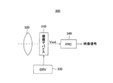
- FIG. 11 is a diagram illustrating an example of a configuration of a camera system to which the solid-state imaging device according to the embodiment of the present invention is applied.
- the camera system 300 includes an imaging device 310 to which the CMOS image sensor (solid-state imaging device) 100 according to the present embodiment can be applied. Further, the camera system 300 includes an optical system that guides incident light (images a subject image) to the pixel region of the imaging device 310, for example, a lens 320 that forms incident light (image light) on an imaging surface.
- the camera system 300 includes a drive circuit (DRV) 330 that drives the imaging device 310 and a signal processing circuit (PRC) 340 that processes an output signal of the imaging device 310.
- DUV drive circuit
- PRC signal processing circuit
- the drive circuit 330 includes a timing generator (not shown) that generates various timing signals including a start pulse and a clock pulse that drive a circuit in the imaging device 310, and drives the imaging device 310 with a predetermined timing signal. .
- the signal processing circuit 340 performs predetermined signal processing on the output signal of the imaging device 310.
- the image signal processed by the signal processing circuit 340 is recorded on a recording medium such as a memory.
- the image information recorded on the recording medium is hard copied by a printer or the like.
- the image signal processed by the signal processing circuit 340 is displayed as a moving image on a monitor including a liquid crystal display.
- the above-described solid-state imaging device 100 as the imaging device 310 in an imaging apparatus such as a digital still camera, a highly accurate camera with low power consumption can be realized.
- this technique can also take the following structures.
- a pixel array section in which pixels including photodiodes that convert optical signals into electrical signals are arranged;
- a readout unit that reads out an analog image signal from the pixel to a signal line and processes the readout analog pixel signal in units of columns;
- the readout section is A ⁇ modulator having a function of converting the analog pixel signal into a digital signal;
- a solid-state imaging device including: an amplifier that is disposed on an input side of the ⁇ modulator, amplifies an analog pixel signal read out to the signal line with a set gain, and inputs the amplified signal to the ⁇ modulator.
- the amplifier is The solid-state imaging device according to (1), wherein the gain can be set according to the input amplitude of the analog pixel signal, and amplification is performed so that an input full-scale width of the ⁇ modulator is constant.
- the ⁇ modulator is An input unit for level-shifting the pixel signal amplified by the amplifier and inputting it to an integrator; The level shift amount is set as a fixed value.
- the ⁇ modulator is At least one integrator including an inverter integrator; A quantizer that quantizes the output signal of the integrator, which is the final stage, and outputs a digital signal; A digital-to-analog converter that converts a digital signal from the quantizer into an analog signal and feeds it back to the input side of the integrator, and is formed as an n-th order modulator (n is a positive number including 1),
- the amplifier is The solid-state imaging device according to any one of (1) to (3), including an inverter type amplifier or a differential type amplifier having the same configuration as the inverter type integrator of the integrator.
- the integrator of the ⁇ modulator is Input capacitance connected to the input terminal side of the inverter type integrator, A feedback capacitor connected between the output terminal and the input terminal of the inverter integrator, The amplifier is An input capacitor connected to the input terminal side of the inverter-type amplifier;
- the solid-state imaging device according to (4) including a feedback capacitor connected between an output terminal and an input terminal of the inverter-type amplifier.
- the integrator of the ⁇ modulator is Input capacitance connected to the input terminal side of the inverter type integrator, A feedback capacitor connected between the output terminal and the input terminal of the inverter integrator,
- the amplifier is An input capacitor connected to one input terminal side of the differential amplifier;
- a feedback capacitor connected between the output terminal of the differential amplifier and one input terminal;
- a solid-state imaging device further comprising: a reference voltage generation unit that supplies, to the other input terminal of the differential amplifier, a reference voltage generated with a size ratio equivalent to an element forming the inverter integrator element.
- the amplifier is The solid-state imaging device according to (5) or (6), wherein a gain corresponding to an input amplitude of the analog pixel signal can be set by changing a capacitance ratio of the input capacitor and the feedback capacitor.
- the amplifier is The solid-state imaging device according to any one of (5) to (7), including a reset switch that resets the potentials of the output terminal and the input terminal of the amplifier to a predetermined potential.
- the pixel is Includes a reset function to reset the charge of the floating diffusion, The amplifier reset switch The solid-state imaging device according to (8), wherein the potential of the output terminal and the input terminal of the amplifier is reset while being held in a conductive state in parallel with the reset operation of the pixel.
- the reading unit The solid-state imaging device according to any one of (1) to (9), including a decimation filter circuit that multi-bits a digital signal by the ⁇ modulator.
- (11) a solid-state imaging device;
- the solid-state imaging device is A pixel array unit in which pixels including photodiodes that convert optical signals into electrical signals are arranged;
- a readout unit that reads out an analog image signal from the pixel to a signal line and processes the readout analog pixel signal in units of columns;
- the readout section is A ⁇ modulator having a function of converting the analog pixel signal into a digital signal;
- An amplifier that is arranged on the input side of the ⁇ modulator and amplifies the analog pixel signal read out to the signal line with a set gain and inputs the amplified signal to the ⁇ modulator.
- DESCRIPTION OF SYMBOLS 100 ... Solid-state image sensor, 110 ... Pixel array part, 110A ... Pixel circuit, 111 ... Photoelectric conversion element, 112 ... Transfer transistor, 113 ... Reset transistor, 114 ... Amplification Transistors 115... Selection transistor 120... Row selection circuit (pixel drive unit) 130 130 Column readout circuit 200 200 A Column circuit 210 210 A Amplifier 220 220 A ⁇ ⁇ ⁇ ⁇ modulator (, 221, 2121, 2122 ... integrator, 222 ... quantizer, 223, 2231, 2232 ... DAC, 224, 225 ... adder, 230 ... Decimation filter circuit, 240 ... ⁇ AD converter, 300 ... Camera system, 310 ... Imaging device, 320 ... Drive time , 330 ... lens (optical system), 340 ... signal processing circuit.
Abstract
Description
これはCMOSイメージセンサが次の課題を克服しているからである。
すなわち、CCD画素の製造には専用プロセスを必要とし、また、その動作には複数の電源電圧が必要であり、さらに複数の周辺ICを組み合わせて動作させる必要がある。
このようなCCDの場合、システムが非常に複雑化するといった処々の問題を、CMOSイメージセンサが克服しているからである。
このため、CMOSイメージセンサは、周辺ICの数を減らすことができるといった、大きなメリットを複数持ち合わせている。
また最近では、画像処理などの機能回路ブロックも一緒にオンチップ化した、高性能、高画質のイメージセンサも登場し始めている。
これに対して、CMOSイメージセンサは画素毎にFDアンプを持ち合わせており、その出力は、画素アレイの中のある一行を選択し、それらを同時に列方向へと読み出すような列並列出力型が主流である。
これは、画素内に配置されたFDアンプでは十分な駆動能力を得ることは難しく、したがってデータレートを下げることが必要で、並列処理が有利とされているからである。
すなわち、この技術では、CDS後のアナログ信号をサンプルするときのkTCノイズが残り、影響を小さくするためには容量値を大きくするなどチップ面積増加につながってしまう。
すなわち、この技術では、低照度の撮像状態では、出力デジタル値を大きくとるためにゲイン設定を行う必要があり、ノイズはゲイン倍されるという欠点がある。
なお、説明は以下の順序で行う。
1.固体撮像素子の構成の概要
2.読み出し回路の構成の概要
3.増幅器およびΔΣAD変換器の回路構成例
4.カメラシステムの構成例
図1は、本実施形態に係るCMOSイメージセンサ(固体撮像素子)の構成例を示す図である。
本実施形態において、カラム読み出し回路130において、CDS処理は、AD変換後に行われる。
なお、行選択回路120およびカラム読み出し回路130により読み出し部が形成される。
本実施形態のCMOSイメージセンサ100は、増幅器によりAD入力レンジを一定幅に調整することでΔΣAD変換器の定数を変更することなしに実現することができる。
CMOSイメージセンサ100は、増幅器の効果によりΔΣAD変換器のノイズスペックが緩和でき、容量値、サンプリング回数など小さくすることが可能となっている。
CMOSイメージセンサ100は、増幅器としてたとえばΔΣ変調器で使用するインバータと同じ構成を用いることでレベルシフトさせる値をゲインによらず固定で設定でき、AD変換可能な入力レンジの確保が容易になっている。また増幅器として差動型を用いることも可能である。
また、CMOSイメージセンサ100は、ΔΣAD変換器を用いることで増幅器の容量値を小さくすることが可能になっている。
そして、画素回路110Aは、この1個のフォトダイオード111に対して、転送トランジスタ112、リセットトランジスタ113、増幅トランジスタ114、および選択トランジスタ115の4つのトランジスタを能動素子として有する。
転送トランジスタ112、リセットトランジスタ113、増幅トランジスタ114、および選択トランジスタ115は、絶縁ゲート型電界効果トランジスタ(FET)により形成される。図2の例では、nチャネルのFETが適用されているが、pチャネルのFETを適用することも可能である。
なお、ここでは4トランジスタ型の画素回路の例を示しているが、選択トランジスタを有している3トランジスタ型等の適用も可能である。
転送トランジスタ112は、フォトダイオード111と出力ノードとしてのフローティングディフュージョンFD(以下、単にFDというときもある)との間に接続されている。転送トランジスタ112は、転送制御線LTRGを通じてそのゲート(転送ゲート)に制御信号である転送信号TRGが与えられる。
これにより、転送トランジスタ112は、フォトダイオード111で光電変換された電荷(電子)をフローティングディフュージョンFDに転送する。
これにより、リセットトランジスタ113は、フローティングディフュージョンFDの電位を電源ラインLVDDの電位にリセットする。
そして、選択制御線LSELを通してアドレス信号に応じた制御信号である選択信号SELが選択トランジスタ115のゲートに与えられ、選択トランジスタ115がオンする。
選択トランジスタ115がオンすると、増幅トランジスタ114はフローティングディフュージョンFDの電位を増幅してその電位に応じた電圧を信号線LSGNに出力する。信号線LSGNを通じて、各画素から出力された電圧は、カラム読み出し回路130に出力される。
これらの動作は、たとえば転送トランジスタ112、リセットトランジスタ113、および選択トランジスタ115の各ゲートが行単位で接続されていることから、1行分の各画素について同時に行われる。
LRST、LTRG、LSELの各制御線はそれぞれM本ずつ設けられている。
これらのリセット制御線LRST、転送制御線LTRG、および選択制御線LSELは、行選択回路120により駆動される。
読み出し回路130は、各カラムに増幅器およびその出力に接続されたAD変換器(アを含む。
ADCは、ΔΣ変調機能を有するΔΣ変調器により形成され、たとえばΔΣ変調器によるADCは画素単位に画素信号を入出力するように構成されている。
図3は、本実施形態に係る画素と信号線に接続されたカラム回路の基本構成を示す図である。
そして、縦続接続されたΔΣ変調器220およびデシメーションフィルタ回路230によりΔΣAD変換器240が構成される。
図3の例では、画素110Aをアナログ電源(AVDD)、増幅器210、ΔΣ変調器220、デシメーションフィルタ回路230をデジタル電源(DVDD)とした構成で示している。
後述するように画素の振幅レベルによっては、増幅器をデジタル電圧以上の電源、たとえばアナログ電源とすることでも対応可能である。
入力容量C1の第1端子が信号線LSGNに接続され、第2端子がインバータ型アンプAMP1の入力端子に接続されている。
フィードバック容量C2とゲインスイッチSW1がインバータ型アンプAMP1の出力端子と入力端子間に直列に接続されている。
オートゼロ用スイッチSW2がインバータ型アンプAMP1の出力端子と入力端子間に接続されている。
増幅器210は、入力容量C1とフィードバック容量C2の容量比C1:C2が可変で、ゲインを変更可能であり、かつ、ゲイン変更時にAD変換器であるΔΣ変調器220の入力フルスケール幅を一定とする機能を有している。
また、別の実施形態として電源電圧ノイズ耐性向上のため差動型の増幅器を用いてもよい。
図4は、ΔΣAD変換器240の動作概要を併せて示している。
ΔΣ変調器220においては、画素回路110Aから得られた信号は積分器221、量子化器222を通して1ビットデータとして出力される。
ΔΣAD変換器240は、量子化器の出力側に、1ビットデータを多ビット化するデシメーション回路(デシメーションフィルタ回路)230が配置される。
デシメーションフィルタ回路230は、基本的にタイムスロット毎に“1”の数をデジタル加算する。
また、図5および図6の例では、デシメーションフィルタ回路としては、2次のデシメーションフィルタ回路230Aが適用されている。ただし、デシメーションフィルタ回路は3次のデシメーションフィルタ回路を適用することも可能である。
図5は、本実施形態に係る2次のΔΣ変調器の基本構成を示す図である。
図6は、本実施形態に係る2次のΔΣ変調器を適用したΔΣAD変換器を含むカラム回路の具体的な回路構成を示す図である。
図6は、本技術の特徴である入力信号の前段にチョッパ型の増幅器(アンプ)と複数の容量を切り替えることで画素信号を増幅することが可能になる回路構成を示している。
なお、図5において、uはアナログ信号を、vはデジタル信号を示している。
加算器224は入力部として機能する。
また、カラム回路200Aは、増幅器210の回路構成とΔΣ変調器の一部の回路構成を同様にすることで、AD変換の入力レベルの調整を容易にすることができる。
2次のΔΣ変調器220Aは、インクリメンタル型ΔΣAD変換器として構成され、ΔΣ変調器としての2つの積分器2211,2212、2つのDAC2231,2232、および2つの加算器224,225を含んで構成されている。
インクリメンタル型ΔΣAD変換器を搭載したCMOSイメージセンサではオーバーサンプリング回数Mによってノイズ抑制効果をもつ。
加算器224は、増幅器210による画素信号VSLを入力する場合には、そのレベルをレベルシフト(図6の例ではレベルダウン)させて第1ステージの積分器2211に出力する。
容量C11はノードND11とノードND13との間に接続され、容量C12はノードND12とノードND13との間に接続されている。
スイッチSW11は増幅器210の出力とノードND11間に接続され、スイッチSW12はノードND12と基準電位(たとえばグランド)VSSとの間に接続されている。
スイッチSW13はDAC2231の出力とノードND11との間に接続され、スイッチSW14はノードND12とバイアス信号Vbiasの供給ラインとの間に接続されている。
スイッチSW11およびSW12は信号Φ1がアクティブ(たとえばハイレベル)のときに導通状態に保持され、スイッチSW13およびSW14は信号Φ2がアクティブ(たとえばハイレベル)のときに導通状態に保持される。
信号Φ1と信号Φ2は相補的なレベルをとる。したがって、スイッチSW11およびSW12が導通状態に保持されているときは、スイッチSW13およびSW14は非導通状態に保持される。逆に、スイッチSW13およびSW14が導通状態に保持されているときは、スイッチSW11およびSW12は非導通状態に保持される。
加算器224において、容量C12とスイッチSW12はレベルシフタとして機能する。
ノードND21は加算器224の出力ノードND13に接続されている。
インバータ型アンプAMP21は、入力端子がノードND22に接続され、出力端子がノードND23に接続されている。
入力容量C21はノードND21とノードND22との間に接続され、フィードバック容量C22はノードND24とノードND23との間に接続されている。
スイッチSW21はノードND22とノードND24との間に接続されている。すなわち、フィードバック容量C22とスイッチSW21はインバータ型アンプAMP21の出力端子と入力端子との間に直列に接続されている。
スイッチSW22はノードND21と基準電位(たとえばグランド)VSSとの間に接続されている。
スイッチSW23はノードND21とノードND24との間に接続され、スイッチSW24はノードND23とノードND24との間に接続されている。すなわち、リセット用のスイッチSW24はインバータ型アンプAMP21の出力端子と入力端子との間に接続されている。
スイッチSW25は第1ステージの積分器2211の出力ノードであるノードND23に接続されている。
スイッチSW21およびSW22は信号Φ1がアクティブ(たとえばハイレベル)のときに導通状態に保持され、スイッチSW23は信号Φ2がアクティブ(たとえばハイレベル)のときに導通状態に保持される。
信号Φ1と信号Φ2は相補的なレベルをとる。したがって、スイッチSW21およびSW22が導通状態に保持されているときは、スイッチSW23は非導通状態に保持される。逆に、スイッチSW23が導通状態に保持されているときは、スイッチSW21およびSW22は非導通状態に保持される。
スイッチSW24はリセット信号ΦRSTがアクティブ(たとえばハイレベル)のときに導通状態に保持される。リセット信号ΦRSTは画素のリセット信号RSTと同相で同期がとられている。
スイッチSW25は、信号Φ2がアクティブのときに導通状態に保持され、第1ステージの積分器2211の出力を次段の加算器225に入力させる。
ノードND30は、第1ステージの積分器2211の出力スイッチSW25に接続されている。
スイッチSW30は、DAC2232の出力とノードND30との間に接続され、容量C30はノードND30と次段の第2ステージの積分器2212に入力ノード(ND31)との間に接続されている。
スイッチSW30は、信号Φ1がアクティブ(たとえばハイレベル)のときに導通状態に保持される。
ノードND31は加算器225の容量C30に接続されている。
インバータ型アンプAMP31は、入力端子がノードND32に接続され、出力端子がノードND33に接続されている。
入力容量C31はノードND31とノードND32との間に接続され、フィードバック容量C32はノードND34とノードND33との間に接続されている。
スイッチSW31はノードND32とノードND34との間に接続されている。すなわち、フィードバック容量C32とスイッチSW31はインバータ型アンプAMP31の出力端子と入力端子との間に直列に接続されている。
スイッチSW32はノードND31と基準電位(たとえばグランド)VSSとの間に接続されている。
スイッチSW33はノードND31とノードND34との間に接続され、スイッチSW34はノードND33とノードND34との間に接続されている。すなわち、リセット用のスイッチSW34はインバータ型アンプAMP31の出力端子と入力端子との間に接続されている。
スイッチSW35は第2ステージの積分器2212の出力ノードであるノードND33に接続されている。
スイッチSW31およびSW32は信号Φ2がアクティブ(たとえばハイレベル)のときに導通状態に保持され、スイッチSW23は信号Φ1がアクティブ(たとえばハイレベル)のときに導通状態に保持される。
信号Φ1と信号Φ2は相補的なレベルをとる。したがって、スイッチSW31およびSW32が導通状態に保持されているときは、スイッチSW33は非導通状態に保持される。逆に、スイッチSW33が導通状態に保持されているときは、スイッチSW31およびSW22は非導通状態に保持される。
したがって、第2ステージの積分器2212は第1ステージの積分器2211と逆相で動作し、相補的な処理を行う。
スイッチSW34はリセット信号ΦRSTがアクティブ(たとえばハイレベル)のときに導通状態に保持される。リセット信号ΦRSTは画素のリセット信号RSTと同相で同期がとられている。
スイッチSW35は、信号Φ1がアクティブのときに導通状態に保持され、第2ステージの積分器2212の出力を次段の量子化器222の一方の入力端子に入力させる。
量子化器222から出力されるデジタル信号D222は、1ビットDAC2232にフィードバックされ、また、フリップフロップFF11を介して1ビットDAC2231にフィードバックされる。
量子化器222から出力されるデジタル信号D222は、次段のデシメーションフィルタ230に出力される。
リセット時の画素信号は1ビットDAC2231,2232からのフィードバック信号との差をとられ第1ステージまたは第2ステージの積分器(インバータ型アンプ))2211,2212に入力される。
ここで積分された後、量子化器(コンパレータ)222に入力され、ある一定電圧との比較で1または0を出力する。そしてこの量子化器222の出力はフィードバックループを通って、1ビットDAC2231,2232に入力される。
1ビットDAC2231,2232は、量子化器222からの1、0に応じて入力信号から一定電圧を減算し加算器224,225を介して積分器(インバータ型アンプ)2211,2212に入力する。
また、デシメーションフィルタ230で画素のリセット信号を粗密信号化として累積積分した後に、ビット反転を行い、画素のデータ信号を同様に積算することでデジタルCDSを実現し、スイッチによるチャージインジェクションノイズ低減を実現している。
本実施形態では2次のデシメーションフィルタ回路の構成としたが、2次以上での構成も可能である。
次に、ΔΣADC200Aの入力段に配置される増幅器210のアナログゲインとΔΣADC200Aの入力レンジについて説明する。
表1に本実施形態の増幅器210におけるアナログゲイン設定例を示す。

また、入射光量の少ない低照度時(入力振幅が125mV)には容量比を1:0.25とすることで18dB(8倍)の信号増幅を実現しADの入力幅を0.5Vに調整する。
つまり、ゲイン変更時にもΔΣADC220Aからみた入力フルスケール幅は一定となり、ΔΣモジュレータの容量比などの定数は固定で構成することができる。
なお、表1の例では、入力振幅が500mVのときには容量比を1:1とすることで6dB(2倍)の信号増幅を実現しADの入力幅を0.5Vに調整する。
入力振幅が250mVのときには容量比を1:0.5とすることで12dB(4倍)の信号増幅を実現しADの入力幅を0.5Vに調整する。
図7の(A)~(H)は、本実施形態における画素およびカラム回路の動作タイミング例を示すタイミングチャートである。
図7の(A)は1水平走査期間を示す水平同期信号HSYNCを、図7の(B)は画素の選択信号SELを、図7の(C)は画素のリセット信号RSTを、図7の(D)は画素の転送信号TRGをそれぞれ示している。
図7の(E)は増幅器210のスイッチSW2に供給されるオートゼロ信号AZを示している。図7(F)はデシメーションフィルタ回路230Aのリップルカウンタ231のリセット信号ΦR1を、図7の(G)はデシメーションフィルタ回路230Aのアキュムレータ232のリセット信号ΦR2をそれぞれ示している。図7の(H)は信号線LSGNに読み出される画素信号VSLを示している。
その後、転送信号(転送パルス)TRGによって画素信号VSLを読み出し、データ信号の出力を行う。
ΔΣADC220Aとしては積分器2211,2212でリセット信号、データ信号を複数回サンプリング(オーバーサンプリングM)し平均化を行う。
その際に、パルスφR1、φR2によってデシメーションフィルタ回路230のリップルカウンタ231のリセット、累算器(アキュミュレータ)232のリセットを行う。
次に、本実施形態に係るカラム回路の高照度時と低照度時のレベルダイヤについて説明する。ここでは、比較例として非特許文献2のFIG.5の回路の高照度時と低照度時のレベルダイヤについて示す。
図9の(A)および(B)は、比較例の回路の高照度時と低照度時のレベルダイヤについて説明するための図である。
これを回避するためにレベルシフト値を入射光量で変動させる手法をとるにはバイアス(Vbias)回路の構成が複雑化してしまう。
本実施形態では、増幅器210に積分器2211,2212と同じサイズ比(PMOS/NMOS)を使用することで、図8に示すように、オートゼロ時の反転レベルは入射光量にかかわらず1/2DVDD付近に設定される。
オートゼロ時の信号をリセット信号としてΔΣ変調器に入れる際に、ADの入力レンジ範囲に揃えるためにレベルシフトを行う必要がある。
本実施形態では、増幅器210でのゲイン設定により入力振幅幅は揃えられているだけでなく、ΔΣ変調器220Aは増幅器210と同じサイズ比の構成のため動作点も同程度に設定されることから、レベルシフト量も固定値として設定できる。
これにより、バイアス値Vbiasの変更も特に不要となり回路構成をシンプルにすることが可能になる。
増幅器210Aは、差動型アンプAMP1A、入力容量C1、可変のフィードバック容量C2、ゲインスイッチSW1、オートゼロ(AZ)用スイッチSW2、および基準電圧生成部211を含んで構成されている。
入力容量C1の第1端子が信号線LSGNに接続され、第2端子が差動型アンプAMP1Aの一方の入力端子に接続されている。
フィードバック容量C2とゲインスイッチSW1が差動型アンプAMP1Aの出力端子と一方の入力端子間に直列に接続されている。
オートゼロ用スイッチSW2が差動型アンプAMP1Aの出力端子と一方の入力端子間に接続されている。
基準電圧生成部211は、差動型アンプAMP1Aの他方の入力端子に、上記インバータ型積分器を形成する素子と同等のサイズ比(PMOS/NMOS)をもって生成した基準電圧Vrefを供給する。
これにより、バイアス値Vbiasの変更も特に不要となり回路構成をシンプルにすることが可能になる。
またオートゼロを行うことで画素のリセット電位のバラツキも吸収することが可能になる。
また、本実施形態に係るカラム回路の構成ではインクリメンタル型による平均化に加えてアナログゲインによりのノイズの低減効果が期待できる。
インクリメンタル型での量子化ノイズ、kTCノイズおよび増幅器でのノイズの算出について説明する。
2次のΔΣ変調器とデシメーションフィルタ回路を用いた場合のトータルノイズVnはオーバーサンプリングMによる平均化により次のように表される。
ここでVs2=Vsf(ソースフォロア)2+Vadc(AD変換器)2とする。
VLSB2=4/(G*(M+1)*M)2*VFS2
Vadc2=4/(3G2*M)*5*k*T/Cs
ここでC11=Cs,G=C1/C2,VFS(量子化器フルスケール電圧)、k(ボルツマン係数)とする。
一方、比較例の構成では、デジタル出力をゲイン倍する必要があり信号だけでなくノイズまで増加することになる。
本実施形態では、増幅器210についてもΔΣ回路構成と組み合わせることでオーバーサンプリングの効果のため熱雑音が低減される。
よって、単純な増幅器およびAD変換器の構成に比較して、より小さな容量を用いることができレイアウトの実装面積が小さくなるコスト低減効果や微細化画素に対する対応も可能になる。
本実施形態では、2次のデシメーションフィルタ構成で説明したが、より高次(3次)のフィルタ構成においても同様な効果を得ることができる。
ΔΣAD変換器を搭載したCMOSイメージセンサに増幅器を搭載することで低照度のノイズを改善することができる。
入力信号に対し増幅器により一定出力幅に調整することでΔΣAD変換器の定数を変更することなしにゲイン設定ができる。AD変換部への追加回路が必要なくなるため、チップ面積を小さくすることができる。またレベルシフトの値も増幅率に依存せず固定とすることができ、回路構成を容易にできる。
増幅器の効果によりΔΣAD変換器のノイズスペックが緩和でき、容量値を小さくするできることによるチップ面積のシュリンク、またはサンプリング回数を少なくしクロック周波数を落とすことができることによる低消費電力化を実現することができる。
また、増幅器としてもΔΣAD変換の平均化の効果によりより実装面積を小さくすることができる。
図11は、本発明の実施形態に係る固体撮像素子が適用されるカメラシステムの構成の一例を示す図である。
さらに、カメラシステム300は、この撮像デバイス310の画素領域に入射光を導く(被写体像を結像する)光学系、たとえば入射光(像光)を撮像面上に結像させるレンズ320を有する。
カメラシステム300は、撮像デバイス310を駆動する駆動回路(DRV)330と、撮像デバイス310の出力信号を処理する信号処理回路(PRC)340と、を有する。
信号処理回路340で処理された画像信号は、たとえばメモリなどの記録媒体に記録される。記録媒体に記録された画像情報は、プリンタなどによってハードコピーされる。また、信号処理回路340で処理された画像信号を液晶ディスプレイ等からなるモニターに動画として映し出される。
(1)光信号を電気信号に変換するフォトダイオードを含む画素が配列された画素アレイ部と、
上記画素からのアナログ画像信号を信号線に読み出し、読み出したアナログ画素信号をカラム単位で処理する読み出し部と、を有し、
上記読み出し部は、
上記アナログ画素信号をデジタル信号に変換する機能を有するΔΣ変調器と、
上記ΔΣ変調器の入力側に配置され、上記信号線に読み出されたアナログ画素信号を設定されるゲインをもって増幅して上記ΔΣ変調器に入力する増幅器と、を含む
固体撮像素子。
(2)上記増幅器は、
上記アナログ画素信号の入力振幅に応じたゲイン設定が可能で、上記ΔΣ変調器の入力フルスケール幅が一定となるように増幅を行う
上記(1)記載の固体撮像素子。
(3)上記ΔΣ変調器は、
上記増幅器で増幅された上記画素信号をレベルシフトして積分器に入力する入力部を有し、
上記レベルシフト量は、固定値として設定される
上記(2)記載の固体撮像素子。
(4)上記ΔΣ変調器は、
インバータ型積分器を含む少なくとも一つの積分器と、
最終段となる上記積分器の出力信号を量子化してデジタル信号を出力する量子化器と、
上記量子化器によるデジタル信号をアナログ信号に変換し、上記積分器の入力側に帰還させるデジタルアナログ変換器と、を含む、n(nは1を含む正数)次の変調器として形成され、
上記増幅器は、
上記積分器の上記インバータ型積分器と同じ構成のインバータ型アンプまたは差動型アンプを含む
上記(1)から(3)のいずれか一に記載の固体撮像素子。
(5)上記ΔΣ変調器の積分器は、
上記インバータ型積分器の入力端子側に接続された入力容量と、
上記インバータ型積分器の出力端子と入力端子間に接続されたフィードバック容量と、を含み、
上記増幅器は、
上記インバータ型アンプの入力端子側に接続された入力容量と、
上記インバータ型アンプの出力端子と入力端子間に接続されたフィードバック容量と、を含む
上記(4)記載の固体撮像素子。
(6)上記ΔΣ変調器の積分器は、
上記インバータ型積分器の入力端子側に接続された入力容量と、
上記インバータ型積分器の出力端子と入力端子間に接続されたフィードバック容量と、を含み、
上記増幅器は、
上記差動型アンプの一方の入力端子側に接続された入力容量と、
上記差動型アンプの出力端子と一方の入力端子間に接続されたフィードバック容量と、
上記差動型アンプの他方の入力端子に、上記インバータ型積分器を形成する素子と同等のサイズ比をもって生成した基準電圧を供給する基準電圧生成部と、を含む
上記(4)記載の固体撮像素子。
(7)上記増幅器は、
上記入力容量と上記フィードバック容量の容量比を変更することにより、上記アナログ画素信号の入力振幅に応じたゲインを設定可能である
上記(5)または(6)記載の固体撮像素子。
(8)上記増幅器は、
上記アンプの出力端子と入力端子の電位を所定電位にリセットするリセット用スイッチを含む
上記(5)から(7)のいずれか一に記載の固体撮像素子。
(9)上記画素は、
フローティングディフュージョンの電荷をリセットするリセット機能を含み、
上記増幅器のリセット用スイッチは、
上記画素のリセット動作に並行して導通状態に保持されて、上記アンプの出力端子と入力端子の電位のリセットを行う
上記(8)記載の固体撮像素子。
(10)上記読み出し部は、
上記ΔΣ変調器によるデジタル信号を多ビット化するデシメーションフィルタ回路を含む
上記(1)から(9)のいずれか一に記載の固体撮像素子。
(11)固体撮像素子と、
上記固体撮像素子に被写体像を結像する光学系と、を有し、
上記固体撮像素子は、
光信号を電気信号に変換するフォトダイオードを含む画素が配列された画素アレイ部と、
上記画素からのアナログ画像信号を信号線に読み出し、読み出したアナログ画素信号をカラム単位で処理する読み出し部と、を有し、
上記読み出し部は、
上記アナログ画素信号をデジタル信号に変換する機能を有するΔΣ変調器と、
上記ΔΣ変調器の入力側に配置され、上記信号線に読み出されたアナログ画素信号を設定されるゲインをもって増幅して上記ΔΣ変調器に入力する増幅器と、を含む
カメラシステム。
Claims (11)
- 光信号を電気信号に変換するフォトダイオードを含む画素が配列された画素アレイ部と、
上記画素からのアナログ画像信号を信号線に読み出し、読み出したアナログ画素信号をカラム単位で処理する読み出し部と、を有し、
上記読み出し部は、
上記アナログ画素信号をデジタル信号に変換する機能を有するΔΣ変調器と、
上記ΔΣ変調器の入力側に配置され、上記信号線に読み出されたアナログ画素信号を設定されるゲインをもって増幅して上記ΔΣ変調器に入力する増幅器と、を含む
固体撮像素子。 - 上記増幅器は、
上記アナログ画素信号の入力振幅に応じたゲイン設定が可能で、上記ΔΣ変調器の入力フルスケール幅が一定となるように増幅を行う
請求項1記載の固体撮像素子。 - 上記ΔΣ変調器は、
上記増幅器で増幅された上記画素信号をレベルシフトして積分器に入力する入力部を有し、
上記レベルシフト量は、固定値として設定される
請求項2記載の固体撮像素子。 - 上記ΔΣ変調器は、
インバータ型積分器を含む少なくとも一つの積分器と、
最終段となる上記積分器の出力信号を量子化してデジタル信号を出力する量子化器と、
上記量子化器によるデジタル信号をアナログ信号に変換し、上記積分器の入力側に帰還させるデジタルアナログ変換器と、を含む、n(nは1を含む正数)次の変調器として形成され、
上記増幅器は、
上記積分器の上記インバータ型積分器と同じ構成のインバータ型アンプまたは差動型アンプを含む
請求項1記載の固体撮像素子。 - 上記ΔΣ変調器の積分器は、
上記インバータ型積分器の入力端子側に接続された入力容量と、
上記インバータ型積分器の出力端子と入力端子間に接続されたフィードバック容量と、を含み、
上記増幅器は、
上記インバータ型アンプの入力端子側に接続された入力容量と、
上記インバータ型アンプの出力端子と入力端子間に接続されたフィードバック容量と、を含む
請求項4記載の固体撮像素子。 - 上記ΔΣ変調器の積分器は、
上記インバータ型積分器の入力端子側に接続された入力容量と、
上記インバータ型積分器の出力端子と入力端子間に接続されたフィードバック容量と、を含み、
上記増幅器は、
上記差動型アンプの一方の入力端子側に接続された入力容量と、
上記差動型アンプの出力端子と一方の入力端子間に接続されたフィードバック容量と、
上記差動型アンプの他方の入力端子に、上記インバータ型積分器を形成する素子と同等のサイズ比をもって生成した基準電圧を供給する基準電圧生成部と、を含む
請求項4記載の固体撮像素子。 - 上記増幅器は、
上記入力容量と上記フィードバック容量の容量比を変更することにより、上記アナログ画素信号の入力振幅に応じたゲインを設定可能である
請求項5または請求項6記載の固体撮像素子。 - 上記増幅器は、
上記アンプの出力端子と入力端子の電位を所定電位にリセットするリセット用スイッチを含む
請求項5または請求項6記載の固体撮像素子。 - 上記画素は、
フローティングディフュージョンの電荷をリセットするリセット機能を含み、
上記増幅器のリセット用スイッチは、
上記画素のリセット動作に並行して導通状態に保持されて、上記アンプの出力端子と入力端子の電位のリセットを行う
請求項8記載の固体撮像素子。 - 上記読み出し部は、
上記ΔΣ変調器のデジタル信号を多ビット化するデシメーションフィルタ回路を含む
請求項1記載の固体撮像素子。 - 固体撮像素子と、
上記固体撮像素子に被写体像を結像する光学系と、を有し、
上記固体撮像素子は、
光信号を電気信号に変換するフォトダイオードを含む画素が配列された画素アレイ部と、
上記画素からのアナログ画像信号を信号線に読み出し、読み出したアナログ画素信号をカラム単位で処理する読み出し部と、を有し、
上記読み出し部は、
上記アナログ画素信号をデジタル信号に変換する機能を有するΔΣ変調器と、
上記ΔΣ変調器の入力側に配置され、上記信号線に読み出されたアナログ画素信号を設定されるゲインをもって増幅して上記ΔΣ変調器に入力する増幅器と、を含む
カメラシステム。
Priority Applications (5)
| Application Number | Priority Date | Filing Date | Title |
|---|---|---|---|
| KR1020147008078A KR101969189B1 (ko) | 2011-10-20 | 2012-10-11 | 고체 촬상 소자 및 카메라 시스템 |
| US14/348,727 US9451189B2 (en) | 2011-10-20 | 2012-10-11 | Solid-state image sensor and camera system |
| EP12842515.4A EP2770732B1 (en) | 2011-10-20 | 2012-10-11 | Solid-state image sensor and camera system |
| CN201280050010.5A CN103875238B (zh) | 2011-10-20 | 2012-10-11 | 固态图像传感器和相机系统 |
| US15/238,154 US9843747B2 (en) | 2011-10-20 | 2016-08-16 | Solid-state image sensor and camera system |
Applications Claiming Priority (2)
| Application Number | Priority Date | Filing Date | Title |
|---|---|---|---|
| JP2011-230676 | 2011-10-20 | ||
| JP2011230676A JP5887827B2 (ja) | 2011-10-20 | 2011-10-20 | 固体撮像素子およびカメラシステム |
Related Child Applications (2)
| Application Number | Title | Priority Date | Filing Date |
|---|---|---|---|
| US14/348,727 A-371-Of-International US9451189B2 (en) | 2011-10-20 | 2012-10-11 | Solid-state image sensor and camera system |
| US15/238,154 Continuation US9843747B2 (en) | 2011-10-20 | 2016-08-16 | Solid-state image sensor and camera system |
Publications (1)
| Publication Number | Publication Date |
|---|---|
| WO2013058167A1 true WO2013058167A1 (ja) | 2013-04-25 |
Family
ID=48140815
Family Applications (1)
| Application Number | Title | Priority Date | Filing Date |
|---|---|---|---|
| PCT/JP2012/076351 WO2013058167A1 (ja) | 2011-10-20 | 2012-10-11 | 固体撮像素子およびカメラシステム |
Country Status (6)
| Country | Link |
|---|---|
| US (2) | US9451189B2 (ja) |
| EP (1) | EP2770732B1 (ja) |
| JP (1) | JP5887827B2 (ja) |
| KR (1) | KR101969189B1 (ja) |
| CN (2) | CN103875238B (ja) |
| WO (1) | WO2013058167A1 (ja) |
Cited By (2)
| Publication number | Priority date | Publication date | Assignee | Title |
|---|---|---|---|---|
| CN112798603A (zh) * | 2021-01-06 | 2021-05-14 | 深圳技术大学 | 一种成像系统及其成像方法 |
| US11653121B2 (en) | 2021-02-04 | 2023-05-16 | Canon Kabushiki Kaisha | Photoelectric conversion apparatus, A/D converter, and equipment |
Families Citing this family (11)
| Publication number | Priority date | Publication date | Assignee | Title |
|---|---|---|---|---|
| US9106918B2 (en) | 2012-01-20 | 2015-08-11 | Sony Corporation | Coefficient coding harmonization in HEVC |
| KR101689665B1 (ko) | 2014-07-04 | 2016-12-26 | 삼성전자 주식회사 | 이미지 센서, 이미지 센싱 방법, 그리고 이미지 센서를 포함하는 이미지 촬영 장치 |
| CN107360738B (zh) * | 2015-04-03 | 2020-10-27 | 索尼半导体解决方案公司 | 固态成像元件、成像设备和电子器械 |
| KR102392791B1 (ko) * | 2015-11-04 | 2022-05-02 | 삼성전자주식회사 | 이미지 센서, 이를 포함하는 전자 장치 및 이의 동작 방법 |
| WO2021138838A1 (zh) * | 2020-01-08 | 2021-07-15 | 华为技术有限公司 | 一种图像读取电路、图像传感器以及终端设备 |
| JP7405653B2 (ja) * | 2020-03-11 | 2023-12-26 | Tianma Japan株式会社 | イメージセンサ |
| CN112714268B (zh) * | 2020-08-21 | 2022-02-08 | 深圳市汇顶科技股份有限公司 | 图像传感器、指纹检测装置和电子设备 |
| WO2022036713A1 (zh) | 2020-08-21 | 2022-02-24 | 深圳市汇顶科技股份有限公司 | 图像传感器、指纹检测装置和电子设备 |
| JP2022119634A (ja) | 2021-02-04 | 2022-08-17 | キヤノン株式会社 | 光電変換装置、光電変換システム、移動体および半導体基板 |
| CN113489927B (zh) * | 2021-06-01 | 2022-06-28 | 西安理工大学 | 一种cmos图像传感器的高速列线读出电路及读出方法 |
| CN117223293A (zh) * | 2022-02-10 | 2023-12-12 | 华为技术有限公司 | 一种高速、低功耗像素偏置电路 |
Citations (5)
| Publication number | Priority date | Publication date | Assignee | Title |
|---|---|---|---|---|
| JP2002158550A (ja) * | 2000-11-17 | 2002-05-31 | Sony Corp | デジタルパワーアンプ |
| JP2004112077A (ja) * | 2002-09-13 | 2004-04-08 | Sharp Corp | Ad変換装置、多チャンネルad変換装置、x線センサーモジュールおよびそれらの制御方法 |
| JP2005323331A (ja) | 2004-02-23 | 2005-11-17 | Sony Corp | Ad変換方法およびad変換装置並びに物理量分布検知の半導体装置および電子機器 |
| JP3904111B2 (ja) | 2002-06-04 | 2007-04-11 | ソニー株式会社 | 固体撮像装置及びその信号処理方法 |
| JP2011023966A (ja) * | 2009-07-15 | 2011-02-03 | Toshiba Corp | Dcオフセットキャンセラー及び無線トランシーバー |
Family Cites Families (12)
| Publication number | Priority date | Publication date | Assignee | Title |
|---|---|---|---|---|
| US6288666B1 (en) * | 1999-11-08 | 2001-09-11 | Intel Corporation | High accuracy comparator |
| US6831690B1 (en) * | 1999-12-07 | 2004-12-14 | Symagery Microsystems, Inc. | Electrical sensing apparatus and method utilizing an array of transducer elements |
| JP3918635B2 (ja) * | 2002-05-30 | 2007-05-23 | ソニー株式会社 | 直流レベル制御方法、クランプ回路、撮像装置 |
| JP2008042224A (ja) * | 2006-08-01 | 2008-02-21 | Matsushita Electric Ind Co Ltd | 固体撮像装置および撮像装置 |
| JP4979375B2 (ja) * | 2006-12-28 | 2012-07-18 | キヤノン株式会社 | 固体撮像装置及び撮像システム |
| JP4353281B2 (ja) * | 2007-06-06 | 2009-10-28 | ソニー株式会社 | A/d変換回路、a/d変換回路の制御方法、固体撮像装置および撮像装置 |
| JP5151507B2 (ja) * | 2008-01-29 | 2013-02-27 | ソニー株式会社 | 固体撮像素子、固体撮像素子の信号読み出し方法および撮像装置 |
| PL2149990T3 (pl) * | 2008-07-29 | 2011-10-31 | Siemens Ag | System, zwłaszcza do digitalizacji okresowego sygnału z ciągłym czasem i ciągłą wartością, ze stałą z góry określoną liczbą wartości próbkowania przypadającą na jeden okres |
| CN101605201B (zh) * | 2008-12-24 | 2011-06-22 | 昆山锐芯微电子有限公司 | 图像传感器的列处理电路及图像传感器 |
| KR101543645B1 (ko) | 2009-02-13 | 2015-08-11 | 삼성전자주식회사 | 투 패스 시그마-델타 아날로그-디지털 변환기 및 이를 포함하는 이미지 센서 |
| JP5225145B2 (ja) * | 2009-02-23 | 2013-07-03 | キヤノン株式会社 | 固体撮像装置 |
| KR20110021426A (ko) * | 2009-08-26 | 2011-03-04 | 삼성전자주식회사 | 아날로그-디지털 컨버터, 및 이를 포함하는 이미지 처리 장치 |
-
2011
- 2011-10-20 JP JP2011230676A patent/JP5887827B2/ja active Active
-
2012
- 2012-10-11 CN CN201280050010.5A patent/CN103875238B/zh active Active
- 2012-10-11 CN CN201710547671.3A patent/CN107249108B/zh active Active
- 2012-10-11 WO PCT/JP2012/076351 patent/WO2013058167A1/ja active Application Filing
- 2012-10-11 KR KR1020147008078A patent/KR101969189B1/ko active IP Right Grant
- 2012-10-11 EP EP12842515.4A patent/EP2770732B1/en active Active
- 2012-10-11 US US14/348,727 patent/US9451189B2/en active Active
-
2016
- 2016-08-16 US US15/238,154 patent/US9843747B2/en active Active
Patent Citations (5)
| Publication number | Priority date | Publication date | Assignee | Title |
|---|---|---|---|---|
| JP2002158550A (ja) * | 2000-11-17 | 2002-05-31 | Sony Corp | デジタルパワーアンプ |
| JP3904111B2 (ja) | 2002-06-04 | 2007-04-11 | ソニー株式会社 | 固体撮像装置及びその信号処理方法 |
| JP2004112077A (ja) * | 2002-09-13 | 2004-04-08 | Sharp Corp | Ad変換装置、多チャンネルad変換装置、x線センサーモジュールおよびそれらの制御方法 |
| JP2005323331A (ja) | 2004-02-23 | 2005-11-17 | Sony Corp | Ad変換方法およびad変換装置並びに物理量分布検知の半導体装置および電子機器 |
| JP2011023966A (ja) * | 2009-07-15 | 2011-02-03 | Toshiba Corp | Dcオフセットキャンセラー及び無線トランシーバー |
Non-Patent Citations (2)
| Title |
|---|
| See also references of EP2770732A4 |
| W. YAN: "An Integrated 800x600 CMOS Image System", ISSCC DIGEST OF TECHNICAL PAPERS, February 1999 (1999-02-01), pages 304 - 305 |
Cited By (2)
| Publication number | Priority date | Publication date | Assignee | Title |
|---|---|---|---|---|
| CN112798603A (zh) * | 2021-01-06 | 2021-05-14 | 深圳技术大学 | 一种成像系统及其成像方法 |
| US11653121B2 (en) | 2021-02-04 | 2023-05-16 | Canon Kabushiki Kaisha | Photoelectric conversion apparatus, A/D converter, and equipment |
Also Published As
| Publication number | Publication date |
|---|---|
| KR20140073509A (ko) | 2014-06-16 |
| JP5887827B2 (ja) | 2016-03-16 |
| CN103875238A (zh) | 2014-06-18 |
| US9451189B2 (en) | 2016-09-20 |
| KR101969189B1 (ko) | 2019-04-15 |
| US20160360130A1 (en) | 2016-12-08 |
| US9843747B2 (en) | 2017-12-12 |
| EP2770732B1 (en) | 2018-01-10 |
| EP2770732A1 (en) | 2014-08-27 |
| EP2770732A4 (en) | 2015-06-10 |
| CN107249108A (zh) | 2017-10-13 |
| JP2013090234A (ja) | 2013-05-13 |
| CN103875238B (zh) | 2017-08-04 |
| US20140293103A1 (en) | 2014-10-02 |
| CN107249108B (zh) | 2020-11-10 |
Similar Documents
| Publication | Publication Date | Title |
|---|---|---|
| JP5887827B2 (ja) | 固体撮像素子およびカメラシステム | |
| US9503662B2 (en) | Solid-state imaging device and camera system | |
| JP4305507B2 (ja) | 撮像装置およびカメラ | |
| US8749424B2 (en) | Comparator, analog-to-digital convertor, solid-state imaging device, camera system, and electronic apparatus | |
| JP5251702B2 (ja) | Da変換装置、固体撮像素子、およびカメラシステム | |
| US8687100B2 (en) | Solid-state imaging device, method of driving the device, and camera system with varied timing of sampling period for sampling a bias voltage during pixel readout | |
| EP3328072A2 (en) | Semiconductor apparatus, solid-state image sensing apparatus, and camera system | |
| JP2013168880A (ja) | 比較器、ad変換器、固体撮像装置、カメラシステム、および電子機器 | |
| JP2012004727A (ja) | 固体撮像素子およびカメラシステム | |
| WO2012141042A1 (ja) | 固体撮像素子およびカメラシステム | |
| Takayanagi et al. | A 1 1/4 inch 8.3 M pixel digital output CMOS APS for UDTV application |
Legal Events
| Date | Code | Title | Description |
|---|---|---|---|
| 121 | Ep: the epo has been informed by wipo that ep was designated in this application |
Ref document number: 12842515 Country of ref document: EP Kind code of ref document: A1 |
|
| WWE | Wipo information: entry into national phase |
Ref document number: 2012842515 Country of ref document: EP |
|
| ENP | Entry into the national phase |
Ref document number: 20147008078 Country of ref document: KR Kind code of ref document: A |
|
| WWE | Wipo information: entry into national phase |
Ref document number: 14348727 Country of ref document: US |
|
| NENP | Non-entry into the national phase |
Ref country code: DE |