WO2013051644A1 - 絶縁膜およびその製造方法 - Google Patents
絶縁膜およびその製造方法 Download PDFInfo
- Publication number
- WO2013051644A1 WO2013051644A1 PCT/JP2012/075774 JP2012075774W WO2013051644A1 WO 2013051644 A1 WO2013051644 A1 WO 2013051644A1 JP 2012075774 W JP2012075774 W JP 2012075774W WO 2013051644 A1 WO2013051644 A1 WO 2013051644A1
- Authority
- WO
- WIPO (PCT)
- Prior art keywords
- gas
- insulating film
- silicon nitride
- semiconductor layer
- film
- Prior art date
- Legal status (The legal status is an assumption and is not a legal conclusion. Google has not performed a legal analysis and makes no representation as to the accuracy of the status listed.)
- Ceased
Links
Images








Classifications
-
- C—CHEMISTRY; METALLURGY
- C23—COATING METALLIC MATERIAL; COATING MATERIAL WITH METALLIC MATERIAL; CHEMICAL SURFACE TREATMENT; DIFFUSION TREATMENT OF METALLIC MATERIAL; COATING BY VACUUM EVAPORATION, BY SPUTTERING, BY ION IMPLANTATION OR BY CHEMICAL VAPOUR DEPOSITION, IN GENERAL; INHIBITING CORROSION OF METALLIC MATERIAL OR INCRUSTATION IN GENERAL
- C23C—COATING METALLIC MATERIAL; COATING MATERIAL WITH METALLIC MATERIAL; SURFACE TREATMENT OF METALLIC MATERIAL BY DIFFUSION INTO THE SURFACE, BY CHEMICAL CONVERSION OR SUBSTITUTION; COATING BY VACUUM EVAPORATION, BY SPUTTERING, BY ION IMPLANTATION OR BY CHEMICAL VAPOUR DEPOSITION, IN GENERAL
- C23C16/00—Chemical coating by decomposition of gaseous compounds, without leaving reaction products of surface material in the coating, i.e. chemical vapour deposition [CVD] processes
- C23C16/02—Pretreatment of the material to be coated
- C23C16/0272—Deposition of sub-layers, e.g. to promote the adhesion of the main coating
- C23C16/0281—Deposition of sub-layers, e.g. to promote the adhesion of the main coating of metallic sub-layers
-
- H—ELECTRICITY
- H10—SEMICONDUCTOR DEVICES; ELECTRIC SOLID-STATE DEVICES NOT OTHERWISE PROVIDED FOR
- H10D—INORGANIC ELECTRIC SEMICONDUCTOR DEVICES
- H10D30/00—Field-effect transistors [FET]
- H10D30/60—Insulated-gate field-effect transistors [IGFET]
- H10D30/67—Thin-film transistors [TFT]
- H10D30/6758—Thin-film transistors [TFT] characterised by the insulating substrates
-
- C—CHEMISTRY; METALLURGY
- C23—COATING METALLIC MATERIAL; COATING MATERIAL WITH METALLIC MATERIAL; CHEMICAL SURFACE TREATMENT; DIFFUSION TREATMENT OF METALLIC MATERIAL; COATING BY VACUUM EVAPORATION, BY SPUTTERING, BY ION IMPLANTATION OR BY CHEMICAL VAPOUR DEPOSITION, IN GENERAL; INHIBITING CORROSION OF METALLIC MATERIAL OR INCRUSTATION IN GENERAL
- C23C—COATING METALLIC MATERIAL; COATING MATERIAL WITH METALLIC MATERIAL; SURFACE TREATMENT OF METALLIC MATERIAL BY DIFFUSION INTO THE SURFACE, BY CHEMICAL CONVERSION OR SUBSTITUTION; COATING BY VACUUM EVAPORATION, BY SPUTTERING, BY ION IMPLANTATION OR BY CHEMICAL VAPOUR DEPOSITION, IN GENERAL
- C23C16/00—Chemical coating by decomposition of gaseous compounds, without leaving reaction products of surface material in the coating, i.e. chemical vapour deposition [CVD] processes
- C23C16/22—Chemical coating by decomposition of gaseous compounds, without leaving reaction products of surface material in the coating, i.e. chemical vapour deposition [CVD] processes characterised by the deposition of inorganic material, other than metallic material
- C23C16/30—Deposition of compounds, mixtures or solid solutions, e.g. borides, carbides, nitrides
- C23C16/34—Nitrides
- C23C16/345—Silicon nitride
-
- H—ELECTRICITY
- H10—SEMICONDUCTOR DEVICES; ELECTRIC SOLID-STATE DEVICES NOT OTHERWISE PROVIDED FOR
- H10D—INORGANIC ELECTRIC SEMICONDUCTOR DEVICES
- H10D30/00—Field-effect transistors [FET]
- H10D30/60—Insulated-gate field-effect transistors [IGFET]
- H10D30/67—Thin-film transistors [TFT]
- H10D30/6729—Thin-film transistors [TFT] characterised by the electrodes
- H10D30/6737—Thin-film transistors [TFT] characterised by the electrodes characterised by the electrode materials
- H10D30/6739—Conductor-insulator-semiconductor electrodes
-
- H—ELECTRICITY
- H10—SEMICONDUCTOR DEVICES; ELECTRIC SOLID-STATE DEVICES NOT OTHERWISE PROVIDED FOR
- H10D—INORGANIC ELECTRIC SEMICONDUCTOR DEVICES
- H10D30/00—Field-effect transistors [FET]
- H10D30/60—Insulated-gate field-effect transistors [IGFET]
- H10D30/67—Thin-film transistors [TFT]
- H10D30/674—Thin-film transistors [TFT] characterised by the active materials
- H10D30/6755—Oxide semiconductors, e.g. zinc oxide, copper aluminium oxide or cadmium stannate
-
- H—ELECTRICITY
- H10—SEMICONDUCTOR DEVICES; ELECTRIC SOLID-STATE DEVICES NOT OTHERWISE PROVIDED FOR
- H10D—INORGANIC ELECTRIC SEMICONDUCTOR DEVICES
- H10D30/00—Field-effect transistors [FET]
- H10D30/60—Insulated-gate field-effect transistors [IGFET]
- H10D30/67—Thin-film transistors [TFT]
- H10D30/6757—Thin-film transistors [TFT] characterised by the structure of the channel, e.g. transverse or longitudinal shape or doping profile
-
- H—ELECTRICITY
- H10—SEMICONDUCTOR DEVICES; ELECTRIC SOLID-STATE DEVICES NOT OTHERWISE PROVIDED FOR
- H10P—GENERIC PROCESSES OR APPARATUS FOR THE MANUFACTURE OR TREATMENT OF DEVICES COVERED BY CLASS H10
- H10P14/00—Formation of materials, e.g. in the shape of layers or pillars
- H10P14/60—Formation of materials, e.g. in the shape of layers or pillars of insulating materials
- H10P14/63—Formation of materials, e.g. in the shape of layers or pillars of insulating materials characterised by the formation processes
- H10P14/6326—Deposition processes
- H10P14/6328—Deposition from the gas or vapour phase
- H10P14/6334—Deposition from the gas or vapour phase using decomposition or reaction of gaseous or vapour phase compounds, i.e. chemical vapour deposition
- H10P14/6336—Deposition from the gas or vapour phase using decomposition or reaction of gaseous or vapour phase compounds, i.e. chemical vapour deposition in the presence of a plasma [PECVD]
-
- H—ELECTRICITY
- H10—SEMICONDUCTOR DEVICES; ELECTRIC SOLID-STATE DEVICES NOT OTHERWISE PROVIDED FOR
- H10P—GENERIC PROCESSES OR APPARATUS FOR THE MANUFACTURE OR TREATMENT OF DEVICES COVERED BY CLASS H10
- H10P14/00—Formation of materials, e.g. in the shape of layers or pillars
- H10P14/60—Formation of materials, e.g. in the shape of layers or pillars of insulating materials
- H10P14/66—Formation of materials, e.g. in the shape of layers or pillars of insulating materials characterised by the type of materials
- H10P14/662—Laminate layers, e.g. stacks of alternating high-k metal oxides
-
- H—ELECTRICITY
- H10—SEMICONDUCTOR DEVICES; ELECTRIC SOLID-STATE DEVICES NOT OTHERWISE PROVIDED FOR
- H10P—GENERIC PROCESSES OR APPARATUS FOR THE MANUFACTURE OR TREATMENT OF DEVICES COVERED BY CLASS H10
- H10P14/00—Formation of materials, e.g. in the shape of layers or pillars
- H10P14/60—Formation of materials, e.g. in the shape of layers or pillars of insulating materials
- H10P14/69—Inorganic materials
- H10P14/694—Inorganic materials composed of nitrides
- H10P14/6943—Inorganic materials composed of nitrides containing silicon
- H10P14/69433—Inorganic materials composed of nitrides containing silicon the material being a silicon nitride not containing oxygen, e.g. SixNy or SixByNz
Definitions
- the present invention relates to an insulating film and a manufacturing method thereof.
- the present invention also relates to a semiconductor element having an insulating film and an oxide semiconductor layer.
- a semiconductor element for example, a thin film transistor used in a liquid crystal display device, a thin film EL (electroluminescence) display device, an organic EL display device, or the like is known.
- Various efforts have been made for the purpose of improving the performance of semiconductor devices such as transistors.
- Patent Document 1 Japanese Patent No. 3148183.
- the first and third interlayer insulating films are made of a silicon nitride film (SiN film), and the second interlayer insulating film is made of a silicon fluoride oxide film (SiOF film).
- the SiN film as the first and third interlayer insulating films is formed by a plasma CVD (Chemical Vapor Deposition) method using fluorinated silane (SiF 4 ) gas and nitrogen (N 2 ) gas as material gases.
- SiF 4 fluorinated silane
- N 2 nitrogen
- TFT Thin Film Transistor
- a-IGZO amorphous In-Ga-Zn-oxide
- This TFT has a structure in which a gate electrode, an insulating film, and a-IGZO are sequentially laminated on a glass substrate, and a source electrode and a drain electrode are arranged on the a-IGZO.
- the gate electrode is made of tungsten (W)
- the source electrode and the drain electrode are made of titanium (Ti)
- the insulating film is made of silicon oxide (SiO x ).
- This TFT is manufactured by forming an a-IGZO after forming an insulating film.
- Patent Document 2 discloses a technique for forming an amorphous oxide semiconductor layer by sputtering using a target made of a sintered body of conductive oxide powder. It is disclosed.
- a semiconductor element such as a TFT includes layers having various roles in addition to a channel layer formed of an oxide semiconductor layer.
- the composition employed when combined with the oxide semiconductor layer is silicon oxide (SiO 2 ) as disclosed in Japanese Patent Application Laid-Open No. 2010-073894 (Patent Document 3).
- Silicon nitride (SiN) Silicon nitride (SiN), yttrium oxide (Y 2 O 3 ), aluminum oxide (Al 2 O 3 ), hafnium oxide (Hf 2 O 2 ), titanium oxide (TiO 2 ), and the like.
- Patent Document 1 when an insulating film is formed on a material containing oxygen (O) atoms such as glass and a-IGZO, the electrical insulating performance is greatly reduced. It is difficult to deal with the problem.
- O oxygen
- Vth the threshold of the operating voltage
- the present invention has been made in view of the above situation, and an object of the first invention is to provide an insulating film having a good insulating performance formed on a material containing oxygen (O) atoms.
- Another object of the first invention is to provide a manufacturing method for manufacturing an insulating film having a good insulating performance on a material containing oxygen (O) atoms.
- the insulating film of the present invention is suitable for use as a constituent layer of a TFT.
- a second object of the present invention is to provide a semiconductor element using an oxide semiconductor layer and having stable characteristics in which a change in Vth is suppressed.
- the insulating film of the first invention is an insulating film containing silicon atoms, fluorine atoms and nitrogen atoms, and includes first and second silicon nitride films.
- the first silicon nitride film is disposed on a substrate containing oxygen atoms.
- the second silicon nitride film is disposed in contact with the first silicon nitride film.
- the amount of fluorine contained in the second silicon nitride film is larger than the amount of fluorine contained in the first silicon nitride film.
- the first invention also relates to a method for manufacturing the insulating film, wherein the manufacturing method uses a gas flow ratio of a main gas containing silicon atoms and fluorine atoms and a sub-gas consisting of at least nitrogen gas as a reference value.
- the first step of depositing the first silicon nitride film on the substrate containing oxygen atoms as set above, and the gas flow rate ratio of the main gas and nitrogen gas are set to a value smaller than the reference value.
- the secondary gas is composed of either a gas containing hydrogen atoms or a gas containing oxygen atoms, and nitrogen gas.
- the sub-gas may be composed of a gas containing hydrogen atoms and nitrogen gas.
- the surface of the substrate may be covered with a metal, and the auxiliary gas may be made of only nitrogen gas.
- the second invention relates to a semiconductor device, which is a semiconductor device having an oxide semiconductor layer containing indium atoms and oxygen atoms and an insulating film containing silicon atoms, fluorine atoms and nitrogen atoms.
- the oxide semiconductor layer is preferably in contact with the insulating film.
- the insulating film is preferably at least one of a gate insulating film and a passivation film.
- the content of fluorine atoms in the insulating film is preferably greater than 0 atomic% and not greater than 30 atomic%.
- the insulating film further includes hydrogen atoms, and the content of hydrogen atoms in the insulating film is greater than 0 atomic% and equal to or less than 7 atomic%.
- the insulating film further includes oxygen atoms, and the content of oxygen atoms in the insulating film is greater than 0 atomic% and less than 25 atomic%.
- the insulating film is a gate insulating film
- the ratio A / B of the oxygen amount A in the semiconductor layer near the interface where the gate insulating film and the semiconductor layer are in contact with the oxygen amount B in the semiconductor layer other than in the vicinity of the interface Is preferably greater than 0.78 and less than 1.
- the ratio A / B is more preferably 0.8 or more and 0.98 or less.
- the insulating film is a passivation film, and the ratio C / D between the oxygen amount C in the semiconductor layer near the interface where the passivation film and the semiconductor layer are in contact with the oxygen amount D in the semiconductor layer other than in the vicinity of the interface is 1. It is preferable that it is 0.05 or more and 1.3 or less.
- the semiconductor layer includes nitrogen (N), aluminum (Al), silicon (Si), titanium (Ti), vanadium (V), chromium (Cr), zirconium (Zr), niobium (Nb), molybdenum (N), molybdenum (N), nitrogen (N), aluminum (Al), silicon (Si), titanium (Ti), vanadium (V), chromium (Cr), zirconium (Zr), niobium (Nb), molybdenum ( It is preferable to further include one or more elements selected from the group consisting of Mo), hafnium (Hf), tantalum (Ta), tungsten (W), tin (Sn), and bismuth (Bi).
- the semiconductor element is preferably a thin film transistor.
- the insulating film of the first invention has a structure in which the fluorine concentration of the second silicon nitride film is higher than the fluorine concentration of the first silicon nitride film. That is, the fluorine concentration of the first silicon nitride film is lower than the fluorine concentration of the second silicon nitride film. This is because the concentration of F radicals in the plasma at the time of forming the first silicon nitride film is lower than the concentration of F radicals in the plasma at the time of forming the second silicon nitride film. This is due to the formation of a silicon nitride film.
- the fluorine concentration in the first silicon nitride film on the substrate side is lower than the fluorine concentration in the second silicon nitride film on the surface side of the insulating film, Mixing of atoms into the insulating film is reduced, and good insulating performance can be obtained.
- the first silicon nitride film is formed by setting the flow ratio of the main gas and the sub-gas to a reference value or more, and the main gas and the sub-gas
- the second silicon nitride film is formed by setting the flow rate ratio to a value smaller than the reference value.
- an insulating film having a high dielectric breakdown electric field strength and a small leakage current that is, an insulating film having a good insulating performance.
- the semiconductor element of the second invention it is possible to provide a semiconductor element with stable characteristics in which the change in Vth is suppressed.
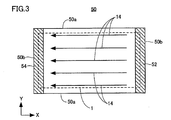
- FIG. 3 is a plan view of a planar conductor, a feeding electrode, and a termination electrode viewed from the matching circuit side shown in FIG. 2.
- 3 is a timing chart of gas flow rates in the insulating film manufacturing method 1 shown in FIG. 1.
- FIG. 1 It is a figure which shows the method of measuring the electrical property of the insulating film manufactured by the manufacturing method 1.
- FIG. It is a figure which shows the relationship between the dielectric breakdown electric field strength and leak current density, and gas flow ratio in the insulating film manufactured by the manufacturing method 1.
- FIG. FIG. 3 is a process diagram showing manufacturing method 1.
- FIG. 3 is a timing chart of gas flow rates in the insulating film manufacturing method 2 shown in FIG. 1. It is a figure which shows the relationship between the dielectric breakdown electric field strength and leakage current density, and gas flow ratio in the insulating film manufactured by the manufacturing method 2.
- FIG. FIG. 6 is a process diagram showing a manufacturing method 2. 4 is a timing chart of gas flow rates in the insulating film manufacturing method 3 shown in FIG. 1. 6 is a diagram illustrating a method of measuring electrical characteristics of an insulating film manufactured by a manufacturing method 3. FIG. It is a figure which shows the relationship between the leakage current in the insulating film manufactured by the manufacturing method 3, and gas flow ratio.
- FIG. 6 is a process diagram showing a manufacturing method 3.
- FIG. 5 is a schematic cross-sectional view of an example of a TFT according to Embodiments 2 to 4 of the present invention. It is a schematic enlarged view of the area
- FIG. 17 is a cross sectional view schematically showing a manufacturing step for the semiconductor element shown in FIG. 16. It is a schematic enlarged view of the area
- FIG. 1 is a cross-sectional view of an insulating film according to the first embodiment of the first invention.
- an insulating film 10 according to the first embodiment of the first invention includes a substrate 1, a silicon nitride film 2, and a silicon nitride film 3.
- the substrate 1 is made of a material containing O atoms such as glass and a-IGZO.
- the silicon nitride film 2 is disposed in contact with one main surface of the substrate 1.
- the silicon nitride film 3 is disposed in contact with the silicon nitride film 2.
- Each of the silicon nitride films 2 and 3 contains a fluorine atom and a hydrogen atom.
- Each of the silicon nitride films 2 and 3 has a hydrogen concentration of less than 5 atomic%.
- the fluorine concentration of the silicon nitride film 3 is higher than the fluorine concentration of the silicon nitride film 2.
- the silicon nitride film 2 has a thickness of, for example, 5 to 100 nm
- the silicon nitride film 3 has a thickness of, for example, 5 to 500 nm.
- FIG. 2 is a cross-sectional view showing the configuration of the plasma device according to Embodiment 1 of the present invention.
- the plasma apparatus 100 includes a vacuum vessel 20, a top plate 22, an exhaust port 24, a gas introduction unit 26, a holder 32, a heater 34, a shaft 36, a bearing unit 38, A mask 42, a partition plate 44, a planar conductor 50, a feeding electrode 52, a termination electrode 54, an insulating flange 56, packings 57 and 58, a shield box 60, a high frequency power supply 62, a matching circuit 64, Connection conductors 68 and 69 are provided.
- the vacuum vessel 20 is made of metal, and is connected to a vacuum exhaust device (not shown) through the exhaust port 24.
- the vacuum vessel 20 is electrically connected to the ground node.
- the top plate 22 is disposed in contact with the vacuum vessel 20 so as to close the upper side of the vacuum vessel 20.
- a vacuum seal packing 57 is disposed between the vacuum vessel 20 and the top plate 22.
- the gas introduction unit 26 is disposed above the partition plate 44 in the vacuum vessel 20.
- the shaft 36 is fixed to the bottom surface of the vacuum vessel 20 via a bearing portion 38.
- the holder 32 is fixed to one end of the shaft 36.
- the heater 34 is disposed in the holder 32.
- the mask 42 is disposed on the holder 32 at the peripheral edge of the holder 32.
- the partition plate 44 is fixed to the side wall of the vacuum vessel 20 so as to close the space between the vacuum vessel 20 and the holder 32 above the holder 32.
- the feeding electrode 52 and the termination electrode 54 are fixed to the top plate 22 via an insulating flange 56.
- a vacuum seal packing 58 is disposed between the top plate 22 and the insulating flange 56.
- the planar conductor 50 is disposed so that both end portions in the X direction are in contact with the feeding electrode 52 and the termination electrode 54, respectively.
- the feeding electrode 52 and the termination electrode 54 have substantially the same length as the planar conductor 50 in the Y direction (direction perpendicular to the paper surface of FIG. 2) as will be described later.
- the feeding electrode 52 is connected to the output bar 66 of the matching circuit 64 by the connection conductor 68.
- the termination electrode 54 is connected to the shield box 60 via the connection conductor 69.
- the planar conductor 50, the feeding electrode 52, and the termination electrode 54 are made of, for example, copper and aluminum.
- the shield box 60 is disposed on the upper side of the vacuum container 20 and contacts the top plate 22.
- the high frequency power supply 62 is connected between the matching circuit 64 and the ground node.
- the matching circuit 64 is disposed on the shield box 60.
- connection conductors 68 and 69 have a plate shape having substantially the same length as that of the feeding electrode 52 and the termination electrode 54 in the Y direction.
- the gas introduction unit 26 supplies a gas 28 such as SiF 4 gas, H 2 gas, and N 2 gas supplied from a gas cylinder (not shown) into the vacuum container 20.
- the holder 32 supports the substrate 1.
- the heater 34 heats the substrate 1 to a desired temperature.
- the shaft 36 supports the holder 32.
- the mask 42 covers the peripheral edge of the substrate 1. This can prevent the insulating film from being formed on the peripheral edge of the substrate 1.
- the partition plate 44 prevents the plasma 70 from reaching the holding mechanism of the substrate 1.
- the feeding electrode 52 allows the high-frequency current supplied from the connection conductor 68 to flow through the planar conductor 50.
- the termination electrode 54 connects the end of the planar conductor 50 to the ground node directly or via a capacitor, and forms a closed loop of a high-frequency current from the high-frequency power source 62 to the planar conductor 50.
- the high frequency power supply 62 supplies high frequency power of 13.56 MHz to the matching circuit 64, for example.
- the matching circuit 64 supplies the high-frequency power supplied from the high-frequency power source 62 to the connection conductor 68 while suppressing reflection.
- planar conductor 50 has, for example, a rectangular planar shape and has sides 50 a and 50 b.
- the side 50a is longer than the side 50b.
- the side 50a is disposed along the X direction, and the side 50b is disposed along the Y direction.
- the feeding electrode 52 and the termination electrode 54 are disposed at both ends of the planar conductor 50 in the X direction along the side 50b of the planar conductor 50, respectively.
- the lengths of the feed electrode 52 and the termination electrode 54 in the Y direction are close to the length of the side 50b parallel to the Y direction of the planar conductor 50 in order to flow the high-frequency current 14 as uniformly as possible in the Y direction (for example, It is preferable that the length is substantially the same as the length of the side 50b), but it may be slightly shorter or longer than the length of the side 50b.
- the lengths of the feeding electrode 52 and the termination electrode 54 in the Y direction may be set to 85% or more of the length of the side 50b.
- the power supply electrode 52 and the termination electrode 54 are formed of block-like electrodes, the high-frequency current 14 can flow through the planar conductor 50 almost uniformly in the Y direction.
- the plasma apparatus 100 generates inductively coupled plasma by causing the high-frequency current 14 to flow uniformly through the planar conductor 50.
- an insulating film is deposited on the substrate placed on the holder 32 by the inductively coupled plasma generated in the vacuum vessel 20.
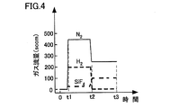
- FIG. 4 is a timing chart of the gas flow rate in the manufacturing method 1 of the insulating film 10 shown in FIG.
- silicon nitride film 2 is deposited on substrate 1 using SiF 4 gas, H 2 gas and N 2 gas, and then silicon is used using SiF 4 gas and N 2 gas.
- An insulating film 10 is manufactured by depositing the nitride film 3 on the silicon nitride film 2.
- the substrate 1 is made of patterned Mo / glass in which patterned molybdenum (Mo) is formed on glass. And the film thickness of Mo is 100 nm, and the thickness of glass is 0.5 mm. Moreover, the width
- the substrate temperature is 150 ° C.
- the pressure during film formation is 2.6 Pa
- the high frequency power is 1.1 W / cm 2 .
- the gas introduction unit 26 of the plasma apparatus 100 is configured to perform 25 sccm of SiF 4 gas, 450 sccm of N 2 gas, and 200 sccm of H 2 from timing t 1 to timing t 2. 2 gas is supplied to the vacuum vessel 20.
- the vacuum exhaust apparatus sets the pressure of the vacuum vessel 20 to 2.6 Pa.
- the heater 34 sets the temperature of the substrate 1 to 150 ° C.
- the high frequency power supply 62 supplies 1.1 W / cm 2 of high frequency power to the planar conductor 50 via the matching circuit 64, the connection conductor 68, and the feeding electrode 52.
- the gas introduction unit 26 increases the flow rate of the SiF 4 gas from 25 sccm to 100 sccm, decreases the flow rate of the N 2 gas from 450 sccm to 250 sccm, and stops the H 2 gas. Thereafter, the gas inlet 26 supplies 100 sccm of SiF 4 gas and 250 sccm of N 2 gas to the vacuum container 20 until timing t3.
- a silicon nitride film 3 having a thickness of 200 nm is deposited on the silicon nitride film 2.
- the gas introduction unit 26 stops the SiF 4 gas and the N 2 gas at timing t3.
- the high-frequency power, the reaction pressure, and the substrate temperature are set to the above-described values.
- the film is formed by adding H 2 gas to the gas, and the silicon nitride film 3 is formed without adding H 2 gas to the SiF 4 gas.
- the fluorine concentration of the silicon nitride film 3 is higher than the fluorine concentration of the silicon nitride film 2.
- FIG. 5 is a diagram illustrating a method of measuring the electrical characteristics of the insulating film manufactured by the manufacturing method 1.
- a silicon nitride film is deposited on the patterned Mo / glass by manufacturing method 1. Then, an electrode is formed on the surface of the silicon nitride film.
- the power supply applies a voltage in the thickness direction of the silicon nitride film while changing the voltage value. And an ammeter measures the leakage current which flows into a silicon nitride film. Further, a value obtained by dividing the voltage value applied by the power source by the film thickness of the silicon nitride film is defined as a dielectric breakdown electric field strength.
- FIG. 6 is a diagram showing the relationship between the dielectric breakdown electric field strength, the leakage current density, and the gas flow rate ratio in the insulating film manufactured by the manufacturing method 1.
- the vertical axis represents the breakdown field strength and the leakage current density
- the horizontal axis represents the ratio of the flow rate of H 2 gas to the flow rate of SiF 4 gas.
- a curve k1 shows the relationship between the dielectric breakdown electric field strength and the gas flow rate ratio
- a curve k2 shows the relationship between the leakage current density and the gas flow rate ratio.
- the dielectric breakdown electric field strength is about 5 [MV / cm]
- the leakage current density is about 1 ⁇ 10 ⁇ 6 [A / cm 2 ].
- the silicon nitride film 2 may be formed using ammonia (NH 3 ) gas instead of H 2 gas, and generally silicon using a gas containing H atoms.
- NH 3 ammonia
- the nitride film 2 may be formed.
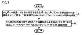
- FIG. 7 is a process diagram showing the manufacturing method 1. Referring to FIG. 7, when the production of insulating film 10 is started, the ratio of the total flow rate of the gas containing hydrogen atoms and the flow rate of N 2 gas to the flow rate of SiF 4 gas is set to a reference value or more to include oxygen atoms. A silicon nitride film 2 is formed on the substrate (step S1).
- the ratio of the flow rate of N 2 gas to the flow rate of SiF 4 gas is set to a value smaller than the reference value, and the silicon nitride film 3 is formed on the silicon nitride film 2 (step S2).
- FIG. 8 is a timing chart of the gas flow rate in the manufacturing method 2 of the insulating film 10 shown in FIG.
- a silicon nitride film 2 by using SiF 4 gas and N 2 gas , 3 are sequentially deposited on the substrate 1 to manufacture the insulating film 10.
- the substrate 1 is Mo / glass in which Mo is formed on glass. And the film thickness of Mo is 100 nm, and the thickness of glass is 0.5 mm.
- the substrate temperature is 150 ° C.
- the pressure during film formation is 2.6 Pa
- the high frequency power is 1.1 W / cm 2 .
- gas introduction unit 26 of plasma apparatus 100 supplies 500 sccm of N 2 gas to vacuum container 20 from timing t 4 to timing t 5. To do.
- the vacuum exhaust apparatus sets the pressure in the vacuum vessel 20 to 2.6 Pa.
- the heater 34 sets the temperature of the substrate 1 to 150 ° C.
- the high frequency power supply 62 supplies 1.1 W / cm 2 of high frequency power to the planar conductor 50 via the matching circuit 64, the connection conductor 68, and the feeding electrode 52.
- the gas introduction unit 26 supplies 25 sccm of SiF 4 gas and 450 sccm of N 2 gas to the vacuum container 20 from timing t5 to timing t6.
- a silicon nitride film 2 having a thickness of 10 nm is deposited on the substrate 1.
- the gas introduction unit 26 increases the flow rate of the SiF 4 gas from 25 sccm to 100 sccm, and decreases the flow rate of the N 2 gas from 450 sccm to 250 sccm. Thereafter, the gas inlet 26 supplies 100 sccm of SiF 4 gas and 250 sccm of N 2 gas to the vacuum container 20 until timing t7.
- a silicon nitride film 3 having a thickness of 90 nm is deposited on the silicon nitride film 2.
- the gas introduction unit 26 stops the SiF 4 gas and the N 2 gas at timing t7.
- the high-frequency power, the reaction pressure, and the substrate temperature are set to the values described above.
- the silicon nitride films 2 and 3 are formed by changing the ratio of the flow rate of N 2 gas to the flow rate of SiF 4 gas.
- the insulating film 10 manufactured by the manufacturing method 2 applies a voltage to the insulating film 10 from the film thickness direction of the insulating film 10 in the same manner as the insulating film 10 manufactured by the manufacturing method 1, thereby causing a breakdown electric field strength. And the leakage current density was measured.
- FIG. 9 is a diagram showing the relationship between the dielectric breakdown electric field strength, the leakage current density, and the gas flow rate ratio in the insulating film manufactured by the manufacturing method 2.
- the vertical axis represents the breakdown field strength and the leakage current density
- the horizontal axis represents the ratio of the flow rate of N 2 gas to the flow rate of SiF 4 gas.
- a curve k3 shows the relationship between the breakdown electric field strength and the gas flow rate ratio
- a curve k4 shows the relationship between the leakage current density and the gas flow rate ratio.
- an insulating film (silicon nitride film 2 / silicon nitride film 3) having good insulating performance can be manufactured. This is because the substrate 1 in which the glass is covered with Mo is used, so that oxygen atoms are not extracted from the glass by F radicals in the plasma, and oxygen atoms are not easily taken into the silicon nitride films 2 and 3. It is.
- the number of F radicals in the plasma is larger when the silicon nitride film 3 is formed than when the silicon nitride film 2 is formed. Therefore, the fluorine concentration of the silicon nitride film 3 is higher than the fluorine concentration of the silicon nitride film 2.
- the insulating film 10 manufactured by the manufacturing method 2 has good insulating performance.
- the plasma treatment using N 2 gas may be omitted.
- FIG. 10 is a process diagram showing the manufacturing method 2.
- the ratio of the flow rate of N 2 gas to the flow rate of SiF 4 gas is set to a reference value or more, and a silicon nitride film is formed on the substrate containing oxygen atoms. 2 is formed (step S11).
- the ratio of the N 2 gas flow rate to the SiF 4 gas flow rate is set to a value smaller than the reference value, and the silicon nitride film 3 is formed on the silicon nitride film 2 (step S12).
- FIG. 11 is a timing chart of the gas flow rate in the manufacturing method 3 of the insulating film 10 shown in FIG.
- the silicon nitride film 2 is deposited on the substrate 1 using SiF 4 gas, a gas containing oxygen atoms or hydrogen atoms, and N 2 gas, and then SiF 4 gas and N 2 are used.
- the insulating film 10 is manufactured by depositing the silicon nitride film 3 on the silicon nitride film 2 using a gas.
- the substrate 1 is an IGZO / SiN x / silicon wafer in which SiN x and a-IGZO are sequentially deposited on a silicon wafer.
- the film thickness of a-IGZO is 100 nm
- the film thickness of SiN x is 100 nm
- the thickness of the silicon wafer is 0.55 mm.
- the substrate temperature is 150 ° C.
- the pressure during film formation is 2.6 Pa
- the high frequency power is 1.1 W / cm 2 .
- the gas introduction unit 26 of the plasma apparatus 100 is configured to perform 25 sccm SiF 4 gas, 450 sccm N 2 gas, and 100 sccm N 2 from timing t1 to timing t2. 2 O gas is supplied to the vacuum vessel 20.
- the vacuum exhaust apparatus sets the pressure in the vacuum vessel 20 to 2.6 Pa.
- the heater 34 sets the temperature of the substrate 1 to 150 ° C.
- the high frequency power supply 62 supplies 1.1 W / cm 2 of high frequency power to the planar conductor 50 via the matching circuit 64, the connection conductor 68, and the feeding electrode 52.
- the gas introduction unit 26 increases the flow rate of the SiF 4 gas from 25 sccm to 100 sccm, decreases the flow rate of the N 2 gas from 450 sccm to 250 sccm, and stops the N 2 O gas. Thereafter, the gas inlet 26 supplies 100 sccm of SiF 4 gas and 250 sccm of N 2 gas to the vacuum container 20 until timing t3.
- a silicon nitride film 3 having a thickness of 50 nm is deposited on the silicon nitride film 2.
- the gas introduction unit 26 stops the SiF 4 gas and the N 2 gas at timing t3.
- the high-frequency power, the reaction pressure, and the substrate temperature are set to the above-described values.
- the film is formed by adding N 2 O gas to SiF 4 gas, and the silicon nitride film 3 is formed without adding N 2 O gas to SiF 4 gas.
- the fluorine concentration of the silicon nitride film 3 is higher than the fluorine concentration of the silicon nitride film 2.
- FIG. 12 is a diagram showing a method of measuring the electrical characteristics of the insulating film manufactured by the manufacturing method 3.
- a silicon nitride film is deposited on a-IGZO of an IGZO / SiN x / silicon wafer by manufacturing method 3.
- a power source and an ammeter are connected in series between two different points of the a-IGZO.
- the power supply applies a voltage between two different points of a-IGZO while changing the voltage value.
- the ammeter then measures the leak current flowing on the surface of the a-IGZO.
- FIG. 13 is a diagram showing the relationship between the leakage current and the gas flow rate ratio in the insulating film manufactured by the manufacturing method 3.
- the vertical axis represents the leakage current
- the horizontal axis represents the ratio of the flow rate of N 2 O gas to the flow rate of SiF 4 gas.
- a curve k5 shows the relationship between the leakage current and the gas flow rate ratio.
- the silicon nitride film 2 may be formed using any one of oxygen (O 2 ) gas, H 2 gas and NH 3 gas instead of N 2 O gas.
- the silicon nitride film 2 may be formed using a gas containing hydrogen atoms or oxygen atoms.
- FIG. 14 is a process diagram showing the manufacturing method 3.
- the ratio of the total flow rate of the gas containing hydrogen atoms or oxygen atoms and the flow rate of N 2 gas to the flow rate of SiF 4 gas is set to a reference value or more to set oxygen.
- a silicon nitride film 2 is formed on the substrate containing atoms (step S21).
- the ratio of the flow rate of N 2 gas to the flow rate of SiF 4 gas is set to a value smaller than the reference value, and the silicon nitride film 3 is formed on the silicon nitride film 2 (step S22).
- SiF 4 gas is used as the main gas for forming the silicon nitride films 2 and 3.
- the main gas for forming the ride films 2 and 3 may be a gas containing fluorine atoms and silicon atoms.
- SiF 4 gas is used as the main gas
- a gas containing hydrogen atoms and N 2 gas are used as the sub gas
- the ratio of the flow rate of the sub gas to the flow rate of the main gas is set to a reference value or more.
- the silicon nitride film 2 is formed, SiF 4 gas is used as the main gas, N 2 gas is used as the sub gas, and the ratio of the flow rate of the sub gas to the flow rate of the main gas is set to a value smaller than the reference value.
- a silicon nitride film 3 was formed.
- the ratio of the flow rate of the secondary gas to the flow rate of the primary gas is set to a reference value or higher using SiF 4 gas as the primary gas and N 2 gas as the secondary gas.
- the ratio of the flow rate of the secondary gas to the flow rate of the main gas is set to a value smaller than the reference value by using SiF 4 gas as the main gas and N 2 gas as the secondary gas.
- the ratio of the flow rate of the secondary gas to the flow rate of the primary gas is greater than the reference value using the SiF 4 gas as the primary gas and the gas containing hydrogen atoms or oxygen atoms and the N 2 gas as the secondary gas.
- the silicon nitride film 2 is formed with the SiF 4 gas as the main gas and the N 2 gas as the sub gas, and the ratio of the flow rate of the sub gas to the flow rate of the main gas is smaller than the reference value. Then, a silicon nitride film 3 was formed.
- the manufacturing method of the insulating film 10 according to the embodiment of the first invention may be the manufacturing method shown in FIG.
- FIG. 15 is a process diagram showing a method of manufacturing the insulating film 10 according to the embodiment of the first invention.
- the gas flow rate ratio between the main gas containing silicon atoms and fluorine atoms and the sub-gas consisting of at least nitrogen gas is set to a reference value or more.
- a first silicon nitride film is formed on the substrate containing oxygen atoms (step S31).
- a gas flow ratio between the main gas and nitrogen gas is set to a value smaller than the reference value, and a second silicon nitride film is formed in contact with the first silicon nitride film (step S32).
- the insulating film 10 manufactured by the manufacturing methods 1 to 3 described above has a structure in which the fluorine concentration of the silicon nitride film 3 is higher than the fluorine concentration of the silicon nitride film 2. That is, the fluorine concentration of the silicon nitride film 2 is lower than the fluorine concentration of the silicon nitride film 3. As described above, this is because the concentration of F radicals in the plasma during the formation of the silicon nitride film 2 is made lower than the concentration of F radicals in the plasma during the formation of the silicon nitride film 3. This is due to the formation of the ride film 2.
- the fluorine concentration in the silicon nitride film on the substrate 1 side is lower than the fluorine concentration in the silicon nitride film on the surface side of the insulating film 10, oxygen atoms are insulated. Mixing into the film 10 is reduced, and good insulation performance can be obtained.
- Embodiments 2 to 4 ⁇ Embodiments 2 to 4>
- semiconductor elements of Embodiments 2 to 4 which are embodiments of the second invention of the present invention, will be described.
- the same or corresponding parts are denoted by the same reference numerals, and description thereof will not be repeated.
- the semiconductor element of the second invention includes an oxide semiconductor layer containing at least indium (In) atoms and oxygen (O) atoms, and an insulation containing silicon (Si) atoms, fluorine (F) atoms, and nitrogen (N) atoms. And a membrane.
- the present inventors have found that a change in Vth can be suppressed when a semiconductor element made of a TFT has the oxide semiconductor layer and the insulating film in contact with the oxide semiconductor layer. Although the reason is not clear, for example, the following is considered as one of the reasons.
- the O content, the H content, the N content, and their chemical bonding state in the layer affect the semiconductor characteristics.
- the oxide semiconductor layer in contact with the oxide semiconductor layer contains Si, F, and N
- the oxide semiconductor layer has little influence on the content, chemical bonding state, and the like of O, H, and N in the oxide semiconductor layer.
- the influence on the semiconductor characteristics of the oxide semiconductor layer due to the presence of the layer in contact with the layer can be suppressed, and as a result, the change in Vth of the TFT can be suppressed.
- the present inventors have found that it is important that F is present in the insulating film by conducting various studies.
- FIG. 16 is a schematic cross-sectional view of an example of a semiconductor element.
- a gate electrode 202, a gate insulating film 203, and a semiconductor layer 204 as a channel layer are sequentially stacked on a substrate 201.
- a source electrode 205 and a semiconductor layer 204 are stacked on the semiconductor layer 204.
- a drain electrode 206 is stacked.
- a passivation film 207 is stacked in a region of the semiconductor layer 204 that is between the source electrode 205 and the drain electrode 206 and is not covered with both electrodes.
- the TFT in FIG. 16 is a so-called bottom-gate transistor, and can be suitably used as a switching element in a liquid crystal display device, for example.
- an insulating substrate such as a plastic film or a glass substrate can be used.
- a metal such as Ti, Mo, or Al can be used.
- the passivation film 207 may be an insulating film made of silicon (Si) atoms, fluorine (F) atoms, and nitrogen (N) atoms.
- silicon oxide (SiO 2 ), silicon nitride (SiN), yttrium oxide A film made of (Y 2 O 3 ), aluminum oxide (Al 2 O 3 ), hafnium oxide (Hf 2 O 2 ), titanium oxide (TiO 2 ), or the like can also be used.
- the change in Vth of the semiconductor element can be suppressed by making the composition of the semiconductor layer 204 and the composition of the gate insulating film 203 characteristic.
- the semiconductor layer 204 and the gate insulating film 203 will be described in detail.
- the semiconductor layer 204 is formed of an oxide semiconductor layer containing In and O. Specifically, the semiconductor layer 204 is preferably made of any one of In—Ga—Zn—O, In—Al—Mg—O, In—Al—Zn—O, and In—Hf—Zn—O. Note that the description of “In—Ga—Zn—O” means an oxide semiconductor containing In, Ga, Zn, and O as its main components, and contains a small amount of other unintended atoms to the extent that the semiconductor characteristics do not change. Including those that are.
- the ratio of the In content to the total amount of In, Ga, and Zn contained in the semiconductor layer 204 is 35 atoms.
- the change in Vth can be suppressed.
- the change in Vth can be further suppressed by setting the ratio of the In content to 38 atomic% or more and 43 atomic% or less.
- the content of O in the semiconductor layer 204 is preferably 60 atomic% or more and 66 atomic% or less. Note that Rutherford backscattering, ICP mass spectrometry, or the like can be used as a method for quantifying each element in the semiconductor layer 204.
- the concentration of the additive element in the semiconductor layer 204 is preferably 0.1 ⁇ 10 21 atm / cc or more and 10 ⁇ 10 21 atm / cc or less.
- concentration (atm / cc) of the additive element in the semiconductor layer 204 can be measured by, for example, a secondary ion mass spectrometry (SIMS) method.
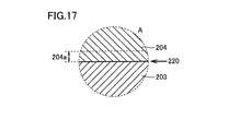
- the ratio A / B of the oxygen amount A in the semiconductor layer 204 in the vicinity of the interface where the semiconductor layer 204 and the gate insulating film 203 described later are in contact with the oxygen amount B in the semiconductor layer 204 other than in the vicinity of the interface is more than 0.78 It is preferably large and less than 1. This will be described with reference to FIG.
- FIG. 17 is a schematic enlarged view of region A in FIG. Referring to FIG. 17, in the second embodiment, in the semiconductor layer 204, the oxygen amount A of the semiconductor layer 204 located in the region 204a in the vicinity of the interface 220 in contact with the gate insulating film 203, and other than the vicinity of the interface
- the ratio A / B of the semiconductor layer that is, the oxygen amount B of the semiconductor layer 204 located in a portion other than the region 204a is preferably greater than 0.78 and less than 1. In this case, the ON current flowing between the source and drain of the TFT can be increased.
- the ratio A / B is 0.78, the OFF current flowing between the source and the drain tends to become excessively large. Therefore, from the viewpoint of stabilizing the TFT characteristics under more appropriate conditions, the ratio A / B is preferably 0.8 or more and less than 1, and more preferably 0.8 or more and 0.98 or less. preferable.
- the “interface in contact” means that, in secondary ion mass spectrometry, the ion count number of ions caused by F in the gate insulating film 203 and the ion count number of ions caused by In in the semiconductor layer 204 intersect.
- the term “near the interface” means a region 204a having a thickness of 0.1 nm to 20 nm from the “interface in contact”.
- the oxygen amount A and the oxygen amount B are the count numbers of oxygen ions by secondary ion mass spectrometry at arbitrary positions of the semiconductor layer 204, respectively.
- the ratio A / B of the oxygen amount A and the oxygen amount B in at least a part of the region 204a is in the above range, the above effect can be exhibited. That is, for example, the ratio A / B between the oxygen amount A and the oxygen amount B in the region from 0.1 nm to 5 nm from the interface 220 in the region 204a of the semiconductor layer 204 may be in the above range. Further, it is sufficient that the ratio A / B is satisfied in at least a part of the region 204a in the vicinity of the interface. That is, referring to FIG. 17, the oxygen amount A and the oxygen amount B in at least a part of the region 204a extending in the horizontal direction in the drawing (for example, the central portion of the region 204a) are within the range of the ratio A / B. Should be satisfied.
- the gate insulating film 203 includes Si, F, and N.
- the semiconductor layer 204 is made of an oxide semiconductor layer containing In and O, and the gate insulating film 203 contains Si, F, and N, whereby change in Vth can be suppressed.
- SEM scanning secondary electron microscope
- TEM transmission electron microscope
- An optical X-ray analysis (EDX) method or the like can be used.
- other known techniques used for qualitative analysis of elements may be used.
- the content of F in the gate insulating film 203 is preferably greater than 0 atomic% and 30 atomic% or less. Further, the content of F is more preferably 3 atomic% or more, and further preferably 5 atomic% or more. In particular, when the F content is 10 atomic% or more and 28 atomic% or less, the amount of change in Vth can be reduced more efficiently.
- the Si content is preferably 25 atomic percent or more and 35 atomic percent or less, and the N content is preferably 25 atomic percent or more and 40 atomic percent or less.
- the gate insulating film 203 may further contain H. Since the gate insulating film 203 contains H, an effect of increasing Ion (on-current) is expected. Since the amount of change in Vth tends to increase when the H content in the gate insulating film 203 exceeds 7 atomic%, the H content is preferably 7 atomic% or less. Further, it is more preferably 5 atomic% or less from the viewpoint of further suppressing the change in Vth characteristics.
- a method for quantifying H in the gate insulating film 203 for example, secondary ion mass spectrometry can be used.
- H in the measurement sample can be quantified.
- the H content can also be quantified by using both Rutherford backscattering method and elastic recoil detection method.
- the gate insulating film 203 may further contain O. Since the gate insulating film 203 contains O, an effect of increasing Ion is expected. Since the change in Vth tends to increase when the O content in the gate insulating film 203 is 25 atomic% or more, the O content is preferably less than 25 atomic%, and is 20 atomic% or less. It is more preferable.
- a method for quantifying O atoms in the gate insulating film 203 Rutherford backscattering method, secondary ion mass spectrometry, or the like can be used.
- a substrate 201 made of a glass substrate is prepared, and a gate electrode 202 is formed on the surface 201a of the substrate 201 by, for example, DC sputtering.
- a gate insulating film 203 is formed so as to cover the surface 201 a of the substrate 201 and the gate electrode 202.
- the gate insulating film 203 contains Si, F, and N.
- a plasma CVD method can be used as a method for forming such a gate insulating film 203.
- a plasma CVD method using an internal antenna type ICP plasma source can be suitably used.
- the substrate 201 on which the gate electrode 202 is formed is set in the vacuum chamber of the plasma apparatus, and after evacuating the vacuum chamber, the source gas such as SiF 4 and N 2 is placed in the vacuum chamber. Is introduced. Then, by activating the source gas using a plasma source, the gate insulating film 203 containing Si, F, and N can be formed.
- the contents of Si, F, and N in the gate insulating film 203 can be adjusted. Further, by mixing a gas containing H, for example, H 2 gas, into the source gas, the gate insulating film 203 can contain H, and a gas containing O, for example, O 2 gas, is mixed into the source gas. Accordingly, O can be contained in the gate insulating film 203.
- a gas containing H for example, H 2 gas
- a semiconductor layer 204 as a channel layer is formed in a part on the gate insulating film 203.
- the semiconductor layer 204 contains In and O.
- a DC (direct current) magnetron sputtering method can be used as a method for forming such a semiconductor layer 204.
- a target made of a conductive oxide sintered body that is a raw material for an oxide semiconductor is prepared as a target.
- the semiconductor layer 204 including In—Ga—Zn—O is formed, it is preferable to use a target including a ZnGa 2 O 4 crystal in that the amount of change in Vth can be further reduced.
- the target and the substrate 201 are placed at predetermined positions in the apparatus, and the target is sputtered by a DC magnetron sputtering method to form a semiconductor layer on the gate insulating film 203.
- a resist having a predetermined shape is formed by applying a resist on the semiconductor layer, exposing and developing so that the obtained semiconductor layer has a predetermined channel width and channel length. Then, the substrate 201 on which a resist having a predetermined shape is formed is immersed in an etching aqueous solution, and the exposed semiconductor layer is etched to be laminated on a part of the gate insulating film 203 as shown in FIG. The semiconductor layer 204 to be formed is formed.
- the semiconductor layer 204 further includes N as an additive element, for example, N 2 gas is mixed into the gas introduced into the sputtering apparatus when sputtering the target, and the mixing ratio is controlled.
- N 2 gas is mixed into the gas introduced into the sputtering apparatus when sputtering the target, and the mixing ratio is controlled.
- the concentration of N in the semiconductor layer 204 can be adjusted.
- the semiconductor layer 204 when adjusting the ratio A / B of the oxygen amount A in at least a part of the region 204a and the oxygen amount B in a region other than the region 204a in the semiconductor layer 204, the semiconductor layer 204 the mixing ratio of O 2 gas introduced into the sputtering apparatus for forming the portion of the interface 220 near the region 204a of the 204 may be adjusted.
- the source electrode 205 and the drain electrode 206 are formed on the semiconductor layer 204 and the gate insulating film 203 by, for example, DC sputtering.
- a resist is applied, exposed, and developed on the semiconductor layer 204, and then the source electrode 205 made of a metal layer is formed on the semiconductor layer 204 on which the resist is not formed and the gate insulating film 203 by a DC sputtering method. And a drain electrode 206 are formed. Then, by removing the resist on the semiconductor layer 204, the substrate 201 on which the source electrode 205 and the drain electrode 206 are formed is formed as shown in FIG.
- a passivation film 207 is formed on the semiconductor layer 204 exposed from the source electrode 205 and the drain electrode 206.
- a DC magnetron sputtering method can be used for the formation of the passivation film 207.
- the semiconductor layer 204 is made of an oxide semiconductor layer containing In and O
- the gate insulating film 203 is made of an insulating film containing Si, F, and N. According to the TFT having this configuration, it is possible to suppress a change in Vth when the gate-source voltage or the source-drain voltage is used at ⁇ 20 V or more. Therefore, as a result, the characteristics of the TFT can be stabilized.
- the TFT of the third embodiment has a configuration shown in FIG.
- the configuration other than the semiconductor layer 204, the gate insulating film 203, and the passivation film 207 is the same as that of the second embodiment, and thus description thereof is not repeated.
- the gate insulating film 203 may be an insulating film containing Si, F, and N.
- silicon oxide (SiOH), silicon nitride (SiNH), yttrium oxide (Y A conventionally used insulating film made of 2 O 3 ), aluminum oxide (Al 2 O 3 ), hafnium oxide (Hf 2 O 2 ), titanium oxide (TiO 2 ), or the like can be used.
- the semiconductor layer 204 and the passivation film 207 will be described in detail.
- the semiconductor layer 204 is formed of an oxide semiconductor layer containing In and O. Specifically, the semiconductor layer 204 is preferably made of any one of In—Ga—Zn—O, In—Al—Mg—O, In—Al—Zn—O, and In—Hf—Zn—O.
- the ratio C / D of the oxygen amount C in the semiconductor layer 204 in the vicinity of the interface where the semiconductor layer 204 and a passivation film 207 to be described later are in contact with the oxygen amount D in the semiconductor layer 204 other than in the vicinity of the interface is 1.05 or more. It is preferable that it is 3 or less. This will be described with reference to FIG.
- FIG. 19 is a schematic enlarged view of region B in FIG.
- the amount of oxygen C in the semiconductor layer 204 located in the region 204b in the vicinity of the interface 240 in contact with the passivation film 207 and the semiconductor other than in the vicinity of the interface It is preferable that the ratio C / D with respect to the oxygen amount D of the semiconductor layer 204 located in a layer other than the region 204b is 1.05 or more. In this case, the OFF current flowing between the source and drain of the TFT can be reduced. On the other hand, when the ratio C / D exceeds 1.3, the ON current flowing between the source and the drain tends to be too low. Therefore, the ratio C / D is preferably 1.3 or less.
- the “interface in contact” intersects the ion count number of ions caused by F in the passivation film 207 and the ion count number of ions caused by In in the semiconductor layer 204.
- the “near interface” means a region 204b having a thickness of 0.1 nm or more and 20 nm or less from the “contacting interface”.
- the oxygen amount C and the oxygen amount D are the count numbers of oxygen ions by secondary ion mass spectrometry at arbitrary positions of the semiconductor layer 204, respectively.
- the ratio C / D of the oxygen amount C and the oxygen amount D in at least a part of the region 204b is in the above range, the above effect can be exhibited, and the region 204b in the vicinity of the interface As in the second embodiment, it is sufficient that the ratio C / D is satisfied at least in part.
- the passivation film 207 includes Si, F, and N.
- the semiconductor layer 204 is made of an oxide semiconductor layer containing In and O, and the passivation film 207 contains Si, F, and N, whereby the change in Vth can be suppressed.
- the composition of the passivation film 207 is the same as the composition of the gate insulating film 203 in the second embodiment. That is, the F content in the passivation film 207 is preferably greater than 0 atomic percent and not greater than 30 atomic percent, more preferably 3 atomic percent or greater, and more preferably 5 atomic percent or greater. Is more preferable. In particular, when the F content is 10 atomic% or more and 28 atomic% or less, the amount of change in Vth can be reduced more efficiently. Further, when the passivation film 207 further contains H, the H content is preferably 7 atomic% or less, and more preferably 5 atomic% or less. Further, when the passivation film 207 further contains O, the content of O is preferably less than 25 atomic%, and more preferably 15 atomic% or less.
- ⁇ Semiconductor element manufacturing method ⁇ As a manufacturing method of the TFT according to the third embodiment, the same method as the manufacturing method of the second embodiment can be used. Specifically, in the formation of the passivation film 207 in the third embodiment, the method for forming the gate insulating film 203 in the second embodiment can be used. Note that the gate insulating film 203 in Embodiment 3 can be formed by a conventionally used method.
- the method for forming the semiconductor layer 204 in Embodiment 2 can be used.
- the amount of oxygen in the sputtering apparatus when the semiconductor layer 204 is formed in the vicinity of the interface in contact with the passivation film 207 is controlled. It is necessary to form the semiconductor layer 204 that satisfies C / D.
- the semiconductor layer is made of an oxide semiconductor layer containing In and O
- the passivation film is made of an insulating film containing Si, F and N.
- the TFT of the fourth embodiment has a configuration shown in FIG.
- the semiconductor layer 204 is formed of an oxide semiconductor layer containing In and O, and any of the gate insulating film 203 and the passivation film 207 contains Si, F, and N. That is, in the fourth embodiment, the gate insulating film 203 has the same composition as the gate insulating film 203 in the second embodiment, and the passivation film 207 has the same composition as the passivation film 207 in the third embodiment.
- the change in Vth when the gate-source or source-drain voltage is used at ⁇ 20 V or more can be suppressed. Therefore, as a result, the characteristics of the TFT can be stabilized.
- the semiconductor layer 204 in at least one of a region 204a (see FIG. 17) in the vicinity of the interface in contact with the gate insulating film 203 and a region 204b (see FIG. 18) in the vicinity of the interface in contact with the passivation film 207, By satisfying the ratios (A / B and C / D) described in detail in Embodiments 2 and 3, the OFF current and / or the ON current can be designed to an appropriate numerical value. The characteristics can be further stabilized.
- bottom gate type TFTs shown in FIG. 16 were fabricated.
- a substrate 201 made of an alkali-free glass of 25 mm ⁇ 25 mm ⁇ 0.5 mm was prepared.
- a target made of Al and a target made of Mo were prepared as raw materials for the gate electrode.
- Each target was processed so as to have a diameter of 3 inches (76.2 mm) and a thickness of 5.0 mm.
- Each target was placed in a target holder in the sputtering apparatus so that the surface of each target having a diameter of 3 inches was a sputtering surface, and the substrate was placed in the substrate holder in the sputtering apparatus. At this time, the distance between the target and the substrate was 100 mm.
- the inside of the sputtering apparatus is evacuated to about 1 ⁇ 10 ⁇ 4 Pa, and with the shutter placed between the substrate and the target, Ar gas is introduced into the apparatus to reduce the pressure in the apparatus to 0.5 Pa. Furthermore, the surface of each target was cleaned (pre-sputtering) for 10 minutes by applying a 150 W DC power to the target and performing sputtering discharge.
- DC sputtering was performed in the order of the target made of Mo, the target made of Al, and the target made of Mo to form a metal layer having a three-layer structure of Mo layer / Al layer / Mo layer on the surface of the substrate.
- the film thickness of each Mo layer was 20 nm, and the film thickness of the gate electrode having a three-layer structure was 100 nm.
- the gate electrode which has a desired wiring pattern was created by performing dry etching.
- a gate insulating film was formed on the exposed surface of the substrate and the surface of the gate electrode.
- a substrate on which a gate electrode was formed was placed in a vacuum chamber of a plasma apparatus, and evacuation was performed until the pressure in the vacuum chamber became 10 ⁇ 5 Pa or less.
- SiF 4 and N 2 were introduced into the vacuum chamber as source gases, and the pressure in the vacuum chamber was set to 0.5 Pa.
- a gate insulating film made of Si, F and N was formed.
- Examples 2 to 4 a gate insulating film made of Si, F, N, and H was formed by introducing H 2 gas in addition to SiF 4 and N 2 as source gases.
- a gate insulating film made of Si, F, N, H, and O was formed by introducing H 2 gas and O 2 gas in addition to SiF 4 and N 2 as source gases.
- F is a ratio of SiF 4 and N 2 (SiF 4 / N 2 ) in the source gas, which is 1/1 to 1
- the content in the gate insulating film of each example was adjusted.
- the content of O in the gate insulating film of each example is adjusted by adjusting the ratio of O 2 to N 2 (O 2 / N 2 ) in the source gas in the range of 0 to 1/10.
- H is contained in the gate insulating film of each embodiment by adjusting the ratio of H 2 to N 2 in the source gas (H 2 / N 2 ) in the range of 0 to 1/50. The amount was adjusted.
- a semiconductor layer was formed on the gate insulating film.
- a conductive oxide sintered body serving as a raw material for each semiconductor layer was prepared as a target.
- the target was processed so as to have a shape with a diameter of 3 inches (76.2 mm) and a thickness of 5.0 mm.
- the target was placed on the target holder in the sputtering apparatus so that the 3 inch diameter surface of the target became the sputtering surface, and the substrate on which the gate insulating film was formed was placed on the water-cooled substrate holder in the sputtering apparatus. At this time, the distance between the target and the substrate was 40 mm.
- the inside of the sputtering apparatus is evacuated to about 1 ⁇ 10 ⁇ 4 Pa, and with the shutter placed between the substrate and the target, Ar gas is introduced into the apparatus so that the pressure in the apparatus is 1 Pa. Further, the surface of each target was cleaned (pre-sputtering) for 10 minutes by applying a 120 W DC power to the target and performing sputtering discharge.
- a mixed gas having a ratio of the Ar gas volume to the O 2 gas volume of 93 (Ar): 7 (O 2 ) is introduced into the apparatus so that the pressure in the apparatus is 0.8 Pa, and 120 W is applied to the target.
- a semiconductor layer made of an oxide semiconductor layer having a thickness of 70 nm was formed on the gate insulating film by applying the sputtering DC power.
- the substrate holder was only cooled with water, and no bias voltage was applied.
- the conductive oxide sintered body used as a target was a polycrystalline body.
- ZnGa 2 O 4 crystals The phase was included in part.
- the shape shown in FIG. The channel width was 20 ⁇ m and the channel length was 10 ⁇ m.
- the semiconductor layer which consists of a structural element shown in Table 1 in each Example was formed.
- ⁇ Formation of source electrode and drain electrode >> Next, after the annealing treatment, a resist is applied to the semiconductor layer and the gate insulating film so that only portions of the semiconductor layer and the gate insulating film where the source electrode and the drain electrode are formed are exposed and exposed. Developed. Next, by forming a metal layer made of Mo, a metal layer made of Al, and a metal layer made of Mo in this order on the part where the resist is not formed (electrode forming part) using a sputtering method, Mo A source electrode and a drain electrode having a three-layer structure of layer / Al layer / Mo layer were formed. The film thickness of each three-layer structure was 100 nm. Thereafter, the resist was peeled off. The substrate was annealed in nitrogen at 150 ° C. for 1 hour.
- a passivation film was formed on the exposed semiconductor layer.
- the method for forming the passivation film in Examples 1 to 10 was the same as the method for forming the gate insulating film in each Example. Therefore, in each of Examples 1 to 10, the composition of the gate insulating film and the composition of the passivation film were the same.
- the thickness of the passivation film in each example was 500 nm. Then, after forming a passivation film, this structure was annealed in a nitrogen atmosphere at 150 ° C. for 2 hours to complete a TFT.
- a gate insulating film made of Si, F, N, H and O was formed by introducing H 2 gas and O 2 gas in addition to SiF 4 and N 2 as source gases.
- the ratio of the volume of Ar gas to the volume of O 2 gas is 90 (Ar): 10 ( It was controlled in the range of O 2 ) to 70:30.
- the oxygen ion count number C in the secondary ion mass spectrometry in the vicinity of the interface in the semiconductor layer at a predetermined position, and the interface The ratio C / D of the count number D of oxygen ions in secondary ion mass spectrometry in the semiconductor layer other than the vicinity was 1.05 to 1.35.
- the thickness of the semiconductor layer that becomes the “semiconductor layer in the vicinity of the interface” in each of Examples 11 to 16 is shown as “the thickness of the interface layer” in Table 1.
- a ZnGa 2 O 4 crystal phase was used. It was included in some.
- TFTs were produced in each example using the same method as in Examples 1 to 10.
- Example 17 in addition to the mixed gas composed of Ar gas and O 2 gas in the sputtering apparatus as a gas during film formation of the semiconductor layer so that an additional element composed of N is included in a part of the semiconductor layer. Further, N 2 gas was introduced. The N 2 gas flow rate was 20% by volume with respect to the total gas flow rate.
- a part of the semiconductor layer 204 is made of aluminum (Al), silicon (Si), titanium (Ti), vanadium (V), chromium (Cr), zirconium (Zr), niobium (Nb),
- Al aluminum
- Si silicon
- Ti titanium
- V vanadium
- Cr chromium
- Zr zirconium
- Nb niobium
- Mo molybdenum
- Hf hafnium
- Ta tantalum
- W tungsten
- Sn tin
- Bi bismuth
- TFTs were produced in each example using the same method as in Examples 1 to 10.
- Comparative Examples 1 to 4 As Comparative Example 1, a gate insulating film made of Si, N, and H and a passivation film were formed using a parallel plate type plasma CVD apparatus to produce a TFT. As Comparative Example 2, a gate insulating film made of Si, O, and H and a passivation film were formed to produce a TFT. As Comparative Example 3, a TFT was fabricated by forming a gate insulating film and a passivation film made of Si, O, N, and H. As Comparative Example 4, a TFT was manufactured by forming a gate insulating film and a passivation film made of Si and N. Note that the gate insulating film and the passivation film each had a thickness of 100 nm.
- ⁇ Characteristic evaluation of TFT> The amount of change in Vth was determined as follows for the TFTs in each Example and each Comparative Example manufactured as described above.
- Vgs voltage of 20 V
- Vgs voltage applied between the source electrode and the drain electrode of the TFT
- Vgs voltage applied between the source electrode and the gate electrode
- the current (Ids) between them was measured (Measurement 1).
- the voltage of 20 V is applied between the source electrode and the drain electrode of each TFT, the voltage (Vgs) applied between the source electrode and the gate electrode is 40 V, and the voltage is applied for 2 hours 30 Continued for minutes.
- a voltage of 20V is applied between the source electrode and the drain electrode of the TFT as a measurement 2, and the voltage (Vgs) applied between the source electrode and the gate electrode is changed from ⁇ 30V to 40V. Then, the current (Ids) between the source and the drain at that time was measured, and Vth was calculated by the same method as described above.
- Vth in measurement 1 The difference between Vth in measurement 1 and Vth in measurement 2 was defined as the amount of change in Vth.
- Ion is defined as Ids when Vgs is 10 V in measurement 1
- Ioff is defined as Ids when Vgs is ⁇ 5V.
- composition of each film in each example and each comparative example is shown in Tables 1 to 3 so that the difference in composition of each film in each of the above Examples 1 to 30 and Comparative Examples 1 to 4 becomes clear.
- evaluation results in each example and each comparative example are shown in Tables 4-6.
- the semiconductor layer contains In and O, and at least one of the gate insulating film and the passivation film contains Si, F, and N, so that the amount of change in Vth of the TFT is suppressed. I understood.
- the present invention is applied to an insulating film and a manufacturing method thereof.
- the present invention is also applied to semiconductor elements.
Landscapes
- Chemical & Material Sciences (AREA)
- General Chemical & Material Sciences (AREA)
- Chemical Kinetics & Catalysis (AREA)
- Engineering & Computer Science (AREA)
- Materials Engineering (AREA)
- Mechanical Engineering (AREA)
- Metallurgy (AREA)
- Organic Chemistry (AREA)
- Inorganic Chemistry (AREA)
- Formation Of Insulating Films (AREA)
- Thin Film Transistor (AREA)
- Chemical Vapour Deposition (AREA)
Abstract
シリコン原子、フッ素原子および窒素原子を含む絶縁膜であって、酸素原子を含む基板上に配置された第1のシリコンナイトライド膜と、該第1のシリコンナイトライド膜に接して配置された第2のシリコンナイトライド膜と、を備え、該第2のシリコンナイトライド膜に含まれるフッ素量は、該第1のシリコンナイトライド膜に含まれるフッ素量よりも多い、絶縁膜が提供されるとともに、インジウム原子および酸素原子を含む酸化物半導体層と、シリコン原子、フッ素原子および窒素原子を含む絶縁膜と、を有する半導体素子が提供される。この半導体素子は薄膜トランジスタとすることができる。
Description
本発明は、絶縁膜およびその製造方法に関する。また、本発明は、絶縁膜と酸化物半導体層とを有する半導体素子にも関する。
近年、半導体の特性を利用した、様々な電気的機能を発現可能な半導体素子が多く開発されている。このような半導体素子として、たとえば、液晶表示装置、薄膜EL(エレクトロルミネッセンス)表示装置、有機EL表示装置などにおいて利用される薄膜トランジスタが知られている。トランジスタをはじめとする半導体素子の高性能化を目的として、従来から様々な取り組みがなされている。
たとえば、従来、下地絶縁膜上に第1の層間絶縁膜、第2の層間絶縁膜および第3の層間絶縁膜を順次積層する半導体装置の製造方法が知られている(特許第3148183号公報(特許文献1))。
第1および第3の層間絶縁膜は、シリコンナイトライド膜(SiN膜)からなり、第2の層間絶縁膜は、フッ化シリコンオキサイド膜(SiOF膜)からなる。
そして、第1および第3の層間絶縁膜としてのSiN膜は、フッ化シラン(SiF4)ガスおよび窒素(N2)ガスを材料ガスとして用い、プラズマCVD(Chemical Vapor Deposition)法によって成膜される。
この製造方法においては、水素(H)原子を含まないガス(SiF4)を用いてSiN膜を成膜するため、成膜中にフッ素(F)を含む層間絶縁膜がHラジカルに晒されることが無く、Fとの反応を抑制できる。
また、アモルファスIn-Ga-Zn-oxide(a-IGZO)をチャネル層に用いた薄膜トランジスタ(TFT:Thin Film Transistor)が知られている(Japanese Journal of Applied Physics 49 (2010) 03CB04.(非特許文献1))。
このTFTは、ガラス基板上にゲート電極、絶縁膜およびa-IGZOを順次積層し、a-IGZO上にソース電極およびドレイン電極を配置した構造からなる。そして、ゲート電極は、タングステン(W)からなり、ソース電極およびドレイン電極は、チタン(Ti)からなり、絶縁膜は、酸化シリコン(SiOx)からなる。
このTFTは、絶縁膜を成膜した後にa-IGZOを成膜することによって製造される。
従来、TFTのチャネル層としては、非晶質シリコン層が多く使用されていたが、近年、非晶質シリコン層に代わる層として、IGZOなどの酸化物半導体層が注目されている。酸化物半導体層は、非晶質シリコン層と比較して、キャリア移動度が大きいという利点を有している。たとえば、特開2008-199005号公報(特許文献2)には、導電性を示す酸化物粉末の焼結体からなるターゲットを用いたスパッタリングにより、非晶質の酸化物半導体層を形成する技術が開示されている。
また、TFTのような半導体素子は、酸化物半導体層からなるチャネル層以外にも種々の役割を有する層を有する。従来、これらの層の組成として、酸化物半導体層と組合せる場合に採用されている組成は、特開2010-073894号公報(特許文献3)に開示されているように、シリコンオキサイド(SiO2)、シリコンナイトライド(SiN)、イットリウムオキサイド(Y2O3)、アルミニウムオキサイド(Al2O3)、ハフニウムオキサイド(Hf2O2)、チタンオキサイド(TiO2)などであった。
Hiromichi Godo, Daisuke Kawae, Shuhei Yoshitomi, Toshinari Sasaki, Shunichi Ito, Hiroki Ohara, Hideyuki Kishida, Masahiro Takahashi, Akiharu Miyanaga, and Shunpei Yamazaki, "Temperature Dependence of Transistor Characteristics and Electronic Structure for Amorphous In-Ga-Zn-Oxide Thin Film Transistor," Japanese Journal of Applied Physics 49 (2010) 03CB04.
しかしながら、特許文献1および非特許文献1に記載の製造方法においては、ガラスおよびa-IGZO等の酸素(O)原子を含む材料上に絶縁膜を形成したときに電気絶縁性能が大きく低下するという問題に対処することが困難である。
さらに、特許文献2および3に記載の酸化物半導体層をチャネル層として用いたTFTにおいて、ゲート-ソース間、ソース-ドレイン間の電圧を±20V以上で使用する際、電圧が繰り返し掃引されることによって動作電圧の閾値(以下、「Vth」ともいう。)が変化し易い傾向にあった。このため、酸化物半導体層を用いたTFTにおいて、Vthが安定せずに、ソース-ドレイン間に流れる電流値が変化するために、結果的に、TFTの特性が安定しないという問題があった。
本発明は上記の現状に鑑みなされたものであって、第1の発明の目的は、酸素(O)原子を含む材料上に形成された絶縁性能の良好な絶縁膜を提供することである。
また、第1の発明の別の目的は、酸素(O)原子を含む材料上に絶縁性能の良好な絶縁膜を製造する製造方法を提供することである。本発明の絶縁膜はTFTの構成層として用いるのに好適である。
さらに、第2の発明は、酸化物半導体層を用いた半導体素子であって、Vthの変化が抑制された、特性の安定化した半導体素子を提供することを目的とする。
第1の発明の絶縁膜は、シリコン原子、フッ素原子および窒素原子を含む絶縁膜であって、第1および第2のシリコンナイトライド膜を備える。第1のシリコンナイトライド膜は、酸素原子を含む基板上に配置される。第2のシリコンナイトライド膜は、第1のシリコンナイトライド膜に接して配置される。そして、第2のシリコンナイトライド膜に含まれるフッ素量は、第1のシリコンナイトライド膜に含まれるフッ素量よりも多い。
また、第1の発明は上記の絶縁膜の製造方法にも係わり、該製造方法は、シリコン原子とフッ素原子とを含む主ガスと、少なくとも窒素ガスからなる副ガスとのガス流量比を基準値以上に設定して酸素原子を含む基板上に第1のシリコンナイトライド膜を堆積する第1の工程と、主ガスと窒素ガスとのガス流量比を基準値よりも小さい値に設定して第1のシリコンナイトライド膜に接して第2のシリコンナイトライド膜を堆積する第2の工程とを備える。
ここで、上記副ガスは、水素原子を含むガスと酸素原子を含むガスとのいずれかと、窒素ガスとからなることが好ましい。
また、上記副ガスは、水素原子を含むガスと、窒素ガスとからなる、ものであっても良い。
また、上記基板の表面は、金属によって覆われており、上記副ガスは、窒素ガスのみからなる、ものであっても良い。
第2の発明は、半導体素子に係わり、該半導体素子は、インジウム原子および酸素原子を含む酸化物半導体層と、シリコン原子、フッ素原子および窒素原子を含む絶縁膜と、を有する半導体素子である。
上記半導体素子において、酸化物半導体層と絶縁膜とが接していることが好ましい。
上記半導体素子において、絶縁膜は、ゲート絶縁膜およびパッシベーション膜の少なくとも一方であることが好ましい。
上記半導体素子において、絶縁膜は、ゲート絶縁膜およびパッシベーション膜の少なくとも一方であることが好ましい。
上記半導体素子において、絶縁膜におけるフッ素原子の含有量が0原子%より大きく、30原子%以下であることが好ましい。
上記半導体素子において、絶縁膜は水素原子をさらに含み、絶縁膜における水素原子の含有量が0原子%より大きく7原子%以下であることが好ましい。
上記半導体素子において、絶縁膜は酸素原子をさらに含み、絶縁膜における酸素原子の含有量が0原子%より大きく25原子%未満であることが好ましい。
上記半導体素子において、絶縁膜はゲート絶縁膜であり、ゲート絶縁膜と半導体層とが接する界面近傍の半導体層における酸素量Aと、界面近傍以外の半導体層における酸素量Bとの比A/Bが0.78よりも大きく、かつ1未満であることが好ましい。さらに、上記比A/Bが0.8以上0.98以下であることがより好ましい。
上記半導体素子において、絶縁膜はパッシベーション膜であり、パッシベーション膜と半導体層とが接する界面近傍の半導体層における酸素量Cと、界面近傍以外の半導体層における酸素量Dとの比C/Dが1.05以上1.3以下であることが好ましい。
上記半導体素子において、半導体層は窒素(N)、アルミニウム(Al)、シリコン(Si)、チタン(Ti)、バナジウム(V)、クロム(Cr)、ジルコニウム(Zr)、ニオブ(Nb)、モリブデン(Mo)、ハフニウム(Hf)、タンタル(Ta)、タングステン(W)、スズ(Sn)、およびビスマス(Bi)からなる群より選択される1種以上の元素をさらに含むことが好ましい。
上記半導体素子において、半導体素子が薄膜トランジスタであることが好ましい。
第1の発明の絶縁膜においては、第2のシリコンナイトライド膜のフッ素濃度が第1のシリコンナイトライド膜のフッ素濃度よりも多い構造からなる。つまり、第1のシリコンナイトライド膜のフッ素濃度は、第2のシリコンナイトライド膜のフッ素濃度よりも少ない。これは、第1のシリコンナイトライド膜の成膜時におけるプラズマ中のFラジカルの濃度を第2のシリコンナイトライド膜の成膜時におけるプラズマ中のFラジカルの濃度よりも低くして第1のシリコンナイトライド膜を成膜することに起因している。
また、プラズマ中のFラジカルを少なくすると、酸素原子が基板から引き抜かれることが抑制され、酸素原子が第1および第2のシリコンナイトライド膜に取り込まれることが抑制される。その結果、絶縁破壊電界強度が高く、かつ、リーク電流が小さい絶縁膜を製造できる。
したがって、製造された絶縁膜において、基板側の第1のシリコンナイトライド膜中のフッ素濃度が絶縁膜の表面側の第2のシリコンナイトライド膜中のフッ素濃度よりも低くなっていれば、酸素原子の絶縁膜への混入が少なくなり、良好な絶縁性能を得ることができる。
また、第1の発明の絶縁膜の製造方法においては、主ガスと副ガスとの流量比を基準値以上に設定して第1のシリコンナイトライド膜を成膜し、主ガスと副ガスとの流量比を基準値よりも小さい値に設定して第2のシリコンナイトライド膜を成膜する。その結果、第1のシリコンナイトライド膜の成膜時におけるプラズマ中のFラジカルの濃度が第2のシリコンナイトライド膜の成膜時におけるプラズマ中のFラジカルの濃度よりも低くなり、酸素原子が基板から引き抜かれることが抑制され、酸素原子が第1および第2のシリコンナイトライド膜に取り込まれることが抑制される。
したがって、絶縁破壊電界強度が高く、かつ、リーク電流が小さい絶縁膜、すなわち、絶縁性能が良好な絶縁膜を製造できる。
さらに、第2の発明の半導体素子によれば、Vthの変化が抑制された、特性の安定化した半導体素子を提供することができる。
本発明の実施の形態について図面を参照しながら詳細に説明する。なお、図中同一または相当部分には同一符号を付してその説明は繰返さない。
<実施の形態1>
以下、本発明のうち、第1の発明の実施の形態である絶縁膜について説明する。
以下、本発明のうち、第1の発明の実施の形態である絶縁膜について説明する。
≪絶縁膜≫
図1は、第1の発明の実施の形態1による絶縁膜の断面図である。図1を参照して、第1の発明の実施の形態1による絶縁膜10は、基板1と、シリコンナイトライド膜2と、シリコンナイトライド膜3とを備える。
図1は、第1の発明の実施の形態1による絶縁膜の断面図である。図1を参照して、第1の発明の実施の形態1による絶縁膜10は、基板1と、シリコンナイトライド膜2と、シリコンナイトライド膜3とを備える。
基板1は、ガラスおよびa-IGZO等のO原子を含む材料からなる。シリコンナイトライド膜2は、基板1の一主面に接して配置される。シリコンナイトライド膜3は、シリコンナイトライド膜2に接して配置される。
シリコンナイトライド膜2,3の各々は、フッ素原子および水素原子を含む。そして、シリコンナイトライド膜2,3の各々は、5原子%よりも少ない水素濃度を有する。また、シリコンナイトライド膜3のフッ素濃度は、シリコンナイトライド膜2のフッ素濃度よりも多い。さらに、シリコンナイトライド膜2は、例えば、5~100nmの膜厚を有し、シリコンナイトライド膜3は、例えば、5~500nmの膜厚を有する。
≪プラズマ装置≫
図2は、本発明の実施の形態1におけるプラズマ装置の構成を示す断面図である。図2を参照して、プラズマ装置100は、真空容器20と、天板22と、排気口24と、ガス導入部26と、ホルダ32と、ヒータ34と、軸36と、軸受部38と、マスク42と、仕切り板44と、平面導体50と、給電電極52と、終端電極54と、絶縁フランジ56と、パッキン57,58と、シールドボックス60と、高周波電源62と、整合回路64と、接続導体68,69とを備える。
図2は、本発明の実施の形態1におけるプラズマ装置の構成を示す断面図である。図2を参照して、プラズマ装置100は、真空容器20と、天板22と、排気口24と、ガス導入部26と、ホルダ32と、ヒータ34と、軸36と、軸受部38と、マスク42と、仕切り板44と、平面導体50と、給電電極52と、終端電極54と、絶縁フランジ56と、パッキン57,58と、シールドボックス60と、高周波電源62と、整合回路64と、接続導体68,69とを備える。
真空容器20は、金属製であり、排気口24を介して真空排気装置(図示せず)に接続される。また、真空容器20は、電気的に接地ノードに接続される。天板22は、真空容器20の上側を塞ぐように真空容器20に接して配置される。この場合、真空容器20と天板22との間には、真空シール用のパッキン57が配置される。
ガス導入部26は、真空容器20内において仕切り板44よりも上側に配置される。軸36は、軸受部38を介して真空容器20の底面に固定される。ホルダ32は、軸36の一方端に固定される。ヒータ34は、ホルダ32内に配置される。マスク42は、ホルダ32の周縁部においてホルダ32上に配置される。仕切り板44は、ホルダ32よりも上側において真空容器20とホルダ32との間を塞ぐように真空容器20の側壁に固定される。
給電電極52および終端電極54は、絶縁フランジ56を介して天板22に固定される。この場合、天板22と絶縁フランジ56との間には、真空シール用のパッキン58が配置される。
平面導体50は、X方向における両端部がそれぞれ給電電極52および終端電極54に接するように配置される。
給電電極52および終端電極54は、後述するようにY方向(図2の紙面に垂直な方向)において平面導体50とほぼ同じ長さを有する。そして、給電電極52は、接続導体68によって整合回路64の出力バー66に接続される。終端電極54は、接続導体69を介してシールドボックス60に接続される。平面導体50、給電電極52および終端電極54は、例えば、銅およびアルミニウム等からなる。
シールドボックス60は、真空容器20の上側に配置され、天板22に接する。高周波電源62は、整合回路64と接地ノードとの間に接続される。整合回路64は、シールドボックス60上に配置される。
接続導体68,69は、Y方向において給電電極52および終端電極54とほぼ同じ長さを有する板形状からなる。
ガス導入部26は、ガスボンベ(図示せず)から供給されたSiF4ガス、H2ガスおよびN2ガス等のガス28を真空容器20内に供給する。ホルダ32は、基板1を支持する。ヒータ34は、基板1を所望の温度に加熱する。軸36は、ホルダ32を支持する。マスク42は、基板1の周縁部を覆う。これによって、絶縁膜が基板1の周縁部に形成されるのを防止できる。仕切り板44は、プラズマ70が基板1の保持機構に達するのを防止する。
給電電極52は、接続導体68から供給された高周波電流を平面導体50に流す。終端電極54は、平面導体50の端部を直接またはキャパシタを介して接地ノードに接続し、高周波電源62から平面導体50にかけて高周波電流の閉ループを作る。
高周波電源62は、例えば、13.56MHzの高周波電力を整合回路64へ供給する。整合回路64は、高周波電源62から供給された高周波電力を、反射を抑制して接続導体68に、供給する。
図3は、図2に示す整合回路64側から見た平面導体50、給電電極52および終端電極54の平面図である。図3を参照して、平面導体50は、例えば、長方形の平面形状からなり、辺50a,50bを有する。辺50aは、辺50bよりも長い。そして、辺50aは、X方向に沿って配置され、辺50bは、Y方向に沿って配置される。
給電電極52および終端電極54は、それぞれ、平面導体50の辺50bに沿って平面導体50のX方向の両端部に配置される。給電電極52および終端電極54のY方向の長さは、高周波電流14をY方向においてできる限り一様に流すために、平面導体50のY方向に平行な辺50bの長さに近づける(例えば、辺50bの長さと実質的に同じにする)のが好ましいが、辺50bの長さよりも幾分短くてもよいし、長くてもよい。数値で表せば、給電電極52および終端電極54のY方向の長さは、辺50bの長さの85%以上の長さに設定すればよい。
このように、給電電極52および終端電極54は、ブロック状の電極からなるので、Y方向において平面導体50にほぼ一様に高周波電流14を流すことができる。
そして、プラズマ装置100は、高周波電流14を平面導体50に一様に流すことによって誘導結合型のプラズマを発生する。
そうすると、真空容器20内に発生した誘導結合型のプラズマによって、ホルダ32上に設置された基板上に絶縁膜が堆積される。
≪製造方法1≫
図4は、図1に示す絶縁膜10の製造方法1におけるガス流量のタイミングチャートである。
図4は、図1に示す絶縁膜10の製造方法1におけるガス流量のタイミングチャートである。
絶縁膜10の製造方法1においては、SiF4ガス、H2ガスおよびN2ガスを用いてシリコンナイトライド膜2を基板1上に堆積し、その後、SiF4ガスおよびN2ガスを用いてシリコンナイトライド膜3をシリコンナイトライド膜2上に堆積して絶縁膜10を製造する。
また、基板1は、パターン化されたモリブデン(Mo)をガラス上に形成したパターン化Mo/ガラスからなる。そして、Moの膜厚は、100nmであり、ガラスの厚みは、0.5mmである。また、Moの幅は、10μmであり、Moの間隔は、20μmである。
さらに、基板温度は、150℃であり、成膜時の圧力は、2.6Paであり、高周波電力は、1.1W/cm2である。
製造方法1を用いて絶縁膜10を製造する場合、プラズマ装置100のガス導入部26は、タイミングt1からタイミングt2までの間、25sccmのSiF4ガスと、450sccmのN2ガスと、200sccmのH2ガスとを真空容器20に供給する。
そして、真空排気装置は、真空容器20の圧力を2.6Paに設定する。また、ヒータ34は、基板1の温度を150℃に設定する。
そうすると、高周波電源62は、整合回路64、接続導体68および給電電極52を介して1.1W/cm2の高周波電力を平面導体50に供給する。
これによって、真空容器20内でプラズマが発生し、100nmの膜厚を有するシリコンナイトライド膜2が基板1上に堆積される。
そして、タイミングt2において、ガス導入部26は、SiF4ガスの流量を25sccmから100sccmに増加し、N2ガスの流量を450sccmから250sccmに減少し、H2ガスを停止する。その後、ガス導入部26は、タイミングt3まで、100sccmのSiF4ガスと、250sccmのN2ガスとを真空容器20に供給する。
これによって、200nmの膜厚を有するシリコンナイトライド膜3がシリコンナイトライド膜2上に堆積される。
そして、ガス導入部26は、タイミングt3において、SiF4ガスおよびN2ガスを停止する。
なお、タイミングt1からタイミングt3までの間、高周波電力、反応圧力および基板温度は、それぞれ、上述した値に設定されている。
このように、製造方法1においては、基板1(=パターン化Mo/ガラス)に接して配置されるシリコンナイトライド膜2は、シリコンナイトライド膜2を成膜するときの主ガスであるSiF4ガスにH2ガスを添加して成膜され、シリコンナイトライド膜3は、SiF4ガスにH2ガスを添加しないで成膜される。
その結果、シリコンナイトライド膜2を成膜するときのプラズマ中においては、SiF4ガスから生成されたFラジカルと、H2ガスから生成されたHラジカルとが反応してHFになり、プラズマ中のFラジカルが基板1(=パターン化Mo/ガラス)と反応し、基板1(=パターン化Mo/ガラス)から酸素原子を引き抜くことが抑制される。
したがって、基板1(=パターン化Mo/ガラス)中の酸素原子は、シリコンナイトライド膜2に取り込まれ難くなる。
また、シリコンナイトライド膜2の成膜時、SiF4ガスから生成されたFラジカルは、HFになり、シリコンナイトライド膜3の成膜時、SiF4ガスから生成されたFラジカルは、HFにならないので、フッ素原子は、シリコンナイトライド膜2よりもシリコンナイトライド膜3へ多く取り込まれる。したがって、シリコンナイトライド膜3のフッ素濃度は、シリコンナイトライド膜2のフッ素濃度よりも多くなる。
図5は、製造方法1によって製造された絶縁膜の電気的特性を測定する方法を示す図である。
図5を参照して、シリコンナイトライド膜は、製造方法1によってパターン化Mo/ガラス上に堆積される。そして、シリコンナイトライド膜の表面に電極を形成する。
電源および電流計をシリコンナイトライド膜上の電極とガラス上のMoとの間に直列に接続する。
電源は、電圧値を変えながら電圧をシリコンナイトライド膜の膜厚方向に印加する。そして、電流計は、シリコンナイトライド膜に流れるリーク電流を測定する。また、電源によって印加された電圧値をシリコンナイトライド膜の膜厚で除算した値を絶縁破壊電界強度とする。
図6は、製造方法1によって製造された絶縁膜における絶縁破壊電界強度およびリーク電流密度とガス流量比との関係を示す図である。
図6において、縦軸は、絶縁破壊電界強度およびリーク電流密度を表し、横軸は、SiF4ガスの流量に対するH2ガスの流量の比を表す。また、曲線k1は、絶縁破壊電界強度とガス流量比との関係を示し、曲線k2は、リーク電流密度とガス流量比との関係を示す。さらに、ガス流量比(=H2/SiF4)は、SiF4ガスの流量およびN2ガスの流量をそれぞれ25sccmおよび450sccmに保持し、H2ガスの流量を0sccm、25sccm、50sccm、100sccmおよび200sccmと変化させることによって変えられた。
図6を参照して、絶縁破壊電界強度は、ガス流量比(=H2/SiF4)が4までは、ガス流量比(=H2/SiF4)の増加に従って大きくなり、ガス流量比(=H2/SiF4)が4以上になると、5[MV/cm]を超えて微増する(曲線k1参照)。
そして、ガス流量比(=H2/SiF4)に対する絶縁破壊電界強度の増加率は、ガス流量比(=H2/SiF4)が4までは大きく、ガス流量比(=H2/SiF4)が4以上になると、小さくなる。したがって、ガス流量比(=H2/SiF4)に対する絶縁破壊電界強度の増加率は、ガス流量比(=H2/SiF4)=4を境にして明らかに変化しており、ガス流量比(=H2/SiF4)=4は、臨界点である。
また、リーク電流密度は、ガス流量比(=H2/SiF4)が4までは、ガス流量比(=H2/SiF4)の増加に従って減少し、ガス流量比(=H2/SiF4)が4以上になると、1×10-6[A/cm2]程度になる(曲線k2参照)。
そして、ガス流量比(=H2/SiF4)に対するリーク電流密度の減少率は、ガス流量比(=H2/SiF4)が4までは大きく、ガス流量比(=H2/SiF4)が4以上になると、小さくなる。したがって、ガス流量比(=H2/SiF4)に対するリーク電流密度の減少率は、ガス流量比(=H2/SiF4)=4を境にして明らかに変化しており、ガス流量比(=H2/SiF4)=4は、臨界点である。
このように、絶縁破壊電界強度は、ガス流量比(=H2/SiF4)=4を臨界点としてガス流量比(=H2/SiF4)の増加に伴って増加し、リーク電流密度は、ガス流量比(=H2/SiF4)=4を臨界点としてガス流量比(=H2/SiF4)の増加に伴って減少する。
そして、ガス流量比(=H2/SiF4)が4以上になると、絶縁破壊電界強度が5[MV/cm]程度になり、リーク電流密度が1×10-6[A/cm2]程度になり、絶縁性能が良好な絶縁膜(シリコンナイトライド膜2/シリコンナイトライド膜3)を製造できる。これは、上述したように、シリコンナイトライド膜2を成膜するとき、プラズマ中のFラジカルが減少し、基板1(=パターン化Mo/ガラス)中の酸素原子が基板1から引き抜かれてシリコンナイトライド膜2に取り込まれ難くなるからである。
したがって、製造方法1によってリーク電流密度が小さく、かつ、絶縁破壊電界強度が大きい絶縁膜(シリコンナイトライド膜)を製造するためには、ガス流量比(=H2/SiF4)が4以上であればよい。
上述したように、SiF4ガスの流量およびN2ガスの流量をそれぞれ25sccmおよび450sccmに保持し、H2ガスの流量を0sccm、25sccm、50sccm、100sccmおよび200sccmと変化させることによってガス流量比(=H2/SiF4)を変えたので、ガス流量比(=H2/SiF4)が4以上である場合、SiF4ガスの流量に対するN2ガスとH2ガスとの合計流量の比(=(N2ガス+H2ガス)/SiF4ガス)は、(N2ガス+H2ガス)/SiF4ガス=(450+100)/25=22以上になる。
そこで、製造方法1においては、SiF4ガスの流量に対するN2ガスとH2ガスとの合計流量の比(=(N2ガス+H2ガス)/SiF4ガス)を(N2ガス+H2ガス)/SiF4ガス=(450+100)/25=22以上に設定してシリコンナイトライド膜2を成膜し、SiF4ガスの流量に対するN2ガスの流量の比(=N2ガス/SiF4ガス)をN2ガス/SiF4ガス=250/100=2.5に設定してシリコンナイトライド膜3を成膜することにした。
したがって、SiF4ガスを主ガスとし、N2ガスおよびH2ガスを副ガスとした場合、シリコンナイトライド膜2は、主ガスの流量に対する副ガスの流量の比を基準値(=22)以上に設定して成膜され、シリコンナイトライド膜3は、主ガスの流量に対する副ガスの流量の比を基準値(=22)よりも小さい値(=2.5)に設定して成膜される。
なお、製造方法1においては、H2ガスに代えてアンモニア(NH3)ガスを用いてシリコンナイトライド膜2を成膜してもよく、一般的には、H原子を含むガスを用いてシリコンナイトライド膜2を成膜すればよい。
図7は、製造方法1を示す工程図である。図7を参照して、絶縁膜10の製造が開始されると、SiF4ガスの流量に対する水素原子を含むガスおよびN2ガスの合計流量の比を基準値以上に設定して酸素原子を含む基板上にシリコンナイトライド膜2を成膜する(工程S1)。
そして、SiF4ガスの流量に対するN2ガスの流量の比を基準値よりも小さい値に設定してシリコンナイトライド膜2上にシリコンナイトライド膜3を成膜する(工程S2)。
これによって、製造方法1を用いた絶縁膜10の製造が終了する。
≪製造方法2≫
図8は、図1に示す絶縁膜10の製造方法2におけるガス流量のタイミングチャートである。
≪製造方法2≫
図8は、図1に示す絶縁膜10の製造方法2におけるガス流量のタイミングチャートである。
絶縁膜10の製造方法2においては、基板1をプラズマ処理した後に、SiF4ガスの流量に対するN2ガスの流量の比を変えて、SiF4ガスおよびN2ガスを用いてシリコンナイトライド膜2,3を基板1上に順次堆積して絶縁膜10を製造する。
また、基板1は、Moをガラス上に形成したMo/ガラスである。そして、Moの膜厚は、100nmであり、ガラスの厚みは、0.5mmである。
さらに、基板温度は、150℃であり、成膜時の圧力は、2.6Paであり、高周波電力は、1.1W/cm2である。
図8を参照して、製造方法2を用いて絶縁膜10を製造する場合、プラズマ装置100のガス導入部26は、タイミングt4からタイミングt5までの間、500sccmのN2ガスを真空容器20に供給する。
そして、真空排気装置は、真空容器20内の圧力を2.6Paに設定する。また、ヒータ34は、基板1の温度を150℃に設定する。
そうすると、高周波電源62は、整合回路64、接続導体68および給電電極52を介して1.1W/cm2の高周波電力を平面導体50に供給する。
これによって、N2ガスを用いたプラズマが真空容器20内で発生し、基板1は、その発生したプラズマによって処理される。
プラズマによる処理時間が1分になると、ガス導入部26は、タイミングt5からタイミングt6までの間、25sccmのSiF4ガスと、450sccmのN2ガスとを真空容器20に供給する。
これによって、10nmの膜厚を有するシリコンナイトライド膜2が基板1上に堆積される。
そして、タイミングt6において、ガス導入部26は、SiF4ガスの流量を25sccmから100sccmに増加し、N2ガスの流量を450sccmから250sccmに減少する。その後、ガス導入部26は、タイミングt7まで、100sccmのSiF4ガスと、250sccmのN2ガスとを真空容器20に供給する。
これによって、90nmの膜厚を有するシリコンナイトライド膜3がシリコンナイトライド膜2上に堆積される。
そして、ガス導入部26は、タイミングt7において、SiF4ガスおよびN2ガスを停止する。
なお、タイミングt4からタイミングt7までの間、高周波電力、反応圧力および基板温度は、それぞれ、上述した値に設定されている。
このように、製造方法2においては、シリコンナイトライド膜2,3は、SiF4ガスの流量に対するN2ガスの流量の比を変えて成膜される。
製造方法2によって製造された絶縁膜10は、製造方法1によって製造された絶縁膜10と同様にして、絶縁膜10の膜厚方向から絶縁膜10に電圧を印加することによって、絶縁破壊電界強度およびリーク電流密度が測定された。
図9は、製造方法2によって製造された絶縁膜における絶縁破壊電界強度およびリーク電流密度とガス流量比との関係を示す図である。
図9において、縦軸は、絶縁破壊電界強度およびリーク電流密度を表し、横軸は、SiF4ガスの流量に対するN2ガスの流量の比を表す。また、曲線k3は、絶縁破壊電界強度とガス流量比との関係を示し、曲線k4は、リーク電流密度とガス流量比との関係を示す。さらに、ガス流量比(=N2/SiF4)は、SiF4ガスの流量を25sccmに保持し、N2ガスの流量を62.5sccm、250sccmおよび450sccmと変化させることによって変えられた。
図9を参照して、絶縁破壊電界強度は、ガス流量比(=N2/SiF4)が10までは、ガス流量比(=N2/SiF4)の増加に従って大きくなり、ガス流量比(=N2/SiF4)が10以上になると、7[MV/cm]を超えて微増する(曲線k3参照)。
そして、ガス流量比(=N2/SiF4)に対する絶縁破壊電界強度の増加率は、ガス流量比(=N2/SiF4)が10までは大きく、ガス流量比(=N2/SiF4)が10以上になると、小さくなる。したがって、ガス流量比(=N2/SiF4)に対する絶縁破壊電界強度の増加率は、ガス流量比(=N2/SiF4)=10を境にして明らかに変化しており、ガス流量比(=N2/SiF4)=10は、臨界点である。
また、リーク電流密度は、ガス流量比(=N2/SiF4)が10までは、ガス流量比(=N2/SiF4)の増加に従って減少し、ガス流量比(=N2/SiF4)が10以上になると、1×10-6[A/cm2]以下になる(曲線k4参照)。
そして、ガス流量比(=N2/SiF4)に対するリーク電流密度の減少率は、ガス流量比(=N2/SiF4)が10までは大きく、ガス流量比(=N2/SiF4)が10以上になると、小さくなる。したがって、ガス流量比(=N2/SiF4)に対するリーク電流密度の減少率は、ガス流量比(=N2/SiF4)=10を境にして明らかに変化しており、ガス流量比(=N2/SiF4)=10は、臨界点である。
このように、絶縁破壊電界強度は、ガス流量比(=N2/SiF4)=10を臨界点としてガス流量比(=N2/SiF4)の増加に伴って増加し、リーク電流密度は、ガス流量比(=N2/SiF4)=10を臨界点としてガス流量比(=N2/SiF4)の増加に伴って減少する。
そして、ガス流量比(=N2/SiF4)が10以上になると、絶縁破壊電界強度が7[MV/cm]台になり、リーク電流密度が1×10-6[A/cm2]以下になり、絶縁性能が良好な絶縁膜(シリコンナイトライド膜2/シリコンナイトライド膜3)を製造できる。これは、ガラスがMoによって覆われた基板1を用いているため、プラズマ中のFラジカルによるガラスからの酸素原子の引き抜きが無く、酸素原子がシリコンナイトライド膜2,3に取り込まれ難くなるからである。
したがって、製造方法2によってリーク電流密度が小さく、かつ、絶縁破壊電界強度が大きい絶縁膜(シリコンナイトライド膜)を製造するためには、ガス流量比(=N2/SiF4)が10以上であればよい。
そこで、製造方法2においては、SiF4ガスの流量に対するN2ガスの流量の比(=N2ガス/SiF4ガス)をN2ガス/SiF4ガス=250/25=10以上に設定してシリコンナイトライド膜2を成膜し、SiF4ガスの流量に対するN2ガスの流量の比(=N2ガス/SiF4ガス)をN2ガス/SiF4ガス=250/100=2.5に設定してシリコンナイトライド膜3を成膜することにした。
そして、SiF4ガスを主ガスとし、N2ガスを副ガスとした場合、シリコンナイトライド膜2は、主ガスの流量に対する副ガスの流量の比を基準値(=10)以上に設定して成膜され、シリコンナイトライド膜3は、主ガスの流量に対する副ガスの流量の比を基準値(=10)よりも小さい値(=2.5)に設定して成膜される。
このように、製造方法2においては、シリコンナイトライド膜2は、ガス流量比(=N2/SiF4)を基準値以上に設定して成膜され、シリコンナイトライド膜3は、ガス流量比(=N2/SiF4)を基準値よりも小さい値に設定して成膜される。その結果、プラズマ中のFラジカルは、シリコンナイトライド膜3の成膜時の方がシリコンナイトライド膜2の成膜時よりも多くなる。したがって、シリコンナイトライド膜3のフッ素濃度は、シリコンナイトライド膜2のフッ素濃度よりも多くなる。
また、基板1の表面が金属によって覆われているので、シリコンナイトライド膜2,3の成膜時におけるプラズマ中のFラジカルは、基板1から酸素原子を引き抜くことがなく、酸素原子は、シリコンナイトライド膜2,3に取り込まれない。したがって、上述したように、製造方法2によって製造された絶縁膜10は、良好な絶縁性能を有する。
なお、上述した製造方法2においては、N2ガスを用いたプラズマ処理は、無くてもよい。
図10は、製造方法2を示す工程図である。図10を参照して、絶縁膜10の製造が開始されると、SiF4ガスの流量に対するN2ガスの流量の比を基準値以上に設定して酸素原子を含む基板上にシリコンナイトライド膜2を成膜する(工程S11)。
そして、SiF4ガスの流量に対するN2ガスの流量の比を基準値よりも小さい値に設定してシリコンナイトライド膜2上にシリコンナイトライド膜3を成膜する(工程S12)。
これによって、製造方法2を用いた絶縁膜10の製造が終了する。
≪製造方法3≫
図11は、図1に示す絶縁膜10の製造方法3におけるガス流量のタイミングチャートである。
≪製造方法3≫
図11は、図1に示す絶縁膜10の製造方法3におけるガス流量のタイミングチャートである。
絶縁膜10の製造方法3においては、SiF4ガス、酸素原子または水素原子を含むガスおよびN2ガスを用いてシリコンナイトライド膜2を基板1上に堆積し、その後、SiF4ガスおよびN2ガスを用いてシリコンナイトライド膜3をシリコンナイトライド膜2上に堆積して絶縁膜10を製造する。
また、基板1は、シリコンウェハ上にSiNxおよびa-IGZOを順次堆積したIGZO/SiNx/シリコンウェハである。そして、a-IGZOの膜厚は、100nmであり、SiNxの膜厚は、100nmであり、シリコンウェハの厚みは、0.55mmである。
さらに、基板温度は、150℃であり、成膜時の圧力は、2.6Paであり、高周波電力は、1.1W/cm2である。
製造方法3を用いて絶縁膜10を製造する場合、プラズマ装置100のガス導入部26は、タイミングt1からタイミングt2までの間、25sccmのSiF4ガスと、450sccmのN2ガスと、100sccmのN2Oガスとを真空容器20に供給する。
そして、真空排気装置は、真空容器20内の圧力を2.6Paに設定する。また、ヒータ34は、基板1の温度を150℃に設定する。
そうすると、高周波電源62は、整合回路64、接続導体68および給電電極52を介して1.1W/cm2の高周波電力を平面導体50に供給する。
これによって、真空容器20内でプラズマが発生し、50nmの膜厚を有するシリコンナイトライド膜2が基板1上に堆積される。
そして、タイミングt2において、ガス導入部26は、SiF4ガスの流量を25sccmから100sccmに増加し、N2ガスの流量を450sccmから250sccmに減少し、N2Oガスを停止する。その後、ガス導入部26は、タイミングt3まで、100sccmのSiF4ガスと、250sccmのN2ガスとを真空容器20に供給する。
これによって、50nmの膜厚を有するシリコンナイトライド膜3がシリコンナイトライド膜2上に堆積される。
そして、ガス導入部26は、タイミングt3において、SiF4ガスおよびN2ガスを停止する。
なお、タイミングt1からタイミングt3までの間、高周波電力、反応圧力および基板温度は、それぞれ、上述した値に設定されている。
このように、製造方法3においては、基板1(=IGZO/SiNx/シリコンウェハ)に接して配置されるシリコンナイトライド膜2は、シリコンナイトライド膜2を成膜するときの主ガスであるSiF4ガスにN2Oガスを添加して成膜され、シリコンナイトライド膜3は、SiF4ガスにN2Oガスを添加しないで成膜される。
その結果、シリコンナイトライド膜2を成膜するときのプラズマ中においては、N2Oガスから生成されたOラジカルが存在しているため、プラズマ中のFラジカルが基板1(=IGZO/SiNx/シリコンウェハ)のa-IGZOから酸素原子を引き抜くことが抑制される。つまり、Fラジカルがa-IGZOから酸素原子を引き抜いても、プラズマ中のOラジカルによって酸素原子がa-IGZO中に補充される。
したがって、基板1(=IGZO/SiNx/シリコンウェハ)中の酸素原子は、シリコンナイトライド膜2に取り込まれ難くなる。
また、製造方法2において説明した機構によって、シリコンナイトライド膜3のフッ素濃度は、シリコンナイトライド膜2のフッ素濃度よりも多くなる。
図12は、製造方法3によって製造された絶縁膜の電気的特性を測定する方法を示す図である。
図12を参照して、シリコンナイトライド膜は、製造方法3によってIGZO/SiNx/シリコンウェハのa-IGZO上に堆積される。
電源および電流計をa-IGZOの異なる2点間に直列に接続する。
電源は、電圧値を変えながら電圧をa-IGZOの異なる2点間に印加する。そして、電流計は、a-IGZOの表面に流れるリーク電流を測定する。
電源は、電圧値を変えながら電圧をa-IGZOの異なる2点間に印加する。そして、電流計は、a-IGZOの表面に流れるリーク電流を測定する。
図13は、製造方法3によって製造された絶縁膜におけるリーク電流とガス流量比との関係を示す図である。
図13において、縦軸は、リーク電流を表し、横軸は、SiF4ガスの流量に対するN2Oガスの流量の比を表す。また、曲線k5は、リーク電流とガス流量比との関係を示す。さらに、ガス流量比(=N2O/SiF4)は、SiF4ガスの流量およびN2ガスの流量をそれぞれ25sccmおよび450sccmに保持し、N2Oガスの流量を0sccm、25sccm、50sccmおよび100sccmと変化させることによって変えられた。
図13を参照して、リーク電流密度は、ガス流量比(=N2O/SiF4)が2までは、ガス流量比(=N2O/SiF4)の増加に従って減少し、ガス流量比(=N2O/SiF4)が2以上になると、1×10-11~1×10-10[A]になる(曲線k5参照)。
そして、ガス流量比(=N2O/SiF4)に対するリーク電流の減少率は、ガス流量比(=N2O/SiF4)が2までは大きく、ガス流量比(=N2O/SiF4)が2以上になると、小さくなる。したがって、ガス流量比(=N2O/SiF4)に対するリーク電流の減少率は、ガス流量比(=N2O/SiF4)=2を境にして明らかに変化しており、ガス流量比(=N2O/SiF4)=2は、臨界点である。
このように、リーク電流は、ガス流量比(=N2O/SiF4)=2を臨界点としてガス流量比(=N2O/SiF4)の増加に伴って減少する。
そして、ガス流量比(=N2O/SiF4)が2以上になると、リーク電流が1×10-11~1×10-10[A]になり、a-IGZOとの界面における抵抗の増加が抑制される絶縁膜(シリコンナイトライド膜2/シリコンナイトライド膜3)を製造できる。これは、上述したように、シリコンナイトライド膜2を成膜するとき、プラズマ中のOラジカルによって、基板1(=IGZO/SiNx/シリコンウェハ)中のa-IGZOから酸素原子が引き抜かれ難くなり、酸素原子がシリコンナイトライド膜2に取り込まれ難くなるからである。
したがって、製造方法3によってリーク電流が小さい絶縁膜(シリコンナイトライド膜)を製造するためには、ガス流量比(=N2O/SiF4)が2以上であればよい。
上述したように、SiF4ガスの流量およびN2ガスの流量をそれぞれ25sccmおよび450sccmに保持し、N2Oガスの流量を0sccm、25sccm、50sccmおよび100sccmと変化させることによってガス流量比(=N2O/SiF4)を変えたので、ガス流量比(=N2O/SiF4)が2以上である場合、SiF4ガスの流量に対するN2ガスとN2Oガスとの合計流量の比(=(N2ガス+N2Oガス)/SiF4ガス)は、(N2ガス+N2Oガス)/SiF4ガス=(450+50)/25=20以上になる。
そこで、製造方法3においては、SiF4ガスの流量に対するN2ガスとN2Oガスとの合計流量の比(=(N2ガス+N2Oガス)/SiF4ガス)を(N2ガス+N2Oガス)/SiF4ガス=(450+50)/25=20以上に設定してシリコンナイトライド膜2を成膜し、SiF4ガスの流量に対するN2ガスの流量の比(=N2ガス/SiF4ガス)をN2ガス/SiF4ガス=250/100=2.5に設定してシリコンナイトライド膜3を成膜することにした。
したがって、SiF4ガスを主ガスとし、N2ガスおよびN2Oガスを副ガスとした場合、シリコンナイトライド膜2は、主ガスの流量に対する副ガスの流量の比を基準値(=20)以上に設定して成膜され、シリコンナイトライド膜3は、主ガスの流量に対する副ガスの流量の比を基準値(=20)よりも小さい値(=2.5)に設定して成膜される。
なお、製造方法3においては、N2Oガスに代えて酸素(O2)ガス、H2ガスおよびNH3ガスのいずれかを用いてシリコンナイトライド膜2を成膜してもよく、一般的には、水素原子または酸素原子を含むガスを用いてシリコンナイトライド膜2を成膜すればよい。
図14は、製造方法3を示す工程図である。図14を参照して、絶縁膜10の製造が開始されると、SiF4ガスの流量に対する水素原子または酸素原子を含むガスおよびN2ガスの合計流量の比を基準値以上に設定して酸素原子を含む基板上にシリコンナイトライド膜2を成膜する(工程S21)。
そして、SiF4ガスの流量に対するN2ガスの流量の比を基準値よりも小さい値に設定してシリコンナイトライド膜2上にシリコンナイトライド膜3を成膜する(工程S22)。
これによって、製造方法3を用いた絶縁膜10の製造が終了する。
上述した製造方法1~3においては、シリコンナイトライド膜2,3を成膜するための主ガスとしてSiF4ガスを用いたが、この発明の実施の形態においては、これに限らず、シリコンナイトライド膜2,3を成膜するための主ガスは、フッ素原子とシリコン原子とを含むガスであればよい。
上述した製造方法1~3においては、シリコンナイトライド膜2,3を成膜するための主ガスとしてSiF4ガスを用いたが、この発明の実施の形態においては、これに限らず、シリコンナイトライド膜2,3を成膜するための主ガスは、フッ素原子とシリコン原子とを含むガスであればよい。
また、製造方法1においては、SiF4ガスを主ガスとして用い、水素原子を含むガスおよびN2ガスを副ガスとして用いて主ガスの流量に対する副ガスの流量の比を基準値以上に設定してシリコンナイトライド膜2を成膜し、SiF4ガスを主ガスとして用い、N2ガスを副ガスとして用いて主ガスの流量に対する副ガスの流量の比を基準値よりも小さい値に設定してシリコンナイトライド膜3を成膜した。
さらに、製造方法2においては、SiF4ガスを主ガスとして用い、N2ガスを副ガスとして用いて主ガスの流量に対する副ガスの流量の比を基準値以上に設定してシリコンナイトライド膜2を成膜し、SiF4ガスを主ガスとして用い、N2ガスを副ガスとして用いて主ガスの流量に対する副ガスの流量の比を基準値よりも小さい値に設定してシリコンナイトライド膜3を成膜した。
さらに、製造方法3においては、SiF4ガスを主ガスとして用い、水素原子または酸素原子を含むガスおよびN2ガスを副ガスとして用いて主ガスの流量に対する副ガスの流量の比を基準値以上に設定してシリコンナイトライド膜2を成膜し、SiF4ガスを主ガスとして用い、N2ガスを副ガスとして用いて主ガスの流量に対する副ガスの流量の比を基準値よりも小さい値に設定してシリコンナイトライド膜3を成膜した。
そこで、第1の発明の実施の形態による絶縁膜10の製造方法は、図15に示す製造方法であればよい。
図15は、第1の発明の実施の形態による絶縁膜10の製造方法を示す工程図である。
図15を参照して、絶縁膜10の製造が開始されると、シリコン原子とフッ素原子とを含む主ガスと、少なくとも窒素ガスからなる副ガスとのガス流量比を基準値以上に設定して酸素原子を含む基板上に第1のシリコンナイトライド膜を成膜する(工程S31)。そして、主ガスと窒素ガスとのガス流量比を基準値よりも小さい値に設定して第1のシリコンナイトライド膜に接して第2のシリコンナイトライド膜を成膜する(工程S32)。
図15を参照して、絶縁膜10の製造が開始されると、シリコン原子とフッ素原子とを含む主ガスと、少なくとも窒素ガスからなる副ガスとのガス流量比を基準値以上に設定して酸素原子を含む基板上に第1のシリコンナイトライド膜を成膜する(工程S31)。そして、主ガスと窒素ガスとのガス流量比を基準値よりも小さい値に設定して第1のシリコンナイトライド膜に接して第2のシリコンナイトライド膜を成膜する(工程S32)。
これによって、絶縁膜10の製造が終了する。
上述した製造方法1~3によって製造された絶縁膜10は、シリコンナイトライド膜3のフッ素濃度がシリコンナイトライド膜2のフッ素濃度よりも多い構造からなる。つまり、シリコンナイトライド膜2のフッ素濃度は、シリコンナイトライド膜3のフッ素濃度よりも少ない。これは、上述したように、シリコンナイトライド膜2の成膜時におけるプラズマ中のFラジカルの濃度をシリコンナイトライド膜3の成膜時におけるプラズマ中のFラジカルの濃度よりも低くしてシリコンナイトライド膜2を成膜することに起因している。
上述した製造方法1~3によって製造された絶縁膜10は、シリコンナイトライド膜3のフッ素濃度がシリコンナイトライド膜2のフッ素濃度よりも多い構造からなる。つまり、シリコンナイトライド膜2のフッ素濃度は、シリコンナイトライド膜3のフッ素濃度よりも少ない。これは、上述したように、シリコンナイトライド膜2の成膜時におけるプラズマ中のFラジカルの濃度をシリコンナイトライド膜3の成膜時におけるプラズマ中のFラジカルの濃度よりも低くしてシリコンナイトライド膜2を成膜することに起因している。
また、プラズマ中のFラジカルを少なくすると、酸素原子が基板1から引き抜かれることが抑制され、酸素原子がシリコンナイトライド膜2,3に取り込まれることが抑制される。その結果、絶縁破壊電界強度が高く、かつ、リーク電流が小さい絶縁膜10を製造できる。
したがって、製造された絶縁膜10において、基板1側のシリコンナイトライド膜中のフッ素濃度が絶縁膜10の表面側のシリコンナイトライド膜中のフッ素濃度よりも低くなっていれば、酸素原子の絶縁膜10への混入が少なくなり、良好な絶縁性能を得ることができる。
<実施の形態2~4>
以下、図面に基づいて、本発明のうち、第2の発明の実施の形態である、実施の形態2~4の半導体素子を説明する。なお、以下の図面において同一または相当する部分には、同一の参照符号を付し、その説明は繰り返さない。
以下、図面に基づいて、本発明のうち、第2の発明の実施の形態である、実施の形態2~4の半導体素子を説明する。なお、以下の図面において同一または相当する部分には、同一の参照符号を付し、その説明は繰り返さない。
第2の発明の半導体素子は、少なくとも、インジウム(In)原子および酸素(O)原子を含む酸化物半導体層と、シリコン(Si)原子、フッ素(F)原子および窒素(N)原子を含む絶縁膜とを有する。本発明者らは、TFTからなる半導体素子が、上記酸化物半導体層と、上記酸化物半導体層と接する上記絶縁膜とを有する場合に、Vthの変化を抑制できることを知見した。その理由は明確ではないが、たとえば、以下のことが理由の1つとして考えられる。
すなわち、InおよびOを含む酸化物半導体層においては、その層中のO含有量、H含有量、N含有量、またこれらの化学結合状態が半導体特性に影響を与えることが知られている。この酸化物半導体層と接する絶縁膜がSi、FおよびNを含む場合、酸化物半導体層中のO、H、およびNの含有量、化学結合状態などに与える影響が小さいために、酸化物半導体層と接する層が存在することに起因する酸化物半導体層の半導体特性に与える影響を抑制することができ、結果的に、TFTのVthの変化を抑制できる。なお、本発明者らは、種々の検討を重ねることにより、絶縁膜にFが存在することが重要であることも知見している。
以下、第2の発明についてより具体的に説明するために、実施の形態2~4において、TFTからなる半導体素子を用いて、第2の発明に係る実施の形態の一例を詳述する。
<実施の形態2>
実施の形態2として、半導体層の組成およびゲート絶縁膜の組成に特徴を有するTFTについて説明する。
実施の形態2として、半導体層の組成およびゲート絶縁膜の組成に特徴を有するTFTについて説明する。
≪半導体素子≫
図16は、半導体素子の一例の概略的な断面図である。図16を参照し、半導体素子としてのTFTは、基板201上に、ゲート電極202、ゲート絶縁膜203、チャネル層としての半導体層204とが順に積層され、該半導体層204上にソース電極205およびドレイン電極206が積層される。また、半導体層204のうち、ソース電極205およびドレイン電極206の間であって両電極に被覆されていない領域には、パッシベーション膜207が積層されている。図16のTFTはいわゆるボトムゲート型のトランジスタであり、たとえば、液晶表示装置などのスイッチング素子として好適に用いることができる。
図16は、半導体素子の一例の概略的な断面図である。図16を参照し、半導体素子としてのTFTは、基板201上に、ゲート電極202、ゲート絶縁膜203、チャネル層としての半導体層204とが順に積層され、該半導体層204上にソース電極205およびドレイン電極206が積層される。また、半導体層204のうち、ソース電極205およびドレイン電極206の間であって両電極に被覆されていない領域には、パッシベーション膜207が積層されている。図16のTFTはいわゆるボトムゲート型のトランジスタであり、たとえば、液晶表示装置などのスイッチング素子として好適に用いることができる。
基板201には、たとえば、プラスチックフィルム、ガラス基板などの絶縁性基板を用いることができる。ゲート電極202、ソース電極205およびドレイン電極206のそれぞれには、たとえば、Ti、Mo、Alなどの金属を用いることができる。また、各金属からなる層を積層した構成を有していてもよい。パッシベーション膜207は、シリコン(Si)原子、フッ素(F)原子および窒素(N)原子からなる絶縁膜であってもよいし、たとえばシリコンオキサイド(SiO2)、シリコンナイトライド(SiN)、イットリウムオキサイド(Y2O3)、アルミニウムオキサイド(Al2O3)、ハフニウムオキサイド(Hf2O2)、チタンオキサイド(TiO2)などからなる膜を用いることもできる。
第2の発明の半導体素子において、半導体層204の組成と、ゲート絶縁膜203の組成とを特徴的な組成とすることによって、半導体素子のVthの変化を抑制することができる。以下、半導体層204およびゲート絶縁膜203について詳細に説明する。
(半導体層)
半導体層204は、InおよびOを含む酸化物半導体層からなる。具体的には、半導体層204は、In-Ga-Zn-O、In-Al-Mg-O、In-Al-Zn-O、In-Hf-Zn-Oのいずれかからなることが好ましい。なお、「In-Ga-Zn-O」の記載は、In、Ga、ZnおよびOを主成分として含む酸化物半導体を意味し、他の意図しない原子を半導体特性が変化しない程度に僅かに含んでいるものも含む。
半導体層204は、InおよびOを含む酸化物半導体層からなる。具体的には、半導体層204は、In-Ga-Zn-O、In-Al-Mg-O、In-Al-Zn-O、In-Hf-Zn-Oのいずれかからなることが好ましい。なお、「In-Ga-Zn-O」の記載は、In、Ga、ZnおよびOを主成分として含む酸化物半導体を意味し、他の意図しない原子を半導体特性が変化しない程度に僅かに含んでいるものも含む。
半導体層204の材料がIn-Ga-Zn-Oである場合、半導体層204に含まれるIn、GaおよびZnの含有量の総量に対するInの含有量の比(In/(Ga+Zn+In))を35原子%以上とすることによりVthの変化を抑制できる。さらに、上記Inの含有量の比を38原子%以上43原子%以下とすることにより、Vthの変化をさらに抑制することができる。また、半導体層204におけるOの含有量は60原子%以上66原子%以下であることが好ましい。なお、半導体層204における各元素の定量方法としては、ラザフォード後方散乱法およびICP質量分析法などを用いることができる。
また、半導体層204において、窒素(N)、アルミニウム(Al)、シリコン(Si)、チタン(Ti)、バナジウム(V)、クロム(Cr)、ジルコニウム(Zr)、ニオブ(Nb)、モリブデン(Mo)、ハフニウム(Hf)、タンタル(Ta)、タングステン(W)、スズ(Sn)、およびビスマス(Bi)からなる群より選択された1種以上の添加元素をさらに含むことが、TFTのソース-ドレイン間に流れるON電流を高める点で好ましい。さらに、添加元素の濃度が0.01×10²²atm/cc以下の場合は、ソース-ドレイン間に流れるON電流を効果的に高める傾向が低く、10×1021atm/ccを超える場合は、ソース-ドレイン間に流れるOFF電流が高くなる傾向にある。したがって、半導体層204における上記添加元素の濃度は0.1×1021atm/cc以上10×1021atm/cc以下であることが好ましい。なお、半導体層204における該添加元素の濃度(atm/cc)は、たとえば、二次イオン質量分析(SIMS)法によって測定することができる。
また、半導体層204と後述するゲート絶縁膜203とが接する界面近傍の半導体層204における酸素量Aと、界面近傍以外の半導体層204における酸素量Bとの比A/Bが0.78よりも大きく、かつ1未満であることが好ましい。これについて、図17を用いて説明する。
図17は、図16の領域Aの概略的な拡大図である。図17を参照し、本実施の形態2において、半導体層204のうち、ゲート絶縁膜203と接する界面220の近傍の領域204aの部分に位置する半導体層204の酸素量Aと、界面近傍以外の半導体層、すなわち、領域204a以外の部分に位置する半導体層204の酸素量Bとの比A/Bが0.78よりも大きくかつ1未満であることが好ましい。この場合、TFTのソース-ドレイン間に流れるON電流を大きくすることができる。
一方、上記比A/Bが0.78の場合には、ソース-ドレイン間に流れるOFF電流が過剰に大きくなる傾向にあることを知見している。したがって、TFTの特性をより適切な条件で安定化させるという観点からは、上記比A/Bは0.8以上1未満であることが好ましく、0.8以上0.98以下であることがより好ましい。
ここで、「接する界面」とは、二次イオン質量分析法において、ゲート絶縁膜203中におけるFに起因するイオンのイオンカウント数と半導体層204中におけるInに起因するイオンのイオンカウント数が交差する点とし、「界面近傍」とは、「接する界面」から厚さ0.1nm以上20nm以下の領域204aを意味する。また、酸素量Aおよび酸素量Bは、各々、半導体層204の任意の位置における二次イオン質量分析による酸素イオンのカウント数である。
なお、この領域204aのうちの少なくとも一部分における酸素量Aと、酸素量Bとの比A/Bが上記範囲であれば上記効果を発現することができる。すなわち、たとえば、半導体層204の領域204aのうちの界面220から0.1nm以上5nm以下の領域における酸素量Aと、酸素量Bとの比A/Bが上記範囲であればよい。また、界面近傍の領域204aのうちの少なくとも一部分で上記比A/Bを満たせば足りる。すなわち、図17を参照すれば、図中左右方向に延在する領域204aのうちの少なくとも一部分(たとえば、領域204aの中央部分)における酸素量Aと酸素量Bとが上記比A/Bの範囲を満たせばよい。
(ゲート絶縁膜)
本実施の形態2において、ゲート絶縁膜203は、Si、FおよびNを含む。TFTにおいて、上記半導体層204がInおよびOを含む酸化物半導体層からなり、さらにゲート絶縁膜203がSi、FおよびNを含むことにより、Vthの変化を抑制することができる。ゲート絶縁膜203における各元素の定量方法としては、走査型二次電子顕微鏡(SEM)付帯のエネルギー分散型ケイ光X線分析(EDX)法、透過型電子顕微鏡(TEM)付帯のエネルギー分散型ケイ光X線分析(EDX)法などを用いることができる。また、当然に元素の定性分析に用いられる他の公知の技術を用いてもよい。
本実施の形態2において、ゲート絶縁膜203は、Si、FおよびNを含む。TFTにおいて、上記半導体層204がInおよびOを含む酸化物半導体層からなり、さらにゲート絶縁膜203がSi、FおよびNを含むことにより、Vthの変化を抑制することができる。ゲート絶縁膜203における各元素の定量方法としては、走査型二次電子顕微鏡(SEM)付帯のエネルギー分散型ケイ光X線分析(EDX)法、透過型電子顕微鏡(TEM)付帯のエネルギー分散型ケイ光X線分析(EDX)法などを用いることができる。また、当然に元素の定性分析に用いられる他の公知の技術を用いてもよい。
ゲート絶縁膜203において、Fが含まれていない場合は、Vth変化量を低減させることができず、また、Fを30原子%よりも多く含む場合は、ゲート絶縁膜203の機械的強度が弱く、基板からの剥離などが発生することが分かった。このため、ゲート絶縁膜203におけるFの含有量は0原子%より大きくかつ30原子%以下であることが好ましい。また、Fの含有量が3原子%以上であることがより好ましく、5原子%以上であることがさらに好ましい。特に、Fの含有量が10原子%以上28原子%以下の場合に、Vth変化量をより効率的に低減できる。なお、Siの含有量は、25原子%以上および35原子%以下であることが好ましく、Nの含有量は25原子%以上および40原子%以下であることが好ましい。
また、ゲート絶縁膜203は、Hをさらに含んでいてもよい。ゲート絶縁膜203がHを含むことにより、Ion(オン電流)が上昇するという効果が期待される。ゲート絶縁膜203におけるHの含有量が7原子%よりも大きくなるとVth変化量が大きくなる傾向にあることから、Hの含有量は7原子%以下であることが好ましい。また、Vth特性の変化をさらに抑制する点では、5原子%以下であることがより好ましい。なお、ゲート絶縁膜203におけるHの定量方法としては、たとえば、二次イオン質量分析法を用いることができる。具体的には、Hの含有量が既知の標準サンプルを用意し、毎秒あたりの二次イオンカウント数を測定サンプルと標準サンプルとで比較することにより、測定サンプルにおけるHの定量が可能となる。また、ラザフォード後方散乱法と弾性反跳粒子検出法とを併用することによってもHの含有量を定量することができる。
また、ゲート絶縁膜203は、Oをさらに含んでいてもよい。ゲート絶縁膜203がOを含むことにより、Ionが上昇するという効果が期待される。ゲート絶縁膜203におけるOの含有量が25原子%以上の場合にVth変化量が大きくなる傾向にあることから、Oの含有量は25原子%未満であることが好ましく、20原子%以下であることがより好ましい。なお、ゲート絶縁膜203におけるO原子の定量方法としては、ラザフォード後方散乱法、二次イオン質量分析法などを用いることができる。
≪半導体素子の製造方法≫
次に、図18(a)~(d)を用いて、図16のTFTの製造方法について説明する。
次に、図18(a)~(d)を用いて、図16のTFTの製造方法について説明する。
(ゲート電極の形成)
まず、図18(a)に示すように、ガラス基板からなる基板201を準備し、該基板201の表面201a上に、たとえばDCスパッタリングによってゲート電極202を形成する。
まず、図18(a)に示すように、ガラス基板からなる基板201を準備し、該基板201の表面201a上に、たとえばDCスパッタリングによってゲート電極202を形成する。
(ゲート絶縁膜の形成)
次に、図18(b)に示すように、基板201の表面201a上およびゲート電極202を覆うようにゲート絶縁膜203を形成する。本実施の形態において、ゲート絶縁膜203はSi、FおよびNを含む。このようなゲート絶縁膜203の作成方法としては、たとえば、プラズマCVD法を用いることができる。特に、内部アンテナ型ICPプラズマ源によるプラズマCVD法を好適に用いることができる。
次に、図18(b)に示すように、基板201の表面201a上およびゲート電極202を覆うようにゲート絶縁膜203を形成する。本実施の形態において、ゲート絶縁膜203はSi、FおよびNを含む。このようなゲート絶縁膜203の作成方法としては、たとえば、プラズマCVD法を用いることができる。特に、内部アンテナ型ICPプラズマ源によるプラズマCVD法を好適に用いることができる。
具体的には、プラズマ装置の真空槽内にゲート電極202が形成された基板201をセットし、真空槽内の真空排気を行った後、該真空槽内にSiF4およびN2などの原料ガスを導入する。そして、プラズマ源を用いて原料ガスを活性化することによって、Si、FおよびNを含むゲート絶縁膜203を形成することができる。
上記プラズマCVD法において、原料ガスの混合割合を調節することによって、ゲート絶縁膜203におけるSi、FおよびNのそれぞれの含有量を調節することができる。また、原料ガスにHを含むガス、たとえば、H2ガスを混合させることによって、ゲート絶縁膜203にHを含ませることができ、原料ガスにOを含むガス、たとえば、O2ガスを混合させることによって、ゲート絶縁膜203にOを含ませることができる。
(半導体層の形成)
次に、図18(c)に示すように、ゲート絶縁膜203上の一部分にチャネル層としての半導体層204を形成する。本実施の形態において、半導体層204はInおよびOを含む。このような半導体層204の作成方法には、たとえば、DC(直流)マグネトロンスパッタ法を用いることができる。
次に、図18(c)に示すように、ゲート絶縁膜203上の一部分にチャネル層としての半導体層204を形成する。本実施の形態において、半導体層204はInおよびOを含む。このような半導体層204の作成方法には、たとえば、DC(直流)マグネトロンスパッタ法を用いることができる。
具体的には、まず、ターゲットとして、酸化物半導体の原料となる導電性酸化物焼結体からなるターゲットを準備する。たとえば、In-Ga-Zn-Oからなる半導体層204を成膜する場合には、Vth変化量をより低減させることができる点で、ZnGa2O4結晶を含むターゲットを用いることが好ましい。次に、装置内の所定の位置にターゲットおよび上記基板201を配置し、DCマグネトロンスパッタ法によってターゲットをスパッタすることによって、ゲート絶縁膜203上に半導体層を成膜する。
次に、得られた半導体層が所定のチャネル幅、チャネル長さを得るように、半導体層上へのレジストの塗布、露光、現像を行い、所定の形状のレジストを形成する。そして、所定の形状のレジストが作成された基板201をエッチング水溶液に浸漬させて、露出する半導体層をエッチングすることにより、図18(c)に示すように、ゲート絶縁膜203上の一部分に積層される半導体層204が形成される。
ここで、半導体層204に、添加元素としてNをさらに含ませる場合には、たとえば、ターゲットをスパッタする際のスパッタリング装置内に導入するガスにN2ガスを混入させ、その混入割合を制御することによって、半導体層204におけるNの濃度を調節することができる。また、アルミニウム(Al)、シリコン(Si)、チタン(Ti)、バナジウム(V)、クロム(Cr)、ジルコニウム(Zr)、ニオブ(Nb)、モリブデン(Mo)、ハフニウム(Hf)、タンタル(Ta)、タングステン(W)、スズ(Sn)、およびビスマス(Bi)からなる群より選択された1種以上の添加元素をさらに含ませる場合には、たとえば、上記ターゲット中にこれらの元素を予め含有させておけばよい。
また、図17に示すように、半導体層204のうち、領域204aの少なくとも一部分における酸素量Aと、領域204a以外の領域における酸素量Bとの比A/Bを調節する場合には、半導体層204のうちの界面220近傍の領域204aの部分を形成する際のスパッタリング装置内に導入するO2ガスの混合割合を調節すればよい。
(ソース電極およびドレイン電極の形成)
次に、図18(d)に示すように、たとえばDCスパッタリングによって半導体層204上およびゲート絶縁膜203上にソース電極205およびドレイン電極206を形成する。
次に、図18(d)に示すように、たとえばDCスパッタリングによって半導体層204上およびゲート絶縁膜203上にソース電極205およびドレイン電極206を形成する。
具体的には、まず、半導体層204上にレジストを塗布、露光、現像した後、レジストが形成されていない半導体層204上およびゲート絶縁膜203上にDCスパッタリング法によって金属層からなるソース電極205およびドレイン電極206を形成する。そして、半導体層204上のレジストを剥離することによって、図18(d)に示すように、ソース電極205およびドレイン電極206が形成された基板201が形成される。
(パッシベーション膜の形成)
次に、図16に示すように、ソース電極205およびドレイン電極206から露出する半導体層204上にパッシベーション膜207を形成する。パッシベーション膜207の作成には、たとえば、DCマグネトロンスパッタ法を用いることができる。
次に、図16に示すように、ソース電極205およびドレイン電極206から露出する半導体層204上にパッシベーション膜207を形成する。パッシベーション膜207の作成には、たとえば、DCマグネトロンスパッタ法を用いることができる。
以上詳述した実施の形態2によれば、半導体層204がInおよびOを含む酸化物半導体層からなり、ゲート絶縁膜203がSi、FおよびNを含む絶縁膜からなる。この構成を有するTFTによれば、ゲート-ソース間またはソース-ドレイン間の電圧を±20V以上で使用する際のVthの変化を抑制することができる。したがって、結果的に、TFTの特性を安定化させることができる。
<実施の形態3>
実施の形態3として、半導体層の組成およびパッシベーション膜の組成に特徴を有するTFTについて説明する。
実施の形態3として、半導体層の組成およびパッシベーション膜の組成に特徴を有するTFTについて説明する。
≪半導体素子≫
本実施の形態3のTFTは、図16に示す構成を有する。本実施の形態3において、半導体層204、ゲート絶縁膜203、およびパッシベーション膜207以外の構成は、実施の形態2と同様であるため、その説明は繰り返さない。
本実施の形態3のTFTは、図16に示す構成を有する。本実施の形態3において、半導体層204、ゲート絶縁膜203、およびパッシベーション膜207以外の構成は、実施の形態2と同様であるため、その説明は繰り返さない。
また、本実施の形態3において、ゲート絶縁膜203は、Si、FおよびNを含む絶縁膜であってもよいし、たとえば、シリコンオキサイド(SiOH)、シリコンナイトライド(SiNH)、イットリウムオキサイド(Y2O3)、アルミニウムオキサイド(Al2O3)、ハフニウムオキサイド(Hf2O2)、チタンオキサイド(TiO2)などからなる従来用いられている絶縁膜を用いることができる。以下、半導体層204およびパッシベーション膜207ついて詳細に説明する。
(半導体層)
半導体層204は、InおよびOを含む酸化物半導体層からなる。具体的には、半導体層204は、In-Ga-Zn-O、In-Al-Mg-O、In-Al-Zn-O、In-Hf-Zn-Oのいずれかからなることが好ましい。
半導体層204は、InおよびOを含む酸化物半導体層からなる。具体的には、半導体層204は、In-Ga-Zn-O、In-Al-Mg-O、In-Al-Zn-O、In-Hf-Zn-Oのいずれかからなることが好ましい。
また、半導体層204と後述するパッシベーション膜207とが接する界面近傍の半導体層204における酸素量Cと、界面近傍以外の半導体層204における酸素量Dとの比C/Dが1.05以上1.3以下であることが好ましい。これについて、図19を用いて説明する。
図19は、図16の領域Bの概略的な拡大図である。図19を参照し、本実施の形態3において、半導体層204のうち、パッシベーション膜207と接する界面240の近傍の領域204bの部分に位置する半導体層204の酸素量Cと、界面近傍以外の半導体層、すなわち、領域204b以外の部分に位置する半導体層204の酸素量Dとの比C/Dが1.05以上であることが好ましい。この場合、TFTのソース-ドレイン間に流れるOFF電流を小さくすることができる。また、比C/Dが1.3を超える場合には、ソース-ドレイン間に流れるON電流が低くなりすぎる傾向にある。したがって、上記比C/Dは1.3以下であることが好ましい。
ここで、「接する界面」とは、二次イオン質量分析法において、パッシベーション膜207中におけるFに起因するイオンのイオンカウント数と半導体層204中におけるInに起因するイオンのイオンカウント数が交差する点とし、「界面近傍」とは「接する界面」から厚さ0.1nm以上20nm以下の領域204bを意味する。また、酸素量Cおよび酸素量Dは、各々、半導体層204の任意の位置における二次イオン質量分析による酸素イオンのカウント数である。
なお、この領域204bのうちの少なくとも一部分における酸素量Cと、酸素量Dとの比C/Dが上記範囲であれば上記効果を発現することができること、また、界面近傍の領域204bのうちの少なくとも一部分で上記比C/Dを満たせば足りることは、実施の形態2と同様である。
なお、上記以外の半導体層204の好ましい組成は、実施の形態2と同様であるため、その説明は繰り返さない。
(パッシベーション膜)
本実施の形態3において、パッシベーション膜207は、Si、FおよびNを含む。TFTにおいて、上記半導体層204がInおよびOを含む酸化物半導体層からなり、さらにパッシベーション膜207がSi、FおよびNを含むことにより、Vthの変化を抑制することができる。
本実施の形態3において、パッシベーション膜207は、Si、FおよびNを含む。TFTにおいて、上記半導体層204がInおよびOを含む酸化物半導体層からなり、さらにパッシベーション膜207がSi、FおよびNを含むことにより、Vthの変化を抑制することができる。
パッシベーション膜207の組成は、実施の形態2のゲート絶縁膜203の組成と同様である。すなわち、パッシベーション膜207におけるFの含有量は0原子%より大きくかつ30原子%以下であることが好ましく、Fの含有量が3原子%以上であることがより好ましく、5原子%以上であることがさらに好ましい。特に、Fの含有量が10原子%以上28原子%以下の場合に、Vth変化量をより効率的に低減できる。また、パッシベーション膜207がHをさらに含む場合には、Hの含有量は7原子%以下であることが好ましく、5原子%以下であることがより好ましい。また、パッシベーション膜207がOをさらに含む場合には、Oの含有量は25原子%未満であることが好ましく、15原子%以下であることがより好ましい。
≪半導体素子の製造方法≫
本実施の形態3におけるTFTの製造方法には、実施の形態2の製造方法と同様の方法を用いることができる。具体的には、本実施の形態3におけるパッシベーション膜207の形成において、実施の形態2におけるゲート絶縁膜203の形成方法を利用することができる。なお、本実施の形態3におけるゲート絶縁膜203は、従来用いられている方法により形成することができる。
本実施の形態3におけるTFTの製造方法には、実施の形態2の製造方法と同様の方法を用いることができる。具体的には、本実施の形態3におけるパッシベーション膜207の形成において、実施の形態2におけるゲート絶縁膜203の形成方法を利用することができる。なお、本実施の形態3におけるゲート絶縁膜203は、従来用いられている方法により形成することができる。
また、半導体層204の形成方法においても、実施の形態2における半導体層204の形成方法を利用することができる。ただし、上記比C/Dを満たすように半導体層204を形成する場合には、パッシベーション膜207と接する界面近傍における半導体層204を形成する際のスパッタリング装置内の酸素量を制御して、上記比C/Dを満たす半導体層204を形成する必要がある。
以上詳述した実施の形態3によれば、半導体層がInおよびOを含む酸化物半導体層からなり、パッシベーション膜がSi、FおよびNを含む絶縁膜からなる。この構成を有するTFTによれば、ゲート-ソース間またはソース-ドレイン間の電圧を±20V以上で使用する際のVthの変化を抑制することができる。したがって、結果的に、TFTの特性を安定化させることができる。
<実施の形態4>
実施の形態4として、半導体層の組成、ゲート絶縁膜の組成およびパッシベーション膜の組成に特徴を有するTFTについて説明する。
実施の形態4として、半導体層の組成、ゲート絶縁膜の組成およびパッシベーション膜の組成に特徴を有するTFTについて説明する。
本実施の形態4のTFTは、図16に示す構成を有する。本実施の形態4において、半導体層204がInおよびOを含む酸化物半導体層からなり、ゲート絶縁膜203およびパッシベーション膜207のいずれもがSi、FおよびNを含む。すなわち、本実施の形態4において、ゲート絶縁膜203は実施の形態2におけるゲート絶縁膜203と同様の組成であり、パッシベーション膜207は実施の形態3におけるパッシベーション膜207と同様の組成である。
この場合にも、実施の形態2および実施の形態3と同様に、ゲート-ソース間またはソース-ドレイン間の電圧を±20V以上で使用する際のVthの変化を抑制することができる。したがって、結果的に、TFTの特性を安定化させることができる。また、半導体層204において、ゲート絶縁膜203と接する界面近傍の領域204a(図17参照。)およびパッシベーション膜207と接する界面近傍の領域204b(図18参照。)の少なくともいずれか一方の領域において、実施の形態2および3で詳述した比(A/BおよびC/D)を満たすことにより、OFF電流および/またはON電流を適切な数値に設計することができるため、結果的に、TFTの特性をさらに安定化させることができる。
第2の発明による以下の種々の実施例および比較例において、図16に示すボトムゲート型のTFTを作製した。
<実施例1~10>
≪ゲート電極の形成≫
まず、各実施例1~10において、25mm×25mm×0.5mmの無アルカリガラスからなる基板201を準備した。また、ゲート電極の原料となるAlからなるターゲット、およびMoからなるターゲットを準備した。なお、各ターゲットは直径3インチ(76.2mm)、厚み5.0mmの形状となるように加工した。各ターゲットの直径3インチの面がスパッタ面となるように、各ターゲットをスパッタリング装置内のターゲットホルダに配置し、スパッタリング装置内の基板ホルダに基板を配置した。このとき、ターゲットと基板の距離は100mmとした。
≪ゲート電極の形成≫
まず、各実施例1~10において、25mm×25mm×0.5mmの無アルカリガラスからなる基板201を準備した。また、ゲート電極の原料となるAlからなるターゲット、およびMoからなるターゲットを準備した。なお、各ターゲットは直径3インチ(76.2mm)、厚み5.0mmの形状となるように加工した。各ターゲットの直径3インチの面がスパッタ面となるように、各ターゲットをスパッタリング装置内のターゲットホルダに配置し、スパッタリング装置内の基板ホルダに基板を配置した。このとき、ターゲットと基板の距離は100mmとした。
次に、スパッタリング装置内を1×10⁻⁴Pa程度まで真空引きし、基板とターゲットとの間にシャッターを入れた状態で、装置内にArガスを導入して装置内の圧力を0.5Paとし、さらにターゲットに150Wの直流電力を印加してスパッタリング放電することにより、各ターゲット表面のクリーニング(プレスパッタ)を10分間行なった。
次に、Moからなるターゲット、Alからなるターゲット、およびMoからなるターゲットの順にDCスパッタリングを行い、基板の表面上にMo層/Al層/Mo層の3層構造からなる金属層を形成した。なお、Mo層の膜厚は各々20nmであり、3層構造のゲート電極の膜厚は100nmとした。そして、金属層上にフォトレジストを塗布し、電極配線パターンを露光、現像した後、ドライエッチングを行うことにより、所望の配線パターンを有するゲート電極を作成した。
≪ゲート絶縁膜の形成≫
次に、基板の露出する表面およびゲート電極の表面上にゲート絶縁膜を形成した。実施例1においては、まず、プラズマ装置の真空槽内にゲート電極が形成された基板を配置し、真空槽内の圧力が10-5Pa以下となるまで真空排気を行った。続いて、原料ガスとしてSiF4、N2を真空槽内に導入し、該真空槽内の圧力を0.5Paとした。そして、基板201を150℃に加熱するとともに、内部アンテナ型ICPプラズマ源で原料ガスを活性化することで、Si、FおよびNからなるゲート絶縁膜を形成した。
次に、基板の露出する表面およびゲート電極の表面上にゲート絶縁膜を形成した。実施例1においては、まず、プラズマ装置の真空槽内にゲート電極が形成された基板を配置し、真空槽内の圧力が10-5Pa以下となるまで真空排気を行った。続いて、原料ガスとしてSiF4、N2を真空槽内に導入し、該真空槽内の圧力を0.5Paとした。そして、基板201を150℃に加熱するとともに、内部アンテナ型ICPプラズマ源で原料ガスを活性化することで、Si、FおよびNからなるゲート絶縁膜を形成した。
実施例2~4においては、原料ガスとしてSiF4、N2に加えさらにH2ガスを導入することによって、Si、F、N、およびHからなるゲート絶縁膜を形成した。実施例5~10においては、原料ガスとしてSiF4、N2に加えさらにH2ガスおよびO2ガスを導入することによって、Si、F、N、HおよびOからなるゲート絶縁膜を形成した。
また、各実施例1~10において、ゲート絶縁膜における各元素の含有量は異なるが、Fは、原料ガスにおけるSiF4とN2との比(SiF4/N2)を1/1~1/20の範囲で調整することにより、各実施例のゲート絶縁膜中における含有量を調整した。また、Oは、原料ガスにおけるO2とN2との比(O2/N2)を0~1/10の範囲で調整することにより、各実施例のゲート絶縁膜中における含有量を調整した。また、Hは、原料ガスにおけるH2とN2との比(H2/N2)との比を0~1/50の範囲で調整することにより、各実施例のゲート絶縁膜中における含有量を調整した。
≪半導体層の形成≫
次に、各実施例1~10において、ゲート絶縁膜上に半導体層を形成した。具体的には、まず、各半導体層の原料となる導電性酸化物焼結体をターゲットとして準備した。なお、ターゲットは直径3インチ(76.2mm)、厚み5.0mmの形状となるように加工した。ターゲットの直径3インチの面がスパッタ面となるように、ターゲットをスパッタリング装置内のターゲットホルダに配置し、スパッタリング装置内の水冷されている基板ホルダにゲート絶縁膜が形成された基板を配置した。このとき、ターゲットと基板との距離を40mmとした。
次に、各実施例1~10において、ゲート絶縁膜上に半導体層を形成した。具体的には、まず、各半導体層の原料となる導電性酸化物焼結体をターゲットとして準備した。なお、ターゲットは直径3インチ(76.2mm)、厚み5.0mmの形状となるように加工した。ターゲットの直径3インチの面がスパッタ面となるように、ターゲットをスパッタリング装置内のターゲットホルダに配置し、スパッタリング装置内の水冷されている基板ホルダにゲート絶縁膜が形成された基板を配置した。このとき、ターゲットと基板との距離を40mmとした。
次に、スパッタリング装置内を1×10⁻⁴Pa程度まで真空引きし、基板とターゲットとの間にシャッターを入れた状態で、装置内にArガスを導入して装置内の圧力を1Paとし、さらにターゲットに120Wの直流電力を印加してスパッタリング放電することにより、各ターゲット表面のクリーニング(プレスパッタ)を10分間行なった。
その後、Arガスの体積とO2ガスの体積との比が93(Ar):7(O2)の混合ガスを装置内に導入して装置内の圧力を0.8Paとし、さらにターゲットに120Wのスパッタ直流電力を印加することにより、ゲート絶縁膜上に70nmの厚みの酸化物半導体層からなる半導体層を形成した。なお、基板ホルダは水冷するのみでバイアス電圧は印加しなかった。
各実施例において、ターゲットとして用いた導電性酸化物焼結体は多結晶体であった。実施例1、2、5および6で用いたターゲットはIn:Ga:Zn=2:2:1の元素比で混合されており、In2Ga2ZnO7結晶相の他にZnGa2O4結晶相を一部に含んでいた。また、実施例3、4および7で用いたターゲットは、In:Ga:Zn=2:2:1の元素比で混合されており、In2Ga2ZnO7結晶相のみから形成されていた。
また、実施例8で用いたターゲットはIn:Al:Zn=2:2:1の元素比で混合されており、In2Al2ZnO7結晶相の他にZnAl2O4結晶相を一部に含んでいた。また、実施例9で用いたターゲットはIn:Al:Mg=2:2:1の元素比で混合されており、In2Al2MgO7結晶相の他にMgAl2O4結晶相を一部に含んでいた。また、実施例10で用いたターゲットはIn:Hf:Zn=1:1:1の元素比で混合されており、InHfZnO4結晶相から構成されていた。
そして、形成された半導体層を大気中において150℃で1時間アニール処理した後、当該半導体層を所定のチャネル幅およびチャネル長さに加工するために、半導体層上に所定の形状のレジストを塗布、露光、現像した。そして、この基板を、リン酸:酢酸:水=4:4:100の比率に調整したエッチング水溶液に浸漬させることにより、所定のチャネル幅およびチャネル長さとなるように半導体層をエッチングして、図16に示す形状とした。なお、チャネル幅は20μmとし、チャネル長さは10μmとした。これにより、各実施例において表1に示す構成元素からなる半導体層が形成された。
≪ソース電極およびドレイン電極の形成≫
次に、上記アニール処理後に、半導体層上およびゲート絶縁膜上のうちのソース電極およびドレイン電極が形成される部分のみが露出するように、半導体層上およびゲート絶縁膜上にレジストを塗布、露光、現像した。次に、レジストを形成していない部分(電極形成部)に対し、スパッタリング法を用いてMoからなる金属層、Alからなる金属層、Moからなる金属層を、この順に形成することにより、Mo層/Al層/Mo層の3層構造からなるソース電極およびドレイン電極を形成した。なお、各3層構造の膜厚は100nmとした。その後、レジストを剥離した。そして、この基板を窒素中において150℃で1時間アニール処理した。
次に、上記アニール処理後に、半導体層上およびゲート絶縁膜上のうちのソース電極およびドレイン電極が形成される部分のみが露出するように、半導体層上およびゲート絶縁膜上にレジストを塗布、露光、現像した。次に、レジストを形成していない部分(電極形成部)に対し、スパッタリング法を用いてMoからなる金属層、Alからなる金属層、Moからなる金属層を、この順に形成することにより、Mo層/Al層/Mo層の3層構造からなるソース電極およびドレイン電極を形成した。なお、各3層構造の膜厚は100nmとした。その後、レジストを剥離した。そして、この基板を窒素中において150℃で1時間アニール処理した。
≪パッシベーション膜の形成≫
次に、露出する半導体層上にパッシベーション膜を形成した。実施例1~10におけるパッシベーション膜の作成方法は各実施例におけるゲート絶縁膜の形成方法と同様とした。したがって、実施例1~10の各々において、ゲート絶縁膜の組成とパッシベーション膜の組成とは同様となった。
次に、露出する半導体層上にパッシベーション膜を形成した。実施例1~10におけるパッシベーション膜の作成方法は各実施例におけるゲート絶縁膜の形成方法と同様とした。したがって、実施例1~10の各々において、ゲート絶縁膜の組成とパッシベーション膜の組成とは同様となった。
各実施例におけるパッシベーション膜の膜厚は500nmとした。そして、パッシベーション膜を形成した後、この構造体を窒素雰囲気中において150℃で2時間のアニール処理し、TFTを完成させた。
<実施例11~16>
≪ゲート絶縁膜の形成≫
実施例11~16においては、原料ガスとしてSiF4、N2に加えさらにH2ガスおよびO2ガスを導入することによって、Si、F、N、HおよびOからなるゲート絶縁膜を形成した。
≪ゲート絶縁膜の形成≫
実施例11~16においては、原料ガスとしてSiF4、N2に加えさらにH2ガスおよびO2ガスを導入することによって、Si、F、N、HおよびOからなるゲート絶縁膜を形成した。
≪半導体層の形成≫
実施例1~10においては、半導体層を形成する際のArガスおよびO2ガスの混合比を一定としたが、実施例11~13においては、ゲート絶縁膜と半導体層とが接する界面近傍の半導体層を形成する際に、Arガスの体積とO2ガスの体積との比を100(Ar):0(O2)~95:5の範囲で制御した。これにより、実施例11~13においては、ゲート絶縁膜と半導体層とが接する界面近傍において、所定の位置の半導体層内の界面近傍における二次イオン質量分析での酸素イオンのカウント数Aと、界面近傍以外の半導体層内の二次イオン質量分析における酸素イオンのカウント数Bの比A/Bは0.78~0.98となった。
実施例1~10においては、半導体層を形成する際のArガスおよびO2ガスの混合比を一定としたが、実施例11~13においては、ゲート絶縁膜と半導体層とが接する界面近傍の半導体層を形成する際に、Arガスの体積とO2ガスの体積との比を100(Ar):0(O2)~95:5の範囲で制御した。これにより、実施例11~13においては、ゲート絶縁膜と半導体層とが接する界面近傍において、所定の位置の半導体層内の界面近傍における二次イオン質量分析での酸素イオンのカウント数Aと、界面近傍以外の半導体層内の二次イオン質量分析における酸素イオンのカウント数Bの比A/Bは0.78~0.98となった。
また、実施例14~16においては、半導体層とパッシベーション膜とが接する界面近傍の半導体層を形成する際に、Arガスの体積とO2ガスの体積との比を90(Ar):10(O2)~70:30の範囲で制御した。これにより、実施例14~16においては、パッシベーション膜と半導体層とが接する界面近傍において、所定の位置の半導体層内の界面近傍における二次イオン質量分析での酸素イオンのカウント数Cと、界面近傍以外の半導体層内の二次イオン質量分析における酸素イオンのカウント数Dの比C/Dは1.05~1.35となった。なお、各実施例11~16における「界面近傍の半導体層」となる半導体層の厚さは、表1において「界面層の厚さ」として示している。
また、実施例11、12、14および16で用いたターゲットはIn:Ga:Zn=2:2:1の元素比で混合されており、In2Ga2ZnO7結晶相のみから形成されていた。一方、実施例13および15で用いたターゲットはIn:Ga:Zn=2:2:1の元素比で混合されており、In2Ga2ZnO7結晶相の他にZnGa2O4結晶相を一部に含んでいた。
≪パッシベーション膜の形成≫
実施例11~16におけるパッシベーション膜の作成方法は各実施例におけるゲート絶縁膜の形成方法と同様とした。したがって、実施例11~16の各々において、ゲート絶縁膜の組成とパッシベーション膜の組成とは同様となった。
実施例11~16におけるパッシベーション膜の作成方法は各実施例におけるゲート絶縁膜の形成方法と同様とした。したがって、実施例11~16の各々において、ゲート絶縁膜の組成とパッシベーション膜の組成とは同様となった。
上記以外の工程については、実施例1~10と同様の方法を用いて、各実施例においてTFTを作製した。
<実施例17~30>
実施例17においては、半導体層の一部にNからなる添加元素が含まれるように、半導体層の成膜時のガスとして、スパッタリング装置内にArガスおよびO2ガスからなる混合ガスに加えて、さらにN2ガスを導入した。なお、N2ガスの流量は総ガス流量に対して20体積%とした。
実施例17においては、半導体層の一部にNからなる添加元素が含まれるように、半導体層の成膜時のガスとして、スパッタリング装置内にArガスおよびO2ガスからなる混合ガスに加えて、さらにN2ガスを導入した。なお、N2ガスの流量は総ガス流量に対して20体積%とした。
実施例18~30においては、半導体層204の一部にアルミニウム(Al)、シリコン(Si)、チタン(Ti)、バナジウム(V)、クロム(Cr)、ジルコニウム(Zr)、ニオブ(Nb)、モリブデン(Mo)、ハフニウム(Hf)、タンタル(Ta)、タングステン(W)、スズ(Sn)、およびビスマス(Bi)からなる群より選択された1種以上の添加元素が各々含まれるように、原料であるターゲット中にこれらの元素を予め含有させて半導体層を形成した。
また、実施例17~30において、半導体層を形成するためのターゲットとして、In:Ga:Zn=2:2:1の元素比で混合されており、In2Ga2ZnO7結晶相のみから形成されるターゲットを用いた。
上記以外の工程については、実施例1~10と同様の方法を用いて、各実施例においてTFTを作製した。
<比較例1~4>
比較例1として、平行平板型のプラズマCVD装置を用いてSi、NおよびHからなるゲート絶縁膜とパッシベーション膜とを形成してTFTを作製した。比較例2としては、Si、OおよびHからなるゲート絶縁膜とパッシベーション膜とを形成してTFTを作製した。また、比較例3としては、Si、O、NおよびHからなるゲート絶縁膜とパッシベーション膜とを形成してTFTを作製した。また、比較例4としては、SiおよびNからなるゲート絶縁膜とパッシベーション膜とを形成してTFTを作製した。なお、ゲート絶縁膜およびパッシベーション膜の膜厚は各々100nmとした。
比較例1として、平行平板型のプラズマCVD装置を用いてSi、NおよびHからなるゲート絶縁膜とパッシベーション膜とを形成してTFTを作製した。比較例2としては、Si、OおよびHからなるゲート絶縁膜とパッシベーション膜とを形成してTFTを作製した。また、比較例3としては、Si、O、NおよびHからなるゲート絶縁膜とパッシベーション膜とを形成してTFTを作製した。また、比較例4としては、SiおよびNからなるゲート絶縁膜とパッシベーション膜とを形成してTFTを作製した。なお、ゲート絶縁膜およびパッシベーション膜の膜厚は各々100nmとした。
また、比較例1および4において半導体層を形成する際に用いたターゲットは、In:Ga:Zn=2:2:1の元素比で混合されており、In2Ga2ZnO7結晶相のみから形成されていた。比較例2および3において半導体層を形成する際に用いたターゲットはIn:Ga:Zn=2:2:1の元素比で混合されており、In2Ga2ZnO7結晶相の他にZnGa2O4結晶相を一部に含んでいた。
<TFTの特性評価>
上記のようにして作製した各実施例および各比較例におけるTFTに対し、以下のようにしてVthの変化量を求めた。まず、TFTのソース電極およびドレイン電極の間に20Vの電圧を印加し、ソース電極とゲート電極との間に印加する電圧(Vgs)を-30Vから40Vに変化させて、そのときのソース-ドレイン間の電流(Ids)を計測した(測定1)。X軸をVgs、Y軸を√Idsとしてグラフを作成し、d√Ids/dVgsが最大の傾きとなる点から√Ids-Vgsの曲線に対して接線を引き、その接線とX軸(Vgs)の交点を求めた。本交点のVgsをVthと定義した。
<TFTの特性評価>
上記のようにして作製した各実施例および各比較例におけるTFTに対し、以下のようにしてVthの変化量を求めた。まず、TFTのソース電極およびドレイン電極の間に20Vの電圧を印加し、ソース電極とゲート電極との間に印加する電圧(Vgs)を-30Vから40Vに変化させて、そのときのソース-ドレイン間の電流(Ids)を計測した(測定1)。X軸をVgs、Y軸を√Idsとしてグラフを作成し、d√Ids/dVgsが最大の傾きとなる点から√Ids-Vgsの曲線に対して接線を引き、その接線とX軸(Vgs)の交点を求めた。本交点のVgsをVthと定義した。
測定1実施直後に、各TFTのソース電極およびドレイン電極の間に20Vの電圧を印加し、ソース電極とゲート電極との間に印加する電圧(Vgs)を40Vとして、電圧の印加を2時間30分間連続して行った。電圧印加終了直後に、測定2としてTFTのソース電極およびドレイン電極の間に20Vの電圧を印加し、ソース電極とゲート電極との間に印加する電圧(Vgs)を-30Vから40Vに変化させて、そのときのソース-ドレイン間の電流(Ids)を計測し、前述と同様の方法でVthを算出した。
そして、測定1でのVthと測定2でのVthの差をVthの変化量とした。なお、Ionは測定1の計測において、Vgsが10VであるときのIdsと定義し、Ioffは、Vgsが-5VであるときのIdsと定義した。
以上の各実施例1~30、各比較例1~4における各膜の組成の違いが明確となるように、各実施例および各比較例における各膜の組成を表1~3に示した。また、各実施例および各比較例における評価結果を表4~6に示した。


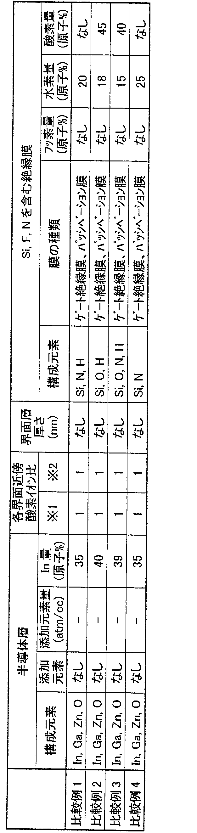

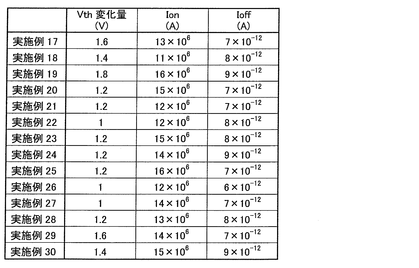

表1~6を参照することにより、半導体層がInおよびOを含み、ゲート絶縁膜およびパッシベーション膜の少なくとも一方がSi、FおよびNを含むことにより、TFTのVthの変化量が抑制されることがわかった。
以上のように本発明の実施の形態および実施例について説明を行なったが、上述の各実施の形態および実施例の構成を適宜組み合わせることも当初から予定している。
今回開示された実施の形態および実施例はすべての点で例示であって、制限的なものではないと考えられるべきである。本発明の範囲は上記した説明ではなくて請求の範囲によって示され、請求の範囲と均等の意味、および範囲内でのすべての変更が含まれることが意図される。
本発明は、絶縁膜およびその製造方法に適用される。また、本発明は、半導体素子に適用される。
1 基板、2,3 シリコンナイトライド膜、10 絶縁膜、20 真空容器、22
天板、24 排気口、26 ガス導入部、32 ホルダ、34 ヒータ、36 軸、38 軸受部、42 マスク、44 仕切り板、50 平面導体、52 給電電極、54 終端電極、56 絶縁フランジ、57,58 パッキン、60 シールドボックス、62 高周波電源、64 整合回路、66 出力カバー、68,69 接続導体、100 プラズマ装置、201 基板、202 ゲート電極、203 ゲート絶縁膜、204 半導体層、205 ソース電極、206 ドレイン電極、207 パッシベーション膜、220,240 界面。
天板、24 排気口、26 ガス導入部、32 ホルダ、34 ヒータ、36 軸、38 軸受部、42 マスク、44 仕切り板、50 平面導体、52 給電電極、54 終端電極、56 絶縁フランジ、57,58 パッキン、60 シールドボックス、62 高周波電源、64 整合回路、66 出力カバー、68,69 接続導体、100 プラズマ装置、201 基板、202 ゲート電極、203 ゲート絶縁膜、204 半導体層、205 ソース電極、206 ドレイン電極、207 パッシベーション膜、220,240 界面。
Claims (16)
- シリコン原子、フッ素原子および窒素原子を含む絶縁膜であって、
酸素原子を含む基板上に配置された第1のシリコンナイトライド膜と、
前記第1のシリコンナイトライド膜に接して配置された第2のシリコンナイトライド膜と、を備え、
前記第2のシリコンナイトライド膜に含まれるフッ素量は、前記第1のシリコンナイトライド膜に含まれるフッ素量よりも多い、絶縁膜。 - シリコン原子とフッ素原子とを含む主ガスと、少なくとも窒素ガスからなる副ガスとのガス流量比を基準値以上に設定して酸素原子を含む基板上に第1のシリコンナイトライド膜を堆積する第1の工程と、
前記主ガスと窒素ガスとのガス流量比を前記基準値よりも小さい値に設定して前記第1のシリコンナイトライド膜に接して第2のシリコンナイトライド膜を堆積する第2の工程とを備える絶縁膜の製造方法。 - 前記副ガスは、水素原子を含むガスと酸素原子を含むガスとのいずれかと、窒素ガスとからなる、請求項2に記載の絶縁膜の製造方法。
- 前記副ガスは、水素原子を含むガスと、窒素ガスとからなる、請求項2に記載の絶縁膜の製造方法。
- 前記基板の表面は、金属によって覆われており、
前記副ガスは、窒素ガスのみからなる、請求項2に記載の絶縁膜の製造方法。 - シリコン原子、フッ素原子および窒素原子を含む絶縁膜と、
インジウム原子および酸素原子を含む酸化物半導体層と、を有する半導体素子。 - 記酸化物半導体層と前記絶縁膜とが接している、請求項6に記載の半導体素子。
- 前記絶縁膜は、ゲート絶縁膜およびパッシベーション膜の少なくとも一方である、請求項6または7に記載の半導体素子。
- 前記絶縁膜における前記フッ素原子の含有量が0原子%より大きく、30原子%以下である、請求項6から8のいずれかに記載の半導体素子。
- 前記絶縁膜は水素原子をさらに含み、前記絶縁膜における水素原子の含有量が0原子%より大きく7原子%以下である、請求項6から9のいずれかに記載の半導体素子。
- 前記絶縁膜は酸素原子をさらに含み、前記絶縁膜における酸素原子の含有量が0原子%より大きく25原子%未満である、請求項6から10のいずれかに記載の半導体素子。
- 前記絶縁膜はゲート絶縁膜であり、前記ゲート絶縁膜と前記半導体層とが接する界面近傍の前記半導体層における酸素量Aと、前記界面近傍以外の前記半導体層における酸素量Bとの比A/Bが0.78よりも大きく、かつ1未満である、請求項6から11のいずれかに記載の半導体素子。
- 前記比A/Bが0.8以上0.98以下である、請求項12に記載の半導体素子。
- 前記絶縁膜はパッシベーション膜であり、前記パッシベーション膜と前記半導体層とが接する界面近傍の前記半導体層における酸素量Cと、前記界面近傍以外の前記半導体層における酸素量Dとの比C/Dが1.05以上1.3以下である、請求項6から13のいずれかに記載の半導体素子。
- 前記半導体層は窒素、アルミニウム、シリコン、チタン、バナジウム、クロム、ジルコニウム、ニオブ、モリブデン、ハフニウム、タンタル、タングステン、スズ、およびビスマスからなる群より選択される1種以上の添加元素をさらに含む、請求項6から14のいずれかに記載の半導体素子。
- 前記半導体素子が薄膜トランジスタであることを特徴とする、請求項6から15のいずれかに記載の半導体素子。
Priority Applications (3)
| Application Number | Priority Date | Filing Date | Title |
|---|---|---|---|
| KR1020187029711A KR20180115808A (ko) | 2011-10-07 | 2012-10-04 | 절연막 및 그 제조 방법 |
| KR1020137035127A KR20140071971A (ko) | 2011-10-07 | 2012-10-04 | 절연막 및 그 제조 방법 |
| CN201280049140.7A CN103875077B (zh) | 2011-10-07 | 2012-10-04 | 绝缘膜及其制造方法 |
Applications Claiming Priority (4)
| Application Number | Priority Date | Filing Date | Title |
|---|---|---|---|
| JP2011-222996 | 2011-10-07 | ||
| JP2011222996A JP5984354B2 (ja) | 2011-10-07 | 2011-10-07 | 半導体素子 |
| JP2012-009098 | 2012-01-19 | ||
| JP2012009098A JP6046351B2 (ja) | 2012-01-19 | 2012-01-19 | 絶縁膜およびその製造方法 |
Publications (1)
| Publication Number | Publication Date |
|---|---|
| WO2013051644A1 true WO2013051644A1 (ja) | 2013-04-11 |
Family
ID=48043797
Family Applications (1)
| Application Number | Title | Priority Date | Filing Date |
|---|---|---|---|
| PCT/JP2012/075774 Ceased WO2013051644A1 (ja) | 2011-10-07 | 2012-10-04 | 絶縁膜およびその製造方法 |
Country Status (4)
| Country | Link |
|---|---|
| KR (2) | KR20140071971A (ja) |
| CN (1) | CN103875077B (ja) |
| TW (1) | TWI541900B (ja) |
| WO (1) | WO2013051644A1 (ja) |
Cited By (3)
| Publication number | Priority date | Publication date | Assignee | Title |
|---|---|---|---|---|
| CN103794652A (zh) * | 2014-02-25 | 2014-05-14 | 华南理工大学 | 金属氧化物半导体薄膜晶体管及其制备方法 |
| JP2015176885A (ja) * | 2014-03-13 | 2015-10-05 | 東京エレクトロン株式会社 | 半導体デバイス、その製造方法、及びその製造装置 |
| WO2022130912A1 (ja) * | 2020-12-18 | 2022-06-23 | 日新電機株式会社 | 薄膜トランジスタの製造方法 |
Families Citing this family (1)
| Publication number | Priority date | Publication date | Assignee | Title |
|---|---|---|---|---|
| JP5790893B1 (ja) * | 2015-02-13 | 2015-10-07 | 日新電機株式会社 | 膜形成方法および薄膜トランジスタの作製方法 |
Citations (4)
| Publication number | Priority date | Publication date | Assignee | Title |
|---|---|---|---|---|
| JP2006165529A (ja) * | 2004-11-10 | 2006-06-22 | Canon Inc | 非晶質酸化物、及び電界効果型トランジスタ |
| JP2009170896A (ja) * | 2007-12-18 | 2009-07-30 | Semiconductor Energy Lab Co Ltd | 半導体装置、および半導体装置の作製方法 |
| JP2010056539A (ja) * | 2008-07-31 | 2010-03-11 | Semiconductor Energy Lab Co Ltd | 半導体装置及びその作製方法 |
| JP2011135055A (ja) * | 2009-11-24 | 2011-07-07 | Semiconductor Energy Lab Co Ltd | 不揮発性メモリ |
Family Cites Families (3)
| Publication number | Priority date | Publication date | Assignee | Title |
|---|---|---|---|---|
| AU2005302962B2 (en) * | 2004-11-10 | 2009-05-07 | Canon Kabushiki Kaisha | Amorphous oxide and field effect transistor |
| US7910929B2 (en) * | 2007-12-18 | 2011-03-22 | Semiconductor Energy Laboratory Co., Ltd. | Semiconductor device |
| JP5679143B2 (ja) * | 2009-12-01 | 2015-03-04 | ソニー株式会社 | 薄膜トランジスタならびに表示装置および電子機器 |
-
2012
- 2012-10-04 KR KR1020137035127A patent/KR20140071971A/ko not_active Ceased
- 2012-10-04 KR KR1020187029711A patent/KR20180115808A/ko not_active Ceased
- 2012-10-04 CN CN201280049140.7A patent/CN103875077B/zh not_active Expired - Fee Related
- 2012-10-04 WO PCT/JP2012/075774 patent/WO2013051644A1/ja not_active Ceased
- 2012-10-05 TW TW101137001A patent/TWI541900B/zh not_active IP Right Cessation
Patent Citations (4)
| Publication number | Priority date | Publication date | Assignee | Title |
|---|---|---|---|---|
| JP2006165529A (ja) * | 2004-11-10 | 2006-06-22 | Canon Inc | 非晶質酸化物、及び電界効果型トランジスタ |
| JP2009170896A (ja) * | 2007-12-18 | 2009-07-30 | Semiconductor Energy Lab Co Ltd | 半導体装置、および半導体装置の作製方法 |
| JP2010056539A (ja) * | 2008-07-31 | 2010-03-11 | Semiconductor Energy Lab Co Ltd | 半導体装置及びその作製方法 |
| JP2011135055A (ja) * | 2009-11-24 | 2011-07-07 | Semiconductor Energy Lab Co Ltd | 不揮発性メモリ |
Cited By (6)
| Publication number | Priority date | Publication date | Assignee | Title |
|---|---|---|---|---|
| CN103794652A (zh) * | 2014-02-25 | 2014-05-14 | 华南理工大学 | 金属氧化物半导体薄膜晶体管及其制备方法 |
| JP2015176885A (ja) * | 2014-03-13 | 2015-10-05 | 東京エレクトロン株式会社 | 半導体デバイス、その製造方法、及びその製造装置 |
| WO2022130912A1 (ja) * | 2020-12-18 | 2022-06-23 | 日新電機株式会社 | 薄膜トランジスタの製造方法 |
| JP2022097012A (ja) * | 2020-12-18 | 2022-06-30 | 日新電機株式会社 | 薄膜トランジスタの製造方法 |
| TWI801019B (zh) * | 2020-12-18 | 2023-05-01 | 日商日新電機股份有限公司 | 薄膜電晶體的製造方法 |
| JP7696076B2 (ja) | 2020-12-18 | 2025-06-20 | 日新電機株式会社 | 薄膜トランジスタの製造方法 |
Also Published As
| Publication number | Publication date |
|---|---|
| TWI541900B (zh) | 2016-07-11 |
| KR20180115808A (ko) | 2018-10-23 |
| CN103875077A (zh) | 2014-06-18 |
| KR20140071971A (ko) | 2014-06-12 |
| TW201324616A (zh) | 2013-06-16 |
| CN103875077B (zh) | 2016-09-28 |
Similar Documents
| Publication | Publication Date | Title |
|---|---|---|
| Oh et al. | Improving the gate stability of ZnO thin-film transistors with aluminum oxide dielectric layers | |
| KR101468591B1 (ko) | 산화물 반도체 및 이를 포함하는 박막 트랜지스터 | |
| TWI438294B (zh) | 藉由利用氮氣之鋅靶材的反應性濺鍍所產生的薄膜半導體材料 | |
| JP5552440B2 (ja) | トランジスタの製造方法 | |
| JP5984354B2 (ja) | 半導体素子 | |
| KR20080076747A (ko) | 산화물 반도체층 형성 방법 및 이를 이용한 반도체 소자제조방법 | |
| KR20070102969A (ko) | 비정질 ZnO계 TFT의 제조방법 | |
| KR20130018300A (ko) | 박막 트랜지스터의 반도체층용 산화물 및 스퍼터링 타깃, 및 박막 트랜지스터 | |
| JP6659255B2 (ja) | 薄膜トランジスタ | |
| JPWO2014168224A1 (ja) | 酸化物半導体ターゲット、酸化物半導体膜及びその製造方法、並びに薄膜トランジスタ | |
| WO2020257314A1 (en) | Method of forming inductively coupled high density plasma films for thin film transistor structures | |
| CN103875077B (zh) | 绝缘膜及其制造方法 | |
| CN115735269A (zh) | 薄膜晶体管 | |
| TWI779254B (zh) | 薄膜電晶體的製造方法 | |
| Sung et al. | Vacuum-free solution-based metallization (VSM) of a-IGZO using trimethylaluminium solution | |
| JP7711340B1 (ja) | 酸化物半導体膜並びにその製造方法、トランジスタ、半導体デバイス、電子回路、電気機器、電子機器、車両、及び動力機関 | |
| JPWO2014136916A1 (ja) | 酸窒化物半導体薄膜 | |
| CN103545377B (zh) | 一种氧化物薄膜晶体管及其制造方法 | |
| CN106796888A (zh) | 半导体器件及其制造方法 | |
| JP2016225505A (ja) | 薄膜トランジスタおよびその製造方法ならびにスパッタリングターゲット | |
| Ochi et al. | Improvement of stress stability in back channel etch-type amorphous In-Ga-Zn-O thin film transistors with post process annealing | |
| WO2016035554A1 (ja) | 薄膜トランジスタの酸化物半導体薄膜、薄膜トランジスタ、およびスパッタリングターゲット | |
| Lee et al. | Characteristics of Ultrathin Indium Oxide Thin‐Film Transistors with Diverse Channel Lengths Fabricated by Atomic Layer Deposition | |
| CN119234318A (zh) | 层叠结构及薄膜晶体管 | |
| WO2016035503A1 (ja) | 薄膜トランジスタ |
Legal Events
| Date | Code | Title | Description |
|---|---|---|---|
| 121 | Ep: the epo has been informed by wipo that ep was designated in this application |
Ref document number: 12838080 Country of ref document: EP Kind code of ref document: A1 |
|
| ENP | Entry into the national phase |
Ref document number: 20137035127 Country of ref document: KR Kind code of ref document: A |
|
| NENP | Non-entry into the national phase |
Ref country code: DE |
|
| 122 | Ep: pct application non-entry in european phase |
Ref document number: 12838080 Country of ref document: EP Kind code of ref document: A1 |