WO2013021467A1 - 変位量モニタ電極の構造 - Google Patents
変位量モニタ電極の構造 Download PDFInfo
- Publication number
- WO2013021467A1 WO2013021467A1 PCT/JP2011/068177 JP2011068177W WO2013021467A1 WO 2013021467 A1 WO2013021467 A1 WO 2013021467A1 JP 2011068177 W JP2011068177 W JP 2011068177W WO 2013021467 A1 WO2013021467 A1 WO 2013021467A1
- Authority
- WO
- WIPO (PCT)
- Prior art keywords
- electrode
- movable electrode
- displacement
- axis direction
- displacement amount
- Prior art date
Links
Images


Classifications
-
- G—PHYSICS
- G01—MEASURING; TESTING
- G01B—MEASURING LENGTH, THICKNESS OR SIMILAR LINEAR DIMENSIONS; MEASURING ANGLES; MEASURING AREAS; MEASURING IRREGULARITIES OF SURFACES OR CONTOURS
- G01B7/00—Measuring arrangements characterised by the use of electric or magnetic techniques
- G01B7/14—Measuring arrangements characterised by the use of electric or magnetic techniques for measuring distance or clearance between spaced objects or spaced apertures
-
- G—PHYSICS
- G01—MEASURING; TESTING
- G01C—MEASURING DISTANCES, LEVELS OR BEARINGS; SURVEYING; NAVIGATION; GYROSCOPIC INSTRUMENTS; PHOTOGRAMMETRY OR VIDEOGRAMMETRY
- G01C19/00—Gyroscopes; Turn-sensitive devices using vibrating masses; Turn-sensitive devices without moving masses; Measuring angular rate using gyroscopic effects
- G01C19/56—Turn-sensitive devices using vibrating masses, e.g. vibratory angular rate sensors based on Coriolis forces
- G01C19/5719—Turn-sensitive devices using vibrating masses, e.g. vibratory angular rate sensors based on Coriolis forces using planar vibrating masses driven in a translation vibration along an axis
- G01C19/5733—Structural details or topology
-
- B—PERFORMING OPERATIONS; TRANSPORTING
- B81—MICROSTRUCTURAL TECHNOLOGY
- B81B—MICROSTRUCTURAL DEVICES OR SYSTEMS, e.g. MICROMECHANICAL DEVICES
- B81B3/00—Devices comprising flexible or deformable elements, e.g. comprising elastic tongues or membranes
- B81B3/0064—Constitution or structural means for improving or controlling the physical properties of a device
- B81B3/0086—Electrical characteristics, e.g. reducing driving voltage, improving resistance to peak voltage
-
- B—PERFORMING OPERATIONS; TRANSPORTING
- B81—MICROSTRUCTURAL TECHNOLOGY
- B81B—MICROSTRUCTURAL DEVICES OR SYSTEMS, e.g. MICROMECHANICAL DEVICES
- B81B2201/00—Specific applications of microelectromechanical systems
- B81B2201/03—Microengines and actuators
- B81B2201/033—Comb drives
Definitions
- the present invention has been made in view of the above points, and even when the relative relationship between the fixed electrode and the movable electrode changes, the amount of displacement that can maintain the amplitude of the detection mass at a constant target amplitude.
- An object is to provide a structure of a monitor electrode.
- the electrode finger 42 of the fixed electrode 32 and the electrode finger 52 of the movable electrode 34 that are adjacent to each other in the Y-axis direction overlap each other in the thickness direction, that is, in the Z-axis direction (that is, the thickness of the electrode finger 42 and the electrode finger 52
- the height (Tm) of the portion facing the side wall of the electrode finger 42 in the Z-axis direction may be different from the thickness of the electrode finger 42 in the Z-axis direction or the thickness of the electrode finger 52 in the Z-axis direction. It may be a thing.
- the electrode fingers 42 that contribute to the reduction of the facing area between the fixed electrode 32 and the movable electrode 34 are the long electrode finger 42-1 and the T-shaped electrode finger 42-3. Projections 46 and 48.
- the area where the fixed electrode 32 and the movable electrode 34 face each other with a gap length d0 is reduced proportionally according to the displacement of the movable electrode 34, and the decreasing slope of the area is the fourth and fourth described above. It becomes larger than the decreasing slope in the process of 5. For this reason, in the sixth process, the capacitance change ⁇ C between the fixed electrode 32 and the movable electrode 34 decreases with a larger slope than the slopes in the fourth and fifth processes. .
- the fixed electrode 32 separated from the movable electrode 34 by the gap length d0 in the Y-axis direction.
- the electrode fingers 42 contributing to the increase in the facing area between the fixed electrode 32 and the movable electrode 34 are the long electrode finger 42-1 and the short electrode finger 42-2.
- the area where the fixed electrode 32 and the movable electrode 34 face each other with a gap length d0 increases in proportion to the displacement of the movable electrode 34.
- the capacitance change amount ⁇ C between the fixed electrode 32 and the movable electrode 34 increases with the same slope as that in the sixth process.
- the fixed electrode 32 separated from the movable electrode 34 by the gap length d0 in the Y-axis direction.
- the long electrode finger 42-1 is the only electrode finger 42 that contributes to an increase in the facing area between the fixed electrode 32 and the movable electrode 34.
- the area where the fixed electrode 32 and the movable electrode 34 face each other with a gap length d0 is proportionally increased according to the displacement of the movable electrode 34, and the increasing slope of the area is the seventh step. It becomes smaller than the increasing slope at. For this reason, in the above-described eighth process, the amount of change in capacitance ⁇ C between the fixed electrode 32 and the movable electrode 34 increases with a smaller gradient than the gradient in the seventh process.
- the displacement amount monitor electrode 10 has a structure in which the change sensitivity of the capacitance change amount ⁇ C described above is greater than that before reaching the target displacement amount A0 after the drive displacement of the movable electrode 34 has reached the target displacement amount A0. And the drive displacement of the movable electrode 34 is larger after reaching the target displacement amount -A0 than before reaching the target displacement amount -A0.
- the fixed electrode 32 and the movable electrode 34 (in particular, the fixed electrode 32) have a change sensitivity of the total area of the surfaces where the electrode fingers 42 and 52 face each other with the gap length d0, and the drive displacement of the movable electrode 34 is small.
- the change sensitivity of the capacitance change amount ⁇ C is higher than that when the movable electrode 34 is positioned between the target displacement amounts ⁇ A0 and A0.
- the fixed displacement of the movable electrode 34 with respect to the drive displacement amount x is changed by the change in the gap between the fixed electrode 32 and the movable electrode 34 and the facing area.
- the capacitance change ⁇ C between the fixed electrode 32 and the movable electrode 34 which occurs when the slope of the capacitance change ⁇ C between the electrode 32 and the movable electrode 34 fluctuates, reaches the target capacitance change C0. Variation of the driving displacement amount x of the movable electrode 34 is reduced.
- the gap between the tip of the electrode finger 42 and the base 50 of the fixed electrode 32 and the movable electrode 34 and the gap between the base 40 and the tip of the electrode finger 52 are reduced. It is not necessary, and it is possible to provide a margin for these gaps.
- the separating portions 86 and 96 are arranged at a predetermined distance from the short electrode fingers 84 and 94 in the X-axis direction.
- a predetermined gap length is formed in the X-axis direction between the separating portions 86 and 96 and the short electrode fingers 84 and 94.
- the separation portions 86 and 96 and the short electrode fingers 84 and 94 constitute an electrode finger having a notch in which a hole having a predetermined gap length is opened.
- the electrode finger 52 of the movable electrode 34 and the long electrode fingers 82 and 92 of the fixed electrode 32 adjacent to each other in the Y-axis direction the electrode finger 52 and the fixed electrode 32 of the movable electrode 34 that can be adjacent to each other in the Y-axis direction.
- a predetermined gap length in the Y-axis direction is formed between the short electrode fingers 84 and 94 and between the electrode finger 52 of the movable electrode 34 and the separating portions 86 and 96 of the fixed electrode 32 adjacent to each other in the Y-axis direction. d0 is formed.
- the electrode fingers 80 and 90 of the fixed electrode 32 and the electrode fingers 52 of the movable electrode 34 adjacent to each other in the Y-axis direction overlap with each other in the thickness direction, that is, the Z-axis direction (that is, the side walls of the electrode fingers 80 and 90).
- the height (Tm) of the portion where the electrode finger 52 and the side wall of the electrode finger 52 face each other in the Z-axis direction may be different from the thickness of the electrode fingers 80 and 90 in the Z-axis direction or the thickness of the electrode finger 52 in the Z-axis direction. It may be the same as both thicknesses.
- the structure of the modified example of the displacement monitor electrode 10 also has a drive displacement amount x in the X-axis direction of the movable electrode 34 when the drive displacement amount x of the movable electrode 34 is between the target displacement amounts -A0 and A0.
- the change sensitivity of the capacitance change amount ⁇ C between the fixed electrode 32 and the movable electrode 34 is relatively small while the drive displacement amount x of the movable electrode 34 satisfies x ⁇ A0 or x> A0, The change sensitivity is relatively large.
- the change sensitivity of the capacitance change amount ⁇ C described above becomes larger after the driving displacement of the movable electrode 34 reaches the target displacement amounts A0, ⁇ A0 than before reaching the target displacement amounts A0, ⁇ A0. It has characteristics. Specifically, in the fixed electrode 32 and the movable electrode 34, the change sensitivity of the total area of the surfaces where the electrode fingers 80, 90 and the electrode finger 52 face each other with the gap length d0 is the target displacement amount. After reaching A0, -A0, the fixed electrode 32 is formed to be larger than before reaching the target displacements A0, -A0. In other words, the fixed electrode 32 includes the electrode fingers 80, 90 and the electrode fingers 52.
- the number of opposing portions with the gap length d0 is formed so as to increase after the driving displacement of the movable electrode 34 reaches the target displacement amounts A0, -A0 as compared to before reaching the target displacement amounts A0, -A0. Yes. Therefore, also in the structure of this modification, the same effect as the structure of the first embodiment described above can be obtained.
- the gap lengths in which the electrode fingers 80 and 90 of the fixed electrode 32 and the electrode fingers 52 of the movable electrode 34 face each other in the Y-axis direction can be equally spaced at all parts.
- the configuration can be made compact, and the area occupied by the displacement monitor electrode 10 on the semiconductor substrate 14 can be prevented from increasing.
- FIG. 10 shows a top view of the displacement monitor electrode 100 according to the second embodiment of the present invention.
- the same components as those shown in FIG. 2 are designated by the same reference numerals, and the description thereof is omitted or simplified.
- FIG. 11 shows the figure showing the operation
- the displacement amount monitor electrode 100 of this embodiment includes a fixed electrode 32 and a movable electrode 34.
- the fixed electrode 32 is formed in a comb-teeth shape and has electrode fingers 102 extending from the base 40 in the X-axis direction parallel to the semiconductor substrate 14.
- a plurality of electrode fingers 102 are provided in parallel with each other with respect to one base 40 and arranged at equal intervals in the Y-axis direction.
- Each electrode finger 102 has the same shape.
- Each electrode finger 102 is formed in a square cross section, and is configured such that the cross-sectional area changes from the connecting portion with the base 40 to the tip.
- each electrode finger 102 has a width in the Y-axis direction of a portion in the vicinity of the connection portion with the base 40 and in the vicinity of the tip in the Y-axis direction, which is larger than the width in the Y-axis direction of the intermediate portion.
- the cross-sectional area of the portion in the vicinity of the connecting portion and the vicinity of the tip is configured to be larger than the cross-sectional area of the intermediate portion.
- a portion in the vicinity of the connection portion with the base 40 having a relatively large cross-sectional area is referred to as the root portion 102-1 and a portion in the vicinity of the tip having a relatively large cross-sectional area is referred to as the tip portion 102-2.
- the intermediate portion having a relatively small cross-sectional area is referred to as an intermediate portion 102-3.
- the fixed electrode 32 and the movable electrode 34 are arranged so that the base portions 40 and 50 face each other in the X-axis direction, and the electrode finger 102 and the electrode finger 52 face each other in the Y-axis direction.
- each electrode finger 52 of the movable electrode 34 is disposed so as to enter the center position of two electrode fingers 102 adjacent to each other in the Y-axis direction of the fixed electrode 32.
- the electrode finger 52 of the movable electrode 34 and the electrode finger 102 of the fixed electrode 32 that are adjacent to each other in the Y-axis direction are formed so that different gap lengths dm are formed in the Y-axis direction depending on the part.
- the gap length between the finger 52 and the root portion 102-1 and the gap length between the electrode finger 52 and the tip portion 102-2 are relatively small and the gap length between the electrode finger 52 and the intermediate portion 102-3. Is configured to be relatively large.
- Each electrode finger 52 of the movable electrode 34 is the vibration center of the structures 16 and 18 (that is, the displacement center of the movable electrode 34) and the tip of the electrode finger 52 of the intermediate portion 102-3 of the electrode finger 102 of the fixed electrode 32 in the X-axis direction. It is configured to be located in the middle in the X-axis direction. Further, the length of the intermediate portion 102-3 in the X-axis direction, that is, the distance between the root portion 102-1 and the tip portion 102-2 in the X-axis direction is the target amplitude of the structures 16 and 18 (that is, its target). The target displacement amount from the vibration center at the tip of the movable electrode 34 corresponding to the amplitude) is set to be equal to or slightly smaller than the value twice A0.
- the electrode finger 102 of the fixed electrode 32 and the electrode finger 52 of the movable electrode 34 that are adjacent to each other in the Y-axis direction overlap each other in the thickness direction, that is, in the Z-axis direction (that is, the thickness of the electrode finger 102 and the electrode finger 52
- the height (Tm) of the portion facing the side wall of the electrode finger 102 in the Z-axis direction may be different from the thickness of the electrode finger 102 in the Z-axis direction or the thickness of the electrode finger 52 in the Z-axis direction, and is equal to both thicknesses. It may be a thing.
- the electrode finger 102 that contributes to the increase in the facing area between the fixed electrode 32 and the movable electrode 34 among the fixed electrodes 32 facing the movable electrode 34 is the intermediate portion 102-3.
- the gap length dm between the electrode finger 102 of the fixed electrode 32 and the electrode finger 52 of the movable electrode 34 in the Y-axis direction is a constant value that is relatively large. For this reason, in the first process described above, the capacitance change amount ⁇ C between the fixed electrode 32 and the movable electrode 34 increases with a constant slope.
- the fixed electrode facing the movable electrode 34 is fixed.
- the electrode finger 102 that contributes to an increase in the facing area between the fixed electrode 32 and the movable electrode 34 among the 32 is a root portion 102-1.
- the gap length dm between the electrode finger 102 of the fixed electrode 32 and the electrode finger 52 of the movable electrode 34 in the Y-axis direction is a constant value that is relatively small. For this reason, in the second process, the capacitance change ⁇ C between the fixed electrode 32 and the movable electrode 34 increases with a larger slope than the slope in the first process.
- the electrode finger 102 that contributes to the reduction of the facing area between the fixed electrode 32 and the movable electrode 34 among the fixed electrodes 32 facing the movable electrode 34 becomes the intermediate part 102-3.
- the gap length dm between the electrode finger 102 of the fixed electrode 32 and the electrode finger 52 of the movable electrode 34 in the Y-axis direction is a constant value that is relatively large.
- the capacitance change amount ⁇ C between the fixed electrode 32 and the movable electrode 34 decreases with a smaller inclination than the inclination in the third process. .
- the electrode finger 102 that contributes to the reduction of the facing area between the fixed electrode 32 and the movable electrode 34 among the fixed electrodes 32 to be formed becomes the tip portion 102-2.
- the gap length dm between the electrode finger 102 of the fixed electrode 32 and the electrode finger 52 of the movable electrode 34 in the Y-axis direction is a constant value that is relatively small.
- the capacitance change ⁇ C between the fixed electrode 32 and the movable electrode 34 decreases with a larger slope than the slopes in the fourth and fifth processes. .
- the fixed electrode 32 and the movable electrode 34 among the fixed electrodes 32 facing the movable electrode 34 are a tip portion 102-2.
- the gap length dm between the electrode finger 102 of the fixed electrode 32 and the electrode finger 52 of the movable electrode 34 in the Y-axis direction is a constant value that is relatively small. For this reason, in the seventh process, the capacitance change amount ⁇ C between the fixed electrode 32 and the movable electrode 34 increases with the same slope as that in the sixth process.
- the fixed electrode 32 and the movable electrode 34 among the fixed electrodes 32 facing the movable electrode 34 The electrode finger 102 that contributes to the increase in the facing area becomes the intermediate portion 102-3.
- the gap length dm between the electrode finger 102 of the fixed electrode 32 and the electrode finger 52 of the movable electrode 34 in the Y-axis direction is a constant value that is relatively large. For this reason, in the above-described eighth process, the amount of change in capacitance ⁇ C between the fixed electrode 32 and the movable electrode 34 increases with a smaller gradient than the gradient in the seventh process.
- the structure of the displacement monitor electrode 100 also has a drive displacement amount x in the X-axis direction of the movable electrode 34 when the drive displacement amount x of the movable electrode 34 is between the target displacement amounts -A0 and A0.
- the change sensitivity of the capacitance change amount ⁇ C between the fixed electrode 32 and the movable electrode 34 is relatively small while the drive displacement amount x of the movable electrode 34 satisfies x ⁇ A0 or x> A0, The change sensitivity is relatively large.
- the displacement monitor electrode 100 has a structure in which the change sensitivity of the capacitance change amount ⁇ C described above is greater than that before reaching the target displacement amount A0 after the drive displacement of the movable electrode 34 reaches the target displacement amount A0. And the drive displacement of the movable electrode 34 is larger after reaching the target displacement amount -A0 than before reaching the target displacement amount -A0.
- the fixed electrode 32 and the movable electrode 34 (particularly, the fixed electrode 32) have a gap length dm where the electrode fingers 102 and 52 face each other (particularly, a gap length where the tip of the electrode finger 52 faces the electrode finger 102).
- the change sensitivity of the capacitance change amount ⁇ C is higher than that when the movable electrode 34 is positioned between the target displacement amounts ⁇ A0 and A0. Therefore, also in the structure of the displacement monitor electrode 100 of the present embodiment, the same effect as the structure of the displacement monitor electrode 10 of the first embodiment can be obtained.
- the gap length in which each part of the electrode finger 102 of the fixed electrode 32 and the electrode finger 52 of the movable electrode 34 are adjacent to each other in the Y-axis direction, and the Y-axis direction of the fixed electrode 32 Since the gap lengths adjacent to each other between the electrode fingers 102 adjacent to each other in the Y-axis direction can be equally spaced, the configuration can be simplified and made compact compared to a structure having a non-uniform gap length. be able to.
- the gap length dm where the electrode fingers 102 and 52 of the fixed electrode 32 and the movable electrode 34 face each other is set.
- the electrode finger 52 of the movable electrode 34 extends from the connection portion with the base portion 50 to the tip in order to make it smaller than before reaching the target displacement amount A0.
- the electrode fingers 102 of the fixed electrode 32 have the same cross-sectional area and the cross-sectional area that changes from the connection portion with the base 40 to the tip.
- the present invention is not limited to this, and the fixed electrode
- Each of the 32 electrode fingers and the electrode finger of the movable electrode 34 may have a cross-sectional area that varies from the connection portion with the base portion to the tip end.
- the electrode finger 120 of the fixed electrode 32 includes a root portion 120-1 having a relatively large cross-sectional area in the vicinity of the connection portion with the base 40 and a tip portion 120 having a relatively large cross-sectional area in the vicinity of the tip.
- -2 and the intermediate portion 120-3 having a relatively small cross-sectional area
- the electrode finger 122 of the movable electrode 34 has a root portion 122 having a relatively large cross-sectional area in the vicinity of the connection portion with the base 50.
- ⁇ 1 a tip portion 122-2 having a relatively large cross-sectional area in the vicinity of the tip, and an intermediate portion 122-3 having a relatively small cross-sectional area.
- the change sensitivity of the capacitance change amount ⁇ C between the fixed electrode 32 and the movable electrode 34 after the drive displacement of the movable electrode 34 reaches the target displacement amounts A0, ⁇ A0 is movable. Since the drive displacement of the electrode 34 becomes larger than the change sensitivity before reaching the target displacement amounts A0, -A0, the effect can be made more remarkable than that of the second embodiment. .
- the electrode finger 130 of the fixed electrode 32 includes a root portion 130-1 having a relatively large cross-sectional area in the vicinity of the connection portion with the base 40, and a base portion 130-2 having a relatively small cross-sectional area.
- the electrode finger 132 of the movable electrode 34 includes a root portion 132-1 having a relatively large cross-sectional area in the vicinity of the connecting portion with the base 50 and a tip portion 132 having a relatively large cross-sectional area in the vicinity of the tip. -2 and an intermediate portion 132-3 having a relatively small cross-sectional area.
- the change sensitivity of the capacitance change amount ⁇ C between the fixed electrode 32 and the movable electrode 34 after the drive displacement of the movable electrode 34 reaches the target displacement amount A0 is Since the driving displacement becomes larger than the change sensitivity before reaching the target displacement amount A0, the effect can be made more remarkable than that of the second embodiment.
- the electrode finger 140 of the fixed electrode 32 includes a root portion 140-1 having a relatively large cross-sectional area in the vicinity of the connection portion with the base 40, and a base portion 140-2 having a relatively small cross-sectional area.
- the electrode finger 142 of the movable electrode 34 includes a base portion 142-1 having a relatively small cross-sectional area and a tip portion 142-2 having a relatively large cross-sectional area in the vicinity of the connecting portion with the base 50. It is good also as what consists of.
- the change sensitivity of the capacitance change amount ⁇ C between the fixed electrode 32 and the movable electrode 34 after the drive displacement of the movable electrode 34 reaches the target displacement amount A0 is Since the driving displacement becomes larger than the change sensitivity before reaching the target displacement amount A0, the effect can be made more remarkable than that of the second embodiment.
- FIG. 15 shows the structure of the modification shown in FIG. 13
- the gap length for each portion where the electrode finger of the fixed electrode 32 and the electrode finger of the movable electrode 34 face each other in the Y-axis direction, and the electrode fingers adjacent to each other in the Y-axis direction of the fixed electrode 32 The gap lengths for each part are equally spaced (that is, as shown in FIG.
- FIG. 16 shows a top view of a displacement monitor electrode 200 according to the third embodiment of the present invention.
- the same components as those shown in FIG. 2 are designated by the same reference numerals, and the description thereof is omitted or simplified.
- FIG. 17 shows the figure showing the operation
- the displacement monitor electrode 200 of this embodiment includes a fixed electrode 32 and a movable electrode 34.
- the fixed electrode 32 is formed in a comb-like shape, and has electrode fingers 202 extending from the base 40 in the X-axis direction parallel to the semiconductor substrate 14.
- a plurality of electrode fingers 202 are provided in parallel with each other with respect to one base 40 and arranged at equal intervals in the Y-axis direction.
- Each electrode finger 202 has the same shape.
- Each electrode finger 202 is formed to have a square cross-section, and is configured such that the cross-sectional area changes from the connection portion with the base 40 to the tip.
- each electrode finger 202 has a base portion in which the thickness in the Z-axis direction of the portion in the vicinity of the connection portion with the base portion 40 and the vicinity of the tip is larger than the thickness in the Z-axis direction of the intermediate portion. 40 is configured such that the cross-sectional area of the portion in the vicinity of the connecting portion and the vicinity of the tip is larger than the cross-sectional area of the intermediate portion.
- a portion in the vicinity of the connection portion with the base 40 having a relatively large cross-sectional area is referred to as the root portion 202-1 and a portion in the vicinity of the tip having a relatively large cross-sectional area is referred to as the tip portion 202-2.
- the intermediate portion having a relatively small cross-sectional area is referred to as an intermediate portion 202-3.
- the fixed electrode 32 and the movable electrode 34 are arranged such that the base portions 40 and 50 face each other in the X-axis direction, and the electrode finger 202 and the electrode finger 52 face each other in the Y-axis direction.
- each electrode finger 52 of the movable electrode 34 is arranged so as to enter the center position of two electrode fingers 202 adjacent to each other in the Y-axis direction of the fixed electrode 32.
- a predetermined gap length d0 is formed in the Y-axis direction between the electrode finger 52 of the movable electrode 34 and the electrode finger 202 of the fixed electrode 32 that are adjacent to each other in the Y-axis direction.
- Each electrode finger 52 of the movable electrode 34 is a vibration center of the structures 16 and 18 (that is, a displacement center of the movable electrode 34) and a tip of the electrode finger 52 of the electrode finger 202 of the fixed electrode 32 in the X-axis direction. It is configured to be located in the middle in the X-axis direction.
- the length of the intermediate portion 202-3 in the X-axis direction that is, the distance between the root portion 202-1 and the tip portion 202-2 in the X-axis direction is the target amplitude of the structures 16 and 18 (that is, the target portion).
- the target displacement amount from the vibration center at the tip of the movable electrode 34 corresponding to the amplitude) is set to be equal to or slightly smaller than the value twice A0.
- the electrode finger 202 of the fixed electrode 32 and the electrode finger 52 of the movable electrode 34 adjacent to each other in the Y-axis direction have a thickness (that is, the side wall of the electrode finger 202 and the electrode finger at a portion overlapping in the Z-axis direction).
- the thickness between the electrode finger 52 and the root portion 202-1 and the electrode finger 52 are set so that the height (Tm) of the portion facing the side wall 52 in the Z-axis direction differs depending on the portion.
- the tip portion 202-2 are relatively large, and the thickness between the electrode finger 52 and the intermediate portion 202-3 is relatively small.
- the electrode finger 202 that contributes to an increase in the facing area between the fixed electrode 32 and the movable electrode 34 among the fixed electrodes 32 facing the movable electrode 34 is the intermediate portion 202-3.
- the height Tm in the Z-axis direction in which the electrode finger 202 of the fixed electrode 32 and the electrode finger 52 of the movable electrode 34 face each other in the Y-axis direction is a relatively small constant value, and the fixed electrode 32 and the movable electrode The area facing 34 with a gap length d0 is proportionally increased according to the displacement of the movable electrode 34. For this reason, in the first process described above, the capacitance change amount ⁇ C between the fixed electrode 32 and the movable electrode 34 increases with a constant slope.
- the fixed electrode facing the movable electrode 34 is fixed.
- An electrode finger 202 that contributes to an increase in the opposing area of the fixed electrode 32 and the movable electrode 34 among the 32 is a root portion 202-1.
- the height Tm in the Z-axis direction in which the electrode finger 202 of the fixed electrode 32 and the electrode finger 52 of the movable electrode 34 face each other in the Y-axis direction becomes a relatively large constant value
- the fixed electrode 32 and the movable electrode 34 Are proportionally increased in accordance with the displacement of the movable electrode 34, and the increasing slope of the area becomes larger than the increasing slope in the first process described above.
- the capacitance change ⁇ C between the fixed electrode 32 and the movable electrode 34 increases with a larger slope than the slope in the first process.
- the fixed electrode 32 and the movable electrode 34 out of the fixed electrodes 32 opposed to the movable electrode 34.
- the electrode finger 202 that contributes to the reduction of the facing area is the root portion 202-1.
- the height Tm in the Z-axis direction in which the electrode finger 202 of the fixed electrode 32 and the electrode finger 52 of the movable electrode 34 face each other in the Y-axis direction is a constant value that is relatively large.
- the area facing 34 with a gap length d0 is proportionally decreased according to the displacement of the movable electrode 34. For this reason, in the third process, the amount of change in capacitance ⁇ C between the fixed electrode 32 and the movable electrode 34 decreases with the same inclination as that in the second process.
- the electrode finger 202 that contributes to the reduction in the facing area between the fixed electrode 32 and the movable electrode 34 among the fixed electrodes 32 facing the movable electrode 34 becomes the intermediate part 202-3.
- the height Tm in the Z-axis direction in which the electrode finger 202 of the fixed electrode 32 and the electrode finger 52 of the movable electrode 34 face each other in the Y-axis direction becomes a relatively small constant value
- the fixed electrode 32 and the movable electrode 34 Are proportionally decreased according to the displacement of the movable electrode 34, and the decreasing slope of the area becomes smaller than the decreasing slope in the third process.
- the capacitance change amount ⁇ C between the fixed electrode 32 and the movable electrode 34 decreases with a smaller inclination than the inclination in the third process. .
- the height Tm in the Z-axis direction in which the electrode finger 202 of the fixed electrode 32 and the electrode finger 52 of the movable electrode 34 face each other in the Y-axis direction becomes a relatively large constant value
- the fixed electrode 32 and the movable electrode 34 Are proportionally decreased according to the displacement of the movable electrode 34, and the decreasing slope of the area is larger than the decreasing slopes in the fourth and fifth processes described above.
- the capacitance change ⁇ C between the fixed electrode 32 and the movable electrode 34 decreases with a larger slope than the slopes in the fourth and fifth processes. .
- the fixed electrode 32 and the movable electrode 34 among the fixed electrodes 32 facing the movable electrode 34 are the fixed electrode 32 and the movable electrode 34 among the fixed electrodes 32 facing the movable electrode 34.
- the electrode finger 202 that contributes to an increase in the facing area is the tip portion 202-2.
- the height Tm in the Z-axis direction in which the electrode finger 202 of the fixed electrode 32 and the electrode finger 52 of the movable electrode 34 face each other in the Y-axis direction is a constant value that is relatively large.
- the area facing 34 with a gap length d0 is proportionally increased according to the displacement of the movable electrode 34. For this reason, in the seventh process, the capacitance change amount ⁇ C between the fixed electrode 32 and the movable electrode 34 increases with the same slope as that in the sixth process.
- the fixed electrode 32 and the movable electrode 34 among the fixed electrodes 32 facing the movable electrode 34 The electrode finger 202 that contributes to the increase in the facing area becomes the intermediate portion 202-3.
- the height Tm in the Z-axis direction in which the electrode finger 202 of the fixed electrode 32 and the electrode finger 52 of the movable electrode 34 face each other in the Y-axis direction becomes a relatively small constant value, and the fixed electrode 32 and the movable electrode 34 Are proportionally increased according to the displacement of the movable electrode 34, and the increasing slope of the area becomes smaller than the increasing slope in the seventh process.
- the amount of change in capacitance ⁇ C between the fixed electrode 32 and the movable electrode 34 increases with a smaller gradient than the gradient in the seventh process.
- the structure of the displacement monitor electrode 200 is different from the structures of the displacement monitor electrodes 10 and 100 of the first and second embodiments described above, and the electrode finger 202 of the fixed electrode 32 and the electrode finger of the movable electrode 34. 52 have a configuration in which the width in the Y-axis direction does not change from the distal end to the connecting portion between the base portions 40 and 50. Therefore, the electrode finger 202 of the fixed electrode 32 and the electrode finger 52 of the movable electrode 34 are opposed to each other in the Y axis direction, and the electrode fingers 202 adjacent to each other in the Y axis direction of the fixed electrode 32 are adjacent in the Y axis direction.
- the gap lengths of the electrode fingers 52 adjacent to each other in the Y-axis direction of the movable electrode 34 can be made the shortest and equally spaced, so that the gap length is not uniform.
- the configuration can be simplified and made compact, and the area occupied by the displacement monitor electrode 200 on the semiconductor substrate 14 can be prevented from increasing.
- the electrode finger 230 of the fixed electrode 32 has a relatively large cross-sectional area in the vicinity of the base portion 230-1 in the vicinity of the connection portion with the base 40, and a relatively large cross-sectional area.
- the electrode finger 232 of the movable electrode 34 has a root portion 232-1 having a relatively large cross-sectional area in the vicinity of the connecting portion with the base 50, and a cross-sectional area in the vicinity of the tip.
- the tip portion 232-2 having a relatively large cross section and the intermediate portion 232-3 having a relatively small cross-sectional area may be included.
- the change sensitivity of the capacitance change amount ⁇ C between the fixed electrode 32 and the movable electrode 34 after the drive displacement of the movable electrode 34 reaches the target displacement amount A0 is Since the drive displacement becomes larger than the change sensitivity before reaching the target displacement amount A0, the effect can be made more remarkable than that of the third embodiment.
- the displacement amount monitor electrode 200 as a whole has a gap in which the electrode finger of the fixed electrode 32 and the electrode finger of the movable electrode 34 face each other in the Y-axis direction.
- the configuration can be simplified and made compact, and the area occupied by the displacement monitor electrode 200 on the semiconductor substrate 14 can be prevented from increasing.
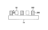
- dielectric materials 304 and 306 are disposed on the surface of the portion in the vicinity of the connection portion with the base portion 40 and the vicinity of the tip.
- the dielectric materials 304 and 306 are provided on both sides of the side surface where the electrode finger 302 faces the electrode finger 52 of the movable electrode 34 in the Y-axis direction.
- the dielectric materials 304 and 306 are made of a highly insulating material or a material having a low Young's modulus or viscosity, which is different from the material of the electrode finger 302 main body.
- the dielectric materials 304 and 306 have a relative dielectric constant larger than the relative dielectric constant “1” of air, and have a predetermined thickness d1 in the Y-axis direction on the surface of the electrode finger 302.
- the dielectric materials 304 and 306 may be manufactured using, for example, an organic material such as a SiO 2 film (oxide insulating film) or a resist material that can be easily deposited by thermally oxidizing silicon.
- an organic material such as a SiO 2 film (oxide insulating film) or a resist material that can be easily deposited by thermally oxidizing silicon.
- a portion near the connection portion with the base 40 provided with the dielectric material 304 is a root portion 302-1 and a portion near the tip provided with the dielectric material 306 is a tip portion 302-. 2 and an intermediate portion between the root portion 302-1 and the tip portion 302-2 is referred to as an intermediate portion 302-3, respectively.
- the fixed electrode 32 and the movable electrode 34 are arranged such that the base portions 40 and 50 face each other in the X-axis direction, and the electrode finger 302 and the electrode finger 52 face each other in the Y-axis direction.
- each electrode finger 52 of the movable electrode 34 is disposed so as to enter the center position of two electrode fingers 302 adjacent to each other in the Y-axis direction of the fixed electrode 32.
- a predetermined gap length d0 in the Y-axis direction at the intermediate portion 302-3 of the electrode finger 302 is formed in the Y-axis direction at the root portion 302-1 and the tip portion 302-2.
- Each electrode finger 52 of the movable electrode 34 is the vibration center of the structures 16 and 18 (that is, the displacement center of the movable electrode 34), and the tip of the electrode finger 52 is the middle portion 302-3 of the electrode finger 302 of the fixed electrode 32 in the X axis direction. It is configured to be located in the middle in the X-axis direction.
- the length of the intermediate portion 302-3 in the X-axis direction is equal to the target amplitude of the structures 16 and 18 (that is, the target displacement amount from the vibration center at the tip of the movable electrode 34 corresponding to the target amplitude) A0. Or slightly smaller than that value.
- the thickness of the electrode finger 302 of the fixed electrode 32 and the electrode finger 52 of the movable electrode 34 adjacent to each other in the Y-axis direction overlap each other in the thickness direction, that is, the Z-axis direction (that is, the side wall of the electrode finger 302 and the electrode finger 52).
- the height (Tm) of the portion facing the side wall of the electrode finger 102 in the Z-axis direction may be different from the thickness of the electrode finger 102 in the Z-axis direction or the thickness of the electrode finger 52 in the Z-axis direction, and is equal to both thicknesses. It may be a thing.
- the electrode finger 302 that contributes to the increase in the facing area between the fixed electrode 32 and the movable electrode 34 among the fixed electrodes 32 facing the movable electrode 34 is the intermediate portion 302-3.
- the capacitance change amount ⁇ C1 between the fixed electrode 32 and the movable electrode 34 increases with a constant slope according to the drive displacement amount x as shown in the following equation (2). Note that the amount of change in the facing area where the fixed electrode 32 and the movable electrode 34 face each other is ⁇ S.
- the amount of change in capacitance ⁇ C2 between the fixed electrode 32 and the movable electrode 34 is, as shown in the following equation (3), the amount of change in capacitance of the dielectric material 304: This is based on the change in capacitance of the space between the dielectric material 304 and the electrode finger 52 of the movable electrode 34 in the Y-axis direction, and the inclination in the first process according to the drive displacement amount x. It increases with a large slope compared to.
- the dielectric constant of the space between the electrode finger 302 of the fixed electrode 32 and the electrode finger 52 of the movable electrode 34 is ⁇ 1
- the dielectric constant of the dielectric material 304 is ⁇ 2 (> ⁇ 1)
- the fixed electrode 32 and the movable electrode 34 are The amount of change in the facing area.
- ⁇ C2 ⁇ 1 ⁇ ⁇ 2 ⁇ ⁇ S / ( ⁇ 2 ⁇ (d0 ⁇ d1) + ⁇ 1 ⁇ d1) (3)
- the fixed electrode 32 and the movable electrode 34 out of the fixed electrodes 32 opposed to the movable electrode 34.
- the electrode finger 302 that contributes to the reduction of the facing area is the root portion 302-1. Therefore, in the third process, the capacitance change amount ⁇ C between the fixed electrode 32 and the movable electrode 34 has the same slope as that in the second process according to the drive displacement amount x. Decrease.
- the electrode finger 302 that contributes to the reduction of the facing area between the fixed electrode 32 and the movable electrode 34 becomes the intermediate portion 302-3. Therefore, in the fourth and fifth processes, the capacitance change amount ⁇ C between the fixed electrode 32 and the movable electrode 34 has a slope in the third process according to the drive displacement amount x. Compared to a small slope, it decreases.
- the amount of change in capacitance ⁇ C between the fixed electrode 32 and the movable electrode 34 is the amount of change in the capacitance of the dielectric material 306 and the amount of change in the dielectric material 306 and the movable electrode 34. It is based on the capacitance change amount of the space between the electrode finger 52 and decreases with a large inclination according to the drive displacement amount x as compared with the inclination in the fourth and fifth processes.
- the fixed electrode 32 and the movable electrode 34 among the fixed electrodes 32 facing the movable electrode 34 The electrode finger 302 that contributes to the increase in the facing area becomes the intermediate portion 302-3. Therefore, in the eighth process, the capacitance change amount ⁇ C between the fixed electrode 32 and the movable electrode 34 is smaller than the slope in the seventh process according to the drive displacement amount x. Increase with slope.
- the structure of the displacement monitor electrode 300 also has a drive displacement amount x in the X-axis direction of the movable electrode 34 when the drive displacement amount x of the movable electrode 34 is between the target displacement amounts -A0 and A0.
- the change sensitivity of the capacitance change amount ⁇ C between the fixed electrode 32 and the movable electrode 34 is relatively small while the drive displacement amount x of the movable electrode 34 satisfies x ⁇ A0 or x> A0, The change sensitivity is relatively large.
- the structure of the displacement monitor electrode 300 has a change sensitivity of the capacitance change amount ⁇ C described above after the drive displacement of the movable electrode 34 reaches the target displacement amount A0 compared to before reaching the target displacement amount A0.
- the drive displacement of the movable electrode 34 is larger after reaching the target displacement amount -A0 than before reaching the target displacement amount -A0.
- the fixed electrode 32 and the movable electrode 34 are arranged in the vicinity of the tip and the connection portion with the base so that the change sensitivity of the capacitance change amount ⁇ C has the above-described characteristics.
- electrode fingers having dielectric materials 304 and 306 disposed thereon.
- the displacement amount monitor electrode 300 when the dielectric materials 304 and 306 are each made of a highly insulating material, in the process in which the structures 16 and 18 vibrate in the X-axis direction, manufacturing variations and control variations, Even if the movable electrode 34 collides with the fixed electrode 32 due to application of excessive stress from the outside, it is avoided that both electrodes 32 and 34 are conducted due to the presence of the dielectric materials 304 and 306. It is possible to detect a change in capacitance between the electrode 32 and the movable electrode 34 with high accuracy, and to prevent a malfunction in driving the structures 16 and 18 in the X-axis direction with respect to the semiconductor substrate 14. Can do.
- the dielectric materials 304 and 306 when they are made of a material having a low Young's modulus or viscosity, they can move due to manufacturing variations, control variations, excessive external stress application, and the like. Even if the electrode 34 collides with the fixed electrode 32, the shock applied to both the electrodes 32 and 34 is absorbed by the presence of the dielectric materials 304 and 306, so that the fixed electrode 32 and the movable electrode 34 can be prevented from being damaged.
- the dielectric materials 304 and 306 are disposed only on the electrode fingers 302 of the fixed electrode 32.
- the present invention is not limited to this, and the movable electrode 34 is further limited.
- a dielectric material may be disposed on the electrode fingers.
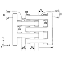
- dielectric materials 324, 326, 328, 330 may be provided in both the fixed electrode 32 and the electrode fingers 320 and 322 of the movable electrode 34.
- the change sensitivity of the capacitance change amount ⁇ C between the fixed electrode 32 and the movable electrode 34 after the drive displacement of the movable electrode 34 reaches the target displacement amounts A0, ⁇ A0 is movable. Since the drive displacement of the electrode 34 becomes larger than the change sensitivity before reaching the target displacement amounts A0, -A0, the effect can be made more remarkable than that of the fourth embodiment. .
- the dielectric material 342 is disposed only in the vicinity of the connection portion with the base 40, and in the electrode finger 344 of the movable electrode 34, the base 50 and Dielectric materials 346 and 348 may be disposed in the vicinity of the connection portion and the vicinity of the tip.
- the change sensitivity of the capacitance change amount ⁇ C between the fixed electrode 32 and the movable electrode 34 after the drive displacement of the movable electrode 34 reaches the target displacement amounts A0, ⁇ A0 is movable. Since the drive displacement of the electrode 34 becomes larger than the change sensitivity before reaching the target displacement amounts A0, -A0, the effect can be made more remarkable than that of the fourth embodiment. .
- the dielectric material 362 is disposed only in the vicinity of the connection portion with the base 40, and the electrode finger 364 of the movable electrode 34 is near the tip.
- the dielectric material 366 may be disposed only at the site.
- both electrodes 32 and 34 are made conductive by the presence of the dielectric material disposed on the fixed electrode 32 and the movable electrode 34. Is avoided, and the impact when the two electrodes 32 and 34 collide is absorbed, so that the same effect as in the fourth embodiment can be obtained.
- the dielectric material 304, 306 having a predetermined thickness d1 is disposed on the surface of the fixed electrode 32, so that the electrode finger 302 of the fixed electrode 32 and the electrode finger 52 of the movable electrode 34 are
- the change sensitivity of the capacitance change amount ⁇ C between the fixed electrode 32 and the movable electrode 34 is changed in accordance with the drive displacement amount of the movable electrode 34. Is not limited to this. That is, the electrode finger 302 of the fixed electrode 32 and the electrode finger 52 of the movable electrode 34 have a configuration in which the width in the Y-axis direction does not change from the tip to the connection portion with the bases 40 and 50.
- the dielectric constant between them is changed, and the above change is made.
- Sensitivity may be realized.
- a dielectric material filled between the surface of the electrode finger 302 of the fixed electrode 32 and the surface of the electrode finger 52 of the movable electrode 34 is applied to the root portion 302-1 and the tip portion 302-2 of the electrode finger 302 of the fixed electrode 32.
- the corresponding part has a relatively high dielectric constant, while the part corresponding to the intermediate portion 302-3 of the electrode finger 302 has a relatively low dielectric constant.
- the dielectric constant between the electrode fingers 302 and 52 facing each other in the Y-axis direction is not reached after the driving displacement of the movable electrode 34 reaches the target displacement amount A0.
- the driving displacement of the movable electrode 34 reaches the target displacement amount -A0, it becomes larger than before the target displacement amount -A0.
- the electrode fingers 302 of the fixed electrode 32 and Each of the electrode fingers 52 of the movable electrode 34 has a configuration in which the width in the Y-axis direction does not change from the tip to the connection portion with the base portions 40 and 50. Therefore, the gap length in which the electrode finger 302 of the fixed electrode 32 and the electrode finger 52 of the movable electrode 34 face each other in the Y-axis direction, and the electrode fingers 302 adjacent to each other in the Y-axis direction of the fixed electrode 32 are adjacent in the Y-axis direction.
- the gap lengths of the electrode fingers 52 adjacent to each other in the Y-axis direction of the movable electrode 34 can be made the shortest and equally spaced, so that the gap length is not uniform.
- the configuration can be simplified and made compact, and the area occupied by the displacement monitor electrode 300 on the semiconductor substrate 14 can be prevented from increasing.
- Displacement monitor electrode 14
- Semiconductor substrate 16 18 Structure
- Fixed electrode 34 Movable electrode 40, 50 Base 42, 52, 80 , 90, 102, 120, 122, 130, 132, 140, 142, 202, 220, 222, 230, 232, 240, 242, 302, 320, 322, 340, 344, 360, 364
Landscapes
- Engineering & Computer Science (AREA)
- Physics & Mathematics (AREA)
- General Physics & Mathematics (AREA)
- Radar, Positioning & Navigation (AREA)
- Remote Sensing (AREA)
- Computer Hardware Design (AREA)
- Microelectronics & Electronic Packaging (AREA)
- Pressure Sensors (AREA)
- Measurement Of Length, Angles, Or The Like Using Electric Or Magnetic Means (AREA)
- Gyroscopes (AREA)
Abstract
本発明の変位量モニタ電極の構造は、固定電極と可動電極との相対的な関係が変化しても、検出マスの振幅を一定の目標振幅に保つうえで、それぞれ基部及び該基部から基板に対して平行な所定軸方向に延びる電極指からなる櫛歯状の、基板に対して固定される固定電極と、所定軸方向に変位し得る可動電極と、が互いの電極指同士が噛み合うように対向配置され、固定電極と可動電極との間の静電容量の変化量に基づいて目標振幅で駆動させるべき検出マスの変位量をモニタする変位量モニタ電極の構造において、可動電極の所定軸方向への変位量に対する静電容量の変化量の変化感度を、該可動電極の該所定軸方向への変位が検出マスの目標振幅に対応する目標変位量に達した後は該目標変位量に達する前に比べて大きくする。
Description
本発明は、変位量モニタ電極の構造に係り、特に、基板に対して固定される固定電極と、基板に対して平行な所定軸方向に変位し得る可動電極と、が互いの電極指同士が噛み合うように対向配置され、固定電極と可動電極との間の静電容量の変化量に基づいて目標振幅で駆動させるべき検出マスの変位量をモニタする変位量モニタ電極の構造に関する。
従来、角速度センサなどを構成し、検出マスを一定の目標振幅で駆動振動させるべくその変位量をモニタする変位量モニタ電極の構造が知られている(例えば、特許文献1参照)。変位量モニタ電極は、櫛歯状の固定電極と櫛歯状の可動電極とを備えている。固定電極は、基部及び該基部から基板に対して平行な所定軸方向に延びる電極指からなり、基板に対して固定されている。また、可動電極は、基部及び該基部から基板に対して平行な所定軸方向に延びる電極指からなり、基板に対して所定軸方向に変位し得る。かかる変位量モニタ電極において、可動電極が基板に対して所定軸方向に変位すると、固定電極と可動電極との間の静電容量が変化する。この際、静電容量の変化量は、可動電極の変位量に応じたものとなる。そして、この静電容量の変化量に基づいて検出マスの変位量(振幅)がモニタされ、その検出マスが目標振幅で駆動するように制御される。
ところで、固定電極と可動電極との間の静電容量の変化量は、一般的に検出マスの振幅に応じて直線的に変化するが、その検出マスの振幅だけでなく、固定電極と可動電極とのギャップや対向面積によっても変化する。具体的には、応力変化や寸法バラツキなどに起因してそのギャップ又は対向面積が変化すると、その変化に応じた分だけ可動電極の変位量に対する静電容量の変化量の感度(傾き)が変化する。この場合において、静電容量の変化量が、検出マスが目標振幅で駆動される過程で常に可動電極の変位量に対して一定の傾きで直線的に変化する領域に設定されている構造では、モニタ電極の組み立て時に加わる応力や温度変化,寸法バラツキなどに起因して固定電極と可動電極とのギャップや対向面積が所望のものに一致していないと、静電容量の変化量が目標容量変化量に達したときに可動電極の変位量が目標変位量に合致しない事態が生じる。具体的には、上記したギャップや対向面積のバラツキによって検出マスの振幅量が目標振幅を基準にして例えば±20%の範囲で変化すると、可動電極の変位量に対する静電容量の変化量の感度も同じ±20%だけ変化することとなる。従って、上記した構造では、検出マスの振幅を一定の目標振幅に保つことが困難となる。
本発明は、上述の点に鑑みてなされたものであり、固定電極と可動電極との相対的な関係が変化しても、検出マスの振幅を一定の目標振幅に保つことが可能な変位量モニタ電極の構造を提供することを目的とする。
上記の目的は、それぞれ基部及び該基部から基板に対して平行な所定軸方向に延びる電極指からなる櫛歯状の、前記基板に対して固定される固定電極と、前記所定軸方向に変位し得る可動電極と、が互いの前記電極指同士が噛み合うように対向配置され、前記固定電極と前記可動電極との間の静電容量の変化量に基づいて目標振幅で駆動させるべき検出マスの変位量をモニタする変位量モニタ電極の構造であって、前記可動電極の前記所定軸方向への変位量に対する前記静電容量の変化量の変化感度は、該可動電極の該所定軸方向への変位が前記目標振幅に対応する目標変位量に達した後は該目標変位量に達する前に比べて大きくなる特性を有する変位量モニタ電極の構造により達成される。
本発明によれば、固定電極と可動電極との相対的な関係が変化しても、検出マスの振幅を一定の目標振幅に保つことができる。
以下、図面を用いて、本発明に係る変位量モニタ電極の構造の具体的な実施形態について説明する。
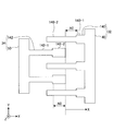
図1は、本発明の第1実施例である変位量モニタ電極10の構造を採用するセンサ12の構成図を示す。本実施例のセンサ12は、例えば車両などに搭載されるX-Y平面に垂直なZ軸回りに生じる角速度を検出するための角速度センサである。センサ12は、シリコンなどの半導体基板14上に形成されており、半導体基板14の表面に微細加工によるエッチングを施すことにより形成される。
センサ12は、互いに等しい質量を有する一対の構造体16,18と、半導体基板14上で構造体16,18をX軸方向に励振駆動するための駆動電極20-1,20-2,22-1,22-2と、半導体基板14上で構造体16,18に生じるY軸方向の振動(振幅)を検出するための検出電極24-1,24-2,26-1,26-2と、半導体基板14上で構造体16,18のX軸方向への駆動変位量をモニタするための変位量モニタ電極28-1,28-2,30-1,30-2と、を有している。構造体16,18は、絶縁層を形成する半導体基板14の表面から所定距離だけ浮いた状態でその半導体基板14上で互いに対称位置に配置されている。以下、変位量モニタ電極28-1,28-2,30-1,30-2を纏める場合は、変位量モニタ電極10とする。
駆動電極20-1,20-2,22-1,22-2及び検出電極24-1,24-2,26-1,26-2はそれぞれ、半導体基板14に対して固定される固定電極と、半導体基板14に対してX軸方向又はY軸方向に可動する可動電極と、からなる。これらの固定電極は、パッドを介して信号処理回路に接続されている。また、これらの可動電極は、構造体16,18の一部を構成している。
駆動電極20-1,20-2,22-1,22-2はそれぞれ、固定電極への駆動電圧の印加によって固定電極と可動電極との間に静電引力を作用させることにより構造体16,18を半導体基板14に対してX軸方向に駆動させるための電極である。また、検出電極部24-1,24-2,26-1,26-2はそれぞれ、構造体16,18のY軸方向の変位に伴う固定電極と可動電極との間の静電容量の変化を検出することにより構造体16,18の半導体基板14に対するY軸方向の振動を検出するための電極である。
具体的には、駆動電極20-1,20-2,22-1,22-2はそれぞれ、信号処理回路からパッドを介して固定電極に構造体16,18の共振周波数にほぼ等しい周波数の駆動電圧が印加されることで固定電極と可動電極との間に静電引力を作用させて、その構造体16,18をその構造体16,18の共振周波数にほぼ等しい周波数でX軸方向に一定振幅で励振駆動する駆動力を発生させる。尚、駆動電極20-1と駆動電極20-2とは互いに同相で駆動力を発生させかつ駆動電極22-1と駆動電極22-2とは互いに同相で駆動力を発生させる一方、駆動電極20-1,20-2と駆動電極22-1,22-2とは互いに逆相で駆動力を発生させる。
また、検出電極24-1,24-2,26-1,26-2ではそれぞれ、構造体16,18に半導体基板14に対してY軸方向に加わる振動変位に応じて、固定電極と可動電極との間で静電容量変化が生じる。尚、検出電極24-1,24-2での静電容量変化と検出電極26-1,26-2での静電容量変化とは、互いに逆相である。検出電極24-1,24-2,26-1,26-2の静電容量変化は、構造体16,18のY軸方向への振動変位量がゼロである場合は略ゼロであって、構造体16,18のY軸方向への振動変位量が大きいほど大きくなる。検出電極24-1,24-2,26-1,26-2の固定電極はそれぞれ、固定電極と可動電極との間の静電容量変化を検出変位信号として信号処理回路へ出力する。この信号処理回路は、各検出電極24-1,24-2,26-1,26-2からの検出変位信号を処理することにより、構造体16,18のY軸方向への振動変位量を検出し、そして、その振動変位量に基づいてZ軸回りに生じる角速度を検出する。
次に、本実施例のセンサ12の動作について説明する。
X軸及びY軸の双方に直交するZ軸回りの角速度の検出が行われる場合、センサ12において、駆動電極20-1,20-2,22-1,22-2が励振駆動される。具体的には、構造体16,18の共振周波数にほぼ等しい周波数を有する駆動電圧が駆動電極20-1,20-2,22-1,22-2の固定電極に印加される。かかる駆動電圧が印加されると、駆動電極20-1,20-2,22-1,22-2それぞれにおいて固定電極と可動電極との間に構造体16,18をX軸方向に励振駆動する駆動力が発生することで、構造体16,18が互いに逆相で共振周波数にほぼ等しい周波数でX軸方向に一定振幅で励振駆動される。
構造体16,18が上記の如くX軸方向に励振駆動されている状態でZ軸回りの角速度が発生していない場合は、構造体16,18にコリオリ力が作用しない。この場合は、検出電極24-1,24-2,26-1,26-2がY軸方向に振動変位せず、検出電極24-1,24-2,26-1,26-2の固定電極と可動電極との間に静電容量変化が生じないので、検出電極24-1,24-2,26-1,26-2から出力される検出変位信号は、構造体16,18のY軸方向の振幅が略ゼロであることを表す信号となる。
一方、構造体16,18が上記の如くX軸方向に励振駆動されている状態でZ軸回りの角速度が発生した場合は、構造体16,18にコリオリ力が作用する。この場合は、かかるコリオリ力の作用により検出電極24-1,24-2,26-1,26-2がY軸方向に振動変位して、検出電極24-1,24-2,26-1,26-2の固定電極と可動電極との間に静電容量変化が生じる。かかる静電容量変化が生じると、検出電極24-1,24-2,26-1,26-2から出力される検出変位信号は、構造体16,18のY軸方向の振幅が発生している角速度の大きさを表す信号となる。構造体16,18は、コリオリ力が作用した際にY軸方向に関し互いに逆相で振動変位する。従って、センサ12によれば、対象にZ軸周りに生じている角速度を検出することができる。
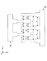
図2は、本実施例の変位量モニタ電極10の上面図を示す。また、図3は、本実施例の変位量モニタ電極10の断面図を示す。
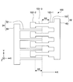
変位量モニタ電極28-1,28-2,30-1,30-2としての変位量モニタ電極10はそれぞれ、半導体基板14に対して固定される固定電極32と、半導体基板14に対してX軸方向に可動する可動電極34と、からなる。固定電極32は、パッドを介して信号処理回路に接続されている。また、可動電極34は、構造体16,18の一部を構成している。変位量モニタ電極10は、構造体16,18のX軸方向の変位に伴う固定電極32と可動電極34との間の静電容量の変化を検出することにより、構造体16,18の半導体基板14に対するX軸方向の駆動変位量(振幅)をモニタするための電極である。
固定電極32は、櫛歯状に形成されており、比較的幅広に延設された基部40、及び、その基部40から半導体基板14に対して平行なX軸方向に棒状に延びる電極指42を有している。基部40は、断面四角状に形成されており、半導体基板14に対して平行なY軸方向に延びている。また、電極指42は、一つの基部40に対して互いに平行にY軸方向に並んで複数本設けられている。電極指42は、X軸方向の長さが比較的長い長尺電極指42-1、X軸方向の長さが比較的短い短尺電極指42-2、及び、X軸方向の長さが比較的長くかつ先端がY軸方向に翼状に広がる形状を有するT型電極指42-3である。
電極指42の長尺電極指42-1及び短尺電極指42-2はそれぞれ、断面四角状に形成されており、基部40との接続部から先端まで同じ断面積(Y軸方向において同じ幅かつZ軸方向において同じ厚さ)を有している。また、T型電極指42-3は、断面四角状に形成されており、基部40との接続部から先端近傍まで同じ断面積(Y軸方向において同じ幅かつZ軸方向において同じ厚さ)を有している。T型電極指42-3は、Y軸方向に延びる先端部44を有している。T型電極指42-3の先端部44のY軸方向両端にはそれぞれ、その先端部44から基部40側へ向けて半導体基板14に対して平行なX軸方向に延びる突部46,48が設けられている。すなわち、先端部44は、上方から見てコノ字状に形成されている。突部46,48は、先端部44との接続部から先端まで同じ断面積(Y軸方向において同じ幅かつZ軸方向において同じ厚さ)を有し、かつ、上記の短尺電極指42-2と同じ断面積を有している。
電極指42は、一つの長尺電極指42-1と二つの短尺電極指42-2と一つのT型電極指42-3とを一セットとしたパターンに形成されている。具体的には、図2に示す如く、Y軸方向において順に長尺電極指42-1、短尺電極指42-2、T型電極指42-3、及び短尺電極指42-2が構成されると共に、その構成がY軸方向において繰り返されるように形成されている。電極指42は、一つのT型電極指42-3を挟んでY軸方向両側に短尺電極指42-2及び長尺電極指42-1が一つずつその順で配置されるように左右対称の構成を有している。
電極指42において、長尺電極指42-1と短尺電極指42-2との間には、Y軸方向に所定のギャップ長が形成されている。また、短尺電極指42-2とT型電極指42-3との間には、Y軸方向に所定のギャップ長が形成されている。尚、長尺電極指42-1と短尺電極指42-2との間のギャップ長と、短尺電極指42-2とT型電極指42-3との間には、Y軸方向に所定のギャップ長と、は互いに異なるものであってもよい。また、T型電極指42-3の先端部44の突部46,48のY軸方向位置は、短尺電極指42-2のY軸方向位置と同じである。すなわち、突起46,48は、短尺電極指42-2とX軸方向に所定距離隔てて配置されている。突起46,48と短尺電極指42-2との間には、X軸方向に所定のギャップ長が形成されている。突起46,48と短尺電極指42-2とは、所定のギャップ長の穴が開いた切欠を有する電極指を構成している。
一方、可動電極34は、櫛歯状に形成されており、比較的幅広に延設された基部50、及び、その基部50から半導体基板14に対して平行なX軸方向に棒状に延びる電極指52を有している。基部50は、断面四角状に形成されており、半導体基板14に対して平行なY軸方向に延びている。また、電極指52は、断面四角状に形成されており、基部50との接続部から先端まで同じ断面積(Y軸方向において同じ幅かつZ軸方向において同じ厚さ)を有している。電極指52は、一つの基部50に対して互いに平行にY軸方向に並んで複数本設けられている。
固定電極32及び可動電極34は、基部40,50同士がX軸方向において対向し、かつ、電極指42,52同士がY軸方向において対向して噛み合うように配置されている。具体的には、可動電極34の各電極指52は、固定電極32の電極指42のうち長尺電極指42-1と短尺電極指42-2との間のY軸方向における中央位置に進入するように配置されている。互いにY軸方向に隣接する可動電極34の電極指52と固定電極32の長尺電極指42-1との間、互いにY軸方向に隣接し得る可動電極34の電極指52と固定電極32の短尺電極指42-2との間、及び、互いにY軸方向に隣接する可動電極34の電極指52と固定電極32のT型電極指42-3の先端部44の突部46,48との間には、Y軸方向において所定のギャップ長d0が形成されている。
可動電極34の各電極指52は、構造体16,18の振動中心(すなわち、可動電極34の変位中心)でその先端がX軸方向において固定電極32の突起46,48の先端と短尺電極指42-2の先端との間のギャップの中間に位置するように構成されている。また、突起46,48の先端と短尺電極指42-2の先端との間のX軸方向におけるギャップは、構造体16,18の目標振幅(すなわち、その目標振幅に対応する可動電極34の先端の振動中心からの目標変位量)A0の2倍の値と同一になるように又はその値よりも僅かに小さくなるように設定されている。
尚、Y軸方向において互いに隣接する固定電極32の電極指42と可動電極34の電極指52とが厚さ方向すなわちZ軸方向において重なる部位における厚さ(すなわち電極指42の側壁と電極指52の側壁とがZ軸方向において対向する部位における高さ)Tmは、電極指42のZ軸方向の厚さ又は電極指52のZ軸方向の厚さと異なるものとしてもよく、両厚さと一致するものとしてもよい。
上記した構造を有する変位量モニタ電極10においては、構造体16,18がX軸方向に励振駆動されると、その励振駆動に伴って可動電極34がX軸方向に変位する。この場合、可動電極34の変位に応じて、固定電極32と可動電極34との間で静電容量変化が生じる。尚、変位量モニタ電極28-1,28-2での静電容量変化と変位量モニタ電極30-1,30-2の静電容量変化とは、互いに逆相である。変位量モニタ電極10の静電容量変化は、構造体16,18のX軸方向への駆動変位量が大きいほど大きくなる。
変位量モニタ電極10の固定電極はそれぞれ、固定電極32と可動電極34との間の静電容量変化を駆動変位量モニタ信号として信号処理回路へ出力する。この信号処理回路は、各変位量モニタ電極10からの駆動変位量モニタ信号を処理することにより、構造体16,18のX軸方向への駆動変位量をモニタする。そして、その駆動変位量に基づいて構造体16,18がX軸方向に一定振幅で励振駆動されるように駆動電極20-1,20-2,22-1,22-2への印加駆動電圧を制御する。
ところで、センサ12においてZ軸回りの角速度を精度良く検出するためには、検出マスとしての構造体16,18をX軸方向に励振駆動する振幅を常に一定に保つことが必要である。そして、構造体16,18のX軸方向への駆動振幅を一定に保つためには、変位量モニタ電極10の固定電極32と可動電極34との間の容量変化量を一定に維持することが一般的であり、その容量変化量が一定に維持されるように駆動電極20-1,20-2への印加駆動電圧を制御すること、具体的には、上記の容量変化量が目標の容量変化量に達した時点で構造体16,18の駆動変位量が目標変位量(目標振幅)に達したとして駆動制御を行うことが適切である。
図4は、応力変化により変形した場合の変位量モニタ電極10の断面図を示す。また、図5は、変位量モニタ電極10の応力変化や寸法バラツキなどに応じて変化する、構造体16,18すなわち可動電極34の駆動変位量xと固定電極32と可動電極34との間の静電容量変化量ΔCとの関係(傾き)を表した図を示す。
尚、可動電極34がX軸方向に可動していない場合に可動電極34の電極指52の先端が位置する駆動変位量xを“0”とし、その電極指52の先端が固定電極32の基部40に近づく側をx>0とし、その電極指52の先端が固定電極32の基部40から遠ざかる側をx<0とする。また、固定電極32と可動電極34との間の静電容量変化量ΔCは、駆動変位量x=0のときの静電容量を基準とした値であって、固定電極32と可動電極34との対向面積が増加する側の静電容量変化量ΔCをΔC>0とし、その対向面積が減少する側の静電容量変化量ΔCをΔC<0とする。
ここで、固定電極32と可動電極34との間の静電容量変化量ΔCは、構造体16,18の駆動変位量xだけでなく、固定電極32と可動電極34とのギャップや対向面積によっても変化する。すなわち、上記した駆動変位量xと静電容量変化量ΔCとの関係は、上記のギャップや対向面積に応じて変化する。固定電極32と可動電極34とが対向する面積が可動電極34の変位に従って比例的に変化する場合は、固定電極32と可動電極34との間の静電容量変化量ΔCが、可動電極34の駆動変位量xに対して直線的に変化する。この場合においては、変位量モニタ電極10の応力変化や寸法バラツキなどに起因して固定電極32と可動電極34とのギャップや対向面積が所望のものから大きく乖離すると、図5に示す如く、静電容量変化量ΔCが目標容量変化量C0,-C0に達したときに可動電極34の駆動変位量xが目標変位量A0,-A0から大きく乖離する事態が生じるため、構造体16,18の振幅を一定の目標振幅に保つことが困難となってしまう。
図6は、本実施例の変位量モニタ電極10における、構造体16,18すなわち可動電極34の駆動変位量xと固定電極32と可動電極34との間の静電容量変化量ΔCとの関係を表した図を示す。また、図7は、本実施例の変位量モニタ電極10における動作工程を表した図を示す。
本実施例の変位量モニタ電極10において、固定電極32と可動電極34との間の静電容量変化量ΔCは、次式(1)に従って算出される。但し、真空の誘電率をε0とし、固定電極32と可動電極34との間の空間の比誘電率をεrとし、変位量モニタ電極10の電極対向数をNmとし、固定電極32と可動電極34との間のY軸方向におけるギャップ長をdmとする。
ΔC=ε0・εr・2・Tm・Nm・x/dm ・・・(1)
本実施例において、上記の如く、可動電極34の電極指52は、固定電極32の電極指42のうち長尺電極指42-1と短尺電極指42-2との間のY軸方向における中央位置に進入し、かつ、構造体16,18の振動中心でその先端がX軸方向において固定電極32の突起46,48の先端と短尺電極指42-2の先端との間のギャップの中間に位置するように構成されている。また、可動電極34の電極指52と固定電極32の電極指42の長尺電極指42-1との間には、Y軸方向において所定のギャップ長d0が形成されている。更に、上記した固定電極32の突起46,48の先端と短尺電極指42-2の先端との間のギャップは、構造体16,18の目標振幅A0の2倍の値と同一になるように又はその値よりも僅かに小さくなるように設定されている。
本実施例において、上記の如く、可動電極34の電極指52は、固定電極32の電極指42のうち長尺電極指42-1と短尺電極指42-2との間のY軸方向における中央位置に進入し、かつ、構造体16,18の振動中心でその先端がX軸方向において固定電極32の突起46,48の先端と短尺電極指42-2の先端との間のギャップの中間に位置するように構成されている。また、可動電極34の電極指52と固定電極32の電極指42の長尺電極指42-1との間には、Y軸方向において所定のギャップ長d0が形成されている。更に、上記した固定電極32の突起46,48の先端と短尺電極指42-2の先端との間のギャップは、構造体16,18の目標振幅A0の2倍の値と同一になるように又はその値よりも僅かに小さくなるように設定されている。
かかる構造において、可動電極34が駆動変位量xがゼロである位置(x=0)から駆動変位量xが目標変位量A0である位置(x=A0)まで駆動変位する過程(第1の過程)では、その可動電極34とY軸方向においてギャップ長d0だけ隔てた固定電極32のうち固定電極32と可動電極34との対向面積の増加に寄与する電極指42が長尺電極指42-1のみである。この場合は、固定電極32と可動電極34とがギャップ長d0だけ隔てて対向する面積がその可動電極34の変位に従って比例的に増加する。このため、上記の第1の過程では、固定電極32と可動電極34との間の静電容量変化量ΔCが一定の傾きで増加する。
また、可動電極34が駆動変位量xが目標変位量A0である位置(x=A0)から更にx>A0側へ駆動変位する過程(第2の過程)では、その可動電極34とY軸方向においてギャップ長d0だけ隔てた固定電極32のうち固定電極32と可動電極34との対向面積の増加に寄与する電極指42が長尺電極指42-1及び短尺電極指42-2となる。この場合は、固定電極32と可動電極34とがギャップ長d0だけ隔てて対向する面積がその可動電極34の変位に従って比例的に増加すると共に、その面積の増加傾きが、上記した第1の過程での増加傾きよりも大きくなる。このため、上記の第2の過程では、固定電極32と可動電極34との間の静電容量変化量ΔCが、上記の第1の過程での傾きに比べて大きな傾きで増加する。
また、可動電極34がx>A0の位置からx=A0の位置まで駆動変位する過程(第3の過程)では、その可動電極34とY軸方向においてギャップ長d0だけ隔てた固定電極32のうち固定電極32と可動電極34との対向面積の減少に寄与する電極指42が長尺電極指42-1及び短尺電極指42-2である。この場合は、固定電極32と可動電極34とがギャップ長d0だけ隔てて対向する面積がその可動電極34の変位に従って比例的に減少する。このため、上記の第3の過程では、固定電極32と可動電極34との間の静電容量変化量ΔCが、上記の第2の過程での傾きと同じ傾きで減少する。
また、可動電極34がx=A0の位置からx=0の位置まで駆動変位する過程(第4の過程)、及び、可動電極34がx=0の位置からx=-A0の位置まで駆動変位する過程(第5の過程)では、その可動電極34とY軸方向においてギャップ長d0だけ隔てた固定電極32のうち固定電極32と可動電極34との対向面積の減少に寄与する電極指42が長尺電極指42-1のみとなる。この場合は、固定電極32と可動電極34とがギャップ長d0だけ隔てて対向する面積がその可動電極34の変位に従って比例的に減少すると共に、その面積の減少傾きが、上記の第3の過程での減少傾きよりも小さくなる。このため、上記の第4及び第5の過程では、固定電極32と可動電極34との間の静電容量変化量ΔCが、上記の第3の過程での傾きに比べて小さな傾きで減少する。
また、可動電極34が駆動変位量xが目標変位量-A0である位置(x=-A0)から更にx<-A0側へ駆動変位する過程(第6の過程)では、その可動電極34とY軸方向においてギャップ長d0だけ隔てた固定電極32のうち固定電極32と可動電極34との対向面積の減少に寄与する電極指42が長尺電極指42-1及びT型電極指42-3の突起46,48となる。この場合は、固定電極32と可動電極34とがギャップ長d0だけ隔てて対向する面積がその可動電極34の変位に従って比例的に減少すると共に、その面積の減少傾きが、上記した第4及び第5の過程での減少傾きよりも大きくなる。このため、上記の第6の過程では、固定電極32と可動電極34との間の静電容量変化量ΔCが、上記の第4及び第5の過程での傾きに比べて大きな傾きで減少する。
また、可動電極34がx<-A0の位置からx=-A0の位置まで駆動変位する過程(第7の過程)では、その可動電極34とY軸方向においてギャップ長d0だけ隔てた固定電極32のうち固定電極32と可動電極34との対向面積の増加に寄与する電極指42が長尺電極指42-1及び短尺電極指42-2である。この場合は、固定電極32と可動電極34とがギャップ長d0だけ隔てて対向する面積がその可動電極34の変位に従って比例的に増加する。このため、上記の第7の過程では、固定電極32と可動電極34との間の静電容量変化量ΔCが、上記の第6の過程での傾きと同じ傾きで増加する。
更に、可動電極34がx=-A0の位置からx=0の位置まで駆動変位する過程(第8の過程)では、その可動電極34とY軸方向においてギャップ長d0だけ隔てた固定電極32のうち固定電極32と可動電極34との対向面積の増加に寄与する電極指42が長尺電極指42-1のみとなる。この場合は、固定電極32と可動電極34とがギャップ長d0だけ隔てて対向する面積がその可動電極34の変位に従って比例的に増加すると共に、その面積の増加傾きが、上記の第7の過程での増加傾きよりも小さくなる。このため、上記の第8の過程では、固定電極32と可動電極34との間の静電容量変化量ΔCが、上記の第7の過程での傾きに比べて小さな傾きで増加する。
このように、変位量モニタ電極10の構造は、可動電極34の駆動変位量xが目標変位量-A0とA0との間であるときは、可動電極34のX軸方向への駆動変位量xに対する固定電極32と可動電極34との間の静電容量変化量ΔCの変化感度が比較的小さく、一方、可動電極34の駆動変位量xがx<-A0又はx>A0を満たすときは、その変化感度が比較的大きくなる特性を有している。
すなわち、変位量モニタ電極10の構造は、上記した静電容量変化量ΔCの変化感度が、可動電極34の駆動変位が目標変位量A0に達した後はその目標変位量A0に達する前に比べて大きくなり、かつ、可動電極34の駆動変位が目標変位量-A0に達した後はその目標変位量-A0に達する前に比べて大きくなる特性を有している。具体的には、固定電極32及び可動電極34(特に、固定電極32)は、電極指42,52同士がギャップ長d0で対向する面の総面積の変化感度が、可動電極34の駆動変位が目標変位量A0に達した後はその目標変位量A0に達する前に比べて大きくなり、かつ、可動電極34の駆動変位が目標変位量-A0に達した後はその目標変位量-A0に達する前に比べて大きくなるように形成されている。すなわち、固定電極32及び可動電極34(特に、固定電極32)は、電極指42,52同士がギャップ長d0で対向する箇所の個数が、可動電極34の駆動変位が目標変位量A0に達した後はその目標変位量A0に達する前に比べて増え、かつ、可動電極34の駆動変位が目標変位量-A0に達した後はその目標変位量-A0に達する前に比べて増えるように形成されている。
このため、変位量モニタ電極10の構造においては、可動電極34が目標変位量A0,-A0まで駆動変位した後の可動電極34の駆動変位量xに対する固定電極32と可動電極34との間の静電容量変化量ΔCの変化感度が、可動電極34が目標変位量-A0とA0との間に位置するときのものに比べて高くなる。かかる構造によれば、静電容量変化量ΔCの変化感度が一定である構造と比べて、固定電極32と可動電極34とのギャップや対向面積の変化によって可動電極34の駆動変位量xに対する固定電極32と可動電極34との間の静電容量変化量ΔCの傾きが変動する場合に生ずる、固定電極32と可動電極34との間の静電容量変化量ΔCが目標容量変化量C0に達するときの可動電極34の駆動変位量xのバラツキが低減される。
従って、本実施例の変位量モニタ電極10の構造によれば、固定電極32と可動電極34とのギャップや対向面積などの相対的な関係が変化しても、静電容量変化量ΔCが目標容量変化量C0に達したときに可動電極34の駆動変位量xが目標変位量A0から大きく乖離するのを抑制することができるので、構造体16,18の振幅を一定の目標振幅にできるだけ保つことが可能となっている。この点、組み立て応力や温度変化などの外乱要因や寸法バラツキなどの製造要因に対するロバスト性を向上させることができ、歩留まり率の改善や良品率の向上を図ることができる。
また、本実施例の変位量モニタ電極10においては、可動電極34が目標変位量A0,-A0に駆動変位した後の可動電極34の駆動変位量xに対する固定電極32と可動電極34との間の静電容量変化量ΔCの変化感度を高めるうえで、固定電極32及び可動電極34の電極指42の先端と基部50との隙間及び基部40と電極指52の先端との隙間を狭めることは不要であり、それらの隙間に余裕を持たせることが可能である。このため、構造体16,18がX軸方向において駆動する過程で、固定電極32及び可動電極34同士が衝突するのを回避させることができ、変位量モニタ電極10の破損を抑制することができる。
尚、上記の第1実施例においては、構造体16,18が請求の範囲に記載した「検出マス」に、X軸方向が請求の範囲に記載した「所定軸方向」に、それぞれ相当している。
ところで、上記の第1実施例においては、固定電極32が、基部40から半導体基板14に対して平行なX軸方向に延びる電極指42を有し、その電極指42が、長尺電極指42-1と短尺電極指42-2とT型電極指42-3との3種類の電極指からなるが、本発明はこれに限定されるものではなく、図8A及び図9Aに示す如く、固定電極32が、基部40から半導体基板14に対して平行なX軸方向に延びる電極指80,90を有し、その電極指80,90が、X軸方向の長さが比較的長い長尺電極指82,92とX軸方向の長さが比較的短い短尺電極指84,94との2種類の電極指からなるものとしてもよい。
かかる変形例の構造において、固定電極32の長尺電極指82,92及び短尺電極指84,94はそれぞれ、断面四角状に形成されており、基部40との接続部から先端まで同じ断面積(Y軸方向において同じ幅かつZ軸方向において同じ厚さ)を有している。電極指80,90は、一つの長尺電極指82,92と一つの短尺電極指84,94とを一セットとしたパターンに形成されている。具体的には、Y軸方向において順に長尺電極指82,92及び短尺電極指84,94が構成されると共に、その構成がY軸方向において繰り返されるように形成されている。電極指80,90において、長尺電極指82,92と短尺電極指84,94との間には、Y軸方向に所定のギャップ長が形成されている。
また、固定電極32は、電極指80,90の一部として基部40に接続しない離間部86,96を有している。離間部86,96は、半導体基板14に対して平行なX軸方向に延び、断面四角状に形成されており、X軸方向の両端間で同じ断面積(Y軸方向において同じ幅かつZ軸方向において同じ厚さ)を有している。離間部86,96のY軸方向位置は、短尺電極指84,94のY軸方向位置と同じである。すなわち、離間部86,96は、短尺電極指84,94とX軸方向に所定距離隔てて配置されている。離間部86,96と短尺電極指84,94との間には、X軸方向に所定のギャップ長が形成されている。離間部86,96と短尺電極指84,94とは、所定のギャップ長の穴が開いた切欠を有する電極指を構成している。
尚、離間部86は、図8Bに示す如く固定電極32全体が半導体基板14に電気的に接続されることで、固定電極32の他の部位(例えば長尺電極指82や短尺電極指84など)と同電位に維持されることとしてもよいし、また、離間部96は、図9Bに示す如くその離間部96が上部電極98を介して長尺電極指92に電気的に接続されることで、固定電極32の他の部位(例えば長尺電極指92や短尺電極指94など)と同電位に維持されることとしてもよい。
固定電極32及び可動電極34は、基部40,50同士がX軸方向において対向し、かつ、電極指80,90と電極指52とがY軸方向において対向して噛み合うように配置されている。具体的には、可動電極34の各電極指52は、固定電極32の電極指80,90の長尺電極指82,92と短尺電極指84,94との間のY軸方向における中央位置に進入するように配置されている。互いにY軸方向に隣接する可動電極34の電極指52と固定電極32の長尺電極指82,92との間、互いにY軸方向に隣接し得る可動電極34の電極指52と固定電極32の短尺電極指84,94との間、及び、互いにY軸方向に隣接する可動電極34の電極指52と固定電極32の離間部86,96との間には、Y軸方向において所定のギャップ長d0が形成されている。
可動電極34の各電極指52は、構造体16,18の振動中心(すなわち、可動電極34の変位中心)でその先端がX軸方向において固定電極32の離間部86,96の一端と短尺電極指84,94の先端との間のギャップの中間に位置するように構成されている。また、離間部86,96の一端と短尺電極指84,94の先端との間のX軸方向におけるギャップは、構造体16,18の目標振幅(すなわち、その目標振幅に対応する可動電極34の先端の振動中心からの目標変位量)A0の2倍の値と同一になるように又はその値よりも僅かに小さくなるように設定されている。
尚、Y軸方向において互いに隣接する固定電極32の電極指80,90と可動電極34の電極指52とが厚さ方向すなわちZ軸方向において重なる部位における厚さ(すなわち電極指80,90の側壁と電極指52の側壁とがZ軸方向において対向する部位における高さ)Tmは、電極指80,90のZ軸方向の厚さ又は電極指52のZ軸方向の厚さと異なるものとしてもよく、両厚さと一致するものとしてもよい。
かかる変位量モニタ電極10の変形例の構造も、可動電極34の駆動変位量xが目標変位量-A0とA0との間であるときは、可動電極34のX軸方向への駆動変位量xに対する固定電極32と可動電極34との間の静電容量変化量ΔCの変化感度が比較的小さく、一方、可動電極34の駆動変位量xがx<-A0又はx>A0を満たすときは、その変化感度が比較的大きくなる特性を有している。すなわち、上記した静電容量変化量ΔCの変化感度が、可動電極34の駆動変位が目標変位量A0,-A0に達した後はその目標変位量A0,-A0に達する前に比べて大きくなる特性を有している。具体的には、固定電極32及び可動電極34は、電極指80,90と電極指52とがギャップ長d0で対向する面の総面積の変化感度が、可動電極34の駆動変位が目標変位量A0,-A0に達した後はその目標変位量A0,-A0に達する前に比べて大きくなるように形成されており、すなわち、固定電極32は、電極指80,90と電極指52とがギャップ長d0で対向する箇所の個数が、可動電極34の駆動変位が目標変位量A0,-A0に達した後はその目標変位量A0,-A0に達する前に比べて増えるように形成されている。従って、この変形例の構造においても、上記した第1実施例の構造と同様の効果を得ることができる。
また、この変形例の構造においては、固定電極32の電極指80,90と可動電極34の電極指52とがY軸方向において対向するギャップ長をすべての部位で等間隔とすることができるので、各部のギャップ長が不均一となる構造に比べて、構成のコンパクト化を図ることができ、半導体基板14上において変位量モニタ電極10が占有する面積が増大するのを防止することができる。
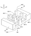
図10は、本発明の第2実施例である変位量モニタ電極100の上面図を示す。尚、図10において、上記図2に示す構成と同一の構成部分については、同一の符号を付してその説明を省略又は簡略する。また、図11は、本実施例の変位量モニタ電極100における動作工程を表した図を示す。
本実施例の変位量モニタ電極100は、固定電極32と可動電極34とからなる。固定電極32は、櫛歯状に形成されており、基部40から半導体基板14に対して平行なX軸方向に延びる電極指102を有している。電極指102は、一つの基部40に対して互いに平行にY軸方向に等間隔で並んで複数本設けられている。各電極指102は、同じ形状を有している。各電極指102はそれぞれ、断面四角状に形成されており、基部40との接続部から先端にかけて断面積が変化するように構成されている。
具体的には、各電極指102はそれぞれ、基部40との接続部近傍及び先端近傍の部位のY軸方向における幅がその中間部位のY軸方向における幅に比べて大きいことで、基部40との接続部近傍及び先端近傍の部位の断面積がその中間部位の断面積に比べて大きくなるように構成されている。以下、電極指102のうち、断面積が比較的大きい基部40との接続部近傍の部位を根元部102-1と、断面積が比較的大きい先端近傍の部位を先端部102-2と、また、断面積が比較的小さい中間部位を中間部102-3と、それぞれ称す。
固定電極32及び可動電極34は、基部40,50同士がX軸方向において対向し、かつ、電極指102と電極指52とがY軸方向において対向して噛み合うように配置されている。具体的には、可動電極34の各電極指52は、固定電極32の互いにY軸方向において隣接する2つの電極指102の中央位置に進入するように配置されている。互いにY軸方向に隣接する可動電極34の電極指52と固定電極32の電極指102とは、部位に応じてY軸方向において異なるギャップ長dmが形成されるように、具体的には、電極指52と根元部102-1との間のギャップ長及び電極指52と先端部102-2との間のギャップ長が比較的小さくかつ電極指52と中間部102-3との間のギャップ長が比較的大きくなるように構成されている。
可動電極34の各電極指52は、構造体16,18の振動中心(すなわち、可動電極34の変位中心)でその先端がX軸方向において固定電極32の電極指102の中間部102-3のX軸方向における中間に位置するように構成されている。また、中間部102-3のX軸方向における長さ、すなわち、根元部102-1と先端部102-2とのX軸方向における距離は、構造体16,18の目標振幅(すなわち、その目標振幅に対応する可動電極34の先端の振動中心からの目標変位量)A0の2倍の値と同一になるように又はその値よりも僅かに小さくなるように設定されている。
尚、Y軸方向において互いに隣接する固定電極32の電極指102と可動電極34の電極指52とが厚さ方向すなわちZ軸方向において重なる部位における厚さ(すなわち電極指102の側壁と電極指52の側壁とがZ軸方向において対向する部位における高さ)Tmは、電極指102のZ軸方向の厚さ又は電極指52のZ軸方向の厚さと異なるものとしてもよく、両厚さと一致するものとしてもよい。
かかる変位量モニタ電極100の構造において、可動電極34が駆動変位量xがゼロである位置(x=0)から駆動変位量xが目標変位量A0である位置(x=A0)まで駆動変位する過程(第1の過程)では、可動電極34と対向する固定電極32のうち固定電極32と可動電極34との対向面積の増加に寄与する電極指102が中間部102-3である。この場合は、その固定電極32の電極指102と可動電極34の電極指52とのY軸方向におけるギャップ長dmが比較的大きい一定値である。このため、上記の第1の過程では、固定電極32と可動電極34との間の静電容量変化量ΔCが一定の傾きで増加する。
また、可動電極34が駆動変位量xが目標変位量A0である位置(x=A0)から更にx>A0側へ駆動変位する過程(第2の過程)では、可動電極34と対向する固定電極32のうち固定電極32と可動電極34との対向面積の増加に寄与する電極指102が根元部102-1となる。この場合は、その固定電極32の電極指102と可動電極34の電極指52とのY軸方向におけるギャップ長dmが比較的小さい一定値となる。このため、上記の第2の過程では、固定電極32と可動電極34との間の静電容量変化量ΔCが、上記の第1の過程での傾きに比べて大きな傾きで増加する。
また、可動電極34がx>A0の位置からx=A0の位置まで駆動変位する過程(第3の過程)では、可動電極34と対向する固定電極32のうち固定電極32と可動電極34との対向面積の減少に寄与する電極指102が根元部102-1である。この場合は、その固定電極32の電極指102と可動電極34の電極指52とのY軸方向におけるギャップ長dmが比較的小さい一定値である。このため、上記の第3の過程では、固定電極32と可動電極34との間の静電容量変化量ΔCが、上記の第2の過程での傾きと同じ傾きで減少する。
また、可動電極34がx=A0の位置からx=0の位置まで駆動変位する過程(第4の過程)、及び、可動電極34がx=0の位置からx=-A0の位置まで駆動変位する過程(第5の過程)では、可動電極34と対向する固定電極32のうち固定電極32と可動電極34との対向面積の減少に寄与する電極指102が中間部102-3となる。この場合は、その固定電極32の電極指102と可動電極34の電極指52とのY軸方向におけるギャップ長dmが比較的大きい一定値となる。このため、上記の第4及び第5の過程では、固定電極32と可動電極34との間の静電容量変化量ΔCが、上記の第3の過程での傾きに比べて小さな傾きで減少する。
また、可動電極34が駆動変位量xが目標変位量-A0である位置(x=-A0)から更にx<-A0側へ駆動変位する過程(第6の過程)では、可動電極34と対向する固定電極32のうち固定電極32と可動電極34との対向面積の減少に寄与する電極指102が先端部102-2となる。この場合は、その固定電極32の電極指102と可動電極34の電極指52とのY軸方向におけるギャップ長dmが比較的小さい一定値となる。このため、上記の第6の過程では、固定電極32と可動電極34との間の静電容量変化量ΔCが、上記の第4及び第5の過程での傾きに比べて大きな傾きで減少する。
また、可動電極34がx<-A0の位置からx=-A0の位置まで駆動変位する過程(第7の過程)では、可動電極34と対向する固定電極32のうち固定電極32と可動電極34との対向面積の増加に寄与する電極指102が先端部102-2である。この場合は、その固定電極32の電極指102と可動電極34の電極指52とのY軸方向におけるギャップ長dmが比較的小さい一定値である。このため、上記の第7の過程では、固定電極32と可動電極34との間の静電容量変化量ΔCが、上記の第6の過程での傾きと同じ傾きで増加する。
更に、可動電極34がx=-A0の位置からx=0の位置まで駆動変位する過程(第8の過程)では、可動電極34と対向する固定電極32のうち固定電極32と可動電極34との対向面積の増加に寄与する電極指102が中間部102-3となる。この場合は、その固定電極32の電極指102と可動電極34の電極指52とのY軸方向におけるギャップ長dmが比較的大きい一定値となる。このため、上記の第8の過程では、固定電極32と可動電極34との間の静電容量変化量ΔCが、上記の第7の過程での傾きに比べて小さな傾きで増加する。
このように、変位量モニタ電極100の構造も、可動電極34の駆動変位量xが目標変位量-A0とA0との間であるときは、可動電極34のX軸方向への駆動変位量xに対する固定電極32と可動電極34との間の静電容量変化量ΔCの変化感度が比較的小さく、一方、可動電極34の駆動変位量xがx<-A0又はx>A0を満たすときは、その変化感度が比較的大きくなる特性を有している。
すなわち、変位量モニタ電極100の構造は、上記した静電容量変化量ΔCの変化感度が、可動電極34の駆動変位が目標変位量A0に達した後はその目標変位量A0に達する前に比べて大きくなり、かつ、可動電極34の駆動変位が目標変位量-A0に達した後はその目標変位量-A0に達する前に比べて大きくなる特性を有している。具体的には、固定電極32及び可動電極34(特に、固定電極32)は、電極指102,52同士が対向するギャップ長dm(特に、電極指52の先端が電極指102に対向するギャップ長)が、可動電極34の駆動変位が目標変位量A0に達した後はその目標変位量A0に達する前に比べて小さくなり、かつ、可動電極34の駆動変位が目標変位量-A0に達した後はその目標変位量-A0に達する前に比べて小さくなるように形成されている。
このため、変位量モニタ電極100の構造においても、可動電極34が目標変位量A0,-A0まで駆動変位した後の可動電極34の駆動変位量xに対する固定電極32と可動電極34との間の静電容量変化量ΔCの変化感度が、可動電極34が目標変位量-A0とA0との間に位置するときのものに比べて高くなる。従って、本実施例の変位量モニタ電極100の構造においても、上記した第1実施例の変位量モニタ電極10の構造と同様の効果を得ることができる。
また、変位量モニタ電極100の構造においては、固定電極32の電極指102の各部と可動電極34の電極指52とがY軸方向において隣接するギャップ長、及び、固定電極32のY軸方向において互いに隣接する電極指102同士の各部がY軸方向において隣接するギャップ長をそれぞれ等間隔とすることができるので、不均一なギャップ長を有する構造に比べて、構成の簡素化及びコンパクト化を図ることができる。
ところで、上記の第2実施例においては、固定電極32及び可動電極34の電極指102,52同士が対向するギャップ長dm(特に、電極指52の先端が電極指102に対向するギャップ長)を、可動電極34の駆動変位が目標変位量A0に達した後はその目標変位量A0に達する前に比べて小さくするうえで、可動電極34の電極指52が基部50との接続部から先端まで同じ断面積を有するものとし、固定電極32の電極指102が基部40との接続部から先端にかけて変化する断面積を有するものとしたが、本発明はこれに限定されるものではなく、固定電極32の電極指及び可動電極34の電極指がそれぞれ、基部との接続部から先端にかけて変化する断面積を有するものとしてもよい。
例えば、図12に示す如く、固定電極32の電極指120が、基部40との接続部近傍の断面積が比較的大きい根元部120-1と、先端近傍の断面積が比較的大きい先端部120-2と、断面積が比較的小さい中間部120-3と、からなるものとし、かつ、可動電極34の電極指122が、基部50との接続部近傍の断面積が比較的大きい根元部122-1と、先端近傍の断面積が比較的大きい先端部122-2と、断面積が比較的小さい中間部122-3と、からなるものとしてもよい。かかる変形例の構造においては、可動電極34の駆動変位が目標変位量A0,-A0に達した後における固定電極32と可動電極34との間の静電容量変化量ΔCの変化感度が、可動電極34の駆動変位がその目標変位量A0,-A0に達する前の変化感度に比べて更に大きくなるので、効果を上記の第2実施例のものに比べて更に顕著なものとすることができる。
また、図13に示す如く、固定電極32の電極指130が、基部40との接続部近傍の断面積が比較的大きい根元部130-1と、断面積が比較的小さい基礎部130-2と、からなるものとし、かつ、可動電極34の電極指132が、基部50との接続部近傍の断面積が比較的大きい根元部132-1と、先端近傍の断面積が比較的大きい先端部132-2と、断面積が比較的小さい中間部132-3と、からなるものとしてもよい。かかる変形例の構造においては、可動電極34の駆動変位が目標変位量A0に達した後における固定電極32と可動電極34との間の静電容量変化量ΔCの変化感度が、可動電極34の駆動変位がその目標変位量A0に達する前の変化感度に比べて更に大きくなるので、効果を上記の第2実施例のものに比べて更に顕著なものとすることができる。
また、図14に示す如く、固定電極32の電極指140が、基部40との接続部近傍の断面積が比較的大きい根元部140-1と、断面積が比較的小さい基礎部140-2と、からなるものとし、かつ、可動電極34の電極指142が、断面積が比較的小さい基礎部142-1と、基部50との接続部近傍の断面積が比較的大きい先端部142-2と、からなるものとしてもよい。かかる変形例の構造においては、可動電極34の駆動変位が目標変位量A0に達した後における固定電極32と可動電極34との間の静電容量変化量ΔCの変化感度が、可動電極34の駆動変位がその目標変位量A0に達する前の変化感度に比べて更に大きくなるので、効果を上記の第2実施例のものに比べて更に顕著なものとすることができる。
また、上記した図12~図14に示す変形例の構造においては、図15(尚、この図15には、図13に示す変形例の構造を示している。)に示す如く、変位量モニタ電極100全体の構成として、固定電極32の電極指と可動電極34の電極指とがY軸方向において対向する部位ごとのギャップ長、及び、固定電極32のY軸方向において互いに隣接する電極指同士の部位ごとのギャップ長をそれぞれ等間隔とすること(すなわち、図15に示す如く、a=a´=a´´=a´´´、b=b´=b´´=b´´´、c=c´、かつ、d=d´を成立させること)ができるので、不均一なギャップ長を有する構造に比べて、構成の簡素化及びコンパクト化を図ることができる。
図16は、本発明の第3実施例である変位量モニタ電極200の上面図を示す。尚、図10において、上記図2に示す構成と同一の構成部分については、同一の符号を付してその説明を省略又は簡略する。また、図17は、本実施例の変位量モニタ電極200における動作工程を表した図を示す。
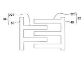
本実施例の変位量モニタ電極200は、固定電極32と可動電極34とからなる。固定電極32は、櫛歯状に形成されており、基部40から半導体基板14に対して平行なX軸方向に延びる電極指202を有している。電極指202は、一つの基部40に対して互いに平行にY軸方向に等間隔で並んで複数本設けられている。各電極指202は、同じ形状を有している。各電極指202はそれぞれ、断面四角状に形成されており、基部40との接続部から先端にかけて断面積が変化するように構成されている。
具体的には、各電極指202はそれぞれ、基部40との接続部近傍及び先端近傍の部位のZ軸方向における厚さがその中間部位のZ軸方向における厚さに比べて大きいことで、基部40との接続部近傍及び先端近傍の部位の断面積がその中間部位の断面積に比べて大きくなるように構成されている。以下、電極指202のうち、断面積が比較的大きい基部40との接続部近傍の部位を根元部202-1と、断面積が比較的大きい先端近傍の部位を先端部202-2と、また、断面積が比較的小さい中間部位を中間部202-3と、それぞれ称す。
固定電極32及び可動電極34は、基部40,50同士がX軸方向において対向し、かつ、電極指202と電極指52とがY軸方向において対向して噛み合うように配置されている。具体的には、可動電極34の各電極指52は、固定電極32の互いにY軸方向において隣接する2つの電極指202の中央位置に進入するように配置されている。互いにY軸方向に隣接する可動電極34の電極指52と固定電極32の電極指202との間には、Y軸方向において所定のギャップ長d0が形成されている。
可動電極34の各電極指52は、構造体16,18の振動中心(すなわち、可動電極34の変位中心)でその先端がX軸方向において固定電極32の電極指202の中間部202-3のX軸方向における中間に位置するように構成されている。また、中間部202-3のX軸方向における長さ、すなわち、根元部202-1と先端部202-2とのX軸方向における距離は、構造体16,18の目標振幅(すなわち、その目標振幅に対応する可動電極34の先端の振動中心からの目標変位量)A0の2倍の値と同一になるように又はその値よりも僅かに小さくなるように設定されている。
また、Y軸方向において互いに隣接する固定電極32の電極指202と可動電極34の電極指52とは、厚さ方向すなわちZ軸方向において重なる部位における厚さ(すなわち電極指202の側壁と電極指52の側壁とがZ軸方向において対向する部位における高さ)Tmが部位に応じて異なるように、具体的には、電極指52と根元部202-1との間の厚さ及び電極指52と先端部202-2との間の厚さが比較的大きくかつ電極指52と中間部202-3との間の厚さが比較的小さくなるように構成されている。
かかる変位量モニタ電極200の構造において、可動電極34が駆動変位量xがゼロである位置(x=0)から駆動変位量xが目標変位量A0である位置(x=A0)まで駆動変位する過程(第1の過程)では、可動電極34と対向する固定電極32のうち固定電極32と可動電極34との対向面積の増加に寄与する電極指202が中間部202-3である。この場合は、その固定電極32の電極指202と可動電極34の電極指52とがY軸方向において対向するZ軸方向の高さTmが比較的小さい一定値であり、固定電極32と可動電極34とがギャップ長d0だけ隔てて対向する面積がその可動電極34の変位に従って比例的に増加する。このため、上記の第1の過程では、固定電極32と可動電極34との間の静電容量変化量ΔCが一定の傾きで増加する。
また、可動電極34が駆動変位量xが目標変位量A0である位置(x=A0)から更にx>A0側へ駆動変位する過程(第2の過程)では、可動電極34と対向する固定電極32のうち固定電極32と可動電極34との対向面積の増加に寄与する電極指202が根元部202-1となる。この場合は、その固定電極32の電極指202と可動電極34の電極指52とがY軸方向において対向するZ軸方向の高さTmが比較的大きい一定値となり、固定電極32と可動電極34とがギャップ長d0だけ隔てて対向する面積がその可動電極34の変位に従って比例的に増加すると共に、その面積の増加傾きが、上記した第1の過程での増加傾きよりも大きくなる。このため、上記の第2の過程では、固定電極32と可動電極34との間の静電容量変化量ΔCが、上記の第1の過程での傾きに比べて大きな傾きで増加する。
また、可動電極34がx>A0の位置からx=A0の位置まで駆動変位する過程(第3の過程)では、可動電極34と対向する固定電極32のうち固定電極32と可動電極34との対向面積の減少に寄与する電極指202が根元部202-1である。この場合は、その固定電極32の電極指202と可動電極34の電極指52とがY軸方向において対向するZ軸方向の高さTmが比較的大きい一定値であり、固定電極32と可動電極34とがギャップ長d0だけ隔てて対向する面積がその可動電極34の変位に従って比例的に減少する。このため、上記の第3の過程では、固定電極32と可動電極34との間の静電容量変化量ΔCが、上記の第2の過程での傾きと同じ傾きで減少する。
また、可動電極34がx=A0の位置からx=0の位置まで駆動変位する過程(第4の過程)、及び、可動電極34がx=0の位置からx=-A0の位置まで駆動変位する過程(第5の過程)では、可動電極34と対向する固定電極32のうち固定電極32と可動電極34との対向面積の減少に寄与する電極指202が中間部202-3となる。この場合は、その固定電極32の電極指202と可動電極34の電極指52とがY軸方向において対向するZ軸方向の高さTmが比較的小さい一定値となり、固定電極32と可動電極34とがギャップ長d0だけ隔てて対向する面積がその可動電極34の変位に従って比例的に減少すると共に、その面積の減少傾きが、上記の第3の過程での減少傾きよりも小さくなる。このため、上記の第4及び第5の過程では、固定電極32と可動電極34との間の静電容量変化量ΔCが、上記の第3の過程での傾きに比べて小さな傾きで減少する。
また、可動電極34が駆動変位量xが目標変位量-A0である位置(x=-A0)から更にx<-A0側へ駆動変位する過程(第6の過程)では、可動電極34と対向する固定電極32のうち固定電極32と可動電極34との対向面積の減少に寄与する電極指202が先端部202-2となる。この場合は、その固定電極32の電極指202と可動電極34の電極指52とがY軸方向において対向するZ軸方向の高さTmが比較的大きい一定値となり、固定電極32と可動電極34とがギャップ長d0だけ隔てて対向する面積がその可動電極34の変位に従って比例的に減少すると共に、その面積の減少傾きが、上記した第4及び第5の過程での減少傾きよりも大きくなる。このため、上記の第6の過程では、固定電極32と可動電極34との間の静電容量変化量ΔCが、上記の第4及び第5の過程での傾きに比べて大きな傾きで減少する。
また、可動電極34がx<-A0の位置からx=-A0の位置まで駆動変位する過程(第7の過程)では、可動電極34と対向する固定電極32のうち固定電極32と可動電極34との対向面積の増加に寄与する電極指202が先端部202-2である。この場合は、その固定電極32の電極指202と可動電極34の電極指52とがY軸方向において対向するZ軸方向の高さTmが比較的大きい一定値であり、固定電極32と可動電極34とがギャップ長d0だけ隔てて対向する面積がその可動電極34の変位に従って比例的に増加する。このため、上記の第7の過程では、固定電極32と可動電極34との間の静電容量変化量ΔCが、上記の第6の過程での傾きと同じ傾きで増加する。
更に、可動電極34がx=-A0の位置からx=0の位置まで駆動変位する過程(第8の過程)では、可動電極34と対向する固定電極32のうち固定電極32と可動電極34との対向面積の増加に寄与する電極指202が中間部202-3となる。この場合は、その固定電極32の電極指202と可動電極34の電極指52とがY軸方向において対向するZ軸方向の高さTmが比較的小さい一定値となり、固定電極32と可動電極34とがギャップ長d0だけ隔てて対向する面積がその可動電極34の変位に従って比例的に増加すると共に、その面積の増加傾きが、上記の第7の過程での増加傾きよりも小さくなる。このため、上記の第8の過程では、固定電極32と可動電極34との間の静電容量変化量ΔCが、上記の第7の過程での傾きに比べて小さな傾きで増加する。
このように、変位量モニタ電極200の構造も、可動電極34の駆動変位量xが目標変位量-A0とA0との間であるときは、可動電極34のX軸方向への駆動変位量xに対する固定電極32と可動電極34との間の静電容量変化量ΔCの変化感度が比較的小さく、一方、可動電極34の駆動変位量xがx<-A0又はx>A0を満たすときは、その変化感度が比較的大きくなる特性を有している。
すなわち、変位量モニタ電極200の構造は、上記した静電容量変化量ΔCの変化感度が、可動電極34の駆動変位が目標変位量A0に達した後はその目標変位量A0に達する前に比べて大きくなり、かつ、可動電極34の駆動変位が目標変位量-A0に達した後はその目標変位量-A0に達する前に比べて大きくなる特性を有している。具体的には、固定電極32及び可動電極34(特に、固定電極32)は、電極指202,52同士がY軸方向において対向するZ軸方向の高さTm(特に、電極指52の先端が電極指202に対向するZ軸方向の高さ)が、可動電極34の駆動変位が目標変位量A0に達した後はその目標変位量A0に達する前に比べて大きくなり、かつ、可動電極34の駆動変位が目標変位量-A0に達した後はその目標変位量-A0に達する前に比べて大きくなるように形成されている。
このため、変位量モニタ電極200の構造においても、可動電極34が目標変位量A0,-A0まで駆動変位した後の可動電極34の駆動変位量xに対する固定電極32と可動電極34との間の静電容量変化量ΔCの変化感度が、可動電極34が目標変位量-A0とA0との間に位置するときのものに比べて高くなる。従って、本実施例の変位量モニタ電極200の構造においても、上記した第1実施例及び第2実施例の変位量モニタ電極10,100の構造と同様の効果を得ることができる。
また、変位量モニタ電極200の構造においては、上記した第1実施例及び第2実施例の変位量モニタ電極10,100の構造と異なり、固定電極32の電極指202及び可動電極34の電極指52がそれぞれ、先端から基部40,50との接続部にかけてY軸方向の幅が変化しない構成を有する。このため、固定電極32の電極指202と可動電極34の電極指52とがY軸方向において対向するギャップ長、固定電極32のY軸方向において互いに隣接する電極指202同士がY軸方向において隣接するギャップ長、及び可動電極34のY軸方向において互いに隣接する電極指52同士がY軸方向において隣接するギャップ長をそれぞれ最短でかつ等間隔とすることができるので、不均一なギャップ長を有する構造に比べて、構成の簡素化及びコンパクト化を図ることができ、半導体基板14上において変位量モニタ電極200が占有する面積が増大するのを防止することができる。
ところで、上記の第3実施例においては、固定電極32及び可動電極34の電極指202,52同士がY軸方向において対向するZ軸方向の高さTm(特に、電極指52の先端が電極指202に対向するZ軸方向の高さ)を、可動電極34の駆動変位が目標変位量A0に達した後はその目標変位量A0に達する前に比べて小さくするうえで、可動電極34の電極指52が基部50との接続部から先端まで同じ断面積を有するものとし、固定電極32の電極指202が基部40との接続部から先端にかけて変化する断面積を有するものとしたが、本発明はこれに限定されるものではなく、固定電極32の電極指及び可動電極34の電極指がそれぞれ、基部との接続部から先端にかけて変化する断面積を有するものとしてもよい。
例えば、図18A、図18B、及び図18Cに示す如く、固定電極32の電極指220が、基部40との接続部近傍の断面積が比較的大きい根元部220-1と、先端近傍の断面積が比較的大きい先端部220-2と、断面積が比較的小さい中間部220-3と、からなるものとし、かつ、可動電極34の電極指222が、基部50との接続部近傍の断面積が比較的大きい根元部222-1と、先端近傍の断面積が比較的大きい先端部222-2と、断面積が比較的小さい中間部222-3と、からなるものとしてもよい。かかる変形例の構造においては、可動電極34の駆動変位が目標変位量A0,-A0に達した後における固定電極32と可動電極34との間の静電容量変化量ΔCの変化感度が、可動電極34の駆動変位がその目標変位量A0,-A0に達する前の変化感度に比べて更に大きくなるので、効果を上記の第3実施例のものに比べて更に顕著なものとすることができる。
また、図19A、図19B、及び図19Cに示す如く、固定電極32の電極指230が、基部40との接続部近傍の断面積が比較的大きい根元部230-1と、断面積が比較的小さい基礎部230-2と、からなるものとし、かつ、可動電極34の電極指232が、基部50との接続部近傍の断面積が比較的大きい根元部232-1と、先端近傍の断面積が比較的大きい先端部232-2と、断面積が比較的小さい中間部232-3と、からなるものとしてもよい。かかる変形例の構造においては、可動電極34の駆動変位が目標変位量A0に達した後における固定電極32と可動電極34との間の静電容量変化量ΔCの変化感度が、可動電極34の駆動変位がその目標変位量A0に達する前の変化感度に比べて更に大きくなるので、効果を上記の第3実施例のものに比べて更に顕著なものとすることができる。
また、図20A、図20B、及び図20Cに示す如く、固定電極32の電極指240が、基部40との接続部近傍の断面積が比較的大きい根元部240-1と、断面積が比較的小さい基礎部240-2と、からなるものとし、かつ、可動電極34の電極指242が、断面積が比較的小さい基礎部242-1と、基部50との接続部近傍の断面積が比較的大きい先端部242-2と、からなるものとしてもよい。かかる変形例の構造においては、可動電極34の駆動変位が目標変位量A0に達した後における固定電極32と可動電極34との間の静電容量変化量ΔCの変化感度が、可動電極34の駆動変位がその目標変位量A0に達する前の変化感度に比べて更に大きくなるので、効果を上記の第3実施例のものに比べて更に顕著なものとすることができる。
また、上記した図18~図20に示す変形例の構造においても、変位量モニタ電極200全体の構成として、固定電極32の電極指と可動電極34の電極指とがY軸方向において対向するギャップ長、固定電極32のY軸方向において互いに隣接する電極指同士がY軸方向において隣接するギャップ長、及び可動電極34のY軸方向において互いに隣接する電極指同士がY軸方向において隣接するギャップ長をそれぞれ最短でかつ等間隔とすること(例えば、図21に示す如く、e=e´=e´´=e´´´を成立させること)ができるので、不均一なギャップ長を有する構造に比べて、構成の簡素化及びコンパクト化を図ることができ、半導体基板14上において変位量モニタ電極200が占有する面積が増大するのを防止することができる。
図22Aは、本発明の第4実施例である変位量モニタ電極300の上面図を示す。図22Bは、図22Aに示す変位量モニタ電極300のV-V断面図を示す。尚、図22A及び図22Bにおいて、上記図2に示す構成と同一の構成部分については、同一の符号を付してその説明を省略又は簡略する。また、図23は、本実施例の変位量モニタ電極300における動作工程を表した図を示す。
本実施例の変位量モニタ電極300は、固定電極32と可動電極34とからなる。固定電極32は、櫛歯状に形成されており、基部40から半導体基板14に対して平行なX軸方向に延びる電極指302を有している。電極指302は、一つの基部40に対して互いに平行にY軸方向に等間隔で並んで複数本設けられている。各電極指302は、互いに同じ形状を有している。電極指302は、断面四角状に形成されており、基部40との接続部から先端まで同じ断面積(Y軸方向において同じ幅かつZ軸方向において同じ厚さ)を有している。また、電極指302と可動電極34の電極指52とが厚さ方向すなわちZ軸方向において重なる部位における厚さ(すなわち電極指302の側壁と電極指52の側壁とがZ軸方向において対向する部位における高さ)Tmは一定である。
固定電極32の電極指302において、基部40との接続部近傍及び先端近傍の部位の表面には、誘電材料304,306が配設されている。誘電材料304,306は、電極指302が可動電極34の電極指52とY軸方向において対向する側面の両側それぞれに設けられている。誘電材料304,306は、電極指302本体の材料とは異なる、絶縁性の高い材料又は低ヤング率若しくは粘性を有する材料により構成されている。誘電材料304,306は、空気の比誘電率“1”よりも大きい比誘電率を有しており、電極指302の表面上においてY軸方向に所定厚さd1を有している。
尚、誘電材料304,306は、例えばシリコンを熱酸化することで容易に堆積可能なSiO2膜(酸化絶縁膜)やレジスト材料などの有機材料などを利用して製造されるものとしてもよい。また、以下、電極指302のうち、誘電材料304が設けられた基部40との接続部近傍の部位を根元部302-1と、誘電材料306が設けられた先端近傍の部位を先端部302-2と、また、根元部302-1と先端部302-2との中間部位を中間部302-3と、それぞれ称す。
固定電極32及び可動電極34は、基部40,50同士がX軸方向において対向し、かつ、電極指302と電極指52とがY軸方向において対向して噛み合うように配置されている。具体的には、可動電極34の各電極指52は、固定電極32の互いにY軸方向において隣接する2つの電極指302の中央位置に進入するように配置されている。互いにY軸方向に隣接する可動電極34の電極指52と固定電極32の電極指302との間には、電極指302の中間部302-3でY軸方向に所定のギャップ長d0が、また、根元部302-1及び先端部302-2でY軸方向に所定のギャップ長(d0-d1)が、それぞれ形成されている。
可動電極34の各電極指52は、構造体16,18の振動中心(すなわち、可動電極34の変位中心)でその先端がX軸方向において固定電極32の電極指302の中間部302-3のX軸方向における中間に位置するように構成されている。また、中間部302-3のX軸方向における長さ、すなわち、根元部302-1と先端部302-2とのX軸方向における距離(誘電材料304の一端と誘電材料306の一端とのX軸方向における離間距離)は、構造体16,18の目標振幅(すなわち、その目標振幅に対応する可動電極34の先端の振動中心からの目標変位量)A0の2倍の値と同一になるように又はその値よりも僅かに小さくなるように設定されている。
尚、Y軸方向において互いに隣接する固定電極32の電極指302と可動電極34の電極指52とが厚さ方向すなわちZ軸方向において重なる部位における厚さ(すなわち電極指302の側壁と電極指52の側壁とがZ軸方向において対向する部位における高さ)Tmは、電極指102のZ軸方向の厚さ又は電極指52のZ軸方向の厚さと異なるものとしてもよく、両厚さと一致するものとしてもよい。
かかる変位量モニタ電極300の構造において、可動電極34が駆動変位量xがゼロである位置(x=0)から駆動変位量xが目標変位量A0である位置(x=A0)まで駆動変位する過程(第1の過程)では、可動電極34と対向する固定電極32のうち固定電極32と可動電極34との対向面積の増加に寄与する電極指302が中間部302-3である。このため、上記の第1の過程では、その固定電極32の電極指302と可動電極34の電極指52とのY軸方向における間の誘電率がその間の空間の誘電率に基づく一定値(=ε1)であるので、固定電極32と可動電極34との間の静電容量変化量ΔC1が次式(2)に示す如く上記の駆動変位量xに従って一定の傾きで増加する。尚、固定電極32と可動電極34とが対向する対向面積の変化量をΔSとする。
ΔC1=ε1・ΔS/d0 ・・・(2)
また、可動電極34が駆動変位量xが目標変位量A0である位置(x=A0)から更にx>A0側へ駆動変位する過程(第2の過程)では、可動電極34と対向する固定電極32のうち固定電極32と可動電極34との対向面積の増加に寄与する電極指302が根元部302-1となる。このため、上記の第2の過程では、固定電極32と可動電極34との間の静電容量変化量ΔC2が、次式(3)に示す如く、誘電材料304の静電容量変化量と、その誘電材料304と可動電極34の電極指52とのY軸方向における間の空間の静電容量変化量と、に基づくものとなり、上記の駆動変位量xに従って上記の第1の過程での傾きに比べて大きな傾きで増加する。尚、固定電極32の電極指302と可動電極34の電極指52との間の空間の誘電率をε1とし、誘電材料304の誘電率をε2(>ε1)とし、固定電極32と可動電極34と対向面積の変化量をΔSとする。
また、可動電極34が駆動変位量xが目標変位量A0である位置(x=A0)から更にx>A0側へ駆動変位する過程(第2の過程)では、可動電極34と対向する固定電極32のうち固定電極32と可動電極34との対向面積の増加に寄与する電極指302が根元部302-1となる。このため、上記の第2の過程では、固定電極32と可動電極34との間の静電容量変化量ΔC2が、次式(3)に示す如く、誘電材料304の静電容量変化量と、その誘電材料304と可動電極34の電極指52とのY軸方向における間の空間の静電容量変化量と、に基づくものとなり、上記の駆動変位量xに従って上記の第1の過程での傾きに比べて大きな傾きで増加する。尚、固定電極32の電極指302と可動電極34の電極指52との間の空間の誘電率をε1とし、誘電材料304の誘電率をε2(>ε1)とし、固定電極32と可動電極34と対向面積の変化量をΔSとする。
ΔC2=ε1・ε2・ΔS/(ε2・(d0-d1)+ε1・d1) ・・・(3)
また、可動電極34がx>A0の位置からx=A0の位置まで駆動変位する過程(第3の過程)では、可動電極34と対向する固定電極32のうち固定電極32と可動電極34との対向面積の減少に寄与する電極指302が根元部302-1である。このため、上記の第3の過程では、固定電極32と可動電極34との間の静電容量変化量ΔCが、上記の駆動変位量xに従って上記の第2の過程での傾きと同じ傾きで減少する。
また、可動電極34がx>A0の位置からx=A0の位置まで駆動変位する過程(第3の過程)では、可動電極34と対向する固定電極32のうち固定電極32と可動電極34との対向面積の減少に寄与する電極指302が根元部302-1である。このため、上記の第3の過程では、固定電極32と可動電極34との間の静電容量変化量ΔCが、上記の駆動変位量xに従って上記の第2の過程での傾きと同じ傾きで減少する。
また、可動電極34がx=A0の位置からx=0の位置まで駆動変位する過程(第4の過程)、及び、可動電極34がx=0の位置からx=-A0の位置まで駆動変位する過程(第5の過程)では、可動電極34と対向する固定電極32のうち固定電極32と可動電極34との対向面積の減少に寄与する電極指302が中間部302-3となる。このため、上記の第4及び第5の過程では、固定電極32と可動電極34との間の静電容量変化量ΔCが、上記の駆動変位量xに従って上記の第3の過程での傾きに比べて小さな傾きで減少する。
また、可動電極34が駆動変位量xが目標変位量-A0である位置(x=-A0)から更にx<-A0側へ駆動変位する過程(第6の過程)では、可動電極34と対向する固定電極32のうち固定電極32と可動電極34との対向面積の減少に寄与する電極指302が先端部302-2となる。このため、上記の第6の過程では、固定電極32と可動電極34との間の静電容量変化量ΔCが、誘電材料306の静電容量変化量と、その誘電材料306と可動電極34の電極指52との間の空間の静電容量変化量と、に基づくものとなり、上記の駆動変位量xに従って上記の第4及び第5の過程での傾きに比べて大きな傾きで減少する。
また、可動電極34がx<-A0の位置からx=-A0の位置まで駆動変位する過程(第7の過程)では、可動電極34と対向する固定電極32のうち固定電極32と可動電極34との対向面積の増加に寄与する電極指302が先端部302-2である。このため、上記の第7の過程では、固定電極32と可動電極34との間の静電容量変化量ΔCが、上記の駆動変位量xに従って上記の第6の過程での傾きと同じ傾きで増加する。
更に、可動電極34がx=-A0の位置からx=0の位置まで駆動変位する過程(第8の過程)では、可動電極34と対向する固定電極32のうち固定電極32と可動電極34との対向面積の増加に寄与する電極指302が中間部302-3となる。このため、上記の第8の過程では、固定電極32と可動電極34との間の静電容量変化量ΔCが、上記の駆動変位量xに従って上記の第7の過程での傾きに比べて小さな傾きで増加する。
このように、変位量モニタ電極300の構造も、可動電極34の駆動変位量xが目標変位量-A0とA0との間であるときは、可動電極34のX軸方向への駆動変位量xに対する固定電極32と可動電極34との間の静電容量変化量ΔCの変化感度が比較的小さく、一方、可動電極34の駆動変位量xがx<-A0又はx>A0を満たすときは、その変化感度が比較的大きくなる特性を有している。
すなわち、変位量モニタ電極300の構造は、上記した静電容量変化量ΔCの変化感度が、可動電極34の駆動変位が目標変位量A0に達した後はその目標変位量A0に達する前に比べて大きくなり、かつ、可動電極34の駆動変位が目標変位量-A0に達した後はその目標変位量-A0に達する前に比べて大きくなる特性を有している。具体的には、固定電極32及び可動電極34(特に、固定電極32)は、上記した静電容量変化量ΔCの変化感度が上記した特性を有するように、先端近傍や基部との接続部近傍に誘電材料304,306が配設された電極指を有している。
このため、変位量モニタ電極300の構造においても、可動電極34が目標変位量A0,-A0まで駆動変位した後の可動電極34の駆動変位量xに対する固定電極32と可動電極34との間の静電容量変化量ΔCの変化感度が、可動電極34が目標変位量-A0とA0との間に位置するときのものに比べて高くなる。従って、本実施例の変位量モニタ電極300の構造においても、上記した第1実施例~第3実施例の変位量モニタ電極10,100,200の構造と同様の効果を得ることができる。
また、変位量モニタ電極300において、誘電材料304,306がそれぞれ絶縁性の高い材料により構成されている場合は、構造体16,18がX軸方向に振動する過程で、製造バラツキや制御バラツキ,外部からの過大応力印加などに起因して可動電極34が固定電極32に衝突しても、その誘電材料304,306の存在により両電極32,34が導通することは回避されるので、固定電極32と可動電極34との間の静電容量の変化を精度よく検出することができ、構造体16,18を半導体基板14に対してX軸方向へ励振駆動させるうえでの誤動作を防止することができる。
更に、変位量モニタ電極300において、誘電材料304,306がそれぞれ低ヤング率若しくは粘性を有する材料により構成されている場合は、製造バラツキや制御バラツキ,外部からの過大応力印加などに起因して可動電極34が固定電極32に衝突しても、誘電材料304,306の存在により両電極32,34に加わる衝撃は吸収されるので、固定電極32及び可動電極34の破損を防止することができる。
ところで、上記の第4実施例においては、固定電極32の電極指302にのみ誘電材料304,306を配設することとしたが、本発明はこれに限定されるものではなく、更に可動電極34の電極指にも誘電材料を配設することとしてもよい。
例えば、図24に示す如く、固定電極32及び可動電極34の電極指320,322の双方それぞれにおいて、基部40,50との接続部近傍及び先端近傍の部位に、誘電材料324,326,328,330を配設することとしてもよい。かかる変形例の構造においては、可動電極34の駆動変位が目標変位量A0,-A0に達した後における固定電極32と可動電極34との間の静電容量変化量ΔCの変化感度が、可動電極34の駆動変位がその目標変位量A0,-A0に達する前の変化感度に比べて更に大きくなるので、効果を上記の第4実施例のものに比べて更に顕著なものとすることができる。
また、図25に示す如く、固定電極32の電極指340において、基部40との接続部近傍の部位にのみ誘電材料342を配設し、かつ、可動電極34の電極指344において、基部50との接続部近傍及び先端近傍の部位に誘電材料346,348を配設することとしてもよい。かかる変形例の構造においては、可動電極34の駆動変位が目標変位量A0,-A0に達した後における固定電極32と可動電極34との間の静電容量変化量ΔCの変化感度が、可動電極34の駆動変位がその目標変位量A0,-A0に達する前の変化感度に比べて更に大きくなるので、効果を上記の第4実施例のものに比べて更に顕著なものとすることができる。
また、図26に示す如く、固定電極32の電極指360において、基部40との接続部近傍の部位にのみ誘電材料362を配設し、かつ、可動電極34の電極指364において、先端近傍の部位にのみ誘電材料366を配設することとしてもよい。かかる変形例の構造においては、可動電極34の駆動変位が目標変位量A0に達した後における固定電極32と可動電極34との間の静電容量変化量ΔCの変化感度が、可動電極34の駆動変位がその目標変位量A0に達する前の変化感度に比べて更に大きくなるので、効果を上記の第4実施例のものに比べて更に顕著なものとすることができる。
また、上記した図24~図26に示す変形例の構造においても、図27に示す如く、固定電極32及び可動電極34に配設した誘電材料の存在により、両電極32,34が導通することが回避されると共に、両電極32,34が衝突したときの衝撃が吸収されるので、上記の第4実施例と同様の効果を得ることができる。
また、上記の第4実施例においては、固定電極32の表面に所定厚さd1の誘電材料304,306を配設することにより、固定電極32の電極指302と可動電極34の電極指52との間の誘電率を変化させて、固定電極32と可動電極34との間の静電容量変化量ΔCの変化感度を可動電極34の駆動変位量に応じて変化させることとしているが、本発明はこれに限定されるものではない。すなわち、固定電極32の電極指302及び可動電極34の電極指52がそれぞれ、先端から基部40,50との接続部にかけてY軸方向の幅が変化しない構成を有するものとし、固定電極32の電極指302の表面と可動電極34の電極指52の表面との間に満たす誘電材料を先端から基部40,50との接続部にかけて異ならせることで、その間の誘電率を変化させて、上記の変化感度を実現させることとしてもよい。例えば、固定電極32の電極指302の表面と可動電極34の電極指52の表面との間に満たす誘電材料を、固定電極32の電極指302の根元部302-1及び先端部302-2に対応する部位では誘電率の比較的高いものとし、一方、その電極指302の中間部302-3に対応する部位では誘電率の比較的低いものとする。
かかる変形例においては、電極指302,52同士がY軸方向において対向する間の誘電率が、可動電極34の駆動変位が目標変位量A0に達した後はその目標変位量A0に達する前に比べて大きくなり、かつ、可動電極34の駆動変位が目標変位量-A0に達した後はその目標変位量-A0に達する前に比べて大きくなる。このため、かかる変形例においても、可動電極34が目標変位量A0,-A0まで駆動変位した後の可動電極34の駆動変位量xに対する固定電極32と可動電極34との間の静電容量変化量ΔCの変化感度が、可動電極34が目標変位量-A0とA0との間に位置するときのものに比べて高くなるので、上記の第4実施例と同様の効果を得ることができる。
また、かかる変形例の構造においては、上記した第1実施例、第2実施例、及び第4実施例の変位量モニタ電極10,100,300の構造と異なり、固定電極32の電極指302及び可動電極34の電極指52がそれぞれ、先端から基部40,50との接続部にかけてY軸方向の幅が変化しない構成を有することとなる。このため、固定電極32の電極指302と可動電極34の電極指52とがY軸方向において対向するギャップ長、固定電極32のY軸方向において互いに隣接する電極指302同士がY軸方向において隣接するギャップ長、及び可動電極34のY軸方向において互いに隣接する電極指52同士がY軸方向において隣接するギャップ長をそれぞれ最短でかつ等間隔とすることができるので、不均一なギャップ長を有する構造に比べて、構成の簡素化及びコンパクト化を図ることができ、半導体基板14上において変位量モニタ電極300が占有する面積が増大するのを防止することができる。
更に、上記の第1~第4実施例においては、変位量モニタ電極10,100,200,300を、角速度を検出するための角速度センサ12に搭載するものとしたが、本発明はこれに限定されるものではなく、構造体の駆動変位量をモニタするものであれば他のセンサに搭載することとしてもよい。
10,28-1,28-2,30-1,30-2,100,200,300 変位量モニタ電極
14 半導体基板
16,18 構造体
32 固定電極
34 可動電極
40,50 基部
42,52,80,90,102,120,122,130,132,140,142,202,220,222,230,232,240,242,302,320,322,340,344,360,364 電極指
304,306,324~330,342,346,348,362,366 誘電材料
14 半導体基板
16,18 構造体
32 固定電極
34 可動電極
40,50 基部
42,52,80,90,102,120,122,130,132,140,142,202,220,222,230,232,240,242,302,320,322,340,344,360,364 電極指
304,306,324~330,342,346,348,362,366 誘電材料
Claims (7)
- それぞれ基部及び該基部から基板に対して平行な所定軸方向に延びる電極指からなる櫛歯状の、前記基板に対して固定される固定電極と、前記所定軸方向に変位し得る可動電極と、が互いの前記電極指同士が噛み合うように対向配置され、前記固定電極と前記可動電極との間の静電容量の変化量に基づいて目標振幅で駆動させるべき検出マスの変位量をモニタする変位量モニタ電極の構造であって、
前記可動電極の前記所定軸方向への変位量に対する前記静電容量の変化量の変化感度は、該可動電極の該所定軸方向への変位が前記目標振幅に対応する目標変位量に達した後は該目標変位量に達する前に比べて大きくなる特性を有することを特徴とする変位量モニタ電極の構造。 - 前記可動電極の中立位置から前記所定軸方向の一方への変位量に対する前記静電容量の変化量の変化感度、及び、前記可動電極の中立位置から前記所定軸方向の他方への変位量に対する前記静電容量の変化量の変化感度はそれぞれ、前記特性を有することを特徴とする請求項1記載の変位量モニタ電極の構造。
- 前記固定電極及び前記可動電極の少なくとも一方は、前記固定電極及び前記可動電極の前記電極指同士が所定距離で対向する面の総面積の変化感度が、該可動電極の前記所定軸方向への変位が前記目標変位量に達した後は該目標変位量に達する前に比べて大きくなるように形成されていることを特徴とする請求項1又は2記載の変位量モニタ電極の構造。
- 前記固定電極及び前記可動電極は、前記固定電極及び前記可動電極の前記電極指同士が所定距離で対向する箇所の個数が、該可動電極の前記所定軸方向への変位が前記目標変位量に達した後は該目標変位量に達する前に比べて増えるように形成されていることを特徴とする請求項3記載の変位量モニタ電極の構造。
- 前記固定電極及び前記可動電極の少なくとも一方は、前記固定電極及び前記可動電極の前記電極指同士が所定距離で対向する面の前記基板に対して垂直な方向の長さが、該可動電極の前記所定軸方向への変位が前記目標変位量に達した後は該目標変位量に達する前に比べて大きくなるように形成されていることを特徴とする請求項3記載の変位量モニタ電極の構造。
- 前記固定電極及び前記可動電極の少なくとも一方は、前記固定電極及び前記可動電極の前記電極指同士が対向するギャップ長が、該可動電極の前記所定軸方向への変位が前記目標変位量に達した後は該目標変位量に達する前に比べて小さくなるように形成されていることを特徴とする請求項1又は2記載の変位量モニタ電極の構造。
- 前記固定電極及び前記可動電極の少なくとも一方は、前記固定電極及び前記可動電極の前記電極指同士が所定距離で対向する間の誘電率が、該可動電極の前記所定軸方向への変位が前記目標変位量に達した後は該目標変位量に達する前に比べて大きくなるように構成されていることを特徴とする請求項1又は2記載の変位量モニタ電極の構造。
Priority Applications (4)
| Application Number | Priority Date | Filing Date | Title |
|---|---|---|---|
| PCT/JP2011/068177 WO2013021467A1 (ja) | 2011-08-09 | 2011-08-09 | 変位量モニタ電極の構造 |
| EP11870767.8A EP2743639B1 (en) | 2011-08-09 | 2011-08-09 | Structure of displacement monitoring electrode |
| CN201180072685.5A CN103717997B (zh) | 2011-08-09 | 2011-08-09 | 位移量监视电极的构造 |
| US14/236,966 US9239222B2 (en) | 2011-08-09 | 2011-08-09 | Displacement amount monitoring electrode structure |
Applications Claiming Priority (1)
| Application Number | Priority Date | Filing Date | Title |
|---|---|---|---|
| PCT/JP2011/068177 WO2013021467A1 (ja) | 2011-08-09 | 2011-08-09 | 変位量モニタ電極の構造 |
Publications (1)
| Publication Number | Publication Date |
|---|---|
| WO2013021467A1 true WO2013021467A1 (ja) | 2013-02-14 |
Family
ID=47668019
Family Applications (1)
| Application Number | Title | Priority Date | Filing Date |
|---|---|---|---|
| PCT/JP2011/068177 WO2013021467A1 (ja) | 2011-08-09 | 2011-08-09 | 変位量モニタ電極の構造 |
Country Status (4)
| Country | Link |
|---|---|
| US (1) | US9239222B2 (ja) |
| EP (1) | EP2743639B1 (ja) |
| CN (1) | CN103717997B (ja) |
| WO (1) | WO2013021467A1 (ja) |
Cited By (3)
| Publication number | Priority date | Publication date | Assignee | Title |
|---|---|---|---|---|
| JP2016099208A (ja) * | 2014-11-20 | 2016-05-30 | セイコーエプソン株式会社 | ジャイロセンサー、電子機器および移動体 |
| JP2016099206A (ja) * | 2014-11-20 | 2016-05-30 | セイコーエプソン株式会社 | ジャイロセンサー、電子機器および移動体 |
| JP2018515353A (ja) * | 2015-05-15 | 2018-06-14 | 株式会社村田製作所 | マルチレベルマイクロメカニカル構造 |
Families Citing this family (8)
| Publication number | Priority date | Publication date | Assignee | Title |
|---|---|---|---|---|
| US20170138734A1 (en) * | 2015-11-16 | 2017-05-18 | Freescale Semiconductor, Inc. | Mems device with capacitance enhancement on quadrature compensation electrode |
| US20180252526A1 (en) * | 2017-03-06 | 2018-09-06 | Nxp Usa, Inc. | Mems device with in-plane quadrature compensation |
| DE102018210487A1 (de) * | 2018-06-27 | 2020-01-02 | Robert Bosch Gmbh | Elektrodenanordnung für ein mikroelektromechanisches System, mikroelektromechanisches System, Verfahren zum Betrieb eines mikroelektromechanischen Systems |
| JP7123881B2 (ja) * | 2019-08-28 | 2022-08-23 | 株式会社東芝 | センサ |
| CN110768068B (zh) * | 2019-10-30 | 2021-04-20 | 中航光电科技股份有限公司 | 一种插合距离可测的连接器及插合距离的测试方法 |
| CN112954558A (zh) * | 2019-12-10 | 2021-06-11 | 楼氏电子(苏州)有限公司 | 力反馈致动器和微机电系统电容换能器 |
| US11867509B2 (en) * | 2021-03-03 | 2024-01-09 | Invensense, Inc. | Robust method for gyroscope drive amplitude measurement |
| EP4063316A1 (en) * | 2021-03-25 | 2022-09-28 | Murata Manufacturing Co., Ltd. | Channel for decreasing damping asymmetry |
Citations (5)
| Publication number | Priority date | Publication date | Assignee | Title |
|---|---|---|---|---|
| JPH10504386A (ja) * | 1994-08-16 | 1998-04-28 | シーメンス アクチエンゲゼルシヤフト | 力又は伸びセンサ |
| JP2000055670A (ja) * | 1998-08-07 | 2000-02-25 | Toyota Central Res & Dev Lab Inc | 振動式検出器 |
| JP2001050704A (ja) * | 1999-06-03 | 2001-02-23 | Nireco Corp | 導電性物体の端部検出装置 |
| JP2001227954A (ja) * | 2000-02-15 | 2001-08-24 | Toyota Motor Corp | 物理量検出装置 |
| JP2008170455A (ja) | 2008-03-31 | 2008-07-24 | Denso Corp | 角速度センサ |
Family Cites Families (9)
| Publication number | Priority date | Publication date | Assignee | Title |
|---|---|---|---|---|
| US5914553A (en) * | 1997-06-16 | 1999-06-22 | Cornell Research Foundation, Inc. | Multistable tunable micromechanical resonators |
| JP3960502B2 (ja) | 1999-03-16 | 2007-08-15 | 学校法人立命館 | 静電容量型センサ |
| JP2004233088A (ja) | 2003-01-28 | 2004-08-19 | Murata Mfg Co Ltd | 静電可動機構、共振型装置および角速度センサ |
| FR2858853B1 (fr) | 2003-08-13 | 2006-01-13 | Sercel Rech Const Elect | Accelerometre a vibrations parasites reduites par forme des electrodes amelioree |
| US20060006966A1 (en) * | 2004-07-08 | 2006-01-12 | Qinghua Kang | Electronically tunable ridged waveguide cavity filter and method of manufacture therefore |
| DE102007033001A1 (de) | 2007-07-16 | 2009-01-22 | Robert Bosch Gmbh | Mikromechanisches Bauelement und Verfahren zum Betrieb eines mikromechanischen Bauelements |
| US8037757B2 (en) * | 2007-12-12 | 2011-10-18 | Honeywell International Inc. | Parametric amplification of a MEMS gyroscope by capacitance modulation |
| US8250916B2 (en) * | 2008-08-12 | 2012-08-28 | Hitachi, Ltd. | Inertial sensor |
| DE102009028924A1 (de) | 2009-08-27 | 2011-03-03 | Robert Bosch Gmbh | Kapazitiver Sensor und Aktor |
-
2011
- 2011-08-09 US US14/236,966 patent/US9239222B2/en not_active Expired - Fee Related
- 2011-08-09 WO PCT/JP2011/068177 patent/WO2013021467A1/ja active Application Filing
- 2011-08-09 CN CN201180072685.5A patent/CN103717997B/zh not_active Expired - Fee Related
- 2011-08-09 EP EP11870767.8A patent/EP2743639B1/en not_active Not-in-force
Patent Citations (5)
| Publication number | Priority date | Publication date | Assignee | Title |
|---|---|---|---|---|
| JPH10504386A (ja) * | 1994-08-16 | 1998-04-28 | シーメンス アクチエンゲゼルシヤフト | 力又は伸びセンサ |
| JP2000055670A (ja) * | 1998-08-07 | 2000-02-25 | Toyota Central Res & Dev Lab Inc | 振動式検出器 |
| JP2001050704A (ja) * | 1999-06-03 | 2001-02-23 | Nireco Corp | 導電性物体の端部検出装置 |
| JP2001227954A (ja) * | 2000-02-15 | 2001-08-24 | Toyota Motor Corp | 物理量検出装置 |
| JP2008170455A (ja) | 2008-03-31 | 2008-07-24 | Denso Corp | 角速度センサ |
Non-Patent Citations (1)
| Title |
|---|
| See also references of EP2743639A4 |
Cited By (3)
| Publication number | Priority date | Publication date | Assignee | Title |
|---|---|---|---|---|
| JP2016099208A (ja) * | 2014-11-20 | 2016-05-30 | セイコーエプソン株式会社 | ジャイロセンサー、電子機器および移動体 |
| JP2016099206A (ja) * | 2014-11-20 | 2016-05-30 | セイコーエプソン株式会社 | ジャイロセンサー、電子機器および移動体 |
| JP2018515353A (ja) * | 2015-05-15 | 2018-06-14 | 株式会社村田製作所 | マルチレベルマイクロメカニカル構造 |
Also Published As
| Publication number | Publication date |
|---|---|
| CN103717997B (zh) | 2016-03-02 |
| CN103717997A (zh) | 2014-04-09 |
| EP2743639A4 (en) | 2014-06-18 |
| US9239222B2 (en) | 2016-01-19 |
| EP2743639A1 (en) | 2014-06-18 |
| US20140152325A1 (en) | 2014-06-05 |
| EP2743639B1 (en) | 2018-09-19 |
Similar Documents
| Publication | Publication Date | Title |
|---|---|---|
| WO2013021467A1 (ja) | 変位量モニタ電極の構造 | |
| JP4913778B2 (ja) | 可動電極を有する装置、可動ミラー装置、振動型ジャイロスコープ及びこれらの製造方法 | |
| JP5615967B2 (ja) | 水平に向けられた駆動電極を有するmemsジャイロスコープ | |
| US8549918B2 (en) | Inertial sensors using piezoelectric transducers | |
| KR100816049B1 (ko) | 컴바인드 센서와 그 제조방법 | |
| JP6659835B2 (ja) | 多軸共振加速度計 | |
| JP5293896B1 (ja) | 変位量モニタ電極の構造 | |
| US7426861B2 (en) | Tuning fork gyroscopes, accelerometers, and other sensors with improved scale factor | |
| US8794069B2 (en) | Angular velocity sensor | |
| US9910055B2 (en) | Vibration angular velocity sensor | |
| CN114026437A (zh) | 多锚固件高频加速度计 | |
| US11119115B2 (en) | Vibrating beam accelerometer | |
| JP4174351B2 (ja) | 可動電極を有する装置、可動ミラー装置、振動型ジャイロスコープ及びこれらの製造方法 | |
| EP2570770B1 (en) | Three-mass coupled oscillation technique for mechanically robust micromachined gyroscopes | |
| US11846651B2 (en) | Electrostatic actuator and physical quantity sensor | |
| US11073534B2 (en) | Component including an optimized multilayer torsion spring | |
| JP5621936B2 (ja) | 変位量モニタ電極の構造 | |
| JP2012149961A (ja) | 振動ジャイロ | |
| WO2010050967A1 (en) | Compensating frequency mismatch in gyroscopes | |
| JP2009063369A (ja) | 加速度センサ素子及び加速度センサ | |
| JP7331977B2 (ja) | Memsデバイス | |
| JP2010199214A (ja) | Memsチューナブルキャパシタ | |
| JP4046805B2 (ja) | 電界補償装置 | |
| US20110079863A1 (en) | Micromechanical structure, method for manufacturing a micromechanical structure, and use of a micromechanical structure | |
| JP2014106081A (ja) | 加速度センサ |
Legal Events
| Date | Code | Title | Description |
|---|---|---|---|
| 121 | Ep: the epo has been informed by wipo that ep was designated in this application |
Ref document number: 11870767 Country of ref document: EP Kind code of ref document: A1 |
|
| ENP | Entry into the national phase |
Ref document number: 2013527785 Country of ref document: JP Kind code of ref document: A |
|
| WWE | Wipo information: entry into national phase |
Ref document number: 14236966 Country of ref document: US |
|
| NENP | Non-entry into the national phase |
Ref country code: DE |