WO2013015173A1 - 太陽電池基板、太陽電池基板の製造方法、太陽電池素子及び太陽電池 - Google Patents
太陽電池基板、太陽電池基板の製造方法、太陽電池素子及び太陽電池 Download PDFInfo
- Publication number
- WO2013015173A1 WO2013015173A1 PCT/JP2012/068234 JP2012068234W WO2013015173A1 WO 2013015173 A1 WO2013015173 A1 WO 2013015173A1 JP 2012068234 W JP2012068234 W JP 2012068234W WO 2013015173 A1 WO2013015173 A1 WO 2013015173A1
- Authority
- WO
- WIPO (PCT)
- Prior art keywords
- diffusion layer
- type diffusion
- solar cell
- type
- cell substrate
- Prior art date
- Legal status (The legal status is an assumption and is not a legal conclusion. Google has not performed a legal analysis and makes no representation as to the accuracy of the status listed.)
- Ceased
Links
Images

Classifications
-
- H—ELECTRICITY
- H10—SEMICONDUCTOR DEVICES; ELECTRIC SOLID-STATE DEVICES NOT OTHERWISE PROVIDED FOR
- H10F—INORGANIC SEMICONDUCTOR DEVICES SENSITIVE TO INFRARED RADIATION, LIGHT, ELECTROMAGNETIC RADIATION OF SHORTER WAVELENGTH OR CORPUSCULAR RADIATION
- H10F77/00—Constructional details of devices covered by this subclass
- H10F77/20—Electrodes
- H10F77/206—Electrodes for devices having potential barriers
- H10F77/211—Electrodes for devices having potential barriers for photovoltaic cells
-
- H—ELECTRICITY
- H10—SEMICONDUCTOR DEVICES; ELECTRIC SOLID-STATE DEVICES NOT OTHERWISE PROVIDED FOR
- H10F—INORGANIC SEMICONDUCTOR DEVICES SENSITIVE TO INFRARED RADIATION, LIGHT, ELECTROMAGNETIC RADIATION OF SHORTER WAVELENGTH OR CORPUSCULAR RADIATION
- H10F10/00—Individual photovoltaic cells, e.g. solar cells
- H10F10/10—Individual photovoltaic cells, e.g. solar cells having potential barriers
- H10F10/14—Photovoltaic cells having only PN homojunction potential barriers
-
- H—ELECTRICITY
- H10—SEMICONDUCTOR DEVICES; ELECTRIC SOLID-STATE DEVICES NOT OTHERWISE PROVIDED FOR
- H10F—INORGANIC SEMICONDUCTOR DEVICES SENSITIVE TO INFRARED RADIATION, LIGHT, ELECTROMAGNETIC RADIATION OF SHORTER WAVELENGTH OR CORPUSCULAR RADIATION
- H10F71/00—Manufacture or treatment of devices covered by this subclass
- H10F71/121—The active layers comprising only Group IV materials
-
- H—ELECTRICITY
- H10—SEMICONDUCTOR DEVICES; ELECTRIC SOLID-STATE DEVICES NOT OTHERWISE PROVIDED FOR
- H10F—INORGANIC SEMICONDUCTOR DEVICES SENSITIVE TO INFRARED RADIATION, LIGHT, ELECTROMAGNETIC RADIATION OF SHORTER WAVELENGTH OR CORPUSCULAR RADIATION
- H10F77/00—Constructional details of devices covered by this subclass
- H10F77/70—Surface textures, e.g. pyramid structures
- H10F77/703—Surface textures, e.g. pyramid structures of the semiconductor bodies, e.g. textured active layers
-
- Y—GENERAL TAGGING OF NEW TECHNOLOGICAL DEVELOPMENTS; GENERAL TAGGING OF CROSS-SECTIONAL TECHNOLOGIES SPANNING OVER SEVERAL SECTIONS OF THE IPC; TECHNICAL SUBJECTS COVERED BY FORMER USPC CROSS-REFERENCE ART COLLECTIONS [XRACs] AND DIGESTS
- Y02—TECHNOLOGIES OR APPLICATIONS FOR MITIGATION OR ADAPTATION AGAINST CLIMATE CHANGE
- Y02E—REDUCTION OF GREENHOUSE GAS [GHG] EMISSIONS, RELATED TO ENERGY GENERATION, TRANSMISSION OR DISTRIBUTION
- Y02E10/00—Energy generation through renewable energy sources
- Y02E10/50—Photovoltaic [PV] energy
- Y02E10/547—Monocrystalline silicon PV cells
-
- Y—GENERAL TAGGING OF NEW TECHNOLOGICAL DEVELOPMENTS; GENERAL TAGGING OF CROSS-SECTIONAL TECHNOLOGIES SPANNING OVER SEVERAL SECTIONS OF THE IPC; TECHNICAL SUBJECTS COVERED BY FORMER USPC CROSS-REFERENCE ART COLLECTIONS [XRACs] AND DIGESTS
- Y02—TECHNOLOGIES OR APPLICATIONS FOR MITIGATION OR ADAPTATION AGAINST CLIMATE CHANGE
- Y02P—CLIMATE CHANGE MITIGATION TECHNOLOGIES IN THE PRODUCTION OR PROCESSING OF GOODS
- Y02P70/00—Climate change mitigation technologies in the production process for final industrial or consumer products
- Y02P70/50—Manufacturing or production processes characterised by the final manufactured product
Definitions
- the present invention relates to a solar cell substrate, a solar cell substrate manufacturing method, a solar cell element, and a solar cell.
- a pn junction is formed by diffusing an n-type impurity into a p-type semiconductor substrate such as silicon to form an n-type diffusion layer.
- the diffusion layer in the region other than directly below the electrode (hereinafter referred to as “light receiving region”) compared to the impurity concentration of the diffusion layer immediately below the electrode (See, for example, L. Debarge, M. Schott, JC Muller, R. Monna, Solar Energy Materials & Solar Cells 74 (2002) 71-75) .
- the impurity concentration in the light receiving region by reducing the impurity concentration in the light receiving region, carrier recombination can be suppressed.
- the contact resistance between the metal electrode and silicon is reduced. Can be reduced. For this reason, the conversion efficiency of a solar cell can be improved.
- a mask is used to form a diffusion layer having a high impurity concentration only in the region directly under the electrode (see, for example, Japanese Patent Application Laid-Open No. 2004-193350).
- a method of forming a diffusion liquid having a coating on the region directly under the electrode see, for example, Japanese Patent Application Laid-Open No. 2004-221149).
- the sheet resistance of the substrate surface can be lowered to about 40 ⁇ / ⁇ where good ohmic contact with the electrode can be obtained, and a diffusion region with a high impurity concentration can be obtained.
- the step of forming the electrode of the light receiving surface on the formed diffusion layer it is difficult to identify the region having a high impurity concentration compared to the surrounding region, and the electrode is a diffusion region having a high impurity concentration. May be offset from above. For this reason, the contact resistance may increase due to the contact between the light receiving region having a low impurity concentration and the electrode.
- a wafer is marked, and a diffusion region having a high impurity concentration and an electrode are positioned by a CCD camera control positioning system.
- a finger electrode having a width of about 100 ⁇ m may cause a large misalignment due to a slight alignment difference.
- the present invention relates to a solar cell substrate in which a positional deviation between an n + -type diffusion layer having a high n-type impurity concentration immediately below the electrode and the electrode in a solar cell having a selective emitter structure is suppressed, a method for manufacturing the solar cell substrate, It is an object to provide a battery element and a solar battery.
- ⁇ 2> The solar cell substrate according to ⁇ 1>, wherein the center line average roughness Ra of the surface of the n + -type diffusion layer is 0.004 ⁇ m to 0.100 ⁇ m.
- the n + -type diffusion layer has a region having an n-type impurity concentration of 10 20 atoms / cm 3 or more in at least part of a depth range from 0.10 ⁇ m to 1.00 ⁇ m ⁇ 1> or The solar cell substrate according to ⁇ 2>.
- n + -type diffusion layer has a sheet resistance of 20 ⁇ / ⁇ to 60 ⁇ / ⁇ .
- the n-type diffusion layer has a region having an n-type impurity concentration of 10 18 atoms / cm 3 to 10 20 atoms / cm 3 on the surface, and a junction depth in the range of 0.1 ⁇ m to 0.4 ⁇ m.
- the solar cell substrate according to any one of ⁇ 1> to ⁇ 4>, wherein
- n + -type diffusion layer is obtained by applying and baking an n-type diffusion layer forming composition containing glass powder containing n-type impurity atoms and a dispersion medium.
- ⁇ 1> to ⁇ 5 > The solar cell substrate of any one of>.
- n-type impurity atom is at least one selected from the group consisting of P (phosphorus) and Sb (antimony).
- the glass powder containing the n-type impurity atom is at least one n-type impurity-containing material selected from the group consisting of P 2 O 3 , P 2 O 5 and Sb 2 O 3 , SiO 2 , K 2 O, Na 2 O, Li 2 O, BaO, SrO, CaO, MgO, BeO, ZnO, PbO, CdO, at least one glass component SnO, selected from the group consisting of ZrO 2, TiO 2 and MoO 3
- ⁇ 9> A step of applying an n-type diffusion layer forming composition containing a glass powder containing an n-type impurity atom and a dispersion medium on a semiconductor substrate; Applying a thermal diffusion treatment to the semiconductor substrate provided with the n-type diffusion layer forming composition;
- a solar cell comprising the solar cell element according to ⁇ 10> and a wiring material disposed on an electrode of the solar cell element.
- a position difference between an n + -type diffusion layer having a high n-type impurity concentration immediately below the electrode and the electrode is suppressed, and a method for manufacturing the solar cell substrate A solar cell element and a solar cell can be provided.
- process is not limited to an independent process, and is included in the term if the intended action of the process is achieved even when it cannot be clearly distinguished from other processes.
- ⁇ indicates a range including the numerical values described before and after the values as the minimum value and the maximum value, respectively.
- the solar cell substrate of the present invention has an n-type diffusion layer and an n + -type diffusion layer having an n-type impurity concentration higher than that of the n-type diffusion layer, and the surface of the n + -type diffusion layer has a recess. It is a semiconductor substrate.
- the n + -type diffusion layer is provided in a region where the light receiving surface electrode of the solar cell is formed.
- the shape of the n + -type diffusion layer follows the arrangement shape of the light receiving surface electrode.
- the n-type diffusion layer having an n-type impurity concentration lower than that of the n + -type diffusion layer is formed at a position serving as a light receiving surface without forming a light receiving surface electrode. Since the n-type impurity concentration of the n-type diffusion layer is lower than that of the n + -type diffusion layer, light on the short wavelength side can be used effectively, and recombination loss of generated carriers can be suppressed.
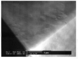
- FIG. 1 is an electron micrograph showing an example of a state in which a concave portion is formed in the texture structure. As shown in the enlarged photograph of FIG. 2, a concave portion is formed in the texture structure.
- the n + -type diffusion layer having a concave portion on the surface thereof is an n-type diffusion layer forming composition containing a glass powder containing n-type impurity atoms (hereinafter sometimes simply referred to as “glass powder”) and a dispersion medium. Is applied to a semiconductor substrate and fired. During firing, the glass component contained in the n-type diffusion layer forming composition that comes into contact with the semiconductor substrate locally reacts with the semiconductor substrate to form an amorphous portion. It is considered that a concave portion is formed on the surface of the n + -type diffusion layer by dissolving the amorphous portion with hydrofluoric acid or the like.
- the n-type diffusion layer forming composition in the present invention will be described first, and then a method for producing a solar cell substrate using the n-type diffusion layer forming composition will be described.
- the n-type diffusion layer forming composition contains glass powder containing n-type impurity atoms and a dispersion medium.
- the n-type diffusion layer forming composition may contain other additives as required in consideration of coating properties and the like.
- the n-type diffusion layer forming composition contains an n-type impurity atom and forms an n-type diffusion layer by thermally diffusing the n-type impurity into the semiconductor substrate after being applied to the semiconductor substrate. A material that can be used.
- the n-type impurity atoms by using the n-type diffusion layer forming composition comprising the glass powder, without forming an unnecessary n + -type diffusion layer on the back surface or the side surface, the n + -type diffusion layer at the desired site Can be formed.
- the n-type impurity atoms are bonded to the elements in the glass powder or are incorporated into the glass, so that the n-type impurities in the glass powder are not easily volatilized even during firing, and the surface is generated by the generation of volatilized gas. It is considered that the formation of the n-type diffusion layer on the back surface and side surfaces as well as on the surface is suppressed.
- the n-type impurity atom contained in the glass powder is an element capable of forming an n-type diffusion layer by diffusing into the semiconductor substrate.
- an element belonging to Group 15 can be used, and examples thereof include P (phosphorus), Sb (antimony), Bi (bismuth), As (arsenic), and the like.
- P or Sb is preferable from the viewpoints of safety, ease of vitrification, and the like.
- the n-type impurity atoms are preferably used in the state of an n-type impurity-containing substance that can be introduced into the glass powder.
- the n-type impurity-containing material used for introducing n-type impurity atoms into the glass powder include P 2 O 3 , P 2 O 5 , Sb 2 O 3 , and As 2 O 3 .
- the glass powder can control the melting temperature, softening temperature, glass transition temperature, chemical durability, and the like by adjusting the component ratio as necessary. Furthermore, it is preferable to contain the glass component substance described below.
- glass component materials include SiO 2 , K 2 O, Na 2 O, Li 2 O, BaO, SrO, CaO, MgO, BeO, ZnO, PbO, CdO, SnO, ZrO 2 , MoO 3 , La 2 O 3 , nb 2 O 5, Ta 2 O 5, Y 2 O 3, etc. TiO 2, ZrO 2, GeO 2 , TeO 2, Lu 2 O 3, V 2 O 5 and the like. Above all, at least selected from the group consisting of SiO 2 , K 2 O, Na 2 O, Li 2 O, BaO, SrO, CaO, MgO, BeO, ZnO, PbO, CdO, SnO, ZrO 2 , TiO 2 and MoO 3. One type is preferably used.
- the glass powder containing n-type impurity atoms include a system containing the n-type impurity-containing substance and the glass component substance.
- P 2 O 5 —SiO 2 system (described in the order of n-type impurity-containing substance-glass component substance, the same applies hereinafter), P 2 O 5 —K 2 O system, P 2 O 5 —Na 2 O system, P 2 O 5 -Li 2 O system, P 2 O 5 -BaO-based, P 2 O 5 -SrO based, P 2 O 5 -CaO-based, P 2 O 5 -MgO-based, P 2 O 5 -BeO , P 2 O 5 —ZnO, P 2 O 5 —CdO, P 2 O 5 —PbO, P 2 O 5 —V 2 O 5 , P 2 O 5 —SnO, P 2 O 5 — GeO 2 system, P 2 O 5 -TeO 2 system like system containing
- a glass powder containing two or more types of n-type impurity-containing substances such as P 2 O 5 —Sb 2 O 3 series, P 2 O 5 —As 2 O 3 series, or the like may be used.
- a glass powder containing two components is exemplified, but three or more components containing two or more kinds of glass component materials such as P 2 O 5 —SiO 2 —V 2 O 5 and P 2 O 5 —SiO 2 —CaO are included.
- the glass powder may be included.
- the content ratio of the glass component substance in the glass powder is preferably set as appropriate in consideration of the melting temperature, softening temperature, glass transition temperature, chemical durability, and the like.
- the content is preferably 0.1% by mass or more and 95% by mass or less, and more preferably 0.5% by mass or more and 90% by mass or less.
- the content ratio of CaO is preferably 1% by mass to 30% by mass, and preferably 5% by mass to 20% by mass. More preferably.
- the softening temperature of the glass powder is preferably 200 ° C. to 1000 ° C., more preferably 300 ° C. to 900 ° C., from the viewpoints of diffusibility during the diffusion treatment and dripping.
- the shape of the glass powder examples include a substantially spherical shape, a flat shape, a block shape, a plate shape, and a scale shape. From the viewpoint of application properties to the substrate and uniform diffusibility when an n-type diffusion layer forming composition is used, it is preferably substantially spherical, flat or plate-like.
- the particle size of the glass powder is desirably 100 ⁇ m or less. When glass powder having a particle size of 100 ⁇ m or less is used, a smooth coating film is easily obtained. Furthermore, the particle size of the glass powder is more preferably 50 ⁇ m or less, and further preferably 10 ⁇ m or less. The lower limit is not particularly limited, but is preferably 0.01 ⁇ m or more.
- the particle diameter of glass represents an average particle diameter, and can be measured by a laser scattering diffraction particle size distribution measuring apparatus or the like.
- the glass powder containing n-type impurity atoms is produced by the following procedure.
- raw materials for example, the n-type impurity-containing material and the glass component material are weighed and filled in a crucible.
- the material for the crucible include platinum, platinum-rhodium, iridium, alumina, quartz, carbon, and the like, which are appropriately selected in consideration of the melting temperature, atmosphere, reactivity with the molten material, and the like.
- the raw material is heated at a temperature corresponding to the glass composition in an electric furnace to obtain a melt. At this time, it is desirable to stir the melt uniformly.
- the obtained melt is poured onto a zirconia substrate, a carbon substrate or the like to vitrify the melt.
- the obtained glass is pulverized to form a powder.
- a known method such as a jet mill, a bead mill, or a ball mill can be applied to the pulverization.
- the content ratio of the glass powder containing n-type impurity atoms in the n-type diffusion layer forming composition is determined in consideration of coating properties, diffusibility of n-type impurity atoms, and the like. Generally, the content ratio of the glass powder in the n-type diffusion layer forming composition is preferably 0.1% by mass or more and 95% by mass or less, and more preferably 1% by mass or more and 90% by mass or less.
- the content ratio of the n-type impurity-containing substance containing n-type impurity atoms in the n-type diffusion layer forming composition is preferably 5% by mass or more and 30% by mass or less from the viewpoint of diffusion uniformity and glass layer removability. More preferably, it is 10 mass% or more and 20 mass% or less.
- the dispersion medium is a medium in which the glass powder is dispersed in the n-type diffusion layer forming composition.
- Specific examples of the dispersion medium include a binder, a solvent, a combination of a binder and a solvent, and the like.
- binder examples include polyvinyl alcohol, polyacrylamide resin, polyvinyl amide resin, polyvinyl pyrrolidone, polyethylene oxide resin, polysulfonic acid, acrylamide alkyl sulfonic acid, cellulose ether resin, cellulose derivative, carboxymethyl cellulose, hydroxyethyl cellulose, ethyl cellulose, gelatin, starch And starch derivatives, sodium alginate and sodium alginate derivatives, xanthan and xanthan derivatives, gua and gua derivatives, scleroglucan and scleroglucan derivatives, tragacanth and tragacanth derivatives, dextrin and dextrin derivatives, (meth) acrylic acid resin, (meth) Acrylic ester resin (eg, alkyl (meth) acrylate resin, dimethyl) Aminoethyl (meth) acrylate resin, etc.), butadiene resins, styrene resins
- the molecular weight of the binder is not particularly limited, and it is desirable to adjust appropriately in view of the desired viscosity as the composition. From the viewpoints of solubility in a solvent and handleability of the dissolved product, the weight average molecular weight of the binder is preferably 5,000 to 500,000, more preferably 10,000 to 200,000, still more preferably 20,000 to 100,000.
- the solvent examples include acetone, methyl ethyl ketone, methyl-n-propyl ketone, methyl-iso-propyl ketone, methyl-n-butyl ketone, methyl-iso-butyl ketone, methyl-n-pentyl ketone, methyl-n-hexyl ketone, Ketone solvents such as diethyl ketone, dipropyl ketone, di-iso-butyl ketone, trimethylnonanone, cyclohexanone, cyclopentanone, methylcyclohexanone, 2,4-pentanedione, acetonylacetone; diethyl ether, methyl ethyl ether, methyl- n-propyl ether, di-iso-propyl ether, tetrahydrofuran, methyltetrahydrofuran, dioxane, dimethyldio
- Acetonitrile N-methylpyrrolidinone, N-ethylpyrrolidinone, N-propylpyrrolidinone, N-butylpyrrolidinone, N-hexylpyrrolidinone, N-cyclohexylpyrrolidinone, N, N-dimethylformamide, N, N-dimethylacetamide, dimethylsulfoxide, etc.
- Aprotic polar solvent methanol, ethanol, n-propanol, i-propanol, n-butanol, i-butanol, sec-butanol, t-butanol, n-pentanol, i-pentanol, 2-methylbutanol, sec -Pentanol, t-pentanol, 3-methoxybutanol, n-hexanol, 2-methylpentanol, sec-hexanol, 2-ethylbutanol, sec-heptanol, n-octanol, 2-ethylhe Sanol, sec-octanol, n-nonyl alcohol, n-decanol, sec-undecyl alcohol, trimethylnonyl alcohol, sec-tetradecyl alcohol, sec-heptadecyl alcohol, phenol, cyclohexanol, methylcyclo
- the content ratio of the dispersion medium in the n-type diffusion layer forming composition is determined in consideration of the suitability for application to the semiconductor substrate and the n-type impurity concentration.
- the viscosity of the n-type diffusion layer forming composition is preferably 10 mPa ⁇ s or more and 1000000 mPa ⁇ s or less, more preferably 50 mPa ⁇ s or more and 500000 mPa ⁇ s or less in consideration of suitability for application to a semiconductor substrate. .
- a solar cell substrate manufacturing method in the case where a silicon substrate is used as a semiconductor substrate will be described as an example of a solar cell substrate manufacturing method.
- the damaged layer on the surface of the silicon substrate is removed by etching using an acidic or alkaline solution.
- a protective film made of a silicon oxide film or a silicon nitride film is formed on one surface of the silicon substrate.
- the silicon oxide film can be formed by, for example, an atmospheric pressure CVD method using silane gas and oxygen.
- the silicon nitride film can be formed by, for example, a plasma CVD method using silane gas, ammonia gas, and nitrogen gas.
- a fine uneven structure called a texture structure is formed on the surface of the silicon substrate where the protective film is not formed.
- the texture structure can be formed, for example, by immersing a silicon substrate on which a protective film is formed in a solution of about 80 ° C. containing potassium hydroxide and isopropyl alcohol (IPA). Subsequently, the protective film is etched away by immersing the silicon substrate in hydrofluoric acid.
- IPA isopropyl alcohol
- an n-type diffusion layer forming composition is applied on the p-type silicon substrate on the surface of the silicon substrate on which the texture structure is formed, along the shape of the light-receiving surface electrode.
- a shape which gives an n type diffused layer formation composition it can be set as a comb shape etc., for example.
- the width of the shape when the n-type diffusion layer forming composition is applied is preferably wider than the electrode width, and it is desirable to adjust appropriately according to the design of the electrode shape and the like. In general, it is preferable that the width is 5 ⁇ m to 100 ⁇ m wider than the electrode width.
- the method for applying the n-type diffusion layer forming composition is not particularly limited, and a commonly used method can be used. For example, it can be performed using a printing method such as a screen printing method or a gravure printing method, a spin method, a brush coating, a spray method, a doctor blade method, a roll coater method, an ink jet method or the like.
- a printing method such as a screen printing method or a gravure printing method, a spin method, a brush coating, a spray method, a doctor blade method, a roll coater method, an ink jet method or the like.
- the provision amount of the said n type diffused layer formation composition there is no restriction
- the amount of glass powder excluding the dispersion medium and the like can be 0.01 g / m 2 to 100 g / m 2 and 0.1 g / m 2. m 2 to 10 g / m 2 is preferable
- a heating step for removing at least a part of the dispersion medium may be provided.
- At least a part of the solvent can be volatilized by heat-treating the silicon substrate to which the n-type diffusion layer forming composition has been applied, for example, at 100 ° C. to 200 ° C. (specifically, for example, 150 ° C.).
- at least a part of the binder may be removed together with the solvent by heat treatment at 300 ° C. to 600 ° C. (specifically, for example, 450 ° C.).
- the silicon substrate to which the n-type diffusion layer forming composition is applied is heat-treated to form an n + -type diffusion layer having a high n-type impurity concentration.
- n-type impurities are diffused from the n-type diffusion layer forming composition into the silicon substrate to form an n + -type diffusion layer having a high n-type impurity concentration.
- the temperature of the heat treatment is preferably 800 ° C. to 1000 ° C., more preferably 850 ° C. to 950 ° C., and further preferably 870 ° C. to 900 ° C.
- the size of the n + type diffusion layer formed after the heat treatment should be 5 ⁇ m to 100 ⁇ m wider than the size (width) of the electrode in consideration of misalignment when the electrode is formed on the n + type diffusion layer. Is preferred.
- the width of the finger portion of the light-receiving surface electrode is 100 ⁇ m, it is preferable that the width of the n + -type diffusion layer under the finger portion is in the range of 105 ⁇ m to 200 ⁇ m.
- the n-type diffusion layer provides an n-type diffusion layer forming composition having a lower n-type impurity concentration than the n-type diffusion layer forming composition used in forming the n + -type diffusion layer, or an n-type impurity.
- the silicon substrate on which the n + type diffusion layer is formed is formed by heat treatment in an atmosphere including
- the n-type diffusion layer having a lower n-type impurity concentration than the n-type diffusion layer forming composition used when forming the n + -type diffusion layer A forming composition is used.
- an n + -type diffusion layer having a high n-type impurity concentration is formed in the electrode formation scheduled region, and n + -type diffusion layer is formed in the other region (light receiving region). It is possible to form an n-type diffusion layer having a low type impurity concentration.
- the method of forming the n-type diffusion layer by applying the n-type diffusion layer forming composition is not limited to the above method.
- an n + type diffusion layer forming composition having a high impurity concentration is applied to a silicon substrate in a pattern to form an n + type diffusion layer, and then an n type diffusion layer having a low n type impurity concentration is formed on the entire surface of the silicon substrate.
- An n-type diffusion layer may be formed by applying the composition.
- an n-type diffusion layer forming composition having a low impurity concentration is applied to the entire surface of the silicon substrate to form an n-type diffusion layer, and then an n-type diffusion layer forming composition having a high impurity concentration is applied in a pattern.
- An n + -type diffusion layer may be formed.
- the atmosphere containing the n-type impurity is not particularly limited as long as the atmosphere contains an n-type impurity.
- a mixed gas atmosphere of phosphorus oxychloride (POCl 3 ), nitrogen, and oxygen can be used.
- the heat treatment conditions are the same as the heat treatment conditions for forming the n + -type diffusion layer.
- the n + type diffusion layer forming composition (and the n type diffusion layer is formed by applying the n type diffusion layer forming composition). Since the glass layer derived from the glass component contained in the n-type diffusion layer forming composition) remains, the glass layer is preferably removed.
- the glass layer can be removed by a known method such as a method of immersing in an acid such as hydrofluoric acid or a method of immersing in an alkali such as caustic soda.
- the glass component contained in the n-type diffusion layer forming composition used when forming the n + -type diffusion layer locally reacts with the silicon substrate during firing to form an amorphous site. Is forming. It is considered that a concave portion is formed on the surface of the n + -type diffusion layer by dissolving the amorphous portion with an acid such as hydrofluoric acid. On the other hand, a recess such as an n + -type diffusion layer is not formed on the surface of the n-type diffusion layer, or the size of the recess is extremely small. For this reason, the surface roughness of the two is different, so that the region where the n + -type diffusion layer is formed and the region where the n-type diffusion layer is formed can be distinguished.
- the n-type diffusion layer forming composition When forming the n-type diffusion layer by applying the n-type diffusion layer forming composition, the n-type diffusion layer forming composition has a low n impurity concentration. Can be small. For this reason, the surface roughness of the light receiving region where the n-type diffusion layer is formed can be made substantially zero, and the power generation performance is not affected.
- the center line average roughness Ra of the surface of the n + -type diffusion layer is preferably in the range of 0.004 ⁇ m to 0.100 ⁇ m, and preferably in the range of 0.007 ⁇ m to 0.080 ⁇ m. More preferably, it is in the range of 0.010 ⁇ m to 0.050 ⁇ m.
- Ra is 0.100 ⁇ m or less, the disappearance of the diffusion region having a high n-type impurity concentration can be suppressed.
- it is 0.004 ⁇ m or more, it becomes easy to identify the n + -type diffusion layer.
- the center line average roughness Ra of the surface of the n + -type diffusion layer is a value measured according to the method of JIS B0601.
- the object to be measured is a part of an n + -type diffusion layer formed on the texture structure on the surface of the semiconductor substrate, and is a square pyramid having a height of about 5 ⁇ m and a base of about 20 ⁇ m. It is located on a small triangular surface that is one surface. For this reason, the evaluation length was 5 ⁇ m.
- the cut-off value ⁇ c for removing the swell component is not particularly necessary. The evaluation length may be longer than 5 ⁇ m. In this case, it is necessary to remove the unevenness of the texture structure on the surface of the n + -type diffusion layer by cutoff.
- VK-9700 shape measuring laser microscope
- NA 150 ⁇ objective lens
- Mitutoyo roughness standard piece No. It is desirable to calibrate the measured value using 178-605 or the like.
- the n + -type diffusion sheet resistance of the layer is preferably 20 ⁇ / ⁇ ⁇ 60 ⁇ / ⁇ , 30 ⁇ / More preferably, it is ⁇ ⁇ 40 ⁇ / ⁇ .
- the sheet resistance is an arithmetic average value obtained by measuring 25 points by the four-probe method. For example, it can be measured at 25 ° C. using a Loresta-EP MCP-T360 type low resistivity meter manufactured by Mitsubishi Chemical Corporation.
- one recess may exist on the surface of the n + -type diffusion layer to satisfy the range of the centerline average roughness Ra, or the centerline average roughness Ra satisfies the above range by a plurality of recesses. It may be. In addition, when there are a plurality of recesses, the plurality of recesses may be present independently or may be continuous.
- the junction depth of the n + -type diffusion layer is preferably in the range of 0.5 ⁇ m to 3.0 ⁇ m, and more preferably in the range of 0.5 ⁇ m to 2.0 ⁇ m.
- the junction depth of the n + -type diffusion layer can be measured by secondary ion analysis (SIMS analysis) using IMS-7F (CAMECA).
- the n + -type diffusion layer preferably has a region having an n-type impurity concentration of 10 20 atoms / cm 3 or more in at least a part of a range of 0.10 ⁇ m to 1.00 ⁇ m in depth from the substrate surface. More preferably, the depth is at least part of the range of 0.12 ⁇ m to 1.00 ⁇ m.
- the diffusion concentration of n-type impurities decreases from the substrate surface toward the inside. Therefore, if the relationship between the n-type impurity concentration and the depth is satisfied, even if there is erosion of the substrate surface layer due to the glass component in the electrode, a good ohmic contact with the electrode in a region where the n-type impurity concentration is sufficiently high Contact can be obtained.
- the n-type impurity concentration in the depth direction can be measured using secondary ion analysis (SIMS analysis) by IMS-7F (manufactured by CAMECA).
- SIMS analysis secondary ion analysis
- the n-type diffusion layer having an n-type impurity concentration lower than that of the n + -type diffusion layer preferably has a sheet resistance of about 80 ⁇ / ⁇ to 120 ⁇ / ⁇ , and is 90 ⁇ / ⁇ to 100 ⁇ / ⁇ . Is more preferable.
- the n-type diffusion layer has a region having an n-type impurity concentration of 10 18 atoms / cm 3 to 10 20 atoms / cm 3 on at least a part of the surface (a range from the substrate surface to a depth of 0.025 ⁇ m). Preferably, it has a region of 10 19 atoms / cm 3 to 5 ⁇ 10 19 atoms / cm 3 .
- the junction depth of the n-type diffusion layer is preferably in the range of 0.1 ⁇ m to 0.4 ⁇ m, and more preferably in the range of 0.15 ⁇ m to 0.3 ⁇ m. By setting it as such junction depth, the recombination of the carrier produced
- the junction depth of the n-type diffusion layer can be measured by secondary ion analysis (SIMS analysis) using IMS-7F (CAMECA).
- Positioning can be performed with high accuracy. Therefore, it can also be used as a semiconductor substrate other than the solar cell application.
- the solar cell element of the present invention has the above-described solar cell substrate and an electrode provided on the n + -type diffusion layer in the solar cell substrate. Below, an example of the manufacturing method of a solar cell element is demonstrated.
- the solar cell substrate is obtained by removing the n + type diffusion layer formed on the semiconductor substrate and the glass layer on the n type diffusion layer.
- the surface of the solar cell substrate on which the n + type diffusion layer and the n type diffusion layer are formed becomes the light receiving surface.
- An antireflection film may be formed on the light receiving surface.
- a nitride film such as Si 3 N 4 can be formed by a plasma CVD method.
- the light-receiving surface electrode is obtained by applying a surface electrode metal paste containing metal particles and glass particles to the electrode formation planned region on the n + -type diffusion layer so as to have a desired shape, and firing the resultant. By doing so, it can be formed.
- the surface of the n + -type diffusion layer due to the presence of the recess, n + -type diffusion layer can check the formed regions can easily perform the positioning of the electrodes easily .
- the electrode alignment may be performed, for example, by mounting a CCD camera control positioning system on a screen printer.
- the back electrode can be formed, for example, by applying a back electrode paste containing a metal such as aluminum, silver, or copper to the back surface of the solar cell substrate, drying it, and baking it. At this time, a silver paste for forming a silver electrode may be partially provided on the back surface for connection between elements in the module process.
- the solar cell of this invention has the said solar cell element and the wiring material arrange
- the solar cell may be configured by connecting a plurality of solar cell elements via a wiring material and further sealing with a sealing material.
- the wiring material and the sealing material are not particularly limited, and can be appropriately selected from those normally used in the art.
- the solar cell element means one having a semiconductor substrate on which a pn junction is formed and an electrode formed on the semiconductor substrate.
- the solar cell is a state in which a wiring material is provided on the electrode of the solar cell element, and a plurality of solar cell elements are connected through the wiring material as necessary, and is sealed with a sealing resin or the like Means things.
- Example 1 (Preparation of solar cell substrate) Glass powder (P 2 O 5 , SiO 2 , CaO as main components, 50%, 43%, 7% respectively), ethyl cellulose, terpineol 10 g, 4 g, 86 g are mixed to form n-type diffusion layer forming composition A was prepared.
- the n-type diffusion layer forming composition A is screen-printed on the surface (light-receiving surface) on which a texture structure of a p-type silicon substrate (manufactured by PVG Solutions, thickness: 180 ⁇ m) is formed, and a finger portion having a width of 150 ⁇ m and 1 It was applied to the shape of an electrode including a bus bar portion having a width of 5 mm and dried at 150 ° C. for 10 minutes. And it heat-processed for 3 minutes at 350 degreeC, and removed the solvent and the binder. Next, heat treatment was performed in the atmosphere at 900 ° C. for 10 minutes to diffuse n-type impurities into the silicon substrate. As a result, an n + -type diffusion layer was formed corresponding to the electrode formation scheduled region.
- n-type diffusion layer was formed in the light receiving region (region other than the electrode formation region) of the light receiving surface by diffusing in the silicon substrate. Subsequently, the glass layer remaining on the surface of the silicon substrate was removed with hydrofluoric acid. On the surface of the formed n + -type diffusion layer, a plurality of concave portions were continuously present on one surface.
- the center line average roughness Ra of the n + -type diffusion layer was 0.05 ⁇ m.
- the average value of the sheet resistance of the n + -type diffusion layer was 40 ⁇ / ⁇ , and the average value of the sheet resistance of the n-type diffusion layer was 102 ⁇ / ⁇ .
- a region having an n-type impurity concentration of 10 20 atoms / cm 3 or more was formed in a range from the substrate surface to a depth of 0.13 ⁇ m.
- a region having an n-type impurity concentration of 10 20 atoms / cm 3 was formed on the surface of the n-type diffusion layer.
- the junction depth of the n + -type diffusion layer was 0.5 ⁇ m, and the junction depth of the n-type diffusion layer was 0.2 ⁇ m.
- an antireflection film made of Si 3 N 4 is formed on the light-receiving surface of the silicon substrate on which the n + -type diffusion layer and the n-type diffusion layer are formed, a surface electrode is formed in the electrode formation region, and a back electrode is formed on the back surface.
- the finger part of the surface electrode was 100 ⁇ m wide, and the bus bar part was 1.1 mm wide.
- the surface electrode was formed by applying a silver electrode paste (manufactured by DuPont, trade name: Ag paste 159A) and the back electrode by applying an aluminum electrode paste (manufactured by PVG Solutions, trade name: Hyper BSF Al paste) with a screen printer. .
- the surface electrode on the light receiving surface and the n + -type diffusion layer were aligned by a CCD camera control positioning system.
- a positional shift (a surface electrode is formed in a region where the n + -type diffusion layer is not formed) is seen. There wasn't. Further, the region where the n + -type diffusion layer is formed is approximately 25 ⁇ m wider than both ends of the finger portion of the surface electrode (the region where the n + -type diffusion layer is formed protrudes from the both ends of the finger portion of the surface electrode by about 25 ⁇ m). Confirmed).
- the conversion efficiency of the solar cell element produced in the above process was measured and evaluated. Specifically, simulated sunlight (Wacom Denso Co., Ltd., trade name WXS-155S-10), current-voltage (IV) evaluation measuring instrument (IV CURVE TRACER MP-160, manufactured by EKO INSTRUMENT Co., Ltd.) ). Eff (conversion efficiency) indicating the power generation performance as a solar cell can be obtained by measuring in accordance with JIS-C-8912 and JIS-C-8913. The conversion efficiency of the obtained solar cell element was improved by 0.5% as compared with the solar cell element in which the n + -type diffusion layer was not formed (having no selective emitter structure).
- Example 2 A solar cell substrate was produced in the same manner as in Example 1 except that the heat treatment temperature for forming the n + -type diffusion layer was 950 ° C. for 10 minutes.
- the average value of the sheet resistance of the n + -type diffusion layer was 30 ⁇ / ⁇ , and the average value of the sheet resistance of the n-type diffusion layer was 102 ⁇ / ⁇ .
- On the surface of the n + -type diffusion layer a plurality of concave portions were continuously present on one surface.
- the surface roughness Ra of the n + -type diffusion layer was 0.08 ⁇ m.
- an n-type impurity concentration region of 10 20 atoms / cm 3 or more was formed in a range from the substrate surface to a depth of 0.20 ⁇ m.
- a region having an n-type impurity concentration of 10 20 atoms / cm 3 was formed on the surface of the n-type diffusion layer.
- the junction depth of the n + -type diffusion layer was 0.7 ⁇ m, and the junction depth of the n-type diffusion layer was 0.2 ⁇ m.
- a solar cell element was produced in the same manner as in Example 1.
- the formation position of the surface electrode and the region of the n + -type diffusion layer were observed with a microscope and compared with each other, no displacement was observed.
- the region where the n + -type diffusion layer was formed was wider by 25 ⁇ m on both ends with respect to the electrode.
- the conversion efficiency of the obtained solar cell element was improved by 0.6% compared to a solar cell element in which an n + -type diffusion layer was not formed (having no selective emitter structure).
- Example 1 A solar cell substrate was produced in the same manner as in Example 1 except that the n + -type diffusion layer was formed by using a diffusion solution containing ammonium phosphate and performing heat treatment at 900 ° C. for 10 minutes.
- the average value of the sheet resistance of the n + -type diffusion layer was 40 ⁇ / ⁇ , and the average value of the sheet resistance of the n-type diffusion layer was 102 ⁇ / ⁇ . No recess was found on the surface of the n + type diffusion layer. As a result, it was difficult to distinguish the region where the n + -type diffusion layer was formed from the region where the n-type diffusion layer was formed.
- a solar cell element was produced in the same manner as in Example 1.
- the location where the position of the electrode formed on the light-receiving surface did not coincide with the n + -type diffusion layer was confirmed.
- the conversion efficiency of the obtained solar cell element was not improved as compared with the solar cell element in which the n + -type diffusion layer was not formed (having no selective emitter structure). It was also confirmed that the fill factor due to contact resistance was significantly reduced. This is presumably because the position where the n + -type diffusion layer is formed and the position of the electrode formed thereon are displaced, and the electrode is in contact with the n-type diffusion layer.
Landscapes
- Photovoltaic Devices (AREA)
Abstract
Description
しかしながら、その形成された拡散層上に受光面の電極を形成する工程で、周囲の領域と比較して、不純物濃度の高い領域の識別が困難となっており、電極が不純物濃度の高い拡散領域の上からずれて形成されることがある。そのため、不純物濃度の低い受光領域と電極とが接触することで接触抵抗が高くなることがあった。そこで一般に電極ペースト印刷時には、ウエハに印を施して、CCDカメラ制御位置づけシステムにより、不純物濃度の高い拡散領域と電極の位置づけを実施している。しかしながら、このような方法を採用しても100μm程度の幅のフィンガー電極は僅かなアライメントの差で、大きく位置ずれを起こすことがある。
<1>n型拡散層と、前記n型拡散層よりもn型不純物濃度の高いn+型拡散層と、を有し、前記n+型拡散層の表面に凹部を有する半導体基板である太陽電池基板。
前記n型拡散層形成組成物が付与された半導体基板に熱拡散処理を施す工程と、
を有する<1>~<8>のいずれか1項に記載の太陽電池基板の製造方法。
前記太陽電池基板におけるn+型拡散層上に設けられた電極と、
を有する太陽電池素子。
本発明の太陽電池基板は、n型拡散層と、前記n型拡散層よりもn型不純物濃度の高いn+型拡散層と、を有し、前記n+型拡散層の表面が凹部を有する半導体基板である。
一方、前記n+型拡散層よりもn型不純物濃度の低いn型拡散層は、受光面電極が形成されずに受光面となる位置に形成される。n型拡散層のn型不純物濃度がn+型拡散層よりも低いことで、短波長側の光を有効に利用でき、また生成キャリアの再結合損失を抑制することができる。
前記n型拡散層形成組成物は、n型不純物原子を含むガラス粉末と、分散媒とを含有する。前記n型拡散層形成組成物は、塗布性などを考慮してその他の添加剤を必要に応じて含有してもよい。
ここで、n型拡散層形成組成物とは、n型不純物原子を含有し、半導体基板に付与した後に前記n型不純物を前記半導体基板中に熱拡散することでn型拡散層を形成することが可能な材料をいう。
前記ガラス粉末は、必要に応じて成分比率を調整することによって、溶融温度、軟化温度、ガラス転移温度、化学的耐久性等を制御することが可能である。更に以下に記すガラス成分物質を含むことが好ましい。
具体的には、P2O5-SiO2系(n型不純物含有物質-ガラス成分物質の順で記載、以下同様)、P2O5-K2O系、P2O5-Na2O系、P2O5-Li2O系、P2O5-BaO系、P2O5-SrO系、P2O5-CaO系、P2O5-MgO系、P2O5-BeO系、P2O5-ZnO系、P2O5-CdO系、P2O5-PbO系、P2O5-V2O5系、P2O5-SnO系、P2O5-GeO2系、P2O5-TeO2系等のn型不純物含有物質としてP2O5を含む系、前記のP2O5を含む系のP2O5の代わりにn型不純物含有物質としてSb2O3を含む系のガラス粉末などが挙げられる。
なお、P2O5-Sb2O3系、P2O5-As2O3系等のように、2種類以上のn型不純物含有物質を含むガラス粉末でもよい。
上記では2成分を含むガラス粉末を例示したが、P2O5-SiO2-V2O5、P2O5-SiO2-CaOなどの2種類以上のガラス成分物質を含む3成分以上を含むガラス粉末でもよい。
具体的には、P2O5-SiO2-CaO系ガラスの場合には、CaOの含有比率は、1質量%以上30質量%以下であることが好ましく、5質量%以上20質量%以下であることがより好ましい。
またガラス粉末の粒径は、100μm以下であることが望ましい。100μm以下の粒径を有するガラス粉末を用いた場合には、平滑な塗膜が得られやすい。更に、ガラス粉末の粒径は50μm以下であることがより望ましく、10μm以下がさらに望ましい。なお、下限は特に制限されないが、0.01μm以上であることが好ましい。
ここで、ガラスの粒径は、平均粒子径を表し、レーザー散乱回折法粒度分布測定装置等により測定することができる。
最初に原料、例えば、前記n型不純物含有物質とガラス成分物質を秤量し、るつぼに充填する。るつぼの材質としては白金、白金-ロジウム、イリジウム、アルミナ、石英、炭素などが挙げられるが、溶融温度、雰囲気、溶融物質との反応性等を考慮して適宜選ばれる。
次に、前記原料を電気炉でガラス組成に応じた温度で加熱し融液とする。このとき融液が均一となるよう攪拌することが望ましい。
続いて得られた融液をジルコニア基板やカーボン基板等の上に流し出して融液をガラス化する。
最後に得られたガラスを粉砕し粉末状とする。粉砕にはジェットミル、ビーズミル、ボールミル等公知の方法が適用できる。
n型拡散層形成組成物中のn型不純物原子を含むn型不純物含有物質の含有比率は、拡散均一性およびガラス層の除去性の観点から5質量%以上30質量%以下であることが好ましく、10質量%以上20質量%以下であることがより好ましい。
分散媒とは、n型拡散層形成組成物中において上記ガラス粉末を分散させる媒体である。具体的な分散媒の例としては、バインダーや溶剤、バインダーと溶剤の組み合わせ等が挙げられる。
バインダーとしては、例えば、ポリビニルアルコール、ポリアクリルアミド樹脂、ポリビニルアミド樹脂、ポリビニルピロリドン、ポリエチレンオキサイド樹脂、ポリスルホン酸、アクリルアミドアルキルスルホン酸、セルロースエーテル樹脂、セルロース誘導体、カルボキシメチルセルロース、ヒドロキシエチルセルロース、エチルセルロース、ゼラチン、澱粉及び澱粉誘導体、アルギン酸ナトリウム及びアルギン酸ナトリウム誘導体、キサンタン及びキサンタン誘導体、グア及びグア誘導体、スクレログルカン及びスクレログルカン誘導体、トラガカント及びトラガカント誘導体、デキストリン及びデキストリン誘導体、(メタ)アクリル酸樹脂、(メタ)アクリル酸エステル樹脂(例えば、アルキル(メタ)アクリレート樹脂、ジメチルアミノエチル(メタ)アクリレート樹脂等)、ブタジエン樹脂、スチレン樹脂、又はこれらの共重合体などが挙げられる。他にも、シロキサン樹脂を適宜選択しうる。これらのバインダーは1種類を単独で又は2種類以上を組み合わせて使用される。
溶剤としては、例えば、アセトン、メチルエチルケトン、メチル-n-プロピルケトン、メチル-iso-プロピルケトン、メチル-n-ブチルケトン、メチル-iso-ブチルケトン、メチル-n-ペンチルケトン、メチル-n-ヘキシルケトン、ジエチルケトン、ジプロピルケトン、ジ-iso-ブチルケトン、トリメチルノナノン、シクロヘキサノン、シクロペンタノン、メチルシクロヘキサノン、2,4-ペンタンジオン、アセトニルアセトン等のケトン溶剤;ジエチルエーテル、メチルエチルエーテル、メチル-n-プロピルエーテル、ジ-iso-プロピルエーテル、テトラヒドロフラン、メチルテトラヒドロフラン、ジオキサン、ジメチルジオキサン、エチレングリコールジメチルエーテル、エチレングリコールジエチルエーテル、エチレングリコールジ-n-プロピルエーテル、エチレングリコールジブチルエーテル、ジエチレングリコールジメチルエーテル、ジエチレングリコールジエチルエーテル、ジエチレングリコールメチルエチルエーテル、ジエチレングリコールメチル-n-プロピルエーテル、ジエチレングリコールメチル-n-ブチルエーテル、ジエチレングリコールジ-n-プロピルエーテル、ジエチレングリコールジ-n-ブチルエーテル、ジエチレングリコールメチル-n-ヘキシルエーテル、トリエチレングリコールジメチルエーテル、トリエチレングリコールジエチルエーテル、トリエチレングリコールメチルエチルエーテル、トリエチレングリコールメチル-n-ブチルエーテル、トリエチレングリコールジ-n-ブチルエーテル、トリエチレングリコールメチル-n-ヘキシルエーテル、テトラエチレングリコールジメチルエーテル、テトラエチレングリコールジエチルエーテル、テトラジエチレングリコールメチルエチルエーテル、テトラエチレングリコールメチル-n-ブチルエーテル、ジエチレングリコールジ-n-ブチルエーテル、テトラエチレングリコールメチル-n-ヘキシルエーテル、テトラエチレングリコールジ-n-ブチルエーテル、プロピレングリコールジメチルエーテル、プロピレングリコールジエチルエーテル、プロピレングリコールジ-n-プロピルエーテル、プロピレングリコールジブチルエーテル、ジプロピレングリコールジメチルエーテル、ジプロピレングリコールジエチルエーテル、ジプロピレングリコールメチルエチルエーテル、ジプロピレングリコールメチル-n-ブチルエーテル、ジプロピレングリコールジ-n-プロピルエーテル、ジプロピレングリコールジ-n-ブチルエーテル、ジプロピレングリコールメチル-n-ヘキシルエーテル、トリプロピレングリコールジメチルエーテル、トリプロピレングリコールジエチルエーテル、トリプロピレングリコールメチルエチルエーテル、トリプロピレングリコールメチル-n-ブチルエーテル、トリプロピレングリコールジ-n-ブチルエーテル、トリプロピレングリコールメチル-n-ヘキシルエーテル、テトラプロピレングリコールジメチルエーテル、テトラプロピレングリコールジエチルエーテル、テトラジプロピレングリコールメチルエチルエーテル、テトラプロピレングリコールメチル-n-ブチルエーテル、ジプロピレングリコールジ-n-ブチルエーテル、テトラプロピレングリコールメチル-n-ヘキシルエーテル、テトラプロピレングリコールジ-n-ブチルエーテル等のエーテル溶剤;
上記で得られたn型不純物原子を含むガラス粉末と、分散媒とを混合することでn型拡散層形成組成物が得られる。
n型拡散層形成組成物の粘度は、半導体基板への付与適性を考慮して、10mPa・s以上1000000mPa・s以下であることが好ましく、50mPa・s以上500000mPa・s以下であることがより好ましい。
以下、太陽電池基板の製造方法の一例として半導体基板としてシリコン基板を用いた場合の太陽電池基板の製造方法について説明する。
まず、シリコン基板の表面にあるダメージ層を、酸性あるいはアルカリ性の溶液を用いてエッチングして除去する。
次に、シリコン基板の一方の表面に珪素の酸化物膜あるいは珪素の窒化物膜からなる保護膜を形成する。ここで、珪素の酸化物膜は、たとえばシランガスと酸素を用いた常圧CVD法により形成することができる。また、珪素の窒化物膜は、たとえば、シランガス、アンモニアガス及び窒素ガスを用いたプラズマCVD法により形成することができる。
続いて、シリコン基板をフッ酸に浸漬させることによって、保護膜をエッチング除去する。
前記n型拡散層形成組成物の付与量としては特に制限はない。例えば、n型拡散層形成組成物がガラスペーストの状態である場合は、分散媒等を除いたガラス粉末量として0.01g/m2~100g/m2とすることができ、0.1g/m2~10g/m2であることが好ましい。
前記熱処理の温度は800℃~1000℃であることが好ましく、さらに850℃以上950℃以下がより好ましく、870℃以上900℃以下がさらに好ましい。
前記太陽電池基板のn+型拡散層の表面には凹部が存在する。この凹部の存在によって前記n+型拡散層の表面の中心線平均粗さRaは、0.004μm~0.100μmの範囲であることが好ましく、0.007μm~0.080μmの範囲であることがより好ましく、0.010μm~0.050μmの範囲であることが更に好ましい。Raが0.100μm以下の場合には、n型不純物濃度の高い拡散領域の消失が抑えられる。また、0.004μm以上の場合には、n+型拡散層を識別しやすくなる。
なお、シート抵抗は、四探針法により25点測定した結果の算術平均値である。例えば、三菱化学(株)製Loresta-EP MCP-T360型低抵抗率計を用いて25℃で測定することができる。
本発明の太陽電池素子は、上述の太陽電池基板と、前記太陽電池基板におけるn+型拡散層上に設けられた電極と、を有する。以下では、太陽電池素子の製造方法の一例を説明する。
前記受光面上には、反射防止膜を形成してもよい。反射防止膜としては、例えばSi3N4などの窒化物膜をプラズマCVD法により形成することができる。
例えば、受光面電極(表面電極)は、金属粒子及びガラス粒子を含む表面電極用金属ペーストを、n+型拡散層上の電極形成予定領域に所望の形状となるよう付与し、これを焼成処理することで形成することができる。
本発明の太陽電池は、前記太陽電池素子と、太陽電池素子の電極上に配置された配線材料と、を有する。前記太陽電池はさらに必要に応じて、配線材料を介して複数の太陽電池素子が連結され、さらに封止材で封止されて構成されていてもよい。
前記配線材料及び封止材の材料は特に制限されず、当業界で通常用いられているものから適宜選択することができる。
尚、本明細書において太陽電池素子とは、pn接合が形成された半導体基板と、半導体基板上に形成された電極とを有するものを意味する。また太陽電池とは、太陽電池素子の電極上に配線材料が設けられ、必要に応じて複数の太陽電池素子が配線材料を介して接続されて構成され、封止樹脂等で封止された状態のものを意味する。
(太陽電池基板の作製)
ガラス粉末(P2O5、SiO2、CaOを主成分とし、それぞれ50%、43%、7%)、エチルセルロース、テルピネオールをそれぞれ10g、4g、86g混合して、n型拡散層形成組成物Aを調製した。
前記n+型拡散層中で、1020atoms/cm3以上のn型不純物濃度の領域が、基板表面から深さ0.13μmまでの範囲に形成されていた。
前記n型拡散層の表面には1020atoms/cm3のn型不純物濃度の領域が形成されていた。
前記n+型拡散層の接合深さは0.5μmであり、前記n型拡散層の接合深さは、0.2μmであった。
常法により、前記n+型拡散層及び前記n型拡散層が形成されたシリコン基板の受光面にSi3N4からなる反射防止膜を、電極形成領域に表面電極を、裏面に裏面電極をそれぞれ形成して、太陽電池素子を作製した。なお、表面電極のフィンガー部は100μm幅、バスバー部は1.1mm幅であった。表面電極は銀電極ペースト(デュポン社製、商品名:Agペースト159A)、裏面電極はアルミ電極ペースト(PVG Solutions社製、商品名:Hyper BSF Alペースト)をそれぞれスクリーン印刷機で付与して形成した。
上記工程で作製した太陽電池素子の変換効率を測定し、評価を行った。
具体的には、擬似太陽光(株式会社ワコム電創製、商品名WXS-155S-10)と、電流―電圧(I-V)評価測定器(I-V CURVE TRACER MP-160、EKO INSTRUMENT社製)とを組み合わせて行った。太陽電池としての発電性能を示すEff(変換効率)は、JIS-C-8912、及びJIS-C-8913に準拠して測定を行うことで得られる。
得られた太陽電池素子は、n+型拡散層が形成されていない(選択エミッタ構造を有しない)太陽電池素子に比べて、変換効率が0.5%向上していた。
n+型拡散層を形成する際の熱処理温度を950℃で10分間とした以外は実施例1と同様にして太陽電池基板を作製した。n+型拡散層のシート抵抗の平均値は30Ω/□、n型拡散層のシート抵抗の平均値は102Ω/□であった。
n+型拡散層の表面には、複数の凹部が連なって一面に存在していた。n+型拡散層の表面粗さRaは0.08μmであった。
n+型拡散層の接合深さは0.7μmであり、n型拡散層の接合深さは、0.2μmであった。
得られた太陽電池素子は、n+型拡散層が形成されていない(選択エミッタ構造を有しない)太陽電池素子に比べて、変換効率が0.6%向上していた。
n+型拡散層をリン酸アンモニウムを含む拡散液を用いて、熱処理を900℃で10分間行って形成した以外は実施例1と同様にして太陽電池基板を作製した。n+型拡散層のシート抵抗の平均値は40Ω/□、n型拡散層のシート抵抗の平均値は102Ω/□であった。n+型拡散層の表面に凹部は見られなかった。その結果、n+型拡散層が形成された領域とn型拡散層が形成された領域とを識別するのが困難であった。
得られた太陽電池素子は、n+型拡散層が形成されていない(選択エミッタ構造を有しない)太陽電池素子に比べて、変換効率は向上していなかった。また、接触抵抗が起因する曲線因子(フィルファクター)が著しく低下していることを確認した。これはn+型拡散層が形成された領域とその上に形成された電極の位置にずれが生じており、電極がn型拡散層と接触しているためと考えられる。
Claims (11)
- n型拡散層と、前記n型拡散層よりもn型不純物濃度の高いn+型拡散層と、を有し、前記n+型拡散層の表面に凹部を有する半導体基板である太陽電池基板。
- 前記n+型拡散層の表面の中心線平均粗さRaが0.004μm~0.100μmである請求項1に太陽電池基板。
- 前記n+型拡散層はn型不純物濃度が1020atoms/cm3以上である領域を、表面から深さ0.10μm~1.00μmの範囲の少なくとも一部に有する請求項1又は請求項2に記載の太陽電池基板。
- 前記n+型拡散層のシート抵抗が、20Ω/□~60Ω/□である請求項1~請求項3のいずれか1項に記載の太陽電池基板。
- 前記n型拡散層は、表面に1018atoms/cm3~1020atoms/cm3のn型不純物濃度の領域を有し、且つ接合深さが0.1μm~0.4μmの範囲である請求項1~請求項4のいずれか1項に記載の太陽電池基板。
- 前記n+型拡散層が、n型不純物原子を含むガラス粉末と、分散媒と、を含有するn型拡散層形成組成物を塗布し、焼成して得られる請求項1~請求項5のいずれか1項に記載の太陽電池基板。
- 前記n型不純物原子が、P(リン)及びSb(アンチモン)からなる群より選択される少なくとも1種である請求項6に記載の太陽電池基板。
- 前記n型不純物原子を含むガラス粉末が、P2O3、P2O5及びSb2O3からなる群より選択される少なくとも1種のn型不純物含有物質と、SiO2、K2O、Na2O、Li2O、BaO、SrO、CaO、MgO、BeO、ZnO、PbO、CdO、SnO、ZrO2、TiO2及びMoO3からなる群より選択される少なくとも1種のガラス成分物質と、を含有する請求項6又は請求項7に記載の太陽電池基板。
- 半導体基板上に、n型不純物原子を含むガラス粉末と、分散媒と、を含有するn型拡散層形成組成物を付与する工程と、
前記n型拡散層形成組成物が付与された半導体基板に熱拡散処理を施す工程と、
を有する請求項1~請求項8のいずれか1項に記載の太陽電池基板の製造方法。 - 請求項1~請求項8のいずれか1項に記載の太陽電池基板と、
前記太陽電池基板におけるn+型拡散層上に設けられた電極と、
を有する太陽電池素子。 - 請求項10に記載の太陽電池素子と、前記太陽電池素子の電極上に配置された配線材料と、を有する太陽電池。
Priority Applications (2)
| Application Number | Priority Date | Filing Date | Title |
|---|---|---|---|
| CN201280035335.6A CN103688367A (zh) | 2011-07-25 | 2012-07-18 | 太阳能电池基板、太阳能电池基板的制造方法、太阳能电池元件及太阳能电池 |
| KR1020147001164A KR101541657B1 (ko) | 2011-07-25 | 2012-07-18 | 태양 전지 기판, 태양 전지 기판의 제조 방법, 태양 전지 소자 및 태양 전지 |
Applications Claiming Priority (2)
| Application Number | Priority Date | Filing Date | Title |
|---|---|---|---|
| JP2011162610 | 2011-07-25 | ||
| JP2011-162610 | 2011-07-25 |
Publications (1)
| Publication Number | Publication Date |
|---|---|
| WO2013015173A1 true WO2013015173A1 (ja) | 2013-01-31 |
Family
ID=47596221
Family Applications (1)
| Application Number | Title | Priority Date | Filing Date |
|---|---|---|---|
| PCT/JP2012/068234 Ceased WO2013015173A1 (ja) | 2011-07-25 | 2012-07-18 | 太陽電池基板、太陽電池基板の製造方法、太陽電池素子及び太陽電池 |
Country Status (6)
| Country | Link |
|---|---|
| US (1) | US20130025669A1 (ja) |
| JP (3) | JPWO2013015173A1 (ja) |
| KR (1) | KR101541657B1 (ja) |
| CN (1) | CN103688367A (ja) |
| TW (1) | TWI607575B (ja) |
| WO (1) | WO2013015173A1 (ja) |
Families Citing this family (7)
| Publication number | Priority date | Publication date | Assignee | Title |
|---|---|---|---|---|
| JP2013211541A (ja) * | 2012-02-28 | 2013-10-10 | Kyocera Corp | 太陽電池素子および太陽電池素子の製造方法 |
| JP6523885B2 (ja) * | 2015-09-11 | 2019-06-05 | 株式会社東芝 | 半導体装置 |
| CN110100317B (zh) * | 2016-12-13 | 2022-09-30 | 信越化学工业株式会社 | 高效背面接触型太阳能电池单元、太阳能电池组件和光伏发电系统 |
| CN118053922A (zh) | 2023-12-15 | 2024-05-17 | 浙江晶科能源有限公司 | 太阳能电池及其制备方法、光伏组件 |
| CN119008726A (zh) | 2023-12-15 | 2024-11-22 | 浙江晶科能源有限公司 | 太阳能电池及其制备方法、光伏组件 |
| CN118053927A (zh) | 2023-12-15 | 2024-05-17 | 浙江晶科能源有限公司 | 太阳能电池及其制备方法、光伏组件 |
| CN118053928A (zh) | 2023-12-15 | 2024-05-17 | 浙江晶科能源有限公司 | 太阳能电池及光伏组件 |
Citations (6)
| Publication number | Priority date | Publication date | Assignee | Title |
|---|---|---|---|---|
| JPH04122012A (ja) * | 1990-09-12 | 1992-04-22 | Mitsubishi Electric Corp | アライメントマークおよびその形成方法 |
| JP2006310373A (ja) * | 2005-04-26 | 2006-11-09 | Shin Etsu Handotai Co Ltd | 太陽電池の製造方法及び太陽電池並びに半導体装置の製造方法 |
| JP2008053363A (ja) * | 2006-08-23 | 2008-03-06 | Matsushita Electric Ind Co Ltd | 半導体基板およびその製造方法 |
| JP2008282912A (ja) * | 2007-05-09 | 2008-11-20 | Mitsubishi Electric Corp | 太陽電池素子の製造方法 |
| WO2010068331A1 (en) * | 2008-12-10 | 2010-06-17 | Applied Materials, Inc. | Enhanced vision system for screen printing pattern alignment |
| JP2011023690A (ja) * | 2009-07-20 | 2011-02-03 | E-Ton Solar Tech Co Ltd | 選択エミッタ構造の電極パターンのアラインメント方法 |
Family Cites Families (16)
| Publication number | Priority date | Publication date | Assignee | Title |
|---|---|---|---|---|
| US4137123A (en) * | 1975-12-31 | 1979-01-30 | Motorola, Inc. | Texture etching of silicon: method |
| DE69708463T2 (de) * | 1996-02-27 | 2002-05-16 | Canon K.K., Tokio/Tokyo | Photovoltaische Vorrichtung, die ein undurchsichtiges Substrat mit einer spezifischen unregelmässigen Oberflächenstruktur aufweist |
| JP3719047B2 (ja) * | 1999-06-07 | 2005-11-24 | 日亜化学工業株式会社 | 窒化物半導体素子 |
| JP2004273829A (ja) * | 2003-03-10 | 2004-09-30 | Sharp Corp | 光電変換装置及びその製造方法 |
| TW200504384A (en) * | 2003-07-24 | 2005-02-01 | Zeon Corp | Molded article for anti-reflection and method for preparing the article |
| JP2007294295A (ja) * | 2006-04-26 | 2007-11-08 | Nippon Zeon Co Ltd | 直下型バックライト装置 |
| US8975172B2 (en) * | 2006-09-27 | 2015-03-10 | Kyocera Corporation | Solar cell element and method for manufacturing solar cell element |
| NL2000999C2 (nl) * | 2007-11-13 | 2009-05-14 | Stichting Energie | Werkwijze voor het fabriceren van kristallijn silicium zonnecellen met gebruikmaking van co-diffusie van boor en fosfor. |
| JP5438986B2 (ja) * | 2008-02-19 | 2014-03-12 | 株式会社半導体エネルギー研究所 | 光電変換装置の製造方法 |
| TW200941750A (en) * | 2008-03-21 | 2009-10-01 | Contrel Technology Co Ltd | Improved terrace structure for solar cell |
| WO2009145857A1 (en) * | 2008-04-18 | 2009-12-03 | 1366 Technologies Inc. | Methods to pattern diffusion layers in solar cells and solar cells made by such methods |
| JP5815215B2 (ja) * | 2009-08-27 | 2015-11-17 | 東京応化工業株式会社 | 拡散剤組成物、および不純物拡散層の形成方法 |
| JP5537101B2 (ja) * | 2009-09-10 | 2014-07-02 | 株式会社カネカ | 結晶シリコン系太陽電池 |
| TWI449198B (zh) * | 2009-10-05 | 2014-08-11 | Nat Univ Tsing Hua | Selective emitter solar cell process |
| US20110126877A1 (en) * | 2009-11-27 | 2011-06-02 | Jinah Kim | Solar cell |
| US8187979B2 (en) * | 2009-12-23 | 2012-05-29 | Varian Semiconductor Equipment Associates, Inc. | Workpiece patterning with plasma sheath modulation |
-
2012
- 2012-07-18 JP JP2013525683A patent/JPWO2013015173A1/ja active Pending
- 2012-07-18 WO PCT/JP2012/068234 patent/WO2013015173A1/ja not_active Ceased
- 2012-07-18 CN CN201280035335.6A patent/CN103688367A/zh active Pending
- 2012-07-18 KR KR1020147001164A patent/KR101541657B1/ko not_active Expired - Fee Related
- 2012-07-24 US US13/556,850 patent/US20130025669A1/en not_active Abandoned
- 2012-07-25 TW TW101126717A patent/TWI607575B/zh not_active IP Right Cessation
-
2015
- 2015-04-14 JP JP2015082316A patent/JP2015149500A/ja active Pending
-
2016
- 2016-05-10 JP JP2016094541A patent/JP2016139834A/ja active Pending
Patent Citations (6)
| Publication number | Priority date | Publication date | Assignee | Title |
|---|---|---|---|---|
| JPH04122012A (ja) * | 1990-09-12 | 1992-04-22 | Mitsubishi Electric Corp | アライメントマークおよびその形成方法 |
| JP2006310373A (ja) * | 2005-04-26 | 2006-11-09 | Shin Etsu Handotai Co Ltd | 太陽電池の製造方法及び太陽電池並びに半導体装置の製造方法 |
| JP2008053363A (ja) * | 2006-08-23 | 2008-03-06 | Matsushita Electric Ind Co Ltd | 半導体基板およびその製造方法 |
| JP2008282912A (ja) * | 2007-05-09 | 2008-11-20 | Mitsubishi Electric Corp | 太陽電池素子の製造方法 |
| WO2010068331A1 (en) * | 2008-12-10 | 2010-06-17 | Applied Materials, Inc. | Enhanced vision system for screen printing pattern alignment |
| JP2011023690A (ja) * | 2009-07-20 | 2011-02-03 | E-Ton Solar Tech Co Ltd | 選択エミッタ構造の電極パターンのアラインメント方法 |
Also Published As
| Publication number | Publication date |
|---|---|
| TW201310677A (zh) | 2013-03-01 |
| JPWO2013015173A1 (ja) | 2015-02-23 |
| TWI607575B (zh) | 2017-12-01 |
| KR20140027471A (ko) | 2014-03-06 |
| JP2015149500A (ja) | 2015-08-20 |
| US20130025669A1 (en) | 2013-01-31 |
| JP2016139834A (ja) | 2016-08-04 |
| KR101541657B1 (ko) | 2015-08-03 |
| CN103688367A (zh) | 2014-03-26 |
Similar Documents
| Publication | Publication Date | Title |
|---|---|---|
| JP2016139834A (ja) | 太陽電池基板、太陽電池基板の製造方法、太陽電池素子及び太陽電池 | |
| WO2011090216A1 (ja) | n型拡散層形成組成物、n型拡散層の製造方法、及び太陽電池セルの製造方法 | |
| KR20140041797A (ko) | 반도체 기판 및 그 제조 방법, 태양 전지 소자, 그리고 태양 전지 | |
| WO2012067119A1 (ja) | 太陽電池の製造方法 | |
| JP5935254B2 (ja) | 不純物拡散層形成組成物、不純物拡散層の製造方法、太陽電池素子の製造方法および太陽電池の製造方法 | |
| JP5867256B2 (ja) | 太陽電池の製造方法 | |
| JP6203496B2 (ja) | 太陽電池の製造方法 | |
| JP2013026344A (ja) | n型拡散層の製造方法、太陽電池素子の製造方法、および太陽電池素子 | |
| JP2013026343A (ja) | p型拡散層の製造方法、太陽電池素子の製造方法、および太陽電池素子 | |
| US20120122264A1 (en) | Method for producing photovoltaic cell | |
| US20120122265A1 (en) | Method for producing photovoltaic cell | |
| US8404599B2 (en) | Method for producing photovoltaic cell | |
| JP5673694B2 (ja) | n型拡散層形成組成物、n型拡散層の製造方法、及び太陽電池セルの製造方法 | |
| JP2013026472A (ja) | n型拡散層形成組成物、n型拡散層の製造方法、及び太陽電池素子の製造方法 | |
| JP2013026477A (ja) | n型拡散層形成組成物、n型拡散層の製造方法、及び太陽電池素子の製造方法 | |
| JPWO2016068315A1 (ja) | n型拡散層形成組成物、n型拡散層の製造方法及び太陽電池素子の製造方法 |
Legal Events
| Date | Code | Title | Description |
|---|---|---|---|
| 121 | Ep: the epo has been informed by wipo that ep was designated in this application |
Ref document number: 12818185 Country of ref document: EP Kind code of ref document: A1 |
|
| ENP | Entry into the national phase |
Ref document number: 2013525683 Country of ref document: JP Kind code of ref document: A |
|
| ENP | Entry into the national phase |
Ref document number: 20147001164 Country of ref document: KR Kind code of ref document: A |
|
| NENP | Non-entry into the national phase |
Ref country code: DE |
|
| 122 | Ep: pct application non-entry in european phase |
Ref document number: 12818185 Country of ref document: EP Kind code of ref document: A1 |