WO2012176747A1 - 機能素子の製造方法 - Google Patents
機能素子の製造方法 Download PDFInfo
- Publication number
- WO2012176747A1 WO2012176747A1 PCT/JP2012/065562 JP2012065562W WO2012176747A1 WO 2012176747 A1 WO2012176747 A1 WO 2012176747A1 JP 2012065562 W JP2012065562 W JP 2012065562W WO 2012176747 A1 WO2012176747 A1 WO 2012176747A1
- Authority
- WO
- WIPO (PCT)
- Prior art keywords
- etching
- protective film
- film
- functional element
- gas
- Prior art date
- Legal status (The legal status is an assumption and is not a legal conclusion. Google has not performed a legal analysis and makes no representation as to the accuracy of the status listed.)
- Ceased
Links
Images




Classifications
-
- H—ELECTRICITY
- H10—SEMICONDUCTOR DEVICES; ELECTRIC SOLID-STATE DEVICES NOT OTHERWISE PROVIDED FOR
- H10N—ELECTRIC SOLID-STATE DEVICES NOT OTHERWISE PROVIDED FOR
- H10N50/00—Galvanomagnetic devices
- H10N50/01—Manufacture or treatment
-
- G—PHYSICS
- G11—INFORMATION STORAGE
- G11C—STATIC STORES
- G11C11/00—Digital stores characterised by the use of particular electric or magnetic storage elements; Storage elements therefor
- G11C11/02—Digital stores characterised by the use of particular electric or magnetic storage elements; Storage elements therefor using magnetic elements
- G11C11/14—Digital stores characterised by the use of particular electric or magnetic storage elements; Storage elements therefor using magnetic elements using thin-film elements
- G11C11/15—Digital stores characterised by the use of particular electric or magnetic storage elements; Storage elements therefor using magnetic elements using thin-film elements using multiple magnetic layers
-
- G—PHYSICS
- G11—INFORMATION STORAGE
- G11C—STATIC STORES
- G11C11/00—Digital stores characterised by the use of particular electric or magnetic storage elements; Storage elements therefor
- G11C11/02—Digital stores characterised by the use of particular electric or magnetic storage elements; Storage elements therefor using magnetic elements
- G11C11/16—Digital stores characterised by the use of particular electric or magnetic storage elements; Storage elements therefor using magnetic elements using elements in which the storage effect is based on magnetic spin effect
- G11C11/161—Digital stores characterised by the use of particular electric or magnetic storage elements; Storage elements therefor using magnetic elements using elements in which the storage effect is based on magnetic spin effect details concerning the memory cell structure, e.g. the layers of the ferromagnetic memory cell
Definitions
- the present invention relates to a method for manufacturing a functional element.
- MRAM Magnetic Random Access Memory
- TMR Tunneling Magneto Resistive
- a base layer, a multilayer film having a basic structure of a magnetoresistive effect, and a cap layer are sequentially formed on a silicon or glass substrate having a metal wiring (word line).
- a metal wiring (word line) As an example of the multilayer film, an antiferromagnetic layer, a magnetization fixed layer, an insulating layer, and a magnetization free layer are laminated in that order from the bottom.
- the magnetoresistive effect element is installed, for example, at the intersection of a word line and a bit line used for signal reading and writing.
- the lowermost base layer and the uppermost cap layer of the magnetoresistive effect element are processed into a lower electrode and an upper electrode, respectively, and used as a memory cell serving as an electrode by connecting to a wiring.
- the magnetoresistive effect element has a high and low electric resistance value of the current flowing through the insulating layer by allowing a current to flow vertically in the magnetoresistive effect element from the lower electrode to the upper electrode and freely changing the magnetization direction of the magnetization free layer. Is changed to “0” and “1”, and reading and writing are performed by exchanging information with the metal wiring.
- Etching techniques include an ion beam etching (IBE) method and a reactive ion etching (RIE) method.
- FIG. 6 shows a conventional process of processing the lower electrode and the upper electrode.
- FIG. 6A shows a substrate in which a multilayer film 12 and a cap layer 11 serving as an upper electrode are formed on a base layer 13 formed on the wiring 14.
- FIG. 6B shows a state in which the protective film 15 and the interlayer film 16 are formed on the substrate so as to cover the cap layer 11, the multilayer film 12, and the base layer 13.
- FIG. 6D shows a state in which the lower electrode is formed by transferring the pattern formed on the mask 17 by etching to the interlayer film 16, the protective film 15, and the base layer 13.
- FIG. 6E shows a state where the mask 17 is removed from this state. Thereafter, the interlayer film 16 and the protective film 15 are etched, and a state where the cap layer 11 serving as the upper electrode is cued is shown in FIG.
- the present invention has been made to solve the above-described problems, and provides a method for manufacturing a functional element that can process a lower electrode and an upper electrode with fewer steps than before after processing a multilayer film. With the goal.
- the present invention provides a method for manufacturing a functional element, including a protective film forming step of forming a protective film on a base layer, a patterned multilayer film and a cap layer, the protective film, and the lower layer. And an electrode forming step of forming the upper electrode and the lower electrode in one step by etching a predetermined region of the formation.
- the present invention it is possible to process the lower electrode and the upper electrode with fewer steps after processing the multilayer film, and it is possible to reduce positional deviation during processing.
- FIG. 4 is a diagram for explaining an example of an etching apparatus suitable for the present embodiment.
- the etching apparatus can process the magnetoresistive element by using a reactive ion etching method.
- the etching apparatus includes a vacuum vessel 40 and a dielectric wall vessel 406 that is airtightly connected to the vacuum vessel 40 so that the internal space communicates with the vacuum vessel 40.
- the inside of the vacuum vessel 40 is exhausted by the exhaust system 403.
- the substrate 7 is carried into the vacuum container 40 from a gate valve (not shown) and is held by the substrate holder 44.
- the substrate holder 44 can be maintained at a predetermined temperature by the temperature control mechanism 45.
- a large number of side wall magnets 42 are arranged side by side on the outside of the side wall of the vacuum vessel 40, whereby a cusp magnetic field is formed along the inner surface of the side wall of the vacuum vessel 40.
- the cusp magnetic field prevents the plasma from diffusing to the inner surface of the side wall of the vacuum vessel 40.
- the gas introduction system 41 is operated, and an etching gas having a predetermined flow rate is introduced into the vacuum container 40 from a cylinder storing gas through a pipe, a valve, and a flow rate regulator.
- the introduced etching gas diffuses into the dielectric wall container 406 via the vacuum container 40.
- the plasma source 401 is operated.
- the plasma source 401 includes an antenna 402 that generates an induction magnetic field in the dielectric wall container 406, a power source 403 that is connected to the antenna 402 via a matching unit (not shown), and an electromagnet 405.
- the electromagnet 405 generates a predetermined magnetic field in the dielectric wall container 406.
- the power source 403 generates high frequency power (source power) to be supplied to the antenna 402. Current flows through the antenna 402 by the high frequency generated by the plasma high frequency power supply 403, and plasma P is formed inside the dielectric wall container 406.
- the formed plasma P diffuses from the dielectric wall container 406 into the vacuum container 40 and reaches the vicinity of the surface of the substrate 7, thereby etching the surface of the substrate 7.
- the bias power supply 46 is operated to control the incidence of ions from the plasma onto the surface of the substrate 7.
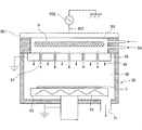
- FIG. 5 is a diagram for explaining an example of a film forming apparatus suitable for the present embodiment.
- FIG. 5 shows an apparatus related to RS-CVD (Radial Shower Chemical Vapor Deposition) that forms a film by using a vapor deposition method using radicals.
- the apparatus according to FIG. 5 has a vacuum vessel 50.
- the vacuum vessel 50 is exhausted by the exhaust system 51.
- the substrate 7 is carried into the vacuum vessel 50 from a gate valve (not shown) and is held by the substrate holder 53.
- the substrate holder 53 is maintained at a predetermined temperature by the heater 52.
- high-frequency power for example, 13.56 MHz
- a partition plate 56 made of a conductive member is disposed between the plasma generation chamber 55 and the radical reaction chamber 58, and the partition plate 56 has a through hole 57. Further, the partition plate 56 is provided with a second gas introduction system 59, and a raw material gas can be supplied to the radical reaction chamber 58.
- the plasma P contains electrons, radicals, and ions, but the electrons and ions are blocked by the partition plate 56 charged by high frequency discharge, and the radicals selectively pass through the through holes 57 and are introduced into the radical reaction chamber 58. Then, a source gas is also introduced from the second gas introduction system 59 of the partition plate 56 and is deposited on the substrate 7 to form a film.
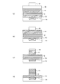
- FIG. 1 is a diagram schematically showing a method of manufacturing a magnetoresistive effect element according to this embodiment.
- FIG. 2 is a diagram schematically showing the structure of the magnetoresistive effect element according to this embodiment.
- FIG. 3 is a diagram schematically showing processing steps up to the multilayer film 12 in the manufacture of the magnetoresistive effect element according to the present embodiment.
- a wiring 14 (for example, Cu) is formed on a substrate such as silicon or glass, and is joined to the wiring 14 on the wiring 14.
- a base layer 13 to be a lower electrode is formed.
- a multilayer film 12 having a magnetic junction is formed on the underlayer 13.
- a cap layer 11 serving as an upper electrode is formed on the multilayer film 12.
- a hard mask (for example, SiO 2 ) 18 and a resist 19 for patterning the cap layer 11 are formed on the cap layer 11. The layer above the cap layer 11 is appropriately selected depending on the etching method and the etching target.
- the underlayer 13 is preferably a single layer film or a laminated film of tantalum, titanium, aluminum, silicon, ruthenium or a conductive compound thereof such as tantalum nitride, titanium nitride, ruthenium oxide, ruthenium nitride, tantalum carbide, and titanium carbide. is there.
- an antiferromagnetic layer 124, a magnetization fixed layer 123, a barrier layer 122, and a magnetization free layer 121 are laminated in order from the bottom.
- the cap layer 11 is processed into an upper electrode in a later step, a conductive material is used.
- the cap layer 11 is preferably a single-layer film or a laminated film of tantalum, titanium, or a conductive compound thereof such as tantalum nitride, titanium nitride, tantalum carbide, or titanium carbide.
- a base layer, a multilayer film, a cap layer, a hard mask for patterning, and a resist layered before patterning are referred to as “laminated structure” in the present invention.
- a multilayer film, a cap layer, a hard mask, and a resist that are processed by patterning to form a lower electrode are referred to as “magnetoresistance effect elements”.
- the “multilayer film” refers to a film having a basic structure in a functional element such as a magnetoresistive effect element.
- the above-described laminated structure is processed using, for example, the apparatus shown in FIGS. An example is shown in FIG.
- FIG. 3A shows a state in which the resist 19 is patterned. From this state, the pattern formed on the resist is transferred to the lower hard mask 18 by RIE using fluorocarbon as an etching gas.
- FIG. 3B shows a state in which the resist 19 is removed by ashing after patterning the hard mask 18.
- FIG. 3C shows a state where the pattern formed on the hard mask 18 is transferred to the cap layer 11 by RIE using a chlorine-based gas as an etching gas.
- FIG. 3D shows a state in which the multilayer film 12 is processed from this state by RIE using a carbon base gas such as alcohol as an etching gas, using the cap layer 11 as a mask.
- a carbon base gas such as alcohol
- the etching is stopped at the base layer 13 because the base layer 13 is difficult to be etched.
- the carbon base gas include alcohol (CH 3 OH, C 2 H 5 OH, etc.), and mixed gas obtained by adding oxygen or nitrogen to hydrocarbon (CH 4 + O 2 , C 2 H 6 + N 2 + O 2 , C 2 H 4). + O 2 or the like), a mixed gas of carbon monoxide and ammonia, carbon dioxide, or the like.
- FIG. 1 shows a method of manufacturing a magnetoresistive effect element according to the present invention.
- FIG. 1A shows a state after patterning up to the upper layer of the base layer 13 as described above.
- FIG. 1B shows a state in which the protective film 15 is formed on the base layer 13, the multilayer film 12, and the cap layer 11 from this state.
- Various methods such as a sputtering method and a CVD method are used for forming the protective film 15. From the viewpoint of securing a sufficient amount of film formation on the side walls of the cap layer 11 and the multilayer film 12, the CVD method is preferable.
- a sufficient protective film is formed on the sidewalls of the multilayer film 12 and the cap layer 11, and damage to the element during film formation can be reduced. .
- FIG. 1B shows the same state as FIG.1 (b), and is a figure for demonstrating the surface part 15a and the side wall part 15b.
- the surface portion 15a and the base layer 13 are etched using the protective film 15 as a mask.
- the state after this etching is shown in FIG.
- the upper electrode and the lower electrode are formed simultaneously.
- an IBE method, an RIE method, or the like is used.
- the RIE method is particularly preferable.
- the etching amount of the surface portion 15a and the underlayer 13 with respect to the etching amount of the side wall portion 15b is referred to as “anisotropic”. That is, the large anisotropy indicates that the etching amount of the surface portion 15a and the base layer 13 is large with respect to the etching amount of the side wall portion 15b.
- an insulating film is generally used to prevent an electrical short circuit.
- etching gas when etching is performed by the RIE method, various gases such as an inert gas such as Ar can be used.
- fluorocarbon and hydrofluorocarbon (hereinafter collectively referred to as CF-based gas) are preferable.
- CF 4 or C 2 F 6 is preferred as the fluorocarbon
- CHF 3 is preferred as the hydrofluorocarbon.
- CF-based gas the anisotropy can be increased, and a protective film is formed on the side wall portion 15b by the carbon polymer generated during etching. Therefore, the side wall portion 15b is processed during the processing of the underlayer 13. The possibility of disappearing can be reduced.
- the side wall portion 15b disappears during the processing of the surface portion 15a and the underlayer 13, there is a possibility that the conductive material of the underlayer 13 adheres to the side wall portion of the multilayer film 12 and is electrically short-circuited.
- argon, helium, nitrogen, hydrogen, oxygen, xenon, or the like may be added as an additive gas to the CF gas.
- anisotropy can be further increased by using a silicon-based insulating film such as silicon oxide or silicon nitride for the protective film 15.
- the base layer 13 does not need to be processed vertically as shown in FIG. 1D, and the base layer 13 between adjacent elements is etched to prevent an electrical short circuit. , May be tapered.
- the etching is performed using the protective film 15 as a mask, the upper electrode and the lower electrode are formed by one etching process. Further, since the protective film 15 formed on the patterned multilayer film 12 and the cap layer 11 also has a shape along the pattern, the use of the protective film 15 as a mask causes a problem of positional displacement of the lower electrode pattern. Can be prevented.
- the surface portion 15a and the underlayer 13 are etched using the protective film 15 as a mask, but this etching process may be composed of a plurality of steps.
- the source power may be increased at the beginning of etching and the source power may be continuously decreased toward the end of etching.
- the etching gas, the pressure in the processing space, the gas flow rate, the power supplied to the plasma generation unit, and the like can be changed.
- the above-described etching process may be performed by two or more processes according to the material of the protective film or the underlayer.
- the second etching step may be performed in a different processing space and different atmosphere from the first etching step. In this case, the number of etching steps is increased as compared with the present embodiment, but the problem of misalignment can be prevented.
- the formation of the protective film 15 and the subsequent etching are consistently performed in a vacuum.
- the protective film 15 may be taken out to the atmosphere and then etched using a different apparatus. .
- the protective film 15 was formed by the RS-CVD method under the following conditions using the apparatus shown in FIG.
- the source gases 1 and 2 are gases introduced from the first gas introduction system 54, and the source gas 3 is a gas introduced from the second gas introduction system 59.
- Source gas 1 SiH 4
- Source gas 2 Ar
- Source gas 3 NH 3
- Flow rate of source gas 1 110 mL / min (sccm)
- Flow rate of source gas 2 250 mL / min (sccm)
- Flow rate of source gas 3 2500 mL / min (sccm)
- Source power 1000W Pressure in the vacuum vessel 50: 20 Pa
- the temperature of the substrate holder holding the substrate 7 180 ° C.
- Etching gas CF 4 Etching gas flow rate: 50 mL / min (sccm)
- Source power 700W
- Bias power 50W
- the present invention can also be used in a method for manufacturing various functional elements such as a resistance change element (ReRAM) and a ferroelectric memory (FeRAM).
- these functional elements similarly to the present invention, after patterning the multilayer film having the basic structure of the functional element, a protective film covering the base layer and the multilayer film is formed, and the base layer is processed using the protective film as a mask. A lower electrode can be formed. Accordingly, when used for these functional elements, similarly, the number of steps in forming the lower electrode can be reduced, and displacement can be prevented.
- the basic structure here refers to a structure that is at least necessary for performing its function, such as a tunnel barrier layer and a pair of ferromagnetic layers that cause a magnetoresistive effect in a magnetoresistive element. .
- the present invention can be used in a method for manufacturing a functional element.
Landscapes
- Engineering & Computer Science (AREA)
- Computer Hardware Design (AREA)
- Manufacturing & Machinery (AREA)
- Hall/Mr Elements (AREA)
- Mram Or Spin Memory Techniques (AREA)
- Drying Of Semiconductors (AREA)
- Semiconductor Memories (AREA)
Abstract
Description
本実施形態を用いて磁気抵抗効果素子の製造を行った実施例を以下に示す。
原料ガス2:Ar
原料ガス3:NH3
原料ガス1の流量:110mL/min(sccm)
原料ガス2の流量:250mL/min(sccm)
原料ガス3の流量:2500mL/min(sccm)
ソース電力:1000W
真空容器50内の圧力:20Pa
基板7を保持する基板ホルダーの温度:180℃
エッチングガスの流量:50mL/min(sccm)
ソース電力:700W
バイアス電力:50W
真空容器30内の圧力:0.4Pa
基板7を保持する基板ホルダーの温度:80℃
12 多層膜
13 下地層
14 配線
15 保護膜
16 層間膜
17 マスク
18 ハードマスク
19 レジスト
7 基板
40 真空容器
401 プラズマ源
402 アンテナ
403 プラズマ用高周波電源
404 伝送路
405 磁石
406 誘導体壁容器
41 ガス導入系
42 磁石
43 排気系
44 基板ホルダー
45 温度制御
46 バイアス用高周波電源
50 真空容器
501 高周波電極
502 高周波電源
503 伝送路
51 排気系
52 ヒータ
53 基板ホルダー
54 第1のガス導入系
55 プラズマ生成室
56 隔壁板
57 貫通孔
58 ラジカル反応室
59 第2のガス導入系
Claims (6)
- 機能素子の製造方法であって、
下地層とパターニングされた多層膜及びキャップ層に保護膜を形成する保護膜形成工程と、
前記保護膜及び前記下地層の所定の領域をエッチングすることで上部電極及び下部電極を1の工程により形成する電極形成工程と、
を備えることを特徴とする機能素子の製造方法。 - 前記エッチングは反応性イオンエッチングであることを特徴とする請求項1に記載の機能素子の製造方法。
- 前記保護膜はCVD法により形成されることを特徴とする請求項2に記載の機能素子の製造方法。
- 前記保護膜は酸化シリコンもしくは窒化シリコンであり、
前記下地層はタンタル、チタン、アルミニウム、シリコン、ルテニウム、窒化タンタル、窒化チタン、酸化ルテニウム、窒化ルテニウム、炭化タンタル、炭化チタンのいずれかの単層膜または積層膜であることを特徴とする請求項3に記載の機能素子の製造方法。 - 前記キャップ層はタンタル、チタン、窒化タンタル、窒化チタン、炭化タンタル、炭化チタンのいずれかの単層膜又は積層膜であることを特徴とする請求項4に記載の機能素子の製造方法。
- 前記反応性イオンエッチングにおいてエッチングガスとしてフルオロカーボンもしくはハイドロフルオロカーボンを用いることを特徴とする請求項5に記載の機能素子の製造方法。
Priority Applications (3)
| Application Number | Priority Date | Filing Date | Title |
|---|---|---|---|
| JP2013521577A JP5689967B2 (ja) | 2011-06-24 | 2012-06-19 | 磁気抵抗効果素子の製造方法 |
| KR1020137030457A KR101574155B1 (ko) | 2011-06-24 | 2012-06-19 | 자기 저항 효과 소자의 제조 방법 |
| US14/128,722 US8970213B2 (en) | 2011-06-24 | 2012-06-19 | Method for manufacturing magnetoresistance effect element |
Applications Claiming Priority (2)
| Application Number | Priority Date | Filing Date | Title |
|---|---|---|---|
| JP2011-140392 | 2011-06-24 | ||
| JP2011140392 | 2011-06-24 |
Publications (1)
| Publication Number | Publication Date |
|---|---|
| WO2012176747A1 true WO2012176747A1 (ja) | 2012-12-27 |
Family
ID=47422583
Family Applications (1)
| Application Number | Title | Priority Date | Filing Date |
|---|---|---|---|
| PCT/JP2012/065562 Ceased WO2012176747A1 (ja) | 2011-06-24 | 2012-06-19 | 機能素子の製造方法 |
Country Status (4)
| Country | Link |
|---|---|
| US (1) | US8970213B2 (ja) |
| JP (1) | JP5689967B2 (ja) |
| KR (1) | KR101574155B1 (ja) |
| WO (1) | WO2012176747A1 (ja) |
Cited By (5)
| Publication number | Priority date | Publication date | Assignee | Title |
|---|---|---|---|---|
| JP2015018885A (ja) * | 2013-07-10 | 2015-01-29 | 株式会社日立ハイテクノロジーズ | プラズマエッチング方法 |
| JP2017228787A (ja) * | 2017-08-22 | 2017-12-28 | 株式会社日立ハイテクノロジーズ | プラズマエッチング方法 |
| WO2019188450A1 (ja) * | 2018-03-29 | 2019-10-03 | 東京エレクトロン株式会社 | エッチング方法 |
| US10833255B2 (en) | 2017-09-21 | 2020-11-10 | Hitachi High-Tech Corporation | Method for manufacturing magnetic tunnel junction element, and inductively coupled plasma processing apparatus |
| JP2024523775A (ja) * | 2021-06-16 | 2024-07-02 | インターナショナル・ビジネス・マシーンズ・コーポレーション | 側壁ポリマースペーサを有するワイドベース磁気トンネル接合デバイス |
Families Citing this family (11)
| Publication number | Priority date | Publication date | Assignee | Title |
|---|---|---|---|---|
| KR101566863B1 (ko) | 2011-08-25 | 2015-11-06 | 캐논 아네르바 가부시키가이샤 | 자기저항 소자의 제조 방법 및 자기저항 필름의 가공 방법 |
| WO2015045205A1 (ja) | 2013-09-25 | 2015-04-02 | キヤノンアネルバ株式会社 | 磁気抵抗効果素子の製造方法および製造システム |
| US10003014B2 (en) * | 2014-06-20 | 2018-06-19 | International Business Machines Corporation | Method of forming an on-pitch self-aligned hard mask for contact to a tunnel junction using ion beam etching |
| US10256395B2 (en) | 2015-06-19 | 2019-04-09 | Intel Corporation | Capped magnetic memory |
| US9771261B1 (en) * | 2016-03-17 | 2017-09-26 | Texas Instruments Incorporated | Selective patterning of an integrated fluxgate device |
| CN107623014A (zh) * | 2016-07-14 | 2018-01-23 | 上海磁宇信息科技有限公司 | 一种磁性随机存储器的制备方法 |
| JP2019047119A (ja) * | 2017-09-04 | 2019-03-22 | Tdk株式会社 | 磁気抵抗効果素子、磁気メモリ、および磁気デバイス |
| US10910560B2 (en) | 2018-09-21 | 2021-02-02 | Taiwan Semiconductor Manufacturing Co., Ltd. | RRAM structure |
| US11031543B2 (en) | 2018-10-23 | 2021-06-08 | Taiwan Semiconductor Manufacturing Co., Ltd. | Via landing enhancement for memory device |
| CN115734700B (zh) * | 2021-08-30 | 2025-11-11 | 江苏鲁汶仪器股份有限公司 | 一种mram磁隧道侧壁沾污的控制方法 |
| KR102809207B1 (ko) * | 2022-11-28 | 2025-05-16 | 세메스 주식회사 | 라이너 구조물 및 이를 포함하는 기판 처리 장치 |
Citations (3)
| Publication number | Priority date | Publication date | Assignee | Title |
|---|---|---|---|---|
| JP2005340260A (ja) * | 2004-05-24 | 2005-12-08 | Sony Corp | 磁性体層の加工方法および磁気記憶装置の製造方法 |
| JP2006179701A (ja) * | 2004-12-22 | 2006-07-06 | Toshiba Corp | 磁気ランダムアクセスメモリ |
| JP2009032872A (ja) * | 2007-07-26 | 2009-02-12 | Sharp Corp | 半導体装置の製造方法 |
Family Cites Families (7)
| Publication number | Priority date | Publication date | Assignee | Title |
|---|---|---|---|---|
| JP3951902B2 (ja) * | 2002-11-25 | 2007-08-01 | ヤマハ株式会社 | 磁気トンネル接合素子の製法と磁気トンネル接合装置 |
| JP2006060044A (ja) * | 2004-08-20 | 2006-03-02 | Canon Anelva Corp | 磁気抵抗効果素子の製造方法 |
| JP4534664B2 (ja) | 2004-08-24 | 2010-09-01 | ソニー株式会社 | 磁気記憶装置の製造方法 |
| JP2006261592A (ja) * | 2005-03-18 | 2006-09-28 | Fujitsu Ltd | 磁気抵抗効果素子及びその製造方法 |
| JP2008192222A (ja) * | 2007-02-02 | 2008-08-21 | Hitachi Global Storage Technologies Netherlands Bv | 磁気検出素子及びその製造方法 |
| TW201131644A (en) * | 2009-12-08 | 2011-09-16 | Ulvac Inc | Method of processing multilayer electrode |
| JP5720681B2 (ja) * | 2010-05-28 | 2015-05-20 | 日本電気株式会社 | 薄膜磁気デバイス及びその製造方法 |
-
2012
- 2012-06-19 JP JP2013521577A patent/JP5689967B2/ja active Active
- 2012-06-19 US US14/128,722 patent/US8970213B2/en active Active
- 2012-06-19 WO PCT/JP2012/065562 patent/WO2012176747A1/ja not_active Ceased
- 2012-06-19 KR KR1020137030457A patent/KR101574155B1/ko active Active
Patent Citations (3)
| Publication number | Priority date | Publication date | Assignee | Title |
|---|---|---|---|---|
| JP2005340260A (ja) * | 2004-05-24 | 2005-12-08 | Sony Corp | 磁性体層の加工方法および磁気記憶装置の製造方法 |
| JP2006179701A (ja) * | 2004-12-22 | 2006-07-06 | Toshiba Corp | 磁気ランダムアクセスメモリ |
| JP2009032872A (ja) * | 2007-07-26 | 2009-02-12 | Sharp Corp | 半導体装置の製造方法 |
Cited By (9)
| Publication number | Priority date | Publication date | Assignee | Title |
|---|---|---|---|---|
| JP2015018885A (ja) * | 2013-07-10 | 2015-01-29 | 株式会社日立ハイテクノロジーズ | プラズマエッチング方法 |
| US9680090B2 (en) | 2013-07-10 | 2017-06-13 | Hitachi High-Technologies Corporation | Plasma etching method |
| JP2017228787A (ja) * | 2017-08-22 | 2017-12-28 | 株式会社日立ハイテクノロジーズ | プラズマエッチング方法 |
| US10833255B2 (en) | 2017-09-21 | 2020-11-10 | Hitachi High-Tech Corporation | Method for manufacturing magnetic tunnel junction element, and inductively coupled plasma processing apparatus |
| WO2019188450A1 (ja) * | 2018-03-29 | 2019-10-03 | 東京エレクトロン株式会社 | エッチング方法 |
| JP2019176051A (ja) * | 2018-03-29 | 2019-10-10 | 東京エレクトロン株式会社 | エッチング方法 |
| JP7223507B2 (ja) | 2018-03-29 | 2023-02-16 | 東京エレクトロン株式会社 | エッチング方法 |
| US11616194B2 (en) | 2018-03-29 | 2023-03-28 | Tokyo Electron Limited | Etching method |
| JP2024523775A (ja) * | 2021-06-16 | 2024-07-02 | インターナショナル・ビジネス・マシーンズ・コーポレーション | 側壁ポリマースペーサを有するワイドベース磁気トンネル接合デバイス |
Also Published As
| Publication number | Publication date |
|---|---|
| JPWO2012176747A1 (ja) | 2015-02-23 |
| US8970213B2 (en) | 2015-03-03 |
| KR101574155B1 (ko) | 2015-12-03 |
| US20140138347A1 (en) | 2014-05-22 |
| JP5689967B2 (ja) | 2015-03-25 |
| KR20140007463A (ko) | 2014-01-17 |
Similar Documents
| Publication | Publication Date | Title |
|---|---|---|
| JP5689967B2 (ja) | 磁気抵抗効果素子の製造方法 | |
| US9601688B2 (en) | Method of manufacturing magnetoresistive element and method of processing magnetoresistive film | |
| US8546263B2 (en) | Method of patterning of magnetic tunnel junctions | |
| KR101066158B1 (ko) | 자기 소자의 제조 방법 및 제조 장치 | |
| US9577183B2 (en) | Methods of manufacturing a magnetoresistive random access memory device | |
| TW202006984A (zh) | 磁阻式隨機存取記憶體的製造方法及結構 | |
| KR101862632B1 (ko) | 자기 저항 효과 소자의 제조 방법 및 제조 시스템 | |
| US9647206B2 (en) | Method for etching layer to be etched | |
| KR20130015564A (ko) | 반도체 소자의 제조방법 | |
| CN103794717B (zh) | 一种包含介电层的嵌入型磁隧道结器件的制造方法 | |
| CN107623014A (zh) | 一种磁性随机存储器的制备方法 | |
| JP2025085021A (ja) | 側壁洗浄によるイオンビームエッチング | |
| TW201503257A (zh) | 電漿蝕刻方法 | |
| US20190019946A1 (en) | Methods for additive formation of a stt mram stack | |
| CN109994600A (zh) | 一种磁性随机存储器的制作方法 | |
| CN107658324A (zh) | 一种磁性隧道结的对准和形成方法 | |
| CN108232010B (zh) | 一种气体团簇离子束平坦化磁性隧道结底电极的方法 | |
| US20100301008A1 (en) | Process and apparatus for fabricating magnetic device | |
| CN111613571B (zh) | 一种制作磁性随机存储器单元阵列的方法 | |
| CN108242503B (zh) | 一种优化磁性隧道结的方法 | |
| JP5639195B2 (ja) | 電極膜の加工方法、磁性膜の加工方法、磁性膜を有する積層体、および該積層体の製造方法 | |
| US20150072440A1 (en) | Method of manufacturing magnetoresistive element | |
| CN114530550B (zh) | 一种mram磁隧道结的刻蚀方法 | |
| CN115666206A (zh) | 半导体结构及其制造方法、半导体存储器 | |
| CN111816224B (zh) | 一种磁性隧道结存储阵列单元及其外围电路的制备方法 |
Legal Events
| Date | Code | Title | Description |
|---|---|---|---|
| 121 | Ep: the epo has been informed by wipo that ep was designated in this application |
Ref document number: 12802871 Country of ref document: EP Kind code of ref document: A1 |
|
| DPE1 | Request for preliminary examination filed after expiration of 19th month from priority date (pct application filed from 20040101) | ||
| ENP | Entry into the national phase |
Ref document number: 20137030457 Country of ref document: KR Kind code of ref document: A |
|
| ENP | Entry into the national phase |
Ref document number: 2013521577 Country of ref document: JP Kind code of ref document: A |
|
| WWE | Wipo information: entry into national phase |
Ref document number: 14128722 Country of ref document: US |
|
| NENP | Non-entry into the national phase |
Ref country code: DE |
|
| 122 | Ep: pct application non-entry in european phase |
Ref document number: 12802871 Country of ref document: EP Kind code of ref document: A1 |