WO2012173019A1 - 投射型表示装置 - Google Patents
投射型表示装置 Download PDFInfo
- Publication number
- WO2012173019A1 WO2012173019A1 PCT/JP2012/064533 JP2012064533W WO2012173019A1 WO 2012173019 A1 WO2012173019 A1 WO 2012173019A1 JP 2012064533 W JP2012064533 W JP 2012064533W WO 2012173019 A1 WO2012173019 A1 WO 2012173019A1
- Authority
- WO
- WIPO (PCT)
- Prior art keywords
- conversion element
- polarization conversion
- polarized light
- light
- lens array
- Prior art date
- Legal status (The legal status is an assumption and is not a legal conclusion. Google has not performed a legal analysis and makes no representation as to the accuracy of the status listed.)
- Ceased
Links
Images




Classifications
-
- G—PHYSICS
- G03—PHOTOGRAPHY; CINEMATOGRAPHY; ANALOGOUS TECHNIQUES USING WAVES OTHER THAN OPTICAL WAVES; ELECTROGRAPHY; HOLOGRAPHY
- G03B—APPARATUS OR ARRANGEMENTS FOR TAKING PHOTOGRAPHS OR FOR PROJECTING OR VIEWING THEM; APPARATUS OR ARRANGEMENTS EMPLOYING ANALOGOUS TECHNIQUES USING WAVES OTHER THAN OPTICAL WAVES; ACCESSORIES THEREFOR
- G03B21/00—Projectors or projection-type viewers; Accessories therefor
- G03B21/14—Details
- G03B21/20—Lamp housings
- G03B21/2073—Polarisers in the lamp house
-
- G—PHYSICS
- G02—OPTICS
- G02B—OPTICAL ELEMENTS, SYSTEMS OR APPARATUS
- G02B27/00—Optical systems or apparatus not provided for by any of the groups G02B1/00 - G02B26/00, G02B30/00
- G02B27/28—Optical systems or apparatus not provided for by any of the groups G02B1/00 - G02B26/00, G02B30/00 for polarising
- G02B27/286—Optical systems or apparatus not provided for by any of the groups G02B1/00 - G02B26/00, G02B30/00 for polarising for controlling or changing the state of polarisation, e.g. transforming one polarisation state into another
-
- G—PHYSICS
- G02—OPTICS
- G02B—OPTICAL ELEMENTS, SYSTEMS OR APPARATUS
- G02B7/00—Mountings, adjusting means, or light-tight connections, for optical elements
- G02B7/003—Alignment of optical elements
- G02B7/005—Motorised alignment
-
- G—PHYSICS
- G02—OPTICS
- G02B—OPTICAL ELEMENTS, SYSTEMS OR APPARATUS
- G02B7/00—Mountings, adjusting means, or light-tight connections, for optical elements
- G02B7/008—Mountings, adjusting means, or light-tight connections, for optical elements with means for compensating for changes in temperature or for controlling the temperature; thermal stabilisation
-
- G—PHYSICS
- G03—PHOTOGRAPHY; CINEMATOGRAPHY; ANALOGOUS TECHNIQUES USING WAVES OTHER THAN OPTICAL WAVES; ELECTROGRAPHY; HOLOGRAPHY
- G03B—APPARATUS OR ARRANGEMENTS FOR TAKING PHOTOGRAPHS OR FOR PROJECTING OR VIEWING THEM; APPARATUS OR ARRANGEMENTS EMPLOYING ANALOGOUS TECHNIQUES USING WAVES OTHER THAN OPTICAL WAVES; ACCESSORIES THEREFOR
- G03B21/00—Projectors or projection-type viewers; Accessories therefor
- G03B21/14—Details
- G03B21/16—Cooling; Preventing overheating
-
- G—PHYSICS
- G03—PHOTOGRAPHY; CINEMATOGRAPHY; ANALOGOUS TECHNIQUES USING WAVES OTHER THAN OPTICAL WAVES; ELECTROGRAPHY; HOLOGRAPHY
- G03B—APPARATUS OR ARRANGEMENTS FOR TAKING PHOTOGRAPHS OR FOR PROJECTING OR VIEWING THEM; APPARATUS OR ARRANGEMENTS EMPLOYING ANALOGOUS TECHNIQUES USING WAVES OTHER THAN OPTICAL WAVES; ACCESSORIES THEREFOR
- G03B21/00—Projectors or projection-type viewers; Accessories therefor
- G03B21/14—Details
- G03B21/20—Lamp housings
- G03B21/208—Homogenising, shaping of the illumination light
-
- G—PHYSICS
- G02—OPTICS
- G02B—OPTICAL ELEMENTS, SYSTEMS OR APPARATUS
- G02B26/00—Optical devices or arrangements for the control of light using movable or deformable optical elements
Definitions
- the present invention relates to a projection display device that modulates incident light on a display element in accordance with a video signal, emits the light, and projects the emitted light onto a screen, and in particular, by a heat of a polarization conversion element.
- the present invention relates to a projection display device capable of suppressing deterioration.
- the polarization conversion element includes a polarization beam splitter (PBS) prism that separates indefinitely polarized incident light into a first polarization and a second polarization orthogonal to each other, and one of the first polarization and the second polarization. And a half-wave plate that converts the light into the other polarized light.
- PBS polarization beam splitter
- the polarization conversion element becomes a high temperature because it is a part where the light beam emitted from the light source is condensed.
- the PBS prism and the half-wave plate are bonded with an adhesive, and the PBS prism itself is also used for bonding a plurality of prisms.
- the adhesive deteriorates due to an oxidation process or a photochemical reaction process.
- the half-wave plate is made of polycarbonate, which is an organic material, the polycarbonate is relatively susceptible to heat and thus is likely to deteriorate. Therefore, the polarization conversion element is generally air-cooled by a cooling fan.
- an object of the present invention is to provide a projection display device capable of reducing deterioration of a polarization conversion element.
- a light source (LS) and a plurality of lens cells (4a) are two-dimensionally arranged, and the light source (LS)
- the first lens array (4) that splits the light beam emitted from the first lens array (4) and the plurality of lens cells (5a) corresponding to the plurality of lens cells (4a) in the first lens array (4) are two-dimensional.
- the second lens array (5) to which the light emitted from the first lens array (4) is incident, and the indefinite polarization emitted from the second lens array (5) are the first
- the first polarized light and the second polarized light are separated into the first polarized light and the first polarized light by converting the first polarized light into the second polarized light or converting the second polarized light into the first polarized light.
- Polarized light emitted in alignment with either one of the second polarized light The conversion element (6) and the polarization conversion element (6) are orthogonal to the polarization separation direction of the polarization conversion element (6) along the surface of the polarization conversion element (6) irradiated with the indefinite polarization.
- a projection display device comprising a drive mechanism (20) that is displaced in one direction.
- the projection display device of the present invention it is possible to reduce the deterioration of the polarization conversion element.
- FIG. 1 is a configuration diagram showing an embodiment of a projection display device of the present invention.
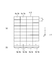
- FIG. 2 is a diagram showing a configuration example of the lens arrays 4 and 5 in FIG.
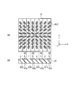
- FIG. 3 is a diagram illustrating a configuration example of the polarization conversion element 6 in FIG. 1.
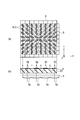
- FIG. 4 is a diagram showing a positional relationship between the lens array 5 and the polarization conversion element 6 in FIG.
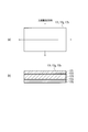
- FIG. 5 is a diagram showing a schematic configuration of the liquid crystal display elements 17b, 17g, and 17r in FIG.
- FIG. 6 is a diagram conceptually showing a state in which the illumination light emitted from the light source unit LS in FIG. 1 is superimposed on the liquid crystal display elements 17b, 17g, and 17r to form an image.
- FIG. 1 is a configuration diagram showing an embodiment of a projection display device of the present invention.
- FIG. 2 is a diagram showing a configuration example of the lens arrays 4 and 5 in FIG.
- FIG. 3 is a diagram illustrating
- FIG. 7 is a diagram illustrating a configuration example of the drive mechanism 20 in FIG.
- FIG. 8 is a diagram for explaining the displacement of the polarization conversion element 6 by the drive mechanism 20.
- FIG. 9 is a diagram illustrating a state of light irradiated on the polarization conversion element 6 due to the displacement of the polarization conversion element 6 by the driving mechanism 20.
- the light source LS includes a double-end type discharge lamp 1 and a reflector 2 that reflects light emitted from the discharge lamp 1 in the optical axis direction (Z direction).
- the discharge lamp 1 a lamp that emits white light such as a high-pressure mercury lamp or a metal halide lamp is used.
- the reflector 2 has a reflecting surface with a paraboloidal surface about the optical axis, reflects the light emitted from the discharge lamp 1 by the reflecting surface, and emits it as illumination light parallel to the optical axis.
- the reflector 2 may have a spheroidal reflecting surface with the optical axis as an axis. In that case, a lens system for making the illumination light substantially parallel light is provided on the light emission side of the reflector 2.
- the first lens array 4 includes rectangular lens cells 4a that are similar to display areas of reflective liquid crystal display elements 17b, 17g, and 17r described later. A plurality of arrays are arranged in the horizontal direction (X direction) and the vertical direction (Y direction). 2A is a front view of the first lens array 4 viewed in the Z direction, and FIG. 2B is a side view of the first lens array 4 viewed from the upper end surface.
- the pitch of the lens cells 4a in the vertical direction is H.
- the first lens array 4 is configured to spatially divide the aperture from which the reflector 2 emits a light beam. Illumination light emitted from the first lens array 4 enters the second lens array 5.
- the first and second lens arrays 4 and 5 are also referred to as a fly eye lens and a fly eye integrator.
- the second lens array 5 has the same configuration as the first lens array 4, and is similar to the display area of the liquid crystal display elements 17b, 17g, and 17r, as shown in FIGS.
- a plurality of rectangular lens cells 5a are arranged in the X and Y directions.
- the pitch of the lens cells 5a in the vertical direction is H.
- the first lens array 4 causes illumination light to enter the lens cells 5 a of the second lens array 5 corresponding to the plurality of lens cells 4 a in the first lens array 4, and the second lens array 5
- the same number of secondary light source images as the lens cells 4a of one lens array 4 are formed.
- the lens cells 4a and 5a are arranged in four rows in the X direction, but in reality there are more rows. The same applies to the number of rows in the Y direction.
- FIGS. 3A is a front view of the polarization conversion element 6 viewed in the Z direction
- FIG. 3B is a side view of the polarization conversion element 6 viewed from the upper end surface.
- the polarization conversion element 6 includes a PBS prism 61 and a half-wave plate 62.
- the PBS prism 61 is formed by joining a plurality of strip-shaped prisms each having a polarization separation surface 61a into a flat plate shape.
- the boundary between the strip-shaped prisms is a reflecting surface 61b.
- the P-polarized light passes through each polarization separation surface 61a and travels straight, and the S-polarized light is reflected by each polarization separation surface 61a and incident on the indefinite polarization.
- the traveling direction is bent by 90 °.
- a direction obtained by bending the traveling direction by 90 ° with respect to the incident direction of indefinite polarized light is the polarization separation direction.
- S-polarized light is reflected by the reflecting surface 61b and the traveling direction is further bent by 90 °.
- a half-wave plate 62 is adhered to the P-polarized light exit surface of the PBS prism 61. Accordingly, the P-polarized light emitted from the PBS prism 61 is converted into S-polarized light and emitted.
- the polarization conversion element 6 in the present embodiment emits indefinite polarized light that randomly includes P-polarized light and S-polarized light in alignment with the S-polarized light.
- the indefinite polarization may be aligned with the P polarization.
- the half-wave plate 62 is provided in a portion through which S polarized light reflected by the reflecting surface 61b passes.
- the cross hatched portion is a luminance concentration portion 6LC having a high light intensity when the illumination light emitted from the second lens array 5 is irradiated onto the polarization conversion element 6.
- each lens cell 5a of the second lens array 5 and the polarization conversion element 6 is as shown in FIGS. 4 (a) and 4 (b).
- the polarization conversion element 6 is positioned and arranged so that the center of each lens cell 5a is located at the center of the half-wave plate 62 in the X direction. Yes.
- the width of the lens cell 5 a in the X direction corresponds to the width of the two strip-shaped prisms in the polarization conversion element 6.
- the first and second lens arrays 4 and 5 and the polarization conversion element 6 are actually different in size and shifted in the center position.
- the outer dimensions are the same. Therefore, as shown in FIG. 1, the apparent outer dimensions of the first and second lens arrays 4 and 5 and the polarization conversion element 6 are the same.
- the S-polarized light emitted from the polarization conversion element 6 is incident on the overlapping lens 7.
- the superimposing lens 7 aligns the center of the image of each lens cell 4a of the first lens array 4 with the center of the liquid crystal display elements 17b, 17g, 17r, and converts the image of each lens cell 4a to the liquid crystal display elements 17b, 17g, It acts to form an image in an overlapping state on the display surface of 17r.
- the S-polarized light emitted from the overlapping lens 7 is separated into blue light and red / green light by the B / RG separation cross dichroic mirror 10.
- the optical path of the blue light is bent by the B mirror 11, passes through the blue field lens 14b, the blue wire grid PBS 15b, and the blue wavelength plate 16b, and enters the blue liquid crystal display element 17b.
- the P-polarized light modulated and reflected by the blue liquid crystal display element 17 b is reflected by the blue wire grid PBS 15 b and travels toward the cross dichroic prism 18.
- the red / green light separated by the B / RG separation cross dichroic mirror 10 is bent by the RG mirror 12.
- the red / green light is separated into red light and green light by the RG dichroic mirror 13.
- the red light passes through the red field lens 14r, the red wire grid PBS 15r, and the red wavelength plate 16r, and enters the red liquid crystal display element 17r.
- the P-polarized light modulated and reflected by the red liquid crystal display element 17r is reflected by the red wire grid PBS 15r and travels toward the cross dichroic prism 18.
- Green light passes through the green field lens 14g, the green wire grid PBS 15g, and the green wavelength plate 16g, and enters the green liquid crystal display element 17g.
- the P-polarized light modulated and reflected by the green liquid crystal display element 17g is reflected by the green wire grid PBS 15g and travels toward the cross dichroic prism 18.
- the cross dichroic prism 18 combines incident red light, blue light, and green light.
- the combined light is projected on the screen by the projection lens 19.
- the liquid crystal display elements 17b, 17g, and 17r for red, blue, and green modulate the incident red light, blue light, and green light according to the red component, blue component, and green component of the video signal.
- a projected image corresponding to the video signal is displayed on the screen.
- FIG. 5A is a plan view of the liquid crystal display elements 17b, 17g, and 17r
- FIG. 5B is a cross-sectional view of the liquid crystal display elements 17b, 17g, and 17r.
- the liquid crystal display elements 17b, 17g, and 17r include a transparent substrate 171 having a transparent electrode formed on a surface thereof and an active matrix substrate 175 having a reflective electrode for each pixel arranged in a matrix.
- the transparent electrode and the reflective electrode are opposed to face each other.
- the transparent substrate 171 side is the light incident side.
- a liquid crystal layer 173 in which nematic liquid crystal is sealed with a predetermined pretilt angle is provided.
- Alignment films 172 and 174 are formed on the surfaces of the transparent substrate 171 and the active matrix substrate 175 on the liquid crystal layer 173 side.
- the direction of incident polarized light is the horizontal direction on the plane of the liquid crystal display elements 17b, 17g, and 17r, as shown in FIG. Vertical direction.
- FIG. 6 conceptually illustrates a state in which an image is formed by being superimposed on the liquid crystal display elements 17b, 17g, and 17r through the lens 7.
- FIG. 2 conceptually illustrates a state in which an image is formed by being superimposed on the liquid crystal display elements 17b, 17g, and 17r through the lens 7.
- the light incident on the lens cell 4a of the first lens array 4 is condensed on the lens cell 5a of the second lens array 5 by the refractive power of each lens cell 4a, and the same number of secondary light source images as the lens cell 4a.
- the light emitted from the polarization conversion element 6 is superimposed on the liquid crystal display elements 17b, 17g, and 17r by the action of the superposing lens 7 to form an image.
- the light traveling in the direction (Z direction) orthogonal to the plane of the polarization conversion element 6 indicated by the alternate long and short dash line is collected at the center of the liquid crystal display elements 17b, 17g, and 17r.
- the light traveling in the direction inclined with respect to the direction orthogonal to the plane of the polarization conversion element 6 indicated by the broken line is condensed on the ends of the liquid crystal display elements 17b, 17g, and 17r.
- the light reflected by the reflecting surface 61b also includes light traveling in an inclined direction.
- only a part of the light passing in the inclined direction of the half-wave plate 62 is illustrated.
- the polarization conversion element 6 is displaced by the drive mechanism 20 in the Y direction, that is, in the longitudinal direction of the strip-shaped prism.
- the polarization conversion element 6 is accommodated in the housing 201.
- a leaf spring 202 as an example of an elastic member is attached to the upper end portion of the inner surface of the housing 201.
- a leaf spring 203 is also attached to one side of the inner surface of the housing 201 in the left-right direction (X direction).
- the upper end portion of the polarization conversion element 6 is in contact with the leaf spring 202, and a downward force is applied by the leaf spring 202.
- the lower end portion of the polarization conversion element 6 is in contact with the eccentric cam 204.
- the eccentric cam 204 is driven by a motor or the like (not shown) and rotates in the R direction.
- the polarization conversion element 6 is sandwiched between the leaf spring 202 and the eccentric cam 204.
- the eccentric cam 204 rotates, the position of the polarization conversion element 6 in the vertical direction (Y direction) is displaced.
- the state shown in FIG. 7 is a state in which the polarization conversion element 6 is located at the uppermost position.
- the leaf spring 203 presses the polarization conversion element 6 in the right direction in FIG. As a result, the position of the polarization conversion element 6 in the X direction is fixed.
- the second lens array 5 and the polarization conversion element 6 need to be accurately positioned in the X direction.
- the polarization conversion element 6 is positioned at a predetermined position in the X direction by pressing the polarization conversion element 6 against the inner surface of the housing 201 by the leaf spring 203.
- the polarization conversion element 6 is displaced in the Y direction, but does not affect the position in the X direction.
- FIG. 8A shows the positional relationship between the second lens array 5 and the polarization conversion element 6 in a state where the polarization conversion element 6 is located at the lowest position.
- the center position in the Y direction of the second lens array 5 and the center position in the Y direction of the polarization conversion element 6 are substantially the same position.
- This state is a first state in which the polarization conversion element 6 and the second lens array 5 are in a reference positional relationship.
- FIG. 8B shows the positional relationship between the second lens array 5 and the polarization conversion element 6 in a state where the polarization conversion element 6 is located at the uppermost position.
- the position of the polarization conversion element 6 in FIG. 8B is the position shown in FIG.
- the polarization conversion element 6 is pushed upward by the eccentric cam 204.
- a mechanism using the eccentric cam 204 as a mechanism for displacing the position of the polarization conversion element 6 has been described as an embodiment, the present invention is not limited to this.
- a mechanism for displacing the position of the polarization conversion element 6 for example, a mechanism may be used in which the position of the polarization conversion element 6 is displaced according to the amount of rotation of the lead screw using a lead screw.
- the following mechanism may be used.
- the light source LS As the light source LS is used, the light source LS gradually deteriorates and the amount of light emission decreases. As a result, the amount of light passing through the polarization conversion element 6 decreases, and the temperature around the polarization conversion element 6 decreases. Therefore, a leaf spring that presses the polarization conversion element 6 is formed of a shape memory alloy or bimetal whose elasticity and shape change depending on the temperature. The mechanism is such that the position of the polarization conversion element 6 is displaced according to the temperature of the leaf spring.
- the displacement direction of the polarization conversion element 6 is a direction along the surface irradiated with light in the polarization conversion element 6 and is one direction orthogonal to the polarization separation direction described with reference to FIG.
- the polarization conversion element 6 reaches the position shown in FIG. 8B, the light applied to the surface of the polarization conversion element 6 is displaced downward by H / 2.
- the drive mechanism 20 drives the polarization conversion element 6 so as to switch between the first state and the second state.
- the luminance concentration portion 6LC is in a state as shown in FIG.
- H / 2 the position of the luminance concentration part 6LC in the Y direction in FIG. 8A and the position of the luminance concentration part 6LC in the Y direction in FIG. It will be.
- the luminance concentration portion 6LC in FIG. 8B is located approximately between the luminance concentration portions 6LC in FIG. 8A in the Y direction. Accordingly, since the luminance concentration portion 6LC is always dispersed without being at the same position, the deterioration of the polarization conversion element 6 can be suppressed.
- the polarization conversion element 6 is selectively displaced in the Y direction between the position shown in FIG. 8A (first state) and the position shown in FIG. 8B (second state).
- the eccentric cam 204 is always rotated over a predetermined time
- the position of the polarization conversion element 6 in the Y direction is shown in FIG. 8A and FIG. 8B.
- the luminance concentration unit 6LC is connected to the Y direction.
- the displacement amount of the position of the polarization conversion element 6 is H / 2, but the present invention is not limited to this. What is necessary is just to displace the polarization conversion element 6 so that the location where light is always irradiated with respect to the polarization conversion element 6 may be reduced as much as possible. Of course, it is desirable to displace the polarization conversion element 6 so that there are no locations where light is constantly irradiated.
- the present invention is not limited to the embodiment described above, and various modifications can be made without departing from the scope of the present invention.
- the configuration using the reflective liquid crystal display elements 17b, 17g, and 17r as the display element is taken as an example, but a configuration using a transmissive liquid crystal display element may be used.
- the light source LS is not limited to a lamp, and may be any light emitting diode (LED), laser, excitation light source, or the like.
- the present invention can be used in any projection display device including a pair of lens arrays and a polarization conversion element.
Landscapes
- Physics & Mathematics (AREA)
- General Physics & Mathematics (AREA)
- Optics & Photonics (AREA)
- Projection Apparatus (AREA)
- Liquid Crystal (AREA)
- Transforming Electric Information Into Light Information (AREA)
Abstract
第1のレンズアレイ(4)は光源(LS)から発せられた光束を分割する。第2のレンズアレイ(5)は複数のレンズセルが二次元的に配置されて構成され、第1のレンズアレイ(4)から射出した光が入射される。偏光変換素子(6)は、第2のレンズアレイ(5)より射出した不定偏光をP偏光とS偏光とに分離し、P偏光とS偏光とのとのいずれか一方に揃えて射出する。駆動機構(20)は、偏光変換素子(6)を、偏光変換素子(6)の不定偏光が照射される面に沿って偏光分離方向と直交した方向に変位させる。
Description
本発明は、表示素子への入射光を映像信号に応じて変調して射出し、射出光をスクリーンに投射することによって映像を表示する投射型表示装置に係り、特に、偏光変換素子の熱による劣化を抑えることができる投射型表示装置に関する。
入射光を変調して射出する表示素子として液晶表示素子を用いた投射型表示装置が普及している。この種の投射型表示装置においては、液晶表示素子は偏光を入射光として利用するため、光源から射出した不定偏光を偏光変換素子によって第1の偏光と第2の偏光とのいずれか一方に揃えることにより、光の利用効率を高めるということが行われている。偏光変換素子は、不定偏光の入射光を互いに直交する第1の偏光と第2の偏光とに分離する偏光ビームスプリッタ(PBS)プリズムと、第1の偏光と第2の偏光とのいずれか一方を他方の偏光に変換する1/2波長板とを備える。
偏光変換素子は、光源から射出された光束が集光する部分であるため高温になる。PBSプリズムと1/2波長板は接着剤で接着され、PBSプリズム自体も複数のプリズムの接合に接着剤が用いられている。偏光変換素子に光束が集光して高温になると、接着剤が酸化プロセスや光化学反応プロセスにより劣化する。1/2波長板を有機材料であるポリカーボネート製とした場合には、ポリカーボネートは熱に比較的弱いため劣化しやすい。そこで、偏光変換素子を冷却ファンによって空冷するのが一般的である。
偏光変換素子を空冷しても、偏光変換素子が長期間に渡って高温になれば偏光変換素子は劣化し、信頼性に影響を与えることになる。これは、1/2波長板を特許文献1に記載されている比較的熱に強い水晶製としたとしても同様に発生する問題点である。そこで、偏光変換素子に光が集光して高温になることによる偏光変換素子の劣化を低減させることが求められている。
本発明はこのような要望に対応するため、偏光変換素子の劣化を低減させることができる投射型表示装置を提供することを目的とする。
本発明は、上述した従来の技術の課題を解決するため、本発明の一態様によれば、光源(LS)と、複数のレンズセル(4a)が二次元的に配置され、前記光源(LS)から発せられた光束を分割する第1のレンズアレイ(4)と、前記第1のレンズアレイ(4)における複数のレンズセル(4a)それぞれに対応する複数のレンズセル(5a)が二次元的に配置され、前記第1のレンズアレイ(4)から射出した光が入射される第2のレンズアレイ(5)と、前記第2のレンズアレイ(5)より射出した不定偏光を第1の偏光と第2の偏光とに分離すると共に、前記第1の偏光を前記第2の偏光に変換するか前記第2の偏光を前記第1の偏光に変換することにより前記第1の偏光と前記第2の偏光とのいずれか一方に揃えて射出する偏光変換素子(6)と、前記偏光変換素子(6)を、前記偏光変換素子(6)の前記不定偏光が照射される面に沿って、前記偏光変換素子(6)における偏光分離方向と直交した一の方向に変位させる駆動機構(20)とを備えることを特徴とする投射型表示装置が提供される。
本発明の投射型表示装置によれば、偏光変換素子の劣化を低減させることができる。
以下、本発明の投射型表示装置の一実施形態について、添付図面を参照して説明する。図1において、光源LSは、両口金タイプの放電灯1と、放電灯1から射出される光を光軸方向(Z方向)に反射するリフレクタ2を有する。放電灯1としては、高圧水銀ランプ、メタルハライドランプ等の白色光を射出するものが用いられる。リフレクタ2は、光軸を軸とした回転放物面の反射面を有し、放電灯1から射出された光を反射面で反射して光軸に平行な照明光として射出する。リフレクタ2は光軸を軸とした回転楕円面の反射面を有してもよい。その場合には、リフレクタ2の光の射出側に照明光をほぼ平行光とするレンズ系を設ける。
光源LSから射出した光は、紫外線や赤外線をカットするコールドフィルタ3を透過して第1のレンズアレイ4に入射される。第1のレンズアレイ4は、図2の(a),(b)に示すように、後述する反射型の液晶表示素子17b,17g,17rの表示領域と相似である矩形形状のレンズセル4aを水平方向(X方向)及び垂直方向(Y方向)に複数配列したものである。図2の(a)は第1のレンズアレイ4をZ方向に見た正面図、図2の(b)は上端面から見た側面図である。レンズセル4aの垂直方向のピッチはHである。
第1のレンズアレイ4は、リフレクタ2が光束を射出する開口を空間的に分割するように構成されている。第1のレンズアレイ4より射出した照明光は第2のレンズアレイ5に入射される。第1及び第2のレンズアレイ4,5はフライアイレンズ、フライアイインテグレータとも称される。
第2のレンズアレイ5は第1のレンズアレイ4と同様の構成であり、図2の(a),(b)に示すように、液晶表示素子17b,17g,17rの表示領域と相似である矩形形状のレンズセル5aをX方向及びY方向に複数配列したものである。レンズセル5aの垂直方向のピッチはHである。第1のレンズアレイ4は、第1のレンズアレイ4における複数のレンズセル4aそれぞれに対応した第2のレンズアレイ5のレンズセル5aに照明光を入射させ、第2のレンズアレイ5上に第1のレンズアレイ4のレンズセル4aと同数の2次光源像を形成する。なお、図2では、簡略化のため、レンズセル4a,5aのX方向の並びを4列としているが、実際にはさらに多くの列を有する。Y方向の行の数も同様である。
第2のレンズアレイ5から射出された照明光は、偏光変換素子6に入射される。図3の(a),(b)を用いて偏光変換素子6の構成及び作用について説明する。図3の(a)は偏光変換素子6をZ方向に見た正面図、図3の(b)は上端面から見た側面図である。図3の(b)に示すように、偏光変換素子6は、PBSプリズム61と1/2波長板62とを有する。PBSプリズム61は、偏光分離面61aが形成された複数の短冊状のプリズムを接合して平板状に形成したものである。短冊状のプリズムの境界は反射面61bとなっている。
本実施形態では、偏光変換素子6に入射される不定偏光の内、P偏光は各偏光分離面61aを透過して直進し、S偏光は各偏光分離面61aで反射して不定偏光の入射方向に対して進行方向が90°曲げられる。不定偏光の入射方向に対して進行方向を90°曲げた方向が偏光分離方向である。S偏光は反射面61bで反射してさらに進行方向が90°曲げられる。図3の(b)に示すように、PBSプリズム61のP偏光の射出面には、1/2波長板62が接着されている。従って、PBSプリズム61を射出したP偏光はS偏光に変換されて射出される。
即ち、本実施形態における偏光変換素子6は、P偏光及びS偏光をランダムに含む不定偏光をS偏光に揃えて射出するものである。不定偏光をP偏光に揃えるようにしてもよい。不定偏光をP偏光に揃える場合には、1/2波長板62を、反射面61bで反射したS偏光が通過する部分に設ける。図3の(a)において、クロスハッチングを付した部分は、第2のレンズアレイ5から射出された照明光が偏光変換素子6に照射されたときの光強度が強い輝度集中部6LCである。
第2のレンズアレイ5の各レンズセル5aと偏光変換素子6との具体的な位置関係は、図4の(a),(b)に示すようになっている。図4の(a),(b)に示すように、偏光変換素子6は、各レンズセル5aの中心が1/2波長板62のX方向の中心に位置するように位置決めされて配置されている。レンズセル5aのX方向の幅は、偏光変換素子6における短冊状のプリズム2列の幅に対応する。
図4の(a),(b)に示すように、第1及び第2のレンズアレイ4,5と偏光変換素子6とは実際には大きさが異なり、中心位置がずれている。これらの光学部品を筐体内に組み込む際に、外形寸法が同一となっていた方が都合がよい。そこで、図1に示すように、第1及び第2のレンズアレイ4,5と偏光変換素子6と見かけ上の外形寸法を同一としている。
図1において、偏光変換素子6から射出されたS偏光は、重ね合わせレンズ7に入射される。重ね合わせレンズ7は、第1のレンズアレイ4の各レンズセル4aの像の中心を液晶表示素子17b,17g,17rの中心に一致させ、各レンズセル4aの像を液晶表示素子17b,17g,17rの表示面上で重なり合った状態で結像させるように作用する。
重ね合わせレンズ7から射出されたS偏光は、B/RG分離クロスダイクロイックミラー10で青色光と赤色・緑色光とに分離される。青色光はBミラー11で光路が曲げられ、青色用フィールドレンズ14b,青色用ワイヤグリッドPBS15b,青色用波長板16bを通過し、青色用液晶表示素子17bに入射する。青色用液晶表示素子17bで変調され、反射したP偏光は青色用ワイヤグリッドPBS15bで反射して、クロスダイクロイックプリズム18へと向かう。
B/RG分離クロスダイクロイックミラー10で分離された赤色・緑色光はRGミラー12で光路が曲げられる。赤色・緑色光は、RGダイクロイックミラー13で赤色光と緑色光とに分離される。赤色光は、赤色用フィールドレンズ14r,赤色用ワイヤグリッドPBS15r,赤色用波長板16rを通過し、赤色用液晶表示素子17rに入射する。赤色用液晶表示素子17rで変調され、反射したP偏光は赤色用ワイヤグリッドPBS15rで反射して、クロスダイクロイックプリズム18へと向かう。
緑色光は、緑色用フィールドレンズ14g,緑色用ワイヤグリッドPBS15g,緑色用波長板16gを通過し、緑色用液晶表示素子17gに入射する。緑色用液晶表示素子17gで変調され、反射したP偏光は緑色用ワイヤグリッドPBS15gで反射して、クロスダイクロイックプリズム18へと向かう。
クロスダイクロイックプリズム18は、入射された赤色光,青色光,緑色光を合成する。合成光は投射レンズ19でスクリーン上に投射される。赤色用,青色用,緑色用の液晶表示素子17b,17g,17rは、入射された赤色光,青色光,緑色光それぞれを映像信号の赤色成分,青色成分,緑色成分に応じて変調するので、スクリーン上には映像信号に応じた投射画像が表示されることになる。
図5を用いて、液晶表示素子17b,17g,17rの概略構成について説明する。図5の(a)は液晶表示素子17b,17g,17rの平面図、図5の(b)は液晶表示素子17b,17g,17rの断面図である。図5の(b)に示すように、液晶表示素子17b,17g,17rは、表面に透明電極を形成した透明基板171と、画素毎の反射電極をマトリクス状に配置したアクティブマトリクス基板175とが、透明電極と反射電極とが向き合うように対向している。透明基板171側が光の入射側である。
透明基板171とアクティブマトリクス基板175との間には、例えばネマティック液晶が所定のプレチルト角を付与した状態で封入された液晶層173が設けられている。透明基板171とアクティブマトリクス基板175における液晶層173側の各表面には配向膜172,174が形成されている。
このように形成された液晶表示素子17b,17g,17rにおいて、入射される偏光の方向は、図5の(a)に示すように、液晶表示素子17b,17g,17rの平面上の水平方向または垂直方向である。
図6は、光源部LSから射出した照明光の光束が第1のレンズアレイ4によって複数のレンズセル4aによって分割され、分割された光束が第2のレンズアレイ5,偏光変換素子6,重ね合わせレンズ7を通って液晶表示素子17b,17g,17r上に重ね合わされて結像される状態を概念的に示している。
第1のレンズアレイ4のレンズセル4aに入射した光は、各レンズセル4aの屈折力によって第2のレンズアレイ5のレンズセル5a上に集光し、レンズセル4aと同数の2次光源像を形成する。偏光変換素子6より射出した光は重ね合わせレンズ7の作用によって液晶表示素子17b,17g,17r上に重ね合わされて結像する。
一点鎖線で示す偏光変換素子6の面と直交する方向(Z方向)に進む光は、液晶表示素子17b,17g,17rの中心に集光する。破線で示す偏光変換素子6の面と直交する方向に対して傾斜した方向に進む光は、液晶表示素子17b,17g,17rの端部に集光する。なお、反射面61bで反射した光も傾斜した方向に進む光を含むが、ここでは簡略化のため1/2波長板62を傾斜した方向で通過する光の一部のみを図示している。
図1に戻り、偏光変換素子6は駆動機構20によってY方向、即ち、短冊状のプリズムの長手方向に変位されるようになっている。
図7を用いて、駆動機構20の具体的構成例について説明する。図7に示すように、偏光変換素子6はハウジング201内に収納されている。ハウジング201の内面の上端部には、弾性部材としての一例である板ばね202が取り付けられている。ハウジング201の内面の左右方向(X方向)の一方の側にも、板ばね203が取り付けられている。
偏光変換素子6の上端部は板ばね202と接触しており、板ばね202によって下方への力が加えられている。偏光変換素子6の下端部は、偏心カム204と接触している。偏心カム204は図示していないモータ等によって駆動されてR方向に回転する。
偏光変換素子6は板ばね202と偏心カム204とによって挟まれており、偏心カム204が回転することによって、偏光変換素子6は上下方向(Y方向)の位置が変位することになる。図7に示す状態が、偏光変換素子6が最も上方に位置している状態である。板ばね203は、偏光変換素子6を図7の右方向に押圧している。これによって偏光変換素子6はX方向の位置が固定されている。
図4で説明したように、第2のレンズアレイ5と偏光変換素子6とはX方向に正確に位置決めされる必要がある。板ばね203によって偏光変換素子6をハウジング201の内面に押し付けることによって、偏光変換素子6はX方向の所定の位置に位置決めされる。なお、偏光変換素子6はY方向に変位するが、X方向の位置に影響を与えない。
図8の(a),(b)を用いて、偏光変換素子6のY方向の変位についてさらに説明する。図8の(a)は、偏光変換素子6が最も下方に位置している状態の第2のレンズアレイ5と偏光変換素子6との位置関係を示している。この状態で、第2のレンズアレイ5のY方向の中央位置と、偏光変換素子6のY方向の中央位置とはほぼ同じ位置にある。この状態を、偏光変換素子6と第2のレンズアレイ5とが基準の位置関係にある第1の状態とする。
図8の(b)は、偏光変換素子6が最も上方に位置している状態の第2のレンズアレイ5と偏光変換素子6との位置関係を示している。図8の(b)の偏光変換素子6の位置は図7に示す位置である。偏光変換素子6は偏心カム204によって上方に押し上げられている。
偏光変換素子6の位置を変位させる機構として偏心カム204を使用した機構を実施形態として示したが、これに限定されるものではない。偏光変換素子6の位置を変位させる他の機構として例えば、リードスクリューを使用してリードスクリューの回転量に応じて偏光変換素子6の位置が変位するような機構としてもよい。
また、次のような機構としてもよい。光源LSの使用時間に伴って、光源LSは徐々に劣化して発光量が減少する。これに伴って偏光変換素子6を通過する光量が減少し、偏光変換素子6周辺の温度が下がる。そこで、温度によって弾性や形状が変化する形状記憶合金やバイメタルで偏光変換素子6を押す板ばねを構成する。板ばねの温度に応じて偏光変換素子6の位置が変位するような機構とする。
図8の(a)の偏光変換素子6を最も下方に位置させた状態と図8の(b)の偏光変換素子6を最も上方に位置させた状態とで、偏光変換素子6を、垂直方向(Y方向)に、第2のレンズアレイ5におけるレンズセル5aの垂直方向のピッチHの1/2だけ変位させることが好ましい。偏光変換素子6の変位方向は、偏光変換素子6における光が照射される面に沿った方向で、図4の(b)で説明した偏光分離方向と直交する一の方向である。偏光変換素子6が図8の(b)の位置になると、偏光変換素子6の面に照射される光はH/2だけ下方へと変位する。
偏光変換素子6と第2のレンズアレイ5との一の方向の位置関係が、図8の(a)に示す第1の状態に対してH/2だけ変位した状態を第2の状態とする。駆動機構20は、第1の状態と第2の状態とを切り替えるように偏光変換素子6を駆動する。
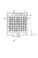
偏光変換素子6が図8の(a),(b)に示すように変位すると、輝度集中部6LCは図9に示すような状態となる。偏光変換素子6をH/2だけ変位させることによって、図8の(a)における輝度集中部6LCのY方向の位置と図8の(b)における輝度集中部6LCのY方向の位置とがずれることになる。図8の(b)の輝度集中部6LCはY方向でほぼ図8の(a)の輝度集中部6LCの間に位置することになる。従って、輝度集中部6LCが常時同じ位置にならず分散されるので、偏光変換素子6の劣化を抑えることが可能となる。
以上の説明では、偏光変換素子6をY方向に図8の(a)に示す位置(第1の状態)と図8の(b)に示す位置(第2の状態)とで選択的に変位させるように説明したが、偏心カム204を所定の時間をかけて常時回転させることにより、偏光変換素子6のY方向の位置を図8の(a)に示す位置と図8の(b)に示す位置との間で連続的に変化させるようにしてもよい。即ち、第1の状態から第2の状態へ、第2の状態から第1の状態へと所定の時間をかけて移行させるように、駆動機構20によって偏光変換素子6を連続的に駆動してもよい。偏光変換素子6のY方向の位置を連続的に変化させると、輝度集中部6LCはY方向につながったような状態となる。
また、本実施形態では偏光変換素子6の位置の変位量をH/2としたが、これに限定されるものではない。偏光変換素子6に対して光が常時照射される箇所がなるべく少なくなるように偏光変換素子6を変位させればよい。勿論、光が常時照射される箇所がなくなるように偏光変換素子6を変位させることが望ましい。
本発明は以上説明した本実施形態に限定されるものではなく、本発明の要旨を逸脱しない範囲において種々変更可能である。本実施形態では、表示素子として反射型の液晶表示素子17b,17g,17rを用いた構成を例にしたが、透過型の液晶表示素子を用いた構成としてもよい。光源LSとしては、ランプに限定されず、発光ダイオード(LED),レーザ,励起光源等、任意である。
本発明は、一対のレンズアレイと偏光変換素子とを備える任意の投射型表示装置において利用できる。
Claims (5)
- 光源と、
複数のレンズセルが二次元的に配置され、前記光源から発せられた光束を分割する第1のレンズアレイと、
前記第1のレンズアレイにおける複数のレンズセルそれぞれに対応する複数のレンズセルが二次元的に配置され、前記第1のレンズアレイから射出した光が入射される第2のレンズアレイと、
前記第2のレンズアレイより射出した不定偏光を第1の偏光と第2の偏光とに分離すると共に、前記第1の偏光を前記第2の偏光に変換するか前記第2の偏光を前記第1の偏光に変換することにより前記第1の偏光と前記第2の偏光とのいずれか一方に揃えて射出する偏光変換素子と、
前記偏光変換素子を、前記偏光変換素子の前記不定偏光が照射される面に沿って、前記偏光変換素子における偏光分離方向と直交した一の方向に変位させる駆動機構と、
を備えることを特徴とする投射型表示装置。 - 前記駆動機構は、前記偏光変換素子を、前記第2のレンズアレイにおける複数のレンズセルの前記一の方向のピッチの半分の距離だけ変位させることを特徴とする請求項1記載の投射型表示装置。
- 前記駆動機構は、前記偏光変換素子と前記第2のレンズアレイとの前記一の方向の位置関係が基準の位置関係にある第1の状態と、前記偏光変換素子と前記第2のレンズアレイとの前記一の方向の位置関係が、前記第1の状態に対して前記ピッチの半分の距離だけ変位した第2の状態とを切り替えるように、前記偏光変換素子を駆動することを特徴とする請求項2記載の投射型表示装置。
- 前記駆動機構は、前記第1の状態と前記第2の状態とを選択的に切り替えるように前記偏光変換素子を駆動することを特徴とする請求項3記載の投射型表示装置。
- 前記駆動機構は、前記第1の状態から前記第2の状態へ、前記第2の状態から前記第1の状態へと所定の時間をかけて移行させるように、前記偏光変換素子を連続的に駆動することを特徴とする請求項3記載の投射型表示装置。
Priority Applications (1)
| Application Number | Priority Date | Filing Date | Title |
|---|---|---|---|
| US13/799,378 US9470964B2 (en) | 2011-06-17 | 2013-03-13 | Projection display apparatus |
Applications Claiming Priority (4)
| Application Number | Priority Date | Filing Date | Title |
|---|---|---|---|
| JP2011135349 | 2011-06-17 | ||
| JP2011-135349 | 2011-06-17 | ||
| JP2012002869A JP5772606B2 (ja) | 2011-06-17 | 2012-01-11 | 投射型表示装置 |
| JP2012-002869 | 2012-01-11 |
Related Child Applications (1)
| Application Number | Title | Priority Date | Filing Date |
|---|---|---|---|
| US13/799,378 Continuation US9470964B2 (en) | 2011-06-17 | 2013-03-13 | Projection display apparatus |
Publications (1)
| Publication Number | Publication Date |
|---|---|
| WO2012173019A1 true WO2012173019A1 (ja) | 2012-12-20 |
Family
ID=47357008
Family Applications (1)
| Application Number | Title | Priority Date | Filing Date |
|---|---|---|---|
| PCT/JP2012/064533 Ceased WO2012173019A1 (ja) | 2011-06-17 | 2012-06-06 | 投射型表示装置 |
Country Status (3)
| Country | Link |
|---|---|
| US (1) | US9470964B2 (ja) |
| JP (1) | JP5772606B2 (ja) |
| WO (1) | WO2012173019A1 (ja) |
Citations (6)
| Publication number | Priority date | Publication date | Assignee | Title |
|---|---|---|---|---|
| JP2001228569A (ja) * | 2000-02-18 | 2001-08-24 | Fuji Photo Optical Co Ltd | 照明光学系およびこれを用いた投射型表示装置 |
| JP2003043419A (ja) * | 2001-07-30 | 2003-02-13 | Canon Inc | 偏光変換素子及びそれを用いた画像表示装置、投射型表示装置 |
| JP2004038096A (ja) * | 2002-07-08 | 2004-02-05 | Nec Viewtechnology Ltd | 偏光変換素子およびそれを備える液晶プロジェクタ |
| JP2007212496A (ja) * | 2006-02-07 | 2007-08-23 | Seiko Epson Corp | 光学装置及びプロジェクタ並びに光学装置の製造方法 |
| JP2010026403A (ja) * | 2008-07-23 | 2010-02-04 | Olympus Corp | 偏光変換装置およびそれを用いた画像投影装置 |
| JP2010204280A (ja) * | 2009-03-02 | 2010-09-16 | Canon Inc | 照明光学系及びそれを有する画像投射装置 |
Family Cites Families (9)
| Publication number | Priority date | Publication date | Assignee | Title |
|---|---|---|---|---|
| JP2001100699A (ja) * | 1999-09-29 | 2001-04-13 | Canon Inc | 投射型表示装置とその応用システム |
| JP2002214598A (ja) | 2001-01-22 | 2002-07-31 | Seiko Epson Corp | 液晶装置及びこれを用いたプロジェクタ |
| JP3797162B2 (ja) * | 2001-09-03 | 2006-07-12 | ソニー株式会社 | 投影装置 |
| JP2004118153A (ja) * | 2002-09-30 | 2004-04-15 | Mitsubishi Electric Corp | 投写型表示装置 |
| JP2004309853A (ja) | 2003-04-08 | 2004-11-04 | Sharp Corp | 液晶プロジェクタ |
| KR100608023B1 (ko) * | 2005-01-07 | 2006-08-02 | 삼성전자주식회사 | 하나의 프로젝터를 사용한 투사형 3차원 영상 디스플레이장치 |
| US8049822B2 (en) * | 2006-02-27 | 2011-11-01 | Sanyo Electric Co., Ltd. | Projection type video display |
| JP5263031B2 (ja) * | 2009-06-26 | 2013-08-14 | パナソニック株式会社 | 投写型表示装置 |
| JP5791118B2 (ja) * | 2010-12-21 | 2015-10-07 | Necディスプレイソリューションズ株式会社 | プロジェクタおよび画像表示方法 |
-
2012
- 2012-01-11 JP JP2012002869A patent/JP5772606B2/ja active Active
- 2012-06-06 WO PCT/JP2012/064533 patent/WO2012173019A1/ja not_active Ceased
-
2013
- 2013-03-13 US US13/799,378 patent/US9470964B2/en active Active
Patent Citations (6)
| Publication number | Priority date | Publication date | Assignee | Title |
|---|---|---|---|---|
| JP2001228569A (ja) * | 2000-02-18 | 2001-08-24 | Fuji Photo Optical Co Ltd | 照明光学系およびこれを用いた投射型表示装置 |
| JP2003043419A (ja) * | 2001-07-30 | 2003-02-13 | Canon Inc | 偏光変換素子及びそれを用いた画像表示装置、投射型表示装置 |
| JP2004038096A (ja) * | 2002-07-08 | 2004-02-05 | Nec Viewtechnology Ltd | 偏光変換素子およびそれを備える液晶プロジェクタ |
| JP2007212496A (ja) * | 2006-02-07 | 2007-08-23 | Seiko Epson Corp | 光学装置及びプロジェクタ並びに光学装置の製造方法 |
| JP2010026403A (ja) * | 2008-07-23 | 2010-02-04 | Olympus Corp | 偏光変換装置およびそれを用いた画像投影装置 |
| JP2010204280A (ja) * | 2009-03-02 | 2010-09-16 | Canon Inc | 照明光学系及びそれを有する画像投射装置 |
Also Published As
| Publication number | Publication date |
|---|---|
| JP5772606B2 (ja) | 2015-09-02 |
| US20130194549A1 (en) | 2013-08-01 |
| US9470964B2 (en) | 2016-10-18 |
| JP2013020222A (ja) | 2013-01-31 |
Similar Documents
| Publication | Publication Date | Title |
|---|---|---|
| JP5527058B2 (ja) | 光源装置及びプロジェクター | |
| JP5605047B2 (ja) | 光源装置およびそれを用いた投写型表示装置 | |
| TWI570500B (zh) | A light source device, a lighting device, and a projector | |
| US20110157566A1 (en) | Collimator lens unit, illuminating device, and projector | |
| CN102346366A (zh) | 投影机 | |
| CN108459454B (zh) | 照明装置和投影仪 | |
| JP5873625B2 (ja) | 光源装置及びプロジェクター | |
| US20130286360A1 (en) | Projector | |
| JP2012008303A (ja) | 光源装置及びそれを用いた投写型表示装置 | |
| JP2013080578A (ja) | 光源装置及びプロジェクター | |
| JP5672861B2 (ja) | プロジェクター | |
| JP2012063488A (ja) | 光源装置及びプロジェクター | |
| CN114265275A (zh) | 光源装置以及投影仪 | |
| WO2013098941A1 (ja) | 励起光合成ユニット、光源ユニットおよび投写型表示装置 | |
| JP7322691B2 (ja) | 光源装置およびプロジェクター | |
| JP6565365B2 (ja) | 光源装置、照明装置およびプロジェクター | |
| JP4382503B2 (ja) | 投写型表示装置の光源装置と投写型表示装置 | |
| JP5772606B2 (ja) | 投射型表示装置 | |
| JP2010169723A (ja) | プロジェクター | |
| JP7508964B2 (ja) | 光源装置およびプロジェクター | |
| JP2013222646A (ja) | 照明装置、電子機器及び投射型表示装置 | |
| JP5573025B2 (ja) | 照明光学系及びこの照明光学系を用いたプロジェクタ装置 | |
| CN114265272A (zh) | 光源装置以及投影仪 | |
| JP7131590B2 (ja) | 光源装置およびプロジェクター | |
| JP7484605B2 (ja) | 光源装置およびプロジェクター |
Legal Events
| Date | Code | Title | Description |
|---|---|---|---|
| 121 | Ep: the epo has been informed by wipo that ep was designated in this application |
Ref document number: 12800996 Country of ref document: EP Kind code of ref document: A1 |
|
| NENP | Non-entry into the national phase |
Ref country code: DE |
|
| 122 | Ep: pct application non-entry in european phase |
Ref document number: 12800996 Country of ref document: EP Kind code of ref document: A1 |