WO2012172985A1 - アクティブマトリクス基板の製造方法、アクティブマトリクス基板、表示装置、および、表示装置を備えたテレビジョン受像機 - Google Patents
アクティブマトリクス基板の製造方法、アクティブマトリクス基板、表示装置、および、表示装置を備えたテレビジョン受像機 Download PDFInfo
- Publication number
- WO2012172985A1 WO2012172985A1 PCT/JP2012/064061 JP2012064061W WO2012172985A1 WO 2012172985 A1 WO2012172985 A1 WO 2012172985A1 JP 2012064061 W JP2012064061 W JP 2012064061W WO 2012172985 A1 WO2012172985 A1 WO 2012172985A1
- Authority
- WO
- WIPO (PCT)
- Prior art keywords
- electrode
- source
- active matrix
- matrix substrate
- layer
- Prior art date
- Legal status (The legal status is an assumption and is not a legal conclusion. Google has not performed a legal analysis and makes no representation as to the accuracy of the status listed.)
- Ceased
Links
Images



















Classifications
-
- H—ELECTRICITY
- H10—SEMICONDUCTOR DEVICES; ELECTRIC SOLID-STATE DEVICES NOT OTHERWISE PROVIDED FOR
- H10D—INORGANIC ELECTRIC SEMICONDUCTOR DEVICES
- H10D86/00—Integrated devices formed in or on insulating or conducting substrates, e.g. formed in silicon-on-insulator [SOI] substrates or on stainless steel or glass substrates
- H10D86/40—Integrated devices formed in or on insulating or conducting substrates, e.g. formed in silicon-on-insulator [SOI] substrates or on stainless steel or glass substrates characterised by multiple TFTs
- H10D86/421—Integrated devices formed in or on insulating or conducting substrates, e.g. formed in silicon-on-insulator [SOI] substrates or on stainless steel or glass substrates characterised by multiple TFTs having a particular composition, shape or crystalline structure of the active layer
- H10D86/423—Integrated devices formed in or on insulating or conducting substrates, e.g. formed in silicon-on-insulator [SOI] substrates or on stainless steel or glass substrates characterised by multiple TFTs having a particular composition, shape or crystalline structure of the active layer comprising semiconductor materials not belonging to the Group IV, e.g. InGaZnO
-
- G—PHYSICS
- G02—OPTICS
- G02F—OPTICAL DEVICES OR ARRANGEMENTS FOR THE CONTROL OF LIGHT BY MODIFICATION OF THE OPTICAL PROPERTIES OF THE MEDIA OF THE ELEMENTS INVOLVED THEREIN; NON-LINEAR OPTICS; FREQUENCY-CHANGING OF LIGHT; OPTICAL LOGIC ELEMENTS; OPTICAL ANALOGUE/DIGITAL CONVERTERS
- G02F1/00—Devices or arrangements for the control of the intensity, colour, phase, polarisation or direction of light arriving from an independent light source, e.g. switching, gating or modulating; Non-linear optics
- G02F1/01—Devices or arrangements for the control of the intensity, colour, phase, polarisation or direction of light arriving from an independent light source, e.g. switching, gating or modulating; Non-linear optics for the control of the intensity, phase, polarisation or colour
- G02F1/13—Devices or arrangements for the control of the intensity, colour, phase, polarisation or direction of light arriving from an independent light source, e.g. switching, gating or modulating; Non-linear optics for the control of the intensity, phase, polarisation or colour based on liquid crystals, e.g. single liquid crystal display cells
- G02F1/133—Constructional arrangements; Operation of liquid crystal cells; Circuit arrangements
- G02F1/136—Liquid crystal cells structurally associated with a semi-conducting layer or substrate, e.g. cells forming part of an integrated circuit
- G02F1/1362—Active matrix addressed cells
- G02F1/1368—Active matrix addressed cells in which the switching element is a three-electrode device
-
- H—ELECTRICITY
- H10—SEMICONDUCTOR DEVICES; ELECTRIC SOLID-STATE DEVICES NOT OTHERWISE PROVIDED FOR
- H10D—INORGANIC ELECTRIC SEMICONDUCTOR DEVICES
- H10D86/00—Integrated devices formed in or on insulating or conducting substrates, e.g. formed in silicon-on-insulator [SOI] substrates or on stainless steel or glass substrates
- H10D86/01—Manufacture or treatment
- H10D86/021—Manufacture or treatment of multiple TFTs
- H10D86/0231—Manufacture or treatment of multiple TFTs using masks, e.g. half-tone masks
-
- H—ELECTRICITY
- H10—SEMICONDUCTOR DEVICES; ELECTRIC SOLID-STATE DEVICES NOT OTHERWISE PROVIDED FOR
- H10D—INORGANIC ELECTRIC SEMICONDUCTOR DEVICES
- H10D86/00—Integrated devices formed in or on insulating or conducting substrates, e.g. formed in silicon-on-insulator [SOI] substrates or on stainless steel or glass substrates
- H10D86/40—Integrated devices formed in or on insulating or conducting substrates, e.g. formed in silicon-on-insulator [SOI] substrates or on stainless steel or glass substrates characterised by multiple TFTs
- H10D86/60—Integrated devices formed in or on insulating or conducting substrates, e.g. formed in silicon-on-insulator [SOI] substrates or on stainless steel or glass substrates characterised by multiple TFTs wherein the TFTs are in active matrices
-
- H—ELECTRICITY
- H10—SEMICONDUCTOR DEVICES; ELECTRIC SOLID-STATE DEVICES NOT OTHERWISE PROVIDED FOR
- H10K—ORGANIC ELECTRIC SOLID-STATE DEVICES
- H10K59/00—Integrated devices, or assemblies of multiple devices, comprising at least one organic light-emitting element covered by group H10K50/00
- H10K59/10—OLED displays
- H10K59/12—Active-matrix OLED [AMOLED] displays
- H10K59/1201—Manufacture or treatment
-
- H—ELECTRICITY
- H10—SEMICONDUCTOR DEVICES; ELECTRIC SOLID-STATE DEVICES NOT OTHERWISE PROVIDED FOR
- H10K—ORGANIC ELECTRIC SOLID-STATE DEVICES
- H10K59/00—Integrated devices, or assemblies of multiple devices, comprising at least one organic light-emitting element covered by group H10K50/00
- H10K59/10—OLED displays
- H10K59/12—Active-matrix OLED [AMOLED] displays
- H10K59/121—Active-matrix OLED [AMOLED] displays characterised by the geometry or disposition of pixel elements
- H10K59/1213—Active-matrix OLED [AMOLED] displays characterised by the geometry or disposition of pixel elements the pixel elements being TFTs
-
- H—ELECTRICITY
- H10—SEMICONDUCTOR DEVICES; ELECTRIC SOLID-STATE DEVICES NOT OTHERWISE PROVIDED FOR
- H10K—ORGANIC ELECTRIC SOLID-STATE DEVICES
- H10K59/00—Integrated devices, or assemblies of multiple devices, comprising at least one organic light-emitting element covered by group H10K50/00
- H10K59/10—OLED displays
- H10K59/12—Active-matrix OLED [AMOLED] displays
- H10K59/123—Connection of the pixel electrodes to the thin film transistors [TFT]
-
- G—PHYSICS
- G02—OPTICS
- G02F—OPTICAL DEVICES OR ARRANGEMENTS FOR THE CONTROL OF LIGHT BY MODIFICATION OF THE OPTICAL PROPERTIES OF THE MEDIA OF THE ELEMENTS INVOLVED THEREIN; NON-LINEAR OPTICS; FREQUENCY-CHANGING OF LIGHT; OPTICAL LOGIC ELEMENTS; OPTICAL ANALOGUE/DIGITAL CONVERTERS
- G02F1/00—Devices or arrangements for the control of the intensity, colour, phase, polarisation or direction of light arriving from an independent light source, e.g. switching, gating or modulating; Non-linear optics
- G02F1/01—Devices or arrangements for the control of the intensity, colour, phase, polarisation or direction of light arriving from an independent light source, e.g. switching, gating or modulating; Non-linear optics for the control of the intensity, phase, polarisation or colour
- G02F1/13—Devices or arrangements for the control of the intensity, colour, phase, polarisation or direction of light arriving from an independent light source, e.g. switching, gating or modulating; Non-linear optics for the control of the intensity, phase, polarisation or colour based on liquid crystals, e.g. single liquid crystal display cells
- G02F1/133—Constructional arrangements; Operation of liquid crystal cells; Circuit arrangements
- G02F1/136—Liquid crystal cells structurally associated with a semi-conducting layer or substrate, e.g. cells forming part of an integrated circuit
- G02F1/1362—Active matrix addressed cells
- G02F1/136231—Active matrix addressed cells for reducing the number of lithographic steps
-
- H—ELECTRICITY
- H10—SEMICONDUCTOR DEVICES; ELECTRIC SOLID-STATE DEVICES NOT OTHERWISE PROVIDED FOR
- H10K—ORGANIC ELECTRIC SOLID-STATE DEVICES
- H10K59/00—Integrated devices, or assemblies of multiple devices, comprising at least one organic light-emitting element covered by group H10K50/00
- H10K59/10—OLED displays
- H10K59/12—Active-matrix OLED [AMOLED] displays
- H10K59/131—Interconnections, e.g. wiring lines or terminals
-
- H—ELECTRICITY
- H10—SEMICONDUCTOR DEVICES; ELECTRIC SOLID-STATE DEVICES NOT OTHERWISE PROVIDED FOR
- H10K—ORGANIC ELECTRIC SOLID-STATE DEVICES
- H10K59/00—Integrated devices, or assemblies of multiple devices, comprising at least one organic light-emitting element covered by group H10K50/00
- H10K59/80—Constructional details
- H10K59/805—Electrodes
- H10K59/8051—Anodes
Definitions
- the present invention relates to a method for manufacturing an active matrix substrate used in a liquid crystal display device, an organic EL (Electro Luminescence) display device, and the like, an active matrix substrate, a display device, and a television receiver including the display device.
- an organic EL Electro Luminescence
- Active matrix liquid crystal display devices and organic EL display devices are not only thin and have low power consumption, but also have characteristics such as a high contrast ratio and excellent response characteristics. For this reason, these display devices have come to be used as displays for televisions, notebook personal computers, portable terminals, and the like, and in recent years the market scale has been rapidly expanding.
- a plurality of scanning signal lines and a plurality of data signal lines intersecting with these scanning signal lines are formed via an insulating film.
- a pixel provided near the intersection of the scanning signal line and the data signal line is provided with a bottom gate type TFT (Thin Film Transistor) functioning as a switching element.
- TFT Thin Film Transistor
- Patent Document 1 discloses a manufacturing method of a bottom-gate TFT having a channel stop structure formed on an active matrix substrate. Specifically, after a gate electrode is formed by photolithography, a gate insulating film, a first semiconductor film, a second semiconductor film, and a second insulating film are formed in this order. A thick resist pattern and a thin resist pattern are formed on the second insulating film using a halftone mask. Using these resist patterns as a mask, the second insulating film, the second semiconductor film, and the first semiconductor film are etched in this order. Next, the thin resist pattern is removed by half etching. The second insulating film is further etched using the remaining thick resist pattern as a mask. Thereby, the first and second semiconductor layers and the channel protective layer are formed.
- a metal film for forming source / drain electrodes is formed, and the metal film is etched using a resist pattern newly formed on the metal film as a mask. Thereby, a source / drain electrode is formed. Further, using the same resist pattern as a mask, the channel protective layer and the second semiconductor layer are etched in this order. As a result, a contact layer is formed for ohmic connection between the source / drain electrode and the first semiconductor layer.
- the step of forming the gate electrode the step of forming the first and second semiconductor layers and the channel protective layer, and the step of forming the source / drain electrodes.
- a bottom gate TFT having stable electrical characteristics can be manufactured by forming resist patterns once, for a total of three times.
- Patent Document 1 discloses a method for manufacturing a TFT in which the manufacturing process is shortened by using a halftone mask.
- a method for manufacturing an active matrix substrate including not only TFTs but also terminals and wirings for supplying various control signals and image signals to the TFTs.
- the TFT manufacturing process can be shortened by using a halftone mask, if a new photolithography process is required to form terminals and wiring, the manufacturing cost of the active matrix substrate is reduced. Get higher.
- Patent Document 1 after the TFT is formed, a pixel contact is opened in the passivation film by a fourth photolithography process, and connected to the drain electrode through the pixel contact by a fifth photolithography process.
- the photolithography process requires a lot of manufacturing equipment in the manufacturing process. For this reason, if the number of times increases, the photolithography process becomes a bottleneck, and the productivity of the active matrix substrate decreases. If a manufacturing facility is added in order to improve productivity in the photolithography process, the cost for that will be needed, and the problem that the manufacturing cost of an active matrix substrate becomes high will arise.
- a scanning signal line, a data signal line intersecting with the scanning signal line, a pixel electrode, a gate electrode in the scanning signal line, a source electrode in the data signal line, and the pixel A first thin film transistor having a drain electrode electrically connected to the electrode, a gate lead line electrically connected to the scanning signal line, a source lead line electrically connected to the data signal line, A method of manufacturing an active matrix substrate comprising a drain lead line electrically connected to the pixel electrode on an insulating substrate, A first step of forming the scanning signal line, the gate electrode, and a first processed layer to be the pixel electrode; A second step of forming a first insulating film on the insulating substrate including the scanning signal line, the gate electrode, and the first processed layer; The pixel electrode is formed by etching the first processed layer using the first resist pattern formed at the same time and the second resist pattern having a film thickness thicker than the first resist pattern as a mask. And a third step of forming a semiconductor
- a gate terminal for applying an electrical signal to the scanning signal line from the outside via the gate lead line, and a source lead line from the outside.
- a source terminal for applying an electrical signal to the data signal line The first step further includes a step of forming a second processing layer to be a gate terminal electrode of the gate terminal and a third processing layer to be a source terminal electrode of the source terminal, The third step includes a step of etching the second and third processed layers to form the gate terminal electrode and the source terminal electrode, respectively.
- the first thin film transistor is a top contact thin film transistor
- the second step includes Forming a semiconductor film on the first insulating film; Forming a second insulating film on the semiconductor film,
- the third step includes Forming the pixel electrode and the gate lead line by sequentially etching the second insulating film and the semiconductor film using the first and second resist patterns as a mask; Removing the first resist pattern;
- the method further includes forming the first protective layer and the semiconductor layer by sequentially etching the second insulating film and the semiconductor film using the second resist pattern as a mask. To do.
- the fourth step includes Forming a source metal film so as to cover the first insulating film including the first protective layer and the semiconductor layer; Forming a third resist pattern on the source metal film; Etching the source metal film using the third resist pattern as a mask to form the source electrode, the drain electrode, the data signal line, the source lead line, and the drain lead line. It is characterized by including.
- a storage capacitor forming portion including an electrode layer and a storage capacitor wiring disposed on the insulating substrate with the first insulating film interposed therebetween, and a predetermined voltage from the outside via a storage capacitor wiring terminal.
- a storage capacitor wiring trunk for supplying to the storage capacitor, and a first contact portion for electrically connecting the storage capacitor wiring and the storage capacitor wiring trunk,
- the third step further includes a step of forming the first contact portion having a contact hole opened on the storage capacitor wiring trunk
- the fourth step further includes a step of forming the storage capacitor wiring electrically connected to the storage capacitor wiring trunk in the first contact portion by etching the source metal film.
- a sixth aspect of the present invention is the fourth aspect of the present invention, A light emitting layer; a second thin film transistor electrically connected to the light emitting layer; a supply line for applying a predetermined voltage to the second thin film transistor; and a predetermined voltage from the outside via a supply line terminal. And a second contact portion for electrically connecting the supply line and the supply line trunk,
- the third step further includes a step of forming the second contact portion having a contact hole opened on the supply line trunk using the first and second resist patterns as a mask,
- the fourth step includes a step of forming the supply line electrically connected to the supply line trunk in the second contact portion by etching the source metal film.
- the source metal film is a laminated metal film in which a plurality of metal films are laminated, and the metal film on the surface of the laminated metal film is a titanium film or a metal film containing titanium as a main component.
- the fourth step further includes a step of forming a second protective layer on each of the source electrode, the drain electrode, the data signal line, the source lead line, and the drain lead line.
- the fourth step further includes a step of covering the first thin film transistor, the gate lead line, and the source lead line and forming an interlayer insulating layer having an opening on the pixel electrode. To do.
- the first thin film transistor is a bottom contact type thin film transistor
- the second step further includes a step of forming a source metal film so as to cover the first insulating film
- the third step includes Etching the source metal film using the first and second resist patterns as a mask to form the pixel electrode; Removing the first resist pattern; Etching the source metal film using the second resist pattern as a mask to form the source electrode, the drain electrode, the data signal line, the source lead line, and the drain lead line. Is further included.
- a twelfth aspect of the present invention is the eleventh aspect of the present invention, After the third step, further comprising a fourth step,
- the fourth step includes Forming a semiconductor film on the first insulating film sandwiched between the source electrode and the drain electrode; Forming a second insulating film on the semiconductor film; Forming a third resist pattern on the second insulating film; Forming the first protective layer and the semiconductor layer by sequentially etching the second insulating film and the semiconductor film using the third resist pattern as a mask. To do.
- a thirteenth aspect of the present invention is the twelfth aspect of the present invention, A first connection electrode that electrically connects the drain lead line and the pixel electrode; and a second connection electrode that electrically connects the source lead line and the source terminal;
- the first connection electrode and the second connection electrode are formed by sequentially etching the second insulating film and the semiconductor film using the third resist pattern as a mask.
- the method further includes the step of:
- a fourteenth aspect of the present invention is the twelfth aspect of the present invention,
- the fourth step further includes a step of forming a second protective layer on the surfaces of the first and second connection electrodes.
- the semiconductor layer is made of an oxide semiconductor.
- a scanning signal line intersecting the scanning signal line, a pixel electrode, a gate electrode in the scanning signal line, a source electrode in the data signal line, and the pixel.
- a first thin film transistor having a drain electrode electrically connected to the electrode, a gate lead line electrically connected to the scanning signal line, a gate terminal electrically connected to the gate lead line, A source lead line electrically connected to the data signal line, a source terminal electrically connected to the source lead line, and a drain lead line electrically connected to the pixel electrode are provided on an insulating substrate.
- the gate terminal electrode of the gate terminal, the source terminal electrode of the source terminal, and the pixel electrode are made of the same metal film,
- the data signal line, the source lead line, and the drain lead line are made of the same metal film as the source electrode and the drain electrode.
- a seventeenth aspect of the present invention is the sixteenth aspect of the present invention,
- the gate terminal electrode and the source terminal electrode are surrounded by a first conductive layer having a higher conductivity than the metal film constituting them.
- a second electrode made of the same metal film as the first conductive layer is electrically connected to the first conductive layer on the surface of the gate terminal electrode and the source terminal electrode surrounded by the first conductive layer.
- a conductive layer is further formed.
- the nineteenth aspect of the present invention is the eighteenth aspect of the present invention,
- the second conductive layer is formed in a lattice shape on the gate terminal electrode and the source terminal electrode, respectively.
- the first thin film transistor includes a semiconductor layer having a lower surface electrically connected to an upper surface of the source electrode and the drain electrode,
- the drain lead line is electrically connected to the pixel electrode by a first connection electrode made of the same semiconductor film as the semiconductor layer,
- the source lead line is electrically connected to the source terminal electrode by a second connection electrode made of the semiconductor film.
- the 21st aspect of the present invention is the 16th aspect of the present invention, A light emitting layer; a second thin film transistor electrically connected to the light emitting layer; a supply line for applying a predetermined voltage to the second thin film transistor; and a predetermined voltage from the outside via a supply line terminal. And a contact portion for electrically connecting the supply line and the supply line trunk to each other.
- a twenty-second aspect of the present invention is a display device including the active matrix substrate according to any of the sixteenth to seventeenth aspects of the present invention.
- a twenty-third aspect of the present invention is a television receiver including the display device according to the twenty-second aspect of the present invention and a tuner unit that receives a television broadcast.
- the first resist pattern formed at the same time and the second resist pattern having a film thickness thicker than the first resist pattern are used as a mask.
- the semiconductor layer and the first protective layer of the first thin film transistor, or the source electrode and the drain electrode can be formed, and the pixel electrode can also be formed.
- the manufacturing process of the active matrix substrate can be shortened accordingly. Thereby, the manufacturing cost of the active matrix substrate can be reduced.
- the gate terminal electrode and the source terminal electrode can be formed simultaneously with the pixel electrode.
- the manufacturing process of the active matrix substrate can be further shortened, and the manufacturing cost can be further reduced.
- the top gate type first thin film transistor forms the pixel electrode and the gate lead line by etching using the first resist pattern and the second resist pattern as a mask. .
- the first resist pattern is removed, and etching is performed using the remaining second resist pattern as a mask, whereby the first protective layer and the semiconductor layer of the first thin film transistor are formed.
- the manufacturing cost of the active matrix substrate including the top contact type first thin film transistor can be further reduced.
- etching is performed using the third resist pattern as a mask, so that the source electrode, the drain electrode, the data signal, A line, a drain lead line, and a source lead line are formed simultaneously.
- the active matrix substrate includes the storage capacitor forming portion
- the first contact portion together with the source electrode and the like.
- a storage capacitor wiring electrically connected to the storage capacitor wiring trunk is formed.
- the source electrode and the like are supplied at the second contact portion.
- a supply line electrically connected to the trunk is formed.
- the source metal film is composed of a laminated metal film, titanium or a metal film mainly composed of titanium is formed on the surface of the laminated metal film,
- the corrosion resistance of the laminated metal film can be increased. For this reason, the reliability of the active matrix substrate can be increased.
- the corrosion resistance can be increased by forming the second protective layer on the surface of the source electrode, the drain electrode and the like. For this reason, the reliability of the active matrix substrate can be increased.
- the ninth aspect of the present invention by covering the first thin film transistor, the gate lead line, and the source lead line with the interlayer insulating layer, it is possible to increase their reliability.
- the second protective layer is unnecessary by covering with the interlayer insulating layer, the manufacturing cost of the active matrix substrate can be reduced.
- etching is performed using the second resist pattern as a mask so that the peripheral portion of the semiconductor layer protrudes from the edge of the first protective layer. Accordingly, a step that increases the reliability of electrical connection between the source and drain electrodes and the semiconductor layer can be formed without adding a new photolithography process. For this reason, the manufacturing cost of the active matrix substrate can be reduced.
- the pixel electrode is formed by etching using the first resist pattern and the second resist pattern as a mask.
- the first resist pattern is removed, and etching is performed using the remaining second resist pattern as a mask, thereby forming a source electrode, a drain electrode, and the like of the first thin film transistor.
- the source electrode, the drain electrode, and the like can be formed in one photolithography process, but also the pixel electrode can be formed. Thereby, the manufacturing cost of the active matrix substrate including the bottom contact type first thin film transistor can be further reduced.
- the first protective layer and the semiconductor layer of the first thin film transistor are simultaneously formed by etching using the third resist pattern as a mask.
- the first connection electrode and the second connection electrode are formed by etching using the third resist pattern as a mask.
- the manufacturing cost of the active matrix substrate can be reduced. Even in such a shortened manufacturing process, the drain lead line and the pixel electrode, and the source lead line and the source terminal can be reliably connected.
- the corrosion resistance can be increased by forming the second protective layer on the surfaces of the first connection electrode and the second connection electrode. For this reason, the reliability of the active matrix substrate can be increased.
- the manufacturing cost of the active matrix substrate including the first thin film transistor whose semiconductor layer is made of an oxide semiconductor can be reduced.
- the gate terminal electrode, the source terminal electrode, and the pixel electrode are made of the same metal film, and the data signal line, the source lead line, and the drain lead line are connected to the source electrode and the drain electrode, respectively. It consists of the same metal film.
- the constituent elements made of the same metal film are formed by etching using the resist pattern formed in the same photolithography process as a mask, the manufacturing process of the active matrix substrate can be shortened. Thereby, the manufacturing cost of the active matrix substrate can be reduced.
- the gate terminal electrode of the gate terminal and the source terminal electrode of the source terminal are surrounded by the first conductive layer made of the metal film having higher conductivity than the metal film constituting the gate terminal electrode. Is surrounded.
- the waveform deterioration of the electric signal input from the outside through the conductive particles contained in the anisotropic conductive film is suppressed.
- the second conductive layer made of the same metal film as the first conductive layer is further formed on the surfaces of the gate terminal electrode and the source terminal electrode.
- the second conductive layer is formed in a lattice pattern on the surfaces of the gate terminal electrode and the source terminal electrode.
- the first and second connection electrodes are made of a semiconductor film, they can be formed simultaneously with the formation of the semiconductor layer of the first thin film transistor.
- the first and second connection electrodes can be formed without adding a new manufacturing process, the manufacturing cost of the active matrix substrate can be reduced.
- the manufacturing process of the active matrix substrate used in the organic EL display device can be shortened. Thereby, the manufacturing cost of the active matrix substrate used for the organic EL display device can be reduced.
- the manufacturing cost of the display device can be reduced.
- the manufacturing cost of the television receiver can be reduced.
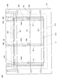
- FIG. 2 is a plan view showing a configuration of an active matrix substrate included in the liquid crystal display device shown in FIG. 1.
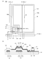
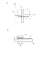
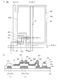
- (A) is an enlarged plan view showing a configuration of a pixel formed on the active matrix substrate shown in FIG. 2, and
- (b) is a cross-sectional view of the pixel along the line BB shown in (a).
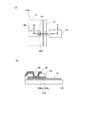
- FIG. 3A is a plan view showing a configuration of a gate terminal formed on the active matrix substrate shown in FIG. 2, and FIG.
- FIG. 3B is a cross-sectional view of the gate terminal along the line CC shown in FIG.
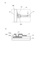
- FIG. 3A is a plan view showing a configuration of a source terminal formed on the active matrix substrate shown in FIG. 2
- FIG. 3B is a cross-sectional view of the source terminal along the line DD shown in FIG.
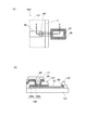
- (A) is a plan view showing a configuration of a contact portion formed on the active matrix substrate shown in FIG. 2
- (b) is a cross-sectional view of the contact portion along the line EE shown in (a).
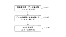
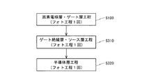
- 3 is a flowchart showing manufacturing steps of the active matrix substrate shown in FIG. 8 is a flowchart showing a detailed manufacturing process of a gate insulating layer / semiconductor layer process among the manufacturing processes of the active matrix substrate shown in FIG. 7.
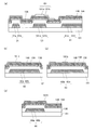
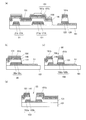
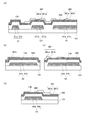
- FIG. 4A is a process sectional view of the pixel along the line BB shown in FIG. 3A
- FIG. 4B is a process sectional view of the gate terminal along the line CC shown in FIG.
- FIG. 5C is a process cross-sectional view of the source terminal along the line DD shown in FIG. 5A
- FIG. 6D is a contact portion along the line EE shown in FIG.
- FIG. 4A is a process sectional view of the pixel along the line BB shown in FIG. 3A
- FIG. 4B is a process sectional view of the gate terminal along the line CC shown in FIG.
- FIG. 5C is a process cross-sectional view of the source terminal along the line DD shown in FIG. 5A
- FIG. 6D is a contact portion along the line EE shown in FIG.
- FIG. 4A is a process sectional view of the pixel along the line BB shown in FIG. 3A
- FIG. 4B is a process sectional view of the gate terminal along the line CC shown in FIG.
- FIG. 5C is a process cross-sectional view of the source terminal along the line DD shown in FIG. 5A
- FIG. 6D is a contact portion along the line EE shown in FIG.
- FIG. FIG. 4A is a process sectional view of the pixel along the line BB shown in FIG. 3A
- FIG. 4B is a process sectional view of the gate terminal along the line CC shown in FIG. FIG.
- FIG. 5C is a process cross-sectional view of the source terminal along the line DD shown in FIG. 5A
- FIG. 6D is a contact portion along the line EE shown in FIG.
- FIG. 4A is a process sectional view of the pixel along the line BB shown in FIG. 3A
- FIG. 4B is a process sectional view of the gate terminal along the line CC shown in FIG.
- FIG. 5C is a process cross-sectional view of the source terminal along the line DD shown in FIG. 5A
- FIG. 6D is a contact portion along the line EE shown in FIG.
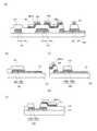
- FIG. FIG. 4A is a process sectional view of the pixel along the line BB shown in FIG. 3A
- FIG. 4B is a process sectional view of the gate terminal along the line CC shown in FIG.
- FIG. 5C is a process cross-sectional view of the source terminal along the line DD shown in FIG. 5A
- FIG. 6D is a contact portion along the line EE shown in FIG.
- FIGS. 13A to 13E are process cross-sectional views showing changes in shape when the channel protective layer and the semiconductor layer of the TFT shown in FIG. 12 are formed by a dry etching method.
- (A) is an enlarged plan view showing a configuration of a pixel formed on an active matrix substrate included in a modification of the liquid crystal display device according to the first embodiment
- (b) is an FF shown in (a). It is sectional drawing of the pixel along a line.
- (A) is a top view which shows the structure of the gate terminal formed in the active matrix substrate contained in the modification of the liquid crystal display device which concerns on 1st Embodiment, (b) is GG shown to (a). It is sectional drawing of the gate terminal along a line.
- (A) is a top view which shows the structure of the source terminal formed in the active matrix substrate included in the modification of the liquid crystal display device which concerns on 1st Embodiment, (b) is HH shown to (a). It is sectional drawing of the source terminal along a line.
- (A) is a top view which shows the structure of the contact part formed in the active matrix substrate contained in the modification of the liquid crystal display device which concerns on 1st Embodiment, (b) is II shown to (a).
- (A) is a plan view showing a configuration of a modified example of the gate terminal shown in FIG. 4, and (b) is a cross-sectional view of the gate terminal along the line JJ shown in (a).
- (A) is a plan view showing a configuration of a modified example of the source terminal shown in FIG. 5, and (b) is a cross-sectional view of the source terminal along the line KK shown in (a).
- (A) is a figure which shows the path
- (b) is a figure which shows the path
- FIG. (A) is an enlarged plan view showing a configuration of a pixel formed on an active matrix substrate included in a liquid crystal display device according to a second embodiment of the present invention, and (b) is an LL shown in (a). It is sectional drawing of the pixel along a line.
- (A) is a top view which shows the structure of the gate terminal formed in the active matrix substrate contained in the liquid crystal display device concerning 2nd Embodiment, (b) is along the MM line
- (A) is a top view which shows the structure of the source terminal formed in the active-matrix substrate included in the liquid crystal display device concerning 2nd Embodiment, (b) is along the NN line
- (A) is a top view which shows the structure of the contact part formed in the active matrix substrate contained in the liquid crystal display device which concerns on 2nd Embodiment, (b) is along the PP line shown to (a). It is sectional drawing of the contact part. It is a flowchart which shows the manufacturing process of the active matrix substrate contained in the liquid crystal display device which concerns on the 2nd Embodiment of this invention.
- FIG. 24A is a process sectional view of the pixel along the line LL shown in FIG. 24A
- FIG. 25B is a process sectional view of the gate terminal along the line MM shown in FIG.
- C) is a process sectional view of the source terminal along the line NN shown in FIG. 26 (a)
- (d) is a contact portion along the line PP shown in FIG. 27 (a).
- FIG. FIG. 24A is a process sectional view of the pixel along the line LL shown in FIG. 24A
- FIG. 25B is a process sectional view of the gate terminal along the line MM shown in FIG.
- FIG. 24A is a process sectional view of the pixel along the line LL shown in FIG. 24A
- FIG. 25B is a process sectional view of the gate terminal along the line MM shown in FIG.
- C) is a process sectional view of the source terminal along the line NN shown in FIG. 26 (a)
- (d) is a contact portion along the line PP shown in FIG. 27 (a).
- FIG. FIG. 24A is a process sectional view of the pixel along the line LL shown in FIG. 24A
- FIG. 25B is a process sectional view of the gate terminal along the line MM shown in FIG.
- FIG. (C) is a process sectional view of the source terminal along the line NN shown in FIG. 26 (a)
- (d) is a contact portion along the line PP shown in FIG. 27 (a).
- FIG. FIG. 24A is a process sectional view of the pixel along the line LL shown in FIG. 24A
- FIG. 25B is a process sectional view of the gate terminal along the line MM shown in FIG. (C) is a process sectional view of the source terminal along the line NN shown in FIG. 26 (a), and (d) is a contact portion along the line PP shown in FIG. 27 (a).
- FIG. FIG. 24A is a process sectional view of the pixel along the line LL shown in FIG. 24A
- FIG. 25B is a process sectional view of the gate terminal along the line MM shown in FIG. (C) is a process sectional view of the source terminal along the line NN shown in FIG. 26 (a), and (d) is a contact portion along the line PP shown in FIG. 27 (a).
- FIG. 24A is a process sectional view of the pixel along the line LL shown in FIG. 24A
- FIG. 25B is a process sectional view of the gate terminal along the line MM shown in FIG. (C) is a process sectional view of the source terminal along the line NN shown in FIG
- (A) is an enlarged plan view showing a configuration of a pixel formed on an active matrix substrate included in a liquid crystal display device according to a third embodiment of the present invention, and (b) is a QQ shown in (a). It is sectional drawing of the pixel along a line.
- (A) is a top view which shows the structure of the gate terminal formed in the active matrix substrate contained in the liquid crystal display device concerning 3rd Embodiment, (b) is along the RR line
- (A) is a top view which shows the structure of the source terminal formed in the active-matrix board
- (A) is a top view which shows the structure of the contact part formed in the active matrix substrate contained in the liquid crystal display device concerning 3rd Embodiment, (b) is TT line
- FIG. 41 is a plan view showing a configuration of an active matrix substrate included in the organic EL display device shown in FIG. 40.
- (A) is an enlarged plan view showing a configuration of a pixel formed on the active matrix substrate shown in FIG. 41, and (b) is a cross-sectional view of the active matrix substrate along the line VV shown in (a).
- (C) is a sectional view of the active matrix substrate along the line WW shown in (a). It is an equivalent circuit of the pixel shown in FIG.
- FIG. 42A is a plan view showing a configuration of a contact portion formed on the active matrix substrate shown in FIG. 41
- FIG. 42B is a cross-sectional view of the contact portion along the line ZZ shown in FIG. 42 is a flowchart showing manufacturing steps of the active matrix substrate shown in FIG. 41. It is a block diagram which shows the structure of a television receiver.
- FIG. 49 is a block diagram showing a configuration of a display device included in the television receiver shown in FIG. 48.
- FIG. 1A is a plan view showing the configuration of the liquid crystal display device 10 according to the first embodiment of the present invention
- FIG. 1B is along the line AA shown in FIG. 2 is a cross-sectional view of the liquid crystal display device 10.
- the liquid crystal display device 10 includes an active matrix substrate 100, a counter substrate 11, connection films 3 and 5, a plurality of gate drivers 7, and a plurality of gate drivers 7.
- a source driver 8 and an external substrate 9 electrically connected to the connection film 5 are provided.
- the active matrix substrate 100 and the counter substrate 11 are bonded together using a sealing material 12 to form a liquid crystal panel 15.
- the gate driver 7 is disposed on the connection film 3, and the source driver 8 is disposed on the connection film 5.
- the gate driver 7 and the source driver 8 are based on signals received from the external substrate 9 connected to the connection film 5 and image signals necessary for driving the TFTs formed in each pixel of the active matrix substrate 100.
- a control signal is generated and applied to the TFT via the gate terminal in the gate terminal portion 4 and the source terminal in the source terminal portion 6 provided on the active matrix substrate 100.
- a liquid crystal material is sandwiched between the active matrix substrate 100 and the counter substrate 11.
- a color filter layer, a black matrix layer, and a common electrode are provided on the surface of the counter substrate 11 on the side facing the active matrix substrate 100.
- the liquid crystal display device 10 further includes an optical film such as a polarizing film, a backlight unit, other optical components, circuit components, a bezel for fixing these components at predetermined positions, and the like. ) And FIG. 1B omit these descriptions.
- the plurality of gate drivers 7 are arranged in a line at both end portions (the left end portion and the right end portion in FIG. 1A) of the active matrix substrate 100.
- the gate driver 7 may be disposed only at one end of the active matrix substrate 100 (one of the left end and the right end in FIG. 1A).
- the plurality of source drivers 8 are arranged in a row at one end of the active matrix substrate 100 (upper end in FIG. 1A).
- the source driver 8 may be disposed at both ends of the active matrix substrate 100 (upper end and lower end in FIG. 1A).
- m is a natural number
- n is a natural number
- Storage capacitor lines CSL1 to CSLn and m ⁇ n pixels 20 are arranged.
- Each pixel 20 is arranged near each intersection of the scanning signal line GLi and the data signal line SLj.
- the pixel 20 includes an i (natural number 1 ⁇ i ⁇ m) th scanning signal line GLi, a j (natural number 1 ⁇ j ⁇ n) th data signal line SLj, and a jth storage capacitor line CSLj. Is a pixel corresponding to.
- the scanning signal lines GL1 to GLm are respectively connected to a plurality of gate terminals 25A made of a transparent metal film via gate lead lines 26 made of the same metal film.
- the data signal lines SL1 to SLn are respectively connected to a plurality of source terminals 65A made of a transparent metal film through source lead lines 66 made of the same metal film.
- the storage capacitor lines CSL1 to CSLn are connected to a storage capacitor line trunk 52 made of the same metal film as the scanning signal lines GL1 to GLm via a contact portion 54A (first contact portion).
- the storage capacitor line trunk 52 is connected to the storage capacitor line trunk lead line 56 made of the same metal film as the scanning signal lines GL1 to GLm at both ends thereof, and the hold capacitor line trunk lead line 56 is a storage capacitor made of a transparent metal film. It is connected to the wiring terminal 55A. Note that the storage capacitor wiring terminal 55A is arranged only in the source terminal section 6 close to the storage capacitor wiring trunk lead line 56 among the plurality of source terminal sections 6 in which several hundred to several hundreds of source terminals 65A are arranged together. Has been.
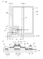
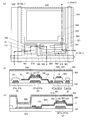
- FIG. 3A is an enlarged plan view showing the configuration of the pixel 20 formed on the active matrix substrate 100
- FIG. 3B shows the pixel 20 along the line BB shown in FIG. FIG.
- the pixel 20 includes a TFT 110 (first thin film transistor) that functions as a switching element, a pixel electrode 123, and a storage capacitor forming unit 50.
- the pixel 20 transmits backlight light corresponding to an image signal by changing the transmittance of the backlight light with a liquid crystal material.
- the pixel 20 is provided near the intersection of the i-th scanning signal line 21 (GLi) and the j-th data signal line 61 (SLj).
- the j-th storage capacitor line 51 (CSLj) is disposed so as to run vertically near the center of the pixel 20.
- the TFT 110 includes a gate electrode 121, a gate insulating layer 131, a semiconductor layer 141, a channel protective layer 151 (first protective layer), a source electrode 161, and a drain electrode 162.
- the gate electrode 121 is branched from the scanning signal line 21 (GLi), and the source electrode 161 is branched from the data signal line 61 (SLj).
- the upper surface of the semiconductor layer 141 is covered with a channel protective layer 151.
- the source electrode 161 is electrically connected to the left upper surface and side surfaces of the semiconductor layer 141
- the drain electrode 162 is electrically connected to the right upper surface and side surfaces of the semiconductor layer 141.
- the drain electrode 162 is connected to the pixel electrode 123 via the drain lead line 163. Openings 185a and 185b are provided in the gate insulating layer 131 on both sides of the storage capacitor forming portion 50 so that the surface of the pixel electrode 123 is exposed.
- the storage capacitor forming unit 50 includes a storage capacitor line 51 (CSLj) disposed so as to face the gate insulating layer 131 and a portion of the electrode 124 that faces the storage capacitor line 51. It has a function of stabilizing the potential of the pixel electrode 123 that is electrically connected.
- CSLj storage capacitor line 51
- the scanning signal line 21 and the gate electrode 121 have a two-layer structure including upper layers 21b and 121b and lower layers 21a and 121a, respectively.
- the lower layers 21a and 121a are formed of the same transparent metal film as the pixel electrode 123, and the upper layers 21b and 121b are formed of the same metal film as the electrode 124.
- the data signal line 61, the source electrode 161, the drain electrode 162, the drain lead line 163, and the storage capacitor line 51 are made of the same metal film.
- a protective layer 171 (second protective layer) made of an insulating film is formed on the upper surface thereof.
- a channel protective layer 151 made of an insulating film is formed on the upper surface of the semiconductor layer 141.
- a TFT in which the source electrode 161 and the drain electrode 162 are formed so as to cover part of the upper surface of the semiconductor layer 141 like the TFT 110 may be referred to as a top contact type TFT.
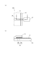
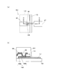
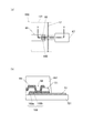
- FIG. 4A is a plan view showing the configuration of the gate terminal 25A
- FIG. 4B is a cross-sectional view of the gate terminal 25A along the line CC shown in FIG. 4A.
- the gate terminal electrode 27 is electrically connected to the scanning signal line 21 via the gate lead line 26.
- the gate lead line 26 has a two-layer structure including a lower layer 26a and an upper layer 26b.
- the lower layer 26a and the upper layer 26b are made of the same metal film as the lower layer 121a and the upper layer 121b of the gate electrode 121, respectively.
- the gate terminal electrode 27 has a single layer structure and is made of the same transparent metal film as the lower layer 121 a of the gate electrode 121.
- the gate lead line 26 is covered with the gate insulating layer 131, but the gate terminal electrode 27 is not covered.
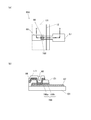
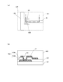
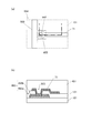
- FIG. 5A is a plan view showing the configuration of the source terminal 65A
- FIG. 5B is a cross-sectional view of the source terminal 65A along the line DD shown in FIG. 5A.
- the source terminal electrode 67 is electrically connected to the source lead line 66 through the connection layer 168 that forms the contact hole 68.
- the source lead line 66 is connected to the data signal line 61.
- the source lead line 66 is made of the same metal film as the source electrode 161.
- the connection layer 168 has a two-layer structure including an upper layer 168b and a lower layer 168a, and is formed of the same metal film as the upper layer 121b and the lower layer 121a of the gate electrode 121, respectively.
- the source terminal electrode 67 has a single layer structure and is made of the same transparent metal film as the lower layer 121 a of the gate electrode 121.
- the source lead line 66 and the connection layer 168 are covered with the gate insulating layer 131 except for the contact hole 68, but the source terminal electrode 67 is not covered.
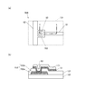
- FIG. 6A is a plan view showing the configuration of the contact portion 54A
- FIG. 6B is a cross-sectional view of the contact portion 54A along the line EE shown in FIG. 6A.
- the storage capacitor wiring 51 is electrically connected to the storage capacitor wiring trunk 52 through a connection layer 153 that forms a contact hole 53 provided in the gate insulating layer 131.
- the storage capacitor wiring trunk 52 has a two-layer structure including an upper layer 52b and a lower layer 52a, and is formed of the same metal film as the upper layer 121b and the lower layer 121a of the gate electrode 121, respectively.
- the storage capacitor wiring terminal 55A replaces the gate lead line 26 with the storage capacitor line trunk lead line 56 in the gate terminal 25A shown in FIGS. 4A and 4B, and replaces the gate terminal electrode 27 with the storage capacitor terminal. Since only the electrode needs to be replaced, a diagram illustrating the configuration of the storage capacitor wiring terminal 55A and the description thereof are omitted.
- the semiconductor layer 141 serving as the channel of the TFT 110 formed on the active matrix substrate 100 is made of an oxide semiconductor film such as indium, gallium, zinc oxide (IGZO), for example.
- the scanning signal line 21 and the gate electrode 121 include, for example, an indium / tin oxide (ITO) film formed on the glass substrate 101, a titanium (Ti) film, an aluminum (Al) film on the surface of the ITO film, It consists of Ti / Al / Ti laminated film laminated
- the data signal line 61, the source electrode 161, the drain electrode 162, and the storage capacitor wiring 51 are made of, for example, an Al / Ti laminated film in which a Ti film and an Al film are laminated in this order from the glass substrate 101 side.
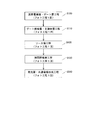
- FIG. 7 is a flowchart showing a manufacturing process of the active matrix substrate 100.
- the manufacturing process of the active matrix substrate 100 includes three processes of a pixel electrode layer / gate layer process S100, a gate insulating layer / semiconductor layer process S110, and a source layer process S120. As will be described later, since each process includes a photolithography process once, a total of three photomasks are used to manufacture the active matrix substrate 100.
- FIG. 8 is a flowchart showing detailed manufacturing steps of the gate insulating layer / semiconductor layer step S110 in the manufacturing steps of the active matrix substrate 100 shown in FIG.
- FIG. 9 to 14 are process cross-sectional views showing the manufacturing process of the active matrix substrate 100.
- FIG. Each of FIG. 9 to FIG. 14A is a process sectional view of the pixel 20 along the line BB shown in FIG. 3A, and each of FIG. 9 to FIG. 14B corresponds to FIG.
- FIG. 15C is a process cross-sectional view of the gate terminal 25A along the line CC shown in FIG. 9, and each of FIGS. FIG. 9D to FIG. 14D are process cross-sectional views of the contact portion 54A along the line EE shown in FIG. 6A.
- an ITO film (not shown) that becomes the lower layer 121a of the gate electrode 121 is formed on the glass substrate 101 by a sputtering method using argon (Ar) gas, and then Ti / B that becomes the upper layer 121b of the gate electrode 121 is formed.
- An Al / Ti laminated film (not shown) is continuously formed.
- the thickness of the ITO film is, for example, 100 nm.
- the film thickness of each of the Ti / Al / Ti laminated films is 30 nm, 200 nm, and 150 nm in order from the glass substrate 101 side.
- the temperature of the glass substrate 101 at the time of forming these films is set to 100 to 200 ° C., for example.
- the ITO film and the Ti / Al / Ti laminated film may be collectively referred to as a gate metal film.
- each of the scanning signal line 21, the gate electrode 121, and the processed layers 41 to 44 has a two-layer structure, and each of the lower layers 21a, 121a, 41a to 44a is made of an ITO film, and the upper layers 21b, 121b, 41b. ⁇ 44b is made of a Ti / Al / Ti laminated film.
- the processed layer 41 may be referred to as a first processed layer
- the processed layer 42 may be referred to as a second processed layer
- the processed layer 43 may be referred to as a third processed layer.
- etching the Ti / Al / Ti laminated film for example, a dry etching method in which gases such as chlorine (Cl 2) gas, boron trichloride (BCl 3) gas, and argon gas are appropriately combined is used.
- gases such as chlorine (Cl 2) gas, boron trichloride (BCl 3) gas, and argon gas are appropriately combined
- a wet etching method using an aqueous ferric chloride (FeCl 3 ) solution or an oxalic acid (HOOC-COOH) solution is used.
- the temperature of the etchant used for etching the ITO film is set to 20 to 40 ° C., for example.
- the Ti / Al / Ti laminated film may be etched using an etchant containing hydrofluoric acid (HF) and nitric acid (HNO 3 ), and the Ti / Al / Ti laminated film is used using the same etchant.
- the ITO film may be continuously etched. The process up to here may be referred to as a first process.
- the gate insulating layer / semiconductor layer step S110 includes a film formation / resist pattern formation step S111, a first etching step S112, an ashing / second etching step S113, and a peeling step S114.
- a silicon nitride (SiNx) film (not shown) and a silicon oxide (SiOx) film (not shown) are successively formed by plasma CVD (Chemical Vapor Deposition).
- Silane (SiH 4), ammonia (NH 3), hydrogen (H 2), nitrogen (N 2) gas, or the like is used for the formation of the silicon nitride film, and silane and dinitrogen monoxide ( N2O) gas or the like is used.
- an insulating film 136 (first insulating film) made of a SiOx / SiNx laminated film is formed.
- An amorphous oxide semiconductor film 146 is formed over the insulating film 136 by a sputtering method using an argon gas.
- the thickness of the oxide semiconductor film 146 is, for example, 50 nm.
- a sintered body of a mixture of indium oxide (In2O3), gallium oxide (Ga2O3), and zinc oxide (ZnO) is used as a sputtering target.
- the composition ratio (atomic ratio) of indium, gallium, and zinc contained in the IGZO film is adjusted so as to be the same ratio as shown in the following formula (1).
- Indium: gallium: zinc 1: 1: 1 (1)
- the temperature of the glass substrate 101 during the formation of the IGZO film is set to 100 to 200 ° C., for example.
- the film thickness and composition ratio of the IGZO film are not limited to the range shown in Formula (1), and the composition ratios (atom ratio) of indium, gallium, and zinc may be different from each other.
- An insulating film 156 (second insulating film) made of a silicon oxide film is formed over the oxide semiconductor film 146 by a plasma CVD method using a gas such as silane and dinitrogen monoxide.
- the film thickness of the insulating film 156 is, for example, 150 nm.
- the temperature of the glass substrate 101 when forming the insulating film 156 is set to 200 to 300 ° C., for example. The process up to here may be referred to as a second process.
- a resist pattern 181 is formed on the insulating film 156 by using a photolithography method.
- the resist pattern 181 is formed by exposing a resist film using a gray tone mask or a half tone mask in which a transmission pattern, a semi-transmission pattern, and a non-transmission pattern are formed on a single quartz substrate.
- a thick resist pattern 181a (second resist pattern) formed by blocking exposure light on the insulating film 156 by the non-transmissive pattern and a thin resist formed by exposure light transmitted through the semi-transmissive pattern.
- a resist pattern 181 including the pattern 181b (first resist pattern) is formed.
- the resist pattern 181 including the thick resist pattern 181a and the thin resist pattern 181b can be formed by one photolithography process. Manufacturing cost can be reduced.
- the thick resist pattern 181a is formed in a region where a channel protection layer 151 of the TFT 110 described later is to be formed.
- the thin resist pattern 181b is a region where a gate insulating layer 131 described later is to be left, such as a region where a portion protruding from the channel protective layer 151 in a semiconductor layer 141 described later is to be formed, a region where a storage capacitor forming portion 50 is to be formed, and the like. Formed.
- the first etching step S112 will be described with reference to FIGS. 11 (a) to 11 (d).
- the insulating film 156, the oxide semiconductor film 146, and the insulating film 136 are sequentially etched using the thick resist pattern 181a and the thin resist pattern 181b as a mask.
- a dry etching method in which gases such as carbon tetrachloride (CF 4) gas and oxygen (O 2) gas are appropriately combined is used.
- a wet etching method using an etchant containing oxalic acid or an etchant containing phosphoric acid, acetic acid, nitric acid, or the like is used.
- the oxide semiconductor film 146 may be etched by a dry etching method in which gases such as carbon tetrachloride gas, oxygen gas, and argon gas are appropriately combined instead of the wet etching method.
- the gate insulating layer 131 is formed from the insulating film 136 and the surface of the pixel electrode 123 is exposed.
- the gate lead line 26 is formed from the lower layer 42a and the upper layer 42b of the processed layer 42
- the gate terminal electrode 27 is formed from the lower layer 42a.
- a contact hole 68 reaching the surface of the lower layer 43a of the processed layer 43 is opened.
- a lower layer 168a and an upper layer 168b constituting the connection layer 168 are formed from the lower layer 43a and the upper layer 43b, respectively, and a source terminal electrode 67 is formed from the lower layer 43a.
- a contact hole 53 reaching the surface of the lower layer 153a of the connection layer 153 connected to the storage capacitor wiring trunk 52 is opened, and the lower layer constituting the connection layer 153 from the lower layer 44a and the upper layer 44b of the processed layer 44 153a and upper layer 153b are formed.
- the ashing / second etching step S113 will be described with reference to FIGS. 12 (a) to 12 (d).
- the resist pattern 181 is half-ashed to remove the thin resist pattern 181b and leave the thick resist pattern 181a.
- Half ashing is performed using a combination of carbon tetrachloride gas and oxygen gas.
- the insulating film 156 and the oxide semiconductor film 146 are etched by a dry etching method using the remaining thick resist pattern 181a as a mask. Thereby, the channel protective layer 151 and the semiconductor layer 141 are formed.
- the insulating film 156 and the oxide semiconductor film 146 are removed, and the surface of the gate insulating layer 131 is exposed.
- the thick resist pattern 181a is stripped using a stripping solution containing organic alkali.
- the process up to here may be referred to as a third process.
- the source layer step S120 will be described with reference to FIGS. 14 (a) to 14 (d).
- a source metal film 166 made of a Ti / Al laminated film is formed so as to cover the entire glass substrate 101 by a sputtering method using argon gas.
- the film thickness of the titanium film constituting the source metal film 166 is 200 nm, and the film thickness of the aluminum film is 30 nm.
- the temperature of the glass substrate 101 during the formation of the source metal film 166 is set to 100 to 200 ° C., for example.
- a protective film 176 is formed on the source metal film 166 by plasma CVD.
- a resist pattern 183 (third resist pattern) is formed over the protective film 176 by photolithography.
- the data signal line 61, the source electrode 161, the drain electrode 162, the drain lead line 163, and the storage capacitor line 51 are to be formed, and the source lead line 66 of the source terminal 65A is to be formed. Formed on the region.
- the protective film 176 and the source metal film 166 are etched in this order. Thereby, as shown in FIG. 3B, a protective layer 171 is formed from the protective film 176, and the data signal line 61, the source electrode 161, the drain electrode 162, the drain lead line 163, and the storage capacitor line are formed from the source metal film 166. 51, source lead lines 66, and storage capacitor lines 51 are formed. Further, the surfaces of the pixel electrode 123, the gate terminal electrode 27, and the source terminal electrode 67 are exposed.
- a dry etching method in which gases such as carbon tetrafluoride gas and oxygen gas are appropriately combined is used.
- etching of the source metal film 166 for example, a dry etching method in which gases such as chlorine gas, boron trichloride gas, and argon gas are appropriately combined is used. Further, the resist pattern 183 is stripped using a stripping solution containing an organic alkali. The process up to here may be referred to as a fourth process. In this way, the active matrix substrate 100 shown in FIGS. 3 to 6 is manufactured.
- FIGS. 15A to 15E are process cross-sectional views showing changes in shape when the channel protective layer 151 and the semiconductor layer 141 shown in FIG. 12 are formed by a dry etching method.
- a thin resist pattern (not shown) is removed by half ashing.
- the remaining thick resist pattern 181a is reduced in thickness by half ashing.
- the insulating film 156 and the oxide semiconductor film 146 are etched in this order by a dry etching method using the thick resist pattern 181a as a mask to form a channel protective layer 151 and a semiconductor layer 141.
- the thick resist pattern 181 a becomes a resist pattern 182 with a reduced thickness and a reduced shape, and the surface of the channel protective layer 151 is exposed around the resist pattern 182.
- the channel protective layer 151 is further etched using the resist pattern 182 as a mask. As a result, the channel protective layer 151 becomes the channel protective layer 152 having the same size as the reduced resist pattern 182. As a result, the peripheral portion of the semiconductor layer 141 protrudes from the edge of the channel protective layer 152, so that a step is formed between the semiconductor layer 141 and the channel protective layer 152, and they are stacked stepwise.
- the resist pattern 182 is removed. Then, a source electrode 161 extending from the left upper surface of the channel protective layer 152 to the left side and a drain electrode 162 extending from the right upper surface of the channel protective layer 152 to the right side are formed.
- the source electrode 161 is electrically connected to the left side surface and the upper left surface of the semiconductor layer 141
- the drain electrode 162 is electrically connected to the right side surface and the upper right surface of the semiconductor layer 141. Connected. Accordingly, the reliability of electrical connection between the source electrode 161 and the drain electrode 162 and the semiconductor layer 141 can be increased.
- the manufacturing cost of the active matrix substrate 100 can be reduced.
- the etching rates of the thick resist pattern 181a, the insulating film 156, and the oxide semiconductor film 146 are substantially the same.
- FIG. 15B if the etching is performed in such a condition that the etching rate is reduced in the order of the thick resist pattern 181a, the insulating film 156, and the oxide semiconductor film 146, FIG.
- the step (d) can be omitted.
- the step between the semiconductor layer 141 and the channel protective layer 151 can be more simply formed, so that the manufacturing cost of the active matrix substrate 100 can be further reduced.
- the channel protective layer becomes smaller than the semiconductor layer, so that the source electrode and the drain electrode are not only the side surfaces of the semiconductor layer but also the upper surface thereof. Electrically connected.
- the channel protective layer is described as having the same size as the semiconductor layer.
- etching is performed using the thick resist pattern 181a and the thin resist pattern 181b as a mask, and the gate terminal electrode 27, the source terminal electrode 67, the pixel electrode 123, and the contact hole of the storage capacitor wiring trunk 52 are formed. 53 is formed.
- etching is performed using the remaining thick resist pattern 181a as a mask to form the semiconductor layer 141 of the TFT 110 and the channel protective layer 151 on the upper surface of the semiconductor layer 141.
- etching is performed using the resist pattern 183 as a mask, which is held by the source electrode 161, the drain electrode 162, the drain lead line 163, the source lead line 66, the data signal line 61, and the contact hole 53.
- a storage capacitor line 51 connected to the capacitor line trunk 52 is formed. In this manner, necessary components including the pixel electrode 123 can be formed even if the resist pattern is formed once in each step. As a result, the number of photolithography processes that require a large number of manufacturing facilities in the manufacturing process can be reduced, and the manufacturing cost of the active matrix substrate 100 can be reduced.
- FIG. 16A is an enlarged plan view showing the configuration of the pixel 20 formed on the active matrix substrate 200, and FIG. 16B shows the pixel 20 along the line FF shown in FIG.
- FIG. 17A is a plan view showing a configuration of a gate terminal 25B which is a modified example of the gate terminal 25A shown in FIG. 4, and FIG. 17B is along the line GG shown in FIG. It is sectional drawing of the gate terminal 25B.
- FIG. 18A is a plan view showing a configuration of a source terminal 65B which is a modification of the source terminal 65A shown in FIG. 5, and FIG. 18B is along the line HH shown in FIG.
- FIG. 19A is a plan view showing a configuration of a contact portion 54B (first contact portion) which is a modification of the contact portion 54A shown in FIG. 6, and FIG. 19B is a plan view of FIG. 19A. It is sectional drawing of the contact part 54B along the II line shown.
- the protective layer 171 is not provided on the surface of the source electrode 161, the drain electrode 162, and the like. Therefore, the configuration of the active matrix substrate 200 in which the protective layer 171 is not provided will be described.
- the same components as those shown in FIGS. 3 to 6 are designated by the same reference numerals and description thereof is omitted.
- the protective layer 171 is not provided on the surface of the active matrix substrate 200, the data signal line 61, the drain lead line 163, the storage capacitor line 51, the source lead line 66, and the source electrode 161 of the TFT 210 (first thin film transistor) The surface of the drain electrode 162 is exposed. Therefore, in order to ensure the corrosion resistance of these wirings, it is preferable to arrange a titanium layer having a relatively high corrosion resistance or a metal layer mainly composed of titanium in the uppermost layer of these wirings. Specifically, these wirings are preferably formed using any one of a Ti / Al / Ti laminated film, a Ti / Al laminated film, a Ti / Cu / Ti laminated film, and a Ti / Al laminated film. Thereby, the reliability of the active matrix substrate 200 can be increased. In addition, since it is not necessary to form the protective layer 171 for preventing corrosion, the manufacturing cost of the active matrix substrate 200 can be reduced.
- FIG. 20A is a plan view showing a configuration of a gate terminal 25C, which is a modification of the gate terminal 25A shown in FIG. 4, and FIG. 20B shows a line JJ shown in FIG. 20A. It is sectional drawing of the gate terminal 25C along.
- FIG. 21A is a plan view showing a configuration of a source terminal 65C, which is a modification of the source terminal 65A shown in FIG. 5, and FIG. 21B is a cross-sectional view taken along line KK shown in FIG. It is sectional drawing of the source terminal 65C along.
- the gate terminal electrode 27 is formed only of a transparent metal film such as ITO, the electric resistance tends to be high. For this reason, when the active matrix substrate 100 shown in FIG. 3 is used for a large display device such as a liquid crystal television, the display quality may be lowered. Therefore, in the gate terminal 25C, the periphery of the gate terminal electrode 27 made of a transparent metal film is surrounded by the conductive layer 28 (first conductive layer). Since the conductive layer 28 is made of a Ti / Al / Ti film like the upper layer 121b of the gate electrode 121, the conductivity is high. By providing such a conductive layer 28, the electrical resistance of the gate terminal 25C can be reduced auxiliary.
- the gate terminal 25C the waveform deterioration of the electric signal input from the external substrate 9 through the anisotropic conductive film (ACF) or the like is suppressed. If an active matrix substrate having such a gate terminal 25C is used in a large display device such as a liquid crystal television, the display quality can be prevented from deteriorating.
- ACF anisotropic conductive film
- the source terminal 65 ⁇ / b> C surrounds the source terminal electrode 67 made of only ITO with a conductive layer 69.
- the conductive layer 69 (first conductive layer) is made of a Ti / Al / Ti film like the conductive layer 28, the conductivity is high. Thereby, similarly to the case of the gate terminal 25C, the waveform deterioration of the electric signal inputted from the external substrate 9 inputted through the ACF or the like can be suppressed also at the source terminal 65C, and display quality can be obtained if it is used for a large display device. Can be prevented.
- the conductive layer 28 formed around the gate terminal electrode 27 and the conductive layer 69 formed around the source terminal electrode 67 are covered with a gate insulating layer 131. For this reason, the reliability of the conductive layer 28 and the conductive layer 69 is ensured.
- FIG. 22A is a diagram showing a path through which a current flows through the gate terminal 25A in which the conductive layer 28 is not formed around the gate terminal electrode 27.
- FIG. 22B is a diagram around the gate terminal electrode 27. It is a figure which shows the path
- connection point P between the conductive particles contained in the ACF and the gate terminal electrode 27 is used.
- the current supplied from the external substrate 9 flows in the direction of the arrow toward the gate lead line 26.
- the gate terminal electrode 27 consists only of a transparent metal film, its resistance value is very high. For this reason, the waveform of an electric signal deteriorates.
- a conductive layer 28 is formed around the gate terminal electrode 27.
- the position of the connection point P between the conductive particles contained in the ACF and the gate terminal electrode 27 is assumed to be the same as that shown in FIG.
- the path having the lowest resistance value is a path indicated by an arrow line. That is, this is a path connecting the connection point P and the position Q of the conductive layer 28 closest to the connection point P by a straight line, and further from the position Q to the gate lead line 26 along the conductive layer 28. Therefore, if the current supplied from the external substrate 9 flows through such a path having the lowest resistance value, the waveform deterioration of the electric signal can be prevented.
- the conductivity of the conductive layer 28 is 1/10 to 1/100 of the conductivity of the transparent metal film, a path away from the gate lead line 26 such as a path from the position P to the position Q is included. Even in this case, the substantial resistance value is almost the same. Further, although the gate terminal 25C has been described here, the same applies to the source terminal 65C.
- FIG. 23 is a diagram illustrating a gate terminal 25D which is another modification of the gate terminal 25A.
- the gate terminal 25D not only the conductive layer 28 is formed around the gate terminal electrode 27, but also a lattice-like conductive material electrically connected to the surrounding conductive layer 28 inside thereof.
- Layer 29 (second conductive layer) is formed.
- the gate terminal 25D has been described as an example, but the same applies to the source terminal.
- the configuration of the active matrix substrate 300 included in the liquid crystal display device according to the present embodiment is substantially the same as that of the active matrix substrate 100 shown in FIG.
- FIG. 24A is an enlarged plan view showing the configuration of the pixel 20 formed on the active matrix substrate 300
- FIG. 24B shows the pixel 20 along the line LL shown in FIG. FIG.
- the components of the active matrix substrate 300 shown in FIG. 24A the same components as those of the active matrix substrate 100 shown in FIG. Explained.
- the semiconductor layer 341 of the TFT 310 (first thin film transistor) is formed on the gate insulating layer 131 sandwiched between the source electrode 361 and the drain electrode 362.
- the lower surface is electrically connected to the upper surfaces of the source electrode 361 and the drain electrode 362.
- the upper surface of the semiconductor layer 341 is covered with a protective layer 351 (third protective layer).
- a TFT in which the semiconductor layer 341 is provided on the top surfaces of the source electrode 361 and the drain electrode 362 like the TFT 310 may be referred to as a bottom contact type TFT.
- the pixel electrode 123 is directly connected to the drain lead line 163.
- the pixel electrode 323 is electrically connected to the drain lead line 363 via the connection electrode 343 (first connection electrode) made of the same layer as the semiconductor layer 341.
- the connection electrode 343 is covered with a protective layer 351.
- FIG. 25A is a plan view showing a configuration of a gate terminal 25E which is a modification of the gate terminal 25A shown in FIG. 4, and FIG. 25B is a cross-sectional view taken along line MM shown in FIG. It is sectional drawing of the gate terminal 25E along.
- the gate terminal 25E has the same configuration as the gate terminal 25A shown in FIGS. 4 (a) and 4 (b). The description is omitted.
- FIG. 26A is a plan view showing a configuration of a source terminal 65E which is a modification of the source terminal 65A shown in FIG. 5, and FIG. 26B shows a line NN shown in FIG. It is sectional drawing of the source terminal 65E along.
- the source terminal electrode 67 is electrically connected to the source lead line 66 through the connection layer 168 having the contact hole 68.
- the source lead line 66 is electrically connected to the connection electrode 344 (second connection electrode) and connected.
- the electrode 344 is electrically connected to the connection layer 168.
- the source lead line 66 is electrically connected to the source terminal electrode 67.
- the source lead line 66 is formed in the same process as the source electrode 361 and is made of a source metal film.
- the connection electrode 344 is formed in the same step as the semiconductor layer 341 and is formed using an oxide semiconductor film. Further, the connection electrode 344 is covered with the protective layer 351, but the source terminal electrode 67 is not covered.
- FIG. 27A is a plan view showing a configuration of a contact portion 54E which is a modification of the contact portion 54A shown in FIG. 6, and FIG. 27B is a cross-sectional view taken along the line PP shown in FIG. It is sectional drawing of the contact part 54E along.
- the storage capacitor line 51 is electrically connected to the storage capacitor line trunk 52 through the connection layer 153 having the contact hole 53.
- the storage capacitor wiring 51 is electrically connected to the connection electrode 345 and connected.
- the electrode 345 is electrically connected to the connection layer 153.
- the storage capacitor line 51 is electrically connected to the storage capacitor line trunk 52.
- the storage capacitor line 51 is formed in the same process as the source electrode 361 and is made of a source metal film.
- the connection electrode 345 is formed in the same process as the semiconductor layer 341 and is formed using an oxide semiconductor film.
- the connection electrode 345 is covered with a protective layer 351.
- the storage capacitor wiring terminal replaces the gate lead line 26 of the gate terminal 25E shown in FIGS. 25A and 25B with a storage capacitor wiring main lead line 56, and replaces the gate terminal electrode 27 with the storage capacitor wiring terminal electrode. Therefore, the illustration of the configuration of the storage capacitor wiring terminal and the description thereof are omitted.
- FIG. 28 is a flowchart showing manufacturing steps of the active matrix substrate 300
- FIG. 29 is a flowchart showing detailed manufacturing steps of the gate insulating layer / source layer step S310 in the manufacturing steps shown in FIG.
- the manufacturing process of the active matrix substrate 300 includes three processes of a pixel electrode layer / gate layer process S100, a gate insulating layer / source layer process S310, and a semiconductor layer process S320.
- each process includes a photolithography process once, so that a total of three photomasks are used to manufacture the active matrix substrate 300.
- a gate insulating layer / source layer step S310 is provided instead of the gate insulating layer / semiconductor layer step S110 shown in FIG. 7, and a semiconductor layer step S320 is provided instead of the source layer step S120. . Therefore, in the following description, the pixel electrode layer / gate layer step S100 will be briefly described, and the gate insulating layer / source layer step S310 and the semiconductor layer step S320 will be described.
- FIGS. 30 to 34 are process cross-sectional views showing the manufacturing process of the active matrix substrate 300.
- FIG. Each of FIGS. 30 to 34 is a process sectional view of the pixel 20 along the line LL shown in FIG. 24A, and each of FIGS. 30 to 34 is shown in FIG.
- FIG. 30C is a process cross-sectional view of the gate terminal 25E along the line MM shown in FIG. 30, and each of FIGS. 30 to 34C is a process cross-section of the source terminal 65E along the line NN shown in FIG.
- FIGS. 30 to 34D are process sectional views of the contact portion 54E along the line PP shown in FIG. 27A.
- the scanning signal line 21, the gate electrode 121, and the processed layers 41 to 44 are formed on the glass substrate 101 in the same manner as in the first embodiment.
- each of the scanning signal line 21, the gate electrode 121, and the processed layers 41 to 44 has a two-layer structure, and each of the lower layers 21a, 121a, 41a to 44a is made of an ITO film, and the upper layers 21b, 121b, 41b to 44b are made of a Ti / Al / Ti laminated film.
- the process up to here may be referred to as a first process.
- a silicon nitride film and a silicon oxide film are successively formed so as to cover the scanning signal line 21, the gate electrode 121, and the like, and an insulating film 136 is formed.
- the source gas, the film thickness, and the temperature of the glass substrate 101 at the time of forming the silicon nitride film and the silicon oxide film are the same as those in the first embodiment, and thus description thereof is omitted.
- the gate insulating layer / source layer step S310 includes a film forming / resist pattern film forming step S311, a first etching step S312, an ashing / second etching step S313, and a peeling step S314.
- a source metal film 366 is formed on the insulating film 136 as shown in FIGS. 30 (a) to 30 (d).
- the source metal film 366 is made of an Al / Ti laminated film. Note that the method for forming the source metal film 366, the film thickness, and the temperature of the glass substrate 101 are the same as those in the first embodiment, and a description thereof will be omitted. The process up to here may be referred to as a second process.
- a resist pattern 381 is formed on the source metal film 366 using photolithography.
- the resist pattern 381 is formed by exposing using a gray-tone mask or a half-tone mask.
- a resist pattern 381 including a thick resist pattern 381a (second resist pattern) and a thin resist pattern 381b (first resist pattern) is formed on the source metal film 366.
- the resist pattern 381 including the thick resist pattern 381a and the thin resist pattern 381b can be formed in one photolithography process. Manufacturing cost can be reduced.
- the thick resist pattern 381a is formed in a region where a source electrode 361, a drain electrode 362, a drain lead line 363, a data signal line 61, a storage capacitor line 51, and a source lead line 66 of the TFT 310 to be described later are to be formed.
- the thin resist pattern 381b includes a gate insulating layer described later such as a region to be sandwiched between the source electrode 361 and the drain electrode 362 of the TFT 310, a region above the scanning signal line 21, and a region adjacent to the region where the storage capacitor wiring 51 is to be formed. 131 is formed in the region to be left.
- the source metal film 366, the insulating film 136, The upper layers 41b, 42b, 43b and 44b of the processed layers 41 to 44 are etched in order.
- a dry etching method in which gases such as carbon tetrachloride gas and oxygen gas are appropriately combined is used.
- etching the source metal film 366 and the upper layers 41b, 42b, 43b, and 44b of the processed layers 41 to 44 for example, a dry etching method in which gases such as chlorine gas, boron trichloride gas, and argon gas are appropriately combined is used. .
- gases such as chlorine gas, boron trichloride gas, and argon gas are appropriately combined.
- the pixel electrode 123 is formed from the lower layer 41a of the processed layer 41, and the electrode 124 is formed from the upper layer 41b. Further, the gate lead line 26, the connection layer 168, and the lower layers 26a, 168a, and 153a of the connection layer 153 are formed from the lower layers 42a to 44a of the processed layers 42 to 44, respectively, and the gate lead line 26 and the connection layer 168 are formed from the upper layers 42b to 44b. The upper layers 26b, 168b, 153b of the connection layer 153 are formed.
- the resist pattern 381 is half-ashed to remove the thin resist pattern 381b, and the thick resist pattern 381a is removed. leave.
- the remaining thick resist pattern 381a is reduced in thickness by half ashing.
- the source metal layer 367 is etched by dry etching using the remaining thick resist pattern 381a as a mask. Thereby, the data signal line 61, the source electrode 361, the drain electrode 362, the drain lead line 363, the storage capacitor line 51, and the source lead line 66 are formed.
- the half ashing of the resist pattern 381 is the same as that in the first embodiment, and the description thereof is omitted.
- the source metal layer 367 is etched by using a dry etching method in which gases such as chlorine gas, boron trichloride gas, and argon gas are appropriately combined, similarly to the etching of the source metal film 366 in the first etching step S312. Do it.
- the thick resist pattern 381a is stripped using a stripping solution containing an organic alkali.
- the process up to here may be referred to as a third process.
- an oxide semiconductor film 346 made of an IGZO film is formed on the gate insulating layer 131 as shown in FIGS.
- the oxide semiconductor film 346 is formed by sputtering as in the case of the first embodiment. Since the deposition method and composition ratio of the oxide semiconductor film 346 are the same as those in the first embodiment, description thereof is omitted. Further, since the thickness of the oxide semiconductor film 346 and the temperature of the glass substrate 101 at the time of film formation are the same as those in the first embodiment, description thereof is omitted.
- a protective film 356 (second insulating film) made of a silicon oxide film is formed over the oxide semiconductor film 346 by a plasma CVD method using a gas such as silane and dinitrogen monoxide.
- the thickness of the protective film 356 is, for example, 150 nm.
- the temperature of the glass substrate 101 when forming the protective film 356 is set to 200 to 300 ° C., for example.
- a resist pattern 383 (third resist pattern) is formed on the protective film 356 by using a photolithography method.
- the protective film 356 and the oxide semiconductor film 346 are etched in this order using the resist pattern 383 as a mask. Thereby, as shown in FIGS. 24B, 26B, and 27B, the protective layer 351, the semiconductor layer 341, and the connection electrodes 343 to 345 are formed. Note that the etching of the protective film 356 and the oxide semiconductor film 346 is the same as that in the first embodiment, and a description thereof will be omitted.
- the resist pattern 383 is stripped using a stripping solution containing an organic alkali.
- the process up to here may be referred to as a fourth process. In this way, the active matrix substrate 300 shown in FIGS. 24 to 27 is manufactured.
- the IGZO film is susceptible to substrate heat treatment.
- the characteristics of the TFT 310 may be affected by the temperature (for example, 100 ° C. to 200 ° C.) applied to the active matrix substrate 300.
- the IGZO film is not affected by the temperature at which the source metal film 366 is formed. Therefore, the characteristics of the TFT 310 are more stable than those of the top contact type TFT 110.
- Such a TFT 310 further has the following effects.
- etching is performed using the thick resist pattern 381a and the thin resist pattern 381b as masks, and the contact holes of the gate terminal electrode 27, the source terminal electrode 67, the pixel electrode 123, and the storage capacitor wiring trunk 52 are formed. 53 is formed.
- the remaining thick resist pattern 381a is etched as a mask, and the source electrode 161, the drain electrode 162, the drain lead line 163, the source lead line 66, and the data signal line are etched. 61 and the storage capacitor wiring 51 connected to the storage capacitor wiring trunk 52 through the contact hole 53 are formed.
- the protective film 356 and the oxide semiconductor film 346 are sequentially etched using the resist pattern 383 as a mask to form the semiconductor layer 341, the connection electrodes 343 to 345, and the protective layer 351 covering them. .
- necessary components including the pixel electrode 123 can be formed even if the resist pattern is formed once in each step.
- the number of photolithography processes requiring a large number of manufacturing facilities in the manufacturing process can be reduced, and the manufacturing cost of the active matrix substrate 300 can be reduced.
- the drain lead line 363 and the pixel electrode 123, the source lead line 66 and the source terminal electrode 67 of the source terminal 65E, and the storage capacitor line 51 and the storage capacitor line trunk 52 cannot be directly connected. Therefore, the oxide semiconductor film 346 is etched using the third resist pattern 383 as a mask, so that the connection electrode 343 connecting the drain lead line 363 and the pixel electrode 123, and the source lead line 66 and the source terminal electrode 67 are connected. And the connection electrode 345 for connecting the storage capacitor wiring 51 and the storage capacitor wiring trunk 52 are formed.
- the drain lead line 363 and the pixel electrode 123, the source lead line 66 and the source terminal electrode 67, and the storage capacitor line 51 and the storage capacitor line trunk 52 are connected without adding a new manufacturing process. Therefore, the manufacturing cost of the active matrix substrate 300 can be reduced.
- the configuration of the active matrix substrate 400 included in the liquid crystal display device according to the present embodiment is substantially the same as the configuration of the active matrix substrate 100 shown in FIG.
- FIG. 35A is an enlarged plan view showing the configuration of the pixel 20 formed on the active matrix substrate 400
- FIG. 35B shows the pixel 20 along the line QQ shown in FIG. FIG.
- the configuration of the TFT 410 first thin film transistor
- the data signal line 61 the data signal line 61
- the scanning signal line 21 the storage capacitor forming portion 50
- the pixel electrode 123 is the first. This is the same as the case of the embodiment. Therefore, among the components of the active matrix substrate 400, the same components as those of the active matrix substrate 100 shown in FIGS. 3A and 3B are denoted by the same reference numerals, and different components are designated. The explanation is centered.
- the active matrix substrate 400 is different from the active matrix substrate 100 in that the protective layer 171 is not formed on the upper surfaces of the source electrode 161, the drain electrode 162, and the like, and instead, an interlayer is formed so as to cover the surface of the active matrix substrate 400.
- An insulating layer 491 is formed. Note that openings 186a and 186 of the interlayer insulating layer 491 are provided over the pixel electrodes 123 inside the openings 185a and 185b provided in the gate insulating layer 131, respectively. Thereby, the surface of the pixel electrode 123 is exposed in the openings 186a and 186b.
- FIG. 36 (a) is a plan view showing a configuration of a gate terminal 25F which is a modification of the gate terminal 25A shown in FIG. 4, and FIG. 36 (b) is an RR line shown in FIG. 36 (a). It is sectional drawing of the gate terminal 25F along.
- FIG. 37A is a plan view showing a configuration of a source terminal 65F which is a modified example of the source terminal 65A shown in FIG. 5, and FIG. 37B is an SS line shown in FIG. It is sectional drawing of the source terminal 65F along.
- 38A is a plan view showing a configuration of a contact portion 54F which is a modification of the contact portion 54A shown in FIG. 6, and FIG. 38B is a cross-sectional view taken along the line TT shown in FIG.
- the interlayer insulating layer 491 covers the gate lead line 26 at the gate terminal 25F, covers the source lead line 66 at the source terminal 65F, and covers the storage capacitor line 51, the storage capacitor line trunk 52, and the contact hole 53 at the contact part 54F. Yes. However, the gate terminal electrode 27 and the source terminal electrode 67 are not covered.
- FIG. 39 is a flowchart showing manufacturing steps of the active matrix substrate 400.
- the manufacturing process of the active matrix substrate 400 includes four steps of a pixel electrode layer / gate layer step S100, a gate insulating layer / semiconductor layer step S110, a source layer step S420, and an interlayer insulating layer step S430. including.
- the pixel electrode layer / gate layer step S100 and the gate insulating layer / semiconductor layer step S110 are the same as those in the first embodiment.
- the source layer step S420 is the same as the source layer step S120 of the first embodiment except that the protective layer 171 is not formed.
- each process from the pixel electrode layer / gate layer process S100 to the source layer process S420 includes a photolithography process once, so three photomasks are used until the source layer process S420.
- a resist pattern is formed over the interlayer insulating film, and etching is performed using the resist pattern as a mask, thereby forming an interlayer insulating layer 491 having openings 186a and 186b. For this reason, one more photomask is required. Thus, a total of four photomasks are used to manufacture the active matrix substrate 400.
- Interlayer insulation layer process S430 will be described.
- a photoresist pattern containing an acrylic resin is applied, exposed, and developed to form a resist pattern. Further, the resist pattern is heat-treated at 200 ° C. to 220 ° C., for example. As a result, the resist pattern is cured to become the interlayer insulating layer 491. In this manner, the formation process of the interlayer insulating layer 491 can be shortened by forming the interlayer insulating layer 491 with a photoresist containing an acrylic resin or the like.
- a resist pattern may be formed using a photoresist containing an epoxy resin instead of forming a resist pattern using a photoresist containing an acrylic resin.
- the interlayer insulating layer 491 may be formed using a material that remains on the glass substrate 101 as a permanent resist.
- the active matrix substrate 400 has the same effect as that of the active matrix substrate 100 of the first embodiment.
- the organic EL display device includes a light emitting layer made of an organic material and has excellent characteristics such as low voltage driving, all solid-state type, high-speed response, and self-luminous property.
- a driving method for such an organic EL display device there are a passive matrix method and an active matrix method.
- the passive matrix organic EL display device Since the passive matrix organic EL display device is line-sequentially driven, the light emitting layer provided in each pixel emits light only during a selected period of one frame period. Therefore, in order to display a high brightness image, it is necessary to increase the instantaneous brightness by applying a large instantaneous power to the light emitting layer of each pixel. For this reason, in the passive matrix organic EL display device, there is a problem that the light emitting layer is greatly deteriorated and the product life of the organic EL display device is short.
- an active matrix organic EL display device includes a TFT functioning as a switching element and a storage capacitor for each pixel. Accordingly, the light emitting layer provided in each pixel is driven so as to continue to emit light even during a period other than a period in which the pixel is selected (a period in which the potential of the corresponding scanning signal line is high). In this case, in the active matrix organic EL display device, the instantaneous luminance can be lowered as compared with the passive matrix organic EL element, so that the product life is extended. Therefore, in the following description, an active matrix organic EL display device and an active matrix substrate included therein will be described.
- FIG. 40A is a plan view showing a configuration of an active matrix organic EL display device 30 according to the fourth embodiment of the present invention
- FIG. 40B is a diagram illustrating the U shown in FIG. FIG. 6 is a cross-sectional view of the organic EL display device 30 taken along the line U.
- the organic EL display device 30 is active using an active matrix substrate 500, which is an organic EL substrate on which a light emitting layer (not shown) is formed, and a sealing material 12.
- This is a bottom emission type display device that includes an organic EL panel 18 including a sealing substrate 17 bonded to a matrix substrate 500 and emits light from a light emitting layer to the back side of the organic EL panel 18.
- the organic EL display device 30 further includes connection films 3 and 5, a plurality of gate drivers 7, a plurality of source drivers 8, and an external substrate 9.
- the organic EL display device 30 includes an optical component, a circuit component, a bezel for holding these components in a predetermined position, etc., but these descriptions are omitted in FIGS. 40 (a) and 40 (b). To do.
- the arrangement of the gate driver 7 and the source driver 8 is the same as that of the liquid crystal display device 10 shown in FIG. Therefore, among the components shown in FIGS. 40A and 40B, the same components as those shown in FIG. 1A and FIG. Description is omitted.
- ⁇ 4.2 Configuration of active matrix substrate> 41 is a plan view showing a configuration of an active matrix substrate 500 included in the organic EL display device 30 shown in FIG. As shown in FIG. 41, the active matrix substrate 500 includes a display region 513 provided with a plurality of pixels 520 and a peripheral region 514 surrounding the periphery thereof. In the peripheral region 514 of the active matrix substrate 500, the sealing material 12 is disposed so as to surround the display region 513.
- n supply lines Vdd1 to Vddn are formed on the active matrix substrate 500 in place of the n storage capacitor lines CSL1 to CSLn.
- the supply lines Vdd1 to Vddn are connected to a supply line trunk 552 made of the same metal film as the scanning signal lines GL1 to GLm through a contact portion 554 (second contact portion).
- the supply line trunk 552 is connected to the supply line terminal 555 at both ends via supply line trunk lead lines 556 made of the same metal film as the scanning signal lines GL1 to GLm.
- the supply line terminal 555 is arranged in the source terminal portions 6 provided at both ends of the active matrix substrate 500, similarly to the storage capacitor wiring terminal 55A shown in FIG.
- the common electrode 591 is formed so as to cover almost the entire display region 513, and is electrically connected to a predetermined circuit formed on the external substrate 9 by the common electrode lead lines 596 provided at the upper ends on both sides of the common electrode 591. It is connected to the.
- FIG. 42A is an enlarged plan view showing the configuration of the pixel 520
- FIG. 42B is a cross-sectional view of the active matrix substrate 500 along the line VV shown in FIG. 42A
- FIG. 42C is a sectional view of the active matrix substrate 500 along the line WW shown in FIG.
- FIG. 43 is an equivalent circuit of the pixel 520.
- the pixel 520 includes a TFT 510 (first thin film transistor) functioning as a switching element, a TFT 515 (second thin film transistor) for driving the light emitting layer 595, a capacitor Cst, a pixel electrode 523, A common electrode 591 and a light emitting layer 595 are included.
- the TFT 510 and the TFT 515 are both top contact type TFTs.
- the TFT 510 includes a gate electrode 121, a gate insulating layer 131, a semiconductor layer 141, a source electrode 161, and a drain electrode 162.
- the gate electrode 121 branches from the i-th scanning signal line 21 (GLi), and the source electrode 161 branches from the j-th data signal line 61 (SLj).
- the upper surface of the semiconductor layer 141 is covered with a channel protective layer 151.
- the source electrode 161 and the drain electrode 162 are electrically connected to the semiconductor layer 141.
- the drain electrode 162 is connected to the gate electrode 521 of the TFT 515 through the drain lead line 163 and the contact hole 565.
- the scanning signal line 21, the gate electrode 121, and the gate electrode 521 have a two-layer structure including upper layers 21b, 121b, and 521b and lower layers 21a, 121a, and 521a, respectively.
- the lower layers 21a, 121a and 521a and the pixel electrode 523 are made of a transparent metal film such as an ITO film, and the upper layers 21b, 121b and 521b are made of a Ti / Al / Ti laminated film.
- the data signal line 61, the supply line 71, the source electrodes 161 and 561, the drain electrodes 162 and 562, the drain lead lines 163 and 563, and the capacitor electrode 564 are made of a source metal film.
- the capacitor Cst is composed of a capacitor electrode 564 disposed so as to face each other with the gate insulating layer 131 interposed therebetween, and an upper layer 521b of the gate electrode 521 of the TFT 515.
- the upper layer 521b is connected to the drain electrode 162 of the TFT 510 via the lower layer 521a and the drain lead line 163.
- the gate terminal 25G and the source terminal 65G shown in FIG. 44 and FIG. 45 are the same as the gate terminal 25F and the source terminal 65F shown in FIG. 36 and FIG. 46 has a supply line 71 formed in place of the storage capacitor line 51 of the contact unit 54F shown in FIG. 38, and a supply line trunk 552 formed in place of the storage capacitor line trunk 52. And in the contact hole 553, the supply line 71 and the supply line trunk 552 are electrically connected via the connection layer 653 in which the lower layer 653a and the upper layer 653b are stacked, This is the same as the contact portion 54F shown in FIG. Therefore, the description thereof is omitted.
- FIG. 47 is a flowchart showing manufacturing steps of the active matrix substrate 500.
- the manufacturing process of the active matrix substrate 500 includes the pixel electrode layer / gate layer process S100, the gate insulating layer / semiconductor layer process S110, the source layer process S420, the interlayer insulating layer process S430, and the light emitting layer / It includes five steps of common electrode formation step S540.
- the pixel electrode layer / gate layer step S100 and the gate insulating layer / semiconductor layer step S110 are the same as those in the first embodiment, and the source layer step S420 and the interlayer insulating layer step S430 are the source layers of the third embodiment. Same as step S420.
- each process from the pixel electrode layer / gate layer process S100 to the source layer process S420 includes a photolithography process once, three photomasks are used until the source layer process S420. Further, one more photomask is required in the interlayer insulating layer step S430.
- a light emitting layer / common electrode forming step S540 is further added to the manufacturing process of the active matrix substrate 400 shown in FIG. Therefore, description of each process from the pixel electrode layer / gate layer step S100 to the interlayer insulating layer step S430 is omitted, and the light emitting layer / common electrode formation step S540 will be described briefly.
- the light emitting layer 595 is formed on the pixel electrode 523 by an evaporation method, an ink jet method, or the like.
- a metal film is formed by sputtering in a state where the peripheral region 514 of the active matrix substrate 500 is covered.
- the metal mask is removed to form a common electrode 591 that covers the entire display region 513.
- the pixel electrode 523 and the common electrode 591 are made of aluminum, silver, magnesium (Mg) / aluminum alloy, or the like.
- the light emitting layer 595 is made of a high molecular or low molecular material generally used in the organic EL display device 30.
- the metal oxide semiconductor film constituting the semiconductor layers 141, 341, and 541 is an IGZO film.
- the main component is zinc (Zn), indium (In), gallium (Ga), titanium (Ti), etc., for example, a Zn—O-based semiconductor film (ZnO film), In—Zn—
- the semiconductor layers 141, 341, and 541 may be formed of an O-based semiconductor film (IZO film), a Zn—Ti—O based semiconductor film (ZTO film), a Ti—O based semiconductor film (TiO 2 film), or the like.
- the semiconductor layers 141, 341, and 541 may be formed using a microcrystalline oxide semiconductor film including microcrystalline grains in the film instead of using an amorphous oxide semiconductor film.
- the on / off ratio increases. Therefore, if the active matrix substrate 500 having such TFTs is used for a large display device such as a liquid crystal television, the display quality of the display device can be improved.
- the lower layer 121a of the gate electrode 121, the pixel electrode 123, and the like are configured by an ITO film.
- a transparent metal film mainly composed of indium, tin (Sn), zinc, gallium, or the like may be used instead of the ITO film.
- an In—Zn—O-based film (IZO film), an In—Ga—O-based film (IGO film), a Zn—O-based film (ZnO film), or the like may be used.
- the upper layer 121b of the gate electrode 121, the upper layers 41b to 44b of the processed layers 41 to 44, and the source metal films 166 and 366 are made of aluminum, titanium, molybdenum (Mo), tungsten (W), copper ( It may be a single-layer metal film made of any one of Cu), silver (Ag), or the like, or a multilayer metal film obtained by laminating some of them. Further, these metals may further contain oxygen, nitrogen, or other metal elements.
- the upper layer 121b of the gate electrode 121, the upper layers 41b to 44b of the processed layers 41 to 44, and the source metal films 166 and 366 are, for example, a Ti / Al / Ti laminated film containing aluminum and titanium, or an Al / Ti laminated film.
- Ti / Al laminated film, Mo / Al / Mo laminated film containing aluminum and molybdenum, Al / Mo, Mo / Al laminated film, Ti / Cu / Ti laminated film containing copper and titanium, Cu / Ti Ti / Cu laminated film, Mo / Cu / Mo laminated film containing Cu and molybdenum, Cu / Mo, or Mo / Cu laminated film may be used.
- the gate metal film and the source metal films 166 and 366 can be selected independently of each other. Note that in the case where the gate metal film or the source metal films 166 and 366 are changed to any of the stacked films, it is necessary to appropriately change the film formation conditions, the etching method, and the etching conditions.
- the method for manufacturing the active matrix substrates 100 to 500 has been described. However, the above manufacturing method can be applied to other circuit board manufacturing methods. Further, the active matrix substrates 100 to 500 may be manufactured using a transparent insulating substrate such as a plastic substrate instead of the glass substrate 101.
- FIG. 48 is a block diagram showing the configuration of the television receiver 700
- FIG. 49 is a block diagram showing the configuration of the display device 730 included in the television receiver 700 shown in FIG.
- the display device 730 is described as being the liquid crystal display device 10 shown in FIG.
- the television receiver 700 includes a tuner unit 710 and a display device 730 connected to the tuner unit 710.
- the tuner unit 710 selects a radio wave of a desired channel from a radio wave (high frequency signal) received by the antenna 720 and converts it to an intermediate frequency signal.
- the composite color video signal Scv is extracted by detecting the converted intermediate frequency signal, and the extracted composite color video signal Scv is supplied to the display device 730.
- the display device 730 includes a Y / C separation circuit 731, a video chroma circuit 732, an A / D converter 733, a liquid crystal controller 734, a microcomputer (microcomputer) 735, a gradation circuit 736, and a liquid crystal display unit 737.
- a backlight drive circuit 738 and a backlight 739 are provided.
- the liquid crystal display unit 737 includes the liquid crystal panel 15 shown in FIG. 1 and a gate driver 7 and a source driver 8 for driving the liquid crystal panel 15.
- the composite color video signal Scv is given from the tuner unit 710 to the Y / C separation circuit 731, the composite color video signal Scv is separated into a luminance signal and a color signal by the Y / C separation circuit 731.
- the separated luminance signal and color signal are converted by the video chroma circuit 732 into analog RGB signals corresponding to the three primary colors of light.
- the analog RGB signal is converted into a digital RGB signal by the A / D converter 733 and given to the liquid crystal controller 734.
- the Y / C separation circuit 731 also extracts horizontal and vertical synchronization signals from the composite color video signal Scv.
- the horizontal and vertical synchronization signals extracted by the Y / C separation circuit 731 are given to the liquid crystal controller 734 via the microcomputer 735.
- the liquid crystal display unit 737 receives a digital RGB signal from the liquid crystal controller 734 at a predetermined timing together with a timing signal based on the horizontal and vertical synchronization signals.
- the gradation circuit 736 generates a gradation potential for each of R, G, and B, and applies the generated gradation potential to the liquid crystal display unit 737.
- the gate driver and the source driver of the liquid crystal display unit 737 generate drive signals such as data signals and control signals based on the RGB signals, timing signals, and gradation potentials, and color signals are supplied to the liquid crystal panel based on the drive signals.
- An image is displayed.
- the backlight 739 is driven by the backlight driving circuit 738 in order to display an image on the liquid crystal display unit 737. Thereby, light is irradiated to the back surface of the liquid crystal panel.
- Each block of the display device 730 is controlled by the microcomputer 735.
- the composite color video signal Scv includes not only a television broadcast video signal but also a video signal captured by a camera, a video signal supplied via an Internet line, and the like.
- the television receiver 700 can display video based on these video signals.
- the manufacturing cost of the television receiver 700 can be reduced.
- the display device 730 included in the television receiver 700 is the liquid crystal display device 10 according to the first embodiment.
- the liquid crystal display device according to the second and third embodiments may be used, or the organic EL display device 30 according to the fourth embodiment may be used.
- the present invention is not limited to the above-described embodiments, and those obtained by appropriately modifying the above-described embodiments based on common general technical knowledge and combinations thereof are also included in the embodiments of the present invention.
- the present invention is suitable for an active matrix substrate used in a display device such as an active matrix liquid crystal display device, and is particularly suitable for an active matrix substrate capable of reducing manufacturing costs.
Landscapes
- Physics & Mathematics (AREA)
- Engineering & Computer Science (AREA)
- Microelectronics & Electronic Packaging (AREA)
- Nonlinear Science (AREA)
- Mathematical Physics (AREA)
- Crystallography & Structural Chemistry (AREA)
- Chemical & Material Sciences (AREA)
- General Physics & Mathematics (AREA)
- Optics & Photonics (AREA)
- Geometry (AREA)
- Manufacturing & Machinery (AREA)
- Devices For Indicating Variable Information By Combining Individual Elements (AREA)
- Thin Film Transistor (AREA)
- Liquid Crystal (AREA)
Abstract
同時に形成された膜厚が薄いレジストパターンと、厚いレジストパターンとをマスクとしてエッチングすることにより、画素電極(123)を形成する。次に、薄いレジストパターンのみを除去し、残された厚いレジストパターンをマスクとしてエッチングすることにより、薄膜トランジスタ(110)のチャネル保護層(151)と半導体層(141)とを形成する。このように、1回のフォトリソグラフィ工程だけで、薄膜トランジスタ(110)の半導体層(141)だけでなく、画素電極123も形成することができる。これにより、アクティブマトリクス基板(100)の製造工程を短縮することができ、その製造コストを低減することができる。
Description
本発明は、液晶表示装置や有機EL(Electro Luminescence)表示装置等に用いられるアクティブマトリクス基板の製造方法、アクティブマトリクス基板、表示装置、および、表示装置を備えたテレビジョン受像機に関する。
アクティブマトリクス型の液晶表示装置や有機EL表示装置は、薄型で低消費電力であるだけでなく、高いコントラスト比および優れた応答特性等の特徴を有している。このため、これらの表示装置は、テレビ、ノートパソコン、携帯用端末等のディスプレイとして用いられるようになり、近年その市場規模が急速に拡大している。
例えば、液晶表示装置に用いられるアクティブマトリクス基板上には、複数の走査信号線と、絶縁膜を介してこれらの走査信号線と交差する複数のデータ信号線とが形成されている。走査信号線とデータ信号線との交差部近傍に設けられた画素には、スイッチング素子として機能するボトムゲート型TFT(Thin Film Transistor)が設けられている。
特許文献1には、アクティブマトリクス基板に形成されたチャネルストップ構造のボトムゲート型TFTの製造方法が開示されている。具体的には、フォトリソグラフィ法を用いてゲート電極を形成した後に、ゲート絶縁膜、第1の半導体膜、第2の半導体膜、第2の絶縁膜の順に成膜する。第2の絶縁膜上に、ハーフトーンマスクを使用して、厚いレジストパターンと薄いレジストパターンとを形成する。これらのレジストパターンをマスクとして、第2の絶縁膜、第2の半導体膜、第1の半導体膜の順にエッチングする。次に、薄いレジストパターンをハーフエッチングにより除去する。残された厚いレジストパターンをマスクとして、さらに第2の絶縁膜をエッチングする。これにより、第1及び第2の半導体層とチャネル保護層とが形成される。次に、ソース/ドレイン電極を形成するための金属膜を成膜し、金属膜上に新たに形成したレジストパターンをマスクとして、金属膜をエッチングする。これにより、ソース/ドレイン電極が形成される。さらに、同じレジストパターンをマスクにして、チャネル保護層、第2の半導体層の順にエッチングする。これにより、ソース/ドレイン電極と第1の半導体層とをそれぞれオーミック接続するコンタクト層が形成される。このように、特許文献1に記載の製造方法によれば、ゲート電極を形成する工程、第1および第2の半導体層とチャネル保護層を形成する工程、およびソース/ドレイン電極を形成する工程でそれぞれレジストパターンを1回ずつ、合計3回形成するだけで、電気的特性が安定したボトムゲート型TFTを製造することができる。
特許文献1は、ハーフトーンマスクを使用することにより、製造工程を短縮したTFTの製造方法を開示している。しかし、TFTだけでなく、TFTに各種の制御信号および画像信号を与えるための端子や配線を含むアクティブマトリクス基板の製造方法は開示されていない。この場合、ハーフトーンマスクを使用することによりTFTの製造工程を短縮することはできても、端子や配線を形成するために新たなフォトリソグラフィ工程が必要になれば、アクティブマトリクス基板の製造コストは高くなる。また、特許文献1には、TFTの形成後に、4回目のフォトリソグラフィ工程によって、パッシベーション膜に画素コンタクトを開孔し、5回目のフォトリソグラフィ工程によって、画素コンタクトを介してドレイン電極に接続された画素電極を形成することが記載されている。このように、特許文献1のアクティブマトリクス基板の製造方法によれば、画素電極を形成するために、TFTの形成後、さらに2回のフォトリソグラフィ工程が必要になる。このため、アクティブマトリクス基板の製造方法が複雑になり、製造コストがより高くなる。
フォトリソグラフィ工程は、製造工程の中でも特に多くの製造設備を必要とする。このため、その回数が多くなれば、フォトリソグラフィ工程がネックになり、アクティブマトリクス基板の生産性が低下する。フォトリソグラフィ工程における生産性を向上させるために製造設備を増設すれば、そのための費用が必要になり、ひいてはアクティブマトリクス基板の製造コストが高くなるという問題が生じる。
そこで、本発明の目的は、製造コストを低減することができるアクティブマトリクス基板の製造方法を提供することである。また、本発明の他の目的は、そのような製造方法で製造した安価なアクティブマトリクス基板を提供することである。
本発明の第1の局面は、走査信号線と、前記走査信号線と交差するデータ信号線と、画素電極と、前記走査信号線にゲート電極が、前記データ信号線にソース電極が、前記画素電極にドレイン電極がそれぞれ電気的に接続された第1の薄膜トランジスタと、前記走査信号線に電気的に接続されたゲート引出線と、前記データ信号線に電気的に接続されたソース引出線と、前記画素電極に電気的に接続されたドレイン引出線とを絶縁基板上に備えたアクティブマトリクス基板の製造方法であって、
前記走査信号線と、前記ゲート電極と、前記画素電極になるべき第1の加工層とを形成する第1の工程と、
前記走査信号線と、前記ゲート電極と、前記第1の加工層とを含む前記絶縁基板上に第1の絶縁膜を成膜する第2の工程と、
同時に形成された第1のレジストパターンと、前記第1のレジストパターンよりも厚い膜厚を有する第2のレジストパターンとをマスクとして前記第1の加工層をエッチングすることにより、前記画素電極を形成するとともに、前記第1の薄膜トランジスタの半導体層と前記半導体層の表面に形成された第1の保護層、または、前記ソース電極と前記ドレイン電極を形成する第3の工程を備えることを特徴とする。
前記走査信号線と、前記ゲート電極と、前記画素電極になるべき第1の加工層とを形成する第1の工程と、
前記走査信号線と、前記ゲート電極と、前記第1の加工層とを含む前記絶縁基板上に第1の絶縁膜を成膜する第2の工程と、
同時に形成された第1のレジストパターンと、前記第1のレジストパターンよりも厚い膜厚を有する第2のレジストパターンとをマスクとして前記第1の加工層をエッチングすることにより、前記画素電極を形成するとともに、前記第1の薄膜トランジスタの半導体層と前記半導体層の表面に形成された第1の保護層、または、前記ソース電極と前記ドレイン電極を形成する第3の工程を備えることを特徴とする。
本発明の第2の局面は、本発明の第1の局面において、外部から前記ゲート引出線を介して前記走査信号線に電気信号を与えるためのゲート端子と、外部から前記ソース引出線を介して前記データ信号線に電気信号を与えるためのソース端子とをさらに備え、
前記第1の工程は、前記ゲート端子のゲート端子電極となるべき第2の加工層と、前記ソース端子のソース端子電極となるべき第3の加工層とを形成する工程をさらに含み、
前記第3の工程は、前記第2および第3の加工層をエッチングして、前記ゲート端子電極および前記ソース端子電極をそれぞれ形成する工程を含むことを特徴とする。
前記第1の工程は、前記ゲート端子のゲート端子電極となるべき第2の加工層と、前記ソース端子のソース端子電極となるべき第3の加工層とを形成する工程をさらに含み、
前記第3の工程は、前記第2および第3の加工層をエッチングして、前記ゲート端子電極および前記ソース端子電極をそれぞれ形成する工程を含むことを特徴とする。
本発明の第3の局面は、本発明の第1の局面において、
前記第1の薄膜トランジスタはトップコンタクト型の薄膜トランジスタであり、
前記第2の工程は、
前記第1の絶縁膜上に半導体膜を成膜する工程と、
前記半導体膜上に第2の絶縁膜を成膜する工程とをさらに含み、
前記第3の工程は、
前記第1および第2のレジストパターンをマスクとして、前記第2の絶縁膜と前記半導体膜とを順にエッチングすることにより、前記画素電極と前記ゲート引出線とを形成する工程と、
前記第1のレジストパターンを除去する工程と、
前記第2のレジストパターンをマスクとして、前記第2の絶縁膜と前記半導体膜を順にエッチングすることにより、前記第1の保護層と前記半導体層とを形成する工程とをさらに含むことを特徴とする。
前記第1の薄膜トランジスタはトップコンタクト型の薄膜トランジスタであり、
前記第2の工程は、
前記第1の絶縁膜上に半導体膜を成膜する工程と、
前記半導体膜上に第2の絶縁膜を成膜する工程とをさらに含み、
前記第3の工程は、
前記第1および第2のレジストパターンをマスクとして、前記第2の絶縁膜と前記半導体膜とを順にエッチングすることにより、前記画素電極と前記ゲート引出線とを形成する工程と、
前記第1のレジストパターンを除去する工程と、
前記第2のレジストパターンをマスクとして、前記第2の絶縁膜と前記半導体膜を順にエッチングすることにより、前記第1の保護層と前記半導体層とを形成する工程とをさらに含むことを特徴とする。
本発明の第4の局面は、本発明の第3の局面において、
前記第3の工程の後に、第4の工程をさらに備え、
前記第4の工程は、
前記第1の保護層と前記半導体層とを含む前記第1の絶縁膜を覆うようにソース金属膜を成膜する工程と、
前記ソース金属膜上に第3のレジストパターンを形成する工程と、
前記第3のレジストパターンをマスクとして前記ソース金属膜をエッチングすることにより、前記ソース電極と、前記ドレイン電極と、前記データ信号線と、前記ソース引出線と、前記ドレイン引出線とを形成する工程とを含むことを特徴とする。
前記第3の工程の後に、第4の工程をさらに備え、
前記第4の工程は、
前記第1の保護層と前記半導体層とを含む前記第1の絶縁膜を覆うようにソース金属膜を成膜する工程と、
前記ソース金属膜上に第3のレジストパターンを形成する工程と、
前記第3のレジストパターンをマスクとして前記ソース金属膜をエッチングすることにより、前記ソース電極と、前記ドレイン電極と、前記データ信号線と、前記ソース引出線と、前記ドレイン引出線とを形成する工程とを含むことを特徴とする。
本発明の第5の局面は、本発明の第4の局面において、
前記絶縁基板上に、前記第1の絶縁膜を挟んで配置された電極層と保持容量配線とを含む保持容量形成部と、外部から保持容量配線端子を介して所定の電圧を前記保持容量配線に与えるための保持容量配線幹と、前記保持容量配線と前記保持容量配線幹とを電気的に接続するための第1のコンタクト部とをさらに備え、
前記第3の工程は、前記保持容量配線幹上に開孔されたコンタクトホールを有する前記第1のコンタクト部を形成する工程をさらに含み、
前記第4の工程は、前記ソース金属膜をエッチングすることにより、前記第1のコンタクト部において前記保持容量配線幹と電気的に接続された前記保持容量配線を形成する工程をさらに含むことを特徴とする。
前記絶縁基板上に、前記第1の絶縁膜を挟んで配置された電極層と保持容量配線とを含む保持容量形成部と、外部から保持容量配線端子を介して所定の電圧を前記保持容量配線に与えるための保持容量配線幹と、前記保持容量配線と前記保持容量配線幹とを電気的に接続するための第1のコンタクト部とをさらに備え、
前記第3の工程は、前記保持容量配線幹上に開孔されたコンタクトホールを有する前記第1のコンタクト部を形成する工程をさらに含み、
前記第4の工程は、前記ソース金属膜をエッチングすることにより、前記第1のコンタクト部において前記保持容量配線幹と電気的に接続された前記保持容量配線を形成する工程をさらに含むことを特徴とする。
本発明の第6の局面は、本発明の第4の局面において、
発光層と、前記発光層と電気的に接続された第2の薄膜トランジスタと、前記第2の薄膜トランジスタに所定の電圧を与える供給線と、外部から供給線端子を介して所定の電圧を前記供給線に与えるための供給線幹と、前記供給線と前記供給線幹とを電気的に接続するための第2のコンタクト部とをさらに備え、
前記第3の工程は、前記第1および第2のレジストパターンをマスクとして、前記供給線幹上に開口されたコンタクトホールを有する前記第2のコンタクト部を形成する工程をさらに含み、
前記第4の工程は、前記ソース金属膜をエッチングすることにより、前記第2のコンタクト部において前記供給線幹と電気的に接続された前記供給線を形成する工程を含むことを特徴とする。
発光層と、前記発光層と電気的に接続された第2の薄膜トランジスタと、前記第2の薄膜トランジスタに所定の電圧を与える供給線と、外部から供給線端子を介して所定の電圧を前記供給線に与えるための供給線幹と、前記供給線と前記供給線幹とを電気的に接続するための第2のコンタクト部とをさらに備え、
前記第3の工程は、前記第1および第2のレジストパターンをマスクとして、前記供給線幹上に開口されたコンタクトホールを有する前記第2のコンタクト部を形成する工程をさらに含み、
前記第4の工程は、前記ソース金属膜をエッチングすることにより、前記第2のコンタクト部において前記供給線幹と電気的に接続された前記供給線を形成する工程を含むことを特徴とする。
本発明の第7の局面は、本発明の第4の局面において、
前記ソース金属膜は複数の金属膜を積層した積層金属膜からなり、前記積層金属膜の表面の金属膜はチタン膜またはチタンを主成分とする金属膜であることを特徴とする。
前記ソース金属膜は複数の金属膜を積層した積層金属膜からなり、前記積層金属膜の表面の金属膜はチタン膜またはチタンを主成分とする金属膜であることを特徴とする。
本発明の第8の局面は、本発明の第4の局面において、
前記第4の工程は、前記ソース電極、前記ドレイン電極、前記データ信号線、前記ソース引出線、および前記ドレイン引出線上にそれぞれ第2の保護層を形成する工程をさらに含むことを特徴とする。
前記第4の工程は、前記ソース電極、前記ドレイン電極、前記データ信号線、前記ソース引出線、および前記ドレイン引出線上にそれぞれ第2の保護層を形成する工程をさらに含むことを特徴とする。
本発明の第9の局面は、本発明の第4または第8の局面において、
前記第4の工程は、前記第1の薄膜トランジスタ、前記ゲート引出線、および前記ソース引出線を覆うとともに、前記画素電極上に開口部を有する層間絶縁層を形成する工程をさらに含むことを特徴とする。
前記第4の工程は、前記第1の薄膜トランジスタ、前記ゲート引出線、および前記ソース引出線を覆うとともに、前記画素電極上に開口部を有する層間絶縁層を形成する工程をさらに含むことを特徴とする。
本発明の第10の局面は、本発明の第3の局面において、
前記第3の工程は、前記第2のレジストパターンをマスクとして、前記半導体層の周辺部が前記第1の保護層のエッジからはみ出し、前記半導体層と前記保護層とが階段状に積層されるようにエッチングする工程をさらに含むことを特徴とする。
前記第3の工程は、前記第2のレジストパターンをマスクとして、前記半導体層の周辺部が前記第1の保護層のエッジからはみ出し、前記半導体層と前記保護層とが階段状に積層されるようにエッチングする工程をさらに含むことを特徴とする。
本発明の第11の局面は、本発明の第1の局面において、
前記第1の薄膜トランジスタはボトムコンタクト型の薄膜トランジスタであり、
前記第2の工程は、前記第1の絶縁膜を覆うようにソース金属膜を成膜する工程をさらに含み、
前記第3の工程は、
前記第1および第2のレジストパターンをマスクとして、前記ソース金属膜をエッチングして前記画素電極を形成する工程と、
前記第1のレジストパターンを除去する工程と、
前記第2のレジストパターンをマスクとして前記ソース金属膜をエッチングすることにより、前記ソース電極と、前記ドレイン電極と、前記データ信号線と、前記ソース引出線と、前記ドレイン引出線とを形成する工程をさらに含むことを特徴とする。
前記第1の薄膜トランジスタはボトムコンタクト型の薄膜トランジスタであり、
前記第2の工程は、前記第1の絶縁膜を覆うようにソース金属膜を成膜する工程をさらに含み、
前記第3の工程は、
前記第1および第2のレジストパターンをマスクとして、前記ソース金属膜をエッチングして前記画素電極を形成する工程と、
前記第1のレジストパターンを除去する工程と、
前記第2のレジストパターンをマスクとして前記ソース金属膜をエッチングすることにより、前記ソース電極と、前記ドレイン電極と、前記データ信号線と、前記ソース引出線と、前記ドレイン引出線とを形成する工程をさらに含むことを特徴とする。
本発明の第12の局面は、本発明の第11の局面において、
前記第3の工程の後に、第4の工程をさらに備え、
前記第4の工程は、
前記ソース電極と前記ドレイン電極とによって挟まれた前記第1の絶縁膜上に半導体膜を成膜する工程と、
前記半導体膜上に第2の絶縁膜を成膜する工程と、
前記第2の絶縁膜上に第3のレジストパターンを形成する工程と、
前記第3のレジストパターンをマスクとして、前記第2の絶縁膜と前記半導体膜とを順にエッチングすることにより、前記第1の保護層と前記半導体層とを形成する工程とを含むことを特徴とする。
前記第3の工程の後に、第4の工程をさらに備え、
前記第4の工程は、
前記ソース電極と前記ドレイン電極とによって挟まれた前記第1の絶縁膜上に半導体膜を成膜する工程と、
前記半導体膜上に第2の絶縁膜を成膜する工程と、
前記第2の絶縁膜上に第3のレジストパターンを形成する工程と、
前記第3のレジストパターンをマスクとして、前記第2の絶縁膜と前記半導体膜とを順にエッチングすることにより、前記第1の保護層と前記半導体層とを形成する工程とを含むことを特徴とする。
本発明の第13の局面は、本発明の第12の局面において、
前記ドレイン引出線と前記画素電極とを電気的に接続する第1の接続電極と、前記ソース引出線とソース端子とを電気的に接続する第2の接続電極とをさらに備え、
前記第4の工程は、前記第3のレジストパターンをマスクとして前記第2の絶縁膜と前記半導体膜とを順にエッチングすることにより、前記第1の接続電極と前記第2の接続電極とを形成する工程をさらに含むことを特徴とする。
前記ドレイン引出線と前記画素電極とを電気的に接続する第1の接続電極と、前記ソース引出線とソース端子とを電気的に接続する第2の接続電極とをさらに備え、
前記第4の工程は、前記第3のレジストパターンをマスクとして前記第2の絶縁膜と前記半導体膜とを順にエッチングすることにより、前記第1の接続電極と前記第2の接続電極とを形成する工程をさらに含むことを特徴とする。
本発明の第14の局面は、本発明の第12の局面において、
第4の工程は、前記第1および第2の接続電極の表面に第2の保護層を形成する工程をさらに含むことを特徴とする。
第4の工程は、前記第1および第2の接続電極の表面に第2の保護層を形成する工程をさらに含むことを特徴とする。
本発明の第15の局面は、本発明の第1の局面において、
前記半導体層は、酸化物半導体からなることを特徴とする。
前記半導体層は、酸化物半導体からなることを特徴とする。
本発明の第16の局面は、走査信号線と、前記走査信号線と交差するデータ信号線と、画素電極と、前記走査信号線にゲート電極が、前記データ信号線にソース電極が、前記画素電極にドレイン電極がそれぞれ電気的に接続された第1の薄膜トランジスタと、前記走査信号線に電気的に接続されたゲート引出線と、前記ゲート引出線に電気的に接続されたゲート端子と、前記データ信号線に電気的に接続されたソース引出線と、前記ソース引出線に電気的に接続されたソース端子と、前記画素電極に電気的に接続されたドレイン引出線とを絶縁基板上に備えたアクティブマトリクス基板であって、
前記ゲート端子のゲート端子電極、前記ソース端子のソース端子電極、および前記画素電極は同じ金属膜からなり、
前記データ信号線、前記ソース引出線、および前記ドレイン引出線は、前記ソース電極および前記ドレイン電極と同じ金属膜からなることを特徴とする。
前記ゲート端子のゲート端子電極、前記ソース端子のソース端子電極、および前記画素電極は同じ金属膜からなり、
前記データ信号線、前記ソース引出線、および前記ドレイン引出線は、前記ソース電極および前記ドレイン電極と同じ金属膜からなることを特徴とする。
本発明の第17の局面は、本発明の第16の局面において、
前記ゲート端子電極および前記ソース端子電極は、それらを構成する金属膜よりも導電率が高い第1の導電層によって周囲を囲まれていることを特徴とする。
前記ゲート端子電極および前記ソース端子電極は、それらを構成する金属膜よりも導電率が高い第1の導電層によって周囲を囲まれていることを特徴とする。
本発明の第18の局面は、本発明の第17の局面において、
前記第1の導電層によって囲まれた前記ゲート端子電極および前記ソース端子電極の表面に、前記第1の導電層と電気的に接続され、第1の導電層と同じ金属膜からなる第2の導電層がさらに形成されていることを特徴とする。
前記第1の導電層によって囲まれた前記ゲート端子電極および前記ソース端子電極の表面に、前記第1の導電層と電気的に接続され、第1の導電層と同じ金属膜からなる第2の導電層がさらに形成されていることを特徴とする。
本発明の第19の局面は、本発明の第18の局面において、
前記第2の導電層は、前記ゲート端子電極および前記ソース端子電極上にそれぞれ格子状に形成されていることを特徴とする。
前記第2の導電層は、前記ゲート端子電極および前記ソース端子電極上にそれぞれ格子状に形成されていることを特徴とする。
本発明の第20の局面は、本発明の第16の局面において、
前記第1の薄膜トランジスタは、下面がソース電極および前記ドレイン電極の上面と電気的に接続された半導体層を含み、
前記ドレイン引出線は、前記半導体層と同じ半導体膜からなる第1の接続電極によって前記画素電極と電気的に接続され、
前記ソース引出線は、前記半導体膜からなる第2の接続電極によって前記ソース端子電極と電気的に接続されていることを特徴とする。
前記第1の薄膜トランジスタは、下面がソース電極および前記ドレイン電極の上面と電気的に接続された半導体層を含み、
前記ドレイン引出線は、前記半導体層と同じ半導体膜からなる第1の接続電極によって前記画素電極と電気的に接続され、
前記ソース引出線は、前記半導体膜からなる第2の接続電極によって前記ソース端子電極と電気的に接続されていることを特徴とする。
本発明の第21の局面は、本発明の第16の局面において、
発光層と、前記発光層と電気的に接続された第2の薄膜トランジスタと、前記第2の薄膜トランジスタに所定の電圧を与える供給線と、外部から供給線端子を介して所定の電圧を前記供給線に与えるための供給線幹と、前記供給線と前記供給線幹とを電気的に接続するためのコンタクト部とをさらに備えることを特徴とする。
発光層と、前記発光層と電気的に接続された第2の薄膜トランジスタと、前記第2の薄膜トランジスタに所定の電圧を与える供給線と、外部から供給線端子を介して所定の電圧を前記供給線に与えるための供給線幹と、前記供給線と前記供給線幹とを電気的に接続するためのコンタクト部とをさらに備えることを特徴とする。
本発明の第22の局面は、本発明の第16から第17のいずれかの局面に係るアクティブマトリクス基板を備えた表示装置である。
本発明の第23の局面は、本発明の第22の局面に係る表示装置と、テレビジョン放送を受信するチューナ部とを備えたテレビジョン受像機である。
上記本発明の第1の局面によれば、第3の工程では、同時に形成された第1のレジストパターンと、第1のレジストパターンよりも厚い膜厚を有する第2のレジストパターンとをマスクとしてエッチングすることにより、第1の薄膜トランジスタの半導体層と第1の保護層、または、ソース電極とドレイン電極を形成するとともに、画素電極も形成することができる。このように、画素電極を形成するために、新たなフォトリソグラフィ工程を追加する必要がないので、それだけアクティブマトリクス基板の製造工程を短縮することができる。これにより、アクティブマトリクス基板の製造コストを低減することができる。
上記本発明の第2の局面によれば、さらにゲート端子電極とソース端子電極も、画素電極と同時に形成することができる。これにより、アクティブマトリクス基板の製造工程をより短縮することができるので、その製造コストをより低減することができる。
上記本発明の第3の局面によれば、トップゲート型の第1の薄膜トランジスタでは、第1のレジストパターンと第2のレジストパターンをマスクとしてエッチングすることにより、画素電極とゲート引出線を形成する。次に、第1のレジストパターンを除去し、残された第2のレジストパターンをマスクとしてエッチングすることにより、第1の薄膜トランジスタの第1の保護層と半導体層を形成する。このように、1回のフォトリソグラフィ工程で、第1の保護層と半導体層を形成するだけでなく、画素電極も形成することができる。これにより、トップコンタクト型の第1の薄膜トランジスタを含むアクティブマトリクス基板の製造コストをより一層低減することができる。
上記本発明の第4の局面によれば、第3の工程の後に設けられた第4の工程において、第3のレジストパターンをマスクとしてエッチングすることにより、ソース電極と、ドレイン電極と、データ信号線と、ドレイン引出線と、ソース引出線とを同時に形成する。これにより、アクティブマトリクス基板の製造工程をより一層短縮することができるので、その製造コストをより一層低減することができる。
上記本発明の第5の局面によれば、アクティブマトリクス基板が保持容量形成部を備えている場合には、第3の工程および第4の工程において、ソース電極等とともに、第1のコンタクト部で保持容量配線幹と電気的に接続された保持容量配線を形成する。これにより、アクティブマトリクス基板の製造工程をより一層短縮することができるので、その製造コストをより一層低減することができる。
上記本発明の第6の局面によれば、アクティブマトリクス基板が発光層等を備えている場合には、第3の工程および第4の工程において、ソース電極等とともに、第2のコンタクト部で供給線幹と電気的に接続された供給線を形成する。これにより、アクティブマトリクス基板の製造工程をより一層短縮することができるので、その製造コストをより一層低減することができる。
上記本発明の第7の局面によれば、ソース金属膜が積層金属膜によって構成されている場合に、積層金属膜の表面に、チタンまたはチタンを主成分とする金属膜を形成することにより、積層金属膜の腐食耐性を高くすることができる。このため、アクティブマトリクス基板の信頼性を高くすることができる。
上記本発明の第8の局面によれば、ソース電極、ドレイン電極等の表面に第2の保護層を形成することにより、これらの腐食耐性を高くすることができる。このため、アクティブマトリクス基板の信頼性を高くすることができる。
上記本発明の第9の局面によれば、第1の薄膜トランジスタ、ゲート引出線、ソース引出線を層間絶縁層で覆うことにより、これらの信頼性を高くすることができる。また、層間絶縁層で覆うことにより、第2の保護層が不要になるので、アクティブマトリクス基板の製造コストを低減することができる。
上記本発明の第10の局面によれば、第2のレジストパターンをマスクとして、半導体層の周辺部が第1の保護層のエッジからはみ出すようにエッチングする。これにより、ソース電極およびドレイン電極と半導体層との電気的接続の信頼性を高める段差を、新たなフォトリソグラフィ工程を追加することなく形成することができる。このため、アクティブマトリクス基板の製造コストを低減することができる。
上記本発明の第11の局面によれば、ボトムゲート型の第1の薄膜トランジスタでは、第1のレジストパターンと第2のレジストパターンをマスクとしてエッチングすることにより、画素電極を形成する。次に、第1のレジストパターンを除去し、残された第2のレジストパターンをマスクとしてエッチングすることにより、第1の薄膜トランジスタのソース電極、ドレイン電極等を形成する。このように、1回のフォトリソグラフィ工程で、ソース電極、ドレイン電極等を形成するだけでなく、画素電極も形成することができる。これにより、ボトムコンタクト型の第1の薄膜トランジスタを含むアクティブマトリクス基板の製造コストをより一層低減することができる。
上記本発明の第12の局面によれば、第3のレジストパターンをマスクとしてエッチングすることにより、第1の薄膜トランジスタの第1の保護層と半導体層とを同時に形成する。これにより、アクティブマトリクス基板の製造工程をより一層短縮することができるので、その製造コストを低減することができる。
上記本発明の第13の局面によれば、第3のレジストパターンをマスクとしてエッチングすることにより、第1の接続電極と第2の接続電極とを形成する。このように、1回のフォトリソグラフィ工程で第1の接続電極と第2の接続電極を形成することができるので、アクティブマトリクス基板の製造コストを低減することができる。また、このように短縮された製造工程でも、ドレイン引出線と画素電極、および、ソース引出線とソース端子をそれぞれ確実に接続することができる。
上記本発明の第14の局面によれば、第1の接続電極と第2の接続電極の表面に第2の保護層を形成することにより、これらの腐食耐性を高くすることができる。このため、アクティブマトリクス基板の信頼性を高くすることができる。
上記本発明の第15の局面によれば、半導体層が酸化物半導体からなる第1の薄膜トランジスタを含むアクティブマトリクス基板の製造コストを低減することができる。
上記本発明の第16の局面によれば、ゲート端子電極、ソース端子電極、および画素電極は同じ金属膜からなり、データ信号線、ソース引出線、およびドレイン引出線は、ソース電極およびドレイン電極と同じ金属膜からなる。この場合、同じ金属膜からなる構成要素は、同じフォトリソグラフィ工程で形成されたレジストパターンをマスクとしてエッチングすることにより形成されるので、アクティブマトリクス基板の製造工程を短縮することができる。これにより、アクティブマトリクス基板の製造コストを低減することができる。
上記本発明の第17の局面によれば、ゲート端子のゲート端子電極およびソース端子のソース端子電極は、それを構成する金属膜よりも導電率が高い金属膜からなる第1の導電層によって周囲を囲まれている。これにより、ゲート端子およびソース端子では、異方性導電フィルムに含まれる導電粒子を介して外部から入力される電気信号の波形劣化が抑えられる。このようなゲート端子およびソース端子を有するアクティブマトリクス基板を液晶テレビのような大型の表示装置に用いれば、表示品位の低下を防止することができる。
上記本発明の第18の局面によれば、さらにゲート端子電極及びソース端子電極の表面に、第1の導電層と同じ金属膜からなる第2の導電層が形成されている。これにより、ゲート端子およびソース端子では、異方性導電フィルムに含まれる導電粒子を介して外部から入力される電気信号の波形劣化がより一層抑えられる。このようなゲート端子およびソース端子を有するアクティブマトリクス基板を液晶テレビのような大型の表示装置に用いれば、表示品位の低下をより一層防止することができる。
上記本発明の第19の局面によれば、ゲート端子電極及びソース端子電極の表面に、第2の導電層が格子状に形成されている。これにより、外部から入力される電気信号がゲート端子及びソース端子において波形劣化することを効果的に抑えることができる。
上記本発明の第20の局面によれば、第1および第2の接続電極は、半導体膜からなるので、第1の薄膜トランジスタの半導体層を形成するときに同時に形成することができる。このように、製造工程を新たに追加することなく、第1および第2の接続電極を形成することができるので、アクティブマトリクス基板の製造コストを低減することができる。
上記本発明の第21の局面によれば、有機EL表示装置に使用されるアクティブマトリクス基板の製造工程を短縮することができる。これにより、有機EL表示装置に使用されるアクティブマトリクス基板の製造コストを低減することができる。
上記本発明の第22の局面によれば、本発明の第16から第21の局面に係るアクティブマトリクス基板を用いて表示装置を製造するので、表示装置の製造コストを低減することができる。
上記本発明の第23の局面によれば、本発明の第22の局面に係る表示装置を用いてテレビジョン受像機を製造するので、テレビジョン受像機の製造コストを低減することができる。
<1.第1の実施形態>
<1.1 液晶表示装置の構成>
図1(a)は、本発明の第1の実施形態に係る液晶表示装置10の構成を示す平面図であり、図1(b)は、図1(a)に示すA-A線に沿った液晶表示装置10の断面図である。図1(a)および図1(b)に示すように、液晶表示装置10は、アクティブマトリクス基板100と、対向基板11と、接続用フィルム3、5と、複数のゲートドライバ7と、複数のソースドライバ8と、接続用フィルム5と電気的に接続された外部基板9とを備えている。アクティブマトリクス基板100と対向基板11とはシール材12を用いて貼り合わされ、液晶パネル15を構成する。
<1.1 液晶表示装置の構成>
図1(a)は、本発明の第1の実施形態に係る液晶表示装置10の構成を示す平面図であり、図1(b)は、図1(a)に示すA-A線に沿った液晶表示装置10の断面図である。図1(a)および図1(b)に示すように、液晶表示装置10は、アクティブマトリクス基板100と、対向基板11と、接続用フィルム3、5と、複数のゲートドライバ7と、複数のソースドライバ8と、接続用フィルム5と電気的に接続された外部基板9とを備えている。アクティブマトリクス基板100と対向基板11とはシール材12を用いて貼り合わされ、液晶パネル15を構成する。
ゲートドライバ7は接続用フィルム3上に配置され、ソースドライバ8は接続用フィルム5上に配置されている。ゲートドライバ7およびソースドライバ8は、接続用フィルム5に接続された外部基板9から受け取った信号に基づいて、アクティブマトリクス基板100の各画素に形成されたTFTを駆動するために必要な画像信号および制御信号を生成し、アクティブマトリクス基板100に設けられたゲート端子部4内のゲート端子およびソース端子部6内のソース端子を介してTFTに与える。
なお、図1(a)および図1(b)では記載を省略したが、アクティブマトリクス基板100と対向基板11との間には、液晶材料が挟持されている。また、対向基板11のアクティブマトリクス基板100と対向する側の面には、カラーフィルタ層、ブラックマトリクス層および共通電極が設けられている。液晶表示装置10は、さらに偏光フィルム等の光学フィルム、バックライトユニット、その他の光学部品、回路部品、これらの部品を所定の位置に固定するためのベゼル等を備えているが、図1(a)および図1(b)ではこれらの記載を省略する。
液晶表示装置10では、複数のゲートドライバ7は、アクティブマトリクス基板100の両端部(図1(a)の左端部と右端部)に一列に配置されている。しかし、ゲートドライバ7は、アクティブマトリクス基板100の一端部(図1(a)の左端部および右端部のいずれか一方)だけに配置されていてもよい。また、複数のソースドライバ8は、アクティブマトリクス基板100の一端部(図1(a)の上端部)に一列に配置されている。しかし、ソースドライバ8は、アクティブマトリクス基板100の両端部(図1(a)の上端部と下端部)に配置されていてもよい。
<1.2 アクティブマトリクス基板の構成>
図2は、本実施形態の液晶表示装置10に含まれるアクティブマトリクス基板100の構成を示す平面図である。図2に示すように、アクティブマトリクス基板100は、複数の画素20が形成された表示領域13と、表示領域13の周囲を囲む周辺領域14とを含む。なお、周辺領域14には、表示領域13を囲むようにシール材12が配設されている。
図2は、本実施形態の液晶表示装置10に含まれるアクティブマトリクス基板100の構成を示す平面図である。図2に示すように、アクティブマトリクス基板100は、複数の画素20が形成された表示領域13と、表示領域13の周囲を囲む周辺領域14とを含む。なお、周辺領域14には、表示領域13を囲むようにシール材12が配設されている。
アクティブマトリクス基板100のガラス基板(絶縁基板)101上には、m(mは自然数)本の走査信号線GL1~GLmと、n(nは自然数)本のデータ信号線SL1~SLnと、n本の保持容量配線CSL1~CSLnと、m×n個の画素20が配置されている。各画素20は、走査信号線GLiとデータ信号線SLjとの各交差点の近くにそれぞれ配置されている。例えば、画素20は、i(1≦i≦mの自然数)番目の走査信号線GLiと、j(1≦j≦nの自然数)番目のデータ信号線SLjと、j番目の保持容量配線CSLjとに対応する画素である。
走査信号線GL1~GLmは、それらと同じ金属膜からなるゲート引出線26を介して、透明金属膜からなる複数のゲート端子25Aとそれぞれ接続されている。データ信号線SL1~SLnは、それらと同じ金属膜からなるソース引出線66を介して、透明金属膜からなる複数のソース端子65Aとそれぞれ接続されている。保持容量配線CSL1~CSLnは、コンタクト部54A(第1のコンタクト部)を介して、走査信号線GL1~GLmと同じ金属膜からなる保持容量配線幹52に接続されている。保持容量配線幹52は、その両端で、走査信号線GL1~GLmと同じ金属膜からなる保持容量配線幹引出線56に接続され、保持容量配線幹引出線56は、透明金属膜からなる保持容量配線端子55Aに接続されている。なお、保持容量配線端子55Aは、ソース端子65Aを数百~千数百本ずつまとめて配置した複数のソース端子部6のうち、保持容量配線幹引出線56に近いソース端子部6だけに配置されている。
次に、アクティブマトリクス基板100に形成された画素20の構成を詳細に説明する。図3(a)は、アクティブマトリクス基板100に形成された画素20の構成を示す拡大平面図であり、図3(b)は、図3(a)に示すB-B線に沿った画素20の断面図である。図3(a)および図3(b)に示すように、画素20は、スイッチング素子として機能するTFT110(第1の薄膜トランジスタ)と、画素電極123と、保持容量形成部50とを含む。画素20は、液晶材料によってバックライト光の透過率を変化させることにより、画像信号に応じたバックライト光を透過させる。なお、画素20は、i番目の走査信号線21(GLi)と、j番目のデータ信号線61(SLj)とに対応して、それらの交点付近に設けられている。j番目の保持容量配線51(CSLj)は画素20の中央付近を縦断するように配置されている。
TFT110は、ゲート電極121と、ゲート絶縁層131と、半導体層141と、チャネル保護層151(第1の保護層)と、ソース電極161と、ドレイン電極162とを含む。ゲート電極121は走査信号線21(GLi)から分岐して形成され、ソース電極161はデータ信号線61(SLj)から分岐して形成されている。半導体層141の上面はチャネル保護層151で覆われている。ソース電極161は、後述するように、半導体層141の左側の上面および側面と電気的に接続され、ドレイン電極162は、半導体層141の右側の上面および側面と電気的に接続されている。ドレイン電極162は、ドレイン引出線163を介して画素電極123と接続されている。画素電極123の表面が露出されるように、保持容量形成部50を挟んでその両側のゲート絶縁層131に開口部185a、185bがそれぞれ設けられている。
保持容量形成部50は、ゲート絶縁層131を介して対向するように配置された保持容量配線51(CSLj)と、電極124のうち保持容量配線51と対向する部分とによって構成され、電極124と電気的に接続された画素電極123の電位を安定させる機能を有する。
図3(b)に示すように、走査信号線21およびゲート電極121は、それぞれ上層21b、121bおよび下層21a、121aからなる2層構造である。下層21a、121aは、画素電極123と同じ透明金属膜により形成され、上層21b、121bは、電極124と同じ金属膜により形成されている。また、データ信号線61、ソース電極161、ドレイン電極162、ドレイン引出線163、および保持容量配線51は、同じ金属膜からなる。さらに、それらの上面には絶縁膜からなる保護層171(第2の保護層)が形成されている。これにより、ソース電極161、ドレイン電極162等の腐食耐性を高くすることができるので、アクティブマトリクス基板100の信頼性を高くすることができる。
また、半導体層141の上面には絶縁膜からなるチャネル保護層151が形成されている。なお、TFT110のように、半導体層141の上面の一部を覆うようにソース電極161およびドレイン電極162が形成されているTFTをトップコンタクト型のTFTということがある。
次に、アクティブマトリクス基板100上に形成されたゲート端子25A、ソース端子65A、および、保持容量配線51と保持容量配線幹52とを電気的に接続するためのコンタクト部54Aの各構成について説明する。図4(a)はゲート端子25Aの構成を示す平面図であり、図4(b)は図4(a)に示すC-C線に沿ったゲート端子25Aの断面図である。図4(a)および図4(b)に示すように、ゲート端子25Aでは、ゲート端子電極27はゲート引出線26を介して走査信号線21に電気的に接続されている。ゲート引出線26は、走査信号線21と同様に、下層26aおよび上層26bからなる2層構造である。下層26aおよび上層26bは、それぞれゲート電極121の下層121aおよび上層121bと同じ金属膜からなる。ゲート端子電極27は1層構造であり、ゲート電極121の下層121aと同じ透明金属膜からなる。なお、ゲート引出線26は、ゲート絶縁層131で覆われているが、ゲート端子電極27は覆われていない。
図5(a)はソース端子65Aの構成を示す平面図であり、図5(b)は図5(a)に示すD-D線に沿ったソース端子65Aの断面図である。図5(a)および図5(b)に示すように、ソース端子65Aでは、ソース端子電極67は、コンタクトホール68を形成する接続層168を介してソース引出線66と電気的に接続され、ソース引出線66はデータ信号線61に接続されている。ソース引出線66はソース電極161と同じ金属膜からなる。接続層168は、上層168bおよび下層168aからなる2層構造であり、それぞれゲート電極121の上層121bおよび下層121aと同じ金属膜からなる。ソース端子電極67は1層構造であり、ゲート電極121の下層121aと同じ透明金属膜からなる。ソース引出線66および接続層168は、コンタクトホール68を除き、ゲート絶縁層131で覆われているが、ソース端子電極67は覆われていない。
図6(a)はコンタクト部54Aの構成を示す平面図であり、図6(b)は図6(a)に示すE-E線に沿ったコンタクト部54Aの断面図である。図6(a)および図6(b)に示すように、保持容量配線51は、ゲート絶縁層131に設けられたコンタクトホール53を形成する接続層153を介して、保持容量配線幹52と電気的に接続されている。保持容量配線幹52は、上層52bおよび下層52aからなる2層構造であり、それぞれゲート電極121の上層121bおよび下層121aと同じ金属膜からなる。なお、保持容量配線端子55Aは、図4(a)および図4(b)に示すゲート端子25Aにおいて、ゲート引出線26を保持容量配線幹引出線56に置き換え、ゲート端子電極27を保持容量端子電極に置き換えるだけでよいので、保持容量配線端子55Aの構成を示す図およびその説明を省略する。
<1.3 アクティブマトリクス基板の製造方法>
アクティブマトリクス基板100の製造方法について説明する。アクティブマトリクス基板100に形成されたTFT110のチャネルとなる半導体層141は、例えば、インジウム・ガリウム・亜鉛酸化物(IGZO)等の酸化物半導体膜からなる。走査信号線21およびゲート電極121は、例えば、ガラス基板101上に成膜されたインジウム・錫酸化物(ITO)膜と、ITO膜の表面に、チタン(Ti)膜、アルミニウム(Al)膜、チタン膜の順に積層されたTi/Al/Ti積層膜とからなる。データ信号線61、ソース電極161、ドレイン電極162、および保持容量配線51は、例えば、ガラス基板101側からTi膜、Al膜の順に積層されたAl/Ti積層膜からなる。
アクティブマトリクス基板100の製造方法について説明する。アクティブマトリクス基板100に形成されたTFT110のチャネルとなる半導体層141は、例えば、インジウム・ガリウム・亜鉛酸化物(IGZO)等の酸化物半導体膜からなる。走査信号線21およびゲート電極121は、例えば、ガラス基板101上に成膜されたインジウム・錫酸化物(ITO)膜と、ITO膜の表面に、チタン(Ti)膜、アルミニウム(Al)膜、チタン膜の順に積層されたTi/Al/Ti積層膜とからなる。データ信号線61、ソース電極161、ドレイン電極162、および保持容量配線51は、例えば、ガラス基板101側からTi膜、Al膜の順に積層されたAl/Ti積層膜からなる。
図7は、アクティブマトリクス基板100の製造工程を示すフローチャートである。図7に示すように、アクティブマトリクス基板100の製造工程は、画素電極層・ゲート層工程S100、ゲート絶縁層・半導体層工程S110、およびソース層工程S120の3つの工程を含む。後述するように、各工程には、フォトリソグラフィ工程が1回ずつ含まれるので、アクティブマトリクス基板100を製造するために、合計3枚のフォトマスクが使用される。図8は、図7に示すアクティブマトリクス基板100の製造工程のうち、ゲート絶縁層・半導体層工程S110の詳細な製造工程を示すフローチャートである。
図9~図14は、アクティブマトリクス基板100の製造工程を示す工程断面図である。図9~図14の各(a)は図3(a)に示すB-B線に沿った画素20の工程断面図であり、図9~図14の各(b)は図4(a)に示すC-C線に沿ったゲート端子25Aの工程断面図であり、図9~図14の各(c)は図5(a)に示すD-D線に沿ったソース端子65Aの工程断面図であり、図9~図14の各(d)は図6(a)に示すE-E線に沿ったコンタクト部54Aの工程断面図である。
まず、図7に示す画素電極層・ゲート層工程S100について、図9(a)~図9(d)を参照して説明する。ガラス基板101上に、アルゴン(Ar)ガスを用いたスパッタリング法により、例えばゲート電極121の下層121aになるITO膜(図示しない)を成膜し、次にゲート電極121の上層121bになるTi/Al/Ti積層膜(図示しない)を連続して成膜する。ITO膜の膜厚は例えば100nmとする。Ti/Al/Ti積層膜の各膜の膜厚は、ガラス基板101側から順に、30nm、200nm、150nmとする。また、これらの膜の成膜時のガラス基板101の温度は例えば100~200℃とする。なお、ITO膜とTi/Al/Ti積層膜とを合わせて、ゲート金属膜ということがある。
次に、フォトリソグラフィ法を用いて、Ti/Al/Ti積層膜上にレジストパターン(図示しない)を形成し、レジストパターンをマスクとしてTi/Al/Ti積層膜、透明金属膜の順にエッチングする。これにより、走査信号線21、ゲート電極121、加工層41~44を形成する。ここで、走査信号線21、ゲート電極121、および加工層41~44はいずれも2層構造であって、それぞれの下層21a、121a、41a~44aはITO膜からなり、上層21b、121b、41b~44bはTi/Al/Ti積層膜からなる。なお、加工層41を第1の加工層、加工層42を第2の加工層、加工層43を第3の加工層ということがある。
Ti/Al/Ti積層膜のエッチングには、例えば、塩素(Cl2)ガス、三塩化ホウ素(BCl3)ガス、アルゴンガス等のガスを適宜組み合わせたドライエッチング法を使用する。ITO膜のエッチングには、塩化第二鉄(FeCl3)水溶液またはシュウ酸(HOOC-COOH)水溶液をエッチャントとするウエットエッチング法を使用する。なお、ITO膜をエッチングするために使用されるエッチャントの液温は例えば20~40℃とする。また、Ti/Al/Ti積層膜を、フッ化水素酸(HF)と硝酸(HNO3)とを含むエッチャントを用いてエッチングしてもよく、また同じエッチャントを用いてTi/Al/Ti積層膜とITO膜を連続してエッチングしてもよい。ここまでの工程を第1の工程ということがある。
次に、ゲート絶縁層・半導体層工程S110について説明する。ゲート絶縁層・半導体層工程S110は、図8に示すように、成膜・レジストパターン形成工程S111、第1のエッチング工程S112、アッシング・第2のエッチング工程S113、および剥離工程S114を含む。
まず、成膜・レジストパターン形成工程S111について、図10(a)~図10(d)を参照して説明する。プラズマCVD(Chemical Vapor Deposition)法により、窒化シリコン(SiNx)膜(図示しない)と酸化シリコン(SiOx)膜(図示しない)を連続して成膜する。窒化シリコン膜の成膜には、シラン(SiH4)、アンモニア(NH3)、水素(H2)および窒素(N2)ガス等が使用され、酸化シリコン膜の成膜には、シランおよび一酸化二窒素(N2O)ガス等が使用される。これにより、SiOx/SiNx積層膜からなる絶縁膜136(第1の絶縁膜)を成膜する。なお、窒化シリコン膜の膜厚を例えば325nm、酸化シリコン膜の膜厚を50nmとする。また、これらの膜の成膜時のガラス基板101の温度は例えば200~300℃とする。
絶縁膜136上に、アルゴンガスを用いたスパッタリング法を用いて非晶質の酸化物半導体膜146を成膜する。酸化物半導体膜146の膜厚を例えば50nmとする。酸化物半導体膜146としてIGZO膜を成膜する場合、スパッタリング用ターゲットには、インジウム酸化物(In2O3)、ガリウム酸化物(Ga2O3)、亜鉛酸化物(ZnO)からなる混合物の焼結体が使用される。IGZO膜に含まれるインジウム、ガリウム、亜鉛の組成比(原子数比)は、次式(1)に示すように同じ比率になるように調整する。
インジウム:ガリウム:亜鉛=1:1:1…(1)
IGZO膜の成膜時のガラス基板101の温度は例えば100~200℃とする。なお、IGZO膜の膜厚および組成比は、式(1)に示す範囲に限定されず、インジウム、ガリウム、亜鉛の組成比(原子数比)は互いに異なる比率であってもよい。
インジウム:ガリウム:亜鉛=1:1:1…(1)
IGZO膜の成膜時のガラス基板101の温度は例えば100~200℃とする。なお、IGZO膜の膜厚および組成比は、式(1)に示す範囲に限定されず、インジウム、ガリウム、亜鉛の組成比(原子数比)は互いに異なる比率であってもよい。
酸化物半導体膜146上に、シランおよび一酸化二窒素等のガスを用いたプラズマCVD法により、酸化シリコン膜からなる絶縁膜156(第2の絶縁膜)を成膜する。絶縁膜156の膜厚は例えば150nmとする。絶縁膜156を成膜するときのガラス基板101の温度は例えば200~300℃とする。ここまでの工程を第2の工程ということがある。
フォトリソグラフィ法を用いて、絶縁膜156上にレジストパターン181を形成する。レジストパターン181は、1枚の石英基板上に透過パターン、半透過パターンおよび非透過パターンが形成されたグレートーンマスクまたはハーフトーンマスクを用いてレジスト膜を露光することにより形成される。これにより、絶縁膜156上に、非透過パターンによって露光光が遮られることにより形成された厚いレジストパターン181a(第2のレジストパターン)と、半透過パターンを透過した露光光によって形成された薄いレジストパターン181b(第1のレジストパターン)とを含むレジストパターン181が形成される。このように、グレートーンマスクまたはハーフトーンマスクを用いれば、厚いレジストパターン181aと薄いレジストパターン181bとを含むレジストパターン181を1回のフォトリソグラフィ工程で形成することができるので、アクティブマトリクス基板100の製造コストを低減することができる。
厚いレジストパターン181aは、後述するTFT110のチャネル保護層151が形成されるべき領域に形成される。薄いレジストパターン181bは後述する半導体層141のうちチャネル保護層151からはみ出す部分が形成されるべき領域、保持容量形成部50が形成されるべき領域等、後述するゲート絶縁層131が残されるべき領域に形成される。
次に、第1のエッチング工程S112について、図11(a)~図11(d)を参照して説明する。第1のエッチング工程S112では、厚いレジストパターン181aおよび薄いレジストパターン181bをマスクとして、絶縁膜156、酸化物半導体膜146、絶縁膜136を順にエッチングする。絶縁膜156および絶縁膜136のエッチングには、例えば四塩化炭素(CF4)ガス、酸素(O2)ガス等のガスを適宜組み合わせたドライエッチング法を使用する。酸化物半導体膜146のエッチングには、シュウ酸を含むエッチャント、または、リン酸、酢酸、硝酸等を含むエッチャントを用いたウエットエッチング法を使用する。なお、酸化物半導体膜146のエッチングには、ウエットエッチング法の代わりに、例えば四塩化炭素ガス、酸素ガス、アルゴンガス等のガスを適宜組み合わせたドライエッチング法を使用してもよい。
これらのエッチングにより、絶縁膜136からゲート絶縁層131が形成されるとともに、画素電極123の表面が露出される。ゲート端子25Aでは、加工層42の下層42aおよび上層42bからゲート引出線26が形成され、下層42aからゲート端子電極27が形成される。ソース端子65Aでは、加工層43の下層43aの表面に到達するコンタクトホール68が開孔される。また、下層43aおよび上層43bから接続層168を構成する下層168aおよび上層168bがそれぞれ形成され、下層43aからソース端子電極67が形成される。コンタクト部54Aでは、保持容量配線幹52と接続された接続層153の下層153aの表面に到達するコンタクトホール53が開孔され、加工層44の下層44aおよび上層44bから接続層153を構成する下層153aおよび上層153bがそれぞれ形成される。
次に、アッシング・第2のエッチング工程S113について、図12(a)~図12(d)を参照して説明する。アッシング・第2のエッチング工程S113では、レジストパターン181のハーフアッシングを行うことによって、薄いレジストパターン181bを除去し、厚いレジストパターン181aを残す。ハーフアッシングは、四塩化炭素ガスと酸素ガスを組み合わせたガスを用いて行う。
次に、残された厚いレジストパターン181aをマスクとして、ドライエッチング法により絶縁膜156および酸化物半導体膜146をエッチングする。これにより、チャネル保護層151および半導体層141が形成される。また、ゲート端子25A、ソース端子65Aおよびコンタクト部54Aでは、絶縁膜156および酸化物半導体膜146が除去され、ゲート絶縁層131の表面が露出される。
なお、エッチングによって形成されたチャネル保護層151の形状は、半導体層141の形状よりも小さくなる。このため、半導体層141の周辺部がチャネル保護層151の周囲にはみ出す。半導体層141の周辺部がはみ出すようにする製造方法の詳細については後述する。
剥離工程S114では、図13(a)~図13(d)に示すように、有機アルカリを含む剥離液を用いて厚いレジストパターン181aを剥離する。ここまでの工程を第3の工程ということがある。
ソース層工程S120について、図14(a)~図14(d)を参照して説明する。まずアルゴンガスを用いたスパッタリング法により、ガラス基板101の全体を覆うように、Ti/Al積層膜からなるソース金属膜166を成膜する。ソース金属膜166を構成するチタン膜の膜厚は200nmであり、アルミニウム膜の膜厚は30nmである。なお、ソース金属膜166の成膜時のガラス基板101の温度は例えば100~200℃とする。次に、ソース金属膜166上に、プラズマCVD法を用いて保護膜176を成膜する。次に、保護膜176上に、フォトリソグラフィ法を用いてレジストパターン183(第3のレジストパターン)を形成する。レジストパターン183は、データ信号線61、ソース電極161、ドレイン電極162、ドレイン引出線163、保持容量配線51が形成されるべき領域上、および、ソース端子65Aのソース引出線66が形成されるべき領域上に形成される。
レジストパターン183をマスクとして、保護膜176、ソース金属膜166の順にエッチングする。これにより、図3(b)に示すように、保護膜176から保護層171が形成され、ソース金属膜166からデータ信号線61、ソース電極161、ドレイン電極162、ドレイン引出線163、保持容量配線51、ソース引出線66、保持容量配線51が形成される。また、画素電極123、ゲート端子電極27およびソース端子電極67の表面が露出される。なお、保護膜176のエッチングには、例えば、四フッ化炭素ガス、酸素ガス等のガスを適宜組み合わせたドライエッチング法を使用する。ソース金属膜166のエッチングには、例えば、塩素ガス、三塩化ホウ素ガス、アルゴンガス等のガスを適宜組み合わせたドライエッチング法を使用する。さらに、有機アルカリを含む剥離液を用いてレジストパターン183を剥離する。ここまでの工程を第4の工程ということがある。このようにして、図3~図6に示すアクティブマトリクス基板100が製造される。
次に、アッシング・第2のエッチング工程S113の第2のエッチングによって、半導体層141の周辺部がチャネル保護層151のエッジからはみ出す理由を説明する。図15(a)~図15(e)は、図12に示すチャネル保護層151および半導体層141をドライエッチング法によって形成するときの形状の変化を示す工程断面図である。図15(a)に示すように、ゲート絶縁層131上に積層された酸化物半導体膜146および絶縁膜156をエッチングするために、薄いレジストパターン(図示しない)をハーフアッシングによって除去する。これにより、絶縁膜156上に厚いレジストパターン181aだけが残る。残された厚いレジストパターン181aは、ハーフアッシングによって膜厚が減少している。
図15(b)に示すように、厚いレジストパターン181aをマスクとして、ドライエッチング法により、絶縁膜156、酸化物半導体膜146の順にエッチングし、チャネル保護層151および半導体層141を形成する。
図15(c)に示すように、厚いレジストパターン181aの表面をわずかに除去するためのアッシングを行う。これにより、厚いレジストパターン181aは、膜厚が薄くなるとともに、形状が小さくなったレジストパターン182になり、レジストパターン182の周囲にはチャネル保護層151の表面が露出する。
図15(d)に示すように、レジストパターン182をマスクにして、さらにチャネル保護層151をエッチングする。これにより、チャネル保護層151は、小さくなったレジストパターン182と同じ大きさのチャネル保護層152になる。この結果、半導体層141の周辺部がチャネル保護層152エッジからはみ出すので、半導体層141とチャネル保護層152との間に段差が形成され、それらは階段状に積層される。
図15(e)に示すように、レジストパターン182を剥離する。そして、チャネル保護層152の左上面から左側に延びるソース電極161と、チャネル保護層152の右上面から右側に延びるドレイン電極162を形成する。この場合、図15(e)の太線で示すように、ソース電極161は半導体層141の左側面および左上面と電気的に接続され、ドレイン電極162は半導体層141の右側面および右上面と電気的に接続される。これにより、ソース電極161およびドレイン電極162と半導体層141との電気的接続の信頼性を高くすることができる。また、段差を形成するためのフォトリソグラフィ工程を新たに追加する必要がないので、アクティブマトリクス基板100の製造コストを低減することができる。
また、図15(b)に示すエッチングでは、厚いレジストパターン181aと、絶縁膜156と、酸化物半導体膜146のエッチング速度はほぼ同じであるとした。しかし、図15(b)に示すエッチングにおいて、厚いレジストパターン181a、絶縁膜156、酸化物半導体膜146の順にエッチング速度が遅くなるような条件でエッチングを行えば、図15(c)および図15(d)の工程を省略できる。これにより、半導体層141とチャネル保護層151との間の段差をより簡略に形成することができるので、アクティブマトリクス基板100の製造コストをより一層低減することができる。
なお、以下に説明する各実施形態でも、本実施形態の場合と同様に、チャネル保護層が半導体層よりも小さくなることによって、ソース電極およびドレイン電極は半導体層の側面だけではなく、その上面とも電気的に接続されている。しかし、以下では、簡略化のために、チャネル保護層は半導体層と同じ大きさであるとして説明する。
<1.4 効果>
ゲート絶縁層・半導体層工程S110では、厚いレジストパターン181aと薄いレジストパターン181bをマスクとしてエッチングし、ゲート端子電極27と、ソース端子電極67と、画素電極123と、保持容量配線幹52のコンタクトホール53を形成する。次に、薄いレジストパターン181bを除去した後に、残された厚いレジストパターン181aをマスクとしてエッチングし、TFT110の半導体層141と、半導体層141の上面にチャネル保護層151を形成する。さらに、ソース層工程S120では、レジストパターン183をマスクとしてエッチングし、ソース電極161と、ドレイン電極162と、ドレイン引出線163と、ソース引出線66と、データ信号線61と、コンタクトホール53で保持容量配線幹52と接続された保持容量配線51を形成する。このように、各工程におけるレジストパターンの形成回数をそれぞれ1回ずつにしても、画素電極123を含む必要な構成要素を形成することができる。これにより、製造工程の中でも特に多くの製造設備を必要とするフォトリソグラフィ工程の回数を少なくすることができるので、アクティブマトリクス基板100の製造コストを低減することができる。
ゲート絶縁層・半導体層工程S110では、厚いレジストパターン181aと薄いレジストパターン181bをマスクとしてエッチングし、ゲート端子電極27と、ソース端子電極67と、画素電極123と、保持容量配線幹52のコンタクトホール53を形成する。次に、薄いレジストパターン181bを除去した後に、残された厚いレジストパターン181aをマスクとしてエッチングし、TFT110の半導体層141と、半導体層141の上面にチャネル保護層151を形成する。さらに、ソース層工程S120では、レジストパターン183をマスクとしてエッチングし、ソース電極161と、ドレイン電極162と、ドレイン引出線163と、ソース引出線66と、データ信号線61と、コンタクトホール53で保持容量配線幹52と接続された保持容量配線51を形成する。このように、各工程におけるレジストパターンの形成回数をそれぞれ1回ずつにしても、画素電極123を含む必要な構成要素を形成することができる。これにより、製造工程の中でも特に多くの製造設備を必要とするフォトリソグラフィ工程の回数を少なくすることができるので、アクティブマトリクス基板100の製造コストを低減することができる。
<1.5 変形例>
上記アクティブマトリクス基板100の変形例であるアクティブマトリクス基板200について説明する。図16(a)は、アクティブマトリクス基板200に形成された画素20の構成を示す拡大平面図であり、図16(b)は、図16(a)に示すF-F線に沿った画素20の断面図である。図17(a)は、図4に示すゲート端子25Aの変形例であるゲート端子25Bの構成を示す平面図であり、図17(b)は図17(a)に示すG-G線に沿ったゲート端子25Bの断面図である。図18(a)は、図5に示すソース端子65Aの変形例であるソース端子65Bの構成を示す平面図であり、図18(b)は図18(a)に示すH-H線に沿ったソース端子65Bの断面図である。図19(a)は、図6に示すコンタクト部54Aの変形例であるコンタクト部54B(第1のコンタクト部)の構成を示す平面図であり、図19(b)は図19(a)に示すI-I線に沿ったコンタクト部54Bの断面図である。図16~19に示すように、アクティブマトリクス基板200では、アクティブマトリクス基板100と異なり、ソース電極161、ドレイン電極162等の表面に保護層171が設けられていない。そこで、保護層171が設けられていないアクティブマトリクス基板200の構成を説明する。なお、図16~図19に示す構成要素のうち、図3~図6に示す構成要素と同じ構成要素については同じ参照符号を付して、その説明を省略する。
上記アクティブマトリクス基板100の変形例であるアクティブマトリクス基板200について説明する。図16(a)は、アクティブマトリクス基板200に形成された画素20の構成を示す拡大平面図であり、図16(b)は、図16(a)に示すF-F線に沿った画素20の断面図である。図17(a)は、図4に示すゲート端子25Aの変形例であるゲート端子25Bの構成を示す平面図であり、図17(b)は図17(a)に示すG-G線に沿ったゲート端子25Bの断面図である。図18(a)は、図5に示すソース端子65Aの変形例であるソース端子65Bの構成を示す平面図であり、図18(b)は図18(a)に示すH-H線に沿ったソース端子65Bの断面図である。図19(a)は、図6に示すコンタクト部54Aの変形例であるコンタクト部54B(第1のコンタクト部)の構成を示す平面図であり、図19(b)は図19(a)に示すI-I線に沿ったコンタクト部54Bの断面図である。図16~19に示すように、アクティブマトリクス基板200では、アクティブマトリクス基板100と異なり、ソース電極161、ドレイン電極162等の表面に保護層171が設けられていない。そこで、保護層171が設けられていないアクティブマトリクス基板200の構成を説明する。なお、図16~図19に示す構成要素のうち、図3~図6に示す構成要素と同じ構成要素については同じ参照符号を付して、その説明を省略する。
アクティブマトリクス基板200の表面に保護層171が設けられていないので、データ信号線61、ドレイン引出線163、保持容量配線51、ソース引出線66、およびTFT210(第1の薄膜トランジスタ)のソース電極161とドレイン電極162の表面は露出している。そこで、これらの配線の腐食耐性を確保するために、これら配線の最上層に腐食耐性が比較的高いチタン層またはチタンを主成分とする金属層を配置することが好ましい。具体的には、これらの配線を、Ti/Al/Ti積層膜、Ti/Al積層膜、Ti/Cu/Ti積層膜、Ti/Al積層膜のいずれかを用いて形成することが好ましい。これにより、アクティブマトリクス基板200の信頼性を高くすることができる。また、腐食を防止するための保護層171を形成する必要がないので、アクティブマトリクス基板200の製造コストを低減することができる。
また、他の変形例として、図4に示すゲート端子25Aおよび図5に示すソース端子65Aの代わりに、次に説明するゲート端子およびソース端子を用いてもよい。図20(a)は、図4に示すゲート端子25Aの変形例であるゲート端子25Cの構成を示す平面図であり、図20(b)は、図20(a)に示すJ-J線に沿ったゲート端子25Cの断面図である。図21(a)は、図5に示すソース端子65Aの変形例であるソース端子65Cの構成を示す平面図であり、図21(b)は、図21(a)に示すK-K線に沿ったソース端子65Cの断面図である。
図4に示すゲート端子25Aでは、ゲート端子電極27はITO等の透明金属膜のみによって形成されているので、電気抵抗が高くなりやすい。このため、図3に示すアクティブマトリクス基板100を液晶テレビのような大型の表示装置に用いた場合に表示品位が低下する可能性がある。そこで、ゲート端子25Cでは、透明金属膜からなるゲート端子電極27の周囲を導電層28(第1の導電層)で囲む。導電層28は、ゲート電極121の上層121bと同様に、Ti/Al/Ti膜からなるので導電率が高い。このような導電層28を設けることにより、ゲート端子25Cの電気抵抗を補助的に下げることができる。これにより、ゲート端子25Cでは、異方性導電フィルム(ACF)等を介して外部基板9から入力される電気信号の波形劣化が抑えられる。このようなゲート端子25Cを有するアクティブマトリクス基板を液晶テレビのような大型の表示装置に用いれば、表示品位の低下を防止することができる。
ソース端子65Cでも同様に、ITOのみからなるソース端子電極67の周囲を導電層69で囲む。導電層69(第1の導電層)は、導電層28と同様にTi/Al/Ti膜からなるので導電率が高い。これにより、ゲート端子25Cの場合と同様に、ソース端子65Cでも、ACF等を介して入力される外部基板9から入力される電気信号の波形劣化が抑えられ、大型の表示装置に用いれば表示品位の低下を防止することができる。なお、ゲート端子電極27の周囲に形成された導電層28、ソース端子電極67の周囲に形成された導電層69はゲート絶縁層131で覆われている。このため、導電層28、および導電層69の信頼性が確保されている。
次に、ゲート端子25Cのゲート端子電極27の周囲に導電層28を形成することにより、ACF等を介して外部基板9から入力される電気信号の波形劣化が抑えられる理由を説明する。図22(a)は、ゲート端子電極27の周囲に導電層28を形成しなかったゲート端子25Aに電流が流れる経路を示す図であり、図22(b)は、ゲート端子電極27の周囲に導電層28を形成したゲート端子25Cに電流が流れる経路を示す図である。
図22(a)に示すように、ACFに含まれる導電粒子とゲート端子電極27との接続点Pとする。この場合、外部基板9から与えられる電流は、ゲート引出線26に向かって矢印の方向に流れる。しかし、ゲート端子電極27は透明金属膜のみからなるので、その抵抗値は非常に高い。このため、電気信号の波形が劣化する。
次に、図22(b)に示すように、ゲート端子電極27の周囲に導電層28を形成する。ACFに含まれる導電粒子とゲート端子電極27との接続点Pの位置は、図22(a)に示す場合と同じであるとする。この場合、抵抗値が最も低い経路は、矢線で示す経路である。すなわち、接続点Pと、接続点Pから最も近い導電層28の位置Qとを直線で結び、さらに位置Qから導電層28に沿ってゲート引出線26に至る経路である。そこで、外部基板9から与えられる電流が、このような抵抗値が最も低い経路を通って流れれば、電気信号の波形劣化を防止することができる。なお、導電層28の導電率は透明金属膜の導電率の1/10~1/100であるので、位置Pから位置Qに至る経路のようにゲート引出線26から遠ざかるような経路が含まれていても、実質的な抵抗値はほぼ同じである。また、ここではゲート端子25Cについて説明したが、ソース端子65Cの場合も同様である。
また、ゲート端子25Aの他の変形例を説明する。図23は、ゲート端子25Aの他の変形例であるゲート端子25Dを示す図である。図23に示すように、ゲート端子25Dでは、ゲート端子電極27の周囲に導電層28を形成するだけでなく、さらにその内部に、周囲の導電層28と電気的に接続された格子状の導電層29(第2の導電層)を形成する。これにより、ACFに含まれる導電粒子とゲート端子電極27との接続点Pから導電層29までの距離をより短くすることができるので、電流が流れる経路の抵抗値をより低くすることができる。導電層29の形状を格子状にすることにより、電流がより一層流れやすくなり、外部基板9から入力される電気信号の波形劣化がより一層抑えられる。なお、ここではゲート端子25Dを例に挙げて説明したが、ソース端子の場合も同様である。
<2.第2の実施形態>
本発明の第2の実施形態に係る液晶表示装置の構成は、図1(a)および図1(b)に示す液晶表示装置10の構成と同じであるため、図およびその説明を省略する。
本発明の第2の実施形態に係る液晶表示装置の構成は、図1(a)および図1(b)に示す液晶表示装置10の構成と同じであるため、図およびその説明を省略する。
<2.1 アクティブマトリクス基板の構成>
本実施形態に係る液晶表示装置に含まれるアクティブマトリクス基板300の構成は、図2に示すアクティブマトリクス基板100と実質的に同じであるため、図およびその説明を省略する。
本実施形態に係る液晶表示装置に含まれるアクティブマトリクス基板300の構成は、図2に示すアクティブマトリクス基板100と実質的に同じであるため、図およびその説明を省略する。
アクティブマトリクス基板300に形成された画素20の構成を詳細に説明する。図24(a)は、アクティブマトリクス基板300に形成された画素20の構成を示す拡大平面図であり、図24(b)は、図24(a)に示すL-L線に沿った画素20の断面図である。図24(a)に示すアクティブマトリクス基板300の構成要素のうち、図3(a)に示すアクティブマトリクス基板100の構成要素と同じ構成要素については、同じ参照符号を付し、異なる構成要素を中心に説明する。
アクティブマトリクス基板300では、アクティブマトリクス基板100と異なり、TFT310(第1の薄膜トランジスタ)の半導体層341はソース電極361とドレイン電極362とに挟まれたゲート絶縁層131上に形成され、半導体層341の下面は、ソース電極361およびドレイン電極362の上面と電気的に接続されている。半導体層341の上面は保護層351(第3の保護層)で覆われている。なお、TFT310のように、ソース電極361およびドレイン電極362の上面に半導体層341を設けたTFTをボトムコンタクト型のTFTということがある。
アクティブマトリクス基板100では、画素電極123はドレイン引出線163と直接接続されていた。しかし、本実施形態では、画素電極323は、半導体層341と同じ層からなる接続電極343(第1の接続電極)を介してドレイン引出線363と電気的に接続されている。接続電極343は保護層351で覆われている。
図25(a)は、図4に示すゲート端子25Aの変形例であるゲート端子25Eの構成を示す平面図であり、図25(b)は、図25(a)に示すM-M線に沿ったゲート端子25Eの断面図である。図25(a)および図25(b)に示すように、ゲート端子25Eは、図4(a)および図4(b)に示すゲート端子25Aと同じ構成であるので、同じ参照符号を付してその説明を省略する。
図26(a)は、図5に示すソース端子65Aの変形例であるソース端子65Eの構成を示す平面図であり、図26(b)は、図26(a)に示すN-N線に沿ったソース端子65Eの断面図である。図5(a)および図5(b)に示すソース端子65Aでは、ソース端子電極67は、コンタクトホール68を有する接続層168を介してソース引出線66と電気的に接続されていた。しかし、本実施形態のソース端子65Eでは、図26(a)および図26(b)に示すように、ソース引出線66は接続電極344(第2の接続電極)と電気的に接続され、接続電極344は接続層168と電気的に接続されている。これにより、ソース引出線66は、ソース端子電極67と電気的に接続される。なお、ソース引出線66はソース電極361と同じ工程で形成され、ソース金属膜からなる。接続電極344は半導体層341と同じ工程で形成され、酸化物半導体膜からなる。また、接続電極344は保護層351により覆われているが、ソース端子電極67は覆われていない。
図27(a)は、図6に示すコンタクト部54Aの変形例であるコンタクト部54Eの構成を示す平面図であり、図27(b)は、図27(a)に示すP-P線に沿ったコンタクト部54Eの断面図である。図6(a)および図6(b)に示すコンタクト部54Aでは、保持容量配線51は、コンタクトホール53を有する接続層153を介して保持容量配線幹52と電気的に接続されていた。しかし、本実施形態のコンタクト部54E(第1のコンタクト部)では、図27(a)および図27(b)に示すように、保持容量配線51は接続電極345と電気的に接続され、接続電極345は接続層153と電気的に接続されている。これにより、保持容量配線51は保持容量配線幹52と電気的に接続される。保持容量配線51はソース電極361と同じ工程で形成され、ソース金属膜からなる。接続電極345は半導体層341と同じ工程で形成され、酸化物半導体膜からなる。また、接続電極345は保護層351で覆われている。なお、保持容量配線端子は、図25(a)および図25(b)に示すゲート端子25Eのゲート引出線26を保持容量配線幹引出線56に置き換え、ゲート端子電極27を保持容量配線端子電極に置き換えるだけでよいので、保持容量配線端子の構成を示す図およびその説明を省略する。
<2.2 アクティブマトリクス基板の製造方法>
アクティブマトリクス基板300の製造方法について説明する。図28は、アクティブマトリクス基板300の製造工程を示すフローチャートであり、図29は、図28に示す製造工程のうち、ゲート絶縁層・ソース層工程S310の詳細な製造工程を示すフローチャートである。図28に示すように、アクティブマトリクス基板300の製造工程は、画素電極層・ゲート層工程S100、ゲート絶縁層・ソース層工程S310、および、半導体層工程S320の3つの工程を含む。各工程には、第1の実施形態の場合と同様に、フォトリソグラフィ工程が1回ずつ含まれるので、アクティブマトリクス基板300を製造するために、合計3枚のフォトマスクが使用される。なお、図28では、図7に示すゲート絶縁層・半導体層工程S110の代わりにゲート絶縁層・ソース層工程S310が設けられ、またソース層工程S120の代わりに半導体層工程S320が設けられている。そこで、以下の説明では、画素電極層・ゲート層工程S100については簡単に説明し、ゲート絶縁層・ソース層工程S310、および、半導体層工程S320について説明する。
アクティブマトリクス基板300の製造方法について説明する。図28は、アクティブマトリクス基板300の製造工程を示すフローチャートであり、図29は、図28に示す製造工程のうち、ゲート絶縁層・ソース層工程S310の詳細な製造工程を示すフローチャートである。図28に示すように、アクティブマトリクス基板300の製造工程は、画素電極層・ゲート層工程S100、ゲート絶縁層・ソース層工程S310、および、半導体層工程S320の3つの工程を含む。各工程には、第1の実施形態の場合と同様に、フォトリソグラフィ工程が1回ずつ含まれるので、アクティブマトリクス基板300を製造するために、合計3枚のフォトマスクが使用される。なお、図28では、図7に示すゲート絶縁層・半導体層工程S110の代わりにゲート絶縁層・ソース層工程S310が設けられ、またソース層工程S120の代わりに半導体層工程S320が設けられている。そこで、以下の説明では、画素電極層・ゲート層工程S100については簡単に説明し、ゲート絶縁層・ソース層工程S310、および、半導体層工程S320について説明する。
図30~図34は、アクティブマトリクス基板300の製造工程を示す工程断面図である。図30~図34の各(a)は図24(a)に示すL-L線に沿った画素20の工程断面図であり、図30~図34の各(b)は図25(a)に示すM-M線に沿ったゲート端子25Eの工程断面図であり、図30~図34の各(c)は図26(a)に示すN-N線に沿ったソース端子65Eの工程断面図であり、図30~図34の各(d)は図27(a)に示すP-P線に沿ったコンタクト部54Eの工程断面図である。
画素電極層・ゲート層工程S100では、第1の実施形態の場合と同様にして、ガラス基板101上に走査信号線21、ゲート電極121、加工層41~44を形成する。ここで、走査信号線21、ゲート電極121、および、加工層41~44はいずれも2層構造であって、それぞれの下層21a、121a、41a~44aはITO膜からなり、上層21b、121b、41b~44bはTi/Al/Ti積層膜からなる。ここまでの工程を第1の工程ということがある。
次に、走査信号線21、ゲート電極121等を覆うように、窒化シリコン膜と酸化シリコン膜とを連続して成膜し、絶縁膜136を形成する。なお、窒化シリコン膜および酸化シリコン膜の成膜時の原料ガス、膜厚およびガラス基板101の温度は、第1の実施形態の場合と同じであるので、それらの説明を省略する。
次に、ゲート絶縁層・ソース層工程S310について説明する。ゲート絶縁層・ソース層工程S310は、図29に示すように、成膜・レジストパターン膜形成工程S311、第1のエッチング工程S312、アッシング・第2のエッチング工程S313、および剥離工程S314を含む。
成膜・レジストパターン膜形成工程S311では、図30(a)~図30(d)に示すように、絶縁膜136上にソース金属膜366を形成する。ソース金属膜366は、Al/Ti積層膜からなる。なお、ソース金属膜366の成膜方法、膜厚およびガラス基板101の温度は、第1の実施形態の場合と同じであるため、それらの説明を省略する。ここまでの工程を第2の工程ということがある。
フォトリソグラフィ法を用いてソース金属膜366上にレジストパターン381を形成する。レジストパターン381は、第1の実施形態の場合と同様に、グレートーンマスクまたはハーフトーンマスクを用いて露光することにより形成される。これにより、ソース金属膜366上に、厚いレジストパターン381a(第2のレジストパターン)と薄いレジストパターン381b(第1のレジストパターン)とを含むレジストパターン381が形成される。このように、グレートーンマスクまたはハーフトーンマスクを用いれば、厚いレジストパターン381aと薄いレジストパターン381bとを含むレジストパターン381を1回のフォトリソグラフィ工程で形成することができるので、アクティブマトリクス基板300の製造コストを低減することができる。
厚いレジストパターン381aは、後述するTFT310のソース電極361、ドレイン電極362、ドレイン引出線363、データ信号線61、保持容量配線51、および、ソース引出線66が形成されるべき領域に形成される。薄いレジストパターン381bは、TFT310のソース電極361とドレイン電極362とによって挟まれるべき領域、走査信号線21の上方、保持容量配線51が形成されるべき領域に隣接する領域等、後述するゲート絶縁層131が残されるべき領域に形成される。
第1のエッチング工程S312では、図31(a)~図31(d)に示すように、厚いレジストパターン381a、および、薄いレジストパターン381bをマスクとして用いて、ソース金属膜366、絶縁膜136、加工層41~44の各上層41b、42b、43b、44bを順にエッチングする。絶縁膜136のエッチングには、例えば四塩化炭素ガス、酸素ガス等のガスを適宜組み合わせたドライエッチング法を使用する。ソース金属膜366および加工層41~44の各上層41b、42b、43b、44bのエッチングには、例えば、塩素ガス、三塩化ホウ素ガス、アルゴンガス等のガスを適宜組み合わせたドライエッチング法を使用する。これらのエッチングにより、ソース金属層367およびゲート絶縁層131が形成され、加工層41~44ではそれぞれの下層41a~44aの表面が露出される。
加工層41の下層41aから画素電極123が形成され、上層41bから電極124が形成される。また、加工層42~44の下層42a~44aからゲート引出線26、接続層168、接続層153の下層26a、168a、153aがそれぞれ形成され、上層42b~44bからゲート引出線26、接続層168、接続層153の上層26b、168b、153bがそれぞれ形成される。
アッシング・第2のエッチング工程S313では、図32(a)~図32(d)に示すように、レジストパターン381のハーフアッシングを行うことによって、薄いレジストパターン381bを除去し、厚いレジストパターン381aを残す。残された厚いレジストパターン381aは、ハーフアッシングによって膜厚が減少している。次に、残された厚いレジストパターン381aをマスクとして、ドライエッチング法により、ソース金属層367をエッチングする。これにより、データ信号線61、ソース電極361、ドレイン電極362、ドレイン引出線363、保持容量配線51、ソース引出線66を形成する。なお、レジストパターン381のハーフアッシングは、第1の実施形態の場合と同じであるので、その説明を省略する。また、ソース金属層367のエッチングは、第1のエッチング工程S312におけるソース金属膜366のエッチングと同様に、例えば塩素ガス、三塩化ホウ素ガス、アルゴンガス等のガスを適宜組み合わせたドライエッチング法を用いて行う。
剥離工程S314では、図33(a)~図33(d)に示すように、有機アルカリを含む剥離液を用いて厚いレジストパターン381aを剥離する。ここまでの工程を第3の工程ということがある。
半導体層工程S320では、まず、図34(a)~図34(d)に示すように、ゲート絶縁層131上に、IGZO膜からなる酸化物半導体膜346を成膜する。酸化物半導体膜346は、第1の実施形態の場合と同様に、スパッタリング法によって成膜される。酸化物半導体膜346の成膜方法および組成比は、第1の実施形態の場合と同じであるので、その説明を省略する。また、酸化物半導体膜346の膜厚および成膜時のガラス基板101の温度も、第1の実施形態の場合と同じであるため、それらの説明を省略する。
酸化物半導体膜346上に、シランおよび一酸化二窒素等のガスを用いたプラズマCVD法により、酸化シリコン膜からなる保護膜356(第2の絶縁膜)を成膜する。保護膜356の膜厚は例えば150nmとする。保護膜356を成膜するときのガラス基板101の温度は例えば200~300℃とする。
フォトリソグラフィ法を用いて、保護膜356上にレジストパターン383(第3のレジストパターン)を形成する。レジストパターン383をマスクとして、保護膜356、酸化物半導体膜346の順にエッチングする。これにより、図24(b)、図26(b)および図27(b)に示すように、保護層351、半導体層341、接続電極343~345が形成される。なお、保護膜356および酸化物半導体膜346のエッチングは、第1の実施形態の場合と同じであるので、それらの説明を省略する。その後、有機アルカリを含む剥離液を用いてレジストパターン383を剥離する。ここまでの工程を第4の工程ということがある。このようにして、図24~図27に示すアクティブマトリクス基板300が製造される。
<2.3 効果>
IGZO膜は基板加熱処理の影響を受けやすい。例えばソース金属膜366をスパッタリング法によって成膜する際に、アクティブマトリクス基板300に加わる温度(例えば100℃~200℃)によって、TFT310の特性が影響を受けることがある。しかし、ソース金属膜366を成膜した後に半導体層341になるIGZO膜を成膜するボトムコンタクト型のTFT310では、IGZO膜はソース金属膜366の成膜時の温度の影響を受けない。そこで、TFT310では、トップコンタクト型のTFT110に比べて、その特性が安定する。このようなTFT310は、さらに以下のような効果を有する。
IGZO膜は基板加熱処理の影響を受けやすい。例えばソース金属膜366をスパッタリング法によって成膜する際に、アクティブマトリクス基板300に加わる温度(例えば100℃~200℃)によって、TFT310の特性が影響を受けることがある。しかし、ソース金属膜366を成膜した後に半導体層341になるIGZO膜を成膜するボトムコンタクト型のTFT310では、IGZO膜はソース金属膜366の成膜時の温度の影響を受けない。そこで、TFT310では、トップコンタクト型のTFT110に比べて、その特性が安定する。このようなTFT310は、さらに以下のような効果を有する。
ゲート絶縁層・ソース層工程S310では、厚いレジストパターン381aと薄いレジストパターン381bをマスクとしてエッチングし、ゲート端子電極27と、ソース端子電極67と、画素電極123と、保持容量配線幹52のコンタクトホール53を形成する。次に、薄いレジストパターン381bを除去した後に、残された厚いレジストパターン381aをマスクとしてエッチングし、ソース電極161と、ドレイン電極162と、ドレイン引出線163と、ソース引出線66と、データ信号線61と、コンタクトホール53で保持容量配線幹52と接続される保持容量配線51を形成する。さらに、半導体層工程S320では、レジストパターン383をマスクとして保護膜356と酸化物半導体膜346を順にエッチングし、半導体層341と、接続電極343~345と、それらを覆う保護層351とを形成する。このように、各工程におけるレジストパターンの形成回数をそれぞれ1回ずつにしても、画素電極123を含む必要な構成要素を形成することができる。これにより、製造工程の中でも特に多くの製造設備を必要とするフォトリソグラフィ工程の回数を少なくすることができるので、アクティブマトリクス基板300の製造コストを低減することができる。
また、ドレイン引出線363と画素電極123、ソース引出線66とソース端子65Eのソース端子電極67、および、保持容量配線51と保持容量配線幹52とを直接接続することができない。そこで、第3のレジストパターン383をマスクとして酸化物半導体膜346をエッチングすることにより、ドレイン引出線363と画素電極123とを接続する接続電極343、ソース引出線66とソース端子電極67とを接続する接続電極344、および、保持容量配線51と保持容量配線幹52とを接続する接続電極345を形成する。このように、製造工程を新たに追加することなく、ドレイン引出線363と画素電極123、ソース引出線66とソース端子電極67、および、保持容量配線51と保持容量配線幹52とを接続することができるので、アクティブマトリクス基板300の製造コストを低減することができる。
<3.第3の実施形態>
本発明の第3の実施形態に係る液晶表示装置の構成は、図1(a)および図1(b)に示す液晶表示装置10の構成と同じであるため、図およびその説明を省略する。
本発明の第3の実施形態に係る液晶表示装置の構成は、図1(a)および図1(b)に示す液晶表示装置10の構成と同じであるため、図およびその説明を省略する。
<3.1 アクティブマトリクス基板の構成>
本実施形態に係る液晶表示装置に含まれるアクティブマトリクス基板400の構成は、図2に示すアクティブマトリクス基板100の構成と実質的に同じであるため、図およびその説明を省略する。
本実施形態に係る液晶表示装置に含まれるアクティブマトリクス基板400の構成は、図2に示すアクティブマトリクス基板100の構成と実質的に同じであるため、図およびその説明を省略する。
アクティブマトリクス基板400に形成された画素20の構成を詳細に説明する。図35(a)は、アクティブマトリクス基板400に形成された画素20の構成を示す拡大平面図であり、図35(b)は、図35(a)に示すQ-Q線に沿った画素20の断面図である。図35(a)および図35(b)に示すように、TFT410(第1の薄膜トランジスタ)、データ信号線61、走査信号線21、保持容量形成部50、および画素電極123の構成は、第1の実施形態の場合と同様である。そこで、アクティブマトリクス基板400の構成要素のうち、図3(a)および図3(b)に示すアクティブマトリクス基板100の構成要素と同じ構成要素については、同じ参照符号を付し、異なる構成要素を中心に説明する。
アクティブマトリクス基板400が、アクティブマトリクス基板100と異なるのは、ソース電極161、ドレイン電極162等の上面に保護層171が形成されておらず、その代わりにアクティブマトリクス基板400の表面を覆うように層間絶縁層491が形成されていることである。なお、ゲート絶縁層131に設けられた開口部185a、185bの内側の画素電極123上に、層間絶縁層491の開口部186a、186がそれぞれ設けられている。これにより、開口部186a、186bでは、画素電極123の表面が露出している。
図36(a)は、図4に示すゲート端子25Aの変形例であるゲート端子25Fの構成を示す平面図であり、図36(b)は、図36(a)に示すR-R線に沿ったゲート端子25Fの断面図である。図37(a)は、図5に示すソース端子65Aの変形例であるソース端子65Fの構成を示す平面図であり、図37(b)は、図37(a)に示すS-S線に沿ったソース端子65Fの断面図である。図38(a)は、図6に示すコンタクト部54Aの変形例であるコンタクト部54Fの構成を示す平面図であり、図38(b)は、図38(a)に示すT-T線に沿ったコンタクト部54Fの断面図である。図36~図38に示すように、ゲート端子25F、ソース端子65F、およびコンタクト部54F(第1のコンタクト部)は、層間絶縁層491が形成されていること、および、ソース引出線66と保持容量配線51とコンタクトホール53上に保護層171が形成されていないことを除いて、図4~図6に示すゲート端子25A、ソース端子65A、およびコンタクト部54Aとそれぞれ同じである。そこで、対応する構成要素にそれぞれ同じ参照符号を付して、それらの説明を省略する。
層間絶縁層491は、ゲート端子25Fではゲート引出線26を覆い、ソース端子65Fではソース引出線66を覆い、コンタクト部54Fでは、保持容量配線51、保持容量配線幹52およびコンタクトホール53を覆っている。しかし、ゲート端子電極27およびソース端子電極67は覆われていない。
なお、アクティブマトリクス基板400でも、アクティブマトリクス基板100と同様に、データ信号線61、ソース電極161、ドレイン電極162、ドレイン引出線163、ソース引出線66、保持容量配線51、保持容量配線幹52、およびコンタクトホール53上に保護層171を形成し、さらに保護層171を覆うように層間絶縁層491を形成してもよい。
<3.2 アクティブマトリクス基板の製造方法>
アクティブマトリクス基板400の製造方法について説明する。図39は、アクティブマトリクス基板400の製造工程を示すフローチャートである。図39に示すように、アクティブマトリクス基板400の製造工程は、画素電極層・ゲート層工程S100、ゲート絶縁層・半導体層工程S110、ソース層工程S420、および、層間絶縁層工程S430の4つの工程を含む。画素電極層・ゲート層工程S100およびゲート絶縁層・半導体層工程S110は第1の実施形態の場合と同じである。ソース層工程S420は、保護層171を形成しないことを除いて、第1の実施形態のソース層工程S120と同じである。この場合、画素電極層・ゲート層工程S100からソース層工程S420までの各工程には、フォトリソグラフィ工程が1回ずつ含まれているので、ソース層工程S420までに3枚のフォトマスクが使用される。さらに、層間絶縁膜上にレジストパターンを形成し、レジストパターンをマスクにしてエッチングすることにより、開口部186a、186bを有する層間絶縁層491を形成する。このため、フォトマスクがさらに1枚必要になる。このように、アクティブマトリクス基板400を製造するために、合計4枚のフォトマスクが使用される。
アクティブマトリクス基板400の製造方法について説明する。図39は、アクティブマトリクス基板400の製造工程を示すフローチャートである。図39に示すように、アクティブマトリクス基板400の製造工程は、画素電極層・ゲート層工程S100、ゲート絶縁層・半導体層工程S110、ソース層工程S420、および、層間絶縁層工程S430の4つの工程を含む。画素電極層・ゲート層工程S100およびゲート絶縁層・半導体層工程S110は第1の実施形態の場合と同じである。ソース層工程S420は、保護層171を形成しないことを除いて、第1の実施形態のソース層工程S120と同じである。この場合、画素電極層・ゲート層工程S100からソース層工程S420までの各工程には、フォトリソグラフィ工程が1回ずつ含まれているので、ソース層工程S420までに3枚のフォトマスクが使用される。さらに、層間絶縁膜上にレジストパターンを形成し、レジストパターンをマスクにしてエッチングすることにより、開口部186a、186bを有する層間絶縁層491を形成する。このため、フォトマスクがさらに1枚必要になる。このように、アクティブマトリクス基板400を製造するために、合計4枚のフォトマスクが使用される。
層間絶縁層工程S430について説明する。層間絶縁層工程S430では、アクリル樹脂を含有するフォトレジストを塗布し、露光、現像することによってレジストパターンを形成する。さらに、レジストパターンを、例えば200℃~220℃で加熱処理する。これにより、レジストパターンは硬化して層間絶縁層491になる。このように、アクリル樹脂等を含有するフォトレジストによって層間絶縁層491を形成することにより、層間絶縁層491の形成工程を短縮することができる。なお、層間絶縁層工程S430では、アクリル樹脂を含有するフォトレジストを用いてレジストパターンを形成する代わりに、エポキシ樹脂を含有するフォトレジストを用いてレジストパターンを形成してもよい。また、永久レジストとしてガラス基板101上に残る材料によって層間絶縁層491を形成してもよい。
このようにして形成される層間絶縁層491は、アクティブマトリクス基板400上のデータ信号線61、ドレイン引出線163、ソース引出線66等のソース金属膜からなる配線の端面、および、半導体層141の端面を保護している。
<3.3 効果>
アクティブマトリクス基板400は、第1の実施形態のアクティブマトリクス基板100の場合と同様の効果を奏する。
アクティブマトリクス基板400は、第1の実施形態のアクティブマトリクス基板100の場合と同様の効果を奏する。
また、TFT410等を層間絶縁層491で覆うことにより、TFT410のソース電極161およびドレイン電極162、ドレイン引出線163、ソース引出線66を、保護層171で覆わなくても、アクティブマトリクス基板400の信頼性を確保することができる。このように、保護層171を形成しなくてもよいので、アクティブマトリクス基板400の製造コストを低減することができる。
<4. 第4の実施形態>
<4.1 有機EL表示装置の構成>
有機EL表示装置は、有機材料からなる発光層を備え、低電圧駆動、全固体型、高速応答性、自発光性という優れた特徴を有する。このような有機EL表示装置の駆動方式には、パッシブマトリクス方式と、アクティブマトリクス方式とがある。
<4.1 有機EL表示装置の構成>
有機EL表示装置は、有機材料からなる発光層を備え、低電圧駆動、全固体型、高速応答性、自発光性という優れた特徴を有する。このような有機EL表示装置の駆動方式には、パッシブマトリクス方式と、アクティブマトリクス方式とがある。
パッシブマトリクス方式の有機EL表示装置は線順次駆動であるので、各画素に設けられた発光層は、1フレーム期間のうちの選択されている期間だけ発光する。従って、高輝度画像を表示するためには、各画素の発光層に大きな瞬間電力を印加して瞬間輝度を高くしなければならない。このため、パッシブマトリクス方式の有機EL表示装置では、発光層の劣化が激しく、有機EL表示装置の製品寿命が短いという問題がある。
一方、アクティブマトリクス方式の有機EL表示装置では、画素ごとにスイッチング素子として機能するTFTと蓄積容量を備えている。これにより、画素が選択されている期間(対応する走査信号線の電位が高電位である期間)以外でも、各画素に設けられる発光層は発光し続けるように駆動される。この場合、アクティブマトリクス方式の有機EL表示装置では、パッシブマトリクス方式の有機EL素子と比べて瞬間輝度を低くすることができるので、製品寿命が長くなる。そこで、以下の説明では、アクティブマトリクス方式の有機EL表示装置、および、それに含まれるアクティブマトリクス基板について説明する。
図40(a)は、本発明の第4の実施形態に係るアクティブマトリクス方式の有機EL表示装置30の構成を示す平面図であり、図40(b)は、図40(a)に示すU-U線に沿った有機EL表示装置30の断面図である。図40(a)および図40(b)に示すように、有機EL表示装置30は、発光層(図示しない)を形成した有機EL基板であるアクティブマトリクス基板500と、シール材12を用いてアクティブマトリクス基板500と貼り合わされた封止基板17とからなる有機ELパネル18を含み、発光層からの光を有機ELパネル18の裏面側に発するボトム・エミッション型の表示装置である。有機EL表示装置30は、さらに接続用フィルム3、5、複数のゲートドライバ7、複数のソースドライバ8、および外部基板9を備える。
図40(b)に示すように、アクティブマトリクス基板500と封止基板17とによって挟まれ、シール材12によって封止された空間には、発光層の劣化を防ぐために、窒素ガスやゲッタ剤(図示せず)等が封入されている。なお、有機EL表示装置30は、光学部品、回路部品、これらの部品を所定の位置に保持するためのベゼル等を備えるが、図40(a)および図40(b)ではこれらの記載を省略する。
また、ゲートドライバ7及びソースドライバ8の配置は、図1に示す液晶表示装置10の場合と同様である。そこで、図40(a)および図40(b)に示す構成要素のうち、図1(a)および図1(b)に示す構成要素と同じ構成要素については同じ参照符号を付して、その説明を省略する。
<4.2 アクティブマトリクス基板の構成>
図41は、図40に示す有機EL表示装置30に含まれるアクティブマトリクス基板500の構成を示す平面図である。図41に示すように、アクティブマトリクス基板500は、複数の画素520が設けられた表示領域513と、その周囲を囲む周辺領域514とを含む。アクティブマトリクス基板500の周辺領域514には、シール材12が表示領域513を囲むように配設されている。
図41は、図40に示す有機EL表示装置30に含まれるアクティブマトリクス基板500の構成を示す平面図である。図41に示すように、アクティブマトリクス基板500は、複数の画素520が設けられた表示領域513と、その周囲を囲む周辺領域514とを含む。アクティブマトリクス基板500の周辺領域514には、シール材12が表示領域513を囲むように配設されている。
アクティブマトリクス基板500のガラス基板101上には、図2に示すアクティブマトリクス基板100のガラス基板101上と同様に、m本の走査信号線GL1~GLmと、n本のデータ信号線SL1~SLnと、m×n個の画素520が形成されている。そこで、これらについての説明は省略する。
しかし、アクティブマトリクス基板100と異なり、アクティブマトリクス基板500には、n本の保持容量配線CSL1~CSLnの代わりに、n本の供給線Vdd1~Vddnが形成されている。供給線Vdd1~Vddnは、コンタクト部554(第2のコンタクト部)を介して、走査信号線GL1~GLmと同じ金属膜からなる供給線幹552に接続されている。供給線幹552は、その両端において、走査信号線GL1~GLmと同じ金属膜からなる供給線幹引出線556を介して供給線端子555に接続されている。供給線端子555は、図2に示す保持容量配線端子55Aと同様に、アクティブマトリクス基板500の両端にそれぞれ設けられたソース端子部6に配置されている。また、共通電極591は、表示領域513のほぼ全体を覆うように形成され、共通電極591の両側の上端に設けられた共通電極引出線596によって外部基板9に形成された所定の回路と電気的に接続されている。
次に、アクティブマトリクス基板500に形成された画素520の構成を詳細に説明する。図42(a)は画素520の構成を示す拡大平面図であり、図42(b)は図42(a)に示すV-V線に沿ったアクティブマトリクス基板500の断面図であり、図42(c)は図42(a)に示すW-W線に沿ったアクティブマトリクス基板500の断面図である。また、図43は、画素520の等価回路である。
図42および図43に示すように、画素520は、スイッチング素子として機能するTFT510(第1の薄膜トランジスタ)、発光層595を駆動するためのTFT515(第2の薄膜トランジスタ)、容量Cst、画素電極523、共通電極591、および発光層595を含む。TFT510およびTFT515はいずれもトップコンタクト型のTFTである。
TFT510は、ゲート電極121、ゲート絶縁層131、半導体層141、ソース電極161、およびドレイン電極162を含む。ゲート電極121は、i番目の走査信号線21(GLi)から分岐し、ソース電極161はj番目のデータ信号線61(SLj)から分岐している。半導体層141の上面はチャネル保護層151で覆われている。ソース電極161およびドレイン電極162は半導体層141と電気的に接続されている。ドレイン電極162はドレイン引出線163およびコンタクトホール565を介して、TFT515のゲート電極521に接続されている。
TFT515は、ゲート電極521、ゲート絶縁層131、半導体層541、ソース電極561、およびドレイン電極562を含む。ゲート電極521は、ゲート電極121とは異なり、走査信号線21から分岐しておらず、またデータ信号線61、供給線71等とも接続されていない。ソース電極561はj番目の供給線71(Vddj)から分岐している。半導体層541の上面はチャネル保護層551(第1の保護層)で覆われている。ソース電極561およびドレイン電極562は、半導体層541と電気的に接続されている。ドレイン電極562は、さらにドレイン引出線563を介して画素電極523に接続されている。
走査信号線21、ゲート電極121およびゲート電極521は、それぞれ上層21b、121b、521bと、下層21a、121a、521aとからなる2層構造である。下層21a、121a、521a、および画素電極523はITO膜等の透明金属膜からなり、上層21b、121b、521bはTi/Al/Ti積層膜からなる。また、データ信号線61、供給線71、ソース電極161、561、ドレイン電極162、562、ドレイン引出線163、563、容量電極564は、ソース金属膜からなる。
容量Cstは、ゲート絶縁層131を介して対向するように配置された容量電極564と、TFT515のゲート電極521の上層521bとによって構成されている。上層521bは、下層521aおよびドレイン引出線163を介して、TFT510のドレイン電極162に接続されている。容量Cstを設けることによって、1フレーム期間におけるTFT515のゲート電極521の電位を安定させることができる。これにより、TFT515を流れる電流が安定するので、発光層595の発光強度が安定する。
図44(a)は、図4に示すゲート端子25Aの変形例であるゲート端子25Gの構成を示す平面図であり、図44(b)は、図44(a)に示すX-X線に沿ったゲート端子25Gの断面図である。図45(a)は、図5に示すソース端子65Aの変形例であるソース端子65Gの構成を示す平面図であり、図45(b)は、図45(a)に示すY-Y線に沿ったソース端子65Gの断面図である。図46(a)は、コンタクト部554の構成を示す平面図であり、図46(b)は、図46(a)に示すZ-Z線に沿ったコンタクト部554の断面図である。図44および図45にそれぞれ示すゲート端子25Gおよびソース端子65Gは、図36および図37にそれぞれ示すゲート端子25Fおよびソース端子65Fと同じであるため、同じ参照符号を付して説明を省略する。また、図46に示すコンタクト部554は、図38に示すコンタクト部54Fの保持容量配線51の代わりに供給線71が形成されていること、保持容量配線幹52の代わりに供給線幹552が形成されていること、および、コンタクトホール553において、供給線71と供給線幹552とが、下層653aと上層653bとを積層した接続層653を介して電気的に接続されていることを除いて、図38に示すコンタクト部54Fとそれぞれ同じである。そこで、それらの説明を省略する。
<4.3 アクティブマトリクス基板の製造方法>
図47は、アクティブマトリクス基板500の製造工程を示すフローチャートである。図47に示すように、アクティブマトリクス基板500の製造工程は、画素電極層・ゲート層工程S100、ゲート絶縁層・半導体層工程S110、ソース層工程S420、層間絶縁層工程S430、および、発光層・共通電極形成工程S540の5つの工程を含む。画素電極層・ゲート層工程S100およびゲート絶縁層・半導体層工程S110は第1の実施形態の場合と同じであり、ソース層工程S420および層間絶縁層工程S430は、第3の実施形態のソース層工程S420と同じである。画素電極層・ゲート層工程S100からソース層工程S420までの各工程には、フォトリソグラフィ工程が1回ずつ含まれているので、ソース層工程S420までに3枚のフォトマスクが使用される。さらに、層間絶縁層工程S430でもフォトマスクがさらに1枚必要になる。
図47は、アクティブマトリクス基板500の製造工程を示すフローチャートである。図47に示すように、アクティブマトリクス基板500の製造工程は、画素電極層・ゲート層工程S100、ゲート絶縁層・半導体層工程S110、ソース層工程S420、層間絶縁層工程S430、および、発光層・共通電極形成工程S540の5つの工程を含む。画素電極層・ゲート層工程S100およびゲート絶縁層・半導体層工程S110は第1の実施形態の場合と同じであり、ソース層工程S420および層間絶縁層工程S430は、第3の実施形態のソース層工程S420と同じである。画素電極層・ゲート層工程S100からソース層工程S420までの各工程には、フォトリソグラフィ工程が1回ずつ含まれているので、ソース層工程S420までに3枚のフォトマスクが使用される。さらに、層間絶縁層工程S430でもフォトマスクがさらに1枚必要になる。
図47に示すフローチャートでは、図39に示すアクティブマトリクス基板400の製造工程に、さらに発光層・共通電極形成工程S540が追加されている。そこで、画素電極層・ゲート層工程S100から層間絶縁層工程S430までの各工程の説明を省略し、発光層・共通電極形成工程S540について簡単に説明する。
発光層・共通電極形成工程S540では、画素電極523上に、蒸着法、またはインクジェット法等によって発光層595を形成する。次に、アクティブマトリクス基板500の周辺領域514を覆った状態で、スパッタリング法を用いてメタル膜を成膜する。メタル膜の成膜後、メタルマスクを取り除くことにより、表示領域513の全体を覆う共通電極591が形成される。なお、画素電極523および共通電極591は、アルミニウム、銀、マグネシウム(Mg)・アルミニウム合金等からなる。また、発光層595は、有機EL表示装置30において一般的に用いられる高分子系または低分子系の材料からなる。
<4.4 効果>
アクティブマトリクス基板400には、図3に示すアクティブマトリクス基板100の保持容量配線51の代わりに、供給線71が形成されているが、アクティブマトリクス基板100と同様にして製造することができる。このため、アクティブマトリクス基板100の場合と同様の効果を奏する。
アクティブマトリクス基板400には、図3に示すアクティブマトリクス基板100の保持容量配線51の代わりに、供給線71が形成されているが、アクティブマトリクス基板100と同様にして製造することができる。このため、アクティブマトリクス基板100の場合と同様の効果を奏する。
また、有機EL表示装置30に用いられるアクティブマトリクス基板では、通常発光層を分離する隔壁が必要となる。しかし、アクティブマトリクス基板500では、層間絶縁層491が隔壁を兼ねるので、新たに隔壁を設ける必要がない。これにより、アクティブマトリクス基板500の製造工程を短縮することができる。
<5.変形例>
上記各実施形態では、半導体層141、341、541を構成する金属酸化物半導体膜はIGZO膜であるとした。しかし、IGZO膜の代わりに、亜鉛(Zn)、インジウム(In)、ガリウム(Ga)、チタン(Ti)等を主成分とする、例えばZn-O系半導体膜(ZnO膜)、In-Zn-O系半導体膜(IZO膜)、Zn-Ti-O系半導体膜(ZTO膜)、Ti-O系半導体膜(TiO2膜)等によって半導体層141、341、541を構成してもよい。また、半導体層141、341、541を、非晶質酸化物半導体膜によって構成する代わりに、膜中に微結晶粒を含む微結晶酸化物半導体膜によって構成してもよい。
上記各実施形態では、半導体層141、341、541を構成する金属酸化物半導体膜はIGZO膜であるとした。しかし、IGZO膜の代わりに、亜鉛(Zn)、インジウム(In)、ガリウム(Ga)、チタン(Ti)等を主成分とする、例えばZn-O系半導体膜(ZnO膜)、In-Zn-O系半導体膜(IZO膜)、Zn-Ti-O系半導体膜(ZTO膜)、Ti-O系半導体膜(TiO2膜)等によって半導体層141、341、541を構成してもよい。また、半導体層141、341、541を、非晶質酸化物半導体膜によって構成する代わりに、膜中に微結晶粒を含む微結晶酸化物半導体膜によって構成してもよい。
なお、半導体層141、341、541を非晶質のIGZO膜またはZTO膜によって構成したTFTでは、オン・オフ比が大きくなる。そこで、このようなTFTが形成されたアクティブマトリクス基板500を液晶テレビのような大型の表示装置に用いれば、表示装置の表示品位を向上させることができる。
上記各実施形態では、ゲート電極121の下層121a、画素電極123等はITO膜によって構成されるとした。しかし、ITO膜の代わりに、インジウム、スズ(Sn)、亜鉛、ガリウム等を主成分とする透明金属膜によって構成してもよい。具体的には、In-Zn-O系膜(IZO膜)、In-Ga-O系膜(IGO膜)、Zn-O系膜(ZnO膜)等によって構成してもよい。
上記各実施形態では、ゲート電極121の上層121b、加工層41~44の各上層41b~44b、およびソース金属膜166、366は、アルミニウム、チタン、モリブデン(Mo)、タングステン(W)、銅(Cu)、銀(Ag)等のいずれかからなる単層金属膜またはそれらのうちのいくつかを積層した積層金属膜であってもよい。また、これらの金属は、さらに酸素、窒素、または他の金属元素等を含んでいてもよい。
また、ゲート電極121の上層121b、加工層41~44の各上層41b~44b、およびソース金属膜166、366は、例えば、アルミニウムとチタンを含むTi/Al/Ti積層膜、Al/Ti積層膜、Ti/Al積層膜でもよく、アルミニウムとモリブデンを含むMo/Al/Mo積層膜、Al/Mo、Mo/Al積層膜でもよく、銅とチタンを含むTi/Cu/Ti積層膜、Cu/Ti、Ti/Cu積層膜でもよく、銅とモリブデンを含むMo/Cu/Mo積層膜、Cu/Mo、Mo/Cu積層膜でもよい。また、ゲート金属膜とソース金属膜166、366は互いに独立に選ぶことができる。なお、ゲート金属膜またはソース金属膜166、366を上記積層膜のいずれかに変更した場合には、成膜条件、エッチング方式、エッチング条件を適宜変更する必要がある。
上記各実施形態では、アクティブマトリクス基板100~500の製造方法を説明した。しかし、上記製造方法は他の回路基板の製造方法にも適用することができる。また、ガラス基板101の代わりに、プラスチック基板等の透明絶縁基板を用いてアクティブマトリクス基板100~500を製造してもよい。
<6.第5の実施形態>
第1の実施形態に係る液晶表示装置10を備えたテレビジョン受像機について説明する。図48はテレビジョン受像機700の構成を示すブロック図であり、図49は図48に示すテレビジョン受像機700に含まれる表示装置730の構成を示すブロック図である。なお、以下の説明では、表示装置730は、図1に示す液晶表示装置10であるとして説明する。
第1の実施形態に係る液晶表示装置10を備えたテレビジョン受像機について説明する。図48はテレビジョン受像機700の構成を示すブロック図であり、図49は図48に示すテレビジョン受像機700に含まれる表示装置730の構成を示すブロック図である。なお、以下の説明では、表示装置730は、図1に示す液晶表示装置10であるとして説明する。
図48に示すように、テレビジョン受像機700はチューナ部710と、チューナ部710に接続された表示装置730とを備える。テレビジョン受像機700に、所望のチャネルの映像を表示する場合、チューナ部710は、アンテナ720で受信した電波(高周波信号)から所望のチャネルの電波を選局し、中間周波数信号に変換する。次に、変換した中間周波数信号を検波することによって、複合カラー映像信号Scvを取り出し、取り出した複合カラー映像信号Scvを表示装置730に与える。
表示装置730は、Y/C分離回路731と、ビデオクロマ回路732と、A/Dコンバータ733と、液晶コントローラ734と、マイコン(マイクロコンピュータ)735と、階調回路736と、液晶表示ユニット737と、バックライト駆動回路738と、バックライト739とを備えている。なお、液晶表示ユニット737は、図1に示す液晶パネル15と、これを駆動するためのゲートドライバ7およびソースドライバ8とを含む。
複合カラー映像信号Scvがチューナ部710からY/C分離回路731に与えられれば、複合カラー映像信号Scvは、Y/C分離回路731によって、輝度信号と色信号に分離される。分離された輝度信号と色信号は、ビデオクロマ回路732によって、光の3原色に対応するアナログRGB信号に変換される。さらに、アナログRGB信号は、A/Dコンバータ733によって、デジタルRGB信号に変換され、液晶コントローラ734に与えられる。また、Y/C分離回路731は、複合カラー映像信号Scvから水平および垂直同期信号も取り出す。Y/C分離回路731によって取り出された水平および垂直同期信号は、マイコン735を介して液晶コントローラ734に与えられる。
液晶表示ユニット737は、水平および垂直同期信号に基づくタイミング信号とともに、デジタルRGB信号を所定のタイミングで液晶コントローラ734から与えられる。階調回路736は、R、G、Bごとに階調電位を生成し、生成した階調電位を液晶表示ユニット737に与える。液晶表示ユニット737のゲートドライバおよびソースドライバにより、RGB信号、タイミング信号および階調電位に基づいて、データ信号および制御信号等の駆動用信号が生成され、駆動用信号に基づいて、液晶パネルにカラー映像が表示される。なお、液晶表示ユニット737に映像を表示するために、バックライト駆動回路738によってバックライト739を駆動する。これにより、液晶パネルの裏面に光が照射される。なお、表示装置730の各ブロックはマイコン735によって制御されている。
複合カラー映像信号Scvには、テレビジョン放送の映像信号のみならず、カメラによって撮像された映像信号や、インターネット回線を介して供給される映像信号等も含まれる。テレビジョン受像機700は、これらの映像信号に基づいた映像を表示することができる。このように、製造コストを低減した液晶表示装置10を用いてテレビジョン受像機700を製造するので、テレビジョン受像機700の製造コストを低減することができる。
また、テレビジョン受像機700に含まれる表示装置730は、第1の実施形態に係る液晶表示装置10であるとした。しかし、第2および第3の実施形態に係る液晶表示装置であってもよく、また第4の実施形態に係る有機EL表示装置30であってもよい。
本発明は上記の各実施形態に限定されるものではなく、上記各実施形態を技術常識に基づいて適宜変更したものやそれらを組み合わせて得られるものも本発明の実施形態に含まれる。
本発明は、アクティブマトリクス型液晶表示装置等のような表示装置に用いられるアクティブマトリクス基板に適しており、特に、製造コストの低減が可能なアクティブマトリクス基板に適している。
10…液晶表示装置
20、520…画素
21(GLi)…走査信号線
25A~25G…ゲート端子
26…ゲート引出線
27…ゲート端子電極
28、29、69…導電層
30…有機EL表示装置
41~44…加工層
50…保持容量形成部
51(CSLj)…保持容量配線
52…保持容量配線幹
54A~54F、554…コンタクト部
61(SLj)…データ信号線
65A~65G…ソース端子
66…ソース引出線
67…ソース端子電極
71(Vddj)…供給線
100~500…アクティブマトリクス基板
101…ガラス基板
110~510…(スイッチング用の)薄膜トランジスタ
121…ゲート電極
123…画素電極
124…電極
131…ゲート絶縁層
136…絶縁膜
141、341、541…半導体層
146、346…酸化物半導体膜
151、351、551…チャネル保護層
156、356…絶縁膜
161、361、561…ソース電極
162、362、562…ドレイン電極
163、363、563…ドレイン引出線
166、366…ソース金属膜
171…保護層
181a、381a…厚いレジスト膜
181b、381b…薄いレジスト膜
343~345…接続電極
491…層間絶縁膜
515…(発光層駆動用の)薄膜トランジスタ
552…供給線幹
595…発光層
700…テレビジョン受像機
710…チューナ部
20、520…画素
21(GLi)…走査信号線
25A~25G…ゲート端子
26…ゲート引出線
27…ゲート端子電極
28、29、69…導電層
30…有機EL表示装置
41~44…加工層
50…保持容量形成部
51(CSLj)…保持容量配線
52…保持容量配線幹
54A~54F、554…コンタクト部
61(SLj)…データ信号線
65A~65G…ソース端子
66…ソース引出線
67…ソース端子電極
71(Vddj)…供給線
100~500…アクティブマトリクス基板
101…ガラス基板
110~510…(スイッチング用の)薄膜トランジスタ
121…ゲート電極
123…画素電極
124…電極
131…ゲート絶縁層
136…絶縁膜
141、341、541…半導体層
146、346…酸化物半導体膜
151、351、551…チャネル保護層
156、356…絶縁膜
161、361、561…ソース電極
162、362、562…ドレイン電極
163、363、563…ドレイン引出線
166、366…ソース金属膜
171…保護層
181a、381a…厚いレジスト膜
181b、381b…薄いレジスト膜
343~345…接続電極
491…層間絶縁膜
515…(発光層駆動用の)薄膜トランジスタ
552…供給線幹
595…発光層
700…テレビジョン受像機
710…チューナ部
Claims (23)
- 走査信号線と、前記走査信号線と交差するデータ信号線と、画素電極と、前記走査信号線にゲート電極が、前記データ信号線にソース電極が、前記画素電極にドレイン電極がそれぞれ電気的に接続された第1の薄膜トランジスタと、前記走査信号線に電気的に接続されたゲート引出線と、前記データ信号線に電気的に接続されたソース引出線と、前記画素電極に電気的に接続されたドレイン引出線とを絶縁基板上に備えたアクティブマトリクス基板の製造方法であって、
前記走査信号線と、前記ゲート電極と、前記画素電極になるべき第1の加工層とを形成する第1の工程と、
前記走査信号線と、前記ゲート電極と、前記第1の加工層とを含む前記絶縁基板上に第1の絶縁膜を成膜する第2の工程と、
同時に形成された第1のレジストパターンと、前記第1のレジストパターンよりも厚い膜厚を有する第2のレジストパターンとをマスクとして前記第1の加工層をエッチングすることにより、前記画素電極を形成するとともに、前記第1の薄膜トランジスタの半導体層と前記半導体層の表面に形成された第1の保護層、または、前記ソース電極と前記ドレイン電極を形成する第3の工程を備えることを特徴とする、アクティブマトリクス基板の製造方法。 - 外部から前記ゲート引出線を介して前記走査信号線に電気信号を与えるためのゲート端子と、外部から前記ソース引出線を介して前記データ信号線に電気信号を与えるためのソース端子とをさらに備え、
前記第1の工程は、前記ゲート端子のゲート端子電極となるべき第2の加工層と、前記ソース端子のソース端子電極となるべき第3の加工層とを形成する工程をさらに含み、
前記第3の工程は、前記第2および第3の加工層をエッチングして、前記ゲート端子電極および前記ソース端子電極をそれぞれ形成する工程を含むことを特徴とする、請求項1に記載のアクティブマトリクス基板の製造方法。 - 前記第1の薄膜トランジスタはトップコンタクト型の薄膜トランジスタであり、
前記第2の工程は、
前記第1の絶縁膜上に半導体膜を成膜する工程と、
前記半導体膜上に第2の絶縁膜を成膜する工程とをさらに含み、
前記第3の工程は、
前記第1および第2のレジストパターンをマスクとして、前記第2の絶縁膜と前記半導体膜とを順にエッチングすることにより、前記画素電極と前記ゲート引出線とを形成する工程と、
前記第1のレジストパターンを除去する工程と、
前記第2のレジストパターンをマスクとして、前記第2の絶縁膜と前記半導体膜を順にエッチングすることにより、前記第1の保護層と前記半導体層とを形成する工程とをさらに含むことを特徴とする、請求項1に記載のアクティブマトリクス基板の製造方法。 - 前記第3の工程の後に、第4の工程をさらに備え、
前記第4の工程は、
前記第1の保護層と前記半導体層とを含む前記第1の絶縁膜を覆うようにソース金属膜を成膜する工程と、
前記ソース金属膜上に第3のレジストパターンを形成する工程と、
前記第3のレジストパターンをマスクとして前記ソース金属膜をエッチングすることにより、前記ソース電極と、前記ドレイン電極と、前記データ信号線と、前記ソース引出線と、前記ドレイン引出線とを形成する工程とを含むことを特徴とする、請求項3に記載のアクティブマトリクス基板の製造方法。 - 前記絶縁基板上に、前記第1の絶縁膜を挟んで配置された電極層と保持容量配線とを含む保持容量形成部と、外部から保持容量配線端子を介して所定の電圧を前記保持容量配線に与えるための保持容量配線幹と、前記保持容量配線と前記保持容量配線幹とを電気的に接続するための第1のコンタクト部とをさらに備え、
前記第3の工程は、前記保持容量配線幹上に開孔されたコンタクトホールを有する前記第1のコンタクト部を形成する工程をさらに含み、
前記第4の工程は、前記ソース金属膜をエッチングすることにより、前記第1のコンタクト部において前記保持容量配線幹と電気的に接続された前記保持容量配線を形成する工程をさらに含むことを特徴とする、請求項4に記載のアクティブマトリクス基板の製造方法。 - 発光層と、前記発光層と電気的に接続された第2の薄膜トランジスタと、前記第2の薄膜トランジスタに所定の電圧を与える供給線と、外部から供給線端子を介して所定の電圧を前記供給線に与えるための供給線幹と、前記供給線と前記供給線幹とを電気的に接続するための第2のコンタクト部とをさらに備え、
前記第3の工程は、前記第1および第2のレジストパターンをマスクとして、前記供給線幹上に開口されたコンタクトホールを有する前記第2のコンタクト部を形成する工程をさらに含み、
前記第4の工程は、前記ソース金属膜をエッチングすることにより、前記第2のコンタクト部において前記供給線幹と電気的に接続された前記供給線を形成する工程を含むことを特徴とする、請求項4に記載のアクティブマトリクス基板の製造方法。 - 前記ソース金属膜は複数の金属膜を積層した積層金属膜からなり、前記積層金属膜の表面の金属膜はチタン膜またはチタンを主成分とする金属膜であることを特徴とする、請求項4に記載のアクティブマトリクス基板の製造方法。
- 前記第4の工程は、前記ソース電極、前記ドレイン電極、前記データ信号線、前記ソース引出線、および前記ドレイン引出線上にそれぞれ第2の保護層を形成する工程をさらに含むことを特徴とする、請求項4に記載のアクティブマトリクス基板の製造方法。
- 前記第4の工程は、前記第1の薄膜トランジスタ、前記ゲート引出線、および前記ソース引出線を覆うとともに、前記画素電極上に開口部を有する層間絶縁層を形成する工程をさらに含むことを特徴とする、請求項4または8に記載のアクティブマトリクス基板の製造方法。
- 前記第3の工程は、前記第2のレジストパターンをマスクとして、前記半導体層の周辺部が前記第1の保護層のエッジからはみ出し、前記半導体層と前記保護層とが階段状に積層されるようにエッチングする工程をさらに含むことを特徴とする、請求項3に記載のアクティブマトリクス基板の製造方法。
- 前記第1の薄膜トランジスタはボトムコンタクト型の薄膜トランジスタであり、
前記第2の工程は、前記第1の絶縁膜を覆うようにソース金属膜を成膜する工程をさらに含み、
前記第3の工程は、
前記第1および第2のレジストパターンをマスクとして、前記ソース金属膜をエッチングして前記画素電極を形成する工程と、
前記第1のレジストパターンを除去する工程と、
前記第2のレジストパターンをマスクとして前記ソース金属膜をエッチングすることにより、前記ソース電極と、前記ドレイン電極と、前記データ信号線と、前記ソース引出線と、前記ドレイン引出線とを形成する工程をさらに含むことを特徴とする、請求項1に記載のアクティブマトリクス基板の製造方法。 - 前記第3の工程の後に、第4の工程をさらに備え、
前記第4の工程は、
前記ソース電極と前記ドレイン電極とによって挟まれた前記第1の絶縁膜上に半導体膜を成膜する工程と、
前記半導体膜上に第2の絶縁膜を成膜する工程と、
前記第2の絶縁膜上に第3のレジストパターンを形成する工程と、
前記第3のレジストパターンをマスクとして、前記第2の絶縁膜と前記半導体膜とを順にエッチングすることにより、前記第1の保護層と前記半導体層とを形成する工程とを含むことを特徴とする、請求項11に記載のアクティブマトリクス基板の製造方法。 - 前記ドレイン引出線と前記画素電極とを電気的に接続する第1の接続電極と、前記ソース引出線とソース端子とを電気的に接続する第2の接続電極とをさらに備え、
前記第4の工程は、前記第3のレジストパターンをマスクとして前記第2の絶縁膜と前記半導体膜とを順にエッチングすることにより、前記第1の接続電極と前記第2の接続電極とを形成する工程をさらに含むことを特徴とする、請求項12に記載のアクティブマトリクス基板の製造方法。 - 第4の工程は、前記第1および第2の接続電極の表面に第2の保護層を形成する工程をさらに含むことを特徴とする、請求項12に記載のアクティブマトリクス基板の製造方法。
- 前記半導体層は、酸化物半導体からなることを特徴とする、請求項1に記載のアクティブマトリクス基板の製造方法。
- 走査信号線と、前記走査信号線と交差するデータ信号線と、画素電極と、前記走査信号線にゲート電極が、前記データ信号線にソース電極が、前記画素電極にドレイン電極がそれぞれ電気的に接続された第1の薄膜トランジスタと、前記走査信号線に電気的に接続されたゲート引出線と、前記ゲート引出線に電気的に接続されたゲート端子と、前記データ信号線に電気的に接続されたソース引出線と、前記ソース引出線に電気的に接続されたソース端子と、前記画素電極に電気的に接続されたドレイン引出線とを絶縁基板上に備えたアクティブマトリクス基板であって、
前記ゲート端子のゲート端子電極、前記ソース端子のソース端子電極、および前記画素電極は同じ金属膜からなり、
前記データ信号線、前記ソース引出線、および前記ドレイン引出線は、前記ソース電極および前記ドレイン電極と同じ金属膜からなることを特徴とする、アクティブマトリクス基板。 - 前記ゲート端子電極および前記ソース端子電極は、それらを構成する金属膜よりも導電率が高い第1の導電層によって周囲を囲まれていることを特徴とする、請求項16に記載のアクティブマトリクス基板。
- 前記第1の導電層によって囲まれた前記ゲート端子電極および前記ソース端子電極の表面に、前記第1の導電層と電気的に接続され、第1の導電層と同じ金属膜からなる第2の導電層がさらに形成されていることを特徴とする、請求項17に記載のアクティブマトリクス基板。
- 前記第2の導電層は、前記ゲート端子電極および前記ソース端子電極上にそれぞれ格子状に形成されていることを特徴とする、請求項18に記載のアクティブマトリクス基板。
- 前記第1の薄膜トランジスタは、下面が前記ソース電極および前記ドレイン電極の上面と電気的に接続された半導体層を含み、
前記ドレイン引出線は、前記半導体層と同じ半導体膜からなる第1の接続電極によって前記画素電極と電気的に接続され、
前記ソース引出線は、前記半導体膜からなる第2の接続電極によって前記ソース端子電極と電気的に接続されていることを特徴とする、請求項16に記載のアクティブマトリクス基板。 - 発光層と、前記発光層と電気的に接続された第2の薄膜トランジスタと、前記第2の薄膜トランジスタに所定の電圧を与える供給線と、外部から供給線端子を介して所定の電圧を前記供給線に与えるための供給線幹と、前記供給線と前記供給線幹とを電気的に接続するためのコンタクト部とをさらに備えることを特徴とする、請求項16に記載のアクティブマトリクス基板。
- 請求項16から21のいずれか1項に記載のアクティブマトリクス基板を備えた、表示装置。
- 請求項22に記載の表示装置と、テレビジョン放送を受信するチューナ部とを備えた、テレビジョン受像機。
Applications Claiming Priority (2)
| Application Number | Priority Date | Filing Date | Title |
|---|---|---|---|
| JP2011-134622 | 2011-06-16 | ||
| JP2011134622 | 2011-06-16 |
Publications (1)
| Publication Number | Publication Date |
|---|---|
| WO2012172985A1 true WO2012172985A1 (ja) | 2012-12-20 |
Family
ID=47356976
Family Applications (1)
| Application Number | Title | Priority Date | Filing Date |
|---|---|---|---|
| PCT/JP2012/064061 Ceased WO2012172985A1 (ja) | 2011-06-16 | 2012-05-31 | アクティブマトリクス基板の製造方法、アクティブマトリクス基板、表示装置、および、表示装置を備えたテレビジョン受像機 |
Country Status (2)
| Country | Link |
|---|---|
| TW (1) | TW201305700A (ja) |
| WO (1) | WO2012172985A1 (ja) |
Cited By (4)
| Publication number | Priority date | Publication date | Assignee | Title |
|---|---|---|---|---|
| EP3073522A4 (en) * | 2013-11-22 | 2017-06-28 | Boe Technology Group Co. Ltd. | Array substrate and preparation method therefor, and display device |
| CN109075122A (zh) * | 2016-05-10 | 2018-12-21 | 夏普株式会社 | 有源矩阵基板、其制造方法和显示装置 |
| CN110326114A (zh) * | 2017-02-28 | 2019-10-11 | 夏普株式会社 | Tft基板、具备tft基板的扫描天线以及tft基板的制造方法 |
| US10629654B2 (en) | 2015-04-22 | 2020-04-21 | Toppan Printing Co., Ltd. | Thin film transistor array formed substrate, image display device substrate and manufacturing method of thin film transistor array formed substrate |
Citations (7)
| Publication number | Priority date | Publication date | Assignee | Title |
|---|---|---|---|---|
| JP2001311965A (ja) * | 2000-04-28 | 2001-11-09 | Nec Corp | アクティブマトリクス基板及びその製造方法 |
| JP2001339072A (ja) * | 2000-03-15 | 2001-12-07 | Advanced Display Inc | 液晶表示装置 |
| JP2004206056A (ja) * | 2002-06-21 | 2004-07-22 | Seiko Epson Corp | ディスプレイ用基板、電気光学装置、及び電子機器 |
| JP2007500372A (ja) * | 2003-07-29 | 2007-01-11 | コーニンクレッカ フィリップス エレクトロニクス エヌ ヴィ | 配線端子を具備する電子装置 |
| JP2010251735A (ja) * | 2009-03-27 | 2010-11-04 | Semiconductor Energy Lab Co Ltd | 半導体装置およびその作製方法 |
| JP2011008095A (ja) * | 2009-06-26 | 2011-01-13 | Mitsubishi Electric Corp | 画像表示素子及びその製造方法 |
| JP2011077513A (ja) * | 2009-09-04 | 2011-04-14 | Semiconductor Energy Lab Co Ltd | 半導体装置及び半導体装置の作製方法 |
-
2012
- 2012-05-31 WO PCT/JP2012/064061 patent/WO2012172985A1/ja not_active Ceased
- 2012-06-15 TW TW101121674A patent/TW201305700A/zh unknown
Patent Citations (7)
| Publication number | Priority date | Publication date | Assignee | Title |
|---|---|---|---|---|
| JP2001339072A (ja) * | 2000-03-15 | 2001-12-07 | Advanced Display Inc | 液晶表示装置 |
| JP2001311965A (ja) * | 2000-04-28 | 2001-11-09 | Nec Corp | アクティブマトリクス基板及びその製造方法 |
| JP2004206056A (ja) * | 2002-06-21 | 2004-07-22 | Seiko Epson Corp | ディスプレイ用基板、電気光学装置、及び電子機器 |
| JP2007500372A (ja) * | 2003-07-29 | 2007-01-11 | コーニンクレッカ フィリップス エレクトロニクス エヌ ヴィ | 配線端子を具備する電子装置 |
| JP2010251735A (ja) * | 2009-03-27 | 2010-11-04 | Semiconductor Energy Lab Co Ltd | 半導体装置およびその作製方法 |
| JP2011008095A (ja) * | 2009-06-26 | 2011-01-13 | Mitsubishi Electric Corp | 画像表示素子及びその製造方法 |
| JP2011077513A (ja) * | 2009-09-04 | 2011-04-14 | Semiconductor Energy Lab Co Ltd | 半導体装置及び半導体装置の作製方法 |
Cited By (7)
| Publication number | Priority date | Publication date | Assignee | Title |
|---|---|---|---|---|
| EP3073522A4 (en) * | 2013-11-22 | 2017-06-28 | Boe Technology Group Co. Ltd. | Array substrate and preparation method therefor, and display device |
| US10192904B2 (en) | 2013-11-22 | 2019-01-29 | Boe Technology Group Co., Ltd. | Array substrate and manufacturing method thereof, display device |
| US10629654B2 (en) | 2015-04-22 | 2020-04-21 | Toppan Printing Co., Ltd. | Thin film transistor array formed substrate, image display device substrate and manufacturing method of thin film transistor array formed substrate |
| CN109075122A (zh) * | 2016-05-10 | 2018-12-21 | 夏普株式会社 | 有源矩阵基板、其制造方法和显示装置 |
| CN109075122B (zh) * | 2016-05-10 | 2023-05-12 | 夏普株式会社 | 有源矩阵基板、其制造方法和显示装置 |
| CN110326114A (zh) * | 2017-02-28 | 2019-10-11 | 夏普株式会社 | Tft基板、具备tft基板的扫描天线以及tft基板的制造方法 |
| CN110326114B (zh) * | 2017-02-28 | 2022-04-22 | 夏普株式会社 | Tft基板、具备tft基板的扫描天线以及tft基板的制造方法 |
Also Published As
| Publication number | Publication date |
|---|---|
| TW201305700A (zh) | 2013-02-01 |
Similar Documents
| Publication | Publication Date | Title |
|---|---|---|
| US11367740B2 (en) | Array substrate, manufacturing method thereof, flexible display panel and display device | |
| JP6725317B2 (ja) | 表示装置 | |
| KR101741732B1 (ko) | 박막 트랜지스터 표시판 및 그 제조 방법 | |
| US10186525B2 (en) | Circuit board, display device, and process for production of circuit board | |
| CN102955312B (zh) | 一种阵列基板及其制作方法、显示装置 | |
| TWI497725B (zh) | 顯示器及電子單元 | |
| KR101950824B1 (ko) | 박막 트랜지스터 기판 및 이의 제조 방법 | |
| CN103515395B (zh) | 显示装置及其制造方法 | |
| US9312279B2 (en) | Thin film transistor array substrate, method of manufacturing the same, and display apparatus including the same | |
| KR20170100468A (ko) | 반도체 장치의 제작 방법 | |
| JP6330207B2 (ja) | 表示装置及び薄膜トランジスタ基板 | |
| JP5253686B2 (ja) | アクティブマトリクス基板、表示装置、およびアクティブマトリクス基板の製造方法 | |
| EP3159734B1 (en) | Array substrate and manufacturing method thereof, and display device | |
| US10192900B2 (en) | Methods for fabricating thin film transistor and array substrate, array substrate and display device | |
| US20140353643A1 (en) | Organic light emitting display device and method of manufacturing the same | |
| KR20160001821A (ko) | 이중 광 차단층을 구비한 산화물 반도체를 포함하는 박막 트랜지스터 기판 | |
| CN103178119A (zh) | 阵列基板、阵列基板制备方法以及显示装置 | |
| EP3185287B1 (en) | Array substrate and manufacturing method thereof, and display device | |
| WO2012172985A1 (ja) | アクティブマトリクス基板の製造方法、アクティブマトリクス基板、表示装置、および、表示装置を備えたテレビジョン受像機 | |
| US9165954B2 (en) | Array substrate and method for manufacturing the same, and display device | |
| JP2012204548A (ja) | 表示装置およびその製造方法 | |
| WO2011161875A1 (ja) | 表示装置用基板及びその製造方法、表示装置 | |
| CN104380474B (zh) | 半导体装置及其制造方法 | |
| CN114823713A (zh) | 一种阵列基板及其制造方法 | |
| US10559643B2 (en) | Display device including a preventing film formed in the terminal region |
Legal Events
| Date | Code | Title | Description |
|---|---|---|---|
| 121 | Ep: the epo has been informed by wipo that ep was designated in this application |
Ref document number: 12800221 Country of ref document: EP Kind code of ref document: A1 |
|
| NENP | Non-entry into the national phase |
Ref country code: DE |
|
| 122 | Ep: pct application non-entry in european phase |
Ref document number: 12800221 Country of ref document: EP Kind code of ref document: A1 |
|
| NENP | Non-entry into the national phase |
Ref country code: JP |