WO2012172720A1 - 荷電粒子線装置 - Google Patents
荷電粒子線装置 Download PDFInfo
- Publication number
- WO2012172720A1 WO2012172720A1 PCT/JP2012/002606 JP2012002606W WO2012172720A1 WO 2012172720 A1 WO2012172720 A1 WO 2012172720A1 JP 2012002606 W JP2012002606 W JP 2012002606W WO 2012172720 A1 WO2012172720 A1 WO 2012172720A1
- Authority
- WO
- WIPO (PCT)
- Prior art keywords
- condition
- deflection
- energy
- sample
- electrode
- Prior art date
- Legal status (The legal status is an assumption and is not a legal conclusion. Google has not performed a legal analysis and makes no representation as to the accuracy of the status listed.)
- Ceased
Links
Images
















Classifications
-
- H—ELECTRICITY
- H01—ELECTRIC ELEMENTS
- H01J—ELECTRIC DISCHARGE TUBES OR DISCHARGE LAMPS
- H01J37/00—Discharge tubes with provision for introducing objects or material to be exposed to the discharge, e.g. for the purpose of examination or processing thereof
- H01J37/02—Details
- H01J37/04—Arrangements of electrodes and associated parts for generating or controlling the discharge, e.g. electron-optical arrangement or ion-optical arrangement
- H01J37/05—Electron or ion-optical arrangements for separating electrons or ions according to their energy or mass
-
- H—ELECTRICITY
- H01—ELECTRIC ELEMENTS
- H01J—ELECTRIC DISCHARGE TUBES OR DISCHARGE LAMPS
- H01J37/00—Discharge tubes with provision for introducing objects or material to be exposed to the discharge, e.g. for the purpose of examination or processing thereof
- H01J37/02—Details
- H01J37/244—Detectors; Associated components or circuits therefor
-
- H—ELECTRICITY
- H01—ELECTRIC ELEMENTS
- H01J—ELECTRIC DISCHARGE TUBES OR DISCHARGE LAMPS
- H01J37/00—Discharge tubes with provision for introducing objects or material to be exposed to the discharge, e.g. for the purpose of examination or processing thereof
- H01J37/26—Electron or ion microscopes; Electron or ion diffraction tubes
-
- H—ELECTRICITY
- H01—ELECTRIC ELEMENTS
- H01J—ELECTRIC DISCHARGE TUBES OR DISCHARGE LAMPS
- H01J37/00—Discharge tubes with provision for introducing objects or material to be exposed to the discharge, e.g. for the purpose of examination or processing thereof
- H01J37/26—Electron or ion microscopes; Electron or ion diffraction tubes
- H01J37/261—Details
- H01J37/263—Contrast, resolution or power of penetration
-
- H—ELECTRICITY
- H01—ELECTRIC ELEMENTS
- H01J—ELECTRIC DISCHARGE TUBES OR DISCHARGE LAMPS
- H01J37/00—Discharge tubes with provision for introducing objects or material to be exposed to the discharge, e.g. for the purpose of examination or processing thereof
- H01J37/26—Electron or ion microscopes; Electron or ion diffraction tubes
- H01J37/28—Electron or ion microscopes; Electron or ion diffraction tubes with scanning beams
-
- H—ELECTRICITY
- H01—ELECTRIC ELEMENTS
- H01J—ELECTRIC DISCHARGE TUBES OR DISCHARGE LAMPS
- H01J2237/00—Discharge tubes exposing object to beam, e.g. for analysis treatment, etching, imaging
- H01J2237/05—Arrangements for energy or mass analysis
- H01J2237/057—Energy or mass filtering
-
- H—ELECTRICITY
- H01—ELECTRIC ELEMENTS
- H01J—ELECTRIC DISCHARGE TUBES OR DISCHARGE LAMPS
- H01J2237/00—Discharge tubes exposing object to beam, e.g. for analysis treatment, etching, imaging
- H01J2237/244—Detection characterized by the detecting means
- H01J2237/2446—Position sensitive detectors
-
- H—ELECTRICITY
- H01—ELECTRIC ELEMENTS
- H01J—ELECTRIC DISCHARGE TUBES OR DISCHARGE LAMPS
- H01J2237/00—Discharge tubes exposing object to beam, e.g. for analysis treatment, etching, imaging
- H01J2237/244—Detection characterized by the detecting means
- H01J2237/2448—Secondary particle detectors
-
- H—ELECTRICITY
- H01—ELECTRIC ELEMENTS
- H01J—ELECTRIC DISCHARGE TUBES OR DISCHARGE LAMPS
- H01J2237/00—Discharge tubes exposing object to beam, e.g. for analysis treatment, etching, imaging
- H01J2237/244—Detection characterized by the detecting means
- H01J2237/24485—Energy spectrometers
-
- H—ELECTRICITY
- H01—ELECTRIC ELEMENTS
- H01J—ELECTRIC DISCHARGE TUBES OR DISCHARGE LAMPS
- H01J2237/00—Discharge tubes exposing object to beam, e.g. for analysis treatment, etching, imaging
- H01J2237/26—Electron or ion microscopes
- H01J2237/28—Scanning microscopes
- H01J2237/2801—Details
-
- H—ELECTRICITY
- H01—ELECTRIC ELEMENTS
- H01J—ELECTRIC DISCHARGE TUBES OR DISCHARGE LAMPS
- H01J2237/00—Discharge tubes exposing object to beam, e.g. for analysis treatment, etching, imaging
- H01J2237/26—Electron or ion microscopes
- H01J2237/28—Scanning microscopes
- H01J2237/2803—Scanning microscopes characterised by the imaging method
- H01J2237/2806—Secondary charged particle
Definitions
- the present invention relates to a charged particle beam apparatus, and more particularly to a charged particle beam apparatus that can selectively detect charged particles having specific energy through an energy filter.
- a scanning electron microscope one of charged particle beam devices, emits secondary electrons from a sample by scanning a finely focused electron beam against a fine object.
- SEM scanning electron microscope
- the SEM energy filter is composed of a plurality of electrodes, and selectively forms electrons having a specific energy by forming an electric field that restricts the passage of secondary electrons emitted from the sample between the plurality of electrodes. Used to detect.
- Patent Document 1 describes that electrons emitted from a sample are separated from the optical axis by a Wien filter, and the electrons are guided to a detector via an energy filter.
- Patent Document 2 discloses a scanning electron microscope that realizes high-efficiency detection of secondary electrons by providing a focusing element that focuses the trajectory of electrons emitted from a sample and correcting the trajectory.
- Patent Document 3 discloses a deceleration field electrode device that forms a potential barrier in an objective lens for decelerating particles emitted from a sample.
- the energy filter is for selectively passing electrons having energy of a predetermined value or more, and for acquiring specific signal information possessed by electrons having a specific energy or a specific energy width. is there.
- BSE Backscattered Electron
- SE Secondary Electron
- the energy filter is usually composed of a plurality of mesh electrodes provided with a plurality of openings that allow passage of electrons, but the energy resolution of the energy filter varies depending on the incident direction. It became clear by examination of those.
- the plate-like mesh electrode constituting the energy filter when comparing electrons incident from a direction close to the vertical direction of the plate-like surface of the plate-like body and electrons incident from an acute angle direction to the plate-like surface, The latter electrons enter from an oblique direction with respect to the equipotential surface of the electric field formed by the energy filter.
- the energy resolution of the energy filter may vary due to such a difference in incident direction.
- the energy resolution is an index indicating variation in actual performance of the energy filter with respect to the setting condition of the energy filter. For example, if the maximum value of the energy of electrons actually passing through the energy filter is Vf + ⁇ with respect to the energy filter potential Vf, the energy filter passes extra electrons by + ⁇ . On the other hand, if it is Vf- ⁇ , it means that the electrons that should originally pass are not passed.
- Patent Documents 1 to 3 do not explain any method for improving the energy resolution of such an energy filter.
- a charged particle beam that detects a signal that can be defined as an evaluation index of energy resolution of an energy filter by changing a condition of an optical element that changes an incident direction of the charged particle to the energy filter. Propose the device.
- a charged particle beam apparatus including a deflector that deflects charged particles emitted from a sample toward an energy filter
- the energy filter is supplied to each of the plurality of deflection conditions of the deflector.
- a charged particle beam apparatus is proposed in which a change in luminance value obtained when the applied voltage is changed and a deflection condition that satisfies the predetermined condition is set as the deflection condition of the deflector.
- the figure which shows the outline of a charged particle beam apparatus The figure which shows the detail of a signal detection system.
- the figure which shows the detail of a signal detection system The figure which shows the detail of the signal detection system using a reflecting plate.
- orbit of the signal which passes an annular electrode The figure which shows the track
- the flowchart which shows the process of setting the deflection
- the flowchart which shows the process of calculating the brightness
- the flowchart which shows the process of selecting the applied voltage to a focusing electrode by calculating
- the following description relates to a charged particle beam apparatus, and more particularly to an apparatus for discriminating information obtained based on irradiation of a charged particle beam.
- the charged particle beam device includes a scanning electron microscope (SEM) and a focused ion beam (FIB) device.
- SEM scanning electron microscope
- FIB focused ion beam
- SEM is a measurement electron microscope (Critical Dimension-SEM: CD-SEM) and defects, foreign matter, or length measurement value abnormal patterns obtained by an upstream inspection device.
- CD-SEM measurement electron microscope
- view SEM review electron microscope
- An energy filter is a device that selectively extracts such effective information.
- the energy filter is a device that selectively passes charged particles emitted from a sample having specific energy. For example, when detecting charged particles having a desired energy, an energy filter lower than the energy is used. It is a device that generates an electric field for limiting the passage of charged particles.
- the energy filter is constituted by, for example, a plurality of mesh electrodes, and forms a desired electric field by controlling the voltage applied to the electrodes.
- the performance of such an energy filter varies depending on the incident direction of charged particles. That is, if the incident direction can be set appropriately, high performance can be exhibited.
- the performance here refers to energy resolution.
- the energy filter is an apparatus that discriminates incident electrons by forming an electric field that repels the electrons to be incident on the electrons.
- the energy of electrons to be filtered may change. For example, electrons incident from an acute angle with respect to the equipotential surface are deflected from a direction different from the incident direction, and therefore pass through the energy filter compared to electrons incident perpendicular to the equipotential surface.
- the upper limit of the energy of electrons that can be reduced.
- FIG. 22 is a diagram illustrating an example of a graph in which the horizontal axis indicates the voltage applied to the energy filter, and the vertical axis indicates the luminance of the beam irradiation unit.
- the electrons incident on the energy filter from the first direction are represented by triangles.
- the electrons incident on the energy filter from the second direction are represented by circles.
- the amount of change in Vf causing a luminance change between two luminance thresholds (Th (u) and Th (l)) is such that the electrons in the first direction are ⁇ Vf 1 , and the second direction Of the electron is ⁇ Vf 2 . That is, in the example of FIG. 22, electrons that are incident from the first direction are subjected to energy filtering with higher energy resolution than electrons that are incident from the second direction. As described above, by finding the apparatus condition that reduces ⁇ Vf, it is possible to find an energy filter condition with high energy resolution that can clearly separate electrons to be incident and electrons to be limited in incidence.
- FIG. 1 is a diagram showing an outline of an SEM that is an example of a charged particle beam apparatus.
- a scanning electron microscope will be described as an example.
- the present invention is not limited to this, and the embodiments introduced below can be applied to other charged particle beam apparatuses.
- a shield is arranged so that the attraction electric field of the detector does not affect the primary beam
- a configuration in which a plurality of shields are stacked and a voltage is applied to one of the shields to discriminate according to a signal having a certain energy from the sample and an emission angle from the sample, or other energy discrimination A suitable charged particle beam apparatus will be described.
- the electron gun 1 includes an electron source 2, an extraction electrode 3, and an acceleration electrode 4.
- An extraction voltage V 1 is applied between the electron source 2 and the extraction electrode 3, whereby the electron beam 36 is extracted from the electron source 2.
- the acceleration electrode 4 is maintained at a ground potential, and an acceleration voltage V 0 is applied between the acceleration electrode 4 and the electron source 2. Therefore, the electron beam 36 is accelerated by this acceleration voltage V0.
- the unnecessary electron beam 36 is removed by the aperture 15 and focused by the focusing lens 7 and the focusing lens 8 connected to the lens control power source 5. Further, the light is focused on a sample 13 such as a semiconductor wafer on the sample stage 12 by the objective lens 9.
- the sample stage 12 can be moved at least horizontally by the stage driving device 23.
- the sample 13 is irradiated with a focused electron beam 36 and scanned by deflectors 16 a and 16 b connected to a scanning signal generator 24.
- the astigmatism corrector 40 is controlled by the astigmatism correction controller 45.
- An information signal 33 (secondary electrons and / or backscattered electrons, etc.) emitted from the sample 13 by irradiation with the electron beam 36 is deflected by the orthogonal electromagnetic deflector 20 and detected by the detector 21.
- the detected information signal 33 is used as a luminance modulation signal of an image display device 32 such as a CRT, so that an enlarged image of the sample 13 is displayed on the image display device 32.
- the above configuration is housed in a vacuum vessel suitable for irradiating an electron beam.
- the lens control power source 5, the scanning signal generator 24, and the astigmatism correction control unit 41 are connected to the control unit 31.
- the orthogonal electromagnetic field deflector 20 is controlled by the orthogonal electromagnetic field control unit 50 in accordance with an instruction from the control unit 31.
- the orthogonal electromagnetic field deflector 20 includes an electrode for generating an electric field for deflecting the information signal 33 toward the detector 21 and a magnetic pole for generating a magnetic field so as to be orthogonal to the electric field.
- the beam is deflected so as to cancel out the beam deflecting action due to.
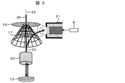
- FIG. 2 shows an example in detail from the orthogonal electromagnetic deflector 20 to the detector 21.
- the electrode 17 for shielding the electron beam 36 from the influence of the electric field generated by the voltage applied by the electric field controller 6 of the detector 21 is disposed.
- the electrode 17 has a conical shape to be rotated, and has a mesh shape so that the information signal 33 can easily pass through.
- the information signal 33 is deflected by the orthogonal electromagnetic deflector 20 so that the information signal 33 can be directly detected by the detector 21. However, the amount of deflection of the information signal 33 may be reduced in order to reduce the influence of the aberration generated when the information signal 33 is deflected.
- the information signal 33 is once applied to the electrode (reflecting plate) 18 used as a reflecting plate, and the second information signal 34 generated from the electrode (reflecting plate) 18 is supplied to the detector 21. It is also possible to guide to the detector 21 with an attractive electric field.
- the electrode 17 is disposed so as to be in close proximity to or in contact with the electrode (reflecting plate) 18, so that the electric field from the detector 21 does not easily leak into the optical axis 43, that is, the electron beam 36 is applied to the electric field of the detector 21. It becomes difficult to be affected. Therefore, the electron beam 36 can suppress the occurrence of axial deviation and aberration.
- the electrode 17 is at ground potential, but as shown in FIG. 4, it is also possible to apply a voltage to the electrode 17 to filter only a certain signal among the information signals 33 from the sample 13.
- the information signal 33 generated from the sample 13 is filtered with respect to energy that is not desired to be detected, so that the information signal 33 can be discriminated, and only the information signal 33 having the energy that is desired to be extracted.
- an image can be formed.
- the voltage applied to the electrode 17 is varied while scanning the sample 13 with the deflector 16, images formed with different energies can be acquired.
- the voltage applied to the electrode 17 is controlled by the control unit 22 via the voltage control unit 19.
- the control unit 22 controls the voltage control unit 19 by linking to the variable deceleration power source 14 that controls the voltage applied to the sample 13. For example, if the voltage applied to the sample 13 is Vr and the energy of the information signal 33 to be filtered is e, the voltage Vt applied to the electrode 17 is controlled by the following equation (1).
- the voltage Vt applied to the electrode 17 may be set to 1.1 kV.
- FIG. 5 shows an example in which the information signal 33 is irradiated to the electrode (reflecting plate) 18 and the second information signal 34 generated from the electrode 18 is detected by the detector 21.
- the control is the same as in FIG.
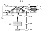
- FIG. 6 shows an example in which a plurality of electrodes 17 are formed.
- FIG. 6 shows a case of three sheets.
- the electrode 17 is basically a composite electrode sandwiched between an electrode 25 and an electrode 26 that are at ground potential.
- the electric field of the electrode 17 is suppressed by the electrode 25 and the electrode 26 which are the ground potential. Therefore, the problem that occurs when the electric field of the electrode 17 is strong can be solved. For example, when the electric field is strong, a lens action that cannot be ignored occurs, and the aberration of the primary beam becomes a problem that the beam is blurred. Moreover, it interferes with the attraction
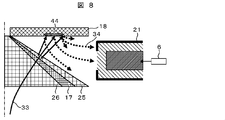
- FIG. 7 shows an example in which the detector 21 directly detects the information signal 33 that has passed through the composite electrode without irradiating the electrode 18.
- the information signal 33 passing through the composite electrode undergoes a lens action within the electrode, and its trajectory changes depending on the energy of the information signal 33 and the incident angle on the electrode 17. That is, the information signal 33 is irradiated with a spread when it is applied to the electrode (reflector) 18.
- the irradiation area 44 varies greatly depending on the energy of the information signal 33 and the voltage applied to the electrode 17.
- the second information signal 34 generated from the electrode (reflecting plate) 18 is also emitted with various angles and energies, if the irradiation area 44 is large, all the second information generated from the irradiation area 44 is generated. It becomes difficult to detect the signal 34 with the detector 21. Therefore, a method of directly detecting the information signal 33 without irradiating the electrode (reflector) 18 as shown in FIG. 7 is effective.
- FIG. 9 shows a conical shape of the electrode (reflecting plate) 18 so that the attraction electric field of the detector 21 is uniform. This shape can be applied to both the case where the information signal 34 is indirectly detected using the electrode 18 and the case where the information signal 33 is directly detected.
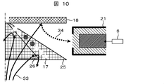
- FIG. 10 includes a plurality of rings with the electrode 17 in a ring shape, and the information signal 33 from the sample 13 can be discriminated by applying a voltage to each ring.
- FIG. 11 shows an example of a plurality of annular electrodes 17. For example, in FIG. 11, there are six rings, and the applied voltage is controlled by voltage controllers a to f in each ring. In one example, a voltage that filters the energy information signal 33 in the voltage control units 19a, 19b, 19e, and 19f is applied, and the voltage control units 19c and 19d have a voltage that allows the information signal 33 to pass through or a ground potential.
- the information signal 33 since the information signal 33 has a different trajectory depending on the emission angle from the sample 13, the information signal 33 can be discriminated by the difference in the trajectory as long as the configuration is as shown in FIG.
- the information signal 33 from the sample 13 spreads widely and enters the electrode 17, it is also possible to detect by providing a plurality of detectors 21. For example, it is possible to discriminate the information signal 33 emitted from the sample 13 by the electrode 17 without operating the orthogonal electromagnetic deflector 20, and in this case, the occurrence of aberrations when the orthogonal electromagnetic deflector 20 is operated. Therefore, signal discrimination can be performed with high resolution. Although not shown in the figure, it is also effective to directly detect the information signal 33 as shown in FIG.
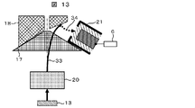
- FIG. 13 shows a configuration example in which the information signal 34 generated from the electrode 18 is made efficient by inclining the electrode (reflecting plate) 18 and further providing the detector 21 with an angle.
- the cross-sectional shape of the energy filter illustrated in FIG. 2 and the like (the shape seen from the vertical direction of the electron beam path) is formed so that the distance from the electrode 18 gradually becomes narrower as it approaches the electron beam path. . Further, they are formed symmetrically about the electron beam path as the central axis.
- the filter is inclined to minimize the bending angle ⁇ due to EXB. Thereby, it becomes possible to suppress the aberration generated by operating EXB.
- FIG. 6 by configuring the mesh electrode so that the angle formed by the electrode 26 having the ground potential and the electrode 18 (which may be the detection surface of the detector) is an acute angle, FIG. It is possible to suppress the influence on the beam of the electric field formed by the voltage applied to the electrode 17 without installing the cylindrical electrode 351 that is long in the optical axis direction as exemplified in (a) and (b). Become.
- contamination may adhere to the inside of the cylindrical electrode 315 due to collision of passing electrons, and when charge accumulates in this contamination, the cylindrical electrode may have a deflection action.
- the longer the length of the cylindrical electrode the greater the possibility that contamination will adhere, so it is desirable to make the length of the cylindrical electrode as short as possible.
- the electrode 18 is further away from the optical axis, resulting in a deflection angle by the orthogonal electromagnetic field generator (EXB). Must be set larger. Further, if the cylindrical electrode is formed at an angle with respect to the optical axis, the beam trajectory may be affected.
- the electrode 26 and the like constituting the energy filter are formed along a virtual straight line that intersects the beam optical axis.
- orthogonal electromagnetic field deflection is performed. It is desirable that the electrode 26 be disposed on a distance r from the deflection fulcrum of the vessel 20. That is, it is desirable that the electrode 26 be formed in parallel to a circle having a radius r centered on the deflection fulcrum of the orthogonal electromagnetic field deflector 20.
- FIG. 20 is a detailed explanatory diagram of a measurement or inspection system including an SEM.
- This system includes an SEM main body 2001, a control device 2002 of the SEM main body, and an arithmetic processing device 2003.
- the control unit 31 in FIG. 1 and each control device controlled by the control unit 31 correspond to the control device 2002.
- the arithmetic processing unit 2003 processes an optical condition setting unit 2004 that supplies a predetermined control signal to the control unit 2002, a memory 2005 that stores the obtained image information and recipe information, and a detection signal obtained by the SEM.
- An input signal calculation unit 2006 is incorporated.
- the arithmetic processing unit 2003 is connected to an input device 2007 having an input means.
- the display device provided in the input device 2007 displays a GUI (Graphcal User Interface) or the like for displaying an image, an inspection result, or the like to the operator.
- GUI Graphic User Interface
- the electrons emitted from the sample are captured by the detector 21 and converted into a digital signal by an A / D converter built in the control device 2002.
- Image processing according to the purpose is performed by image processing hardware such as a CPU, ASIC, and FPGA incorporated in the arithmetic processing unit 2003.
- the detection signals obtained by the SEM are two-dimensionally arranged to form a two-dimensional image
- the image forming unit 2008 the luminance of the position on the sample based on the detection signal or the image signal
- a signal waveform forming unit 2009 that forms a waveform indicating a change and a signal analysis unit 2010 that analyzes a signal waveform formed by the signal waveform forming unit 2009 are incorporated.
- control and processing in the arithmetic processing unit 2003 can be assigned to a CPU or an electronic computer equipped with a memory capable of storing images and processed and controlled.
- control device 2002 and the arithmetic processing device 2003 in FIG. 20 function as a control system that controls the SEM main body 2001.
- the information signal 33 (for example, two accelerated by the application of a retarding voltage to the sample) is applied to the electrodes 17, 25, and 26 constituting the energy filter depending on the deflection conditions of the orthogonal electromagnetic field deflector 20 and the like.
- the incident angle of the secondary electrons and the reflected electrons changes, and as illustrated in FIG. 25, the resolution of the energy filter changes according to the incident angle ⁇ [°] of the information signal 33 to the filter.
- the energy resolution may be an optimum value under the condition that the information signal 33 is vertically incident on the energy filter unit, although it may vary depending on the formation accuracy of the mesh electrode. Therefore, it is necessary to control the deflection angle ⁇ [°] of the information signal 33 with the orthogonal electromagnetic deflector 20 so as to enter the energy filter vertically or so as to enter the optimum resolution. .
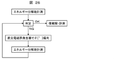
- FIG. 26 shows a flow for controlling the orthogonal electromagnetic deflector 20 so that the energy resolution is the best.
- the energy resolution depends on the energy of the information signal 33 and there is an optimum energy resolution. Accordingly, it is determined whether the measured energy resolution satisfies it. If satisfied, image observation or measurement is started as it is. If not satisfied, the orthogonal electromagnetic deflector 20 deflects the deflection angle ⁇ of the information signal 33 and measures the energy resolution again. These are repeated, and the deflection angle ⁇ is controlled by the orthogonal electromagnetic field deflector 20 so as to obtain the optimum energy resolution.
- the control method of the orthogonal electromagnetic field deflector 20 needs to change the control value depending on the energy of the information signal 33.
- FIG. 28 shows the relationship between the information signal energy and the voltage of the orthogonal electromagnetic deflector 20. It is also possible to control according to a formula obtained by calculation in advance.
- the calculation method of the resolution evaluation index of the energy filter executed by the arithmetic processing unit 2003 will be specifically described.
- the higher the energy resolution the more accurate filtering can be performed.
- a value indicating the superiority or inferiority of the energy resolution performance is defined as a resolution evaluation index.
- SEM optical conditions are set by the optical condition setting unit 2004 (step 2901).
- the optical conditions referred to here are apparatus conditions when the sample is irradiated with the electron beam, such as an acceleration voltage of the electron beam and a retarding voltage applied to the sample.
- the deflection condition of the orthogonal electromagnetic field generator registered in advance in the memory 2005 is set according to the set optical condition (step 2902).
- resolution evaluation is started.
- the voltage Vf applied to the energy filter is changed, and the image forming unit 2008 forms an image based on the detection signal for each predetermined voltage value (step 2903).
- the luminance calculation unit 2011 calculates the luminance (Gray level) of the image based on the formed image (step 2904).
- the determination unit 2012 calculates ⁇ Vf based on the obtained luminance information, and determines whether the ⁇ Vf satisfies a predetermined condition (step 2905).
- ⁇ Vf is calculated by obtaining a change amount of Vf corresponding to a predetermined luminance change amount (Th (u) ⁇ Th (l)) as illustrated in FIG.
- ⁇ Vf or an evaluation value obtained by normalizing ⁇ Vf based on a predetermined condition can be defined as a resolution evaluation index.
- the resolution evaluation index may be obtained based on the calculation of the slope ( ⁇ G / ⁇ Vf) of the correlation curve between the luminance G and Vf. In this case, it can be said that the greater the inclination, the higher the resolution.
- the deflection condition is set as the deflection condition of the orthogonal electromagnetic field generator (step 2907), and when it is determined that the predetermined condition is not satisfied, By changing the set value of the orthogonal electromagnetic field generator (step 2906) and repeating steps 2902 to 2905, an appropriate deflection condition is selected.
- the deflection condition may be selected so that the resolution evaluation index satisfies a predetermined condition when ⁇ Vf is minimum or less than a predetermined value.
- a reference value is set in advance for ⁇ Vf, and a deflection condition in which ⁇ Vf becomes the reference value is selected. good.
- + V EXB and ⁇ V EXB are applied to the two electrodes forming the electrostatic deflector, respectively, and negatively charged electrons are on the electrode side to which + V EXB is applied. To be biased. By rewriting the equation of electron bending angle ⁇ , equation (3) is obtained.
- Vo corresponds to (secondary) information signal energy. If the bending angle ⁇ is determined, the voltage ⁇ V EXB applied to the electrode is determined.
- the optical condition of the electron beam (primary electrons) does not change. Therefore, when it is not desired to change the optical condition, it is desirable to obtain the energy resolution by changing Vf.
- the S curve obtained when the optical condition for example, retarding voltage: Vr
- Vr retarding voltage
- a reference S curve is registered in the memory 2005 in advance, the shift amount is obtained by the signal analysis unit 2010, and V EXB is calculated by the optical condition setting unit 2004. According to an embodiment to be described later, it is possible to obtain a deflection amount corresponding to the charge amount.
- the luminance value changes.
- the optical condition for example, the acceleration voltage of the electron beam, the negative voltage (retarding voltage) applied to the sample, or both
- the luminance value changes.
- the optical condition for example, the acceleration voltage of the electron beam, the negative voltage (retarding voltage) applied to the sample, or both
- the luminance value increases because the number of electrons passing through the energy filter increases as the retarding voltage is gradually increased.
- a resolution evaluation index may be used as an index for finding this condition.
- the amount of change ( ⁇ R) in the retarding voltage corresponding to a predetermined luminance change amount (Th (u) ⁇ Th (l)) or the index value of the evaluation amount is used as the resolution evaluation index.
- the orthogonal electromagnetic field deflector 20 is set to a predetermined condition (step 1701).
- an optical condition for example, applying a retarding voltage
- a predetermined condition for example, applying a retarding voltage
- an electron is emitted from the sample at that time by the detector 21 to acquire an image (step). 1703).
- Luminance information is extracted from this image and stored in a storage medium such as the memory 2005 (step 1704).
- step 1705 By performing the processing of step 1701 to step 1704 for each of a plurality of retarding voltage application conditions, the relationship between the optical condition and the luminance condition as illustrated in FIG. 16 is obtained (step 1705).
- the luminance information detection may be stopped when ⁇ R is detected.
- Steps 1701 to 1705 are performed for a plurality of deflection conditions of the orthogonal electromagnetic deflector 20 (step 1706), ⁇ R is obtained for each of the plurality of deflection conditions, and orthogonal electromagnetic field deflection is performed based on the plurality of ⁇ R.
- the deflection condition of the device 20 is set (step 1707).
- a deflection condition that minimizes ⁇ R when the energy resolution of the energy filter is used in the highest state, it is preferable to select a deflection condition that minimizes ⁇ R.
- a stable measurement condition is always set. Therefore, for example, a reference value is set in advance for ⁇ R, and a deflection condition in which ⁇ R becomes the reference value may be selected. good.
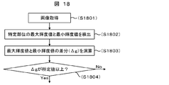
- FIG. 18 shows a process for obtaining the deflection condition of the orthogonal electromagnetic deflector 20 based on the contrast of the image. In this example, steps 1801 to 1804 are applied instead of steps 2903 to 2905 in FIG.
- an image is acquired (step 1801), and the maximum luminance value and the minimum luminance of the region straddling material A (region A) and material B (region B) are acquired.
- a value is detected (step 1802).
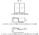
- the region A and the region B can be changed as illustrated in FIG. The brightness difference becomes clear.
- the deflection condition of the orthogonal electromagnetic deflector 20 is not appropriate and the energy resolution is reduced, the energy filtering is not performed properly, and the contrast between the two regions is lowered as illustrated in FIG. 19C, for example. There is a possibility that there is almost no difference in luminance.
- the luminance difference ( ⁇ g) between the two regions is calculated (step 1803), and it is determined whether or not the deflection condition has the largest luminance difference, or whether ⁇ g satisfies the predetermined condition (step 1804).
- the deflection condition is selected assuming that the control of the orthogonal electromagnetic field generator is appropriate (step 2907). If the predetermined condition is not satisfied or the predetermined condition setting has not been completed, the condition of the orthogonal electromagnetic field generator is newly set, and the processing from step 1801 to step 1804 is executed again.
- the selected deflection condition is registered in the memory 2005 or the like as an apparatus condition.
- the determination as to whether or not the luminance difference satisfies a predetermined condition may be made based on, for example, determination as to whether or not a predetermined threshold value is exceeded, and the ratio of two luminance values is a predetermined value. Alternatively, the determination may be made based on the determination of whether the value is less than or equal to the predetermined value.
- the luminance calculation unit 2011 and the determination unit 2012 included in the signal analysis unit 2009 execute the luminance calculation and determination as described above.
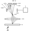
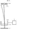
- FIG. 14 is a diagram showing the trajectory of the electrons 1406 emitted from the sample.
- the electrons emitted from the sample 13 are focused by the objective lens, pass through the crossover point 1405, and travel upward (toward the electron source).
- a part of the electrons 1406 emitted from the sample go to the detector 1403 through the energy filter 1404, but the other electrons go in a different direction from the detector 1403 and are not detected.
- an apparatus configuration capable of performing highly accurate energy filtering while improving detection efficiency of detected electrons and maintaining high detection efficiency will be described.
- the SEM illustrated in FIG. 14 is provided with a focusing electrode 1402 as a deflection element that deflects the trajectory of electrons emitted from the sample.
- a focusing electrode 1402 as a deflection element that deflects the trajectory of electrons emitted from the sample.
- the electrons can be directed toward the detector 1403 like the electrons 1407 after the orbital deflection.
- the detector 1403 may be a detector that directly detects electrons, such as an MCP (Micro-Chanel-Plate) detector, or the detector 1403 is a conversion electrode, and a secondary generated from the conversion electrode. You may make it provide the detector which detects an electron separately.
- MCP Micro-Chanel-Plate
- FIG. 15 is a diagram showing a change in luminance value and a change in resolution evaluation index when the applied voltage to the focusing electrode is changed.
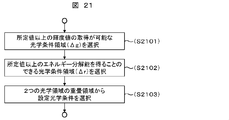
- FIG. 21 is a flowchart showing a process of selecting a voltage to be applied to the focusing electrode 1402 by obtaining the change in the luminance value and the change in the resolution evaluation index.
- two curves are created and two threshold values (Th (g), Th (r)) are set.
- the range ( ⁇ g, ⁇ r) of the applied voltage exceeding the respective threshold values of the two curves is selected (steps 2101 and 2102).
- the applied voltage included in the overlapping region ( ⁇ V) of ⁇ g and ⁇ r is selected as the applied electrode to the focusing electrode 1402 (step 2103).
- the applied voltage region of ⁇ g is a region where the amount of detected electrons is a predetermined value or more, and the applied voltage region of ⁇ r is a region with high energy resolution.
- FIG. 23 is a diagram showing an optical system in which the objective lens 1401 does not form a crossover point 1405 between the detector 1403 and FIG. Even in such an optical system, it is possible to achieve both high-efficiency detection of electrons and optimization of the filtering condition of the energy filter based on the appropriate setting of the focusing electrode 1402, as in the optical system of FIG. Become.
- the orthogonal electromagnetic field deflector 20 deflects the information signal 33 (secondary electrons or the like) from a beam (optical axis of the primary beam without deflection: ideal optical axis) off the axis and the deflection.
- a beam optical axis of the primary beam without deflection: ideal optical axis
- the size of the detection surface of the detector disposed in the vacuum chamber is finite, the detection efficiency decreases when the dispersion is large.
- FIG. 33 is a flowchart showing a process of determining the focusing condition of the focusing lens.
- an image is acquired for each lens intensity set in step 3301 (step 3302), luminance information is extracted from the image, and the detected information has a predetermined condition (for example, the highest luminance value or a predetermined value). Value), the lens strength at that time is selected as the apparatus condition. If the predetermined condition is not satisfied, the lens strength is reset and Steps 3301 to 3304 are repeated.
- FIG. 34 is a flowchart showing the process.
- a lens condition showing a luminance value equal to or higher than a predetermined value for example, Th (g)
- a predetermined value for example, Th (g)
- a lens intensity satisfying a minimum value or a predetermined condition is selected from among a plurality of ⁇ Vf as a lens condition (step 3409).
- the lens condition may be determined only by evaluating the resolution of the energy filter.
Landscapes
- Chemical & Material Sciences (AREA)
- Analytical Chemistry (AREA)
- Analysing Materials By The Use Of Radiation (AREA)
Abstract
本発明は、エネルギーフィルタのエネルギー分解能を向上することを目的とする荷電粒子線装置の提供を目的とする。 上記目的を達成するための一態様として、試料から放出される荷電粒子をエネルギーフィルタに向かって偏向する偏向器を備えた荷電粒子線装置において、当該偏向器の複数の偏向条件ごとに、エネルギーフィルタへの印加電圧を変化させたときに得られる輝度値の変化を求め、当該輝度値の変化が所定の条件を満たす偏向条件を、前記偏向器の偏向条件として設定する荷電粒子線装置を提案する。
Description
本発明は、荷電粒子線装置に係り、特にエネルギーフィルタを通して、特定のエネルギーを持つ荷電粒子を選択的に検出することができる荷電粒子線装置に関する。
荷電粒子線装置の1つである走査電子顕微鏡(Scanning Electron Microscope:SEM)は、微細な対象物に対し、細く絞った電子ビームを走査することによって、試料から二次電子等を放出させ、当該二次電子等に基づいて、微細な対象物の観察,検査、或いは測定等を行う装置である。SEMのエネルギーフィルタは、複数の電極によって構成され、当該複数の電極間に、試料から放出される二次電子等の通過を制限する電界を形成することによって、特定のエネルギーを持つ電子を選択的に検出するために用いられる。特許文献1には、試料から放出された電子をウィーンフィルタによって、光軸から離軸させ当該電子を、エネルギーフィルタを経由して、検出器に導くことが説明されている。また、特許文献2には、試料から放出される電子の軌道を集束する集束素子を設け、軌道修正を行うことによって、二次電子の高効率検出を実現する走査電子顕微鏡が開示されている。更に、特許文献3には、対物レンズに、試料から放出される粒子を減速させるポテンシャル障壁を形成する減速電界電極装置が開示されている。
エネルギーフィルタは、所定値以上のエネルギーを持つ電子を選択的に通過させるためのものであり、或る特定のエネルギー、或いは特定のエネルギー幅の電子が持つ固有の信号情報を取得するためのものである。例えば、低損失(Low loss)の後方散乱電子(Backscattered Electron:BSE)を選択的に検出する場合には、エネルギーフィルタを構成するメッシュ電極に、二次電子(Secondary Electron:SE)が持つエネルギーより、僅かに大きい電圧(負電圧)を印加することによって、試料から放出される電子に多く含まれる二次電子等の検出器への到達を制限する。
一方、エネルギーフィルタは、通常、電子の通過を許容する複数の開口が設けられた複数のメッシュ電極によって構成されているが、その入射方向によっては、エネルギーフィルタのエネルギー分解能が変化することが、発明者らの検討によって明らかになった。
例えば、エネルギーフィルタを構成する板状のメッシュ電極に対し、当該板状体の板状面の垂直方向に近い方向から入射する電子と、板状面に対し鋭角方向から入射する電子を比較すると、後者の電子は、エネルギーフィルタが形成する電界の等電位面に対して斜めの方向から入射することになる。このような入射方向の違いによって、エネルギーフィルタのエネルギー分解能が変動する場合がある。エネルギー分解能とは、エネルギーフィルタの設定条件に対する実際のエネルギーフィルタの性能のばらつきを示す指標である。例えばエネルギーフィルタ電位Vfに対し、実際にエネルギーフィルタを通過する電子のエネルギーの最大値がVf+αであれば、当該エネルギーフィルタは、+α分、余分な電子を通過させていることになる。一方、Vf-αであれば、本来通過させるべき電子を通過させていないことになる。
以上のように、エネルギーフィルタは、電子の入射方向によって、エネルギー分解能が変化し、その入射方向によっては、目的とする観察,検査、或いは測定等が困難になる場合がある。特許文献1~3には、このようなエネルギーフィルタのエネルギー分解能の向上法について何も説明されていない。
以下に、エネルギーフィルタのエネルギー分解能の向上、或いは維持を目的とした荷電粒子線装置について、説明する。
上記目的を達成するための一態様として、エネルギーフィルタに対する荷電粒子の入射方向を変化させる光学素子の条件を変化させて、エネルギーフィルタのエネルギー分解能の評価指標として定義可能な信号を検出する荷電粒子線装置を提案する。
例えば、更に具体的な一態様として、試料から放出される荷電粒子をエネルギーフィルタに向かって偏向する偏向器を備えた荷電粒子線装置において、当該偏向器の複数の偏向条件ごとに、エネルギーフィルタへの印加電圧を変化させたときに得られる輝度値の変化を求め、当該輝度値の変化が所定の条件を満たす偏向条件を、前記偏向器の偏向条件として設定する荷電粒子線装置を提案する。
以上のような構成によれば、エネルギーフィルタを高精度、或いは高安定に使用することができる装置条件を把握することができ、更には当該装置条件に基づく条件設定を行うことが可能となる。
以下の説明は、荷電粒子線装置に係り、特に荷電粒子ビームの照射に基づいて得られる情報を弁別する装置に関する。
荷電粒子線装置には、走査電子顕微鏡(Scanning Electron Microscope:SEM)や、集束イオンビーム(Focused Ion Beam:FIB)装置がある。また、SEMを特定の目的に特化した装置として、測長用電子顕微鏡(Critical Dimension-SEM:CD-SEM)や、上流の検査装置にて得られた欠陥,異物、或いは測長値異常パターンを、更に詳細に観察し、分析するレビュー用電子顕微鏡(レビューSEM)がある。
これらの装置を用いて観察,測定、或いは検査を行う場合、試料からの情報信号を効率良く検出器で検出する必要がある。情報信号が多いことで画質が向上し、それはスループットの向上につながる。しかし、検出率を向上させるために検出器を光軸に近づけたり、情報信号を効率良く検出器まで導入するために検出器に電圧を印加することは、1次ビームへの影響が避けられない。また、これからは見たいもの、つまり検出したいものに応じて情報信号を弁別し、有効な情報のみを抽出することも観察および検査には必要になる。
このように有効な情報を選択的に抽出する装置として、エネルギーフィルタがある。エネルギーフィルタは、試料から放出される荷電粒子の内、特定のエネルギーを持つものを選択的に通過させる装置であり、例えば所望のエネルギーの荷電粒子を検出する場合には、当該エネルギーより低いエネルギーを持つ荷電粒子の通過を制限するための電界を発生する装置である。エネルギーフィルタは例えば、複数のメッシュ電極によって構成され、当該電極への印加電圧を制御することによって、所望の電界を形成する。
一方、このようなエネルギーフィルタは、荷電粒子の入射方向によって、その性能が変化する。即ち、入射方向を適正に設定することができれば、高い性能を発揮することができる。ここで言う性能とはエネルギー分解能のことである。エネルギーフィルタは、入射しようとする電子等に対し、当該電子を追い返すような電界を形成することによって、入射する電子をエネルギー弁別する装置である。このような電界の等電位面に対する電子の入射方向(角度)によっては、フィルタリングされる電子のエネルギーが変化する可能性がある。例えば等電位面に対し、鋭角な方向から入射する電子は、入射方向とは異なる方向から偏向作用を受けるため、等電位面に対して垂直に入射する電子と比較して、エネルギーフィルタを通過することができる電子のエネルギーの上限が低下する可能性がある。
図22は、横軸をエネルギーフィルタに印加する電圧、縦軸をビームの照射部の輝度を示すグラフの一例を示す図であり、第1の方向からエネルギーフィルタに入射する電子を三角で表現し、第2の方向からエネルギーフィルタに入射する電子を丸で表現している。エネルギーフィルタへの印加電圧を徐々に弱めていく(図22の右方向に向かうように)と、検出器によって検出される電子量が増大する。このとき印加電圧Vf〔V〕の変化に対し、輝度が急激に変化する方が、エネルギーフィルタのエネルギー分解能が高いと言える。図22の例では、2つの輝度閾値(Th(u)とTh(l))間の輝度変化を生じさせるVfの変化量が、第1の方向の電子がΔVf1であり、第2の方向の電子がΔVf2である。即ち、図22の例では、第1の方向から入射する電子の方が、第2の方向から入射する電子に対し、エネルギー分解能が高い状態でエネルギーフィルタリングされる。このようにΔVfが小さくなるような装置条件を見出すことによって、入射すべき電子と、入射を制限すべき電子を明確に分離することのできるエネルギー分解能の高いエネルギーフィルタ条件を見出すことができる。
以下、図面を参照してエネルギーフィルタを備えた荷電粒子線装置の一態様であるSEMの概要について説明する。図1は荷電粒子線装置の一例であるSEMの概要を示す図である。なお、以下の説明では走査電子顕微鏡を例にとって説明するが、それに限られることはなく、以下に紹介する実施例は、他の荷電粒子線装置にも、適用が可能である。
試料からの情報信号を効率良く検出器へ導入する際に、検出器に電圧を印加して、情報信号を導入するための吸引電界を発生させることは一般的である。検出効率を向上させるには、その印加電圧を上げるか、検出器を光軸に近づけるかして、吸引電界を強くする方法がとられている。その反面、吸引電界が1次ビームにもおよぼす影響が問題になっている。その影響とは例えば1次ビームの軸ズレ,非点などの収差の発生の要因になる。つまり、情報信号を効率良く検出できるよう、電界を強くすればするほど1次ビームへの影響が大きくなるといったトレードオフの関係にある。
よって、試料から発生した情報信号検出する検出器の吸引電界の影響を少なくし、情報信号を効率良く検出するような検出系を採用することが望ましい。
よって、以下の実施例ではエネルギーフィルタの一態様として、検出器の吸引電界が1次ビームへ影響を及ぼさないようにシールドを配置する例を説明する。また、シールドを複数枚重ねて配置し、いずれかのシールドに電圧を印加することで、試料からの、あるエネルギーを持った信号および試料からの放出角度によって弁別する構成、或いはその他、エネルギー弁別に適した荷電粒子線装置を説明する。
電子銃1は、電子源2,引出電極3、及び加速電極4から構成される。電子源2と引出電極3との間には、引出電圧V1が印加され、これによって、電子源2から電子ビーム36が引き出される。加速電極4はアース電位に維持され、加速電極4と電子源2との間には、加速電圧V0が印加される。したがって電子ビーム36は、この加速電圧V0によって加速される。
加速された電子ビーム36は、絞り15によって不要な領域を除去され、レンズ制御電源5に接続された集束レンズ7および集束レンズ8によって集束される。更に対物レンズ9によって、試料ステージ12上の半導体ウェハ等の試料13に集束される。
試料ステージ12は、ステージ駆動装置23により、少なくとも水平移動可能である。試料13は集束された電子ビーム36によって照射され、走査信号発生器24に接続された偏向器16a,16bによって走査される。このとき非点収差補正器40は非点収差補正制御部45で制御される。電子ビーム36の照射によって試料13から放出される情報信号33(二次電子、及び/又は後方散乱電子等)は、直交電磁界偏向器20で偏向され、検出器21によって検出される。検出された情報信号33は、CRT等の像表示装置32の輝度変調信号とすることで、像表示装置32に試料13の拡大像が表示される。図示はしていないが、以上の構成が電子ビームを照射するのに適した真空容器内に収納される。レンズ制御電源5,走査信号発生器24,非点収差補正制御部41は、制御部31に接続されている。また、直交電磁界偏向器20は、制御部31からの指示により、直交電磁界制御部50によって制御される。なお、直交電磁界偏向器20は、情報信号33を検出器21側に偏向する電界を発生する電極と、当該電界に直交するように、磁界を発生するための磁極を含み、当該磁界は電界によるビームの偏向作用を相殺するように、ビームを偏向する。
図2は直交電磁界偏向器20から検出器21までを詳細にした一例である。光軸43上に、電子ビーム36が検出器21の、電界制御部6によって印加された電圧によって発生する電界の影響を受けないようシールドするための電極17を配置した。例では電極17は回転対象の円錐型で、情報信号33が通過しやすいようにメッシュ状になっている。
情報信号33は検出器21に直接検出できるよう直交電磁界偏向器20で偏向するが、偏向する際に発生する収差の影響を少なくするため、情報信号33の偏向量を小さくする場合もある。そのときは図3に示すように、情報信号33をいったん反射板として利用する電極(反射板)18に照射し、電極(反射板)18から発生する第2の情報信号34を検出器21の吸引電界で検出器21まで導引することも可能である。
電極17は、電極(反射板)18に極接近させるか、または接するよう配置することで、検出器21からの電界が光軸43へ染み出しにくくなり、つまり電子ビーム36が検出器21の電界の影響を受けにくくなる。よって、電子ビーム36は軸ずれや収差の発生を抑制できる。
通常、電極17はアース電位であるが、図4に示すように電極17に電圧を印加して、試料13からの情報信号33のうち、ある信号だけをフィルターをすることも可能である。この構成においては、試料13から発生する情報信号33のうち、検出したくないエネルギーに対してフィルターをすることで、情報信号33の弁別が可能になり、抽出したいエネルギーをもった情報信号33だけで、画像を形成することが可能になる。つまり、偏向器16で試料13を走査しながら、電極17に印加する電圧を可変すれば異なるエネルギーで形成された画像を取得することが可能になる。
また、電極17に印加する電圧は電圧制御部19を介して、制御部22で制御される。制御部22は試料13に印加する電圧を制御する可変減速電源14にリンクして、電圧制御部19を制御することになる。例えば試料13に印加する電圧をVrとし、フィルターしたい情報信号33のエネルギーをeとすると電極17に印加する電圧Vtは次の(1)式で制御される。

試料13に印加する電圧Vrが1kVで、フィルターしたい情報信号33のエネルギーが100eVであれば、電極17に印加する電圧Vtは1.1kVに設定すればよい。
図5は電極(反射板)18に情報信号33を照射し、電極18から発生した第2の情報信号34を検出器21で検出する例である。制御に関しては図4と同様に制御する。
図6は電極17を複数枚で構成した一例である。例として、3枚で構成した場合を図6に示す。電極17は基本的にはアース電位となる電極25と電極26で挟んで複合化電極とする。図4および図5と違い、電極17の電界は、アース電位である電極25と電極26によって抑制される。そのため、電極17の電界が強い場合に発生する問題が解決可能になる。例えば電界が強いと無視できないレンズ作用が発生し、1次ビームの収差となりビームがぼけてしまうといった問題が発生する。また検出器21の吸引電界と干渉し、情報信号33および情報信号34の軌道を変化させてしまう。
図7は複合化電極を通過した情報信号33を電極18に照射せずに、検出器21で直接検出する例を示す。図8に示すように、複合化電極を通過する情報信号33は、電極内のレンズ作用を受けて情報信号33のエネルギーや電極17への入射角度によって、その軌道が変化する。つまり情報信号33は電極(反射板)18に照射されるときに広がりを持って照射される。その照射領域44は情報信号33のエネルギーや、電極17に印加された電圧によって大きく変化する。さらにその電極(反射板)18から発生する第2の情報信号34も様々な角度やエネルギーを持って出射するため、照射領域44が大きいと、その照射領域44から発生したすべての第2の情報信号34を検出器21で検出するのは困難になる。よって、図7に示すように電極(反射板)18に照射することなく、直接、情報信号33と検出する方法が有効である。
図9は検出器21の吸引電界を均一にするように、電極(反射板)18を円錐型にしたものである。この形状は電極18をつかって間接的に情報信号34を検出する場合でも、情報信号33を直接、検出する場合でも両方に適用可能である。
図10は電極17を環状にして複数の環状で構成され、各々の環に電圧を印加することで試料13からの情報信号33を弁別することが可能になる。図11は複数の環状電極17の一例である。例えば図11では6つの環状で構成され、各々の環状に電圧制御部a~fで印加電圧を制御する。一例では電圧制御部19a,19b,19e,19fにあるエネルギーの情報信号33をフィルターする電圧を印加し、電圧制御部19c,19dは情報信号33が通過可能な電圧、またはアース電位とする。
また、情報信号33は試料13からの出射角度によって軌道が違うため、図11のような構成であれば、軌道の違いによる情報信号33の弁別も可能である。
図12のように、試料13からの情報信号33が大きく広がって電極17に入射する場合、検出器21を複数個設けて検出することも可能である。例えば直交電磁界偏向器20を動作させずに、試料13から出射した情報信号33を電極17で弁別することも可能で、この場合は直交電磁界偏向器20を動作させた場合の収差の発生を抑制することができ、高分解能のまま信号弁別が可能になる。また図で示していないが、図9のような直接、情報信号33を検出する場合も有効である。
図13は電極(反射板)18を傾斜させて、更に検出器21にも角度を持たせ、電極18から発生する情報信号34を効率良くする構成例である。
なお、図2等に例示するエネルギーフィルタの断面形状(電子ビーム通路の垂直方向から見た形状)は、電子ビーム通路に近づくに従って、徐々に電極18との間隔が狭くなるように形成されている。また、電子ビーム通路を中心軸とした軸対称に形成されている。
エネルギーフィルタを試料と平行に設置した場合、情報信号はEXBで偏向され、エネルギーフィルタに入射角度θでもって入射する(図35(a))。角度θに依存してエネルギー分解能が悪くなるので図35(b)のように、エネルギーフィルタに垂直入射するために新たにEXB(20b)を設置する方法もあるが、制御が複雑になる。もちろん、EXBを動作させるときに発生する収差はさけられない。
よって、図35(c)のように、フィルターを傾斜させてEXBによる曲げ角θを最小限にする。これにより、EXBを動作させることで発生する収差を抑制することが可能になる。
また、図6等に例示するように、接地電位である電極26と、電極18(検出器の検出面でも良い)の成す角が、鋭角となるようにメッシュ電極を構成することによって、図35(a),(b)に例示するような光軸方向に長い筒状電極351を設置することなく、電極17に印加される電圧によって形成される電界のビームに対する影響を抑制することが可能となる。
筒状電極315の内側には、通過する電子の衝突によって、コンタミネーションが付着する場合があり、このコンタミネーションに電荷が蓄積すると、筒状電極が偏向作用を持つ場合がある。筒状電極の長さが長い程、コンタミネーションが付着する可能性が増大するため、筒状電極の長さを可能な限り短くすることが望ましい。一方で、コンタミネーションの付着を防止すべく、筒状電極の径を大きくすると、その分、電極18が、光軸より離間することになり、結果として直交電磁界発生器(EXB)による偏向角を大きく設定する必要がある。また、筒状電極が僅かでも光軸に対して斜めに形成されていると、ビーム軌道に影響を与える可能性もある。
図6等に例示するエネルギーフィルタによれば、筒状電極に換えて、電極26と電極18によって負電圧が印加される電極17を包囲するような構成(即ち、電極26の端部と電極18の端部を接続し、2つの電極の成す角が鋭角となるようにする)することによって、筒状電極がビームにもたらす影響を抑制することが可能となる。
なお、図6の例では、エネルギーフィルタを構成する電極26等は、ビーム光軸に交差する仮想直線に沿って形成されているが、エネルギーフィルタの分解能をより高めるためには、直交電磁界偏向器20の偏向支点からの距離r上に電極26が配置されることが望ましい。即ち、直交電磁界偏向器20の偏向支点を中心とした半径rの円に平行に、電極26が形成されることが望ましい。
このような構成によれば、偏向支点と電極を結ぶ直線が、電極26の法線となるため、直交電磁界偏向器20の偏向角によらず、高い分解能のエネルギーフィルタリングを行うことが可能となる。
図20は、SEMを含む測定、或いは検査システムの詳細説明図である。本システムには、SEM本体2001,当該SEM本体の制御装置2002、及び演算処理装置2003が含まれている。図1の制御部31及び当該制御部31によって制御される各制御装置は、制御装置2002に相当する。
演算処理装置2003には、制御装置2002に所定の制御信号を供給する光学条件設定部2004、得された画像情報や、レシピ情報を記憶するメモリ2005、及びSEMによって得られた検出信号を処理する入力信号演算部2006が内蔵されている。
更に演算処理装置2003は、入力手段を備えた入力装置2007と接続されている。入力装置2007に設けられた表示装置には、操作者に対して画像や検査結果等を表示するGUI(Graphcal User Interface)等が表示される。
試料から放出された電子は、検出器21にて捕捉され、制御装置2002に内蔵されたA/D変換器でデジタル信号に変換される。演算処理装置2003に内蔵されるCPU,ASIC,FPGA等の画像処理ハードウェアによって、目的に応じた画像処理が行われる。入力信号演算部2007には、SEMによって得られた検出信号を二次元的に配列して二次元像を形成する画像形成部2008,検出信号、或いは画像信号に基づいて試料上の位置に対する輝度の変化を示す波形を形成する信号波形形成部2009、及び当該信号波形形成部2009にて形成された信号波形を解析する信号解析部2010が内蔵されている。
なお、演算処理装置2003における制御や処理の一部又は全てを、CPUや画像の蓄積が可能なメモリを搭載した電子計算機等に割り振って処理・制御することも可能である。本例の場合、図20の制御装置2002と演算処理装置2003は、SEM本体2001を制御する制御システムとして機能する。
図24に示すように、直交電磁界偏向器20等の偏向条件によって、エネルギーフィルタを構成する電極17,25,26への情報信号33(例えば試料へのリターディング電圧の印加によって加速される二次電子や反射電子)の入射角度が変化し、図25に例示するように、エネルギーフィルタの分解能は情報信号33のフィルターへの入射角θ[°]に応じて変化する。メッシュ状電極の形成精度等に応じて変化する場合があるが、エネルギー分解能が最適値になるのは、エネルギーフィルタ部に情報信号33が垂直に入射する条件である。よって直交電磁界偏向器20で情報信号33の偏向角θ[°]を制御して、エネルギーフィルタへ垂直に入射するか、または最適分解能になるように入射するように制御することが必要になる。
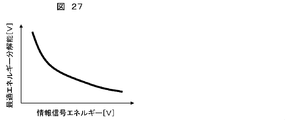
図26に、エネルギー分解能が最良になるように直交電磁界偏向器20を制御する場合のフローを示す。最初にエネルギー分解能の計測を行う。エネルギー分解能は、例えば図27に示すように、情報信号33のエネルギーに依存して最適エネルギー分解能が存在する。それに従って、計測されたエネルギー分解能がそれを満足しているかどうかを判定する。満足していれば、そのまま像観察または計測が開始される。満足していない場合は、直交電磁界偏向器20で情報信号33の偏向角θを偏向して、再度エネルギー分解能を計測する。それらを繰り返して、最適エネルギー分解能になるように直交電磁界偏向器20で偏向角θを制御する。
直交電磁界偏向器20の制御方法は、情報信号33のエネルギーに依存して制御値を変化させる必要がある。図28に情報信号エネルギーと直交電磁界偏向器20の電圧の関係を示す。予め計算によって求められた式に従って、制御することも可能である。
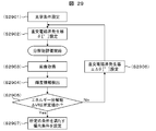
以下に、演算処理装置2003にて実行されるエネルギーフィルタの分解能評価指標の算出法を具体的に説明する。図22を用いて説明したように、エネルギー分解能が高い程、高精度なフィルタリングを行うことができる。本実施例では、このようなエネルギー分解能の性能の優劣を示す値を、分解能評価指標として定義する。このような分解能評価指標の算出に基づく、直交電磁界発生器の制御法について、図29のフローチャートを用いて説明する。
まず、光学条件設定部2004によって、SEMの光学条件を設定する(ステップ2901)。ここで言う光学条件とは、電子ビームの加速電圧,試料に印加するリターディング電圧等、電子ビームを試料に対して照射する際の装置条件である。次に、設定された光学条件に応じて予めメモリ2005に登録されている直交電磁界発生器の偏向条件を設定する(ステップ2902)。以上のような条件のもと、分解能評価を開始する。エネルギーフィルタに印加する電圧Vfを変化させ、画像形成部2008は、所定の電圧値ごとに、検出信号に基づいて画像を形成する(ステップ2903)。輝度演算部2011では、形成された画像に基づいて、画像の輝度(Gray level)を演算する(ステップ2904)。判定部2012では、得られた輝度情報に基づいて、ΔVfを演算し、当該ΔVfが所定の条件を満たしているか否かの判定を行う(ステップ2905)。
ここで、ΔVfは、図22に例示されているように、所定の輝度変化量(Th(u)-Th(l))に対応するVfの変化量を求めることによって算出する。先述したように、この変化量が小さい程、エネルギーフィルタの分解能が高いと言える。よって、ΔVf、或いはΔVfを所定の条件に基づいて正規化した評価値を、分解能評価指標として定義することができる。なお、輝度GとVfの相関曲線の傾き(ΔG/ΔVf)の算出に基づいて、分解能評価指標を求めるようにしても良い。この場合、傾きが大きい程、分解能が高いと言える。
分解能評価指標が所定の条件を満たすと判断できる場合には、その偏向条件を直交電磁界発生器の偏向条件として設定し(ステップ2907)、所定の条件を満たさないと判断される場合には、直交電磁界発生器の設定値を変化させ(ステップ2906)、ステップ2902~2905を繰り返すことによって、適正な偏向条件を選択する。なお、ΔVfが分解能評価指標である場合には、ΔVfが最小、或いは所定値未満である場合に、分解能評価指標が所定の条件を満たすものとして、偏向条件を選択すると良い。また、半導体パターンを測定するSEMでは、常に安定した測定条件の設定が求められるため、例えばΔVfについて予め参照値を設定しておき、ΔVfが当該参照値となる偏向条件を選択するようにしても良い。
図29に例示するようなプロセスに基づいて偏向条件を設定することによって、試料の帯電状態やその他の電子の軌道の変動要因によって変化する適正な偏向条件を見出すことが可能となる。
なお、図直交電磁界発生器の内、電界(E)による偏向量をyとすると式(2)が成り立つ。

d:静電偏向器の電極間の距離
L1:偏向始点と、電子が偏向量y分偏向される位置との距離
VEXB:静電偏向器に印加する電圧
図30(a)に例示するように、静電偏向器を形成する2枚の電極にはそれぞれ+VEXB,-VEXBが印加され、負電荷を持つ電子は、+VEXBが印加された電極側に偏向される。電子の曲げ角θの式になおすと式(3)のようになる。

Voに相当するのは、(二次)情報信号エネルギーであり、曲げ角θが決まれば、電極にかける電圧±VEXBが決まる。
また、図30(b)に例示するような直交電磁界発生器の磁界Bと偏向量yの式は(4)で表される。

曲げ角θの式になおすと式(5)のようになる。

B:電子の電荷(1.6021×10⁻¹⁹C)
lB:磁界範囲
これらの式を解いて、1次ビームは偏向しないで二次信号(試料から放出される電子)のみ偏向する条件をみつける。
このような条件を、偏向角θごとに求めることによって、図30(c)に例示するような試料から放出される電子のエネルギーと、偏向器に与える電圧(電流)との関係を求めることができ、二次信号の偏向角に応じた1次ビームを偏向させない条件を見出すことが可能となる。このような条件は、メモリ2005に登録され、直交電磁界発生器への制御信号として、光学条件設定部2004によって設定される。
図29の例では、複数の偏向角ごとに、分解能評価指標を求める際に、エネルギーフィルタに印加する電圧Vfを変化させることによって、輝度とVfとの相関曲線(Sカーブ)を偏向角ごとに検出する例について説明したが、Sカーブを、光学条件を変化させることによって形成することも可能である。
なお、Vfを変化させても電子ビーム(一次電子)の光学条件は変化しないため、光学条件を変えたくない場合には、Vfを変化させることによって、エネルギー分解能を求めることが望ましい。一方で、光学条件(例えばリターディング電圧:Vr)を変化させたときに得られるSカーブは、輝度-Vr相関曲線のグラフ上、試料に付着した帯電分、+Vr、或いは-Vr側にシフトしたカーブとなる。即ち、帯電のないときのSカーブが判っていれば、そのシフト量を求めることで、帯電量を計測することが可能となる。このような帯電量の計測に基づいて、VEXBを求めることによって、適正な偏向強度を求めることが可能となる。この場合、予めメモリ2005に基準Sカーブを登録しておき、信号解析部2010によって、シフト量を求め、光学条件設定部2004によって、VEXBを算出する。後述する実施例によれば、帯電量に応じた偏向量を求めることが可能となる。
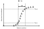
例えば、図16に例示するように、光学条件(例えば、電子ビームの加速電圧,試料に印加する負電圧(リターディング電圧)、或いはその両方)を変化させると、輝度値が推移する。例えば光学条件がリターディング電圧である場合、リターディング電圧を徐々に大きくしていくと、エネルギーフィルタを通過する電子の数が増えていくため、輝度値が増大する。
先に説明したように、この変化が急峻である程、エネルギー分解能が高い。よって、この条件を見出すための指標として、分解能評価指標を用いると良い。図16の例では、所定の輝度変化量(Th(u)-Th(l))に対応するリターディング電圧の変化量(ΔR)、或いは当該評価量の指標値を、分解能評価指標としている。この評価指標に基づいて、エネルギーフィルタの高精度化、或いは高安定化を実現するSEMの装置条件設定工程を図17に例示するフローチャートを用いて説明する。
本例では、図2,図3等に例示する直交電磁界偏向器20の偏向条件の適正化に基づいて、エネルギーフィルタのエネルギー分解能を向上、或いは安定化させる例について説明する。先ず、直交電磁界偏向器20を所定の条件に設定する(ステップ1701)。この状態で所定の条件に光学条件(例えばリターディング電圧印加)を設定し(ステップ1702)、その際に試料から放出される電子を検出器21にて検出することによって、画像を取得する(ステップ1703)。この画像から輝度情報を抽出し、メモリ2005等の記憶媒体に記憶させる(ステップ1704)。このステップ1701~ステップ1704の処理を複数のリターディング電圧印加条件ごとに実施することによって、図16に例示するような光学条件と輝度条件との関係を求める(ステップ1705)。なお、本例では所定数の光学条件について輝度を求める例を説明しているが、ΔRが検出された時点で輝度情報検出を停止するようにしても良い。
ステップ1701~ステップ1705の処理を直交電磁界偏向器20の複数の偏向条件について実施し(ステップ1706)、複数の偏向条件ごとにΔRを取得し、当該複数のΔRに基づいて、直交電磁界偏向器20の偏向条件を設定する(ステップ1707)。ここで、エネルギーフィルタのエネルギー分解能を最も高い状態で用いる場合には、ΔRが最も小さくなる偏向条件を選択すると良い。一方、半導体パターンを測定するSEMでは、常に安定した測定条件の設定が求められるため、例えばΔRについて予め参照値を設定しておき、ΔRが当該参照値となる偏向条件を選択するようにしても良い。
また、図29に例示するフローチャートでは、直交電磁界偏向器20の偏向条件ごとに、ΔVfを求める例を、図17に例示するフローチャートでは、直交電磁界偏向器20の偏向条件毎に、ΔRを求める例について説明したが、例えば図19に例示するように、SEMの視野(Field Of View:FOV)内に2種以上の材質からなる試料が含まれており、エネルギーフィルタリングが適正に行われれば、2種の材質間で明確にコントラストが現れるような場合に、両者間のコントラストに基づいて、適正な偏向条件を求めることも可能である。以下、その例について説明する。図18は、画像のコントラストに基づいて、直交電磁界偏向器20の偏向条件を求めるための工程を示すものである。本例では図29のステップ2903~ステップ2905に替えて、ステップ1801~ステップ1804を適用する。
直交電磁界偏向器20の偏向条件を所定の条件に設定した後、画像を取得し(ステップ1801)、材質A(領域A)と材質B(領域B)に跨る領域の最大輝度値と最小輝度値を検出する(ステップ1802)。このとき、エネルギーフィルタへの印加電圧が適切であり、且つ直交電磁界偏向器20の偏向条件が適切なものであれば、図19(b)に例示するように、領域Aと領域Bとの輝度差が明確になる。一方、直交電磁界偏向器20の偏向条件が適切ではなく、エネルギー分解能が低下すると、エネルギーフィルタリングが適正に行われず、例えば図19(c)に例示するように、2つの領域のコントラストが低下し、輝度差が殆どない状態となる可能性がある。
そこで、本例では2つの領域の輝度差(Δg)を算出(ステップ1803)し、当該輝度差が最も大きい偏向条件、或いはΔgが所定の条件を満たす偏向条件か否かを判定(ステップ1804)。ここで、Δgが所定値以上、或いは所定条件を満たす場合には、直交電磁界発生器の制御が適正なものであるとして、当該偏向条件を選択する(ステップ2907)。また、所定条件を満たさない場合や所定の条件設定が終わっていない場合には、直交電磁界発生器の条件を新たに設定して、ステップ1801~ステップ1804の処理を再実行する。選択された偏向条件は、装置条件としてメモリ2005等に登録する。
以上のような構成によれば、2以上の領域間のコントラストを明確にすることによって、所望の測定対象の測定を行うような場合に、適切な偏向条件を選択することが可能となる。なお、輝度差が所定の条件を満たすか否かの判定は、例えば所定の閾値を超えるか否かの判定に基づいて、行うようにしても良いし、2つの輝度値の比が所定の値、或いは所定値未満、または以上となるかの判定に基づいて、行うようにしても良い。これらの輝度差や輝度比、或いはその指標値を分解能評価指標とすることによって、目的とする測定や検査を行うための装置条件を適正に評価することが可能となる。また、輝度変化が急峻なほど、分解能が高いと言えるため、例えば輝度変化を近似関数にてフィッティングし、傾斜の程度を求めることによって、分解能評価指標と定義しても良い。信号解析部2009に含まれる輝度演算部2011や、判定部2012では、上述のような輝度演算や判定を実行する。
これまで、二次電子等を検出器に向かって偏向する偏向器(上述の実施例では直交電磁界偏向器20)を、分解能評価指標に基づいて、設定する例を説明したが、以下に、試料から放出される電子を集束する集束素子を用いて、電子の軌道を偏向することによって、適正な装置条件を設定する例について説明する。図14は、試料から放出された電子1406の軌道を示す図である。試料13から放出された電子は、対物レンズによって集束され、クロスオーバ点1405を通過して、上方(電子源方向)に向かう。試料から放出された電子1406は、一部がエネルギーフィルタ1404を介して、検出器1403に向かうが、その他の電子は、検出器1403とは異なる方向に向かい、検出されない。本例では、検出される電子の検出効率を向上させると共に、高い検出効率を維持した状態で、高精度なエネルギーフィルタリングを行い得る装置構成について説明する。
図14に例示するSEMは、試料から放出される電子の軌道を偏向する偏向素子として、集束電極1402が設けられている。例えばこの集束電極1402に対し、レンズ制御電源5から電圧を印加することによって、軌道偏向後の電子1407のように、検出器1403に向かって電子を方向付けることができる。なお、検出器1403は、MCP(Micro Chanel Plate)検出器のような電子を直接的に検出する検出器であっても良いし、検出器1403を変換電極とし、当該変換電極から生じた二次電子を検出する検出器を別に設けるようにしても良い。
図15は、集束電極への印加電圧を変化させたときの輝度値の変化と、分解能評価指標の変化を示す図である。また、図21は当該輝度値の変化と、分解能評価指標の変化を求めることによって、集束電極1402への印加電圧を選択する工程を示すフローチャートである。本例では、集束電極1402への印加電圧ごとに、輝度値と分解能評価指標を求めることによって、2つのカーブを作成すると共に、2つの閾値(Th(g),Th(r))を設定し、2つのカーブのそれぞれの閾値を超えた印加電圧の範囲(Δg,Δr)を選択する(ステップ2101,2102)。本例では、ΔgとΔrの重畳領域(ΔV)に含まれる印加電圧を、集束電極1402への印加電極として選択する(ステップ2103)。Δgの印加電圧領域は、検出される電子の量が所定値以上の領域であり、Δrの印加電圧領域は、エネルギー分解能が高い領域である。このような2つの印加電圧領域の重畳領域に含まれる電圧を選択することによって、電子の高効率検出と、エネルギーフィルタのフィルタリングコンディションの適正化の両立が可能となる。以上のような処理は、信号解析部2010によって行われる。
図23は、図14とは異なり、対物レンズ1401が検出器1403との間にクロスオーバ点1405を作らない光学系を示す図である。このような光学系であっても、図14の光学系と同様に、集束電極1402の適正な設定に基づいて、電子の高効率検出と、エネルギーフィルタのフィルタリングコンディションの適正化の両立が可能となる。
図31は、直交電磁界偏向器20によって、情報信号33(二次電子等)をビーム(偏向を伴わない1次ビームの光軸:理想光軸)から、軸外に偏向すると共に、当該偏向軌道上にエネルギーフィルタと検出器21を配置した検出系を用いたSEMにて、電子の検出効率の向上を可能とする集束レンズを設けた例を示す図である。試料から放出され、直交電磁界偏向器20によって、軸外に偏向された情報信号33は、図31に例示するように分散する。一方で、真空室内に配置される検出器の検出面の大きさは有限であるため、分散が大きいと、検出効率が低下する。
そこで、本実施例では、直交電磁界偏向器20と検出器25との間に、集束レンズを配置し、情報信号の軌道を制御することで、検出効率の向上を図る手法について説明する。図31に例示するように、集束レンズ(例えば静電レンズ等)の集束作用がないと、理想光軸から離間するように試料から放出された電子の中には、検出器が存在する位置とは異なる方向に向かうものがある。このような電子を集束レンズの集束作用によって、検出器に向かって偏向すると、検出効率を向上することが可能となる。図33は集束レンズの集束条件を決定する工程を示すフローチャートである。このフローチャートでは、ステップ3301にて設定されたレンズ強度ごとに画像を取得し(ステップ3302)、その画像から輝度情報を抽出し、その検出情報が所定の条件(例えば輝度値が最も高い、或いは所定値等)の場合に、その際のレンズ強度を装置条件として選択し、所定の条件を満たさない場合には、レンズ強度を再設定して、ステップ3301~ステップ3304を繰り返す。ステップ3305では、図32に例示するように、輝度値が最大値のときのレンズ強度(本例の場合、静電レンズに印加する電圧値)、或いは輝度値が所定値(本例の場合、輝度値がTh(g)以上)のレンズ強度をレンズ条件として選択する。
このような工程を経て、レンズ条件を決定することによって、高効率検出の可能な検出系光学条件を設定することが可能となる。
また、エネルギーフィルタリングを行って電子を検出する場合、検出効率が大きい程、良いというわけではない場合がある。例えば、集束レンズの強度を強くする(ビームの開き角を大きくする)と、エネルギーフィルタの電極面に対し、斜めの方向から電子が入射することになるため、エネルギー分解能が低下する可能性がある。そこで、所定の検出量を得ることのできるレンズ条件範囲の中から、エネルギー分解能の高いレンズ条件を見出す手法を提案する。図34はその工程を示すフローチャートである。図33の検出工程において、所定値(例えばTh(g))以上の輝度値を示すレンズ条件が見出されたときに、そのレンズ強度範囲の中から適正なレンズ強度を選択すべく、複数のレンズ条件において、図22に例示するようなSカーブを形成し、ΔVfを求める(ステップ3402~ステップ3407)。
ここで、複数のΔVfの中から最小値、或いは所定の条件を満たすレンズ強度をレンズ条件として選択する(ステップ3409)。
以上のような構成によれば、十分な電子検出量を確保しつつ、エネルギーフィルタのエネルギー分解能の向上を実現することが可能となる。なお、予め電子検出量が十分に確保できていることが判明している場合には、エネルギーフィルタの分解能評価のみを行うことによって、レンズ条件決定するようにしても良い。
なお、図31に例示するエネルギーフィルタを形成する電極を、直交電磁界偏向器20の偏向支点を中心とした半径rの円に平行に形成することによって、エネルギー分解能を更に高めることが可能となる。
1 電子銃
2 電子源
3 引出電極
4 加速電極
5 レンズ制御電源
6 電界制御部
7,8 集束レンズ
9 対物レンズ
10 クロスオーバ
11 位置モニター用測定装置
12 試料ステージ
13 試料
14 可変減速電源
15 絞り
16a,16b 偏向器
17,18 電極
19 電圧制御部
20 直交電磁界偏向器
21 検出器
22,31,41 制御部
23 ステージ駆動装置
24 走査信号発生器
27 記憶部
32 像表示装置
33,34 情報信号
36 電子ビーム
37 画像処理部
40 非点収差補正器
43 光軸
44 照射領域
2 電子源
3 引出電極
4 加速電極
5 レンズ制御電源
6 電界制御部
7,8 集束レンズ
9 対物レンズ
10 クロスオーバ
11 位置モニター用測定装置
12 試料ステージ
13 試料
14 可変減速電源
15 絞り
16a,16b 偏向器
17,18 電極
19 電圧制御部
20 直交電磁界偏向器
21 検出器
22,31,41 制御部
23 ステージ駆動装置
24 走査信号発生器
27 記憶部
32 像表示装置
33,34 情報信号
36 電子ビーム
37 画像処理部
40 非点収差補正器
43 光軸
44 照射領域
Claims (7)
- 荷電粒子源と試料に対する当該荷電粒子源から放出されるビームの照射に基づいて得られる荷電粒子を検出する検出器と、前記試料から放出される荷電粒子をエネルギーフィルタリングするエネルギーフィルタを備えた荷電粒子線装置において、
前記試料から放出される荷電粒子の前記エネルギーフィルタへの入射方向を調整する偏向素子を備え、前記検出器は、当該偏向素子の異なる偏向条件ごとに、前記荷電粒子を検出することを特徴とする荷電粒子線装置。 - 請求項1において、
前記偏向素子は、前記試料から放出される荷電粒子を偏向する偏向器、或いは前記試料から放出される荷電粒子を集束する集束素子であることを特徴とする荷電粒子線装置。 - 請求項2において、
前記偏向器は、直交電磁界発生器であることを特徴とする荷電粒子線装置。 - 請求項2において、
前記偏向器、或いは集束素子の偏向条件ごとに、前記エネルギーフィルタに印加する電圧、或いは荷電粒子線装置の光学条件を変化させる制御装置を備えたことを特徴とする荷電粒子線装置。 - 請求項4において、
前記制御装置は、前記エネルギーフィルタへの印加電圧ごと、或いは前記光学条件ごとに前記検出器の信号量を検出することを特徴とする荷電粒子線装置。 - 請求項5において、
前記制御装置は、前記エネルギーフィルタへの印加電圧、或いは光学条件を変化させたときの前記信号量の変化が、所定の条件を満たす前記偏向条件、或いは当該信号量の変化が最も急峻な偏向条件を前記偏向器、或いは集束素子の条件として選択することを特徴とする荷電粒子線装置。 - 荷電粒子源と試料に対する当該荷電粒子源から放出されるビームの照射に基づいて得られる荷電粒子を検出する検出器と、前記試料から放出される荷電粒子をエネルギーフィルタリングするエネルギーフィルタを備えた荷電粒子線装置において、
前記試料に負電位を印加する負電圧印加電源と、
前記試料から放出される荷電粒子の前記エネルギーフィルタへの入射方向を調整する偏向素子を備え、
前記偏向素子による偏向条件ごとに、前記負電圧を変化させたときの信号量の変化を検出し、当該変化が所定の条件を満たす前記偏向条件を、前記偏向素子の偏向条件として選択する制御装置を備えたことを特徴とする荷電粒子線装置。
Priority Applications (2)
| Application Number | Priority Date | Filing Date | Title |
|---|---|---|---|
| US14/126,792 US8946649B2 (en) | 2011-06-16 | 2012-04-16 | Charged particle beam device having an energy filter |
| US14/573,965 US9318299B2 (en) | 2011-06-16 | 2014-12-17 | Charged particle beam device having an energy filter |
Applications Claiming Priority (2)
| Application Number | Priority Date | Filing Date | Title |
|---|---|---|---|
| JP2011133793A JP5663412B2 (ja) | 2011-06-16 | 2011-06-16 | 荷電粒子線装置 |
| JP2011-133793 | 2011-06-16 |
Related Child Applications (2)
| Application Number | Title | Priority Date | Filing Date |
|---|---|---|---|
| US14/126,792 A-371-Of-International US8946649B2 (en) | 2011-06-16 | 2012-04-16 | Charged particle beam device having an energy filter |
| US14/573,965 Continuation US9318299B2 (en) | 2011-06-16 | 2014-12-17 | Charged particle beam device having an energy filter |
Publications (1)
| Publication Number | Publication Date |
|---|---|
| WO2012172720A1 true WO2012172720A1 (ja) | 2012-12-20 |
Family
ID=47356741
Family Applications (1)
| Application Number | Title | Priority Date | Filing Date |
|---|---|---|---|
| PCT/JP2012/002606 Ceased WO2012172720A1 (ja) | 2011-06-16 | 2012-04-16 | 荷電粒子線装置 |
Country Status (3)
| Country | Link |
|---|---|
| US (2) | US8946649B2 (ja) |
| JP (1) | JP5663412B2 (ja) |
| WO (1) | WO2012172720A1 (ja) |
Cited By (2)
| Publication number | Priority date | Publication date | Assignee | Title |
|---|---|---|---|---|
| WO2016092642A1 (ja) * | 2014-12-10 | 2016-06-16 | 株式会社 日立ハイテクノロジーズ | 荷電粒子線装置 |
| WO2019021454A1 (ja) * | 2017-07-28 | 2019-01-31 | 株式会社 日立ハイテクノロジーズ | 荷電粒子線装置 |
Families Citing this family (22)
| Publication number | Priority date | Publication date | Assignee | Title |
|---|---|---|---|---|
| JP5663412B2 (ja) * | 2011-06-16 | 2015-02-04 | 株式会社日立ハイテクノロジーズ | 荷電粒子線装置 |
| DE102013006535B4 (de) * | 2013-04-15 | 2025-11-06 | Carl Zeiss Microscopy Gmbh | Raster-Partikelstrahlmikroskop mit energiefilterndem Detektorsystem |
| JP6230831B2 (ja) * | 2013-07-08 | 2017-11-15 | 株式会社日立ハイテクノロジーズ | 荷電粒子線装置および画像取得方法 |
| WO2016121009A1 (ja) | 2015-01-28 | 2016-08-04 | 株式会社 日立ハイテクノロジーズ | 荷電粒子線装置 |
| WO2016142481A1 (en) * | 2015-03-10 | 2016-09-15 | Vladimir Petrovich Ovsyannikov | Method and device for the production of highly charged ions |
| SG11201707201SA (en) | 2015-03-24 | 2017-10-30 | Kla Tencor Corp | Method and system for charged particle microscopy with improved image beam stabilization and interrogation |
| CN107408485B (zh) * | 2015-03-24 | 2020-03-13 | 科磊股份有限公司 | 用于具有改进的图像束稳定性及询问的带电粒子显微镜的方法及系统 |
| DE102015210893B4 (de) * | 2015-06-15 | 2019-05-09 | Carl Zeiss Microscopy Gmbh | Analyseeinrichtung zur Analyse der Energie geladener Teilchen und Teilchenstrahlgerät mit einer Analyseeinrichtung |
| JP2017016755A (ja) | 2015-06-29 | 2017-01-19 | 株式会社日立ハイテクノロジーズ | 荷電粒子線装置 |
| JP6714147B2 (ja) * | 2017-03-24 | 2020-06-24 | 株式会社日立ハイテク | 荷電粒子線装置、及び荷電粒子線装置の調整方法 |
| DE112017007771B4 (de) * | 2017-08-24 | 2023-03-02 | Hitachi High-Technologies Corporation | Vorrichtung für strahl geladener teilchen und beobachtungsverahren und elementanalyseverfahren unter verwendung derselben |
| JP2019164886A (ja) * | 2018-03-19 | 2019-09-26 | 株式会社日立ハイテクノロジーズ | ビーム照射装置 |
| US11211224B2 (en) * | 2018-04-26 | 2021-12-28 | Hitachi High-Tech Corporation | Charged particle beam apparatus |
| US10770262B1 (en) * | 2018-05-30 | 2020-09-08 | National Technology & Engineering Solutions Of Sandia, Llc | Apparatus, method and system for imaging and utilization of SEM charged particles |
| US11139142B2 (en) | 2019-05-23 | 2021-10-05 | Applied Materials, Inc. | High-resolution three-dimensional profiling of features in advanced semiconductor devices in a non-destructive manner using electron beam scanning electron microscopy |
| JP7250661B2 (ja) | 2019-10-31 | 2023-04-03 | 株式会社日立ハイテク | 荷電粒子線装置 |
| US12525430B2 (en) * | 2020-04-28 | 2026-01-13 | Hitachi High-Tech Corporation | Charged particle beam apparatus |
| JP7379712B2 (ja) * | 2020-07-20 | 2023-11-14 | 株式会社日立ハイテク | エネルギーフィルタ、およびそれを備えたエネルギーアナライザおよび荷電粒子ビーム装置 |
| DE102021112503B4 (de) * | 2021-05-12 | 2025-03-27 | Carl Zeiss Microscopy Gmbh | Teilchenstrahlvorrichtung mit einer Ablenkeinheit |
| US11749495B2 (en) | 2021-10-05 | 2023-09-05 | KLA Corp. | Bandpass charged particle energy filtering detector for charged particle tools |
| KR20230068893A (ko) * | 2021-11-11 | 2023-05-18 | 삼성전자주식회사 | 주사 전자 현미경(Scannig Electron Microscope, 이하 SEM), SEM을 동작시키는 방법 및 이를 이용한 반도체 소자를 제조하는 방법 |
| JPWO2025069194A1 (ja) | 2023-09-26 | 2025-04-03 |
Citations (3)
| Publication number | Priority date | Publication date | Assignee | Title |
|---|---|---|---|---|
| JP2001357808A (ja) * | 2000-06-14 | 2001-12-26 | Hitachi Ltd | 回路パターン検査装置および方法 |
| JP2002524827A (ja) * | 1998-09-03 | 2002-08-06 | ケーエルエー−テンカー コーポレイション | 走査型電子ビーム顕微鏡 |
| JP2012003902A (ja) * | 2010-06-15 | 2012-01-05 | Hitachi High-Technologies Corp | 走査型電子顕微鏡及びその制御方法 |
Family Cites Families (32)
| Publication number | Priority date | Publication date | Assignee | Title |
|---|---|---|---|---|
| JP2642881B2 (ja) * | 1994-09-28 | 1997-08-20 | 東京大学長 | 低速多価イオンによる超高感度水素検出法 |
| EP0853243A3 (en) * | 1997-01-13 | 1999-07-28 | Schlumberger Technologies, Inc. | Method and apparatus for detecting defects in wafers |
| GB9719417D0 (en) * | 1997-09-13 | 1997-11-12 | Univ York | Electron microscope |
| JP3724949B2 (ja) * | 1998-05-15 | 2005-12-07 | 株式会社東芝 | 基板検査装置およびこれを備えた基板検査システム並びに基板検査方法 |
| JP4236742B2 (ja) * | 1998-10-29 | 2009-03-11 | 株式会社日立製作所 | 走査形電子顕微鏡 |
| US6252412B1 (en) * | 1999-01-08 | 2001-06-26 | Schlumberger Technologies, Inc. | Method of detecting defects in patterned substrates |
| EP1063677B1 (en) * | 1999-06-23 | 2005-03-16 | ICT Integrated Circuit Testing Gesellschaft für Halbleiterprüftechnik mbH | Charged particle beam device |
| EP1100112A1 (en) | 1999-11-12 | 2001-05-16 | Advantest Corporation | Spectrometer objective for particle beam measuring system |
| JP2001283763A (ja) * | 2000-03-31 | 2001-10-12 | Mamoru Nakasuji | フィルター、電子線装置及びこれらの装置を用いたデバイス製造方法 |
| US6847038B2 (en) * | 2002-07-15 | 2005-01-25 | Hitachi, Ltd. | Scanning electron microscope |
| DE10237141A1 (de) * | 2002-08-13 | 2004-02-26 | Leo Elektronenmikroskopie Gmbh | Strahlführungssystem, Abbildungsverfahren und Elektronenmikroskopiesystem |
| US6797955B1 (en) * | 2003-01-30 | 2004-09-28 | Kla-Tencor Technologies Corporation | Filtered e-beam inspection and review |
| JP2005004995A (ja) * | 2003-06-09 | 2005-01-06 | Hitachi High-Technologies Corp | 走査形電子顕微鏡 |
| US6979824B1 (en) * | 2003-06-26 | 2005-12-27 | Kla-Tencor Technologies Corporation | Filtered e-beam inspection and review |
| EP1605492B1 (en) * | 2004-06-11 | 2015-11-18 | ICT Integrated Circuit Testing Gesellschaft für Halbleiterprüftechnik mbH | Charged particle beam device with retarding field analyzer |
| EP1703537B9 (en) | 2005-03-17 | 2008-10-22 | ICT Integrated Circuit Testing Gesellschaft für Halbleiterprüftechnik mbH | Analysing system and charged particle beam device |
| WO2008010777A1 (en) * | 2006-07-21 | 2008-01-24 | National University Of Singapore | A multi-beam ion/electron spectra-microscope |
| JP5271491B2 (ja) * | 2006-10-26 | 2013-08-21 | 株式会社日立ハイテクノロジーズ | 電子線応用装置および試料検査方法 |
| WO2008101714A2 (en) | 2007-02-22 | 2008-08-28 | Applied Materials Israel, Ltd. | High throughput sem tool |
| JP5075431B2 (ja) * | 2007-02-28 | 2012-11-21 | 株式会社日立ハイテクノロジーズ | 帯電測定方法、焦点調整方法、及び走査電子顕微鏡 |
| US7714287B1 (en) * | 2008-06-05 | 2010-05-11 | Kla-Tencor Corporation | Apparatus and method for obtaining topographical dark-field images in a scanning electron microscope |
| JP2010055756A (ja) * | 2008-08-26 | 2010-03-11 | Hitachi High-Technologies Corp | 荷電粒子線の照射方法及び荷電粒子線装置 |
| JP5250350B2 (ja) * | 2008-09-12 | 2013-07-31 | 株式会社日立ハイテクノロジーズ | 荷電粒子線応用装置 |
| US20120119087A1 (en) * | 2009-08-03 | 2012-05-17 | Hitachi High-Technologies Corporation | Charged-particle microscope |
| US8624186B2 (en) * | 2010-05-25 | 2014-01-07 | Hermes Microvision, Inc. | Movable detector for charged particle beam inspection or review |
| EP2405460B1 (en) * | 2010-07-09 | 2013-02-20 | ICT Integrated Circuit Testing Gesellschaft für Halbleiterprüftechnik mbH | Electron beam device with tilting and dispersion compensation, and method of operating same |
| US8481962B2 (en) * | 2010-08-10 | 2013-07-09 | Fei Company | Distributed potential charged particle detector |
| US8334508B1 (en) * | 2011-02-22 | 2012-12-18 | Electron Optica, Inc. | Mirror energy filter for electron beam apparatus |
| JP5584159B2 (ja) * | 2011-03-24 | 2014-09-03 | 株式会社日立ハイテクノロジーズ | 荷電粒子線装置及びパターン測定方法 |
| JP5663412B2 (ja) * | 2011-06-16 | 2015-02-04 | 株式会社日立ハイテクノロジーズ | 荷電粒子線装置 |
| JP5948084B2 (ja) * | 2012-02-28 | 2016-07-06 | 株式会社日立ハイテクノロジーズ | 走査電子顕微鏡 |
| JP5948083B2 (ja) * | 2012-02-28 | 2016-07-06 | 株式会社日立ハイテクノロジーズ | 走査電子顕微鏡 |
-
2011
- 2011-06-16 JP JP2011133793A patent/JP5663412B2/ja not_active Expired - Fee Related
-
2012
- 2012-04-16 US US14/126,792 patent/US8946649B2/en active Active
- 2012-04-16 WO PCT/JP2012/002606 patent/WO2012172720A1/ja not_active Ceased
-
2014
- 2014-12-17 US US14/573,965 patent/US9318299B2/en active Active
Patent Citations (3)
| Publication number | Priority date | Publication date | Assignee | Title |
|---|---|---|---|---|
| JP2002524827A (ja) * | 1998-09-03 | 2002-08-06 | ケーエルエー−テンカー コーポレイション | 走査型電子ビーム顕微鏡 |
| JP2001357808A (ja) * | 2000-06-14 | 2001-12-26 | Hitachi Ltd | 回路パターン検査装置および方法 |
| JP2012003902A (ja) * | 2010-06-15 | 2012-01-05 | Hitachi High-Technologies Corp | 走査型電子顕微鏡及びその制御方法 |
Cited By (4)
| Publication number | Priority date | Publication date | Assignee | Title |
|---|---|---|---|---|
| WO2016092642A1 (ja) * | 2014-12-10 | 2016-06-16 | 株式会社 日立ハイテクノロジーズ | 荷電粒子線装置 |
| US10541103B2 (en) | 2014-12-10 | 2020-01-21 | Hitachi High-Technologies Corporation | Charged particle beam device |
| WO2019021454A1 (ja) * | 2017-07-28 | 2019-01-31 | 株式会社 日立ハイテクノロジーズ | 荷電粒子線装置 |
| US10964508B2 (en) | 2017-07-28 | 2021-03-30 | Hitachi High-Tech Corporation | Charged-particle beam device |
Also Published As
| Publication number | Publication date |
|---|---|
| US8946649B2 (en) | 2015-02-03 |
| US9318299B2 (en) | 2016-04-19 |
| US20140124666A1 (en) | 2014-05-08 |
| JP5663412B2 (ja) | 2015-02-04 |
| JP2013004291A (ja) | 2013-01-07 |
| US20150102221A1 (en) | 2015-04-16 |
Similar Documents
| Publication | Publication Date | Title |
|---|---|---|
| JP5663412B2 (ja) | 荷電粒子線装置 | |
| JP6728498B2 (ja) | 試験片を検査する方法および荷電粒子マルチビーム装置 | |
| US7906761B2 (en) | Charged particle beam apparatus | |
| JP4302316B2 (ja) | 走査形電子顕微鏡 | |
| US8759761B2 (en) | Charged corpuscular particle beam irradiating method, and charged corpuscular particle beam apparatus | |
| JP5948084B2 (ja) | 走査電子顕微鏡 | |
| US10541103B2 (en) | Charged particle beam device | |
| US9941095B2 (en) | Charged particle beam apparatus | |
| JP6242745B2 (ja) | 荷電粒子線装置及び当該装置を用いる検査方法 | |
| JP4920385B2 (ja) | 荷電粒子ビーム装置、走査型電子顕微鏡、及び試料観察方法 | |
| CN111108579B (zh) | 扫描电子显微镜 | |
| US10658152B1 (en) | Method for controlling a particle beam device and particle beam device for carrying out the method | |
| US12525430B2 (en) | Charged particle beam apparatus | |
| US11211224B2 (en) | Charged particle beam apparatus | |
| JP5899299B2 (ja) | 荷電粒子線装置 | |
| US10262830B2 (en) | Scanning electron microscope and electron trajectory adjustment method therefor | |
| US7170068B2 (en) | Method and system for discharging a sample | |
| JP5478683B2 (ja) | 荷電粒子線の照射方法及び荷電粒子線装置 | |
| US12205790B2 (en) | Charged particle beam device | |
| US11031211B2 (en) | Charged particle beam device, and observation method and elemental analysis method using the same | |
| US20230298845A1 (en) | Energy Filter, and Energy Analyzer and Charged Particle Beam Device Provided with Same | |
| JP3814968B2 (ja) | 検査装置 |
Legal Events
| Date | Code | Title | Description |
|---|---|---|---|
| 121 | Ep: the epo has been informed by wipo that ep was designated in this application |
Ref document number: 12800629 Country of ref document: EP Kind code of ref document: A1 |
|
| NENP | Non-entry into the national phase |
Ref country code: DE |
|
| WWE | Wipo information: entry into national phase |
Ref document number: 14126792 Country of ref document: US |
|
| 122 | Ep: pct application non-entry in european phase |
Ref document number: 12800629 Country of ref document: EP Kind code of ref document: A1 |