WO2012165109A1 - 超電導薄膜材料およびその製造方法 - Google Patents
超電導薄膜材料およびその製造方法 Download PDFInfo
- Publication number
- WO2012165109A1 WO2012165109A1 PCT/JP2012/061843 JP2012061843W WO2012165109A1 WO 2012165109 A1 WO2012165109 A1 WO 2012165109A1 JP 2012061843 W JP2012061843 W JP 2012061843W WO 2012165109 A1 WO2012165109 A1 WO 2012165109A1
- Authority
- WO
- WIPO (PCT)
- Prior art keywords
- layer
- mod
- superconducting
- thin film
- film material
- Prior art date
- Legal status (The legal status is an assumption and is not a legal conclusion. Google has not performed a legal analysis and makes no representation as to the accuracy of the status listed.)
- Ceased
Links
Images








Classifications
-
- H—ELECTRICITY
- H10—SEMICONDUCTOR DEVICES; ELECTRIC SOLID-STATE DEVICES NOT OTHERWISE PROVIDED FOR
- H10N—ELECTRIC SOLID-STATE DEVICES NOT OTHERWISE PROVIDED FOR
- H10N60/00—Superconducting devices
- H10N60/20—Permanent superconducting devices
- H10N60/203—Permanent superconducting devices comprising high-Tc ceramic materials
-
- H—ELECTRICITY
- H01—ELECTRIC ELEMENTS
- H01B—CABLES; CONDUCTORS; INSULATORS; SELECTION OF MATERIALS FOR THEIR CONDUCTIVE, INSULATING OR DIELECTRIC PROPERTIES
- H01B12/00—Superconductive or hyperconductive conductors, cables, or transmission lines
- H01B12/02—Superconductive or hyperconductive conductors, cables, or transmission lines characterised by their form
-
- H—ELECTRICITY
- H10—SEMICONDUCTOR DEVICES; ELECTRIC SOLID-STATE DEVICES NOT OTHERWISE PROVIDED FOR
- H10N—ELECTRIC SOLID-STATE DEVICES NOT OTHERWISE PROVIDED FOR
- H10N60/00—Superconducting devices
- H10N60/01—Manufacture or treatment
- H10N60/0268—Manufacture or treatment of devices comprising copper oxide
- H10N60/0296—Processes for depositing or forming copper oxide superconductor layers
-
- H—ELECTRICITY
- H10—SEMICONDUCTOR DEVICES; ELECTRIC SOLID-STATE DEVICES NOT OTHERWISE PROVIDED FOR
- H10N—ELECTRIC SOLID-STATE DEVICES NOT OTHERWISE PROVIDED FOR
- H10N60/00—Superconducting devices
- H10N60/01—Manufacture or treatment
- H10N60/0268—Manufacture or treatment of devices comprising copper oxide
- H10N60/0296—Processes for depositing or forming copper oxide superconductor layers
- H10N60/0324—Processes for depositing or forming copper oxide superconductor layers from a solution
-
- H—ELECTRICITY
- H10—SEMICONDUCTOR DEVICES; ELECTRIC SOLID-STATE DEVICES NOT OTHERWISE PROVIDED FOR
- H10N—ELECTRIC SOLID-STATE DEVICES NOT OTHERWISE PROVIDED FOR
- H10N60/00—Superconducting devices
- H10N60/01—Manufacture or treatment
- H10N60/0268—Manufacture or treatment of devices comprising copper oxide
- H10N60/0296—Processes for depositing or forming copper oxide superconductor layers
- H10N60/0521—Processes for depositing or forming copper oxide superconductor layers by pulsed laser deposition, e.g. laser sputtering
-
- Y—GENERAL TAGGING OF NEW TECHNOLOGICAL DEVELOPMENTS; GENERAL TAGGING OF CROSS-SECTIONAL TECHNOLOGIES SPANNING OVER SEVERAL SECTIONS OF THE IPC; TECHNICAL SUBJECTS COVERED BY FORMER USPC CROSS-REFERENCE ART COLLECTIONS [XRACs] AND DIGESTS
- Y10—TECHNICAL SUBJECTS COVERED BY FORMER USPC
- Y10T—TECHNICAL SUBJECTS COVERED BY FORMER US CLASSIFICATION
- Y10T428/00—Stock material or miscellaneous articles
- Y10T428/26—Web or sheet containing structurally defined element or component, the element or component having a specified physical dimension
- Y10T428/263—Coating layer not in excess of 5 mils thick or equivalent
- Y10T428/264—Up to 3 mils
- Y10T428/265—1 mil or less
Definitions
- the present invention relates to a superconducting thin film material and a manufacturing method thereof, and more specifically to a superconducting thin film material in which a superconducting film is formed on a substrate and a manufacturing method thereof.
- the superconducting thin film forming method is roughly classified into a vapor phase method and a coating method.
- the vapor phase method includes a vapor phase method and a chemical vapor deposition method, and the vapor phase method includes a co-evaporation method, a sputtering method, and a pulsed laser deposition (PLD) method.
- a chemical vapor deposition method there is a metal organic chemical vapor deposition (MOCVD) method.
- MOCVD metal organic chemical vapor deposition
- a coating method there is an organic metal coating pyrolysis (MOD) method.
- the MOD method is known as a low-cost process because it has a high raw material yield and does not require an expensive vacuum apparatus.
- an intermediate layer is formed on a metal tape
- an oxide superconducting layer is formed on the intermediate layer by a vapor phase method
- an upper oxide superconducting layer is formed on the oxide superconducting layer using the MOD method.
- a superconducting thin film material having a configuration has been proposed (see Japanese Patent Application Laid-Open No. 2007-311234 (Patent Document 1)).
- Patent Document 1 the organometallic coating pyrolysis (MOD) method is referred to as an organometallic deposition method.
- a gas phase synthesis layer as a superconducting film having high orientation is formed by a vapor phase method, and a MOD layer as a superconducting film is formed thereon by a MOD method.
- a superconducting film having high orientation and high surface smoothness can be formed at low cost, and as a result, excellent characteristics such as high critical current density (Jc) and high critical current (Ic) can be obtained. Yes.
- the MOD layer is formed by the MOD method after the vapor phase synthesis layer is formed.
- the heat treatment temperature in the decomposition process of the organic metal in the MOD method is higher than the process temperature in the physical vapor deposition step when forming the vapor phase synthesis layer, a different phase is generated in the gas phase synthesis layer by the heat treatment in the MOD method.
- the characteristics (for example, crystallinity) of the vapor phase synthesis layer may be deteriorated.
- Such deterioration of the properties of the vapor phase synthesis layer has led to a decrease in the superconducting properties (for example, Ic) of the superconducting thin film material.
- the present invention has been made to solve the above-described problems, and an object of the present invention is to provide a superconducting thin film material exhibiting excellent superconducting properties and a method for producing the same.
- the superconducting thin film material according to the present invention includes a substrate and a superconducting film formed on the substrate.
- the superconducting film includes a MOD layer formed by the MOD method and a vapor phase synthesis layer formed on the MOD layer by the vapor phase method.
- the gas phase synthesis layer is formed by heat treatment (crystallization heat treatment in the MOD method) in the step of forming the MOD layer. Can be prevented from deteriorating. For this reason, it is possible to prevent the deterioration of the superconducting property of the superconducting thin film material due to the deterioration of the properties of the vapor phase synthesis layer, and as a result, it is possible to realize a superconducting thin film material having excellent properties.
- the thickness of the superconducting film can be made thicker than when the superconducting film is formed only by the gas phase synthesis layer, for example. For this reason, Ic of the superconducting film can be reliably increased.
- the MOD layer is formed by a thermal equilibrium process, its crystallinity is very good, and the smoothness of its surface is also good.
- the crystallinity (for example, orientation and planar smoothness) of the vapor phase synthesis layer can be improved.
- the superconducting properties can be improved as a whole of the superconducting thin film material.
- orientation refers to the degree to which crystal orientations of crystal grains are aligned.
- surface smoothness refers to the flatness of the film surface.
- the superconducting thin film material further includes an intermediate layer between the substrate and the superconducting film.
- an intermediate layer between the substrate and the superconducting film By interposing an intermediate layer between the substrate and the superconducting film, the orientation of the superconducting film can be improved.
- the diffusion and reaction of atoms between the substrate and the superconducting film can be suppressed.
- the characteristics of the superconducting thin film material can be improved and the range of substrate selection can be expanded.
- the superconducting film is preferably formed on both main surfaces of the substrate.
- the thickness of the superconducting film increases, it becomes difficult to ensure surface smoothness, maintain crystallinity, and control process costs, and thus it is necessary to strictly control film forming conditions.
- the thickness of the superconducting film on each main surface is reduced in order to secure a desired Ic for the entire superconducting thin film material. Can do.
- a plurality of structures each including a combination of a MOD layer and a gas phase synthesis layer are preferably stacked in the superconducting film.
- the vapor phase synthesis layer formed by the vapor phase method it is difficult for the vapor phase synthesis layer formed by the vapor phase method to ensure surface smoothness as the film thickness increases.
- Jc decreases as the film thickness increases. Therefore, even if the film thickness is increased, Ic corresponding to the process cost cannot be obtained.
- the thickness per layer can be reduced for each of the MOD layer and the gas phase synthesis layer.
- the surface smoothness can be improved in the superconducting film, the crystallinity can be maintained and the process cost can be suppressed.
- the film thickness of the superconducting film is reduced by forming the MOD layer again on the superconducting film and further forming the vapor phase synthesis layer on the MOD layer while maintaining the high Jc thickness of the MOD layer. The thickness can be increased and the surface smoothness of the superconducting film is improved.
- a superconducting film having a sufficient thickness is formed while ensuring surface smoothness and maintaining crystallinity, It is possible to provide a superconducting thin film material capable of ensuring desired superconducting properties such as Ic and Jc.
- the thickness of the MOD layer is preferably 1 ⁇ m or less.
- Jc decreases as the film thickness increases, and the process cost increases. If the MOD layer is 1 ⁇ m or less, the process cost can be suppressed.
- the vapor-phase synthesis layer preferably has a thickness of 2 ⁇ m or less.
- the vapor phase synthetic layer formed by the vapor phase method it becomes difficult to ensure surface smoothness as the film thickness increases. If the gas phase synthesis layer is 2 ⁇ m or less, good surface smoothness can be secured relatively easily and crystallinity can be maintained.
- the vapor phase method is any thin film forming method selected from the group consisting of a co-evaporation method, a PLD method, a sputtering method, and an MOCVD method.
- the MOD method is preferably a fluorine-free MOD method that does not use an organic metal salt solution containing fluorine.
- the fluorine-free MOD method is a typical deposition method of the MOD method for a superconducting thin film, and includes a fluorinated organometallic coating pyrolysis (TFA-MOD: Trifluoroacetate-Metal Organic Decomposition) method using an organometallic salt solution containing fluorine.
- TFA-MOD Trifluoroacetate-Metal Organic Decomposition
- the processing cost of hydrogen fluoride is unnecessary.
- the process can be performed using a solution close to neutral in a fluorine-free system, when applied to the superconducting thin film material of the present invention, the previously formed substrate or intermediate film is damaged.
- the MOD layer can be formed without giving. As a result, the characteristics of the superconducting thin film material of the present invention can be further improved while suppressing the manufacturing cost.
- the method for manufacturing a superconducting thin film material according to the present invention includes a substrate preparation step of preparing a substrate and a step of forming a superconducting film on the substrate. And the process of forming a superconducting film includes the process of forming a MOD layer by MOD method, and the process of forming a gaseous-phase synthetic layer on a MOD layer by a vapor phase method.
- the method for producing a superconducting thin film material of the present invention further includes a step of forming an intermediate layer between the substrate and the superconducting film after the substrate preparation step and before the step of forming the superconducting film. ing.
- the MOD layer is formed on both main surfaces of the substrate, and in the step of forming the vapor phase synthesis layer, both main components of the substrate are formed.
- a vapor phase synthesis layer is formed on the MOD layer on the surface.
- the step of forming the MOD layer and the step of forming the vapor phase synthesis layer are alternately performed a plurality of times.
- a plurality of structures consisting of a combination of a MOD layer and a gas phase synthesis layer are stacked, thereby ensuring surface smoothness, maintaining crystallinity, and reducing process costs while suppressing deterioration in the properties of the gas phase synthesis layer. It is possible to form a superconducting film having a sufficient thickness while facilitating the process. As a result, it is possible to easily manufacture a superconducting thin film material that can ensure desired superconducting properties such as Ic and Jc.
- a MOD layer having a thickness of 1 ⁇ m or less is formed in the step of forming the MOD layer.
- a gas phase synthesis layer having a thickness of 2 ⁇ m or less is formed in the step of forming the gas phase synthesis layer.
- the vapor phase method is any one of vapor deposition methods selected from the group consisting of a co-evaporation method, a PLD method, a sputtering method, and an MOCVD method.
- the MOD method is a fluorine-free MOD method that does not use an organic metal salt solution containing fluorine.
- a superconducting thin film material having excellent superconducting properties can be realized.
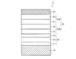
- FIG. 2 is a schematic cross-sectional view showing a configuration of a superconducting thin film material according to Embodiment 1.
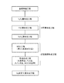
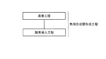
- FIG. It is a figure which shows the outline of the manufacturing process in the manufacturing method of the superconducting thin film material of Embodiment 1. It is a figure which shows the detail of a MOD layer formation process among the manufacturing processes of FIG. It is a figure which shows the detail of a gaseous-phase synthesis process among the manufacturing processes of FIG.
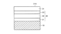
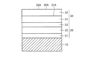
- FIG. 5 is a schematic cross-sectional view for illustrating the method for manufacturing the superconducting thin film material according to the first embodiment.
- FIG. 5 is a schematic cross-sectional view for illustrating the method for manufacturing the superconducting thin film material of the first embodiment.
- FIG. 5 is a schematic cross-sectional view for illustrating the method for manufacturing the superconducting thin film material according to the first embodiment.
- FIG. 5 is a schematic cross-sectional view showing a configuration of a superconducting thin film material in a second embodiment.
- FIG. 10 is a schematic cross-sectional view for illustrating the method for manufacturing the superconducting thin film material of the second embodiment.
- FIG. 10 is a schematic cross-sectional view for illustrating the method for manufacturing the superconducting thin film material of the second embodiment.
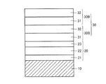
- 6 is a schematic cross-sectional view showing a configuration of a superconducting thin film material in Embodiment 3.
- FIG. It is a figure which shows the outline of the manufacturing process in the manufacturing method of the superconducting thin film material of Embodiment 3.
- FIG. 10 is a schematic cross-sectional view for illustrating the method for manufacturing the superconducting thin film material of the third embodiment.
- FIG. 10 is a schematic cross-sectional view for illustrating the method for manufacturing the superconducting thin film material of the third embodiment.
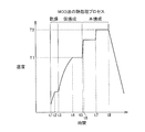
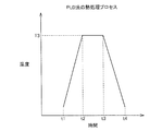
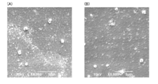
- FIG. 10 is a schematic cross-sectional view for illustrating the method for manufacturing the superconducting thin film material of the third embodiment. It is a graph for demonstrating the process conditions of an example of a MOD method. It is a graph for demonstrating the process conditions of an example of a gaseous-phase method. It is a photograph which shows the experimental result which performed the heat processing on the same conditions as the heat processing in a MOD method with respect to a gaseous-phase synthesis layer. It is a photograph which shows the experimental result which performed the crystallization heat processing on the same conditions as the heat processing in a MOD method with respect to the MOD layer.
- superconducting thin film material 1 of Embodiment 1 includes a metal alignment substrate 10 as a substrate, an intermediate layer 20 formed on metal alignment substrate 10, and a superconductivity formed on intermediate layer 20.
- An oxide superconducting film 30 as a film and an Ag (silver) stabilizing layer 40 as a stabilizing layer formed on the oxide superconducting film 30 to protect the oxide superconducting film 30 are provided.
- Examples of the material of the oxide superconducting film 30 include YBCO (yttrium-based high-temperature superconducting material: YBa 2 Cu 3 O x ), HoBCO (holmium-based high-temperature superconducting material; HoBa 2 Cu 3 O x ), GdBCO (gadolinium-based high-temperature superconducting material). : A rare earth oxide superconducting material such as GdBa 2 Cu 3 O X ) can be selected.
- the oxide superconducting film 30 includes a MOD layer formed by the MOD method and a vapor phase synthesis layer formed on the MOD layer by the vapor phase method.
- the oxide superconducting film 30 includes a MOD-YBCO layer 31 as a MOD layer formed by a MOD method, and a vapor phase synthesis layer formed on the MOD-YBCO layer 31 by a vapor phase method.
- Gas phase synthesis GdBCO layer 32 The oxide superconducting film 30 may be made of the same material for the MOD layer and the vapor phase synthesis layer, but the MOD layer and the vapor phase synthesis layer may be made of different materials.
- a MOD-GdBCO layer instead of the MOD-GdBCO layer may be formed.
- a gas phase synthesis YBCO layer may be formed.
- a Ni (nickel) alignment substrate for example, a Ni alloy-based alignment substrate, or the like can be selected.
- a clad substrate having a laminated structure of Ni / Cu / SUS, a clad substrate having a laminated structure of NiW / SUS, or a NiW substrate can be used.
- the intermediate layer 20 may be a layer containing at least one of Y 2 O 3 (yttria), YSZ (yttria stabilized zirconia) and CeO 2 (ceria), for example.
- the layer can include a Y 2 O 3 layer 21, a YSZ layer 22 formed on the Y 2 O 3 layer 21, and a CeO 2 layer 23 formed on the YSZ layer 22.
- a CeO 2 layer may be formed in place of the Y 2 O 3 layer 21.
- the intermediate layer 20 is not a three-layer structure as described above, but a two-layer structure such as a Y 2 O 3 layer 21 and a CeO 2 layer formed on the Y 2 O 3 layer 21, or a laminate of four or more layers. It is good also as a structure.
- the stabilization layer is not limited to the Ag stabilization layer 40 described above, and for example, a Cu stabilization layer made of Cu (copper) may be used instead of the Ag stabilization layer 40.
- a substrate preparation process is performed. Specifically, a metal alignment substrate 10 such as a tape-shaped substrate made of an oriented nickel alloy is prepared.
- an intermediate layer forming step for forming the intermediate layer 20 on the metal alignment substrate 10 is performed. Specifically, with reference to FIGS. 2 and 5, to sequentially form a Y 2 O 3 layer 21, YSZ layer 22 and CeO 2 layer 23 on the metal textured substrate 10, Y 2 O 3 layer forming step
- the YSZ layer forming step and the CeO 2 layer forming step are sequentially performed.
- the Y 2 O 3 layer forming step, the YSZ layer forming step, and the CeO 2 layer forming step can be performed by a vapor phase method such as a sputtering method, but may be performed by a MOD method.
- a superconducting film forming step for forming an oxide superconducting film 30 on the intermediate layer 20 is performed.
- a MOD step of forming a MOD-YBCO layer 31 on the intermediate layer 20 by the MOD method is performed.
- a coating method of the organometallic salt solution in this fluorine-free solution coating step a dip method, a die coating method, or the like can be selected.
- a drying process for drying the applied solution is performed. Specifically, for example, heat treatment (drying treatment) for removing water and alcohol from the solution applied is performed by setting the drying temperature to 100 ° C. or higher and 150 ° C. or lower.
- the material coated with the solution is placed in a drying furnace and heated.
- the processing apparatus may be configured such that after the tape-shaped metal alignment substrate is passed through the processing unit to which the solution is applied, the metal alignment substrate passes through a drying furnace as it is.
- a temporary firing step is performed in which the solvent component and the like are removed from the applied organometallic salt solution.
- the metal alignment substrate 10 coated with the organometallic salt solution is heated in a temperature range of 400 ° C. to 600 ° C., for example, at 500 ° C.
- the coated organometallic salt solution is heated. Disassembled.
- the solvent component and the like are removed from the applied organic metal salt solution by the separation of CO 2 (carbon dioxide) and H 2 O (water).
- the main firing step is performed.
- the metal alignment substrate 10 coated with the organometallic salt solution is heated in a temperature range of 600 ° C. to 850 ° C., for example, in a mixed atmosphere of Ar (argon) and O 2 (oxygen) at 780 ° C.
- the MOD-YBCO layer 31 which is a MOD layer is formed.
- an oxygen introduction step is performed in which heat treatment for introducing oxygen into the formed MOD-YBCO layer 31 is performed.
- the atmospheric gas is set to 1 atm and 100% O 2 (oxygen)
- the maximum heating temperature is set to 550 ° C.
- cooling is performed to 200 ° C. over 3 hours.
- a vapor phase synthesis step is performed in which a vapor phase synthesized GdBCO layer 32 is formed on the MOD-YBCO layer 31 by a vapor phase method.
- This vapor phase synthesis step preferably uses any thin film forming method selected from the group consisting of a co-evaporation method, a PLD method, a sputtering method, and an MOCVD method.
- the composition of the vapor-phase synthesized GdBCO layer 32 constituting the oxide superconducting film 30 can be made close to the target composition, and high orientation can be ensured. It can contribute to the improvement of Jc and Ic of the material 1.
- a vapor deposition process is first performed.
- the vapor phase synthetic GdBCO layer 32 is formed on the MOD-YBCO layer 31 by using the above-described PLD method or the like.
- an oxygen introduction process is performed. Specifically, in order to introduce oxygen into the formed vapor-phase synthesis GdBCO layer 32, for example, the atmospheric gas is 1 atm and 100% O 2 (oxygen), the maximum heating temperature is 550 ° C., and the temperature is increased to 200 ° C. over 3 hours. To cool.
- the MOD which is the surface of the MOD-YBCO layer 31 even if formed with a certain thickness.
- the surface smoothness of the -YBCO layer surface 31A is kept sufficiently good. Therefore, by forming the gas phase synthetic GdBCO layer 32 on the smooth MOD-YBCO layer surface 31A, the gas phase synthetic GdBCO layer surface 32A, which is the surface of the gas phase synthetic GdBCO layer 32, also has good surface smoothness.
- Such a surface with good surface smoothness is the superconducting film surface 30 ⁇ / b> A which is the surface of the oxide superconducting film 30.
- an oxide superconducting film 30 having excellent surface smoothness is formed, and Ic, Jc and the like of the superconducting thin film material 1 are improved.
- an Ag stabilizing layer forming step is performed in which an Ag stabilizing layer 40 as a stabilizing layer is formed.
- the formation of the Ag stabilizing layer 40 can be performed by, for example, a sputtering method. By performing the above steps, the superconducting thin film material 1 of Embodiment 1 is manufactured.
- the vapor-phase synthesized GdBCO layer 32 is formed.
- 32 is not subjected to heat treatment such as the main firing step of the MOD layer forming step. Therefore, it is possible to suppress the occurrence of a problem that quality such as crystallinity in the vapor-phase synthesized GdBCO layer 32 is deteriorated by the heat treatment. Therefore, as a result, deterioration of the superconducting characteristics of the oxide superconducting film 30 can be suppressed.
- high Jc and high Ic can be obtained by making use of the advantages of both the PLD method and the fluorine-free MOD method while complementing the respective disadvantages.
- the thickness of the MOD-YBCO layer 31 is preferably 1 ⁇ m or less.
- Jc decreases as the film thickness increases. If the MOD-YBCO layer 31 is 1 ⁇ m or less, high Jc is maintained, so that an increase in cost can be suppressed.
- the vapor-phase synthesis GdBCO layer 32 preferably has a thickness of 2 ⁇ m or less, and more preferably 1.5 ⁇ m or less.
- the vapor phase synthetic GdBCO layer 32 formed by the PLD method has a surface smoothness as the film thickness increases, and it becomes difficult to maintain the crystallinity. If the vapor-phase synthesis GdBCO layer 32 is 2 ⁇ m or less, good surface smoothness can be secured relatively easily.
- superconducting thin film material 1 of Embodiment 2 and superconducting thin film material 1 of Embodiment 1 described above basically have the same configuration.
- the first embodiment is that the intermediate layer 20, the oxide superconducting film 30 and the Ag stabilizing layer 40 are formed on both main surfaces of the metal alignment substrate 10. This is different from the superconducting thin film material 1.
- the oxide superconducting film 30 becomes thicker, it becomes difficult to ensure surface smoothness, maintain crystallinity, and suppress high costs due to a decrease in Jc. Become.
- the film thickness of the upper oxide superconducting film 30 can be made equal or thin. As a result, it becomes easy to ensure surface smoothness and maintain crystallinity in the oxide superconducting film 30 on each main surface 10A, and to suppress cost increase due to a decrease in Jc, and the oxide superconducting film on both main surfaces 10A. It is possible to obtain a higher Ic by 30.
- the manufacturing method of the superconducting thin film material of the second embodiment and the manufacturing method of the superconducting thin film material of the first embodiment described with reference to FIGS. 1 to 7 have basically the same configuration.
- the intermediate layer 20, the oxide superconducting film 30, and the Ag stabilizing layer 40 are respectively formed in the intermediate layer forming process, the superconducting film forming process, and the Ag stabilizing layer forming process.
- the second embodiment is different from the first embodiment in that the metal alignment substrate 10 is formed on both main surfaces 10A. Specifically, in the intermediate layer forming step, as shown in FIG.
- oxide superconducting films 30 are formed on both intermediate layers 20 as shown in FIG.
- the Ag stabilizing layer 40 is formed on each of the oxide superconducting films 30 to complete the superconducting thin film material 1 of Embodiment 2 shown in FIG.
- the intermediate layer 20, the oxide superconducting film 30, and the Ag stabilizing layer 40 on both main surfaces 10A of the metal alignment substrate 10 are one side. They may be formed side by side or both at the same time.
- the metal alignment substrate 10 on which the intermediate layer 20 is formed is immersed in an organometallic salt solution by, for example, the dipping method. Can be formed.
- the vapor phase synthesized GdBCO layer 32 When the vapor phase synthesized GdBCO layer 32 is simultaneously formed on both main surfaces 10A by the vapor phase method, the vapor phase synthesized GdBCO layer 32 can be formed from both sides of the metal alignment substrate 10 by the PLD method, for example.
- superconducting thin film material 1 of Embodiment 3 and superconducting thin film material 1 of Embodiment 1 described above have basically the same configuration.
- the superconducting thin film material 1 of Embodiment 3 is different from the oxide superconducting film 30 in that a plurality of structures composed of combinations of the MOD-YBCO layer 31 and the vapor-phase synthesized GdBCO layer 32 are stacked. It is different from the superconducting thin film material 1 of form 1.
- the oxide superconducting film 30 is configured by stacking a plurality of stacked structures 30B each having a vapor-phase synthesized GdBCO layer 32 formed on a MOD-YBCO layer 31.
- FIG. 11 shows a case where the stacked structure 30B is stacked in two stages, the stacked structure 30B may be stacked in three or more stages so that the oxide superconducting film 30 has a desired film thickness.
- the vapor-phase synthesized GdBCO layer 32 formed by the vapor phase method has a surface smoothness as the film thickness increases, and it becomes difficult to maintain the crystallinity. Furthermore, when the vapor-phase synthesized GdBCO layer 32 is formed first and then the MOD-YBCO layer 31 is formed, the quality of the vapor-phase synthesized GdBCO layer 32 is improved by the heat treatment in the main firing step in the formation step of the MOD-YBCO layer 31. There was a case where it deteriorated.
- the vapor-phase synthesized GdBCO layer 32 is formed on the MOD-YBCO layer 31 having excellent crystallinity.
- the quality deterioration of the vapor phase synthesis layer in the structure of Patent Document 1 can be suppressed.
- the quality of the vapor-phase synthesized GdBCO layer 32 can be maintained and the characteristics of the oxide superconducting film 30 can be improved.
- the stacked structure 30B of FIG. It is possible to improve the surface smoothness and the crystallinity of the multilayer structure 30B.
- the MOD-YBCO layer 31 having excellent surface smoothness is formed again on the superconducting film with improved surface smoothness, and the vapor-phase synthetic GdBCO layer 32 is further formed on the MOD-YBCO layer 31. Again, the surface smoothness of the oxide superconducting film 30 is improved.
- the oxide superconducting film 30 can be formed. As a result, it is possible to easily obtain the superconducting thin film material 1 that can ensure desired superconducting properties such as Ic and Jc.
- the method of manufacturing the superconducting thin film material of the third embodiment and the method of manufacturing the superconducting thin film material of the first embodiment described with reference to FIGS. 1 to 7 have basically the same configuration.
- the third embodiment is different from the first embodiment in that in the superconducting film forming step, the MOD step and the gas phase synthesis step are alternately performed a plurality of times.
- an intermediate layer 20 including a Y 2 O 3 layer 21, a YSZ layer 22 and a CeO 2 layer 23 is formed on the metal alignment substrate 10.
- a laminated structure 30 ⁇ / b> B in which a vapor phase synthetic GdBCO layer 32 is formed on the MOD-YBCO layer 31 is formed on the intermediate layer 20.
- the formation method of the MOD-YBCO layer 31 and the vapor-phase synthesis GdBCO layer 32 is the same as that in the first embodiment.
- a laminated structure 30B is further formed on the laminated structure 30B. This laminated structure 30B is repeatedly formed until the oxide superconducting film 30 has a desired film thickness. Then, the Ag stabilizing layer 40 is formed on the oxide superconducting film 30, and the superconducting thin film material 1 of Embodiment 3 shown in FIG. 11 is completed.
- the thickness of the MOD-YBCO layer 31 is preferably 1 ⁇ m or less. If each MOD-YBCO layer 31 is 1 ⁇ m or less, an increase in cost relative to Ic can be suppressed. In the third embodiment, the thickness of each vapor-phase synthesis GdBCO layer 32 is preferably 2 ⁇ m or less, and more preferably 1.5 ⁇ m or less. If each vapor-phase synthesis GdBCO layer 32 is 2 ⁇ m or less, good surface smoothness can be secured relatively easily and crystallinity can be maintained.
- the superconducting thin film material 1 in Embodiments 1 to 3 of the present invention described above is, for example, a tape-shaped wire, but may be in the form of a sheet or a hollow or solid cylindrical shape.
- FIG. 16 shows an example of specific processing conditions (processing temperature pattern) in the MOD layer forming step for forming the MOD-YBCO layer 31 in the first to third embodiments.
- the drying process to the main baking process can be performed with a processing temperature pattern as shown in FIG.
- the horizontal axis of FIG. 16 indicates time
- the vertical axis indicates the processing temperature.
- the drying process is started from time t1, and by heating the substrate from time t1 to time t2, the substrate is heated to a predetermined drying processing temperature at time t2. Then, after the time point t2 when the predetermined drying processing temperature is reached, the temperature is maintained for a certain time (between the time point t2 and the time point t3). In this way, the drying process is performed from time t1 to time t2.
- the time from the time point t1 to the time point t3 can be about 1 hour.
- a temporary baking process is implemented. Specifically, the heating temperature is increased from the time point t3 to the time point t4, and after the heating temperature reaches the temperature T1 (500 ° C.) at the time point t4, the temperature is maintained for a certain time (between the time point t4 and the time point t5). .
- the holding time is about 60 minutes, for example.
- the time from the time point t3 to the time point t5 temporary firing step time
- the heating temperature is further increased from time t5 in FIG. 16, and when the ambient temperature reaches the intermediate heat treatment temperature (about 680 ° C.) at time t6, the temperature is kept for a certain time (between time t6 and time t7). Hold.
- the holding time can be about 90 minutes, for example.
- a temperature range of about 620 ° C. or higher and 750 ° C. or lower can be adopted as the intermediate heat treatment temperature.
- concentration can be 10 ppm or less.
- This intermediate heat treatment is intended to decompose the carbonate in the material to be treated.
- the heating temperature is further increased from time t7, the ambient temperature is increased to the main baking temperature T2 (about 800 ° C.), and the state is maintained for a certain time until time t8. This holding time is about 90 minutes, for example. Thereafter, the ambient temperature is lowered. Then, as an oxygen introduction step, the atmosphere is set to 1 atm and 100% O 2 (oxygen), the maximum heating temperature is set to 550 ° C., and cooling is performed to 200 ° C. over 3 hours, thereby introducing oxygen into the superconducting layer. As a result, the MOD-YBCO layer 31 (see FIG. 1) can be formed.
- the time for the main firing step (time point t5 to time point t8) can be set to about 3 hours, for example.
- a processing temperature pattern as shown in FIG. 17 can be adopted.
- the horizontal axis indicates time
- the vertical axis indicates the processing temperature.
- heating of the substrate temperature is started from time t1, and the heat treatment is continued until time t2 when the substrate temperature reaches temperature T3 (for example, about 700 ° C.). To do.
- T3 for example, about 700 ° C.
- a vapor phase synthetic GdBCO layer is formed on the previously formed MOD-YBCO layer by the PLD method. While the vapor phase synthetic GdBCO layer is formed by the PLD method (between time t2 and time t3 in FIG. 17), the temperature of the substrate is maintained at a temperature T3 (for example, about 700 ° C.).
- the film formation time using this PLD method (between time t2 and time t3) is, for example, about several minutes. Thereafter, the substrate temperature is lowered from time t3, and the substrate is cooled to time t4 when the temperature reaches a predetermined temperature. Thereafter, as an oxygen introduction step, the atmosphere is set to 1 atm and 100% O 2 (oxygen), the maximum heating temperature is set to 550 ° C., and cooling is performed to 200 ° C. over 3 hours, thereby introducing oxygen into the superconducting layer. As a result, the vapor-phase synthesis GdBCO layer 32 (see FIG. 1) can be formed.
- O 2 oxygen
- Example 1 In order to confirm the effect of the present invention, the following experiment was conducted.
- sample In order to investigate the influence of the heat treatment by the MOD method on the MOD layer and the vapor phase synthesis layer, the following samples were prepared. That is, a sample (sample No. 1) in which an intermediate layer is formed on the substrate and a vapor-phase synthesis GdBCO layer is formed on the intermediate layer, an intermediate layer is formed on the substrate, and the MOD- A sample (sample No. 2) on which a YBCO layer was formed was prepared.
- Example No. 1 A substrate made of an oriented nickel alloy (NiW) was used as the substrate. Then, as the intermediate layer, Y 2 O 3 layer on the substrate by sputtering were sequentially formed a YSZ layer and CeO 2 layer. Regarding the thicknesses of these layers, the Y 2 O 3 layer has a thickness of 0.12 ⁇ m, the YSZ layer has a thickness of 0.44 ⁇ m, and the CeO 2 layer has a thickness of 0.06 ⁇ m. Further, a gas phase synthetic GdBCO layer having a thickness of about 1.5 ⁇ m was formed on the intermediate layer by using the PLD method. The film forming temperature was about 700 ° C.
- Example No. 2 Sample No. above.
- a substrate similar to that of Sample No. 1 was prepared.
- an intermediate layer was formed on the substrate.
- a MOD-YBCO layer having a thickness of about 1.5 ⁇ m was formed on the intermediate layer by using the MOD method.
- the drying process to the main firing process were performed on the substrate coated with the solution with a processing temperature pattern as shown in FIG. Referring to FIG. 16, the time for the drying process (the time from time t1 to time t3 in FIG. 16) was about 1 hour.
- the temporary baking process was implemented as shown in FIG. Specifically, the temperature T1, which is the heating temperature at time t4 in FIG. 16, was set to 500 ° C., and the temperature was maintained for a certain period of time (about 60 minutes from time t4 to time t5). Further, the time from the time point t3 to the time point t5 (temporary firing step time) was about 3 hours.
- the heating temperature is further increased from time t5 in FIG. 16, and when the ambient temperature reaches the intermediate heat treatment temperature (about 680 ° C.) at time t6, the temperature is set for a certain period of time (from time t6 to time t7). For about 90 minutes). Moreover, about the atmosphere at this time, the carbon dioxide concentration was 10 ppm or less.
- the heating temperature was further increased from time t7, the ambient temperature was raised to the main firing temperature T2 (about 800 ° C.), and the state was maintained for a certain time (about 90 minutes) until time t8. Thereafter, the ambient temperature was lowered. In this way, a MOD-YBCO layer was formed.
- FIG. 18A shows a sample No. 1 in which a gas phase synthetic GdBCO layer (PLD film) is formed.
- 1 shows the surface of the gas phase synthesized GdBCO layer before the above-described heat treatment is performed (the state in which the gas phase synthesized GdBCO layer is still formed).
- FIG. 18B shows the surface of the vapor-phase synthesis GdBCO layer after the heat treatment is performed.
- the vapor phase synthetic GdBCO layer which is a PLD film, has a different phase formed on the surface by the heat treatment.
- FIG. 19A shows a sample No. with a MOD-YBCO layer formed. 2 shows the surface of the MOD-YBCO layer before the heat treatment described above is performed (the state in which the MOD-YBCO layer is still formed).
- FIG. 19B shows the surface of the MOD-YBCO layer after the above heat treatment is performed. As can be seen from FIG. 19, in the MOD-YBCO layer, there is no significant change in the surface state due to the heat treatment.
- the superconducting thin film material and the manufacturing method thereof according to the present invention can be particularly advantageously applied to a superconducting thin film material in which a superconducting film is formed on a substrate and a manufacturing method thereof.
Landscapes
- Engineering & Computer Science (AREA)
- Manufacturing & Machinery (AREA)
- Chemical & Material Sciences (AREA)
- Ceramic Engineering (AREA)
- Superconductors And Manufacturing Methods Therefor (AREA)
Abstract
Description
図1を参照して、実施の形態1の超電導薄膜材料の構成について説明する。
図8を参照して実施の形態2の超電導薄膜材料の構成を説明する。
図11を参照して、本発明の実施の形態3の超電導薄膜材料の構成を説明する。
本発明の効果を確認するべく、以下のような実験を実施した。
MOD層と気相合成層とに対する、MOD法での熱処理の影響を調査するべく、以下のような試料を準備した。すなわち、基板上に中間層が形成され、当該中間層上に気相合成GdBCO層が形成された試料(試料No.1)と、基板上に中間層が形成され、当該中間層上にMOD-YBCO層が形成された試料(試料No.2)とを準備した。
基板としては配向性のニッケル合金(NiW)からなる基板を用いた。そして、中間層としては、スパッタリング法を用いて基板上にY2O3層、YSZ層およびCeO2層を順次形成した。これらの各層の厚みについて、Y2O3層の厚みが0.12μm、YSZ層の厚みが0.44μm、CeO2層の厚みが0.06μmである。さらに、当該中間層上にPLD法を用いて厚みが約1.5μmの気相合成GdBCO層を形成した。成膜温度は約700℃とした。
上記試料No.1と同様の基板を準備し、上記試料No.1と同様に中間層を当該基板上に形成した。そして、中間層上に、MOD法を用いて厚みが約1.5μmのMOD-YBCO層を形成した。なお、用いた有機金属塩溶液は実施の形態1において説明した金属アセチルアセトナト系の溶液(Y:Ba:Cu=1:2:3)を用いた。
上記試料No.1および試料No.2のそれぞれについて、図16に示したMOD法の熱処理を再度加えて、当該熱処理前後についてその表面状態を走査型電子顕微鏡により観察した。
測定結果を図18および図19に示す。図18(A)には、気相合成GdBCO層(PLD膜)が形成された試料No.1の表面について、上述した熱処理が実施される前(気相合成GdBCO層が形成されたままの状態)の、気相合成GdBCO層の表面が示されている。そして、図18(B)では、上記熱処理が実施された後の、気相合成GdBCO層の表面が示されている。図18から分かるように、PLD膜である気相合成GdBCO層は、当該熱処理によって表面に異相が形成されている。
Claims (8)
- 基板(10)と、
前記基板(10)上に形成された超電導膜(30)とを備え、
前記超電導膜(30)は、
MOD法により形成されたMOD層(31)と、
前記MOD層(31)上に気相法により形成された気相合成層(32)とを含んでいる、超電導薄膜材料。 - 前記基板(10)と前記超電導膜(30)との間に、さらに中間層(20)を備えた、請求項1に記載の超電導薄膜材料。
- 前記超電導膜(30)は、前記基板(10)の両方の主面上に形成されている、請求項1または2に記載の超電導薄膜材料。
- 前記超電導膜(30)においては、前記MOD層(31)と、前記気相合成層(32)との組み合わせからなる構造が複数積層されている、請求項1~3のいずれか1項に記載の超電導薄膜材料。
- 前記MOD層(31)の厚みは1μm以下である、請求項1~4のいずれか1項に記載の超電導薄膜材料。
- 前記気相合成層(32)の厚みは2μm以下である、請求項1~5のいずれか1項に記載の超電導薄膜材料。
- 前記MOD法は、フッ素を含む有機金属塩溶液を使用しない無フッ素系MOD法である、請求項1~6のいずれか1項に記載の超電導薄膜材料。
- 基板(10)を準備する工程と、
前記基板(10)上に超電導膜(30)を形成する工程とを備え、
前記超電導膜(30)を形成する工程は、
MOD法によりMOD層(31)を形成する工程と、
前記MOD層(31)上に気相法により気相合成層(32)を形成する工程とを含んでいる、超電導薄膜材料の製造方法。
Priority Applications (3)
| Application Number | Priority Date | Filing Date | Title |
|---|---|---|---|
| US14/112,086 US9082530B2 (en) | 2011-05-30 | 2012-05-09 | Superconducting thin film material and method of manufacturing same |
| CN201280024544.0A CN103548100B (zh) | 2011-05-30 | 2012-05-09 | 超导薄膜材料和其制造方法 |
| DE112012002313.7T DE112012002313T5 (de) | 2011-05-30 | 2012-05-09 | Supraleitendes Dünnfilmmaterial und Verfahren zu seiner Herstellung |
Applications Claiming Priority (2)
| Application Number | Priority Date | Filing Date | Title |
|---|---|---|---|
| JP2011-120500 | 2011-05-30 | ||
| JP2011120500A JP5838596B2 (ja) | 2011-05-30 | 2011-05-30 | 超電導薄膜材料およびその製造方法 |
Publications (1)
| Publication Number | Publication Date |
|---|---|
| WO2012165109A1 true WO2012165109A1 (ja) | 2012-12-06 |
Family
ID=47258973
Family Applications (1)
| Application Number | Title | Priority Date | Filing Date |
|---|---|---|---|
| PCT/JP2012/061843 Ceased WO2012165109A1 (ja) | 2011-05-30 | 2012-05-09 | 超電導薄膜材料およびその製造方法 |
Country Status (6)
| Country | Link |
|---|---|
| US (1) | US9082530B2 (ja) |
| JP (1) | JP5838596B2 (ja) |
| CN (1) | CN103548100B (ja) |
| DE (1) | DE112012002313T5 (ja) |
| TW (1) | TW201316576A (ja) |
| WO (1) | WO2012165109A1 (ja) |
Cited By (2)
| Publication number | Priority date | Publication date | Assignee | Title |
|---|---|---|---|---|
| US20160163424A1 (en) * | 2013-11-12 | 2016-06-09 | Varian Semiconductor Equipment Associated, Inc. | Integrated superconductor device and method of fabrication |
| US9947441B2 (en) | 2013-11-12 | 2018-04-17 | Varian Semiconductor Equipment Associates, Inc. | Integrated superconductor device and method of fabrication |
Families Citing this family (7)
| Publication number | Priority date | Publication date | Assignee | Title |
|---|---|---|---|---|
| WO2014008384A1 (en) * | 2012-07-05 | 2014-01-09 | University Of Houston System | Superconducting article with compliant layers |
| WO2016076451A1 (ko) * | 2014-11-11 | 2016-05-19 | 엘에스전선 주식회사 | 초전도 케이블 |
| JP6861633B2 (ja) | 2015-10-15 | 2021-04-21 | 住友電気工業株式会社 | 酸化物超電導線材 |
| CN108352227A (zh) * | 2015-11-05 | 2018-07-31 | 住友电气工业株式会社 | 薄膜氧化物超导线材及其制造方法 |
| CN107978394A (zh) * | 2016-10-25 | 2018-05-01 | 上海新昇半导体科技有限公司 | 超导带及其制造方法 |
| US11380463B2 (en) * | 2017-02-14 | 2022-07-05 | Sumitomo Electric Industries, Ltd. | Superconducting wire and superconducting coil |
| KR102453489B1 (ko) * | 2018-04-10 | 2022-10-11 | 한국전기연구원 | 초전도층이 적층된 고온초전도선재 및 그 제조방법 |
Citations (2)
| Publication number | Priority date | Publication date | Assignee | Title |
|---|---|---|---|---|
| JP2007220467A (ja) * | 2006-02-16 | 2007-08-30 | Sumitomo Electric Ind Ltd | 超電導薄膜材料の製造方法、超電導機器、および超電導薄膜材料 |
| JP2007311234A (ja) * | 2006-05-19 | 2007-11-29 | Sumitomo Electric Ind Ltd | 超電導薄膜材料およびその製造方法 |
Family Cites Families (5)
| Publication number | Priority date | Publication date | Assignee | Title |
|---|---|---|---|---|
| US5449659A (en) * | 1991-07-05 | 1995-09-12 | Conductus, Inc. | Method of bonding multilayer structures of crystalline materials |
| JP4433589B2 (ja) | 2000-08-29 | 2010-03-17 | 住友電気工業株式会社 | 高温超電導厚膜部材およびその製造方法 |
| JP2006216365A (ja) * | 2005-02-03 | 2006-08-17 | Sumitomo Electric Ind Ltd | 超電導薄膜材料、超電導線材およびこれらの製造方法 |
| WO2007094147A1 (ja) * | 2006-02-16 | 2007-08-23 | Sumitomo Electric Industries, Ltd. | 超電導薄膜材料の製造方法、超電導機器、および超電導薄膜材料 |
| JP2010257844A (ja) * | 2009-04-27 | 2010-11-11 | Sumitomo Electric Ind Ltd | 酸化物超電導線材の製造装置 |
-
2011
- 2011-05-30 JP JP2011120500A patent/JP5838596B2/ja active Active
-
2012
- 2012-05-09 US US14/112,086 patent/US9082530B2/en active Active
- 2012-05-09 WO PCT/JP2012/061843 patent/WO2012165109A1/ja not_active Ceased
- 2012-05-09 CN CN201280024544.0A patent/CN103548100B/zh active Active
- 2012-05-09 DE DE112012002313.7T patent/DE112012002313T5/de not_active Withdrawn
- 2012-05-24 TW TW101118517A patent/TW201316576A/zh unknown
Patent Citations (2)
| Publication number | Priority date | Publication date | Assignee | Title |
|---|---|---|---|---|
| JP2007220467A (ja) * | 2006-02-16 | 2007-08-30 | Sumitomo Electric Ind Ltd | 超電導薄膜材料の製造方法、超電導機器、および超電導薄膜材料 |
| JP2007311234A (ja) * | 2006-05-19 | 2007-11-29 | Sumitomo Electric Ind Ltd | 超電導薄膜材料およびその製造方法 |
Cited By (4)
| Publication number | Priority date | Publication date | Assignee | Title |
|---|---|---|---|---|
| US20160163424A1 (en) * | 2013-11-12 | 2016-06-09 | Varian Semiconductor Equipment Associated, Inc. | Integrated superconductor device and method of fabrication |
| US9947441B2 (en) | 2013-11-12 | 2018-04-17 | Varian Semiconductor Equipment Associates, Inc. | Integrated superconductor device and method of fabrication |
| US10158061B2 (en) * | 2013-11-12 | 2018-12-18 | Varian Semiconductor Equipment Associates, Inc | Integrated superconductor device and method of fabrication |
| US10290399B2 (en) | 2013-11-12 | 2019-05-14 | Varian Semiconductor Equipment Associates, Inc. | Integrated superconductor device and method of fabrication |
Also Published As
| Publication number | Publication date |
|---|---|
| US20140038829A1 (en) | 2014-02-06 |
| DE112012002313T5 (de) | 2014-03-20 |
| CN103548100A (zh) | 2014-01-29 |
| TW201316576A (zh) | 2013-04-16 |
| CN103548100B (zh) | 2016-04-20 |
| JP2012248469A (ja) | 2012-12-13 |
| US9082530B2 (en) | 2015-07-14 |
| JP5838596B2 (ja) | 2016-01-06 |
Similar Documents
| Publication | Publication Date | Title |
|---|---|---|
| JP5838596B2 (ja) | 超電導薄膜材料およびその製造方法 | |
| RU2384907C1 (ru) | Сверхпроводящий тонкопленочный материал и способ его изготовления | |
| JP5156188B2 (ja) | 厚膜テープ状re系(123)超電導体の製造方法 | |
| JP2007165153A6 (ja) | 厚膜テープ状re系(123)超電導体の製造方法。 | |
| JP2003300726A (ja) | テープ状酸化物超電導体及びその製造方法 | |
| JP2005001935A (ja) | 酸化物薄膜の製造方法 | |
| JP5415824B2 (ja) | 被覆された導体のための、形状を変化させた基板の製造方法及び上記基板を使用する被覆された導体 | |
| JP2013235765A (ja) | 酸化物超電導線材とその製造方法 | |
| JP2011253766A (ja) | 酸化物超電導薄膜の製造方法 | |
| JP2011253768A (ja) | 酸化物超電導薄膜の製造方法 | |
| JP2012064394A (ja) | 酸化物超電導薄膜の製造方法 | |
| JP5591900B2 (ja) | 厚膜テープ状re系(123)超電導体の製造方法 | |
| KR100998310B1 (ko) | 유기금속증착용 전구용액 형성방법 및 이를 사용하는초전도 후막 형성방법 | |
| JP2011096593A (ja) | 酸化物超電導薄膜の製造方法 | |
| JP5556410B2 (ja) | 酸化物超電導薄膜の製造方法 | |
| JP2012003962A (ja) | 酸化物超電導薄膜の製造方法 | |
| WO2013153651A1 (ja) | 酸化物超電導薄膜線材とその製造方法 | |
| JP2011230946A (ja) | 酸化物超電導薄膜の製造方法 | |
| JP2012129085A (ja) | 酸化物超電導薄膜線材とその製造方法 | |
| JP2012123998A (ja) | 酸化物超電導薄膜線材とその製造方法 | |
| JP2013218799A (ja) | 酸化物超電導線材とその製造方法 | |
| JP2012174567A (ja) | 酸化物超電導線材とその製造方法 | |
| JP2012113860A (ja) | 酸化物超電導薄膜線材とその製造方法 | |
| JP2010238633A (ja) | 希土類系厚膜酸化物超電導線材の製造方法 | |
| JP2012018799A (ja) | 酸化物超電導薄膜の製造方法 |
Legal Events
| Date | Code | Title | Description |
|---|---|---|---|
| WWE | Wipo information: entry into national phase |
Ref document number: 201280024544.0 Country of ref document: CN |
|
| 121 | Ep: the epo has been informed by wipo that ep was designated in this application |
Ref document number: 12793725 Country of ref document: EP Kind code of ref document: A1 |
|
| WWE | Wipo information: entry into national phase |
Ref document number: 14112086 Country of ref document: US |
|
| WWE | Wipo information: entry into national phase |
Ref document number: 112012002313 Country of ref document: DE Ref document number: 1120120023137 Country of ref document: DE |
|
| 122 | Ep: pct application non-entry in european phase |
Ref document number: 12793725 Country of ref document: EP Kind code of ref document: A1 |