WO2012165082A1 - 圧力センサ及びその製造方法並びに圧力検出モジュール - Google Patents
圧力センサ及びその製造方法並びに圧力検出モジュール Download PDFInfo
- Publication number
- WO2012165082A1 WO2012165082A1 PCT/JP2012/060738 JP2012060738W WO2012165082A1 WO 2012165082 A1 WO2012165082 A1 WO 2012165082A1 JP 2012060738 W JP2012060738 W JP 2012060738W WO 2012165082 A1 WO2012165082 A1 WO 2012165082A1
- Authority
- WO
- WIPO (PCT)
- Prior art keywords
- pressure
- cover
- pressure sensor
- electrode
- film
- Prior art date
- Legal status (The legal status is an assumption and is not a legal conclusion. Google has not performed a legal analysis and makes no representation as to the accuracy of the status listed.)
- Ceased
Links
Images




Classifications
-
- G—PHYSICS
- G01—MEASURING; TESTING
- G01L—MEASURING FORCE, STRESS, TORQUE, WORK, MECHANICAL POWER, MECHANICAL EFFICIENCY, OR FLUID PRESSURE
- G01L1/00—Measuring force or stress, in general
- G01L1/20—Measuring force or stress, in general by measuring variations in ohmic resistance of solid materials or of electrically-conductive fluids; by making use of electrokinetic cells, i.e. liquid-containing cells wherein an electrical potential is produced or varied upon the application of stress
- G01L1/205—Measuring force or stress, in general by measuring variations in ohmic resistance of solid materials or of electrically-conductive fluids; by making use of electrokinetic cells, i.e. liquid-containing cells wherein an electrical potential is produced or varied upon the application of stress using distributed sensing elements
-
- G—PHYSICS
- G01—MEASURING; TESTING
- G01L—MEASURING FORCE, STRESS, TORQUE, WORK, MECHANICAL POWER, MECHANICAL EFFICIENCY, OR FLUID PRESSURE
- G01L1/00—Measuring force or stress, in general
- G01L1/20—Measuring force or stress, in general by measuring variations in ohmic resistance of solid materials or of electrically-conductive fluids; by making use of electrokinetic cells, i.e. liquid-containing cells wherein an electrical potential is produced or varied upon the application of stress
-
- G—PHYSICS
- G01—MEASURING; TESTING
- G01L—MEASURING FORCE, STRESS, TORQUE, WORK, MECHANICAL POWER, MECHANICAL EFFICIENCY, OR FLUID PRESSURE
- G01L5/00—Apparatus for, or methods of, measuring force, work, mechanical power, or torque, specially adapted for specific purposes
- G01L5/22—Apparatus for, or methods of, measuring force, work, mechanical power, or torque, specially adapted for specific purposes for measuring the force applied to control members, e.g. control members of vehicles, triggers
- G01L5/226—Apparatus for, or methods of, measuring force, work, mechanical power, or torque, specially adapted for specific purposes for measuring the force applied to control members, e.g. control members of vehicles, triggers to manipulators, e.g. the force due to gripping
- G01L5/228—Apparatus for, or methods of, measuring force, work, mechanical power, or torque, specially adapted for specific purposes for measuring the force applied to control members, e.g. control members of vehicles, triggers to manipulators, e.g. the force due to gripping using tactile array force sensors
-
- A—HUMAN NECESSITIES
- A61—MEDICAL OR VETERINARY SCIENCE; HYGIENE
- A61B—DIAGNOSIS; SURGERY; IDENTIFICATION
- A61B2562/00—Details of sensors; Constructional details of sensor housings or probes; Accessories for sensors
- A61B2562/02—Details of sensors specially adapted for in-vivo measurements
- A61B2562/0247—Pressure sensors
-
- A—HUMAN NECESSITIES
- A61—MEDICAL OR VETERINARY SCIENCE; HYGIENE
- A61B—DIAGNOSIS; SURGERY; IDENTIFICATION
- A61B5/00—Measuring for diagnostic purposes; Identification of persons
- A61B5/103—Measuring devices for testing the shape, pattern, colour, size or movement of the body or parts thereof, for diagnostic purposes
- A61B5/1036—Measuring load distribution, e.g. podologic studies
-
- A—HUMAN NECESSITIES
- A61—MEDICAL OR VETERINARY SCIENCE; HYGIENE
- A61B—DIAGNOSIS; SURGERY; IDENTIFICATION
- A61B5/00—Measuring for diagnostic purposes; Identification of persons
- A61B5/68—Arrangements of detecting, measuring or recording means, e.g. sensors, in relation to patient
- A61B5/6801—Arrangements of detecting, measuring or recording means, e.g. sensors, in relation to patient specially adapted to be attached to or worn on the body surface
- A61B5/6802—Sensor mounted on worn items
- A61B5/6804—Garments; Clothes
- A61B5/6806—Gloves
-
- G—PHYSICS
- G06—COMPUTING OR CALCULATING; COUNTING
- G06F—ELECTRIC DIGITAL DATA PROCESSING
- G06F3/00—Input arrangements for transferring data to be processed into a form capable of being handled by the computer; Output arrangements for transferring data from processing unit to output unit, e.g. interface arrangements
- G06F3/01—Input arrangements or combined input and output arrangements for interaction between user and computer
- G06F3/03—Arrangements for converting the position or the displacement of a member into a coded form
- G06F3/041—Digitisers, e.g. for touch screens or touch pads, characterised by the transducing means
- G06F3/0416—Control or interface arrangements specially adapted for digitisers
-
- G—PHYSICS
- G06—COMPUTING OR CALCULATING; COUNTING
- G06F—ELECTRIC DIGITAL DATA PROCESSING
- G06F3/00—Input arrangements for transferring data to be processed into a form capable of being handled by the computer; Output arrangements for transferring data from processing unit to output unit, e.g. interface arrangements
- G06F3/01—Input arrangements or combined input and output arrangements for interaction between user and computer
- G06F3/03—Arrangements for converting the position or the displacement of a member into a coded form
- G06F3/041—Digitisers, e.g. for touch screens or touch pads, characterised by the transducing means
- G06F3/044—Digitisers, e.g. for touch screens or touch pads, characterised by the transducing means by capacitive means
-
- G—PHYSICS
- G06—COMPUTING OR CALCULATING; COUNTING
- G06F—ELECTRIC DIGITAL DATA PROCESSING
- G06F3/00—Input arrangements for transferring data to be processed into a form capable of being handled by the computer; Output arrangements for transferring data from processing unit to output unit, e.g. interface arrangements
- G06F3/01—Input arrangements or combined input and output arrangements for interaction between user and computer
- G06F3/03—Arrangements for converting the position or the displacement of a member into a coded form
- G06F3/041—Digitisers, e.g. for touch screens or touch pads, characterised by the transducing means
- G06F3/045—Digitisers, e.g. for touch screens or touch pads, characterised by the transducing means using resistive elements, e.g. a single continuous surface or two parallel surfaces put in contact
Definitions
- the present invention relates to a pressure sensor that can be integrally formed on a flexible circuit board and is suitable for measurement of pressure distribution used for a flexible curved surface including a spherical curved surface, a manufacturing method thereof, and a pressure detection module.
- a general pressure distribution sensor on the market is basically composed of a rectangular thin sheet. Since it is a sheet shape, measurement on a cylindrical curved surface is possible, but it is not suitable for measurement on a flexible curved surface including a spherical curved surface. This is related to the wire-saving technology (matrix wiring) that collects (N + M) pressure points at (N x M) points, and because the wiring is vertical and horizontal, the shape of the measurement area is restricted to a square shape, etc. It is to be done.
- These pressure distribution sensors are mainly mounted with PET film and printed wiring, but the wiring density is low due to the printing accuracy and migration of the wiring, and the wiring is not flexible and bend-bending resistant. There is no. Furthermore, since it is not suitable for solder reflow, it is difficult to mount components, and there is a problem that it must be connected to a signal processing device with a large connector.
- a tactile sensor capable of measuring pressure distribution on various curved surfaces is made of a tree-like substrate with a band-like part, and can be converted to analog-digital conversion and communication instead of matrix wiring.
- a technology based on IC-type wiring saving in which a small IC or the like is mounted on a sensor sheet has been proposed (see Patent Document 1).
- the pressure detection unit and the wiring are laid along the belt-like portion, so that the space is small and high-density wiring is necessary.
- electronic components are placed on the substrate for IC-type wiring saving. Must be implemented directly. For this reason, the pressure detection is not a method using a general PET film and printed wiring as described above, but a flexible circuit board used in a general electronic device is suitable.
- Patent Document 1 the configuration of the pressure sensor applied to the pressure detection unit is arbitrary.
- the existing pressure sensor has a problem that a measurement error occurs, flexibility cannot be increased, and miniaturization is difficult.
- a pressure detection mechanism used for a general pressure distribution sensor has a mainstream structure in which a pressure sensitive resistance material or an elastic dielectric is sandwiched between two films (for example, FlexiForce (product of NITTA Corporation) Name) and Tekscan (product name).
- FlexiForce product of NITTA Corporation
- Tekscan product name
- an extension force is generated along the film surface during bending, which may cause an error.
- bending especially when the curvature changes dynamically, it is very difficult to distinguish between this internal pressure and the external pressure that is originally intended to be measured, which is a major error factor in pressure distribution measurement on a flexible curved surface.
- a sensor using matrix wiring or a capacitance method in which an elastic dielectric is sandwiched requires electrodes and wiring on upper and lower films, so that there is a problem that the sensor becomes thick and flexibility is deteriorated. This means that an external force is required for the bending of the sensor itself, and it becomes an error with respect to the external force to be originally measured.
- general pressure-sensitive resistors are mainly composed of conductive powder dispersed in a binder such as rubber, but these cannot be said to have high heat resistance.
- a binder such as rubber
- a certain heat resistance is also required, so the material needs attention.
- the present invention has been made to solve the above-described problems of the prior art, and the object of the present invention is that it can be molded with the components of a flexible circuit board, and has a low measurement error during bending and high flexibility.
- Another object of the present invention is to provide a pressure sensor that is excellent in compactness, high density, heat resistance, and the like, a manufacturing method thereof, and a pressure detection module.
- the pressure sensor of the present invention comprises: A base film provided with a conductor pattern having one or more electrodes; A cover film laminated on a base film so as to cover the electrode of the conductor pattern; A spacer that is provided between the cover film and the base film, and that forms a hollow portion having a predetermined gap between the electrode and the cover film,
- the portion of the cover film corresponding to the hollow portion has a pressure-sensitive portion that can be deformed in a direction contacting and separating from the electrode according to pressure, and a contact resistance changes according to the contact pressure with the electrode, It is the structure which detects a pressure by the change of contact resistance.
- the conductor pattern including the electrode is only the base film, the thickness is thin, flexible and flexible, the external force required for the bending itself is small, and the measurement error can be further reduced. Since the conductor pattern including the electrodes can be formed in the same manner as the wiring layer of a normal flexible circuit board, the wiring pattern can be made small and the wiring density can be increased. Furthermore, since the contact resistance method is used, it has high heat resistance and is suitable for a reflow process necessary for IC type wiring saving.
- the electrodes may be configured as a pair of electrodes arranged side by side on the base film, or may be configured to be one in the base film and electrically connected to the pressure sensitive part.
- the base film has a belt-like configuration and the hollow portion is open to one side edge of the base film, the flexibility becomes higher and the measurement error can be reduced. If a metal conductor such as gold plating for preventing oxidation is plated on the exposed portion of the conductor pattern, the deterioration of the electrode due to oxidation can be prevented. In addition, a plating mask is required for plating, but since the portion covered with the spacer such as the photosensitive cover cannot be plated, it is completely formed of copper foil or the like by the photosensitive cover and metal plating. The conductor pattern can be protected.
- the cover film is provided with a notch for reducing the tensile force at the time of bending, the generation of internal pressure at the time of bending can be further reduced, and the measurement error can be further reduced.
- the pressure-sensitive part is a pressure-sensitive thin film formed on a cover film, it can be laminated in the production line of a general flexible circuit board, so special mounting processes can be reduced and cost reduction can be realized.
- the spacer or / and the bank is composed of a photosensitive cover, it can be processed into a fine shape by exposure / development using a mask. The bank can be formed with high accuracy. Providing protrusions on the cover film makes it easier for the cover film to be pushed into the hollow area, resulting in an increase in initial sensitivity.
- the manufacturing method of the pressure sensor of the present invention forms a conductor pattern including a pair of electrodes on a base film, Laminating a photosensitive cover on the base film, removing at least a portion corresponding to the pair of electrodes of the conductor pattern, exposing the remaining portion of the conductor pattern with the remaining portion of the photosensitive cover, The exposed portion including the pair of electrodes of the conductor pattern is subjected to an anti-oxidation metal plating treatment, Thereafter, a cover film in which a pressure-sensitive portion whose contact resistance changes depending on the contact pressure with the electrode is laminated in advance, and the photosensitive cover is attached to the remaining portion of the photosensitive cover with an adhesive. A hollow portion is formed in a portion corresponding to the removed pair of electrodes.
- a photosensitive cover When removing the part corresponding to the pair of electrodes of the photosensitive cover, a photosensitive cover is used to form a bank that prevents the adhesive from flowing into the hollow part in front of the hollow part. Is characterized in that the cover film is non-adhesive.
- Another manufacturing method forms a conductor pattern with one electrode on a base film, Laminating a photosensitive cover on the base film, exposing at least a portion corresponding to the electrode of the conductor pattern, and covering the remaining portion of the conductor pattern with the remaining portion of the photosensitive cover;
- the exposed portion including the electrode of the conductor pattern is subjected to an anti-oxidation metal plating treatment, Thereafter, a pressure-sensitive portion whose contact resistance is changed by contact pressure with the electrode and a cover film in which an electrode electrically connected to the pressure-sensitive portion is formed in advance are laminated, and bonded to the remaining portion of the photosensitive cover
- a hollow portion is formed in a portion corresponding to the electrode removed from the photosensitive cover.
- the photosensitive cover when removing the portion of the photosensitive cover corresponding to the electrode on the base film, the photosensitive cover is used, and the adhesive to the hollow portion is placed before the hollow portion. It is preferable that a bank for preventing inflow is formed, and the cover film is not bonded to the bank.
- the pressure detection module of the present invention includes a flexible circuit board having one or a plurality of strip-shaped portions, and the above-described pressure sensor arranged in one or a plurality of strip-shaped portions constituting the flexible circuit board. It has a configuration.
- the pressure sensor can be brought into close contact with a three-dimensional shape such as a spherical curved surface, and the pressure distribution can be detected accurately.
- the detection portions of the pressure sensor can be arranged with higher density.
- the flexible circuit board is electrically connected to the pressure sensor and the communication terminal by one or more communication terminals and wiring provided on the flexible circuit board, and receives information acquired by each pressure sensor. And it can also be set as the structure provided with the 1 or more electronic circuit part which has a communication function which transmits the said information to the terminal for communication.
- the hollow portion is formed, high flexibility is obtained, the influence of bending is small, and the measurement error can be reduced.
- the conductor pattern can achieve high density as with the wiring layer of the conventional flexible circuit board, and can be downsized. Furthermore, since contact resistance is used, it has excellent heat resistance and can be applied to solder reflow and the like. Moreover, since it is comprised with the material used for a flexible circuit board, it can manufacture easily with the manufacturing equipment of the conventional flexible circuit board.
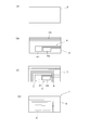
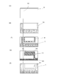
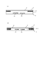
- FIG. 1 A schematic exploded perspective view of the state which removed the film cover and exposed the hollow part
- C is a schematic sectional view exaggerating the thickness of each part.
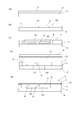
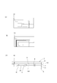
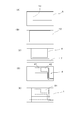
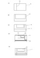
- or (D) is a top view which decomposes
- or (E) is sectional drawing which decomposes
- FIG. 1A is a schematic cross-sectional view showing an example in which an end surface of an adhesive sheet is retracted from a photosensitive cover as a spacer
- FIG. It is a schematic sectional drawing which shows the example used only as.
- the pressure sensor of the present invention has a structure in which a detection principle based on a contact resistance method is introduced and directly embedded in a flexible circuit board.
- the pressure sensor is constructed from general-purpose flexible circuit board materials such as base film, film cover, and photosensitive cover (PSC), so that the pressure inside the flexible circuit board A structure for embedding the sensor is realized.
- This pressure sensor is not only suitable for high density because the pressure detection part can be made compact by preventing the adhesive from flowing into the electrode by the bank, but also suppresses the internal pressure during bending by introducing a hollow structure .
- the thickness and flexibility are enhanced by concentrating the electrodes on one side.
- the contact resistance method has heat resistance and is suitable for a reflow process required for IC type wiring saving. This not only increases the thinness and flexibility and improves the measurement accuracy, but also eliminates the need for an attachment site such as a solder pad, and increases the size and density and durability. Furthermore, the pressure sensor can be realized at low cost without greatly changing the manufacturing process of the existing flexible circuit board.
- FIG. 1A is a schematic perspective view showing the cover film removed
- FIG. 1B is a schematic perspective view in a state where the cover film of FIG. 1A is laminated
- FIG. 1C is a schematic cross-sectional view.
- the pressure sensor 1 includes a hollow portion 6 at an arbitrary position of a base film 2 and a cover film 5 on which a conductor pattern 4 constituting a flexible circuit board is formed. A pair of electrodes 41 and 42 is formed inside. And the pressure detection thin film 3 is formed in the surface which faces the electrodes 41 and 42 of the cover film 5, and the pressure detection part which detects the change of contact resistance when a pressure is applied is comprised.
- a bank 8 is provided between the base film 2 and the cover film 5 so as to surround the hollow portion 6, and a spacer 7 is provided so as to surround it.
- the cover film 5 is provided with slits 10. The slit 10 will be described later.
- the electrodes 41 and 42 are sandwiched between two films of the base film 2 such as a polyimide film and the cover film 5 and bonded to the spacer 7.
- the spacer 7 is composed of an adhesive for bonding the cover film 5 or a non-adhesive spacer material laminated with an adhesive.
- a bank 8 is formed using a protective cover or printing ink, and the bank 8 prevents the adhesive from flowing.
- polyimide which is a general material for flexible circuit boards, transmits moisture and oxygen, so the conductor pattern 4 including the electrodes 41 and 42 is used as the spacer 7 and the plating 9. By protecting by either, it can prevent that it oxidizes during a manufacturing process and at the time of use.
- a polyimide film is used for the base film 2 and the cover film 5.
- polyimide film for example, polyester, polyamide, polycarbonate, polyarylate, polyphenylene ether, polyphenylene sulfide, polyethersulfone, polyetherimide, liquid crystal polymer, polyetheretherketone, cyclic polyolefin, polyamideimide, thermoplastic polyimide , Polyethylene terephthalate, a film made of one kind selected from cycloolefin polymers, or a laminated film obtained by laminating a plurality of resin films can be used.
- the base film 2 and the cover film 5 are thin strips having the same width, and the thickness is preferably 5 to 100 ⁇ m, particularly 5 to 50 ⁇ m.
- the materials used for the base film 2 and the cover film 5 may be the same material, or different materials may be selected.
- the electrodes 41 and 42 constituting the conductor pattern 4 are constituted by planar electrodes arranged in series apart from each other with a predetermined gap in the longitudinal direction along one side edge of the base film 2. Further, as shown in FIG. 2B, a plurality of wiring layers 43 extend on the other side edge side of the base film 2.
- the hollow portion 6 in which the electrodes 41 and 42 are provided is provided at a position offset from the side edge on the one electrode 41 or 42 side of the base film 2 and is open to the side edge.
- the base film 2 has a rectangular shape that is long in the longitudinal direction, one long side is an open side edge, both ends of the longitudinal direction extend at right angles to the open side edge, The long side extends in parallel with the side edge on the open side.
- the electrodes 41 and 42 are integrally configured as a conductor pattern 4 by a known metal such as copper, silver, or aluminum, or a conductor such as carbon.
- the conductor pattern 4 is formed on the surface of the base film 2 by a so-called subtractive method in which a rolled copper foil or an electrolytic copper foil laminated with an adhesive 11 is etched.
- Other methods for forming the conductor pattern 4 include using a metal such as copper on the base film 2 and using a conductive paste containing silver or nanocarbon in addition to a method such as vapor deposition, sputtering, or wet plating. It can also be formed by printing.
- the adhesive 11 may be a known thermoplastic resin such as thermoplastic polyimide, or a cyanate ester resin, polyphenylene ether resin, phenol resin, naphthalene resin, urea resin, amino resin, alkyd resin, silicon resin, furan resin, It is formed using a known thermosetting resin such as a saturated polyester resin, an epoxy resin, and a polyurethane resin.
- the adhesive 11 can be formed by dispersing an inorganic filler such as silica or alumina in the above organic resin.
- the pressure sensitive thin film 3 is formed on the cover film 5 as a pressure sensitive part.
- the pressure-sensitive thin film 3 is made of a material that causes a change in contact resistance by contacting with an electrode regardless of an organic or inorganic material.
- a pressure-sensitive thin film 3 such as copper oxide or copper sulfide is formed on a cover film 5 made of a polyimide film, and a conductor in which gold is plated on the surfaces of electrodes 41 and 42 using FPC copper wiring. Combining them constitutes a pressure sensor. That is, there is a contact resistance between the conductors, but the contact resistance generally increases or decreases with an increase or decrease in pressure, so that it can be used for pressure detection. However, with the contact resistance between copper and copper, the resistance value greatly decreases with a slight pressure, so the dynamic range does not appear and it is difficult to use it for pressure detection.
- the contact resistance of a combination of a semiconductor such as copper sulfide or copper oxide and a conductor such as silver or gold has a contact resistance of several K ⁇ to several M ⁇ at low pressure, and several ⁇ to several K ⁇ as the pressure increases. It has a feature that the dynamic range can be greatly increased.
- a method of forming the pressure-sensitive thin film 3 on the film a method of forming a film of copper oxide or the like on a polyimide film by sputtering or vapor deposition, or oxidizing a copper foil bonded on the polyimide film to make the surface copper oxide.
- the copper oxide can be formed by printing or applying a copper ink or cuprous oxide ink and heating in the atmosphere. In this way, if the cover film 5 having the pressure sensitive thin film 3 formed thereon is prepared, it can be laminated in a general FPC production line, the special mounting process can be reduced, and the cost can be reduced.
- the spacer 7 is a photosensitive cover or printing ink, and the spacer 7 and the cover film 5 are bonded by an adhesive 12.
- the material of the adhesive 12 can be the same as that of the adhesive 11.
- the spacer 7 can be an adhesive and can be the same as the adhesive 12.
- the photosensitive cover is a photo-curing resin that can form a protective film on the copper wiring with high accuracy, but is not used for bonding two polyimide films.
- a coverlay a film cover such as a polyimide film and a photosensitive cover are used separately according to the purpose.
- a film cover is used when mechanical or chemical strength is required, and a dimensional tolerance around the mounting component is required, and a photosensitive cover is used when mechanical or chemical strength is not so required.
- the film cover When used together, the film cover may be laminated and the photosensitive cover may be partially used in uncovered areas.
- the cover lay is used as a two-layer structure of a photosensitive cover that acts as a polyimide cover film 5 and a spacer 7.
- an electrode is formed by a photosensitive cover except for an electrode portion formed inside the hollow structure.
- the exposed region of the conductor pattern 4 including 41 and 42 is protected. Since the photosensitive cover can be processed into a fine shape by exposure / development using a mask, a covering portion and a non-covering portion can be arbitrarily selected and manufactured, and high dimensional accuracy can be realized.
- the electrodes 41 and 42 facing the pressure-sensitive thin film 3 are preferably plated 9 such as gold plating in order to prevent deterioration.
- the plating process such as gold plating is performed at a stage close to the end where the cover lay or the like is applied. In the case of this method, the plating process is performed before the cover film 5 is bonded. In this case, since the wiring portions other than the electrodes 41 and 42 are also exposed, the entire surface is plated with gold. If the entire surface is gold-plated, the cost is increased, and Ni plating impairs flexibility and deteriorates durability. Therefore, it is desirable to protect the wiring portions other than the electrodes 41 and 42 from plating.
- the cover film 5 is bonded to the base film 2 covered with the spacer 7 with the adhesive 12 to form the hollow portion 6 in the electrode exposed region.
- the adhesive 12 is solid at normal temperature, but is bonded by being fluidized at a high temperature and thermally cured in a state of being in close contact with the two films.
- the pressure-sensitive thin film 3 and the electrodes 41 and 42 need to be separated from each other, but the two films need to be bonded except for the pressure detection unit. In this case, it is only necessary to thermally bond the two films after removing the adhesive only in the pressure detection unit. However, in a high temperature state, the adhesive flows and flows into the pressure sensitive detection unit.
- the structure of the bank 8 can be manufactured with high processing accuracy and positional accuracy.
- such a structure like the bank 8 can also serve to prevent the pressure detection unit from contacting the electrodes 41 and 42 when there is no load.
- it is formed in a U shape so as to surround three sides of the rectangular hollow portion.
- the method of use such as the spacer 7 with the photosensitive cover, the protection of the conductor pattern, and the prevention of the inflow of the adhesive by the bank 8 is a technique unique to the present invention, which impairs mass productivity. It is possible to manufacture a pressure sensor which can be realized without any large area and has a large area, high density and low cost.
- the bank 8 may be configured to surround not only the U-shape but also all the electrodes.
- FIGS. 1 A cover film 5 on which a pressure-sensitive thin film 3 whose contact resistance changes depending on the contact pressure with the electrode is previously prepared.
- the conductor pattern 4 including the pair of electrodes 41 and 42 and the various wiring layers 43 is formed on the base film 2 (FIGS. 2A and 2B). 3 (A) and (B)).
- the photosensitive cover used as the spacer 7 and the bank 8 is laminated
- the photosensitive cover is exposed and developed to expose at least portions corresponding to the pair of electrodes 41 and 42 of the conductor pattern 4, and the remaining portion of the conductor pattern 4 is covered with the remaining portion of the photosensitive cover ( (See FIG. 2C and FIG. 3C).
- the exposed portion including the pair of electrodes 41 and 42 of the conductor pattern 4 is subjected to a metal plating process for preventing oxidation (not shown).
- the cover film 5 prepared in advance is laminated, and the base film 2 is bonded with the adhesive 12 via the spacer 7, so that a hollow portion is formed in the exposed portion of the pair of electrodes 41 and 42 where the spacer 7 is not interposed. 6 (see FIGS. 2D, 2E, 3D, and 3E).
- the bank 8 is formed so as to surround the hollow portion 6, thereby preventing the adhesive 12 from flowing into the hollow portion 6.
- the bank 8 is not bonded to the cover film 5.
- the pair of electrodes 41 and 42 are connected to a current source (not shown).
- a current source not shown.
- the pressure-sensitive portion 51 corresponding to the hollow portion 6 of the cover film 5 and the electrode 42 are separated from each other, and no current flows between the electrodes 41 and 42.
- the pressure-sensitive portion 51 corresponding to the hollow portion 6 is bent and deformed, the pressure-sensitive thin film 3 comes into contact with the electrodes 41 and 42, the contact resistance changes according to the contact pressure, and flows between the electrodes. The current changes.
- the resistance value changes greatly due to the change in the electrical resistance caused by the pressure of the pressure-sensitive thin film 3 itself in addition to the contact resistance. As a result, the pressure is detected. Even if the pressure-sensitive portion 51 is simply bent and deformed, the deformation is absorbed to some extent by the initial gap of the hollow portion 6, so that the measurement error due to bending is reduced. Since the base film 2 has a belt-like configuration and the hollow portion 6 is open to one side edge of the base film 2, the pressure-sensitive portion 51 is easily deformed according to a pressure change. Moreover, since the air in the hollow portion 6 circulates to the outside, the deformation of the pressure sensitive portion 51 is not hindered.
- FIG. 4 the form of the notch in the case where the cover film 5 of a pressure sensor is cut I-shaped and in the case of L-shaped cut is shown typically.
- 4A and 4B are examples of I-shaped cuts.
- a notch 10 in FIG. 1 is an example of this I-cut
- FIG. 5A is a plan view of the pressure sensor in FIG.
- the notch 10 cuts the rectangular pressure-sensitive portion 51 corresponding to the hollow portion in a straight line at a right angle from the side edge on the open side. The tensile force cannot be canceled completely. Instead, the manufacturing itself is simple.
- the notch 10 does not cut through to the opposite side edge, but can be cut off.
- 4C and 4D are examples of L-shaped cuts.
- FIG. 5B is a configuration example in which the cut in FIG. 1 is an L-shaped cut.
- the notch 10 is L-shaped, and a rectangular pressure-sensitive portion 51 corresponding to the hollow portion is constituted by a lateral slit 10a and a lateral slit 10b extending perpendicularly from the open side edge.
- the pressure-sensitive portion 51 corresponding to the hollow portion is in a cantilever state, and the internal pressure during bending can be made substantially zero.
- the internal pressure can be completely canceled, but it is difficult to cut, and depending on the situation, both are used properly.
- FIGS. 4E and 4F show the positional relationship between the notch 10 and the electrodes 41 and 42.
- a comb shape is generally used in which the combs are engaged with each other.However, as the shape becomes smaller, the effective area of the contact area decreases with the comb shape. In the case of sensors, simple two parallel electrodes 41, 42 are suitable. Further, as the electrode size becomes smaller, the thickness of the adhesive or the like has a significant influence on the size of the electrodes 41 and 42. That is, when the pressure-sensitive portion 51 corresponding to the hollow portion 6 is pushed from above, the contact starts from the vicinity of the notch 10 and gradually changes so that the contact surface spreads toward the base side.
- the electrode division position is simply set at the center, as shown in FIG. Therefore, it is preferable to set the two electrodes 41 and 42 so as to approach the notch 10 as shown in FIG. For the same reason, if the pressure-sensitive portion 51 of the pressure detection region is divided into two parallel to the longitudinal direction, the base side electrode can hardly be contacted.
- FIG. 6 shows a first modification.
- A is a pattern of notches 10
- B is a pattern of adhesive 12
- C is a covering pattern of spacers 7 and banks 8
- D is a conductor pattern 4
- E is an overlap of these patterns. Indicates the state.
- the notch 10 of the cover film 5 is T-shaped instead of L-shaped (see (A)), and the cover film 5 is applied to the base film 2 covered with the spacer 7 by the adhesive 12.
- the pressure-sensitive portion 51 corresponding to the hollow portion 6 has a cantilever structure, and the free end abuts on the bank 8 (see (E)).
- the free end of the pressure-sensitive portion 51 that undergoes pressure-receiving deformation is placed on the bank 8, so that there is an effect of preventing unexpected contact between the electrodes 41 and 42 and the cover film 5.
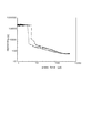
- the pressure sensor used for this measurement prepares a material in which a copper oxide thin film is formed by sputtering as a pressure-sensitive thin film 3 on a polyimide sheet cover film 5 and an adhesive sheet 12 that has been shaped in advance is bonded.
- the copper foil laminated on the base film 2 is etched to form the conductor pattern 4, and the photosensitive cover is laminated, exposed and developed.
- FIG. 7 shows a measurement example of the pressure detection characteristic of this pressure sensor.
- the horizontal axis is force (log scale), and the vertical axis is resistance value. It was confirmed that resistance changes depending on the pressure, and the pressure and pressure distribution can be measured with good reproducibility.
- FIG. 8 shows a second modification.
- (A) is a pattern of notches 10,
- (B) is a pattern of adhesive 12
- (C) is a covering pattern of spacers 7 and banks 8
- (D) is a conductor pattern 4
- (E) is an overlap of these patterns.
- the notch 10 of the cover film 5 is an I-shaped cut-out (see (A))
- the pressure-sensitive portion 51 having a hollow structure is formed on the spacer 7 by the adhesive 12 in two vertical and horizontal directions. It is a structure that is adhered by. When the free end of the pressure-sensitive portion 51 rides on the bank 8, it is possible to prevent unexpected contact between the electrodes 41 and 42 and the cover film 5.
- FIG. 9 shows a third modification.
- (A) is a pattern of notches 10,
- (B) is a pattern of adhesive 12,
- (C) is a covering pattern of spacers 7 and banks 8,
- (D) is a conductor pattern 4, and
- (E) is an overlap of these patterns.
- the notch 10 of the cover film 5 is T-shaped (see (A)), and when the cover film 5 is attached to the base film 2 via the spacer 7 by the adhesive 12, the hollow structure
- the pressure-sensitive portion 51 that receives the pressure is a cantilever structure, but the free end of the horizontal side is not on the bank 8. Since the electrodes 41 and 42 and the pressure-sensitive portion 51 having a hollow structure are easily brought into contact with each other, high sensitivity can be realized. Further, since the bank 8 surrounding the electrodes 41 and 42 is increased, the wiring area and the bonding area are reduced.
- FIG. 10 shows a fourth modification.
- (A) is a pattern of notches 10,
- (B) is a pattern of adhesive 12,
- (C) is a covering pattern of spacers 7 and banks 8,
- (D) is a conductor pattern 4, and
- (E) is an overlap of these patterns.
- the notch 10 of the cover film 5 is I-shaped (see (A)), and when the cover film 5 is attached to the base film 2 via the spacer 7 by the adhesive 12,
- the pressure-sensitive portion 51 having a hollow structure is bonded to the two sides in the vertical and horizontal directions, but the free end of the pressure-sensitive portion 51 is not on the bank 8 (see (E)). .
- the I-shaped cut simplifies the structure and allows a wide wiring area and bonding area.
- the electrodes 41 and 42 can be comb-shaped electrodes as shown in FIG.
- the reinforcing plate 13 can be formed by leaving a copper pattern on the back side of the pressure sensor 1. If reinforced in this way, the sensing performance of the pressure sensor 1 can be improved.
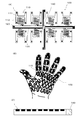
- FIGS. 12A to 12C show a pressure detection module using the pressure sensor of the present invention.
- the pressure detection module shown in FIG. 12C includes a flexible circuit board 110 having a single belt-like portion 111, and the above-described pressure sensor 1 of the present invention arranged in a plurality of belt-like portions constituting the flexible circuit board. It has a configuration with.
- the pressure sensor 1 is arranged in the side edge of each strip
- the pressure detection module 100 further includes one or more communication terminals 120 provided on the flexible circuit board 110 and a communication function provided on the flexible circuit board 110 and transmitting information of the pressure sensor 1 to the communication terminals. And at least two electronic circuit units 140.
- the flexible wiring board has heat resistance, can be mounted with components, and can mount electronic components and ICs where necessary. This enables signal processing and communication control around the pressure sensor. Since it is not necessary to connect to an external substrate, wiring can be reduced and the weight can be reduced. If necessary, a temperature sensor and other sensors can be mounted and used as a composite sensor module.
- a pressure detection module 100 shown in FIG. 12A includes a flexible circuit board 110 having a plurality of strip portions 111 and the above-described pressure sensor 1 of the present invention disposed on the strip portions constituting the flexible circuit board. It becomes the composition.
- the plurality of belt-like portions 111 are configured in a tree structure that branches hierarchically, and the pressure sensor 1 is provided at the end portion of each belt-like portion 111.
- the band-shaped portions of the tree structure are connected by the zigzag-shaped portion 112 so that the wiring portion between the pressure sensors 1 can be more easily deformed following the flexible surface.
- the pressure detection module 100 is further connected to the communication terminal 120 by one or more communication terminals 120 provided on the flexible circuit board 110 and wiring 130 provided on the flexible circuit board 110 and extending from the flexible circuit board 100. And one or more electronic circuit units 140 having a communication function for transmitting information of the plurality of pressure sensors 1 to the communication terminals.
- the form of the pressure detection module can be variously configured according to the application site. For example, in FIG. 12B, the pressure sensor is integrally formed at an arbitrary position of the strip-shaped flexible circuit board 110.
- the pressure sensor has a belt-like configuration and has a hollow portion that is open on one side.
- the pressure sensor may not have a belt-like configuration, and the hollow portion may not be open.
- a hollow part is formed in any part of the base film and cover film that constitute the flexible circuit board, an electrode is provided, a bank surrounding the electrode is provided, and a pressure-sensitive thin film corresponding to the hollow part is brought into contact according to pressure. Any configuration that can detect the pressure by the contact resistance method may be used. For example, as shown in FIG.
- the bank 8 is not provided, the end surface of the adhesive sheet 12 is retracted from the end surface of the spacer 7 made of a photosensitive cover, and the adhesive fluidized during thermocompression flows into the hollow portion. It is also possible to secure a holding area so as not to be present.
- the spacer 7 can also be used by using the photosensitive cover only as the bank 8 and sticking the cover film 5 and the base film 2 with the thick adhesive sheet 12 in other portions. good. Even if the pressure sensor is downsized, it is important that the adhesive does not flow into the hollow portion in order to avoid the influence of the adhesive flowing on the performance of the pressure sensor.
- the pressure sensor and the pressure detection module of the present invention mainly include pressure distributions such as curved surfaces including various spherical curved surfaces, in particular, flexible curved surfaces (hereinafter referred to as flexible curved surfaces) that have a small curvature and can undergo dynamic curvature changes. Suitable for applications that require low measurement errors and high resolution in measurement. For example, a human or robot body surface or an object surface in contact with the body surface is a typical measurement target.
- the main application fields are tactile sensors for fingers and soles (information device input devices, product development evaluation of hands), tactile sensors for robot hands and prosthetic hands, measurement of surface pressure distribution of chairs and beds (medical welfare, product development) Evaluation), pressure distribution measurement of the torso and limbs (medicine, exercise measurement, clothing development), etc. can be widely applied.
Landscapes
- Physics & Mathematics (AREA)
- General Physics & Mathematics (AREA)
- Chemical & Material Sciences (AREA)
- Analytical Chemistry (AREA)
- Measuring Fluid Pressure (AREA)
- Force Measurement Appropriate To Specific Purposes (AREA)
Abstract
フレキシブル回路基板の構成要素で成形でき、しかも、屈曲時の低計測誤差、高い柔軟性、小型高密度性、耐熱性などに優れる圧力センサ及びその製造方法並びに圧力検出モジュールを提供する。 一つ以上の電極を有する導電体パターン4が設けられたベースフィルム2と、導電体パターン4の電極を覆うようにベースフィルム2に積層されるカバーフィルム5と、カバーフィルム5とベースフィルム2間に設けられ、電極とカバーフィルム5の間に所定の隙間を有する中空部6を構成するスペーサ7と、電極とスペーサ7との間に土手8、を備え、カバーフィルム5の中空部6に対応する部分は、圧力に応じて電極に接離する方向に変形可能で、電極との接触圧に応じて接触抵抗が変化する感圧部を有し、接触抵抗の変化によって圧力を検出する構成となっている。
Description
本発明は、フレキシブル回路基板に一体的に形成可能で、球状曲面を含む柔軟曲面に用いる圧力分布の計測に適した圧力センサ及びその製造方法並びに圧力検出モジュールに関する。
市販されている一般的な圧力分布センサは、基本的に四角形状の薄いシートから構成されている。シート形状なので、筒状曲面での計測は可能であるが、球状曲面を含む柔軟曲面での計測には適さない。これは、(N×M)点の圧力点を(N+M)本の配線で信号収集する省配線技術(マトリクス配線)と関係しており、縦横する配線のため計測領域形状が四角形状などに制約されるためである。
また、これらの圧力分布センサは、PETフィルムと印刷配線で実装されたものが主流となっているが、配線の印刷精度やマイグレーションのため配線密度が低く、また配線に柔軟性がなく曲げ屈曲耐性がない。さらに、半田リフローにも適さないため、部品実装が困難であり、信号処理装置と大型コネクタで接続しなければならない問題も抱えている。
また、これらの圧力分布センサは、PETフィルムと印刷配線で実装されたものが主流となっているが、配線の印刷精度やマイグレーションのため配線密度が低く、また配線に柔軟性がなく曲げ屈曲耐性がない。さらに、半田リフローにも適さないため、部品実装が困難であり、信号処理装置と大型コネクタで接続しなければならない問題も抱えている。
これらの問題に対し、多様な曲面上でも圧力分布を計測可能な触覚センサを実現するものとして、帯状部を備えたツリー状基板からなり、またマトリクス配線ではなく、アナログ-デジタル変換や通信ができる小型ICなどをセンサシート上に部品実装したIC型省配線に基づく技術が提案されている(特許文献1参照)。
この特許文献1のツリー状基板では、帯状部に沿って圧力検出部と配線を敷設するため、スペースが狭く高密度配線が必要であり、またIC型省配線のために電子部品を基板上に直接実装する必要がある。
そのため、圧力検出は、上記したような一般的なPETフィルムと印刷配線による方法ではなく、一般的な電子機器に利用されているフレキシブル回路基板の利用が適している。
この特許文献1のツリー状基板では、帯状部に沿って圧力検出部と配線を敷設するため、スペースが狭く高密度配線が必要であり、またIC型省配線のために電子部品を基板上に直接実装する必要がある。
そのため、圧力検出は、上記したような一般的なPETフィルムと印刷配線による方法ではなく、一般的な電子機器に利用されているフレキシブル回路基板の利用が適している。
特許文献1では、圧力検出部に適用される圧力センサの構成は任意としているが、既存の圧力センサによると、計測誤差が生じ、柔軟性を高くできない、小型化が困難といった問題がある。
たとえば、一般的な圧力分布センサに用いられる圧力検出機構は、2枚のフィルムに感圧抵抗素材や弾性誘電体を挟み込んだ構造が主流となっている(たとえば、ニッタ(株)のFlexiForce(商品名)や Tekscan(商品名)等)。
しかし、このタイプの圧力分布センサは、屈曲すると内部圧力が発生してしまい、外部圧が作用した場合と区別がつかず、計測誤差が生じる。これは、各層の曲率が異なるため、屈曲部において互いに近づこうとしてセンサシートの法線方向に内部圧力が発生するもので、曲率が大きいほどその値は大きくなる。
スペーサとカバーフィルムの接着工程の際、接着剤がセンサ部へ流れ込むことで、電極の導電性を損ない、センサ特性を悪化させる。このため、小型化が困難である。特に、複数のセンサを高密度で実装する場合、限られた接着面積を有効活用し、かつ、電極部の中空構造を維持することは困難な課題である。
たとえば、一般的な圧力分布センサに用いられる圧力検出機構は、2枚のフィルムに感圧抵抗素材や弾性誘電体を挟み込んだ構造が主流となっている(たとえば、ニッタ(株)のFlexiForce(商品名)や Tekscan(商品名)等)。
しかし、このタイプの圧力分布センサは、屈曲すると内部圧力が発生してしまい、外部圧が作用した場合と区別がつかず、計測誤差が生じる。これは、各層の曲率が異なるため、屈曲部において互いに近づこうとしてセンサシートの法線方向に内部圧力が発生するもので、曲率が大きいほどその値は大きくなる。
スペーサとカバーフィルムの接着工程の際、接着剤がセンサ部へ流れ込むことで、電極の導電性を損ない、センサ特性を悪化させる。このため、小型化が困難である。特に、複数のセンサを高密度で実装する場合、限られた接着面積を有効活用し、かつ、電極部の中空構造を維持することは困難な課題である。
感圧抵抗素材を塗布する方式では、屈曲時にフィルム面に沿った伸張力が生じて誤差になることもある。屈曲時、特に動的に曲率が変化する場合、この内部圧力と本来計測したい外部圧力を区別することは非常に困難で、柔軟曲面における圧力分布計測の大きな誤差要因となっている。
また、マトリクス配線を使ったセンサや、弾性誘電体を挟み込んだ静電容量方式では、上下のフィルムに電極や配線が必要となるためセンサが厚くなり、屈曲性が悪化する問題がある。これは、センサの屈曲自体に外力を要することを意味し、本来計測したい外力に対する誤差にもなる。
また、マトリクス配線を使ったセンサや、弾性誘電体を挟み込んだ静電容量方式では、上下のフィルムに電極や配線が必要となるためセンサが厚くなり、屈曲性が悪化する問題がある。これは、センサの屈曲自体に外力を要することを意味し、本来計測したい外力に対する誤差にもなる。
圧力検出部には、このような感圧素材などを挟み込んだ方式以外に、部品として圧力検出素子を実装する方法もあるが、この場合、半田リフローや導電接着剤により取付けすることになるが、半田や接着剤の硬さ、屈曲による剥がれなど耐久性が低い。また、接着は実装コストが高い、などと言った問題がある。特に、半田の場合、パッド部やカバーレイの開口部のサイズ、取り付け誤差など、半田メッキ周辺に要する余分な領域が大きく、小型高密度化が難しいといった問題もある。
さらに、一般的な感圧抵抗は、導電粉をゴムなどのバインダーに分散したものが主流であるが、これらは耐熱性が高いとは言えない。カバーフィルムの接着工程やIC型省配線に必要な半田リフローと共存するには、一定の耐熱性も必要となるため、素材には注意が必要となる。
さらに、一般的な感圧抵抗は、導電粉をゴムなどのバインダーに分散したものが主流であるが、これらは耐熱性が高いとは言えない。カバーフィルムの接着工程やIC型省配線に必要な半田リフローと共存するには、一定の耐熱性も必要となるため、素材には注意が必要となる。
本発明は、上記した従来技術の問題点を解決するためになされたもので、その目的とするところは、フレキシブル回路基板の構成要素で成形でき、しかも、屈曲時の低計測誤差、高い柔軟性、小型高密度性、耐熱性などに優れる圧力センサ及びその製造方法並びに圧力検出モジュールを提供することを目的とする。
上記目的を達成するために、本発明の圧力センサは、
一つ以上の電極を有する導電体パターンが設けられたベースフィルムと、
該導電体パターンの電極を覆うようにベースフィルムに積層されるカバーフィルムと、
該カバーフィルムとベースフィルム間に設けられ、前記電極とカバーフィルムの間に所定の隙間を有する中空部を構成するスペーサと、を備え、
前記カバーフィルムの前記中空部に対応する部分は、圧力に応じて前記電極に接離する方向に変形可能で、前記電極との接触圧に応じて接触抵抗が変化する感圧部を有し、接触抵抗の変化によって圧力を検出する構成となっていることを特徴とする。
このようにすれば、センサが屈曲しても、屈曲変形は中空部によって吸収されるので、内部圧力の発生を軽減でき、計測誤差を低くすることができる。
また、電極を含む導電体パターンはベースフィルムだけで、厚さは薄く、柔軟で屈曲性がよいので、屈曲自体に要する外力は小さく、計測誤差をより低くできる。
電極を含む導電体パターンは、通常のフレキシブル回路基板の配線層と同様に成形できるので、小型で配線密度を高くすることができる。
さらに、接触抵抗方式としているので、耐熱性が高く、IC型省配線に必要なリフロー工程にも適している。
一つ以上の電極を有する導電体パターンが設けられたベースフィルムと、
該導電体パターンの電極を覆うようにベースフィルムに積層されるカバーフィルムと、
該カバーフィルムとベースフィルム間に設けられ、前記電極とカバーフィルムの間に所定の隙間を有する中空部を構成するスペーサと、を備え、
前記カバーフィルムの前記中空部に対応する部分は、圧力に応じて前記電極に接離する方向に変形可能で、前記電極との接触圧に応じて接触抵抗が変化する感圧部を有し、接触抵抗の変化によって圧力を検出する構成となっていることを特徴とする。
このようにすれば、センサが屈曲しても、屈曲変形は中空部によって吸収されるので、内部圧力の発生を軽減でき、計測誤差を低くすることができる。
また、電極を含む導電体パターンはベースフィルムだけで、厚さは薄く、柔軟で屈曲性がよいので、屈曲自体に要する外力は小さく、計測誤差をより低くできる。
電極を含む導電体パターンは、通常のフレキシブル回路基板の配線層と同様に成形できるので、小型で配線密度を高くすることができる。
さらに、接触抵抗方式としているので、耐熱性が高く、IC型省配線に必要なリフロー工程にも適している。
前記電極と前記スペーサの間に土手を設ければ、スペーサ上にカバーフィルムを接着する際に、中空部への、溶けた接着剤の流れ込みを防止することができ、接着剤による影響を排除できる。
前記電極を前記ベースフィルムに並べて配置される一対の電極として構成してもよいし、前記ベースフィルムに1つとし、感圧部と電気的に接続される構成とすることもできる。
前記電極を前記ベースフィルムに並べて配置される一対の電極として構成してもよいし、前記ベースフィルムに1つとし、感圧部と電気的に接続される構成とすることもできる。
ベースフィルムは帯状構成で、前記中空部はベースフィルムの一方の側縁に片側開放される構成とすれば、より柔軟性が高くなり、計測誤差を低くすることができる。
前記導電体パターンの中空部に露出する部分に、酸化防止用の金メッキ等の金属導体のメッキを施しておけば、電極の酸化による劣化を防止することができる。
また、メッキには、メッキマスクが必要であるが、感光性カバー等のスペーサで覆われた部分にはメッキがつかないため、感光性カバーと金属メッキによって、完全に銅箔等で形成される導電体パターンを保護することができる。
前記カバーフィルムに、屈曲時の引張り力を軽減するための切れ込みを設けておけば、屈曲時の内部圧力の発生をより一層軽減することができ、計測誤差を一層低くすることができる。
また、感圧部はカバーフィルムに成膜された感圧用薄膜としておけば、一般のフレキシブル回路基板の生産ライン内でラミネートできるので、特殊な実装工程を減らすことができ、低コスト化が実現できる。
前記スペーサまたは/および土手を、感光性カバーから構成すれば、マスクを使用した露光・現像によって微細な形状に加工できるため、任意に、覆う部分と覆わない部分を選択、作製でき、中空部や土手を、高精度に形成することができる。
カバーフィルム上に突起を付けておけば、カバーフィルムが中空部に押し込まれやすくなり、初期感度を高める効果が生まれる
前記導電体パターンの中空部に露出する部分に、酸化防止用の金メッキ等の金属導体のメッキを施しておけば、電極の酸化による劣化を防止することができる。
また、メッキには、メッキマスクが必要であるが、感光性カバー等のスペーサで覆われた部分にはメッキがつかないため、感光性カバーと金属メッキによって、完全に銅箔等で形成される導電体パターンを保護することができる。
前記カバーフィルムに、屈曲時の引張り力を軽減するための切れ込みを設けておけば、屈曲時の内部圧力の発生をより一層軽減することができ、計測誤差を一層低くすることができる。
また、感圧部はカバーフィルムに成膜された感圧用薄膜としておけば、一般のフレキシブル回路基板の生産ライン内でラミネートできるので、特殊な実装工程を減らすことができ、低コスト化が実現できる。
前記スペーサまたは/および土手を、感光性カバーから構成すれば、マスクを使用した露光・現像によって微細な形状に加工できるため、任意に、覆う部分と覆わない部分を選択、作製でき、中空部や土手を、高精度に形成することができる。
カバーフィルム上に突起を付けておけば、カバーフィルムが中空部に押し込まれやすくなり、初期感度を高める効果が生まれる
また、本発明の圧力センサの製造方法は、ベースフィルム上に一対の電極を備えた導電体パターンを形成し、
該ベースフィルムに感光性カバーを積層すると共に、少なくとも前記導電体パターンの一対の電極に対応する部分を除去して露出させ、感光性カバーの残存部分によって導電体パターンの残りの部分を覆い、
前記導電体パターンの一対の電極を含む露出部分について酸化防止用の金属メッキ処理を施し、
その後、前記電極との接触圧によって接触抵抗が変化する感圧部が予め形成されたカバーフィルムを積層し、前記感光性カバーの残存部分と接着剤にて貼り合わせることで、前記感光性カバーを除去した一対の電極に対応する部分に中空部を形成することを特徴とする。
感光性カバーの一対の電極に対応する部分を除去する際に、感光性カバーを利用し、前記中空部の手前に、中空部への接着剤の流れ込みを防止する土手を造形し、該土手にはカバーフィルムは非接着とすることを特徴とする。
また、他の製造方法は、ベースフィルム上に一つの電極を備えた導電体パターンを形成し、
該ベースフィルムに感光性カバーを積層すると共に、少なくとも前記導電体パターンの電極に対応する部分を除去して露出させ、感光性カバーの残存部分によって導電体パターンの残りの部分を覆い、
前記導電体パターンの電極を含む露出部分について酸化防止用の金属メッキ処理を施し、
その後、前記電極との接触圧によって接触抵抗が変化する感圧部および前記感圧部に電気的に接続された電極が予め形成されたカバーフィルムを積層し、前記感光性カバーの残存部分と接着剤にて貼り合わせることで、前記感光性カバーの除去した電極に対応する部分に中空部を形成することを特徴とする。
また、上記製造方法において、前記感光性カバーの前記ベースフィルム上の前記電極に対応する部分を除去する際に、感光性カバーを利用し、前記中空部の手前に、中空部への接着剤の流れ込みを防止する土手を造形し、該土手にはカバーフィルムは非接着とすることが好適である。
該ベースフィルムに感光性カバーを積層すると共に、少なくとも前記導電体パターンの一対の電極に対応する部分を除去して露出させ、感光性カバーの残存部分によって導電体パターンの残りの部分を覆い、
前記導電体パターンの一対の電極を含む露出部分について酸化防止用の金属メッキ処理を施し、
その後、前記電極との接触圧によって接触抵抗が変化する感圧部が予め形成されたカバーフィルムを積層し、前記感光性カバーの残存部分と接着剤にて貼り合わせることで、前記感光性カバーを除去した一対の電極に対応する部分に中空部を形成することを特徴とする。
感光性カバーの一対の電極に対応する部分を除去する際に、感光性カバーを利用し、前記中空部の手前に、中空部への接着剤の流れ込みを防止する土手を造形し、該土手にはカバーフィルムは非接着とすることを特徴とする。
また、他の製造方法は、ベースフィルム上に一つの電極を備えた導電体パターンを形成し、
該ベースフィルムに感光性カバーを積層すると共に、少なくとも前記導電体パターンの電極に対応する部分を除去して露出させ、感光性カバーの残存部分によって導電体パターンの残りの部分を覆い、
前記導電体パターンの電極を含む露出部分について酸化防止用の金属メッキ処理を施し、
その後、前記電極との接触圧によって接触抵抗が変化する感圧部および前記感圧部に電気的に接続された電極が予め形成されたカバーフィルムを積層し、前記感光性カバーの残存部分と接着剤にて貼り合わせることで、前記感光性カバーの除去した電極に対応する部分に中空部を形成することを特徴とする。
また、上記製造方法において、前記感光性カバーの前記ベースフィルム上の前記電極に対応する部分を除去する際に、感光性カバーを利用し、前記中空部の手前に、中空部への接着剤の流れ込みを防止する土手を造形し、該土手にはカバーフィルムは非接着とすることが好適である。
また、本発明の圧力検出モジュールは、1つ又は複数の帯状部を有するフレキシブル回路基板と、フレキシブル回路基板を構成する1つ又は複数の帯状部に配置された上記した圧力センサと、を備えた構成となっている。
このように、圧力センサをフレキシブル回路基板に組み込むことで、球状曲面などの立体的な形状に対しても圧力センサを密接させることができ、圧力分布を正確に検出することができる。
また、複数の帯状部を階層的に分岐しているツリー構造から構成し、各分岐帯状部の末端部位に圧力センサを設ければ、圧力センサの検出部位をより高密度に配置できる。
また、フレキシブル回路基板には、1つ以上の通信用端子と、フレキシブル回路基板に設けられた配線によって前記圧力センサ及び通信用端子に電気的に接続され、各圧力センサにより取得された情報を受信し、当該情報を通信用端子に送信する通信機能を有する1つ以上の電子回路部と、を備えた構造とすることもできる。
このように、圧力センサをフレキシブル回路基板に組み込むことで、球状曲面などの立体的な形状に対しても圧力センサを密接させることができ、圧力分布を正確に検出することができる。
また、複数の帯状部を階層的に分岐しているツリー構造から構成し、各分岐帯状部の末端部位に圧力センサを設ければ、圧力センサの検出部位をより高密度に配置できる。
また、フレキシブル回路基板には、1つ以上の通信用端子と、フレキシブル回路基板に設けられた配線によって前記圧力センサ及び通信用端子に電気的に接続され、各圧力センサにより取得された情報を受信し、当該情報を通信用端子に送信する通信機能を有する1つ以上の電子回路部と、を備えた構造とすることもできる。
以上説明したように、本発明によれば、中空部が形成されているので、高い柔軟性が得られ、屈曲の影響が少なく、計測誤差を小さくできる。
また、導電体パターンは、従来のフレキシブル回路基板の配線層と同様に高密度性を実現でき、小型化を図ることができる。
さらに、接触抵抗を利用しているので、耐熱性にも優れ、半田リフロー等にも適用可能である。
また、フレキシブル回路基板に用いられる材料で構成されるので、従来のフレキシブル回路基板の製造設備によって、容易に製造することができる。
また、導電体パターンは、従来のフレキシブル回路基板の配線層と同様に高密度性を実現でき、小型化を図ることができる。
さらに、接触抵抗を利用しているので、耐熱性にも優れ、半田リフロー等にも適用可能である。
また、フレキシブル回路基板に用いられる材料で構成されるので、従来のフレキシブル回路基板の製造設備によって、容易に製造することができる。
[概念構成]
まず、本発明を実施するための概念構成について説明する。
本発明の圧力センサは、接触抵抗方式にもとづく検出原理を導入し、これをフレキシブル回路基板の内部に直接埋め込んだ構造とする。
具体的には、圧力センサを、ベースフィルム、フィルムカバー、感光性カバー(PSC:Photo-Sensitive Cover)など、汎用的なフレキシブル回路基板の構成素材で構築することで、フレキシブル回路基板の内部に圧力センサを埋め込む構造を実現する。
この圧力センサは、土手による接着剤の電極への流れ込み防止によって圧力検出部を小型に構成できるため高密度化に適するだけでなく、中空構造を導入することで、屈曲時の内部圧力を抑制する。さらに、電極を片面に集約することで、薄さや柔軟性を高める。また、接触抵抗方式は耐熱性があり、IC型省配線に必要なリフロー工程にも適している。
これにより、薄さと柔軟性が高まり計測精度が向上するだけでなく、半田パッドなどの取付け部位を不要とし、小型高密度化や耐久性を高める。
さらに、圧力センサについて、既存のフレキシブル回路基板の製造工程を大きく変更することなく、低コストで実現できるようにする。
まず、本発明を実施するための概念構成について説明する。
本発明の圧力センサは、接触抵抗方式にもとづく検出原理を導入し、これをフレキシブル回路基板の内部に直接埋め込んだ構造とする。
具体的には、圧力センサを、ベースフィルム、フィルムカバー、感光性カバー(PSC:Photo-Sensitive Cover)など、汎用的なフレキシブル回路基板の構成素材で構築することで、フレキシブル回路基板の内部に圧力センサを埋め込む構造を実現する。
この圧力センサは、土手による接着剤の電極への流れ込み防止によって圧力検出部を小型に構成できるため高密度化に適するだけでなく、中空構造を導入することで、屈曲時の内部圧力を抑制する。さらに、電極を片面に集約することで、薄さや柔軟性を高める。また、接触抵抗方式は耐熱性があり、IC型省配線に必要なリフロー工程にも適している。
これにより、薄さと柔軟性が高まり計測精度が向上するだけでなく、半田パッドなどの取付け部位を不要とし、小型高密度化や耐久性を高める。
さらに、圧力センサについて、既存のフレキシブル回路基板の製造工程を大きく変更することなく、低コストで実現できるようにする。
以下に図面を参照して、この発明を実施するための形態を例示的に詳しく説明する。ただし、以下の実施形態に記載されている構成部品の寸法、材質、形状、その相対配置などは、特に特定的な記載がない限りは、この発明の範囲をそれらのみに限定する趣旨のものではない。
[実施の形態]
<1:圧力センサの概略構成>
まず、図1を参照して、本実施の形態に係る圧力センサ1の概略構成について説明する。
図1(A)はカバーフィルムを外して示す模式的斜視図、(B)は(A)のカバーフィルムを積層した状態の模式的斜視図、(C)は模式的断面図である。
[実施の形態]
<1:圧力センサの概略構成>
まず、図1を参照して、本実施の形態に係る圧力センサ1の概略構成について説明する。
図1(A)はカバーフィルムを外して示す模式的斜視図、(B)は(A)のカバーフィルムを積層した状態の模式的斜視図、(C)は模式的断面図である。
[基本構成]
図1に示すように、本実施形態に係る圧力センサ1は、フレキシブル回路基板を構成する導電体パターン4が形成されたベースフィルム2とカバーフィルム5の任意の位置に、中空部6を構成し、その内部に一対の電極41、42を構成したものである。そして、カバーフィルム5の電極41,42と対面する面に、感圧用薄膜3を成膜することで、圧力がかかったときの接触抵抗の変化を検出する圧力検出部を構成する。
中空部6を構成するために、ベースフィルム2とカバーフィルム5の間に、中空部6を取り囲むように土手8、さらにそれを囲むようにスペーサ7が介装されている。なお、図示例では、カバーフィルム5にスリット10が設けられている。このスリット10については、後述する。
図1に示すように、本実施形態に係る圧力センサ1は、フレキシブル回路基板を構成する導電体パターン4が形成されたベースフィルム2とカバーフィルム5の任意の位置に、中空部6を構成し、その内部に一対の電極41、42を構成したものである。そして、カバーフィルム5の電極41,42と対面する面に、感圧用薄膜3を成膜することで、圧力がかかったときの接触抵抗の変化を検出する圧力検出部を構成する。
中空部6を構成するために、ベースフィルム2とカバーフィルム5の間に、中空部6を取り囲むように土手8、さらにそれを囲むようにスペーサ7が介装されている。なお、図示例では、カバーフィルム5にスリット10が設けられている。このスリット10については、後述する。
このように、圧力センサ1を構成するためには、ポリイミドフィルム等のベースフィルム2とカバーフィルム5の、2枚のフィルムで、電極41,42を挟み込み、スペーサ7に接着する。
スペーサ7は、カバーフィルム5を接着する接着剤、もしくは、非接着性のスペーサ素材に接着剤を積層させたものなどで構成される。
カバーフィルム5を相手材に貼り合わせる場合、予め接着剤を塗布あるいは形状加工した接着剤シートを貼り合わせた積層体を構成し、温度・圧力をかけて相手材とのラミネートを行う。これによって一度に、大面積かつ高精度に多数の圧力センサを製造することができる。
ところが、接着剤はラミネート時の熱により接着剤が軟化し周辺部に流れ出し出すため中空構造にしたい部分に流れ出し、その中空部6を塞いだり、狭くしてしまったりという問題があるために、感光性カバーや印刷インクなどを利用して土手8を造形し、土手8によって接着剤の流れ込みを防止する。
スペーサ7は、カバーフィルム5を接着する接着剤、もしくは、非接着性のスペーサ素材に接着剤を積層させたものなどで構成される。
カバーフィルム5を相手材に貼り合わせる場合、予め接着剤を塗布あるいは形状加工した接着剤シートを貼り合わせた積層体を構成し、温度・圧力をかけて相手材とのラミネートを行う。これによって一度に、大面積かつ高精度に多数の圧力センサを製造することができる。
ところが、接着剤はラミネート時の熱により接着剤が軟化し周辺部に流れ出し出すため中空構造にしたい部分に流れ出し、その中空部6を塞いだり、狭くしてしまったりという問題があるために、感光性カバーや印刷インクなどを利用して土手8を造形し、土手8によって接着剤の流れ込みを防止する。
また、ベースフィルム2やカバーフィルム5として、フレキシブル回路基板の一般的な材料であるポリイミドは、水分や酸素を透過するため、電極等41,42を含む導電体パターン4をスペーサ7、メッキ9のいずれかによって保護することにより、製造工程中および使用時に酸化してしまうということを防ぐことができる。
[各部詳細構成]
次に、ここで挙げた各層について、さらに詳しく説明する。
[ベースフィルム2、カバーフィルム5について]
ベースフィルム2及びカバーフィルム5には、ポリイミドフィルムが用いられる。もちろん、ポリイミドフィルムに限られず、例えば、ポリエステル、ポリアミド、ポリカーボネート、ポリアリレート、ポリフェニレンエーテル、ポリフェニレンスルフィド、ポリエーテルスルホン、ポリエーテルイミド、液晶ポリマー、ポリエーテルエーテルケトン、環状ポリオレフィン、ポリアミドイミド、熱可塑性ポリイミド、ポリエチレンテレフタレート、シクロオレフィンポリマーから選ばれる1種からなるフィルム、又は複数の樹脂フィルムを積層した積層フィルムを用いることができる。
なお、ベースフィルム2及びカバーフィルム5は同一幅の細い帯状構成で、その厚さは5~100μmが好ましく、特に5~50μmであるとよい。
ベースフィルム2及びカバーフィルム5に用いられる材料は、同じ材料であってもよいし、それぞれ異なる材料が選択されてもよい。
次に、ここで挙げた各層について、さらに詳しく説明する。
[ベースフィルム2、カバーフィルム5について]
ベースフィルム2及びカバーフィルム5には、ポリイミドフィルムが用いられる。もちろん、ポリイミドフィルムに限られず、例えば、ポリエステル、ポリアミド、ポリカーボネート、ポリアリレート、ポリフェニレンエーテル、ポリフェニレンスルフィド、ポリエーテルスルホン、ポリエーテルイミド、液晶ポリマー、ポリエーテルエーテルケトン、環状ポリオレフィン、ポリアミドイミド、熱可塑性ポリイミド、ポリエチレンテレフタレート、シクロオレフィンポリマーから選ばれる1種からなるフィルム、又は複数の樹脂フィルムを積層した積層フィルムを用いることができる。
なお、ベースフィルム2及びカバーフィルム5は同一幅の細い帯状構成で、その厚さは5~100μmが好ましく、特に5~50μmであるとよい。
ベースフィルム2及びカバーフィルム5に用いられる材料は、同じ材料であってもよいし、それぞれ異なる材料が選択されてもよい。
[導電体パターン]
導電体パターン4を構成する電極41,42は、ベースフィルム2の一側縁に沿って、長手方向に所定隙間を介して互いに離間して直列に配置された平面電極によって構成されている。また、図2(B)に示すように、ベースフィルム2の他方の側縁側には、複数本の配線層43が延びている。
電極41,42が設けられる中空部6は、ベースフィルム2の一方の電極41,42側の側縁に片寄った位置に設けられ、側縁に開放されている。この例では、ベースフィルム2の長手方向に長い矩形状で、一方の長辺が開放側の側縁で、長手方向両端の端辺が開放側の側縁に対して直角に延びており、他方の長辺が開放側の側縁と平行に延びている。
電極41,42は、銅や銀、アルミニウム等の公知の金属又はカーボンなどの導体によって導電体パターン4として一体的に構成される。この実施例では、導電体パターン4は、ベースフィルム2の表面に、接着剤11を介して積層した圧延銅箔又は電解銅箔をエッチング加工する、所謂サブトラクティブ法にて形成する。その他の導電体パターン4の形成方法としては、ベースフィルム2上に、銅のような金属を用いて、蒸着またはスパッタ、湿式メッキ等の方法の他、銀またはナノカーボン等を含む導電性ペーストの印刷により形成することもできる。
導電体パターン4を構成する電極41,42は、ベースフィルム2の一側縁に沿って、長手方向に所定隙間を介して互いに離間して直列に配置された平面電極によって構成されている。また、図2(B)に示すように、ベースフィルム2の他方の側縁側には、複数本の配線層43が延びている。
電極41,42が設けられる中空部6は、ベースフィルム2の一方の電極41,42側の側縁に片寄った位置に設けられ、側縁に開放されている。この例では、ベースフィルム2の長手方向に長い矩形状で、一方の長辺が開放側の側縁で、長手方向両端の端辺が開放側の側縁に対して直角に延びており、他方の長辺が開放側の側縁と平行に延びている。
電極41,42は、銅や銀、アルミニウム等の公知の金属又はカーボンなどの導体によって導電体パターン4として一体的に構成される。この実施例では、導電体パターン4は、ベースフィルム2の表面に、接着剤11を介して積層した圧延銅箔又は電解銅箔をエッチング加工する、所謂サブトラクティブ法にて形成する。その他の導電体パターン4の形成方法としては、ベースフィルム2上に、銅のような金属を用いて、蒸着またはスパッタ、湿式メッキ等の方法の他、銀またはナノカーボン等を含む導電性ペーストの印刷により形成することもできる。
接着剤11は、熱可塑性ポリイミド等の公知の熱可塑性樹脂、またはシアネートエステル系樹脂、ポリフェニレンエーテル系樹脂、フェノール系樹脂、ナフタレン樹脂、ユリア樹脂、アミノ樹脂、アルキッド樹脂、ケイ素樹脂、フラン樹脂、不飽和ポリエステル樹脂、エポキシ樹脂、及びポリウレタン樹脂等の公知の熱硬化性樹脂を用いて形成される。あるいは、接着剤11は、上述の有機樹脂に、シリカまたはアルミナ等の無機フィラーを分散させたもので形成することもできる。
[接触抵抗方式の導入]
この実施例では、感圧部として、カバーフィルム5に感圧用薄膜3が成膜されている。この感圧用薄膜3は、有機、無機材料を問わず電極と接触することにより接触抵抗変化を生じる材料により構成されている。
この例では、ポリイミドフィルムからなるカバーフィルム5上に酸化銅や硫化銅などの感圧用薄膜3を形成したものと、FPCの銅配線を利用した電極41、42の表面に金メッキを施した導体を組み合わせることで、圧力センサを構成している。
すなわち、導電体同士には接触抵抗が存在するが、一般に圧力の増減で接触抵抗が増減するため、圧力検出に利用できる。しかし、銅と銅の接触抵抗では、わずかな圧力で抵抗値が大きく低下するため、ダイナミックレンジがでず、圧力検出用として利用するのは難しい。
この実施例では、感圧部として、カバーフィルム5に感圧用薄膜3が成膜されている。この感圧用薄膜3は、有機、無機材料を問わず電極と接触することにより接触抵抗変化を生じる材料により構成されている。
この例では、ポリイミドフィルムからなるカバーフィルム5上に酸化銅や硫化銅などの感圧用薄膜3を形成したものと、FPCの銅配線を利用した電極41、42の表面に金メッキを施した導体を組み合わせることで、圧力センサを構成している。
すなわち、導電体同士には接触抵抗が存在するが、一般に圧力の増減で接触抵抗が増減するため、圧力検出に利用できる。しかし、銅と銅の接触抵抗では、わずかな圧力で抵抗値が大きく低下するため、ダイナミックレンジがでず、圧力検出用として利用するのは難しい。
これに対し、硫化銅や酸化銅などの半導体と、銀や金といった導体の組み合わせによる接触抵抗では、低圧力時の接触抵抗が数KΩ~数MΩであり、圧力が増すにつれて数Ω~数KΩへと変化するため、非常にダイナミックレンジが大きくできるという特徴がある。
フィルムに感圧用薄膜3を形成する手法としては、ポリイミドフィルムに酸化銅などをスパッタリングや蒸着などで皮膜化する方法や、ポリイミドフィルム上に貼り合わせた銅箔を酸化することで表面を酸化銅にする方法、あるいは銅インクや亜酸化銅インクを印刷または塗布して大気中で加熱することで酸化銅を形成することができる。
このように、感圧用薄膜3を成膜したカバーフィルム5を用意すれば、一般のFPCの生産ライン内でラミネートでき、特殊な実装工程を減らすことができ、低コスト化が実現できる。
フィルムに感圧用薄膜3を形成する手法としては、ポリイミドフィルムに酸化銅などをスパッタリングや蒸着などで皮膜化する方法や、ポリイミドフィルム上に貼り合わせた銅箔を酸化することで表面を酸化銅にする方法、あるいは銅インクや亜酸化銅インクを印刷または塗布して大気中で加熱することで酸化銅を形成することができる。
このように、感圧用薄膜3を成膜したカバーフィルム5を用意すれば、一般のFPCの生産ライン内でラミネートでき、特殊な実装工程を減らすことができ、低コスト化が実現できる。
[スペーサ7]
スペーサ7は、感光性カバーや印刷インクなどとし、スペーサ7とカバーフィルム5の間は接着剤12により接着される。接着剤12の材料は、接着剤11と同じものが使用できる。スペーサ7を接着剤とし、接着剤12と同一のものとしても構成できる。
感光性カバーは、高精度に銅配線の上に保護膜を形成することができるが、2枚のポリイミドフィルムを接着するためには使われない光硬化樹脂である。
一般的には、カバーレイとして、ポリイミドフィルム等のフィルムカバーと感光性カバーとは目的に合わせ別々に使用される。機械的あるいは化学的な強度が要求される場合は、フィルムカバーが使用され、実装部品周辺部の寸法公差が要求され、機械的あるいは化学的な強度がそれほど要求されない場合に、感光性カバーが使用される。合わせて使用される場合は、フィルムカバーをラミネートし、カバーされていない領域に感光性カバーが部分的に使用される場合がある。
本実施の形態では、カバーレイとして、ポリイミドのカバーフィルム5とスペーサ7として作用する感光性カバーの二層構造として使用し、まず、中空構造内部に構成する電極部を除いて感光性カバーによって電極41,42を含む導電体パターン4の露出領域を保護する。
感光性カバーは、マスクを使用した露光・現像によって微細な形状に加工できるため、任意に、覆う部分と覆わない部分を選択、作製でき、高い寸法精度も実現できる。
スペーサ7は、感光性カバーや印刷インクなどとし、スペーサ7とカバーフィルム5の間は接着剤12により接着される。接着剤12の材料は、接着剤11と同じものが使用できる。スペーサ7を接着剤とし、接着剤12と同一のものとしても構成できる。
感光性カバーは、高精度に銅配線の上に保護膜を形成することができるが、2枚のポリイミドフィルムを接着するためには使われない光硬化樹脂である。
一般的には、カバーレイとして、ポリイミドフィルム等のフィルムカバーと感光性カバーとは目的に合わせ別々に使用される。機械的あるいは化学的な強度が要求される場合は、フィルムカバーが使用され、実装部品周辺部の寸法公差が要求され、機械的あるいは化学的な強度がそれほど要求されない場合に、感光性カバーが使用される。合わせて使用される場合は、フィルムカバーをラミネートし、カバーされていない領域に感光性カバーが部分的に使用される場合がある。
本実施の形態では、カバーレイとして、ポリイミドのカバーフィルム5とスペーサ7として作用する感光性カバーの二層構造として使用し、まず、中空構造内部に構成する電極部を除いて感光性カバーによって電極41,42を含む導電体パターン4の露出領域を保護する。
感光性カバーは、マスクを使用した露光・現像によって微細な形状に加工できるため、任意に、覆う部分と覆わない部分を選択、作製でき、高い寸法精度も実現できる。
[導電体パターン4の露出部のメッキ]
感圧用薄膜3と対向する電極41,42は、劣化を防ぐために金メッキなどメッキ9を施すのが望ましい。通常、金メッキ等のメッキ処理は、カバーレイなどが施された最終に近い段階で行われるが、本方式の場合、カバーフィルム5を張り合わせる前の段階で行う。この場合、電極41,42以外の配線部分も露出しているため全面に金メッキがなされる。全面が金メッキされると、コストがかかり、Niメッキでは、柔軟性が損なわれ、耐久性が悪化する。
そのため、電極41、42以外の配線部分はメッキから保護するのが望ましい。通常は粘着シールなどでマスクするが、高分解能な小型の圧力検出素子を構成するためには、粘着シールでのマスクは位置精度がでないため困難である。そこで、薄い感光性カバーによりカバーする方法を導入することが望ましい。
スペーサ7として感光性カバーを用いた場合には、それをメッキマスクとして使用することもできる。
感圧用薄膜3と対向する電極41,42は、劣化を防ぐために金メッキなどメッキ9を施すのが望ましい。通常、金メッキ等のメッキ処理は、カバーレイなどが施された最終に近い段階で行われるが、本方式の場合、カバーフィルム5を張り合わせる前の段階で行う。この場合、電極41,42以外の配線部分も露出しているため全面に金メッキがなされる。全面が金メッキされると、コストがかかり、Niメッキでは、柔軟性が損なわれ、耐久性が悪化する。
そのため、電極41、42以外の配線部分はメッキから保護するのが望ましい。通常は粘着シールなどでマスクするが、高分解能な小型の圧力検出素子を構成するためには、粘着シールでのマスクは位置精度がでないため困難である。そこで、薄い感光性カバーによりカバーする方法を導入することが望ましい。
スペーサ7として感光性カバーを用いた場合には、それをメッキマスクとして使用することもできる。
[土手の構造(接着剤流入防止)]
この実施の形態では、スペーサ7が被覆されたベースフィルム2に、カバーフィルム5が接着剤12によって貼り合わされて、電極露出領域に中空部6が構成される。接着剤12は常温では固体だが高温化で流動化させ2枚のフィルムに密着させた状態で熱硬化することで接着される。
接触抵抗方式では、感圧用薄膜3と電極41,42が分離している必要があるが、圧力検知部以外では2枚のフィルムは接着されている必要がある。この場合、圧力検知部のみ接着剤を取り除いてから2枚のフィルムを熱接着すればよいが、高温状態では接着剤が流動化し感圧検知部に流れ込んでしまう。
そこで、前もって圧力検知部の周りに土手8によって囲いを作ることにより、液状化した接着剤が流れ込んでくるのを防ぐことができる。本実施の形態のように、感光性カバーを用いると加工精度や位置精度を高く土手8の構造を作製できる。
また、このような土手8のような構造は、圧力検知部が無負荷時に電極41,42に接触してしまうのを防ぐ役目も果たすことができる。
この例では、矩形状の中空部の3辺を取り囲むように、コ字形状に形成される。
このように構成した圧力センサ1における感光性カバーによるスペーサ7、導電体パターンの保護、土手8による接着剤流入防止等の使用方法、構造は、本発明独自の技術であり、量産性を損なうことなく実現でき、従来にない大面積、高密度で安価な圧力センサを製造できる。
この実施の形態では、スペーサ7が被覆されたベースフィルム2に、カバーフィルム5が接着剤12によって貼り合わされて、電極露出領域に中空部6が構成される。接着剤12は常温では固体だが高温化で流動化させ2枚のフィルムに密着させた状態で熱硬化することで接着される。
接触抵抗方式では、感圧用薄膜3と電極41,42が分離している必要があるが、圧力検知部以外では2枚のフィルムは接着されている必要がある。この場合、圧力検知部のみ接着剤を取り除いてから2枚のフィルムを熱接着すればよいが、高温状態では接着剤が流動化し感圧検知部に流れ込んでしまう。
そこで、前もって圧力検知部の周りに土手8によって囲いを作ることにより、液状化した接着剤が流れ込んでくるのを防ぐことができる。本実施の形態のように、感光性カバーを用いると加工精度や位置精度を高く土手8の構造を作製できる。
また、このような土手8のような構造は、圧力検知部が無負荷時に電極41,42に接触してしまうのを防ぐ役目も果たすことができる。
この例では、矩形状の中空部の3辺を取り囲むように、コ字形状に形成される。
このように構成した圧力センサ1における感光性カバーによるスペーサ7、導電体パターンの保護、土手8による接着剤流入防止等の使用方法、構造は、本発明独自の技術であり、量産性を損なうことなく実現でき、従来にない大面積、高密度で安価な圧力センサを製造できる。
[センサ部に突起]
本センサはフィルムのように薄型という特徴を持っているが、中空構造のために、初期加重が必要となる。より高い感度が要求される場合には、中空部6の上のカバーフィルム5上に小さな突起をつけると、カバーフィルム5が中空部分に押し込まれやすくなり、初期感度を高める効果が生まれる。
圧力検出部のカバーフィルム5の感圧用薄膜3の裏面上部に数μm~数十μm高さの突起を形成し、その突起が外部から押されることでわずかな圧力でも検知できるよう高感度化も可能である。
突起は、印刷、樹脂、接着剤、エッチングした銅箔、フィルムのパンチングなどにより形成する方法が考えられる。
本センサはフィルムのように薄型という特徴を持っているが、中空構造のために、初期加重が必要となる。より高い感度が要求される場合には、中空部6の上のカバーフィルム5上に小さな突起をつけると、カバーフィルム5が中空部分に押し込まれやすくなり、初期感度を高める効果が生まれる。
圧力検出部のカバーフィルム5の感圧用薄膜3の裏面上部に数μm~数十μm高さの突起を形成し、その突起が外部から押されることでわずかな圧力でも検知できるよう高感度化も可能である。
突起は、印刷、樹脂、接着剤、エッチングした銅箔、フィルムのパンチングなどにより形成する方法が考えられる。
[対極構造]
以上の説明では、電極41、42をベースフィルム2上のみに構成する例を示したが、1つの電極をベースフィルム2、もう1つの電極をカバーフィルム5に設けてもよい。電極の上に感圧用薄膜3を構成することもできる。この場合、屈曲性は悪くなるが、電極の面積を大きくすることができ、感度を高めることが可能となる。
以上の説明では、電極41、42をベースフィルム2上のみに構成する例を示したが、1つの電極をベースフィルム2、もう1つの電極をカバーフィルム5に設けてもよい。電極の上に感圧用薄膜3を構成することもできる。この場合、屈曲性は悪くなるが、電極の面積を大きくすることができ、感度を高めることが可能となる。
[囲み]
なお、中空部については、側面の片側開放構造のみならず、中空部が密閉された構成としてもよい。
同様に、土手8は、コの字形状のみならず、電極をすべて囲む構成でもよい。
なお、中空部については、側面の片側開放構造のみならず、中空部が密閉された構成としてもよい。
同様に、土手8は、コの字形状のみならず、電極をすべて囲む構成でもよい。
[製造方法]
次に、上記圧力センサの製造方法について、図2及び図3を参照して説明する。
電極との接触圧によって接触抵抗が変化する感圧用薄膜3が予め形成されたカバーフィルム5を予め準備しておく。
まず、ベースフィルム2上に、前述したとおり、サブトラクティブ法等によって、一対の電極41,42及び各種配線層43を含む導電体パターン4を形成する(図2(A)、(B)、図3(A)、(B)参照)。
次に、導電体パターン4が形成されたベースフィルム2に、スペーサ7及び土手8となる感光性カバーを積層する。そして、少なくとも導電体パターン4の一対の電極41,42に対応する部分を露出させるため感光性カバーを露光・現像し、感光性カバーの残存部分によって導電体パターン4の残りの部分を被覆する(図2(C)、図3(C)参照)。
次いで、導電体パターン4の一対の電極41,42を含む露出部分について酸化防止用の金属メッキ処理を施す(図示せず)。
次に、予め準備したカバーフィルム5を積層し、スペーサ7を介してベースフィルム2を、接着剤12にて貼り合わせることで、スペーサ7が介在しない一対の電極41、42の露出部に中空部6を形成する(図2(D)、(E)、図3(D)、(E)参照)。
また、感光性カバーからスペーサ7を形成する際に、中空部6を取り囲むように土手8を造形しておき、中空部6への接着剤12の流れ込みを防止する。土手8はカバーフィルム5と非接着とする。
次に、上記圧力センサの製造方法について、図2及び図3を参照して説明する。
電極との接触圧によって接触抵抗が変化する感圧用薄膜3が予め形成されたカバーフィルム5を予め準備しておく。
まず、ベースフィルム2上に、前述したとおり、サブトラクティブ法等によって、一対の電極41,42及び各種配線層43を含む導電体パターン4を形成する(図2(A)、(B)、図3(A)、(B)参照)。
次に、導電体パターン4が形成されたベースフィルム2に、スペーサ7及び土手8となる感光性カバーを積層する。そして、少なくとも導電体パターン4の一対の電極41,42に対応する部分を露出させるため感光性カバーを露光・現像し、感光性カバーの残存部分によって導電体パターン4の残りの部分を被覆する(図2(C)、図3(C)参照)。
次いで、導電体パターン4の一対の電極41,42を含む露出部分について酸化防止用の金属メッキ処理を施す(図示せず)。
次に、予め準備したカバーフィルム5を積層し、スペーサ7を介してベースフィルム2を、接着剤12にて貼り合わせることで、スペーサ7が介在しない一対の電極41、42の露出部に中空部6を形成する(図2(D)、(E)、図3(D)、(E)参照)。
また、感光性カバーからスペーサ7を形成する際に、中空部6を取り囲むように土手8を造形しておき、中空部6への接着剤12の流れ込みを防止する。土手8はカバーフィルム5と非接着とする。
[圧力センサの作用]
次に、本実施の形態に係る圧力センサの作用について説明する。
一対の電極41,42は不図示の電流源に接続されている。圧力が作用していない状態では、カバーフィルム5の中空部6に対応する感圧部分51と電極42とは離れており、電極41、42間には電流は流れない。
所定の圧力が作用すると、中空部6に対応する感圧部分51がたわみ変形して感圧用薄膜3が電極41,42に接触し、接触圧に応じて接触抵抗が変化し、電極間に流れる電流が変化する。
感圧用薄膜3に感圧抵抗素材を用いた場合は、接触抵抗に加えて、感圧用薄膜3自身の圧力による電気抵抗の変化により、抵抗値が大きく変化し、この電気抵抗の変化を電気信号として取り出し、圧力を検出する。
また、単純に屈曲して感圧部分51が変形したとしても、中空部6の初期隙間によってある程度変形が吸収されるので、屈曲による計測誤差は軽減される。
ベースフィルム2は帯状構成で、前記中空部6はベースフィルム2の一方の側縁に片側開放されているので、感圧部分51が圧力変化に応じて変形しやすい。また、中空部6内の空気は外部と流通するので、感圧部分51の変形を阻害しない。
次に、本実施の形態に係る圧力センサの作用について説明する。
一対の電極41,42は不図示の電流源に接続されている。圧力が作用していない状態では、カバーフィルム5の中空部6に対応する感圧部分51と電極42とは離れており、電極41、42間には電流は流れない。
所定の圧力が作用すると、中空部6に対応する感圧部分51がたわみ変形して感圧用薄膜3が電極41,42に接触し、接触圧に応じて接触抵抗が変化し、電極間に流れる電流が変化する。
感圧用薄膜3に感圧抵抗素材を用いた場合は、接触抵抗に加えて、感圧用薄膜3自身の圧力による電気抵抗の変化により、抵抗値が大きく変化し、この電気抵抗の変化を電気信号として取り出し、圧力を検出する。
また、単純に屈曲して感圧部分51が変形したとしても、中空部6の初期隙間によってある程度変形が吸収されるので、屈曲による計測誤差は軽減される。
ベースフィルム2は帯状構成で、前記中空部6はベースフィルム2の一方の側縁に片側開放されているので、感圧部分51が圧力変化に応じて変形しやすい。また、中空部6内の空気は外部と流通するので、感圧部分51の変形を阻害しない。
[切れ込みによる内部圧力の低減化]
また、カバーフィルム5に切れ込み10を入れているので、屈曲時のカバーフィルム5に作用する引張力を軽減できるため、結果として屈曲による内部圧力が減少することになる。
また、カバーフィルム5に切れ込み10を入れているので、屈曲時のカバーフィルム5に作用する引張力を軽減できるため、結果として屈曲による内部圧力が減少することになる。
図4には、圧力センサのカバーフィルム5をI字カットする場合と、L字状のカットする場合の切れ込みの形態を模式的に示している。
図4(A)、(B)は、I字カットの例である。図1の切れ込み10は、このI字カットの例であり、図5(A)は図1の圧力センサの平面図である。 切れ込み10は、中空部に対応する矩形状の感圧部分51を、開放側の側縁から直角に直線状にカットしている。引張力が完全にキャンセルできない。その代わり、製造自体は簡単と言える。図4では切れ込み10が反対側縁まで突っ切っていないが、突っ切りとすることも可能である。
図4(C)、(D)は、L字カットの例である。図5(B)は、図1の切れ込みをL字カットとした構成例である。 切れ込み10はL字形状で、中空部に対応する矩形状の感圧部分51を、開放側の側縁から直角に延びる横スリット10aと、横スリット10bとによって構成される。
このようにL型に切れ込み10を入れると、中空部に対応する感圧部分51が、片持ち状態となり、屈曲時の内部圧力をほぼゼロにすることが可能である。内部圧力を完全にキャンセルできる半面、切れ込み加工が難しく、状況に応じて、両者を使い分ける。
図4(A)、(B)は、I字カットの例である。図1の切れ込み10は、このI字カットの例であり、図5(A)は図1の圧力センサの平面図である。 切れ込み10は、中空部に対応する矩形状の感圧部分51を、開放側の側縁から直角に直線状にカットしている。引張力が完全にキャンセルできない。その代わり、製造自体は簡単と言える。図4では切れ込み10が反対側縁まで突っ切っていないが、突っ切りとすることも可能である。
図4(C)、(D)は、L字カットの例である。図5(B)は、図1の切れ込みをL字カットとした構成例である。 切れ込み10はL字形状で、中空部に対応する矩形状の感圧部分51を、開放側の側縁から直角に延びる横スリット10aと、横スリット10bとによって構成される。
このようにL型に切れ込み10を入れると、中空部に対応する感圧部分51が、片持ち状態となり、屈曲時の内部圧力をほぼゼロにすることが可能である。内部圧力を完全にキャンセルできる半面、切れ込み加工が難しく、状況に応じて、両者を使い分ける。
[切れ込みと電極形状との関係]
図4(E)、(F)には、切れ込み10と電極41,42の位置関係を示している。
電極形状には、通常はクシ同士が噛み合うような形態の櫛型が利用される場合が多いが、形状が小さくなってくると、櫛型では接触領域の有効面積が小さくなるので、小型の圧力センサの場合は、単純な2つの平行した電極41、42が適している。
また、電極サイズが小さくなってくると、電極41,42のサイズに対して接着剤などの厚みが有意に影響力を持つようになる。つまり、中空部6に対応する感圧部分51を上から押した場合、切れ込み10近辺から接触が始まり、徐々に根元側に接触面が広がるように推移することになる。
そのため、電極の分割位置を単純に中心に設定してしまうと、図4(E)に示すように、片当たりしてしまうおそれがある。そこで、図4(F)に示すように、2つの電極41,42を切れ込み10に寄せる形で設定することが好ましい。
同様の理由で、圧力検知領域の感圧部分51を長手方向に平行に2分割すると根元側の電極がほとんど接触できなくなってしまうため、直角に2分割する形状にする必要がある。
図4(E)、(F)には、切れ込み10と電極41,42の位置関係を示している。
電極形状には、通常はクシ同士が噛み合うような形態の櫛型が利用される場合が多いが、形状が小さくなってくると、櫛型では接触領域の有効面積が小さくなるので、小型の圧力センサの場合は、単純な2つの平行した電極41、42が適している。
また、電極サイズが小さくなってくると、電極41,42のサイズに対して接着剤などの厚みが有意に影響力を持つようになる。つまり、中空部6に対応する感圧部分51を上から押した場合、切れ込み10近辺から接触が始まり、徐々に根元側に接触面が広がるように推移することになる。
そのため、電極の分割位置を単純に中心に設定してしまうと、図4(E)に示すように、片当たりしてしまうおそれがある。そこで、図4(F)に示すように、2つの電極41,42を切れ込み10に寄せる形で設定することが好ましい。
同様の理由で、圧力検知領域の感圧部分51を長手方向に平行に2分割すると根元側の電極がほとんど接触できなくなってしまうため、直角に2分割する形状にする必要がある。
図6,8乃至図10は、本発明の圧力センサの導電体パターン、感光性カバーの被覆パターン及びフィルムカバーの切れ込みパターンの各種変形例を示している。
基本的な構成は、上記実施の形態で説明した圧力センサと同じであり、同一の構成部分については、同一の符号を付して、説明は省略する。
変形例1
図6は、変形例1を示している。(A)は切れ込み10のパターン、(B)は接着剤12のパターン、(C)はスペーサ7、土手8の被覆パターン、(D)は導電体パターン4、(E)はこれらのパターンの重なり状態を示している。
この変形例1は、カバーフィルム5の切れ込み10がL字の代わりとしてT字形状であり((A)参照)、カバーフィルム5を、接着剤12によって、スペーサ7が被覆されたベースフィルム2に貼りつけた時に、中空部6に対応する感圧部分51が片持ち構造となり、自由端が土手8の上に当接する構成((E)参照)となっている。
受圧変形する感圧部分51の自由端が土手8に乗ることで、電極41、42とカバーフィルム5の予期せぬ接触を防ぐ効果がある。
土手8の側辺部と電極41,42との距離が短いことから、感光性カバーで被覆が必要な配線層43の領域を広くとることができ、同じ幅のベースフィルム2に対して配線数を増やすことができる。
この測定に使用した圧力センサは、ポリイミドシートのカバーフィルム5に、感圧用薄膜3として、スパッタリングで酸化銅薄膜を形成し、予め形状加工した接着シート12を貼り合わせした材料を準備する。ベースフィルム2に積層した銅箔をエッチング加工して導電体パターン4を形成し、感光性カバーをラミネートして露光・現像する。その後、電極41,42表面にニッケルと金をメッキして、カバーフィルム5をラミネートし圧力センサを試作した。
図7は、この圧力センサの圧力検知特性の測定例を示している。横軸が力(ログスケール)、縦軸が、抵抗値である。圧力に応じて抵抗変化が発生し、再現性よく圧力および圧力分布の測定ができることが確認された。
基本的な構成は、上記実施の形態で説明した圧力センサと同じであり、同一の構成部分については、同一の符号を付して、説明は省略する。
変形例1
図6は、変形例1を示している。(A)は切れ込み10のパターン、(B)は接着剤12のパターン、(C)はスペーサ7、土手8の被覆パターン、(D)は導電体パターン4、(E)はこれらのパターンの重なり状態を示している。
この変形例1は、カバーフィルム5の切れ込み10がL字の代わりとしてT字形状であり((A)参照)、カバーフィルム5を、接着剤12によって、スペーサ7が被覆されたベースフィルム2に貼りつけた時に、中空部6に対応する感圧部分51が片持ち構造となり、自由端が土手8の上に当接する構成((E)参照)となっている。
受圧変形する感圧部分51の自由端が土手8に乗ることで、電極41、42とカバーフィルム5の予期せぬ接触を防ぐ効果がある。
土手8の側辺部と電極41,42との距離が短いことから、感光性カバーで被覆が必要な配線層43の領域を広くとることができ、同じ幅のベースフィルム2に対して配線数を増やすことができる。
この測定に使用した圧力センサは、ポリイミドシートのカバーフィルム5に、感圧用薄膜3として、スパッタリングで酸化銅薄膜を形成し、予め形状加工した接着シート12を貼り合わせした材料を準備する。ベースフィルム2に積層した銅箔をエッチング加工して導電体パターン4を形成し、感光性カバーをラミネートして露光・現像する。その後、電極41,42表面にニッケルと金をメッキして、カバーフィルム5をラミネートし圧力センサを試作した。
図7は、この圧力センサの圧力検知特性の測定例を示している。横軸が力(ログスケール)、縦軸が、抵抗値である。圧力に応じて抵抗変化が発生し、再現性よく圧力および圧力分布の測定ができることが確認された。
変形例2
図8は、変形例2を示している。(A)は切れ込み10のパターン、(B)は接着剤12のパターン、(C)はスペーサ7、土手8の被覆パターン、(D)は導電体パターン4、(E)はこれらのパターンの重なり状態を示している。
この変形例2は、カバーフィルム5の切れ込み10がI字形状の突っ切りであり((A)参照)、スペーサ7に、中空構造となっている感圧部分51が、接着剤12によって縦横2辺で接着される構造である。感圧部分51の自由端が、土手8の上に乗ることで、予期せぬ電極41,42とカバーフィルム5との接触を防ぐことができる。
図8は、変形例2を示している。(A)は切れ込み10のパターン、(B)は接着剤12のパターン、(C)はスペーサ7、土手8の被覆パターン、(D)は導電体パターン4、(E)はこれらのパターンの重なり状態を示している。
この変形例2は、カバーフィルム5の切れ込み10がI字形状の突っ切りであり((A)参照)、スペーサ7に、中空構造となっている感圧部分51が、接着剤12によって縦横2辺で接着される構造である。感圧部分51の自由端が、土手8の上に乗ることで、予期せぬ電極41,42とカバーフィルム5との接触を防ぐことができる。
変形例3
図9は、変形例3を示している。(A)は切れ込み10のパターン、(B)は接着剤12のパターン、(C)はスペーサ7、土手8の被覆パターン、(D)は導電体パターン4、(E)はこれらのパターンの重なり状態を示している。
この変形例3は、カバーフィルム5の切れ込み10がT字形状であり((A)参照)、接着剤12によって、カバーフィルム5をスペーサ7を介してベースフィルム2に貼りつけた時に、中空構造となっている圧力を受圧する感圧部分51が片持ち構造となっているが、横辺の自由端が土手8の上に乗っていない。
電極41,42と、中空構造となっている感圧部分51が接触しやすくなるため、高感度化が実現できる。また、電極41,42を囲む土手8が大きくなるため、配線領域、接着面積が少なくなる。
図9は、変形例3を示している。(A)は切れ込み10のパターン、(B)は接着剤12のパターン、(C)はスペーサ7、土手8の被覆パターン、(D)は導電体パターン4、(E)はこれらのパターンの重なり状態を示している。
この変形例3は、カバーフィルム5の切れ込み10がT字形状であり((A)参照)、接着剤12によって、カバーフィルム5をスペーサ7を介してベースフィルム2に貼りつけた時に、中空構造となっている圧力を受圧する感圧部分51が片持ち構造となっているが、横辺の自由端が土手8の上に乗っていない。
電極41,42と、中空構造となっている感圧部分51が接触しやすくなるため、高感度化が実現できる。また、電極41,42を囲む土手8が大きくなるため、配線領域、接着面積が少なくなる。
変形例4
図10は、変形例4を示している。(A)は切れ込み10のパターン、(B)は接着剤12のパターン、(C)はスペーサ7、土手8の被覆パターン、(D)は導電体パターン4、(E)はこれらのパターンの重なり状態を示している。
この変形例4は、カバーフィルム5の切れ込み10がI字形状であり((A)参照)、カバーフィルム5が、接着剤12によって、スペーサ7を介してベースフィルム2に貼り付けたときに、中空構造となっている感圧部分51が、縦横2辺で接着される構造であるが、感圧部分51の自由端が土手8の上に乗らない構造となっている((E)参照)。
これにより、電極41,42とカバーフィルム5との接触がしやすくなるため、高感度化が実現できる。I字カットによって、構造が単純化し、配線領域、接着面積について広くとることができる。
図10は、変形例4を示している。(A)は切れ込み10のパターン、(B)は接着剤12のパターン、(C)はスペーサ7、土手8の被覆パターン、(D)は導電体パターン4、(E)はこれらのパターンの重なり状態を示している。
この変形例4は、カバーフィルム5の切れ込み10がI字形状であり((A)参照)、カバーフィルム5が、接着剤12によって、スペーサ7を介してベースフィルム2に貼り付けたときに、中空構造となっている感圧部分51が、縦横2辺で接着される構造であるが、感圧部分51の自由端が土手8の上に乗らない構造となっている((E)参照)。
これにより、電極41,42とカバーフィルム5との接触がしやすくなるため、高感度化が実現できる。I字カットによって、構造が単純化し、配線領域、接着面積について広くとることができる。
また、上記各種変形例それぞれの構造において、電極41,42の形状について、図11(A)に示すような櫛形電極とすることが可能である。
さらに、図11(B)に示すように、圧力センサ1の裏側に、銅のパターンを残して補強板13とすることもできる。このように補強すれば、圧力センサ1のセンシング性能を向上させることができる。
さらに、図11(B)に示すように、圧力センサ1の裏側に、銅のパターンを残して補強板13とすることもできる。このように補強すれば、圧力センサ1のセンシング性能を向上させることができる。
[電子部品実装によるモジュール化]
図12(A)から(C)は、本発明の圧力センサを用いた圧力検出モジュールを示している。図12(C)に示す圧力検出モジュールは、単一の帯状部111を有するフレキシブル回路基板110と、フレキシブル回路基板を構成する帯状部に複数配置された上述した本発明の圧力センサ1と、を備えた構成となっている。圧力センサ1は、各帯状部111の側縁に並べられている。
圧力検出モジュール100は、さらに、フレキシブル回路基板110に設けた1つ以上の通信用端子120と、フレキシブル回路基板110に設けられ、圧力センサ1の情報を通信用端子に送信する通信機能を有する1つ以上の電子回路部140と、を備えた構成となっている。
図12(C)に示した形状は単一の帯であるが、これが複数の帯からなるツリー状でもよいし、帯の形状が波状であってもよい。
このようにフレキシブル配線板は耐熱性を持ち、部品実装が可能で有り、必要な個所に電子部品やICを搭載できる。これによって、圧力センサの周辺での信号処理や通信制御が可能になる。外部の基板に接続の必要がないため、省配線、軽量化が可能であり、必要であれば温度センサや他のセンサを実装して複合的なセンサモジュールとしての利用も考えられる。
図12(A)から(C)は、本発明の圧力センサを用いた圧力検出モジュールを示している。図12(C)に示す圧力検出モジュールは、単一の帯状部111を有するフレキシブル回路基板110と、フレキシブル回路基板を構成する帯状部に複数配置された上述した本発明の圧力センサ1と、を備えた構成となっている。圧力センサ1は、各帯状部111の側縁に並べられている。
圧力検出モジュール100は、さらに、フレキシブル回路基板110に設けた1つ以上の通信用端子120と、フレキシブル回路基板110に設けられ、圧力センサ1の情報を通信用端子に送信する通信機能を有する1つ以上の電子回路部140と、を備えた構成となっている。
図12(C)に示した形状は単一の帯であるが、これが複数の帯からなるツリー状でもよいし、帯の形状が波状であってもよい。
このようにフレキシブル配線板は耐熱性を持ち、部品実装が可能で有り、必要な個所に電子部品やICを搭載できる。これによって、圧力センサの周辺での信号処理や通信制御が可能になる。外部の基板に接続の必要がないため、省配線、軽量化が可能であり、必要であれば温度センサや他のセンサを実装して複合的なセンサモジュールとしての利用も考えられる。
図12(A)に示す圧力検出モジュール100は、複数の帯状部111を有するフレキシブル回路基板110と、フレキシブル回路基板を構成する帯状部に配置された上述した本発明の圧力センサ1と、を備えた構成となっている。複数の帯状部111は階層的に分岐しているツリー構造から構成されており、圧力センサ1は、各帯状部111の末端部位に設けられている。特に、圧力センサ1の間の配線部分について、柔軟な面に対してより追従して変形しやすくなるように、ツリー構造の帯状部は、ジグザグ形状部112によって接続された構成となっている。
圧力検出モジュール100は、さらに、フレキシブル回路基板110に設けた1つ以上の通信用端子120と、フレキシブル回路基板110に設けられ、フレキシブル回路基板100を延出する配線130によって通信用端子120に電気的に接続され、複数の圧力センサ1の情報を通信用端子に送信する通信機能を有する1つ以上の電子回路部140と、を備えた構成となっている。
圧力検出モジュールの形態は、適用部位に応じて、種々の構成とすることができる。たとえば、図12(B)は、帯状のフレキシブル回路基板110の任意箇所に圧力センサが一体的に形成される。
圧力検出モジュール100は、さらに、フレキシブル回路基板110に設けた1つ以上の通信用端子120と、フレキシブル回路基板110に設けられ、フレキシブル回路基板100を延出する配線130によって通信用端子120に電気的に接続され、複数の圧力センサ1の情報を通信用端子に送信する通信機能を有する1つ以上の電子回路部140と、を備えた構成となっている。
圧力検出モジュールの形態は、適用部位に応じて、種々の構成とすることができる。たとえば、図12(B)は、帯状のフレキシブル回路基板110の任意箇所に圧力センサが一体的に形成される。
圧力センサ及び圧力検出モジュールを、大面積、高密度、かつ安価に製造する構造、手法としては全圧力検知部をロールツーロール形式で、一度にラミネートし製作する方法だけでなく、カットしたシート形態による貼り合わせ、または部分的にラミネート、あるいは個々に検知部を実装することも有効である。
個々に検知部を実装するには予め検知部を製作する必要があるが、これによって、1種類のセンサだけでなく他のセンサとの組み合わせで複合的なセンサシステムが構成できる。
さらに、任意の箇所だけのセンサ搭載が出来きるので予め標準的なセンサマトリックス構造を作製し、必要な箇所だけに検知部を実装することで非常に効率的にセンサシステムを構築できる。
ただし、実装のためセンサマトリックス部と検知部に電極構造が必要であり、若干のコストアップと厚さが増加してしまう。目的によって一括ラミネート、部分ラミネート、部分実装方式をとることが推奨される。
個々に検知部を実装するには予め検知部を製作する必要があるが、これによって、1種類のセンサだけでなく他のセンサとの組み合わせで複合的なセンサシステムが構成できる。
さらに、任意の箇所だけのセンサ搭載が出来きるので予め標準的なセンサマトリックス構造を作製し、必要な箇所だけに検知部を実装することで非常に効率的にセンサシステムを構築できる。
ただし、実装のためセンサマトリックス部と検知部に電極構造が必要であり、若干のコストアップと厚さが増加してしまう。目的によって一括ラミネート、部分ラミネート、部分実装方式をとることが推奨される。
なお、上記実施の形態の説明では、圧力センサが帯状構成で、片側開放の中空部を有する場合について説明したが、帯状構成でなくてもよいし、中空部については開放していなくてもよい。要するに、フレキシブル回路基板を構成するベースフィルムとカバーフィルムの任意の箇所に中空部を形成し、電極を設け、電極を囲む土手を有し、圧力に応じて中空部に対応する感圧用薄膜が接触し、接触抵抗方式によって圧力を検出できる構成であればよい。
たとえば、図13(A)に示すように、土手8を設けず、接着シート12の端面を感光性カバーよりなるスペーサ7の端面より後退させ、熱圧着時に流動化した接着剤が中空部に流れ込まないように保持する領域を確保することも可能である。図13(B)に示すように、感光性カバーを土手8としてのみ用い、それ以外の部分では厚い接着シート12でカバーフィルム5とベースフィルム2を貼るようにして、スペーサ7を兼用させても良い。圧力センサを小型化しても、接着剤の流れ込みによる圧力センサの性能への影響を免れるためには、接着剤が中空部に流れ込まないように構成することが、重要である。
たとえば、図13(A)に示すように、土手8を設けず、接着シート12の端面を感光性カバーよりなるスペーサ7の端面より後退させ、熱圧着時に流動化した接着剤が中空部に流れ込まないように保持する領域を確保することも可能である。図13(B)に示すように、感光性カバーを土手8としてのみ用い、それ以外の部分では厚い接着シート12でカバーフィルム5とベースフィルム2を貼るようにして、スペーサ7を兼用させても良い。圧力センサを小型化しても、接着剤の流れ込みによる圧力センサの性能への影響を免れるためには、接着剤が中空部に流れ込まないように構成することが、重要である。
本発明の圧力センサ及び圧力検出モジュールは、主として、様々な球状曲面を含む曲面、特に曲率が小さく動的な曲率変化も起こりえる柔軟な曲面(以降、柔軟曲面と表現する)、などの圧力分布計測において、低計測誤差や高分解能性を要する用途に適する。
例えば、人間やロボットの体表面、あるいは、それらと接する物体表面が代表的な計測対象となる。主たる適用分野は、手指や足裏用触覚センサ(情報機器の入力装置、手にする製品の開発評価)、ロボットハンドや義手の触覚センサ、イスやベッドの面圧分布計測(医療福祉、製品開発評価)、胴体や手足の圧力分布計測(医療、運動計測用、服飾開発)等に広く適用可能である。
例えば、人間やロボットの体表面、あるいは、それらと接する物体表面が代表的な計測対象となる。主たる適用分野は、手指や足裏用触覚センサ(情報機器の入力装置、手にする製品の開発評価)、ロボットハンドや義手の触覚センサ、イスやベッドの面圧分布計測(医療福祉、製品開発評価)、胴体や手足の圧力分布計測(医療、運動計測用、服飾開発)等に広く適用可能である。
1…圧力センサ、2…ベースフィルム、3…感圧用薄膜、4…導電体パターン、5…カバーフィルム、41,42…電極、6…中空部、7…感光性カバー、8…土手、9…メッキ、10…切れ込み、100…圧力検出モジュール、111…帯状部
Claims (16)
- 一つ以上の電極を有する導電体パターンが設けられたベースフィルムと、
該導電体パターンの電極を覆うようにベースフィルムに積層されるカバーフィルムと、
該カバーフィルムとベースフィルム間に設けられ、前記電極とカバーフィルムの間に所定の隙間を有する中空部を構成するスペーサと、を備え、
前記カバーフィルムの前記中空部に対応する部分は、圧力に応じて前記電極に接離する方向に変形可能で、前記電極との接触圧に応じて接触抵抗が変化する感圧部を有し、接触抵抗の変化によって圧力を検出する構成となっていることを特徴とする圧力センサ。 - 前記電極と前記スペーサの間に土手が設けられている請求項1に記載の圧力センサ。
- 前記電極が前記ベースフィルムに並べて配置される一対の電極である請求項1または2に記載の圧力センサ。
- 前記電極が前記ベースフィルムに1つであり、感圧部と電気的に接続されている前記カバーフィルム上の電極を1つ有する請求項1または2に記載の圧力センサ。
- 前記ベースフィルムは帯状構成で、前記中空部はベースフィルムの一方の側縁に開放されている請求項1乃至4のいずれかの項に記載の圧力センサ。
- 前記導電体パターンの電極を含む中空部に露出する部分には、酸化防止用の金属メッキが施されている請求項1乃至5のいずれかの項に記載の圧力センサ。
- 前記カバーフィルムには、屈曲時の引張り力を軽減するための切れ込みが設けられている請求項1乃至6のいずれかの項に記載の圧力センサ。
- 前記感圧部はカバーフィルムに成膜された感圧用薄膜である請求項1乃至7のいずれかの項に記載の圧力センサ。
- 前記スペーサまたは/および土手が、感光性カバーからなる請求項1乃至8のいずれかの項に記載の圧力センサ。
- 前記カバーフィルム上に突起を付けた請求項1乃至9のいずれかの項に記載の圧力センサ。
- ベースフィルム上に一対の電極を備えた導電体パターンを形成し、
前記ベースフィルムに感光性カバーを積層すると共に、少なくとも前記導電体パターンの一対の電極に対応する部分を除去して露出させ、感光性カバーの残存部分によって導電体パターンの残りの部分を覆い、
前記導電体パターンの一対の電極を含む露出部分について酸化防止用の金属メッキ処理を施し、
その後、前記電極との接触圧によって接触抵抗が変化する感圧部が予め形成されたカバーフィルムを積層し、前記感光性カバーの残存部分と接着剤にて貼り合わせることで、前記感光性カバーの除去した一対の電極に対応する部分に中空部を形成することを特徴とする圧力センサの製造方法。 - ベースフィルム上に一つの電極を備えた導電体パターンを形成し、
該ベースフィルムに感光性カバーを積層すると共に、少なくとも前記導電体パターンの電極に対応する部分を除去して露出させ、感光性カバーの残存部分によって導電体パターンの残りの部分を覆い、
前記導電体パターンの電極を含む露出部分について酸化防止用の金属メッキ処理を施し、
その後、前記電極との接触圧によって接触抵抗が変化する感圧部および前記感圧部に電気的に接続された電極が予め形成されたカバーフィルムを積層し、前記感光性カバーの残存部分と接着剤にて貼り合わせることで、前記感光性カバーの除去した電極に対応する部分に中空部を形成することを特徴とする圧力センサの製造方法。 - 前記感光性カバーの前記ベースフィルム上の前記電極に対応する部分を除去する際に、感光性カバーを利用し、前記中空部の手前に、中空部への接着剤の流れ込みを防止する土手を造形し、該土手にはカバーフィルムは非接着とすることを特徴とする請求項11または12に記載の圧力センサの製造方法。
- 1つ又は複数の帯状部を有するフレキシブル回路基板と、
フレキシブル回路基板を構成する1つ又は複数の帯状部に配置された請求項1乃至10のいずれかの項に記載の圧力センサと、を備えた圧力検出モジュール。 - 前記帯状部は、複数の帯状部が階層的に分岐しているツリー構造から構成されており、各分岐帯状部の末端部位に圧力センサが設けられている請求項14に記載の圧力検出モジュール。
- フレキシブル回路基板に設けた1つ以上の通信用端子と、
フレキシブル回路基板に設けられ、フレキシブル回路基板を延出する配線によって前記圧力センサ及び通信用端子に電気的に接続され、各圧力センサにより取得された情報を取得し、当該情報を通信用端子に送信する通信機能を有する1つ以上の電子回路部と、を備えた請求項14又は15に記載の圧力検出モジュール。
Priority Applications (1)
| Application Number | Priority Date | Filing Date | Title |
|---|---|---|---|
| US14/123,126 US9423309B2 (en) | 2011-05-30 | 2012-04-20 | Pressure sensor, method for manufacture thereof, and pressure detection module |
Applications Claiming Priority (2)
| Application Number | Priority Date | Filing Date | Title |
|---|---|---|---|
| JP2011121090A JP2012247372A (ja) | 2011-05-30 | 2011-05-30 | 圧力センサ及びその製造方法並びに圧力検出モジュール |
| JP2011-121090 | 2011-05-30 |
Publications (1)
| Publication Number | Publication Date |
|---|---|
| WO2012165082A1 true WO2012165082A1 (ja) | 2012-12-06 |
Family
ID=47258946
Family Applications (1)
| Application Number | Title | Priority Date | Filing Date |
|---|---|---|---|
| PCT/JP2012/060738 Ceased WO2012165082A1 (ja) | 2011-05-30 | 2012-04-20 | 圧力センサ及びその製造方法並びに圧力検出モジュール |
Country Status (3)
| Country | Link |
|---|---|
| US (1) | US9423309B2 (ja) |
| JP (1) | JP2012247372A (ja) |
| WO (1) | WO2012165082A1 (ja) |
Cited By (5)
| Publication number | Priority date | Publication date | Assignee | Title |
|---|---|---|---|---|
| EP2913650A1 (en) * | 2014-02-28 | 2015-09-02 | Core Logic Inc. | Pressure sensor for touch panel |
| JP5782582B1 (ja) * | 2015-01-14 | 2015-09-24 | 日本メクトロン株式会社 | 感圧素子、圧力センサ、および感圧素子製造方法 |
| CN105260047A (zh) * | 2014-07-14 | 2016-01-20 | 韩国科亚电子股份有限公司 | 触摸屏用压力传感器 |
| US10359326B2 (en) | 2015-09-24 | 2019-07-23 | Nippon Mektron, Ltd. | Pressure sensor capable of suppressing dispersion in the initial load of pressure |
| DE112019006091T5 (de) | 2018-12-06 | 2021-09-02 | Sony Corporation | Drucksensor und elektronische vorrichtung |
Families Citing this family (31)
| Publication number | Priority date | Publication date | Assignee | Title |
|---|---|---|---|---|
| US10004428B2 (en) | 2010-10-29 | 2018-06-26 | Orpyx Medical Technologies, Inc. | Peripheral sensory and supersensory replacement system |
| JP2012247372A (ja) | 2011-05-30 | 2012-12-13 | Nippon Mektron Ltd | 圧力センサ及びその製造方法並びに圧力検出モジュール |
| CN105530855B (zh) | 2013-05-21 | 2018-08-28 | Orpyx医药技术有限公司 | 压力数据获取组件 |
| KR102191151B1 (ko) * | 2013-12-30 | 2020-12-16 | 삼성디스플레이 주식회사 | 전자 기기 및 전자 기기의 구동 방법 |
| KR102250188B1 (ko) * | 2014-07-04 | 2021-05-10 | 삼성전자주식회사 | 생체 정보 검출 장치 |
| JP6233236B2 (ja) * | 2014-08-08 | 2017-11-22 | 三菱電機株式会社 | 半導体装置の製造方法 |
| WO2016103350A1 (ja) | 2014-12-24 | 2016-06-30 | 日本メクトロン株式会社 | 感圧素子および圧力センサ |
| CN104665851B (zh) * | 2015-01-06 | 2016-10-05 | 上海交通大学 | 微型压力传感器及其封装方法 |
| CN107110724A (zh) * | 2015-02-17 | 2017-08-29 | Nok株式会社 | 触觉传感器的被覆结构及触觉传感器 |
| JP2015145881A (ja) * | 2015-04-06 | 2015-08-13 | 日本メクトロン株式会社 | 圧力センサ |
| KR102402546B1 (ko) * | 2015-08-24 | 2022-05-26 | 삼성전자주식회사 | 생체신호를 감지하는 터치 패널 장치 및 이를 이용하여 사용자의 호흡에 관한 정보를 획득하는 방법 |
| KR102382320B1 (ko) * | 2015-12-11 | 2022-04-04 | 엘지이노텍 주식회사 | 압력 감지 센서 장치 |
| KR102400892B1 (ko) * | 2015-12-11 | 2022-05-23 | 엘지이노텍 주식회사 | 압력 감지 센서 장치 |
| KR102586965B1 (ko) * | 2016-01-28 | 2023-10-10 | 한화에어로스페이스 주식회사 | 침입 감지 시스템 |
| JP6297613B2 (ja) | 2016-03-22 | 2018-03-20 | Nissha株式会社 | 感圧センサ |
| KR101787553B1 (ko) * | 2016-03-24 | 2017-10-19 | 주식회사 하이딥 | 터치 압력을 감지하는 터치 입력 장치 |
| US11536619B2 (en) * | 2016-09-13 | 2022-12-27 | Sony Corporation | Sensor, band, electronic device, and wristwatch-type electronic device |
| US10987573B2 (en) | 2016-10-11 | 2021-04-27 | Valve Corporation | Virtual reality hand gesture generation |
| US10307669B2 (en) | 2016-10-11 | 2019-06-04 | Valve Corporation | Electronic controller with finger sensing and an adjustable hand retainer |
| US11185763B2 (en) | 2016-10-11 | 2021-11-30 | Valve Corporation | Holding and releasing virtual objects |
| CN107562269B (zh) * | 2017-08-28 | 2020-04-17 | 京东方科技集团股份有限公司 | 压力触控结构和显示装置 |
| JP6812953B2 (ja) * | 2017-11-15 | 2021-01-13 | オムロン株式会社 | 静電容量式圧力センサ |
| JP6922797B2 (ja) * | 2018-03-15 | 2021-08-18 | オムロン株式会社 | 静電容量式圧力センサ |
| EP3794617A4 (en) * | 2018-05-18 | 2022-03-09 | Valve Corporation | LOAD RESISTOR WITH POLYIMIDE SUBSTRATE, SYSTEMS AND METHODS |
| KR102150881B1 (ko) * | 2019-03-21 | 2020-09-02 | 동우 화인켐 주식회사 | 터치센서 및 이를 형성하는 노광 마스크 |
| US11189543B2 (en) * | 2019-07-31 | 2021-11-30 | Microchip Technology Caldicot Limited | Board assembly with chemical vapor deposition diamond (CVDD) windows for thermal transport |
| JP7226176B2 (ja) * | 2019-08-02 | 2023-02-21 | 株式会社オートネットワーク技術研究所 | 測温モジュール及び蓄電モジュール |
| JP7592247B2 (ja) * | 2020-03-14 | 2024-12-02 | 日本電子精機株式会社 | 離床検出装置と離床検出方法 |
| JP7766412B2 (ja) * | 2021-04-22 | 2025-11-10 | 株式会社日立製作所 | 圧力センサデバイス、圧力センサデバイスの製造方法、作業管理システムおよびグローブの製造方法 |
| CN115252964B (zh) * | 2022-09-01 | 2023-06-16 | 中国科学院大学深圳医院(光明) | 一种输液渗漏动态监测传感器 |
| JP2025039161A (ja) * | 2023-09-08 | 2025-03-21 | 国立大学法人北海道大学 | 圧力センサ及び遠隔圧力検出システム |
Citations (8)
| Publication number | Priority date | Publication date | Assignee | Title |
|---|---|---|---|---|
| JP2001159569A (ja) * | 1999-12-02 | 2001-06-12 | Denso Corp | 感圧センサ |
| JP2002131151A (ja) * | 2000-10-19 | 2002-05-09 | Auto Network Gijutsu Kenkyusho:Kk | 着座センサ |
| JP2002158103A (ja) * | 2000-09-07 | 2002-05-31 | Fujikura Ltd | 膜状感圧抵抗体および感圧センサ |
| JP2003344195A (ja) * | 2002-05-31 | 2003-12-03 | Sanyo Electric Co Ltd | 面圧分布センサ及びその製造方法 |
| JP2004028883A (ja) * | 2002-06-27 | 2004-01-29 | Denso Corp | 感圧センサ |
| JP2006043843A (ja) * | 2004-08-06 | 2006-02-16 | Sharp Corp | ロボットハンド |
| JP2006112842A (ja) * | 2004-10-13 | 2006-04-27 | Alps Electric Co Ltd | 面圧分布センサ |
| JP2007078382A (ja) * | 2005-09-12 | 2007-03-29 | Univ Of Tokyo | 触覚センサ用モジュールおよび触覚センサの実装方法 |
Family Cites Families (24)
| Publication number | Priority date | Publication date | Assignee | Title |
|---|---|---|---|---|
| JPH0744569U (ja) | 1993-09-13 | 1995-11-21 | 株式会社豊田中央研究所 | 感圧グローブ |
| JPH10199368A (ja) * | 1997-01-17 | 1998-07-31 | Sensor Technol Kk | 面状スイッチ |
| LU90200B1 (de) * | 1998-01-21 | 1999-07-22 | Iee Sarl | Schaltelement in Folienbauweise |
| KR100620341B1 (ko) * | 1998-09-02 | 2006-09-13 | 엑스로스, 인크. | 비틀림 굴곡 힌지에 의해 상대 회전하도록 연결된 미세가공 구조체 |
| WO2000039551A1 (en) * | 1998-12-24 | 2000-07-06 | Mitsubishi Denki Kabushiki Kaisha | Pressure sensor |
| JP2000348564A (ja) | 1999-06-07 | 2000-12-15 | Alps Electric Co Ltd | 感圧装置 |
| JP2001056259A (ja) * | 1999-08-18 | 2001-02-27 | Denso Corp | 感圧センサ |
| JP2002364251A (ja) * | 2001-06-11 | 2002-12-18 | Fujikura Ltd | パワーウィンドウ開閉装置 |
| JP2003248554A (ja) * | 2002-02-26 | 2003-09-05 | Kawaguchiko Seimitsu Co Ltd | タッチパネル |
| TWI237209B (en) | 2002-05-31 | 2005-08-01 | Sanyo Electric Co | Surface pressure distribution sensor and method for making same |
| JP4230813B2 (ja) | 2003-04-28 | 2009-02-25 | 小島化学薬品株式会社 | 金めっき液 |
| DE10320478B3 (de) * | 2003-05-08 | 2004-08-19 | Vega Grieshaber Kg | Druck-Messanordnung mit einer Durchkontaktierung durch einen Distanzhalter zwischen einer Membran und einem Grundkörper sowie Verfahren zum Kontaktieren |
| US7551058B1 (en) * | 2003-12-10 | 2009-06-23 | Advanced Design Consulting Usa, Inc. | Sensor for monitoring environmental parameters in concrete |
| DE102005001298A1 (de) * | 2005-01-03 | 2006-07-13 | Hydac Electronic Gmbh | Vorrichtung zum Messen von Kräften, insbesondere Drucksensor, und zugehöriges Herstellverfahren |
| EP1821088A1 (en) | 2006-02-16 | 2007-08-22 | IEE International Electronics & Engineering S.A.R.L. | Pressure sensing mat |
| US8063886B2 (en) * | 2006-07-18 | 2011-11-22 | Iee International Electronics & Engineering S.A. | Data input device |
| WO2008071196A2 (en) * | 2006-12-15 | 2008-06-19 | Bang & Olufsen A/S | A touch sensitive device |
| US20080202251A1 (en) * | 2007-02-27 | 2008-08-28 | Iee International Electronics & Engineering S.A. | Capacitive pressure sensor |
| NL1034905C2 (nl) * | 2008-01-11 | 2009-07-14 | Berkin Bv | Stromingsmeetapparaat. |
| EP2096418B1 (en) * | 2008-02-26 | 2016-04-13 | Kyocera Corporation | Sensor module, wheel with sensor and tire/wheel assembly |
| EP2239651B1 (en) * | 2009-03-27 | 2017-08-30 | CSEM Centre Suisse d'Electronique et de Microtechnique SA - Recherche et Développement | Smart Label |
| JP5526761B2 (ja) * | 2009-12-22 | 2014-06-18 | ソニー株式会社 | センサ装置及び情報処理装置 |
| US9057653B2 (en) * | 2010-05-11 | 2015-06-16 | Synaptics Incorporated | Input device with force sensing |
| JP2012247372A (ja) | 2011-05-30 | 2012-12-13 | Nippon Mektron Ltd | 圧力センサ及びその製造方法並びに圧力検出モジュール |
-
2011
- 2011-05-30 JP JP2011121090A patent/JP2012247372A/ja active Pending
-
2012
- 2012-04-20 WO PCT/JP2012/060738 patent/WO2012165082A1/ja not_active Ceased
- 2012-04-20 US US14/123,126 patent/US9423309B2/en not_active Expired - Fee Related
Patent Citations (8)
| Publication number | Priority date | Publication date | Assignee | Title |
|---|---|---|---|---|
| JP2001159569A (ja) * | 1999-12-02 | 2001-06-12 | Denso Corp | 感圧センサ |
| JP2002158103A (ja) * | 2000-09-07 | 2002-05-31 | Fujikura Ltd | 膜状感圧抵抗体および感圧センサ |
| JP2002131151A (ja) * | 2000-10-19 | 2002-05-09 | Auto Network Gijutsu Kenkyusho:Kk | 着座センサ |
| JP2003344195A (ja) * | 2002-05-31 | 2003-12-03 | Sanyo Electric Co Ltd | 面圧分布センサ及びその製造方法 |
| JP2004028883A (ja) * | 2002-06-27 | 2004-01-29 | Denso Corp | 感圧センサ |
| JP2006043843A (ja) * | 2004-08-06 | 2006-02-16 | Sharp Corp | ロボットハンド |
| JP2006112842A (ja) * | 2004-10-13 | 2006-04-27 | Alps Electric Co Ltd | 面圧分布センサ |
| JP2007078382A (ja) * | 2005-09-12 | 2007-03-29 | Univ Of Tokyo | 触覚センサ用モジュールおよび触覚センサの実装方法 |
Cited By (8)
| Publication number | Priority date | Publication date | Assignee | Title |
|---|---|---|---|---|
| EP2913650A1 (en) * | 2014-02-28 | 2015-09-02 | Core Logic Inc. | Pressure sensor for touch panel |
| CN105260047A (zh) * | 2014-07-14 | 2016-01-20 | 韩国科亚电子股份有限公司 | 触摸屏用压力传感器 |
| EP2975374A1 (en) * | 2014-07-14 | 2016-01-20 | Core Logic Inc. | Pressure sensor for touch panel |
| JP5782582B1 (ja) * | 2015-01-14 | 2015-09-24 | 日本メクトロン株式会社 | 感圧素子、圧力センサ、および感圧素子製造方法 |
| US9574955B2 (en) | 2015-01-14 | 2017-02-21 | Nippon Mektron, Ltd. | Pressure sensing element having an insulating layer with an increased height from the substrate towards the opening |
| US10359326B2 (en) | 2015-09-24 | 2019-07-23 | Nippon Mektron, Ltd. | Pressure sensor capable of suppressing dispersion in the initial load of pressure |
| DE112019006091T5 (de) | 2018-12-06 | 2021-09-02 | Sony Corporation | Drucksensor und elektronische vorrichtung |
| US12372419B2 (en) | 2018-12-06 | 2025-07-29 | Sony Group Corporation | Pressure sensor and electronic apparatus |
Also Published As
| Publication number | Publication date |
|---|---|
| US20140150571A1 (en) | 2014-06-05 |
| US9423309B2 (en) | 2016-08-23 |
| JP2012247372A (ja) | 2012-12-13 |
Similar Documents
| Publication | Publication Date | Title |
|---|---|---|
| JP2012247372A (ja) | 圧力センサ及びその製造方法並びに圧力検出モジュール | |
| EP3246685B1 (en) | Pressure-sensitive element, pressure sensor, and method for manufacturing pressure-sensitive element | |
| JP4261186B2 (ja) | 電子感圧変換器装置及びその製造方法 | |
| US11187599B2 (en) | Strain body and force sensor provided with the strain body | |
| TWI705237B (zh) | 壓力感應器 | |
| JP2017101983A (ja) | 多点計測用のひずみセンサとその製造方法 | |
| US11187598B2 (en) | Strain body and force sensor provided with the strain body | |
| US10539475B2 (en) | Stretch sensor with an improved flexible interconnect | |
| JP7213921B2 (ja) | せん断力センサー及びせん断力センサー用の検出部 | |
| WO2020059681A1 (ja) | 歪センサ抵抗器 | |
| JP4586413B2 (ja) | 燃料電池 | |
| US20190376855A1 (en) | Strain body and force sensor provided with the strain body | |
| CN108780787A (zh) | 具有集成应变计的部件承载件 | |
| JP2015145881A (ja) | 圧力センサ | |
| JP2016091149A (ja) | 静電容量式3次元センサ及びその製造方法 | |
| CN116026499B (zh) | 压力传感装置与其制造方法 | |
| KR20100056015A (ko) | 촉각센서 어레이 및 그 제조방법 | |
| CN119173730A (zh) | 一种传感装置 | |
| CN121612458A (zh) | 柔性压力传感器、柔性压力传感器的制备方法及其应用 | |
| CN121730835A (zh) | 肌电传感器、肌电传感器模组及肌电传感器装置 | |
| CN118031789A (zh) | 一种传感装置 | |
| WO2022163324A1 (ja) | 歪みセンサ | |
| EP4275023A1 (en) | Sensor device | |
| JP2025089937A (ja) | 応力センサ | |
| CN121540310A (zh) | 柔性传感器的制备方法 |
Legal Events
| Date | Code | Title | Description |
|---|---|---|---|
| 121 | Ep: the epo has been informed by wipo that ep was designated in this application |
Ref document number: 12791985 Country of ref document: EP Kind code of ref document: A1 |
|
| DPE1 | Request for preliminary examination filed after expiration of 19th month from priority date (pct application filed from 20040101) | ||
| NENP | Non-entry into the national phase |
Ref country code: DE |
|
| WWE | Wipo information: entry into national phase |
Ref document number: 14123126 Country of ref document: US |
|
| 122 | Ep: pct application non-entry in european phase |
Ref document number: 12791985 Country of ref document: EP Kind code of ref document: A1 |