WO2012160868A1 - 半導体装置 - Google Patents
半導体装置 Download PDFInfo
- Publication number
- WO2012160868A1 WO2012160868A1 PCT/JP2012/057052 JP2012057052W WO2012160868A1 WO 2012160868 A1 WO2012160868 A1 WO 2012160868A1 JP 2012057052 W JP2012057052 W JP 2012057052W WO 2012160868 A1 WO2012160868 A1 WO 2012160868A1
- Authority
- WO
- WIPO (PCT)
- Prior art keywords
- gate electrode
- semiconductor device
- probe
- cell
- electrode pad
- Prior art date
- Legal status (The legal status is an assumption and is not a legal conclusion. Google has not performed a legal analysis and makes no representation as to the accuracy of the status listed.)
- Ceased
Links
Images


Classifications
-
- H—ELECTRICITY
- H10—SEMICONDUCTOR DEVICES; ELECTRIC SOLID-STATE DEVICES NOT OTHERWISE PROVIDED FOR
- H10W—GENERIC PACKAGES, INTERCONNECTIONS, CONNECTORS OR OTHER CONSTRUCTIONAL DETAILS OF DEVICES COVERED BY CLASS H10
- H10W72/00—Interconnections or connectors in packages
- H10W72/90—Bond pads, in general
-
- H—ELECTRICITY
- H10—SEMICONDUCTOR DEVICES; ELECTRIC SOLID-STATE DEVICES NOT OTHERWISE PROVIDED FOR
- H10D—INORGANIC ELECTRIC SEMICONDUCTOR DEVICES
- H10D12/00—Bipolar devices controlled by the field effect, e.g. insulated-gate bipolar transistors [IGBT]
- H10D12/01—Manufacture or treatment
- H10D12/031—Manufacture or treatment of IGBTs
-
- H—ELECTRICITY
- H10—SEMICONDUCTOR DEVICES; ELECTRIC SOLID-STATE DEVICES NOT OTHERWISE PROVIDED FOR
- H10D—INORGANIC ELECTRIC SEMICONDUCTOR DEVICES
- H10D30/00—Field-effect transistors [FET]
- H10D30/01—Manufacture or treatment
- H10D30/021—Manufacture or treatment of FETs having insulated gates [IGFET]
- H10D30/028—Manufacture or treatment of FETs having insulated gates [IGFET] of double-diffused metal oxide semiconductor [DMOS] FETs
- H10D30/0291—Manufacture or treatment of FETs having insulated gates [IGFET] of double-diffused metal oxide semiconductor [DMOS] FETs of vertical DMOS [VDMOS] FETs
-
- H—ELECTRICITY
- H10—SEMICONDUCTOR DEVICES; ELECTRIC SOLID-STATE DEVICES NOT OTHERWISE PROVIDED FOR
- H10D—INORGANIC ELECTRIC SEMICONDUCTOR DEVICES
- H10D30/00—Field-effect transistors [FET]
- H10D30/60—Insulated-gate field-effect transistors [IGFET]
- H10D30/64—Double-diffused metal-oxide semiconductor [DMOS] FETs
- H10D30/66—Vertical DMOS [VDMOS] FETs
- H10D30/665—Vertical DMOS [VDMOS] FETs having edge termination structures
-
- H—ELECTRICITY
- H10—SEMICONDUCTOR DEVICES; ELECTRIC SOLID-STATE DEVICES NOT OTHERWISE PROVIDED FOR
- H10D—INORGANIC ELECTRIC SEMICONDUCTOR DEVICES
- H10D62/00—Semiconductor bodies, or regions thereof, of devices having potential barriers
- H10D62/80—Semiconductor bodies, or regions thereof, of devices having potential barriers characterised by the materials
- H10D62/83—Semiconductor bodies, or regions thereof, of devices having potential barriers characterised by the materials being Group IV materials, e.g. B-doped Si or undoped Ge
- H10D62/832—Semiconductor bodies, or regions thereof, of devices having potential barriers characterised by the materials being Group IV materials, e.g. B-doped Si or undoped Ge being Group IV materials comprising two or more elements, e.g. SiGe
- H10D62/8325—Silicon carbide
-
- H—ELECTRICITY
- H10—SEMICONDUCTOR DEVICES; ELECTRIC SOLID-STATE DEVICES NOT OTHERWISE PROVIDED FOR
- H10D—INORGANIC ELECTRIC SEMICONDUCTOR DEVICES
- H10D64/00—Electrodes of devices having potential barriers
- H10D64/20—Electrodes characterised by their shapes, relative sizes or dispositions
- H10D64/27—Electrodes not carrying the current to be rectified, amplified, oscillated or switched, e.g. gates
- H10D64/311—Gate electrodes for field-effect devices
- H10D64/411—Gate electrodes for field-effect devices for FETs
- H10D64/511—Gate electrodes for field-effect devices for FETs for IGFETs
- H10D64/517—Gate electrodes for field-effect devices for FETs for IGFETs characterised by the conducting layers
-
- H—ELECTRICITY
- H10—SEMICONDUCTOR DEVICES; ELECTRIC SOLID-STATE DEVICES NOT OTHERWISE PROVIDED FOR
- H10P—GENERIC PROCESSES OR APPARATUS FOR THE MANUFACTURE OR TREATMENT OF DEVICES COVERED BY CLASS H10
- H10P74/00—Testing or measuring during manufacture or treatment of wafers, substrates or devices
- H10P74/27—Structural arrangements therefor
- H10P74/273—Interconnections for measuring or testing, e.g. probe pads
-
- H—ELECTRICITY
- H10—SEMICONDUCTOR DEVICES; ELECTRIC SOLID-STATE DEVICES NOT OTHERWISE PROVIDED FOR
- H10D—INORGANIC ELECTRIC SEMICONDUCTOR DEVICES
- H10D62/00—Semiconductor bodies, or regions thereof, of devices having potential barriers
- H10D62/10—Shapes, relative sizes or dispositions of the regions of the semiconductor bodies; Shapes of the semiconductor bodies
- H10D62/102—Constructional design considerations for preventing surface leakage or controlling electric field concentration
- H10D62/103—Constructional design considerations for preventing surface leakage or controlling electric field concentration for increasing or controlling the breakdown voltage of reverse-biased devices
- H10D62/105—Constructional design considerations for preventing surface leakage or controlling electric field concentration for increasing or controlling the breakdown voltage of reverse-biased devices by having particular doping profiles, shapes or arrangements of PN junctions; by having supplementary regions, e.g. junction termination extension [JTE]
- H10D62/106—Constructional design considerations for preventing surface leakage or controlling electric field concentration for increasing or controlling the breakdown voltage of reverse-biased devices by having particular doping profiles, shapes or arrangements of PN junctions; by having supplementary regions, e.g. junction termination extension [JTE] having supplementary regions doped oppositely to or in rectifying contact with regions of the semiconductor bodies, e.g. guard rings with PN or Schottky junctions
-
- H—ELECTRICITY
- H10—SEMICONDUCTOR DEVICES; ELECTRIC SOLID-STATE DEVICES NOT OTHERWISE PROVIDED FOR
- H10D—INORGANIC ELECTRIC SEMICONDUCTOR DEVICES
- H10D62/00—Semiconductor bodies, or regions thereof, of devices having potential barriers
- H10D62/10—Shapes, relative sizes or dispositions of the regions of the semiconductor bodies; Shapes of the semiconductor bodies
- H10D62/17—Semiconductor regions connected to electrodes not carrying current to be rectified, amplified or switched, e.g. channel regions
- H10D62/393—Body regions of DMOS transistors or IGBTs
-
- H—ELECTRICITY
- H10—SEMICONDUCTOR DEVICES; ELECTRIC SOLID-STATE DEVICES NOT OTHERWISE PROVIDED FOR
- H10D—INORGANIC ELECTRIC SEMICONDUCTOR DEVICES
- H10D62/00—Semiconductor bodies, or regions thereof, of devices having potential barriers
- H10D62/80—Semiconductor bodies, or regions thereof, of devices having potential barriers characterised by the materials
- H10D62/85—Semiconductor bodies, or regions thereof, of devices having potential barriers characterised by the materials being Group III-V materials, e.g. GaAs
- H10D62/8503—Nitride Group III-V materials, e.g. AlN or GaN
-
- H—ELECTRICITY
- H10—SEMICONDUCTOR DEVICES; ELECTRIC SOLID-STATE DEVICES NOT OTHERWISE PROVIDED FOR
- H10D—INORGANIC ELECTRIC SEMICONDUCTOR DEVICES
- H10D64/00—Electrodes of devices having potential barriers
- H10D64/20—Electrodes characterised by their shapes, relative sizes or dispositions
- H10D64/27—Electrodes not carrying the current to be rectified, amplified, oscillated or switched, e.g. gates
- H10D64/311—Gate electrodes for field-effect devices
- H10D64/411—Gate electrodes for field-effect devices for FETs
- H10D64/511—Gate electrodes for field-effect devices for FETs for IGFETs
- H10D64/517—Gate electrodes for field-effect devices for FETs for IGFETs characterised by the conducting layers
- H10D64/519—Gate electrodes for field-effect devices for FETs for IGFETs characterised by the conducting layers characterised by their top-view geometrical layouts
-
- H—ELECTRICITY
- H10—SEMICONDUCTOR DEVICES; ELECTRIC SOLID-STATE DEVICES NOT OTHERWISE PROVIDED FOR
- H10W—GENERIC PACKAGES, INTERCONNECTIONS, CONNECTORS OR OTHER CONSTRUCTIONAL DETAILS OF DEVICES COVERED BY CLASS H10
- H10W72/00—Interconnections or connectors in packages
- H10W72/90—Bond pads, in general
- H10W72/981—Auxiliary members, e.g. spacers
- H10W72/983—Reinforcing structures, e.g. collars
Definitions
- the present invention relates to a semiconductor device.
- a semiconductor device including a cell portion in which a plurality of unit cells having an FET structure (for example, a MOSFET structure) are arranged in parallel is known (see Patent Document 1 and Non-Patent Document 1).
- a gate electrode pad that is conductive to each gate electrode is provided, and the gate electrode included in the FET structure of each unit cell is externally connected by externally connecting the gate electrode pad.
- the semiconductor device When the semiconductor device is manufactured, the semiconductor device is inspected.
- the inspection probe In the inspection, the inspection probe is usually in contact with the gate electrode pad. In this case, by bringing the inspection probe into contact with the gate electrode pad, extra stress is originally applied to the gate electrode pad to be used for external connection.
- an object of the present invention is to provide a semiconductor device capable of reducing stress on the gate electrode pad during inspection.
- a semiconductor device includes a plurality of unit cells having an FET structure.
- the semiconductor device includes a gate electrode wiring electrically connected to the gate electrode of the FET structure of each unit cell, and a gate electrode pad electrically connected to the gate electrode wiring and externally connecting each gate electrode And a probe electrode pad that is electrically connected to the gate electrode wiring and contacts the inspection probe.
- the probe electrode pad is connected to the gate electrode and the gate electrode pad of each unit cell via the gate electrode wiring. Therefore, the semiconductor device can be inspected by bringing the inspection probe into contact with the gate electrode pad. Therefore, stress on the gate electrode pad can be reduced in the inspection of the semiconductor device.
- a semiconductor device may include a cell portion and an outer peripheral portion that surrounds the cell portion and electrically protects the cell portion.
- the cell unit can be configured by arranging a plurality of unit cells in parallel.
- the probe electrode pad is provided on the outer edge portion of the cell portion, and can protrude from the cell portion toward the outer peripheral portion.
- the cell unit is configured by arranging a plurality of unit cells having an FET structure in parallel, it functions as an operation region in the semiconductor device.
- the probe electrode pad is provided separately from the gate electrode pad, it is possible to ensure the area (or size) of the cell portion which is the operation region.
- the planar view shape of the cell portion may be a substantially square shape.
- the gate electrode wiring can be arranged along the outer edge portion of the cell portion.
- the probe electrode pad can be provided at a position of at least one of the four corners constituting the outer edge of the cell portion.
- the electric field tends to concentrate on the corner portion of the cell portion.
- the width of the outer peripheral portion surrounding the cell portion tends to be larger. Therefore, in the form in which the probe electrode pads are arranged at the corners of the cell portion, the area of the outer peripheral portion can be effectively utilized and the size of the probe electrode pads can be further increased.
- the area of the surface of the probe electrode pad is larger than the area of the cross section perpendicular to the axis of the inspection probe, which is a cross section of the inspection probe.
- the inspection probe when the inspection probe is brought into contact with the probe electrode pad, the inspection probe is unlikely to contact the region other than the probe electrode pad in the semiconductor device. As a result, the semiconductor device can be more accurately inspected using the probe electrode pad.
- the semiconductor device may include a plurality of probe electrode pads.
- the semiconductor device can be inspected by using, for example, a four-terminal method while bringing a plurality of inspection probes into contact with the plurality of probe electrode pads without using the gate electrode pads.
- the present invention it is possible to provide a semiconductor device capable of reducing stress on the gate electrode pad during inspection.
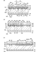
- FIG. 3 is a diagram illustrating an end surface structure taken along lines IIIa-IIIa, IIIb-IIIb, and IIIc-IIIc shown in FIG. 1;
- FIG. 4 is a drawing showing an end face structure taken along line VI-VI shown in FIG. 1.
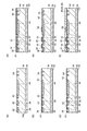
- 2 is a drawing sequentially showing an example of a manufacturing process of the semiconductor device shown in FIG. 1.
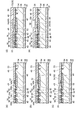
- FIG. 6 is a diagram sequentially illustrating a subsequent process of the process illustrated in FIG. 5.
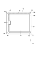
- FIG. 1 is a plan view of a semiconductor device according to an embodiment of the present invention.
- FIG. 2 is a plan view of the semiconductor device when a passivation film provided on the surface side of the semiconductor device shown in FIG. 1 is removed.
- 3A, 3B, and 3C are end views taken along lines IIIa-IIIa, IIIb-IIIb, and IIIc-IIIc in FIG. 1, respectively.
- FIGS. 1 to 3 A schematic configuration of the semiconductor device 10 will be described with reference to FIGS. 1 to 3.
- two directions substantially perpendicular to the thickness direction of the semiconductor device 10 are defined as an x-axis direction and a y-direction. It is called the axial direction.
- the semiconductor device 10 is a MOSFET (Metal-Oxide-Semiconductor-Field-Effect-Transistor) using a compound semiconductor.
- compound semiconductors employed in the semiconductor device 10 include wide band gap semiconductors such as SiC and GaN, and GaAs.
- An example of the shape of the semiconductor device 10 in plan view is a substantially square shape as shown in FIG. Examples of the substantially rectangular shape include a square and a rectangle. When the planar view shape of the semiconductor device 10 is substantially square, an example of the length of one side of the semiconductor device 10 is 5 mm or less.
- the semiconductor device 10 is a semiconductor chip including a cell unit 14 configured by arranging a plurality of unit cells 12 (see FIG. 3A) in parallel.
- the semiconductor device 10 may include an outer peripheral portion 16 (see FIG. 2) that surrounds the cell portion 14 and electrically protects the cell portion 14. In the present embodiment, the semiconductor device 10 including the outer peripheral portion 16 will be described.
- the planar view shape of the cell unit 14 may be the same shape as the planar view shape of the semiconductor device 10. In the present embodiment, as illustrated in FIG. 2, the planar view shape of the cell unit 14 is described as a substantially square shape. An example of the length of one side of the cell portion 14 is 20 ⁇ m or less.
- Each unit cell 12 has a vertical MOSFET structure. As shown in FIG. 3A, adjacent unit cells 12 are physically continuously arranged in parallel.
- the cell portion 14 is an active portion through which a main current flows in the channel region.
- the cell unit 14 may be configured by connecting a plurality of unit cells 12 having a square shape in plan view in parallel in an array. In other embodiments, the unit cell 12 may have a stripe shape extending in one direction. In this case, the cell unit 14 may be configured such that each unit cell 12 has a plurality of unit cells 12 connected in parallel in a direction orthogonal to the extending direction of the unit cells 12.
- the unit cell 12 is partitioned based on the gate electrode 18.
- the source electrode 20 and the drain electrode 22 are shared between the plurality of unit cells 12. Specifically, part of the source electrode 20 and the drain electrode 22 provided on the front surface side and the back surface side of the semiconductor device 10 respectively function as the source electrode and the drain electrode in each unit cell 12. However, the source electrode 20 and the drain electrode 22 may be provided for each unit cell 12.
- a gate electrode wiring 24 is provided along the outer edge portion 14a of the cell portion 14 (an edge portion indicated by a one-dot chain line in FIG. 2). Therefore, the gate electrode wiring 24 is arranged in an annular shape.
- the planar view shape of the cell portion 14 is substantially square, the planar view shape of the gate electrode wiring 24 is also substantially square.
- the gate electrode wiring 24 included in the semiconductor device 10 is electrically connected to the gate electrode 18 of each unit cell 12.
- the gate electrode wiring 24 is a so-called gate runner.
- a first pad electrode 26 (see FIG. 2 and FIG. 3C) is physically connected to a part of the gate electrode wiring 24. Since the gate electrode wiring 24 and the first pad electrode 26 are both conductive, the gate electrode wiring 24 and the first pad electrode 26 are also electrically connected.
- a passivation film 28 (see FIGS. 1, 3A to 3C) as a protective film covering the source electrode 20 and the gate electrode wiring 24 is formed on the surfaces of the cell portion 14 and the outer peripheral portion 16. ing. The surface of the cell portion 14 and the outer peripheral portion 16 is protected by the passivation film 28.
- an opening 28 a and an opening 28 b are formed in the passivation film 28 on the first pad electrode 26 and the source electrode 20, respectively.
- the region of the first pad electrode 26 exposed by the opening 28 a functions as the gate electrode pad 30.
- a region of the source electrode 20 exposed by the opening 28 b functions as the source electrode pad 32.
- the configuration of the semiconductor device 10 will be described in more detail. First, a configuration common to the cell portion 14 and the outer peripheral portion 16 will be described.
- the semiconductor device 10 includes an n-type (first conductivity type) semiconductor substrate 34.
- An example of the material of the semiconductor substrate 34 is a compound semiconductor. Examples of compound semiconductors include wide band gap semiconductors such as SiC and GaN as described above and GaAs.
- An example of the thickness of the semiconductor substrate 34 is 400 ⁇ m.
- a drain electrode 22 is provided on a surface 34 b (hereinafter referred to as a back surface) opposite to the main surface 34 a of the semiconductor substrate 34.
- An example of the drain electrode 22 is a metal film such as a Ni film.
- an n-type drift layer 36 is provided as a base semiconductor layer.
- An example of the material of the drift layer 36 may be the same as the material of the semiconductor substrate 34.
- An example n-type dopant concentration in the drift layer 36 is about 5 ⁇ 10 16 cm ⁇ 3 .
- An example of the thickness of the drift layer 36 is about 10 ⁇ m.
- the configuration of each of the cell part 14 and the outer peripheral part 16 on the semiconductor substrate 34 will be described.
- the cell portion 14 will be described mainly with reference to the configuration on the lower side of the source electrode 20 mainly using FIG.
- the configuration in the vicinity of the outer edge portion 14a of the cell portion 14 will be described later.
- a plurality of p-type (second conductivity type) semiconductor regions 38 as p body regions are formed apart from each other.
- the material of the p-type semiconductor region 38 may be the same as the material of the semiconductor substrate 34.
- An example of the concentration of the p-type dopant in the p-type semiconductor region 38 is about 5 ⁇ 10 17 cm ⁇ 3 .
- An example of the thickness (or depth) of the p-type semiconductor region 38 is about 1.0 ⁇ m.
- n-type source regions 40 are formed apart from each other.
- concentration of the n-type dopant in the source region 40 is about 1 ⁇ 10 19 cm ⁇ 3 .
- An example of the thickness (or depth) of the source region 40 is about 0.3 ⁇ m.
- the gate insulating film 42 and the gate electrode 18 are stacked.
- the gate insulating film 42 and the gate electrode 18 are arranged on a region between adjacent p-type semiconductor regions 38 and 38 so as to form a MOS structure together with the source region 40 in the p-type semiconductor region 38.
- the gate insulating film 42 and the gate electrode 18 can be provided for each unit cell 12.
- An example of the gate insulating film 42 is a silicon oxide film.
- An example of the thickness of the gate insulating film 42 is about 50 ⁇ m.
- An example of the gate electrode 18 is a metal film such as an Al film.
- the raised portion composed of the gate insulating film 42 and the gate electrode 18 is covered with an interlayer insulating film 44.
- An example of the interlayer insulating film 44 is a silicon oxide film.
- a source electrode 20 is provided on the interlayer insulating film 44.
- An example of the source electrode 20 is a metal film such as a Ni film.
- An example of the thickness of the source electrode 20 is about 0.1 ⁇ m.
- a contact region 44 a such as a contact hole penetrating in the thickness direction of the interlayer insulating film 44 is formed in the interlayer insulating film 44 so that the source region 40 and the source electrode 20 are in electrical contact.
- the unit cell 12 has a vertical MOSFET structure and a double diffusion MOSFET structure. Specifically, when the unit cell 12 is viewed from the gate electrode 18, the semiconductor substrate 34, the drain electrode 22 provided on the back surface 34b, the drift layer 36 provided on the main surface 34a, and the surface layer of the drift layer 36 A p-type semiconductor region 38 formed in a portion and spaced apart from each other, a source region 40 formed in each p-type semiconductor region 38, a gate insulating film 42 and a gate electrode 18 forming a MOS structure with the source region 40, and It includes a source electrode 20 electrically connected to the source region 40 and insulated from the gate electrode 18.
- a p-type semiconductor region 38 as a p body region is formed in the surface layer portion of the drift layer 36 along the outer edge portion 14 a of the cell portion 14.
- the p-type semiconductor region 38 formed along the outer edge portion 14 a is also referred to as a p-type semiconductor region 46.
- the p-type semiconductor region 46 projects outward from the cell portion 14 toward the outer peripheral portion 16 side from the cell portion 14 in order to obtain a breakdown voltage characteristic of the semiconductor device 10.
- a source region 40 constituting a part of the unit cell 12 and a source region 40 constituting a MOS structure together with an insulating film 50 and a gate wiring member 52 described later. are spaced apart from each other.
- an insulating film 50 covered with an interlayer insulating film 48 is provided on the p-type semiconductor region 46.
- the materials and thicknesses of the insulating film 50 and the interlayer insulating film 48 may be the same as those of the gate insulating film 42 and the interlayer insulating film 44, respectively.
- a part of the source electrode 20 covers the end of the interlayer insulating film 48 on the center side of the cell portion 14.
- a contact region 48 a penetrating the interlayer insulating film 48 is formed in order to electrically connect the source region 40 and the source electrode 20 in the p-type semiconductor region 46.
- a conductive gate wiring member 52 provided along the outer edge portion 14 a of the cell portion 14 is embedded in the interlayer insulating film 48.
- the thickness and material of the gate wiring member 52 can be the same as those of the gate electrode 18.
- the gate wiring member 52 is electrically connected to each gate electrode 18.
- An example of electrical connection between the gate wiring member 52 and each gate electrode 18 will be described.
- the gate wiring member 52 disposed along the outer edge portion 14a is assumed to be a main gate wiring member (or basic gate wiring member). At this time, a subordinate gate wiring member is led out from the main gate wiring member 52, and the subordinate gate wiring member is stretched in the cell portion 14 so as to be physically connected to each gate electrode 18. Thereby, the gate wiring member 52 and each gate electrode 18 can be electrically connected.
- the subordinate gate wiring member may be covered or buried with an insulating film or the like so as to be insulated from the source electrode 20 and the source region 40.
- both ends of the gate electrode 18 may be physically connected directly to the gate wiring member 52.
- the gate electrode wiring 24 is provided on the interlayer insulating film 48 along the extending direction of the gate wiring member 52, that is, along the outer edge portion 14a. In the interlayer insulating film 48, a contact region 48 b penetrating the interlayer insulating film 48 is formed on the gate electrode wiring 24. The gate electrode wiring 24 is electrically connected to the gate wiring member 52 through the contact region 48b. As a result, the gate electrode wiring 24 is electrically connected to the gate electrode 18 of each unit cell 12.
- the example of the gate electrode wiring 24 may be the same as the example of the source electrode 20.
- the first pad electrode 26 can be formed by forming a part of the gate electrode wiring 24 wide toward the center side of the cell portion 14.
- the p-type semiconductor region 46 and the gate wiring member 52 also project to the center side of the cell portion 14.
- the outer peripheral portion 16 The configuration of the outer peripheral portion 16 will be described with further use of FIG. 3 (b) and FIG. 3 (c).
- the insulating film 50 and the interlayer insulating film 48 are sequentially stacked on the drift layer 36.
- the outer peripheral portion 16 includes the insulating film 50 and the interlayer insulating film 48, but the outer peripheral portion 16 only needs to include the drift layer 36.
- the outer peripheral portion 16 functions as an outer peripheral withstand voltage portion for ensuring the withstand voltage characteristics.
- the p-type semiconductor region 46 can be projected in the region of the outer peripheral portion 16 on the cell portion 14 side.
- the depletion layer at the time of reverse bias is likely to spread more evenly by the p-type semiconductor region 46 protruding in this way. Therefore, it is possible to further ensure the breakdown voltage characteristics in the semiconductor device 10.
- the drift layer 36 included in the outer peripheral portion 16 may be provided with a trench-shaped p-type semiconductor region 54.
- the concentration and thickness of the p-type dopant in the p-type semiconductor region 54 can be the same as in the case of the p-type semiconductor region 38.
- the surfaces of the cell portion 14 and the outer peripheral portion 16 are covered with a passivation film 28.
- An opening 28 a is formed in the passivation film 28 on the first pad electrode 26.
- a region where the first pad electrode 26 is exposed by the opening 28 a is a gate electrode pad 30.
- An opening 28 b is also formed in the passivation film 28 on the source electrode 20.
- the region where the source electrode 20 is exposed by the opening 28 b is the source electrode pad 32.
- An example of the passivation film 28 is a SiN film.
- An example of the thickness of the passivation film 28 is 10 ⁇ m.
- the gate electrode pad 30, the source electrode pad 32, and the drain electrode 22 are externally connected to an element (or circuit) different from the semiconductor device 10, thereby forming each unit constituting the cell unit 14.
- the cell 12 can be electrically connected to an external element (or circuit).
- the semiconductor device 10 has a probe electrode for contacting an inspection probe 56 (see FIG. 4) when the semiconductor device 10 is inspected.
- a pad 58 is provided.
- the semiconductor device 10 may have probe electrode pads 58 at the corners 14 b of the substantially rectangular cell part 14.
- FIG. 1 illustrates a configuration in which probe electrode pads 58 are arranged at four corners 14 b of the cell portion 14. As shown in FIG. 1, the probe electrode pad 58 can protrude from the cell portion 14 toward the outer peripheral portion 16.
- FIG. 4 is an end view schematically showing an end face configuration along line IV-IV in FIG.
- a second pad electrode 60 electrically connected to the gate electrode wiring 24 is provided at the corner of the gate electrode wiring 24. Similar to the first pad electrode 26, the second pad electrode 60 is formed by forming the corner of the gate electrode wiring 24 arranged in a substantially square shape and a region in the vicinity thereof wide. obtain.
- the passivation film 28 further has an opening 28 c on the second pad electrode 60. A region exposed by the opening 28 c in the second pad electrode 60 is a probe electrode pad 58.
- Examples of the planar view shape of the probe electrode pad 58 are a substantially square shape, a substantially fan shape, and a circular shape.
- Examples of the substantially rectangular shape include a substantially rectangular shape and a substantially square shape.
- the size of the probe electrode pad 58 may be a size such that the inspection probe 56 does not contact the peripheral wall of the opening 28 c when the inspection probe 56 is in contact with the probe electrode pad 58. Since the inspection probe 56 does not come into contact with the peripheral wall of the opening 28 c, the area of the surface 58 a of the probe electrode pad 58 or the area of the opening 28 c is the cross-sectional area of the inspection probe 56 and the axis C of the probe 56. Greater than the cross-sectional area perpendicular to each other. In other words, the area of the probe electrode pad 58 is larger than the cross-sectional area of the inspection probe 56 defined based on the diameter D of the inspection probe 56.
- the diameter D is the diameter at the end opposite to the tip of the probe 56. However, when the shape of the tip of the probe 56 is tapered or curved as shown in FIG. 4, the diameter D is equal to the thickness of the passivation film 28 and the other end of the probe 56 from the tip of the probe 56. The diameter at the position close to the side may be sufficient.
- the length of each side defining the probe electrode pad 58 may be 1.1 times or more the diameter D of the probe 56. . If the length of each side defining the probe electrode pad 58 is within the above range, a certain margin (margin) is obtained between the probe 56 and the peripheral wall of the opening 28c. It is hard to touch by. Specifically, as shown in FIG. 1, when the shape of the probe electrode pad 58 is substantially rectangular and the diameter D is 0.027 mm, the short side of the probe electrode pad 58 (IIIc-IIIc in FIG. 1). The length in the direction along the line) may be 0.03 mm or more.
- the diameter of the opening 28c only needs to satisfy the above range.
- the upper limit of the length of the probe electrode pad 58 may be determined according to the size of the outer peripheral portion 16, for example, 1.5 times or less of the diameter D.
- FIGS. 5 (a) to 5 (f) and FIGS. 6 (a) to 6 (e) An example of a method for manufacturing the semiconductor device 10 including the probe electrode pad 58 will be described with reference to FIGS. 5 (a) to 5 (f) and FIGS. 6 (a) to 6 (e). Below, the manufacturing method of the semiconductor device 10 is demonstrated, showing the formation process of the electrode pad 58 for probes concretely.
- 5 (a) to 5 (f) and FIGS. 6 (a) to 6 (e) are drawings sequentially showing manufacturing steps of the semiconductor device 10.
- FIG. 5 (a) to 5 (f) and FIGS. 6 (a) to 6 (e) mainly show the manufacturing process of the semiconductor device 10 in the vicinity of the region where the probe electrode pad 58 is formed. .
- the drift layer 36 is formed on the main surface 34a of the semiconductor substrate 34 made of an n-type SiC substrate, the p-type semiconductor regions 38 and 46 and the source are formed on the surface layer portion of the drift layer 36. Regions 40 are formed respectively.
- the p-type semiconductor region 54 is formed, the p-type semiconductor region 54 is formed together with the p-type semiconductor region 38 and the like. Below, the form provided with the p-type semiconductor region 54 is demonstrated.
- the drift layer 36 is formed on the main surface 34a by using a CVD epitaxial growth method with in-situ doping. When the drift layer 36 is formed using the epitaxial growth method in this way, the drift layer 36 is an epitaxial growth layer.
- the p-type semiconductor regions 38, 46, and 54 are epitaxially grown by a CVD epitaxial growth method with -situ doping.
- the p-type semiconductor region is a buried selective growth region.
- a plurality of source regions 40 are formed in the p-type semiconductor regions 38 and 46 by performing ion implantation using an implantation mask.
- a silicon oxide film 62 as an insulating film is formed on the drift layer 36 by using, for example, a CVD method. Thereafter, the drain electrode 22 made of a Ni film is formed on the back surface 34b by vapor deposition or sputtering.
- the gate insulating film 42 and the insulating film 50 are formed by patterning the silicon oxide film 62, respectively.
- an Al film 64 is formed on the semiconductor substrate 34 by, for example, a CVD method.
- the gate electrode 18 and the gate wiring member 52 are formed as shown in FIG.
- the gate wiring member 52 is formed wide toward the inside of the cell portion.
- a silicon oxide film 66 to be the interlayer insulating films 44 and 48 is further formed on the semiconductor substrate 34 by using, for example, a CVD method.
- the wiring member 52 is embedded.
- the silicon oxide film 66 in order to ensure electrical contact between the source region 40 and the source electrode 20 and electrical contact between the gate wiring member 52 and the gate electrode wiring 24, the silicon oxide film 66.
- Contact regions 44a, 48a, and 48b are formed on the substrate, and interlayer insulating films 44 and 48 are obtained.
- the contact regions 44a, 48a, 48b can be formed using etching or the like.
- a Ni film 68 is formed on the semiconductor substrate 34 having the silicon oxide film 66 (interlayer insulating films 44, 48) in which the contact regions 44a, 48a, 48b are formed by, for example, the CVD method. Film.
- the source electrode 20 and the gate electrode wiring 24 are formed as shown in FIG. 6C.
- the gate electrode wiring 24 is enlarged and formed on the outer peripheral portion 16 side on the corner portion 14 b of the cell portion 14, thereby obtaining the second pad electrode 60.
- the contact between the Ni constituting the source electrode 41 and the drain electrode 22 and the SiC constituting the source region 40 and the semiconductor substrate 34 is changed from a Schottky contact to an ohmic contact. .
- a SiN film 70 is formed on the semiconductor substrate 34 on which the source electrode 20 is formed by, for example, a CVD method.
- This SiN film 70 is the passivation film 28.
- a probe electrode pad 58 is formed as shown in FIG.
- the gate electrode pad 30 and the source electrode pad 32 are formed by forming the openings 28 a and 28 b in the passivation film 28.
- each film has been exemplified, but the materials and the components of the semiconductor device 10 are not limited.
- the method for forming each film is not limited to the exemplified one.
- the semiconductor device 10 described above has a probe electrode pad 58 for inspecting the semiconductor device 10 separately from the gate electrode pad 30.
- the probe electrode pad 58 is electrically connected to the gate electrode 18 and the gate electrode pad 30 through the gate electrode wiring 24. Therefore, the semiconductor device 10 can be inspected by bringing the inspection probe 56 into contact with the probe electrode pad 58 instead of the gate electrode pad 30.
- the gate electrode pad 30 is used not for inspection by the inspection probe but for external connection using wire bonding or the like. be able to. As a result, no extra stress is applied to the gate electrode pad 30 during inspection, and the gate electrode pad 30 can be used in an optimal state during external connection. In addition, since the gate electrode pad 30 is not stressed when the semiconductor device 10 is inspected, the gate electrode pad 30 can be made smaller. Therefore, the current rating of the semiconductor device 10 can be increased.
- the manufacturing time of the semiconductor device 10 can be shortened as compared with the case where the gate electrode pad 30 is made thicker to reduce the influence of stress.
- the probe electrode pad 58 is formed on the outer edge portion 14 a of the cell portion 14. And may be provided so as to project to the outer peripheral portion 16 side. In this case, even if the probe electrode pad 58 is provided separately from the gate electrode pad 30, the area of the cell part 14 as the active part which is the main operation region of the semiconductor device 10 can be maintained. As a result, the operation performance as the semiconductor device 10 can be ensured.
- the region of the outer peripheral portion 16 provided for ensuring the breakdown voltage characteristics is used, it is not necessary to separately secure a region for forming the probe electrode pad 58 so as to protrude outward from the cell portion 14 side.
- the semiconductor device 10 such as a semiconductor chip is desired to have a smaller chip size, and when a compound semiconductor is employed, it is difficult to increase the size because of crystal defects and the like. Therefore, as shown in FIG. 1, the configuration in which the outer peripheral portion 16 is provided and the probe electrode pad 58 is protruded on the outer peripheral portion 16 side is a miniaturization of the semiconductor device 10 (for example, a chip size such that one side of the chip is 5 mm or less). ) And a more effective configuration when a compound semiconductor is employed.
- the planar view shape of the cell portion 14 is, for example, a substantially square shape such as a square, and the gate electrode wiring 24 is disposed along the outer edge portion 14a, the electric field tends to concentrate on the corner portion 14b of the cell portion 14 and the dielectric breakdown occurs. Prone to occur. This is more remarkable in a power MOSFET using SiC, GaN, or the like. Therefore, as shown in FIG. 1, when the outer peripheral portion 16 is provided to ensure the breakdown voltage, the width of the outer peripheral portion 16 of the corner portion 14 b of the cell portion 14 (for example, the outer peripheral portion 16 along the line IIIc-IIIc in FIG. 1). Is wider than the width of the outer peripheral portion 16 at the position of the line IIIb-IIIb shown in FIG. 1, for example.
- the probe electrode pad 58 is disposed on the corner portion 14b of the cell portion 14, and the probe electrode pad 58 is easily spread toward the outer peripheral portion 16 side.
- the probe electrode pad 58 can be formed larger. Therefore, since the contact between the inspection probe 56 and the opening 28c can be more reliably prevented at the time of inspection, the accuracy of inspection of the semiconductor device 10 can be improved.
- the semiconductor device 10 includes two or more (four in FIG. 1) probe electrode pads 58
- the four-terminal method is adopted as the inspection method of the semiconductor device 10. Even in this case, the semiconductor device 10 can be inspected using the two probe electrode pads 58 without using the gate electrode pad 30. Therefore, the semiconductor device 10 can be inspected more accurately without applying stress to the gate electrode pad 30 during the inspection.
- the unit cell 12 of the semiconductor device 10 may have an FET structure. Therefore, the unit cell is not limited to a vertical MOSFET structure, but may be a horizontal MOSFET structure. Further, the unit cell 12 may be a JFET (junction field effect transistor). The FET structure included in the unit cell 12 is not limited to an n-channel type, but may be a p-channel type. Further, the probe electrode pad 58 may be provided separately from the gate electrode pad 18 in the semiconductor device 10 and may be electrically connected to the gate electrode wiring 24. For example, the probe electrode pad 58 may be provided at a position different from the corner portion 14 b of the cell portion 14. Further, the number of probe electrode pads 58 may be 1 to 3, or 5 or more.
- SYMBOLS 10 Semiconductor device, 12 ... Unit cell, 14 ... Cell part, 14a ... Outer edge part, 14b ... Corner
Landscapes
- Electrodes Of Semiconductors (AREA)
- Testing Or Measuring Of Semiconductors Or The Like (AREA)
Abstract
一実施形態に係る半導体装置(10)は、FET構造を有する複数の単位セル(12)を含む半導体装置であって、各単位セルのFET構造が有するゲート電極(18)に電気的に接続されるゲート電極配線(24)と、ゲート電極配線に電気的に接続されており各ゲート電極を外部接続するためのゲート電極パッド(30)と、ゲート電極配線に電気的に接続されており検査用プローブ(56)が接触されるプローブ用電極パッドとを備える。
Description
本発明は半導体装置に関する。
半導体装置として、FET構造(例えば、MOSFET構造)を有する複数の単位セルが並列されたセル部を含む半導体装置が知られている(特許文献1及び非特許文献1参照)。このような半導体装置では、各ゲート電極に導通したゲート電極パッドが設けられており、ゲート電極パッドを外部接続することによって、各単位セルのFET構造に含まれるゲート電極を外部接続している。
稲葉保著、「パワーMOSFET活用の基礎と実際」、CQ出版株式会社、2010年2月1日、第22頁
半導体装置が製造された際には半導体装置の検査が行われる。その検査では、検査用のプローブは、通常、ゲート電極パッドに接触させていた。この場合、検査用のプローブをゲート電極パッドに接触させることによって、本来、外部接続のために使用されるべきゲート電極パッドに余分なストレスが付加されていた。
そこで、本発明は、検査時におけるゲート電極パッドへのストレスを低減し得る半導体装置を提供することを目的とする。
本発明の一側面に係る半導体装置は、FET構造を有する複数の単位セルを含む。この半導体装置は、各単位セルのFET構造が有するゲート電極に電気的に接続されるゲート電極配線と、ゲート電極配線に電気的に接続されており各ゲート電極を外部接続するためのゲート電極パッドと、ゲート電極配線に電気的に接続されており検査用プローブが接触されるプローブ用電極パッドと、を備える。
この形態では、プローブ用電極パッドが、ゲート電極配線を介して各単位セルのゲート電極及びゲート電極パッドに接続されている。よって、ゲート電極パッドの代わりに検査用プローブを接触させることによって、半導体装置を検査し得る。そのため、半導体装置の検査において、ゲート電極パッドへのストレスを低減し得る。
一実施形態に係る半導体装置は、セル部と、セル部を取り囲んでいると共に、セル部を電気的に保護する外周部とを備え得る。この形態において、セル部は、複数の単位セルが並列に配置されて構成され得る。また、プローブ用電極パッドは、セル部の外縁部上に設けられていると共に、セル部から外周部に向けて張り出し得る。
セル部は、FET構造を有する複数の単位セルが並列に配置されて構成されているため、半導体装置において動作領域として機能する。上記形態では、プローブ用電極パッドをゲート電極パッドと別に備えても、動作領域であるセル部の面積(又は大きさ)を確保することが可能である。
一実施形形態では、セル部の平面視形状は略四角形状であり得る。この形態では、ゲート電極配線がセル部の外縁部に沿って配置され得る。また、プローブ用電極パッドは、セル部の外縁部を構成する4つの角部のうちの少なくとも一つの角部の位置に設けられ得る。
セル部の平面視形状が略四角形状であり、セル部の外縁部に沿ってゲート電極配線が配置されている形態では、セル部の角部には電界が集中しやすい。この場合、セル部を取り囲んでいる外周部の幅はより大きくなる傾向にある。よって、セル部の角部にプローブ用電極パッドを配置した形態では、外周部の領域を有効に活用できると共に、プローブ用電極パッドの大きさをより大きくできる。
更に、一実施形態において、プローブ用電極パッドの表面の面積は、検査用プローブの断面であって検査用プローブの軸に直交する断面の面積より大きい。
この形態では、検査用プローブをプローブ用電極パッドに接触させる際、検査用プローブが、半導体装置におけるプローブ用電極パッド以外の領域に接触しにくい。その結果、プローブ用電極パッドを利用して半導体装置をより正確に検査し得る。
一実施形態において、半導体装置は、複数のプローブ用電極パッドを備え得る。この場合、ゲート電極パッドを利用せずに、複数のプローブ用電極パッドに複数の検査用プローブを接触させながら、例えば四端子法を用いて半導体装置を検査し得る。
本発明によれば、検査時におけるゲート電極パッドへのストレスを低減し得る半導体装置を提供し得る。
以下、図面を参照して本発明の実施形態について説明する。図面の説明において、同一要素には同一符号を付し、重複する説明を省略する。図面の寸法比率は、説明のものと必ずしも一致していない。
図1は、本発明の一実施形態に係る半導体装置の平面図である。図2は、図1に示した半導体装置の表面側に設けられるパッシベーション膜を除いた場合の半導体装置の平面図である。図3(a)、図3(b)及び図3(c)は、それぞれ図1のIIIa―IIIa線、IIIb―IIIb線及びIIIc-IIIc線に沿った端面図である。
図1~図3を利用して半導体装置10の概略構成について説明する。説明のために、図1及び図2に示すように、半導体装置10の厚さ方向(後述する半導体基板34の主面34aの法線方向)に略直交する2つの方向をx軸方向及びy軸方向と称す。
半導体装置10は、化合物半導体を利用したMOSFET(Metal-Oxide-Semiconductor Field-Effect Transistor)である。半導体装置10に採用される化合物半導体の例は、SiC及びGaNといったワイドバンドギャップ半導体、GaAsを含む。半導体装置10は平面視形状(半導体装置10の厚さ方向から見た形状)の例は、図1に示されているような略四角形状である。略四角形状の例は、正方形及び長方形を含む。半導体装置10の平面視形状が略正方形である場合において、半導体装置10の一辺の長さの例は5mm以下である。
半導体装置10は、複数の単位セル12(図3(a)参照)が並列に配置されて構成されるセル部14を備えた半導体チップである。半導体装置10は、セル部14を取り囲んでおりセル部14を電気的に保護する外周部16(図2参照)を備え得る。本実施形態では、外周部16を備えた半導体装置10が説明される。
セル部14の平面視形状は、半導体装置10の平面視形状と同様の形状であり得る。本実施形態では、図2に例示したように、セル部14の平面視形状は略正方形として説明される。セル部14の一辺の長さの例は20μm以下である。
各単位セル12は縦型のMOSFET構造を有する。図3(a)に示すように、隣接する単位セル12は物理的に連続して並列配置されている。この形態では、セル部14はチャネル領域に主電流が流れる活性部である。一実施形態において、セル部14は、平面視形状が角状の複数の単位セル12がアレイ状に並列接続されて構成され得る。他の実施形態において、単位セル12は、一方向に延在したストライプ形状を有し得る。この場合には、セル部14は、各単位セル12が単位セル12の延在方向に直交する方向に複数の単位セル12が並列接続された構成とし得る。
単位セル12は、ゲート電極18を基準にして区画されている。半導体装置10では、複数の単位セル12間において、ソース電極20及びドレイン電極22が共有されている。具体的には、半導体装置10の表面側及び裏面側にそれぞれ設けられたソース電極20及びドレイン電極22の一部が各単位セル12におけるソース電極及びドレイン電極として機能する。ただし、単位セル12毎に、ソース電極20及びドレイン電極22がそれぞれ設けられてもよい。
セル部14の表面には、ゲート電極配線24がセル部14の外縁部14a(図2において一点鎖線で示される縁部)に沿って設けられている。よって、ゲート電極配線24は、環状に配置されている。本実施形態ではセル部14の平面視形状は略正方形であるため、ゲート電極配線24の平面視形状も略正方形である。半導体装置10が有するゲート電極配線24は、各単位セル12のゲート電極18に電気的に接続されている。ゲート電極配線24は、いわゆるゲートランナーである。ゲート電極配線24の一部には、第1のパッド用電極26(図2、図3(c)参照)が物理的に接続されている。ゲート電極配線24及び第1のパッド用電極26はいずれも導電性を有することから、ゲート電極配線24及び第1のパッド用電極26は電気的にも接続されている。
セル部14及び外周部16の表面上には、ソース電極20及ゲート電極配線24を覆う保護膜としてのパッシベーション膜28(図1、図3(a)~図3(c)参照)が形成されている。このパッシベーション膜28によりセル部14及び外周部16の表面が保護される。半導体装置10では、第1のパッド用電極26及びソース電極20上のパッシベーション膜28に開口部28a及び開口部28bがそれぞれ形成されている。開口部28aによって露出した第1のパッド用電極26の領域がゲート電極パッド30として機能する。同様に、ソース電極20のうち開口部28bによって露出された領域がソース電極パッド32として機能する。
図3(a)~図3(c)を利用して、半導体装置10の構成について更に詳細に説明する。まず、セル部14及び外周部16に共通の構成について説明する。
半導体装置10は、n型(第1導電型)の半導体基板34を有する。半導体基板34の材料の例は化合物半導体である。化合物半導体の例は、前述したSiC及びGaNといったワイドバンドギャップ半導体並びにGaAsを含む。半導体基板34の厚さの例は400μmである。半導体基板34の主面34aと反対側の面34b(以下、裏面と称す)には、ドレイン電極22が設けられている。ドレイン電極22の例はNi膜といった金属膜である。半導体基板34の主面34a上には、下地半導体層としてn型のドリフト層36が設けられている。ドリフト層36の材料の例は半導体基板34の材料と同じとし得る。ドリフト層36内のn型ドーパントの濃度の例は約5×1016cm-3である。ドリフト層36の厚さの例は約10μmである。
次に、半導体基板34上のセル部14及び外周部16それぞれの構成について説明する。まず、セル部14について、図3(a)を主に利用してソース電極20の下側の構成を中心にして説明する。セル部14の外縁部14a近傍の構成については後述する。
ドリフト層36の表層部には、pボディ領域としての複数のp型(第2導電型)半導体領域38が互いに離間して形成されている。p型半導体領域38の材料は半導体基板34の材料と同じとし得る。p型半導体領域38のp型ドーパントの濃度の例は約5×1017cm-3である。p型半導体領域38の厚さ(又は深さ)の例は約1.0μmである。単位セル12の平面視形状が角状である場合には、p型半導体領域38はドリフト層36の表層部に島状に形成され得る。一方、単位セル12が一方向に延在している場合には、p型半導体領域38も一方向に延在し得る。
p型半導体領域38には、2つのn型のソース領域40が離間して形成されている。ソース領域40内のn型のドーパントの濃度の例は約1×1019cm-3である。ソース領域40の厚み(又は深さ)の例は約0.3μmである。
ドリフト層36の表面において隣接するp型半導体領域38,38の間の領域上には、ゲート絶縁膜42及びゲート電極18が積層されている。ゲート絶縁膜42及びゲート電極18は、p型半導体領域38内のソース領域40と共にMOS構造を形成するように、隣接するp型半導体領域38,38の間の領域上に配置されている。本実施形態では、ゲート絶縁膜42及びゲート電極18は、単位セル12毎に設けられ得る。ゲート絶縁膜42の例はシリコン酸化膜である。ゲート絶縁膜42の厚さの例は約50μmである。ゲート電極18の例はAl膜といった金属膜である。
ゲート絶縁膜42及びゲート電極18からなる隆起部は、層間絶縁膜44によって被覆されている。層間絶縁膜44の例はシリコン酸化膜である。層間絶縁膜44上には、ソース電極20が設けられている。ソース電極20の例はNi膜といった金属膜である。ソース電極20の厚さの例は約0.1μmである。ソース領域40とソース電極20とが電気的に接触するように層間絶縁膜44には、層間絶縁膜44の厚さ方向に貫通するコンタクトホールといったコンタクト領域44aが形成されている。
上記構成では、単位セル12は、縦型MOSFET構造であって二重拡散型MOSFET構造を有する。具体的には、単位セル12は、ゲート電極18を基準としてみた場合、半導体基板34、裏面34bに設けられたドレイン電極22、主面34a上に設けられたドリフト層36、ドリフト層36の表層部に形成されており互いに離間したp型半導体領域38、各p型半導体領域38内に形成されたソース領域40、ソース領域40とMOS構造を形成するゲート絶縁膜42及びゲート電極18、並びに、ソース領域40と電気的に接続されゲート電極18と絶縁されたソース電極20とを含む。
次に、図3(b)及び図3(c)を主に利用して、ゲート電極配線24が形成されるセル部14の外縁部14aの構成について説明する。
セル部14の外縁部14aに沿ってpボディ領域としてのp型半導体領域38がドリフト層36の表層部に形成されている。以下、説明の便宜のため、外縁部14aに沿って形成されるp型半導体領域38をp型半導体領域46とも称す。一実施形態において、p型半導体領域46は、半導体装置10の耐圧特性を得るために、セル部14から外周部16側に向けてセル部14から外側に張り出している。p型半導体領域46のセル部14中心側の端部には、単位セル12の一部を構成するソース領域40と、後述する絶縁膜50及びゲート配線部材52と共にMOS構造を構成するソース領域40とが互いに離間して形成されている。
p型半導体領域46上には層間絶縁膜48によって被覆された絶縁膜50が設けられている。絶縁膜50及び層間絶縁膜48の材料及び厚さは、それぞれゲート絶縁膜42及び層間絶縁膜44の場合と同じとし得る。層間絶縁膜48のセル部14の中心側の端部上には、ソース電極20の一部が被さっている。層間絶縁膜48には、p型半導体領域46内のソース領域40とソース電極20とを電気的に接続するために、層間絶縁膜48を貫通するコンタクト領域48aが形成されている。
層間絶縁膜48内には、セル部14の外縁部14aに沿って設けられた導電性のゲート配線部材52が埋設されている。ゲート配線部材52の厚さ及び材料は、ゲート電極18の場合と同様とし得る。ゲート配線部材52は、各ゲート電極18と電気的に接続されている。ゲート配線部材52と各ゲート電極18との電気的な接続の例について説明する。外縁部14aに沿って配置されたゲート配線部材52を主たるゲート配線部材(又は基幹ゲート配線部材)とする。この際、主たるゲート配線部材52から従たるゲート配線部材を導出して、この従たるゲート配線部材を各ゲート電極18と物理的に接続されるようにセル部14内に張り巡らせる。これにより、ゲート配線部材52と各ゲート電極18とが電気的に接続され得る。この場合、従たるゲート配線部材は、ソース電極20及びソース領域40とは絶縁されるように絶縁膜などによって被覆又は埋設されていればよい。或いは、単位セル12が一方向に延在している形態では、ゲート電極18の両端を直接ゲート配線部材52に物理的に接続してもよい。
ゲート配線部材52の延びている方向、すなわち、外縁部14aに沿って層間絶縁膜48上にゲート電極配線24が設けられている。層間絶縁膜48には、ゲート電極配線24上に層間絶縁膜48を貫通するコンタクト領域48bが形成されている。コンタクト領域48bを介してゲート電極配線24は、ゲート配線部材52と電気的に接続される。その結果、ゲート電極配線24は、各単位セル12のゲート電極18と電気的に接続される。ゲート電極配線24の例はソース電極20の例と同じとし得る。
ゲート電極配線24の一部、例えば、図1に示すように、略四角形状に配設されたゲート電極配線24のうちy軸方向に延在している領域の一部には、図3(c)に示すように、第1のパッド用電極26が設けられている。ゲート電極配線24の一部をセル部14の中心側に向けて幅広に形成することによって第1のパッド用電極26を形成し得る。第1のパッド用電極26の下側においては、p型半導体領域46及びゲート配線部材52もセル部14の中心側に張り出している。
図3(b)及び図3(c)を更に利用して、外周部16の構成について説明する。外周部16では、ドリフト層36上に、絶縁膜50及び層間絶縁膜48が順に積層されている。ここでは、外周部16は、絶縁膜50及び層間絶縁膜48を含んでいるとしたが、外周部16は、ドリフト層36を備えていればよい。セル部14と共通のドリフト層36を備えることで、逆バイアス時の空乏層がより広がりやすく、耐圧特性を得ることができる。この場合、外周部16は、耐圧特性を確保するための外周耐圧部として機能する。
外周部16のセル部14側の領域には、前述したように、p型半導体領域46が張り出され得る。このように張り出されたp型半導体領域46によって逆バイアス時の空乏層が更に均等に広がり易い。そのため、半導体装置10における耐圧特性をより確保可能である。また、耐圧特性を更に確保するために、外周部16が有するドリフト層36には、トレンチ状のp型半導体領域54が設けられていてもよい。p型半導体領域54のp型ドーパントの濃度及び厚さは、p型半導体領域38の場合と同様とし得る。
図3(a)~図3(c)に示すように、セル部14及び外周部16の表面は、パッシベーション膜28で覆われている。第1のパッド用電極26上のパッシベーション膜28に開口部28aが形成されている。開口部28aによって第1のパッド用電極26の露出した領域がゲート電極パッド30である。ソース電極20上のパッシベーション膜28にも開口部28bが形成されている。開口部28bによって、ソース電極20の露出した領域がソース電極パッド32である。パッシベーション膜28の例はSiN膜である。パッシベーション膜28の厚さの例は、10μmである。
上記構成の半導体装置10では、ゲート電極パッド30、ソース電極パッド32及びドレイン電極22を、半導体装置10とは別の素子(又は回路)に外部接続することによって、セル部14を構成する各単位セル12が外部の素子(又は回路)に電気的に接続され得る。
半導体装置10は、図1に示すように、上記ゲート電極パッド30及びソース電極パッド32に加えて、半導体装置10の検査時に、検査用プローブ56(図4参照)を接触させるためのプローブ用電極パッド58を備える。一実施形態において、図1及び図2に示されているように、半導体装置10は、略四角形状のセル部14の角部14bにプローブ用電極パッド58を有し得る。図1では、セル部14の4つの角部14bにプローブ用電極パッド58が配置された構成を例示している。プローブ用電極パッド58は、図1に示すように、セル部14から外周部16に向けて張り出し得る。
図4を利用してプローブ用電極パッド58の形成位置における半導体装置10の構成について更に説明する。図4は、図1のIV―IV線に沿った端面構成を模式的に示す端面図である。
層間絶縁膜48上において、ゲート電極配線24の角部に、ゲート電極配線24に電気的に接続された第2のパッド用電極60が設けられている。第1のパッド用電極26と同様に、略四角形状に配設されたゲート電極配線24の角部及びその近傍の領域が幅広に形成されることによって、第2のパッド用電極60を形成し得る。パッシベーション膜28は、第2のパッド用電極60上に、開口部28cを更に有する。第2のパッド用電極60のうち開口部28cによって露出した領域がプローブ用電極パッド58である。
プローブ用電極パッド58の平面視形状の例は、略四角形、略扇形状及び円状である。略四角形の例は、略長方形及び略正方形を含む。プローブ用電極パッド58の大きさは、検査用プローブ56がプローブ用電極パッド58に接触される場合に、検査用プローブ56が開口部28cの周壁に接触しない大きさであり得る。検査用プローブ56が開口部28cの周壁に接触しないために、プローブ用電極パッド58の表面58aの面積又は開口部28cの面積は、検査用プローブ56の断面積であってプローブ56の軸Cに直交する断面の面積より大きい。換言すれば、プローブ用電極パッド58の面積は、検査用プローブ56の径Dに基づいて規定される検査用プローブ56の断面積より大きい。
径Dは、プローブ56の先端部と反対側の端部における径である。しかしながら、プローブ56の先端部の形状が図4に示すように先細りしたテーパ形状或いは湾曲形状である場合、径Dは、パッシベーション膜28の厚さ分、プローブ56の先端部からプローブ56の他端側に寄った位置での径であればよい。
検査用プローブ56が開口部28cの周壁に接触しないために、一実施形態において、プローブ用電極パッド58を規定する各辺の長さは、プローブ56の径Dの1.1倍以上であり得る。プローブ用電極パッド58を規定する各辺の長さが上記範囲であれば、プローブ56と開口部28cの周壁との間に、一定の余白(マージン)が得られるので、プローブ56が開口部28cにより接触しにくい。具体的には、図1に示すように、プローブ用電極パッド58の形状が略長方形であり、径Dが0.027mmである場合、プローブ用電極パッド58の短辺(図1のIIIc-IIIc線に沿った方向の長さ)は0.03mm以上とし得る。開口部28cがプローブ用電極パッド58の形状が円形である場合には、開口部28cの直径が上記範囲を満たせばよい。プローブ用電極パッド58の長さの上限は外周部16の大きさに応じて決めればよいが、例えば径Dの1.5倍以下である。
プローブ用電極パッド58を含む半導体装置10の製造方法の一例を、図5(a)~図5(f)及び図6(a)~図6(e)を利用して説明する。以下では、プローブ用電極パッド58の形成工程を具体的に示しながら半導体装置10の製造方法を説明する。図5(a)~図5(f)及び図6(a)~図6(e)は、半導体装置10の製造工程を順次示す図面である。図5(a)~図5(f)及び図6(a)~図6(e)では、プローブ用電極パッド58が形成される領域近傍の半導体装置10の製造工程が主に示されている。
図5(a)に示すように、n型のSiC基板からなる半導体基板34の主面34a上にドリフト層36を形成した後、ドリフト層36の表層部にp型半導体領域38,46及びソース領域40をそれぞれ形成する。p型半導体領域54を形成する場合には、p型半導体領域38等と一緒にp型半導体領域54を形成する。以下では、p型半導体領域54を備えた形態が説明される。具体的には、主面34a上に、in-situドープを伴うCVDエピタキシャル成長法を用いてドリフト層36を形成する。このようにエピタキシャル成長法を利用してドリフト層36が形成される場合、ドリフト層36はエピタキシャル成長層である。ドリフト層36の所定位置にRIE(Reactive Ion Etching)(反応性イオンエッチング)などにより、p型半導体領域38,46,54となる凹部を形成した後、各凹部の底面及び側面の上に、in-situドープを伴うCVDエピタキシャル成長法によってp型半導体領域38,46,54をエピタキシャル成長させる。この場合、p型半導体領域は埋込選択成長領域である。p型半導体領域38,46に、注入マスクを用いたイオン注入を実施することによって、複数のソース領域40を形成する。
次いで、図5(b)に示すように、ドリフト層36上に、例えばCVD法を用いて絶縁膜としてのシリコン酸化膜62を成膜する。その後、蒸着法又はスパッタ法などによって、裏面34b上にNi膜からなるドレイン電極22を形成する。
次に、図5(c)に示すように、シリコン酸化膜62をパターニングすることによって、ゲート絶縁膜42及び絶縁膜50をそれぞれ形成する。続いて、図5(d)に示すように、半導体基板34上に、例えばCVD法などによってAl膜64を形成する。そのAl膜64をパターニングすることによって、図5(e)に示すように、ゲート電極18及びゲート配線部材52を形成する。第1のパッド用電極26の直下に位置する領域においては、図3(c)に示したように、ゲート配線部材52を、セル部14の内側に向けて幅広に形成する。その後、図5(f)に示すように、半導体基板34上に更に、例えばCVD法を用いて、層間絶縁膜44,48となるシリコン酸化膜66を成膜することによって、ゲート電極18及びゲート配線部材52を埋設する。
続いて、図6(a)に示すように、ソース領域40とソース電極20との電気的接触及びゲート配線部材52とゲート電極配線24との電気的接触を確保するために、シリコン酸化膜66にコンタクト領域44a,48a,48bを形成し、層間絶縁膜44,48を得る。コンタクト領域44a,48a,48bは、エッチングなどを利用して形成され得る。
図6(b)に示すように、コンタクト領域44a,48a,48bが形成されたシリコン酸化膜66(層間絶縁膜44,48)を有する半導体基板34上に、例えばCVD法によってNi膜68を成膜する。そのNi膜68をパターニングすることによって、図6(c)に示すように、ソース電極20及びゲート電極配線24を形成する。この際、セル部14の角部14b上において、ゲート電極配線24を外周部16側に拡大して形成することによって、第2のパッド用電極60を得る。ここで、半導体基板34を、熱処理することによって、ソース電極41及びドレイン電極22を構成するNiと、ソース領域40及び半導体基板34を構成するSiCとの接触をショットキー接触からオーミック接触に変化させる。
図6(d)に示すように、ソース電極20が形成された半導体基板34上にSiN膜70を例えばCVD法などにより形成する。このSiN膜70がパッシベーション膜28である。このパッシベーション膜28に、エッチング等を利用して開口部28cを形成することによって、図6(e)に示すように、プローブ用電極パッド58を形成する。この際、パッシベーション膜28に開口部28a,28bを形成することによって、ゲート電極パッド30及びソース電極パッド32を形成する。
ここでは、半導体基板34、ゲート電極18、ソース電極20及びドレイン電極22などの材料及び各膜の形成方法などを一部例示しながら説明したが、半導体装置10を構成する各構成要素の材料及び各膜の形成方法などは例示したものに限定されない。
以上説明した半導体装置10は、ゲート電極パッド30とは別に、半導体装置10の検査のためのプローブ用電極パッド58を有する。プローブ用電極パッド58はゲート電極配線24を介してゲート電極18及びゲート電極パッド30に電気的に接続されている。そのため、ゲート電極パッド30ではなく、プローブ用電極パッド58に検査用プローブ56を接触させることによって、半導体装置10を検査することができる。
このように、プローブ用電極パッド58を利用して半導体装置10を検査することにより、ゲート電極パッド30を検査用プローブによる検査のためではなく、ワイヤボンディングなどを利用した外部接続のために使用することができる。その結果、検査時においてゲート電極パッド30に余分なストレスが付加されることがなく、外部接続時にゲート電極パッド30を最適な状態で使用し得る。また、半導体装置10の検査時にゲート電極パッド30にストレスがかからないので、ゲート電極パッド30をより小さく形成し得る。そのため、半導体装置10の電流定格を上げることができる。
また、検査時におけるゲート電極パッド30へのストレスを考慮する必要がないので、ストレスの影響を低下するために、ゲート電極パッド30やゲート電極18の厚さをより厚く形成する必要がない。その結果、ゲート電極パッド30をより厚くしてストレスの影響の低下を図る場合よりも、半導体装置10の製造時間を短縮することも可能である。
図1に例示したように、耐圧特性を確保するため、半導体装置10がセル部14を囲繞する外周部16を備えている形態では、プローブ用電極パッド58は、セル部14の外縁部14a上に配置されると共に、外周部16側に張り出すように設けられ得る。この場合、ゲート電極パッド30とは別にプローブ用電極パッド58を備えたとしても、半導体装置10の主動作領域である活性部としてのセル部14の面積を維持できる。結果として、半導体装置10としての動作性能を確保し得る。また、耐圧特性の確保のために備える外周部16の領域を利用しているため、プローブ用電極パッド58をセル部14側から外側に張り出して形成するための領域を別途確保する必要がない。近年、半導体チップといった半導体装置10はチップサイズの小型化が望まれていると共に、化合物半導体を採用している場合には、結晶欠陥などの関係から大型化が困難である。そのため、図1に示したように、外周部16を備え、外周部16側にプローブ用電極パッド58を張り出した形態は、半導体装置10の小型化(例えば、チップの一辺が5mm以下といったチップサイズ)に資する構成であると共に、化合物半導体を採用した場合により有効な構成である。
セル部14の平面視形状が例えば正方形といった略四角形状であって外縁部14aに沿ってゲート電極配線24が配置された場合、セル部14の角部14bには電界が集中しやすく絶縁破壊が生じやすい。これは、SiC又はGaN等を利用したパワーMOSFETにおいてより顕著である。そのため、図1に示したように、耐圧確保のために外周部16を備える場合、セル部14の角部14bの外周部16の幅(例えば図1のIIIc―IIIc線に沿った外周部16の幅)は、例えば、図1に示したIIIb―IIIb線の位置の外周部16の幅より広くなっている。その結果、セル部14の角部14bにプローブ用電極パッド58を配置し、プローブ用電極パッド58を外周部16側に広げ易い。この形態では、上記のように、外周部16においてより広い領域を利用していることから、プローブ用電極パッド58をより大きく形成し得る。従って、検査時に検査用プローブ56と開口部28cとの接触をより確実に防止できるので、半導体装置10の検査の精度向上を図ることができる。
また、図1に示したように、半導体装置10が2つ以上(図1では4個)のプローブ用電極パッド58を備えている形態では、半導体装置10の検査方法として四端子法を採用した場合であっても、ゲート電極パッド30を使用せずに、2つのプローブ用電極パッド58を利用して半導体装置10を検査可能である。よって、検査時に、ゲート電極パッド30にストレスをかけずに、半導体装置10をより精度よく検査し得る。
以上、本発明の実施形態について説明したが、本発明は上記実施形態に限定されずに、本発明の趣旨を逸脱しない範囲で種々変形が可能である。例えば、半導体装置10の単位セル12は、FET構造を有してればよい。よって、単位セルは、MOSFET構造は縦型のMOSFET構造に限らず、横型のMOSFET構造であってもよい。更に、単位セル12は、JFET(接合型電界効果トランジスタ)であってもよい。単位セル12が有するFET構造は、nチャネル型のものに限らず、pチャネル型であり得る。更に、プローブ用電極パッド58は、半導体装置10においてゲート電極パッド18とは別に設けられており、ゲート電極配線24に電気的に接続されていればよい。例えば、プローブ用電極パッド58は、セル部14の角部14bとは異なる位置に設けられていてもよい。更に、プローブ用電極パッド58の個数は1個~3個でもよく、5個以上でもよい。
10…半導体装置、12…単位セル、14…セル部、14a…外縁部、14b…角部、16…外周部、18…ゲート電極、24…ゲート電極配線、30…ゲート電極パッド、56…検査用プローブ、58…プローブ用電極パッド。
Claims (5)
- FET構造を有する複数の単位セルを含む半導体装置において、
各前記単位セルの前記FET構造が有するゲート電極に電気的に接続されるゲート電極配線と、
前記ゲート電極配線に電気的に接続されており各前記ゲート電極を外部接続するためのゲート電極パッドと、
前記ゲート電極配線に電気的に接続されており検査用プローブが接触されるプローブ用電極パッドと、
を備える半導体装置。 - セル部と、
前記セル部を取り囲んでいると共に、前記セル部を電気的に保護する外周部と、
を備え、
前記セル部は、複数の前記単位セルが並列に配置されて構成されており、
前記プローブ用電極パッドは、前記セル部の外縁部上に設けられていると共に、前記セル部から前記外周部に向けて張り出している、
請求項1記載の半導体装置。 - 前記セル部の平面視形状は略四角形状であり、
前記ゲート電極配線は、前記セル部の外縁部に沿って配置されており、
前記プローブ用電極パッドは、前記セル部の4つの角部のうちの少なくとも一つの角部に設けられている、
請求項2記載の半導体装置。 - 前記プローブ用電極パッドの表面の面積は、前記検査用プローブの断面であって前記検査用プローブの軸に直交する前記断面の面積より大きい、請求項1~3の何れか一項記載の半導体装置。
- 複数の前記プローブ用電極パッドを備える、請求項1~4の何れか一項記載の半導体装置。
Applications Claiming Priority (2)
| Application Number | Priority Date | Filing Date | Title |
|---|---|---|---|
| JP2011-115652 | 2011-05-24 | ||
| JP2011115652A JP5655705B2 (ja) | 2011-05-24 | 2011-05-24 | 半導体装置 |
Publications (1)
| Publication Number | Publication Date |
|---|---|
| WO2012160868A1 true WO2012160868A1 (ja) | 2012-11-29 |
Family
ID=47216957
Family Applications (1)
| Application Number | Title | Priority Date | Filing Date |
|---|---|---|---|
| PCT/JP2012/057052 Ceased WO2012160868A1 (ja) | 2011-05-24 | 2012-03-19 | 半導体装置 |
Country Status (3)
| Country | Link |
|---|---|
| US (1) | US20120298994A1 (ja) |
| JP (1) | JP5655705B2 (ja) |
| WO (1) | WO2012160868A1 (ja) |
Cited By (1)
| Publication number | Priority date | Publication date | Assignee | Title |
|---|---|---|---|---|
| JP2016152299A (ja) * | 2015-02-17 | 2016-08-22 | 三菱電機株式会社 | 半導体装置および半導体モジュール |
Families Citing this family (7)
| Publication number | Priority date | Publication date | Assignee | Title |
|---|---|---|---|---|
| US9379048B2 (en) * | 2013-02-28 | 2016-06-28 | Semiconductor Components Industries, Llc | Dual-flag stacked die package |
| JP6058228B1 (ja) * | 2015-04-22 | 2017-01-11 | 三菱電機株式会社 | 半導体装置および半導体装置の製造方法 |
| JP6641488B2 (ja) * | 2016-08-25 | 2020-02-05 | 三菱電機株式会社 | 半導体装置 |
| JP2019145646A (ja) * | 2018-02-20 | 2019-08-29 | 株式会社東芝 | 半導体装置 |
| JP7200488B2 (ja) * | 2018-03-19 | 2023-01-10 | 富士電機株式会社 | 絶縁ゲート型半導体装置 |
| JP7275572B2 (ja) * | 2018-12-27 | 2023-05-18 | 富士電機株式会社 | 半導体装置および半導体装置の製造方法 |
| JP7729033B2 (ja) * | 2020-11-24 | 2025-08-26 | 富士電機株式会社 | 炭化珪素半導体装置、半導体パッケージおよび炭化珪素半導体装置の検査方法 |
Citations (4)
| Publication number | Priority date | Publication date | Assignee | Title |
|---|---|---|---|---|
| JPH08162537A (ja) * | 1994-12-07 | 1996-06-21 | Hitachi Ltd | 半導体装置 |
| JPH11177087A (ja) * | 1997-12-09 | 1999-07-02 | Hitachi Ltd | 半導体集積回路装置の製造方法および半導体集積回路装置 |
| JP2004055812A (ja) * | 2002-07-19 | 2004-02-19 | Renesas Technology Corp | 半導体装置 |
| JP2006184136A (ja) * | 2004-12-28 | 2006-07-13 | Aitesu:Kk | 半導体解析装置およびその方法 |
Family Cites Families (4)
| Publication number | Priority date | Publication date | Assignee | Title |
|---|---|---|---|---|
| JP4142029B2 (ja) * | 2004-05-07 | 2008-08-27 | セイコーエプソン株式会社 | 電気光学装置および電子機器 |
| WO2009141347A1 (de) * | 2008-05-19 | 2009-11-26 | X-Fab Semiconductor Foundries Ag | Betriebstemperaturmessung eines mos-leistungsbauelements und mos bauelement zur ausfuehrung des verfahrens |
| US8017942B2 (en) * | 2008-11-25 | 2011-09-13 | Infineon Technologies Ag | Semiconductor device and method |
| JP5486866B2 (ja) * | 2009-07-29 | 2014-05-07 | ルネサスエレクトロニクス株式会社 | 半導体装置の製造方法 |
-
2011
- 2011-05-24 JP JP2011115652A patent/JP5655705B2/ja not_active Expired - Fee Related
-
2012
- 2012-03-19 WO PCT/JP2012/057052 patent/WO2012160868A1/ja not_active Ceased
- 2012-05-22 US US13/477,855 patent/US20120298994A1/en not_active Abandoned
Patent Citations (4)
| Publication number | Priority date | Publication date | Assignee | Title |
|---|---|---|---|---|
| JPH08162537A (ja) * | 1994-12-07 | 1996-06-21 | Hitachi Ltd | 半導体装置 |
| JPH11177087A (ja) * | 1997-12-09 | 1999-07-02 | Hitachi Ltd | 半導体集積回路装置の製造方法および半導体集積回路装置 |
| JP2004055812A (ja) * | 2002-07-19 | 2004-02-19 | Renesas Technology Corp | 半導体装置 |
| JP2006184136A (ja) * | 2004-12-28 | 2006-07-13 | Aitesu:Kk | 半導体解析装置およびその方法 |
Cited By (1)
| Publication number | Priority date | Publication date | Assignee | Title |
|---|---|---|---|---|
| JP2016152299A (ja) * | 2015-02-17 | 2016-08-22 | 三菱電機株式会社 | 半導体装置および半導体モジュール |
Also Published As
| Publication number | Publication date |
|---|---|
| JP5655705B2 (ja) | 2015-01-21 |
| US20120298994A1 (en) | 2012-11-29 |
| JP2012244102A (ja) | 2012-12-10 |
Similar Documents
| Publication | Publication Date | Title |
|---|---|---|
| JP5655705B2 (ja) | 半導体装置 | |
| JP4892172B2 (ja) | 半導体装置およびその製造方法 | |
| US8541834B2 (en) | Semiconductor device and method for manufacturing same | |
| US10396149B2 (en) | Semiconductor device and method of manufacturing semiconductor device | |
| US9748393B2 (en) | Silicon carbide semiconductor device with a trench | |
| WO2011021413A1 (ja) | 半導体装置 | |
| JP2019071313A (ja) | 半導体装置 | |
| US11489071B2 (en) | Semiconductor device | |
| US10833185B2 (en) | Heterojunction semiconductor device having source and drain pads with improved current crowding | |
| US9035320B2 (en) | Semiconductor device | |
| JP7351086B2 (ja) | 絶縁ゲート型半導体装置及びその製造方法 | |
| US9257501B2 (en) | Semiconductor device | |
| US11049964B2 (en) | Silicon carbide semiconductor device | |
| JP5324157B2 (ja) | 半導体装置およびその製造方法 | |
| JP5957171B2 (ja) | 半導体装置及びその製造方法 | |
| JP7680503B2 (ja) | 縦型電界効果トランジスタおよびその形成のための方法 | |
| US20080093638A1 (en) | Semiconductor Device | |
| CN106449751A (zh) | 半导体装置及其制造方法 | |
| US12501652B2 (en) | Semiconductor device | |
| JP2024107477A (ja) | 電界効果トランジスタ | |
| US12002892B2 (en) | Semiconductor device with embedded Schottky diode and manufacturing method thereof | |
| US10418477B2 (en) | Silicon carbide semiconductor device and method of manufacturing silicon carbide semiconductor device | |
| GB2563110A (en) | Silicon carbide semiconductor device and manufacturing method thereof | |
| JP2021129020A (ja) | 半導体装置 | |
| JP7628874B2 (ja) | 半導体装置及びその製造方法 |
Legal Events
| Date | Code | Title | Description |
|---|---|---|---|
| 121 | Ep: the epo has been informed by wipo that ep was designated in this application |
Ref document number: 12788940 Country of ref document: EP Kind code of ref document: A1 |
|
| NENP | Non-entry into the national phase |
Ref country code: DE |
|
| 122 | Ep: pct application non-entry in european phase |
Ref document number: 12788940 Country of ref document: EP Kind code of ref document: A1 |