WO2012147725A1 - 半導体チップのピックアップ装置 - Google Patents
半導体チップのピックアップ装置 Download PDFInfo
- Publication number
- WO2012147725A1 WO2012147725A1 PCT/JP2012/060937 JP2012060937W WO2012147725A1 WO 2012147725 A1 WO2012147725 A1 WO 2012147725A1 JP 2012060937 W JP2012060937 W JP 2012060937W WO 2012147725 A1 WO2012147725 A1 WO 2012147725A1
- Authority
- WO
- WIPO (PCT)
- Prior art keywords
- claw
- semiconductor chip
- housing
- tip
- adhesive sheet
- Prior art date
- Legal status (The legal status is an assumption and is not a legal conclusion. Google has not performed a legal analysis and makes no representation as to the accuracy of the status listed.)
- Ceased
Links
Images




Classifications
-
- H—ELECTRICITY
- H10—SEMICONDUCTOR DEVICES; ELECTRIC SOLID-STATE DEVICES NOT OTHERWISE PROVIDED FOR
- H10P—GENERIC PROCESSES OR APPARATUS FOR THE MANUFACTURE OR TREATMENT OF DEVICES COVERED BY CLASS H10
- H10P72/00—Handling or holding of wafers, substrates or devices during manufacture or treatment thereof
- H10P72/04—Apparatus for manufacture or treatment
- H10P72/0442—Apparatus for placing on an insulating substrate, e.g. tape
Definitions
- the present invention relates to a semiconductor chip pickup device for removing a semiconductor chip attached to an adhesive sheet from the adhesive sheet.
- an object of the present invention is to provide a pickup device that can be reliably removed from the adhesive sheet without damaging the semiconductor chip attached to the adhesive sheet, and can be used for various varieties.
- the invention described in claim 1 In the semiconductor chip pickup device for removing the semiconductor chip attached to the adhesive sheet from the adhesive sheet, A housing that supports the semiconductor chip to be picked up from the adhesive sheet side; A plurality of claw portions that push up the semiconductor chip to be picked up from the adhesive sheet side; In the case, A support surface for supporting the lower surface side of the semiconductor chip; An opening provided in the support surface, The nail portion is A claw tip protruding from the opening to push up the semiconductor chip, a claw body bent part, and a claw other end upper side, The claw body bending portion is provided with a hole serving as a central axis of the rotation operation of the claw tip.
- a slider section in the casing that can slide inside the casing; An upper limit stopper for limiting the upper side of the other end of the claw, and
- a support pin that passes through the hole of the bent portion of the nail body is attached, The support pin is raised by sliding the slider in the housing, the tip of the claw is raised and protrudes from the opening, and the upper end of the other end of the claw comes into contact with the upper limit stopper and the claw
- the distal end portion has a structure that rotates to the contact point side between the upper end of the claw other end portion and the upper limit stopper portion, A semiconductor chip pickup device.
- the semiconductor chip pickup device Since the semiconductor chip pickup device is used, Even if the force to hold the adhesive sheet is strong or the expansion rate of the adhesive sheet is low, even if the reaction force from the adhesive sheet is large, the operation of lifting the semiconductor chip is not hindered, and the semiconductor chip you want to pick up is surely Can be lifted.
- the claw part further has a claw lower side other end part
- the slider in the housing is further provided with a claw pressing portion that pushes up while abutting the other end on the lower side of the claw.
- a semiconductor chip pickup device according to claim 1.
- the claw tip can be prevented from rotating unexpectedly. Further, when the in-casing slider is positioned below, the claw tip can be kept open at all times, and the claw tip gradually closes smoothly as the in-housing slider rises. be able to.
- the invention according to claim 3 Four claw portions are provided, The claw portions are a pair of two, and the claw tip ends constituting the pair are arranged to face each other, and the claw tip portions are narrowed by sliding the slider in the housing. 3.
- the adhesive sheet can be reliably peeled inward from the corner of the rectangular semiconductor chip, it is suitable for picking up a thin semiconductor chip.
- ⁇ Can be removed from the adhesive sheet without damaging the semiconductor chip attached to the adhesive sheet, and can be used for various varieties.
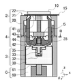
- FIG. 1A is a plan view showing an open state of an example of a form embodying the present invention, and shows a state immediately before picking up one semiconductor chip with four claws.
- 1B is a cross-sectional view showing an open state of an example of a form embodying the present invention, and shows a cross-section taken along line AA in FIG. 1A.
- the three axes of the orthogonal coordinate system are X, Y, and Z
- the XY plane is the horizontal plane
- the Z direction is the vertical direction.
- the direction of the arrow is represented as the top, and the opposite direction is represented as the bottom.
- the rotation direction centered on the X direction is defined as the ⁇ x direction
- the rotation direction centered on the Y direction is defined as the ⁇ y direction.
- the pickup device 1 includes a housing 2, an in-casing slider portion 3, a claw portion 4, an upper limit stopper portion 5, and an actuator 6.
- a housing 2 an in-casing slider portion 3, a claw portion 4, an upper limit stopper portion 5, and an actuator 6.
- the case where four claw portions 4 are arranged at an angle of 90 degrees when viewed in plan will be described as an example.
- the housing 2 is configured to include a substantially cylindrical hollow body body 20 and a support surface 21 structured to cover the upper end side of the housing body 20.
- the support surface 21 has a circular plane and has an opening 22 in a part of the surface.
- the opening 22 is connected to a vacuum source through piping and a switching valve. Since the housing
- the in-housing slider 3 is disposed inside the housing 2 and has a structure that can slide inside the housing 2.
- a support pin 35 is attached to the slider 3 in the housing, and the claw portion 4 is attached to the support pin 35.
- claw part 4 is substantially L-shaped, the nail
- the claw other end side upper side 43 is called the claw other end side lower side 44 and the claw other end side lower side is called the claw other end lower side 44.
- the claw body bent portion 42 is provided with a hole through which the support pin 35 is passed, and the claw tip portion 41 can be rotated in the ⁇ x direction or the ⁇ y direction with the support pin 35 as a rotation center.
- the claw portions 4 are arranged symmetrically as a pair. Furthermore, you may arrange
- An upper limit stopper portion 5 is attached inside the housing 2, and the slider 30 in the housing slides to raise the entire claw portion 4, and after or after the claw tip portion 41 projects from the opening 22 by a predetermined dimension. It is comprised so that the nail
- the claw tip 41 rotates to the contact point side as long as the contact point is on the right side of the support pin 35 as in the left claw 4 shown in FIG. 1B. If the contact point is on the left side with respect to the support pin 35 as in the right claw portion 4 shown in FIG. 1B, it means that the claw tip portion 41 is rotated counterclockwise. . That is, as shown in FIGS. 1A and 1B, when the four claw portions 4 are arranged every 90 degrees and the abutting point is inside the support pins 35, the claw tip portions 41a to 41d are raised. However, it can be rotated so as to approach each other while narrowing the interval.
- the claw tip portions 41a to 41d peel off the adhesive sheet 15 from the end portion of the semiconductor chip 10 to the inside while pushing up the semiconductor chip 10 as the in-casing slider portion 3 rises. be able to.
- the upper end 43 of the other end of the claw comes into contact with the upper limit stopper portion 5, whether the claw tip portions 41a to 41d are located above, below or at the same height as the opening 22 is described in detail later.
- the amount of movement in the direction and the vertical direction may be determined by appropriately designing the dimensions of each part of the claw part 4.
- the pickup device 1 is provided with an actuator 6, and the actuator 6 includes an actuator body 60 and a movable part 61.
- the actuator 6 has a structure capable of controlling ON / OFF operation from the outside, and the movable portion 61 is positioned below in the OFF state.
- the actuator main body 60 is attached to the housing main body 20 via a connecting member or the like. Alternatively, the actuator body 60 may be directly attached to the housing body 20.
- the in-casing slider 30 has a claw pressing portion 32 disposed at a position where it comes into contact with the lower side 44 of the other end of the claw, and the claw other end portion upper side 43 is not in contact with the upper limit stopper 5.
- the distal end portion 41 may be configured to rotate to the opposite side of the contact point between the lower end 44 of the other end of the claw and the claw pressing portion 32.
- the aforementioned claw tip 41 rotates to the side opposite to the contact point. If the aforementioned contact point is on the right side with respect to the support pin 35 as in the left claw 4 shown in FIG. Is rotated counterclockwise, and if the abutment point is on the left side with respect to the support pin 35 as in the right claw portion 4 shown in FIG. 1B, the claw tip portion 41 is rotated clockwise. means. In other words, as shown in FIGS. 1A and 1B, if the four claw portions 4 are arranged every 90 degrees and the abutting point is inward with respect to the support pins 35, the claw tip portions 41a to 41d are mutually connected. It rotates so that it may move away, and it stops in the state which the nail
- the claw pressing portion 32 is configured by an elastic body such as a rubber material, or is configured by attaching the claw pressing portion 32 to the concave portion at the center of the in-casing slider 30 via a spring 33 as shown in FIG. 1B. You may do it. Then, the lower side 44 of the other end of the claw is pushed up with an appropriate force, so that the claw tip end portions 41a to 41d are not unexpectedly closed when the in-casing slider 30 is raised. Further, in conjunction with the upward movement of the in-casing slider 30, the claw end portions 41a to 41d can be smoothly changed to the closed state while being lifted.
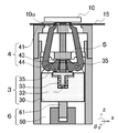
- FIG. 2A is a plan view showing a closed state of an example embodying the present invention, and shows a state immediately after one semiconductor chip is picked up by four claw portions.
- FIG. 2B is a cross-sectional view showing a closed state of an example of a form embodying the present invention, taken along line AA in FIG. 2A. An arrow cross section is shown.
- the actuator 6 is in the ON state and the movable portion 61 is moved upward as compared with the state shown in FIGS. 1A and 1B.
- Examples of the actuator 6 include a structure in which the movable portion 61 reciprocates in the vertical direction by air, hydraulic pressure, or electric power.
- the slider 3 and the support pin 35 are slid up and down by the ON / OFF operation of the actuator, and the nail body is raised by the support pin 35 rising.
- the bent part 42 is raised.
- claw part 4 raises as a whole, the nail
- raising 41 the structure which can be rotated in the ⁇ x direction or the ⁇ y direction is provided. As shown in FIG. 1B and FIG.
- the claw tip end portion 41 is closed inward by arranging the claw other end portion upper side 43 and the upper limit stopper portion 5 in contact with the inner side of the support pin 35.
- tip part 41 namely, claw front-end
- claw part 4 which makes a pair becomes an operation
- the semiconductor chip 10 When the semiconductor chip 10 is pushed up by the claw tip 41 as described above, a gap 10u is generated between the semiconductor chip 10 and the adhesive sheet 15 on the lower surface side. Thereafter, the semiconductor chip 10 is sucked by the suction nozzle of the transfer unit disposed above the semiconductor chip 10.
- the transfer unit is configured to lift the semiconductor chip sucked by the suction nozzle further upward to completely peel the semiconductor chip from the sheet and carry the peeled chip to the next process. At this time, the semiconductor chip 10 is smoothly taken out without being damaged because a wide range including the corners and edges on the lower surface side has already been peeled off from the adhesive sheet 15.
- FIG. 3 is a side view of a claw part used in an example of a form embodying the present invention. Focusing on one claw part 4, a claw tip part 41 and the other claw end with respect to the support pin 35 of the claw part 4 The position dimension with the part upper side 43 is shown.
- the horizontal dimension of the claw tip 41 is L1a
- the vertical dimension is L1z
- the horizontal dimension of the claw other end 43 upper side is L2a
- the vertical dimension is L2z.
- the upper side is represented as plus
- the lower side is represented as minus. If it arrange
- tip part is linear from beginning to end. On the other hand, if the nail tip portion is disposed outside the fulcrum and the distance between the nail tip portion and the support pin is set to be short, the movement locus of the nail tip portion becomes somewhat arcuate.
- tip part when it is set to + 2mm. At this time, as for a nail
- tip part when + 3mm and L2z + 2mm at this time.
- tip part ascending movement component from a close start to a close end is a straight line with the movement component of a close direction Is increasing.
- tip parts which comprise a pair are arrange
- the nail tip portion is arranged so as to first abut directly below or slightly inside the corner portion of the semiconductor chip to be picked up. Then, the four claw tip portions rotate while narrowing each other, thereby moving inward from the corner portion of the semiconductor chip having a square or rectangular outer shape. Therefore, the adhesive sheet is peeled off from each corner of the semiconductor chip, and the semiconductor chip can be smoothly removed from the adhesive sheet.
- tip part may be comprised only by a pair (namely, two pieces).
- the tip of the claw is arranged so as to correspond to the opposite side end in the longitudinal direction of the semiconductor chip to be picked up. Further, the tip of the claw is configured to be able to move inward while pushing up the tip while abutting with a length that is the same as or slightly shorter than the opposite side of the opposite end. If it demonstrates with reference to FIG. 1A, it is a case where the nail
- claw part is comprised only by a pair of 41a and 41b, and there is no claw front-end
- the movement ratio between the rise of the claw tip and the horizontal movement is set based on the trajectory of the arc movement. Therefore, when it is desired to change the change ratio, it is necessary to design and process the cross-sectional shape of the claw tip.
- the rise of the entire claw portion can be realized by lifting the support pin that penetrates the bent portion, which is the middle portion of the claw portion, via the slider in the housing.
- the movement of the claw tip portion in the horizontal direction is realized by further raising the support pin after the upper side of the other end of the claw comes into contact with the upper limit stopper that restricts the rise of the upper side of the other end of the claw.
- the conventional technology when trying to make the movement of the claw tip part a linear trajectory, it is necessary to lengthen the casing part in the thickness direction of the substrate and increase the distance between the claw tip part and the support pin. It is not realistic and tends to be low in rigidity.
- the method of the present invention if the position dimensions of the nail tip, the upper side of the other end of the nail and the support pin are appropriately determined, the distance between the nail tip and the support pin can be reduced without extremely increasing the distance between the nail tip and the support pin. The rising component can be reduced. Therefore, the vertical dimension of the housing can be made compact, and the rigidity can be easily maintained.
Landscapes
- Container, Conveyance, Adherence, Positioning, Of Wafer (AREA)
- Die Bonding (AREA)
Abstract
粘着シートに貼られた半導体チップにダメージを与えず、確実に粘着シートから取り外すことができ、多品種に対応できるピックアップ装置を提供する。 具体的には、粘着シートに貼られた半導体チップのピックアップ装置において、 半導体チップを支持する筐体と、ピックアップされる半導体チップを押し上げる爪部とを備え、 筐体にはサポート面と開口部が備えられ、 爪部は、 半導体チップを押し上げる爪先端部と、爪本体屈曲部と、爪上側他端部とを有し、 爪本体屈曲部には、支持ピンを通す孔部が備えられており、 筐体内部には、筐体内スライダ部と、上限ストッパ部とが備えられ、 筐体内スライダ部をスライドさせることにより、支持ピンが上昇して爪先端部が上昇するとともに、爪上側他端部が上限ストッパ部と当接することで爪先端部が半導体チップ内側へ向かって閉じる機構を備えていることを特徴とする、 半導体チップのピックアップ装置。
Description
本発明は、粘着シートに貼られた半導体チップを前記粘着シートから取り外す半導体チップのピックアップ装置に関する。
粘着シートに貼りつけて縦横方向に格子状に切断された半導体ウエハから、半導体チップを1つずつ取り外すために、その半導体チップと粘着シートとの粘着力を弱め、ピックアップするということが、従来から行われてきた。このピックアップには種々の方式があり、予め半導体チップを吸引ノズルで吸引保持した状態から粘着シートを剥離させるもの(例えば特許文献1,2)や、半導体チップを粘着シートから剥離させながらピックアップして吸引ノズルで保持するもの(例えば特許文献3)が従来からある。
半導体チップは薄板化が進んでおり、欠けや割れが起きやすい薄板化された半導体チップに、過度のストレスを加えることなくピックアップすることが求められている。
そのため、薄板化された半導体チップにダメージを与えない様にピックアップ機構を、薄いチップ用に最適設定化するなどして対応させていた。
そのため、薄板化された半導体チップにダメージを与えない様にピックアップ機構を、薄いチップ用に最適設定化するなどして対応させていた。
しかし、実際の生産工程においては品種替えなどがあり、薄板化された半導体チップだけでなく、従来からある厚みのある半導体チップも、同じ装置を使ってピックアップする場面が多くある。また、1つのシートには多数個に分割された半導体チップが貼り付いており、その状態から半導体チップを1つずつ取り外すため、ピックアップ対象となるチップの周囲に他の半導体チップが多数貼り付いている場合と、概ね半導体チップの取り外しが進み、ピックアップ対象となる半導体チップの周囲に他の半導体チップがない場合と、これらの中間の状態で部分的に他の半導体チップが隣接して存在する場合など、ピックアップ対象となる半導体チップが貼り付いているシートにかかる内部応力には、大きな差が生じている。そのため、多様な品種に対応できるピックアップ装置が求められてきた。
そこで本発明は、粘着シートに貼られた半導体チップにダメージを与えず、確実に粘着シートから取り外すことができ、多様な品種に対応できるピックアップ装置を提供することを目的としている。
以上の課題を解決するために、請求項1に記載の発明は、
粘着シートに貼られた半導体チップを前記粘着シートから取り外す半導体チップのピックアップ装置において、
ピックアップされる半導体チップを粘着シート側から支持する筐体と、
前記ピックアップされる半導体チップを粘着シート側から押し上げる複数の爪部とを備え、
前記筐体には、
前記半導体チップ下面側を支持するサポート面と、
前記サポート面に設けられた開口部とが備えられ、
前記爪部は、
前記開口部から突出して半導体チップを押し上げる爪先端部と、爪本体屈曲部と、爪他端部上側とを有し、
前記爪本体屈曲部には、前記爪先端部の回動動作の中心軸となる孔部が備えられており、
前記筐体内部には、
前記筐体内部をスライドできる筐体内スライダ部と、
前記爪他端部上側の上昇を制限する上限ストッパ部とが備えられ、
前記筐体内スライダ部には、
前記爪本体屈曲部の孔部を通る支持ピンが取り付けられており、
前記筐体内スライダ部をスライドさせることにより前記支持ピンが上昇し、前記爪先端部が上昇して前記開口部から突出しつつ、前記爪他端部上側が前記上限ストッパ部と当接することで前記爪先端部が、前記爪他端部上側と前記上限ストッパ部との当接点側に回動する構造を有していることを特徴とする、
半導体チップのピックアップ装置である。
粘着シートに貼られた半導体チップを前記粘着シートから取り外す半導体チップのピックアップ装置において、
ピックアップされる半導体チップを粘着シート側から支持する筐体と、
前記ピックアップされる半導体チップを粘着シート側から押し上げる複数の爪部とを備え、
前記筐体には、
前記半導体チップ下面側を支持するサポート面と、
前記サポート面に設けられた開口部とが備えられ、
前記爪部は、
前記開口部から突出して半導体チップを押し上げる爪先端部と、爪本体屈曲部と、爪他端部上側とを有し、
前記爪本体屈曲部には、前記爪先端部の回動動作の中心軸となる孔部が備えられており、
前記筐体内部には、
前記筐体内部をスライドできる筐体内スライダ部と、
前記爪他端部上側の上昇を制限する上限ストッパ部とが備えられ、
前記筐体内スライダ部には、
前記爪本体屈曲部の孔部を通る支持ピンが取り付けられており、
前記筐体内スライダ部をスライドさせることにより前記支持ピンが上昇し、前記爪先端部が上昇して前記開口部から突出しつつ、前記爪他端部上側が前記上限ストッパ部と当接することで前記爪先端部が、前記爪他端部上側と前記上限ストッパ部との当接点側に回動する構造を有していることを特徴とする、
半導体チップのピックアップ装置である。
上記半導体チップのピックアップ装置を用いるので、
粘着シートを吸着保持する力が強かったり、粘着シートの伸縮率が低かったりして、粘着シートからの反力が大きくても、半導体チップを持ち上げる動作が妨げられず、ピックアップしたい半導体チップを確実に持ち上げることができる。
粘着シートを吸着保持する力が強かったり、粘着シートの伸縮率が低かったりして、粘着シートからの反力が大きくても、半導体チップを持ち上げる動作が妨げられず、ピックアップしたい半導体チップを確実に持ち上げることができる。
請求項2に記載の発明は、
前記爪部はさらに爪下側他端部を有し、
前記筐体内スライダ部には、さらに前記爪下側他端部を当接しながら押し上げる、爪押さえ部が取り付けられていることを特徴とする、
請求項1に記載の半導体チップのピックアップ装置である。
前記爪部はさらに爪下側他端部を有し、
前記筐体内スライダ部には、さらに前記爪下側他端部を当接しながら押し上げる、爪押さえ部が取り付けられていることを特徴とする、
請求項1に記載の半導体チップのピックアップ装置である。
上記半導体チップのピックアップ装置を用いれば、
前記爪他端部下側に上向きの力を加えておくことができるため、前記爪先端部が不意に回動することを防ぐことができる。さらに、前記筐体内スライダ部が下方に位置するときは、前記爪先端部を常に開放状態にしておくことができ、前記筐体内スライダ部の上昇とともに徐々に爪先端部が閉じる動作をスムーズに行うことができる。
前記爪他端部下側に上向きの力を加えておくことができるため、前記爪先端部が不意に回動することを防ぐことができる。さらに、前記筐体内スライダ部が下方に位置するときは、前記爪先端部を常に開放状態にしておくことができ、前記筐体内スライダ部の上昇とともに徐々に爪先端部が閉じる動作をスムーズに行うことができる。
請求項3に記載の発明は、
前記爪部が4本備えられており、
前記爪部が2本一対で、当該一対を構成する前記爪部先端部が互いに対向して配置されており、前記筐体内スライダ部をスライドさせることにより、前記爪先端部が互いの間隔を狭めながら回動する構造を有している
ことを特徴とする、請求項1又は請求項2に記載の半導体チップのピックアップ装置である。
前記爪部が4本備えられており、
前記爪部が2本一対で、当該一対を構成する前記爪部先端部が互いに対向して配置されており、前記筐体内スライダ部をスライドさせることにより、前記爪先端部が互いの間隔を狭めながら回動する構造を有している
ことを特徴とする、請求項1又は請求項2に記載の半導体チップのピックアップ装置である。
上記半導体チップのピックアップ装置を用いれば、
四角形の半導体チップの角部から内側に向けて、確実に粘着シートを剥離できるので、薄い半導体チップのピックアップには好適である。
四角形の半導体チップの角部から内側に向けて、確実に粘着シートを剥離できるので、薄い半導体チップのピックアップには好適である。
粘着シートに貼られた半導体チップにダメージを与えず、確実に粘着シートから取り外すことができ、多様な品種に対応できる。
本発明を実施するための形態について、図を用いながら説明する。
図1Aは、本発明を具現化する形態の一例の開状態を示す平面図であり、1つの半導体チップを4本の爪部でピックアップさせる直前の状態を示している。
図1Bは、本発明を具現化する形態の一例の開状態を示す断面図であり、図1AのA-A矢視断面を示している。
各図において直交座標系の3軸をX、Y、Zとし、XY平面を水平面、Z方向を鉛直方向
とする。特にZ方向は矢印の方向を上とし、その逆方向を下と表現する。また、X方向を軸中心とする回転方向をθx方向とし、Y方向を軸中心とする回転方向をθy方向とする。
図1Aは、本発明を具現化する形態の一例の開状態を示す平面図であり、1つの半導体チップを4本の爪部でピックアップさせる直前の状態を示している。
図1Bは、本発明を具現化する形態の一例の開状態を示す断面図であり、図1AのA-A矢視断面を示している。
各図において直交座標系の3軸をX、Y、Zとし、XY平面を水平面、Z方向を鉛直方向
とする。特にZ方向は矢印の方向を上とし、その逆方向を下と表現する。また、X方向を軸中心とする回転方向をθx方向とし、Y方向を軸中心とする回転方向をθy方向とする。
ピックアップ装置1は、筐体2と、筐体内スライダ部3と、爪部4と、上限ストッパ部5と、アクチュエータ6とを含んで構成されている。ここでは、爪部4が4本、それぞれ平面視した場合に90度の角度をなして配置されている場合を例示して説明する。
筐体2は、略円筒形の中空形状をした筐体本体部20と、筐体本体部20の上端側を蓋するような構造のサポート面21とを含んで構成されている。前記サポート面21は、円形平面をしており、表面の一部には開口部22を有している。開口部22は、配管及び切替バルブなどを通じて真空源に接続されている。筐体2は、このような構造を備えているので、粘着シートに貼られた半導体チップをサポート面21で支持しつつ、開口部22の範囲で粘着シートを部分的に吸着保持できる。
筐体内スライダ3は、筐体2の内部に配置されて、筐体2の内部をスライドできるような構造を備えている。筐体内スライダ3には、支持ピン35が取り付けられており、支持ピン35には、爪部4が取り付けられている。
爪部4は、略L字型をしており、半導体チップが貼り付けられた粘着シート側を爪先端部41、屈曲している部分を爪本体屈曲部42、爪先端部41でない他端側の上側を爪他端部上側43、爪先端部41でない他端側の下側を爪他端部下側44と称する。爪本体屈曲部42には、支持ピン35を通す孔が設けられており、爪先端部41は、支持ピン35を回転中心として、θx方向又はθy方向に回動できるようになっている。
爪部4は、例えば図1A,図1Bに示すように、2本を1対として対称的に配置する。さらに、4本の爪部4を、2対が互いに交差するように配置しても良い。
爪部4は、例えば図1A,図1Bに示すように、2本を1対として対称的に配置する。さらに、4本の爪部4を、2対が互いに交差するように配置しても良い。
筐体2内部には、上限ストッパ部5が取り付けられており、筐体内スライダ30がスライドして爪部4全体が上昇し、爪先端部41が開口部22から所定寸法だけ突出した後又は突出する前に、爪他端部上側43が上限ストッパ部5に当接するように、構成されている。そして、筐体内スライダ30とともに支持ピン35が上昇を続けても、上限ストッパ部5が爪他端部上側43の上昇を制限するため、爪先端部41は、上昇しながら、爪他端部上側43と上限ストッパ5との当接点側に回動する。
前述の爪先端部41が当接点側に回動するとは、図1Bに示す左側の爪部4の様に支持ピン35に対して前述の当接点が右側にあれば、爪先端部41が時計回りに回動し、図1Bに示す右側の爪部4の様に支持ピン35に対して前述の当接点が左側にあれば、爪先端部41が反時計回りに回動することを意味する。
つまり、図1A,図1Bように90度毎に4本の爪部4を配置し、それらの支持ピン35に対して前述の当接点が内側にあれば、爪先端部41a~41dは、上昇しつつ、互いに間隔を狭めながら近づき合うように回動することができる。
つまり、図1A,図1Bように90度毎に4本の爪部4を配置し、それらの支持ピン35に対して前述の当接点が内側にあれば、爪先端部41a~41dは、上昇しつつ、互いに間隔を狭めながら近づき合うように回動することができる。
そうすることで、爪先端部41a~41dは、筐体内スライダ部3が上昇することで、半導体チップ10を上方に押し上げつつ、半導体チップ10の端部から内側に向けて粘着シート15を剥離することができる。
尚、爪他端部上側43が上限ストッパ部5に当接したときに、爪先端部41a~41dが開口部22より上側、下側若しくは同じ高さのいずれにするか、詳細を後述する水平方向及び垂直方向の移動量などは、爪部4の各部の寸法を適宜設計して決定すれば良い。
尚、爪他端部上側43が上限ストッパ部5に当接したときに、爪先端部41a~41dが開口部22より上側、下側若しくは同じ高さのいずれにするか、詳細を後述する水平方向及び垂直方向の移動量などは、爪部4の各部の寸法を適宜設計して決定すれば良い。
ピックアップ装置1には、アクチュエータ6が取り付けられており、アクチュエータ6は、アクチュエータ本体部60と可動部61とを含んで構成されている。アクチュエータ6は、外部からのON/OFF動作制御が可能な構造をしており、OFF状態の時は可動部61が下方に位置している。アクチュエータ本体部60は、筐体本体部20に連結部材などを介して取り付けられている。あるいは、アクチュエータ本体部60を筐体本体部20に直接取り付けても良い。
さらに、筐体内スライダ30は、爪他端部下側44と当接する位置に、爪押さえ部32を配置し、爪他端部上側43が上限ストッパ5と当接していない状態にあっては、爪先端部41が、爪他端部下側44と爪押さえ部32との当接点と反対側に回動する構造にしても良い。
前述の爪先端部41が当接点と反対側に回動するとは、図1Bに示す左側の爪部4の様に支持ピン35に対して前述の当接点が右側にあれば、爪先端部41が反時計回りに回動し、図1Bに示す右側の爪部4の様に支持ピン35に対して前述の当接点が左側にあれば、爪先端部41が時計回りに回動することを意味する。
つまり、図1A,図1Bように90度毎に4本の爪部4を配置し、それらの支持ピン35に対して前述の当接点が内側にあれば、爪先端部41a~41dは、互いに遠ざかるように回動し、爪部4と筐体2とが接触した状態で静止し、開放状態となる。
つまり、図1A,図1Bように90度毎に4本の爪部4を配置し、それらの支持ピン35に対して前述の当接点が内側にあれば、爪先端部41a~41dは、互いに遠ざかるように回動し、爪部4と筐体2とが接触した状態で静止し、開放状態となる。
爪押さえ部32は、ゴム材料などの弾性体により構成したり、図1Bに示すように、筐体内スライダ30の中央部の凹み部にスプリング33を介して爪押さえ部32を取り付けて構成したりしても良い。そうすれば、爪他端部下側44が適当な力で押し上げられるため、筐体内スライダ30が上昇する際に、爪部先端部41a~41dが不意に閉じることが無くなる。さらに、筐体内スライダ30の上昇動作に連動して、爪部先端部41a~41dが上昇しながらスムーズに互いに閉状態に変化させることができる。
図2Aは、本発明を具現化する形態の一例の閉状態を示す平面図であり、1つの半導体チップを4本の爪部でピックアップさせた直後の状態を示している。
図2Bは、本発明を具現化する形態の一例の閉状態を示す断面図であり、図2AのA-A
矢視断面を示している。
図2A及び図2Bで示す図の状態では、図1A及び図1Bで示した状態と比較すると、アクチュエータ6がON状態となり、可動部61が上方に移動している。アクチュエータ6としては、エア、油圧又は電動で可動部61が上下方向に往復移動する構造のものが例示できる。
図2Bは、本発明を具現化する形態の一例の閉状態を示す断面図であり、図2AのA-A
矢視断面を示している。
図2A及び図2Bで示す図の状態では、図1A及び図1Bで示した状態と比較すると、アクチュエータ6がON状態となり、可動部61が上方に移動している。アクチュエータ6としては、エア、油圧又は電動で可動部61が上下方向に往復移動する構造のものが例示できる。
本発明のピックアップ装置1は、上述のような構造を備えているので、前記アクチュエータのON/OFF動作により、筐体内スライダ3及び支持ピン35を上下にスライドさせ、支持ピン35の上昇により爪本体屈曲部42を上昇させる。そして、爪部4が全体的に上昇する一方で、筐体本体部2の内部に固定されている上限ストッパ部5の作用により爪他端部上側43の上昇を制限することで、爪先端部41を上昇させつつ、θx方向又はθy方向に回動させることができる構造を備えている。図1B及び図2Bに示すように、支持ピン35よりも内側に、爪他端部上側43と上限ストッパ部5とが当接するように配置することで、爪先端部41が内側に閉じる動作を具現化できる。そして、対をなしている爪部4の爪先端部41(つまり、爪先端部41aと41b、41cと41d)は、互いに間隔が狭まりながらチップを押し上げる動作となる。
半導体チップ10は、上述のようにして爪先端部41により押し上げられると、下面側の粘着シート15との間に隙間10uが生じる。その後、半導体チップ10は、その上方に配置された移載部の吸引ノズルにより吸引される。そして、前記移載部は、吸引ノズルにより吸引した前記半導体チップを、さらに上方に持ち上げて完全にシートから剥離し、前記剥離したチップを次工程に運ぶように構成されている。このとき、半導体チップ10は、下面側の角部や端部を含めた広い範囲が既に粘着シート15から剥離しているので、ダメージを与えられることなくスムーズに取り出される。
[爪形状による剥離動作の違い]
本発明を適用させ、爪部4の各寸法を適宜設定することで、爪先端部41の上昇中の軌跡は、任意に変化させることができる。
図3は、本発明を具現化する形態の一例に用いられる爪部の側面図であり、1つの爪部4について着目し、爪部4の支持ピン35に対する、爪先端部41と爪他端部上側43との位置寸法を示している。
本発明を適用させ、爪部4の各寸法を適宜設定することで、爪先端部41の上昇中の軌跡は、任意に変化させることができる。
図3は、本発明を具現化する形態の一例に用いられる爪部の側面図であり、1つの爪部4について着目し、爪部4の支持ピン35に対する、爪先端部41と爪他端部上側43との位置寸法を示している。
支持ピン35の中心を基準点とし、爪先端部41の水平方向の寸法をL1a、垂直方向の寸法をL1z、爪他端部上側43の水平方向の寸法をL2a、垂直方向の寸法をL2zと定義する。水平方向は、爪が閉じる方向をプラスとし、爪が開く方向をマイナスとして表す。垂直方向は、上側をプラスとし、下側をマイナスとして表す。
爪先端部が、支点よりも内側になるように配置すれば、爪先端部は少しずつ上昇しながら、内側に閉じ、終始、爪先端部の移動軌跡は直線的である。
一方、爪先端部が、支点よりも外側になるように配置し、爪先端部と支持ピンとの間隔を短めに設定すれば、爪先端部の移動軌跡はやや円弧状に近くなる。
爪先端部が、支点よりも内側になるように配置すれば、爪先端部は少しずつ上昇しながら、内側に閉じ、終始、爪先端部の移動軌跡は直線的である。
一方、爪先端部が、支点よりも外側になるように配置し、爪先端部と支持ピンとの間隔を短めに設定すれば、爪先端部の移動軌跡はやや円弧状に近くなる。
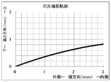
図4は、本発明を具現化する形態の一例に用いられる爪先端部の軌跡を示す図であり、図3に示した各寸法をそれぞれ、L1a=+1mm、L1z=+10mm、L2a=+3mm、L2z=+2mmとしたときの、爪先端部の上昇中の軌跡を示す図である
このとき爪先端部は、閉じ始めから閉じ終わりまでの上昇移動成分が、閉じる方向の移動成分と比較して小さくなっている。
このとき爪先端部は、閉じ始めから閉じ終わりまでの上昇移動成分が、閉じる方向の移動成分と比較して小さくなっている。
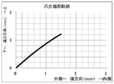
図5は、本発明を具現化する形態の別の例に用いられる爪先端部の軌跡を示す図であり、図3に示した各寸法をそれぞれ、L1a=-1mm、L1z=+10mm、L2a=+3mm、L2z=+2mmとしたときの、爪先端部の上昇中の軌跡を示す図である
このとき爪先端部は、閉じ始めから閉じ終わりまでの上昇移動成分が、閉じる方向の移動成分と概ね直線的に増加している。
このとき爪先端部は、閉じ始めから閉じ終わりまでの上昇移動成分が、閉じる方向の移動成分と概ね直線的に増加している。
図6は、本発明を具現化する形態のさらに別の例に用いられる爪先端部の軌跡を示す図であり、図3に示した各寸法をそれぞれ、L1a=-1.5mm、L1z=+5mm、L2a=+3.5mm、L2z=+0mmとしたときの、爪先端部の上昇中の軌跡を示す図である。このとき爪先端部は、閉じ始めから閉じ終わりまでの上昇移動成分が、閉じる方向の移動成分と概ね比例的に増加している。
上述では、爪部及び爪先端部が二対(つまり4本)ある場合について説明をした。この場合、対をなしている爪先端部同士がが対向して配置されていることが好ましい。さらには、爪先端部がピックアップ対象となる半導体チップの角部の直下あるいは角部よりやや内側にまず当接するように配置することが、より好ましい。そうすれば、4本ある爪先端部が互いの間隔を狭めながら回動することで、正方形や長方形の外形をした半導体チップの角部から内側へ移動する。そのため、半導体チップの各角部から粘着シートが剥がれ、粘着シートから半導体チップをスムーズに取り外すことができる。
一方、爪部及び爪先端部は、一対(つまり2本)のみで構成されていても良い。この場合、爪先端部をピックアップ対象となる半導体チップの長手方向の対辺端部に対応するように配置する。さらに、爪先端部は、前記対辺端部の対辺と同じか少し短い長さで当接しながら当該チップを押し上げつつ、内側へ向かって移動できるように構成する。図1Aを参考にして説明するならば、爪部を構成する爪先端部が41aと41bの一対のみで構成され、図1Aで図示された爪先端部41cと41dが無い構成の場合である。
そうすれば、細長い形状の半導体チップであっても、本発明を適用させて、粘着シートからスムーズに取り外すことができる。
そうすれば、細長い形状の半導体チップであっても、本発明を適用させて、粘着シートからスムーズに取り外すことができる。
[従来技術との相違点]
従来の技術(例えば、特許文献3)では、爪先端部の上昇と水平動作との動作比率は、円弧動作の軌跡に基づいて設定されていた。そのため、その変化比率を変化させたい場合、爪先端部の断面形状を設計し加工する必要があった。しかし、本発明の方式であれば、爪部全体の上昇は、爪部の中途部である屈曲部を貫通する支持ピンを、筐体内スライダを介して持ち上げることで具現化できる。爪先端部の水平方向の移動は、爪他端部上側が、爪他端部上側の上昇を制限する上限ストッパと当接した後、さらに支持ピンが上昇することで具現化されている。
従来の技術(例えば、特許文献3)では、爪先端部の上昇と水平動作との動作比率は、円弧動作の軌跡に基づいて設定されていた。そのため、その変化比率を変化させたい場合、爪先端部の断面形状を設計し加工する必要があった。しかし、本発明の方式であれば、爪部全体の上昇は、爪部の中途部である屈曲部を貫通する支持ピンを、筐体内スライダを介して持ち上げることで具現化できる。爪先端部の水平方向の移動は、爪他端部上側が、爪他端部上側の上昇を制限する上限ストッパと当接した後、さらに支持ピンが上昇することで具現化されている。
また、従来の技術では、爪先端部の動きを直線的な軌跡にしようとする場合は、筐体部を基板の厚み方向に長くし、爪先端部と支持ピンとの距離を長くする必要があり、現実的ではなく、剛性も低くなりがちである。しかし、本発明の方式であれば、爪先端部、爪他端部上側及び支持ピンの位置寸法を適宜決定すれば、爪先端部と支持ピンとの距離を極端に大きくすることなく爪先端部の上昇成分を小さくすることができる。そのため、筐体の上下方向の寸法をコンパクトにすることができ、剛性を保つことも容易となる。
[別の利点]
従来の技術では、薄板化された半導体チップのピックアップに好適な構成として、剥離手段である爪部のスムーズな開閉動作のために、ばね付勢力を弱くすると、粘着シートを吸着保持する力が強かったり、粘着シートの伸縮が少ない場合には、半導体チップがバックアップ体から持ち上げられる前に、爪部の先端部が閉じてしまう(いわゆる、空振り)現象が起きる場合があった。一方、空振り現象を避けるために、ばね付勢力を強くしてしまうと、爪部のスムーズな開閉動作が妨げられたり、振動や衝撃が発生したりして、薄板化された半導体チップに割れや欠けを生じさせずに粘着シートから取り外すことが難しくなる場合がある。しかし、本発明の構成によれば、開閉機構の構造および開閉動作の原理が異なっているため、爪部の開閉動作をスムーズ、かつ、確実に行うことが容易となり、多様な品種にも対応できる。
従来の技術では、薄板化された半導体チップのピックアップに好適な構成として、剥離手段である爪部のスムーズな開閉動作のために、ばね付勢力を弱くすると、粘着シートを吸着保持する力が強かったり、粘着シートの伸縮が少ない場合には、半導体チップがバックアップ体から持ち上げられる前に、爪部の先端部が閉じてしまう(いわゆる、空振り)現象が起きる場合があった。一方、空振り現象を避けるために、ばね付勢力を強くしてしまうと、爪部のスムーズな開閉動作が妨げられたり、振動や衝撃が発生したりして、薄板化された半導体チップに割れや欠けを生じさせずに粘着シートから取り外すことが難しくなる場合がある。しかし、本発明の構成によれば、開閉機構の構造および開閉動作の原理が異なっているため、爪部の開閉動作をスムーズ、かつ、確実に行うことが容易となり、多様な品種にも対応できる。
1 ピックアップ装置
2 筐体
3 筐体内スライダ部
4 爪部
5 上限ストッパ部
6 アクチュエータ
10 半導体チップ
12 角部
15 粘着シート
20 筐体本体部
21 サポート面
22 開口部
30 スライダ本体部
32 爪押さえ部
33 スプリング
35 支持ピン
41 爪先端部
42 爪本体屈曲部
43 爪他端部上側
44 爪他端部下側
60 アクチュエータ本体部
61 可動部
2 筐体
3 筐体内スライダ部
4 爪部
5 上限ストッパ部
6 アクチュエータ
10 半導体チップ
12 角部
15 粘着シート
20 筐体本体部
21 サポート面
22 開口部
30 スライダ本体部
32 爪押さえ部
33 スプリング
35 支持ピン
41 爪先端部
42 爪本体屈曲部
43 爪他端部上側
44 爪他端部下側
60 アクチュエータ本体部
61 可動部
Claims (3)
- 粘着シートに貼られた半導体チップを前記粘着シートから取り外す半導体チップのピックアップ装置において、
ピックアップされる半導体チップを粘着シート側から支持する筐体と、
前記ピックアップされる半導体チップを粘着シート側から押し上げる複数の爪部とを備え、
前記筐体には、
前記半導体チップ下面側を支持するサポート面と、
前記サポート面に設けられた開口部とが備えられ、
前記爪部は、
前記開口部から突出して半導体チップを押し上げる爪先端部と、爪本体屈曲部と、爪他端部上側とを有し、
前記爪本体屈曲部には、前記爪先端部の回動動作の中心軸となる孔部が備えられており、
前記筐体内部には、
前記筐体内部をスライドできる筐体内スライダ部と、
前記爪他端部上側の上昇を制限する上限ストッパ部とが備えられ、
前記筐体内スライダ部には、
前記爪本体屈曲部の孔部を通る支持ピンが取り付けられており、
前記筐体内スライダ部をスライドさせることにより前記支持ピンが上昇し、前記爪先端部が上昇して前記開口部から突出しつつ、前記爪他端部上側が前記上限ストッパ部と当接することで前記爪先端部が、前記爪他端部上側と前記上限ストッパ部との当接点側に回動する構造を有していることを特徴とする、
半導体チップのピックアップ装置。
- 前記爪部はさらに爪下側他端部を有し、
前記筐体内スライダ部には、さらに前記爪下側他端部を当接しながら押し上げる、爪押さえ部が取り付けられていることを特徴とする、
請求項1に記載の半導体チップのピックアップ装置。
- 前記爪部が4本備えられており、
前記爪部が2本一対で、当該一対を構成する前記爪部先端部が互いに対向して配置されており、前記筐体内スライダ部をスライドさせることにより、前記爪先端部が互いの間隔を狭めながら回動する構造を有している
ことを特徴とする、請求項1又は請求項2に記載の半導体チップのピックアップ装置。
Applications Claiming Priority (2)
| Application Number | Priority Date | Filing Date | Title |
|---|---|---|---|
| JP2011100735A JP2012234882A (ja) | 2011-04-28 | 2011-04-28 | 半導体チップのピックアップ装置 |
| JP2011-100735 | 2011-04-28 |
Publications (1)
| Publication Number | Publication Date |
|---|---|
| WO2012147725A1 true WO2012147725A1 (ja) | 2012-11-01 |
Family
ID=47072243
Family Applications (1)
| Application Number | Title | Priority Date | Filing Date |
|---|---|---|---|
| PCT/JP2012/060937 Ceased WO2012147725A1 (ja) | 2011-04-28 | 2012-04-24 | 半導体チップのピックアップ装置 |
Country Status (3)
| Country | Link |
|---|---|
| JP (1) | JP2012234882A (ja) |
| TW (1) | TW201304051A (ja) |
| WO (1) | WO2012147725A1 (ja) |
Cited By (6)
| Publication number | Priority date | Publication date | Assignee | Title |
|---|---|---|---|---|
| WO2014134387A1 (en) * | 2013-02-28 | 2014-09-04 | Texas Instruments Incorporated | Pick-up tip assembly |
| JP2016226285A (ja) * | 2016-06-30 | 2016-12-28 | 三菱電機株式会社 | モータ駆動回路、およびそれを内蔵した駆動回路内蔵モータならびに駆動回路内蔵ポンプモータ、およびそれらを搭載した空気調和機、換気扇、ヒートポンプ給湯機、ならびに内蔵冷温水循環式空調機 |
| CN111302032A (zh) * | 2020-03-12 | 2020-06-19 | 许伟波 | 一种能对箱子进行旋转的桁架分箱机械人 |
| JP2021072323A (ja) * | 2019-10-29 | 2021-05-06 | キヤノントッキ株式会社 | 基板剥離装置、基板処理装置、及び基板剥離方法 |
| JP2021072322A (ja) * | 2019-10-29 | 2021-05-06 | キヤノントッキ株式会社 | 基板保持部材、基板保持装置、基板処理装置、基板保持方法、成膜方法、及び電子デバイスの製造方法 |
| JP2021072321A (ja) * | 2019-10-29 | 2021-05-06 | キヤノントッキ株式会社 | 基板保持装置、基板処理装置、基板保持方法、成膜方法、及び電子デバイスの製造方法 |
Families Citing this family (5)
| Publication number | Priority date | Publication date | Assignee | Title |
|---|---|---|---|---|
| WO2014185446A1 (ja) | 2013-05-14 | 2014-11-20 | 東レエンジニアリング株式会社 | 半導体チップのピックアップ装置 |
| JP6941513B2 (ja) * | 2017-09-07 | 2021-09-29 | ファスフォードテクノロジ株式会社 | 半導体製造装置および半導体装置の製造方法 |
| JP2019140232A (ja) * | 2018-02-09 | 2019-08-22 | トヨタ自動車株式会社 | 剥離装置 |
| CN110641998B (zh) * | 2019-10-14 | 2021-05-04 | 珠海格力智能装备有限公司 | 夹具及具有其的输送设备 |
| JP2024023001A (ja) * | 2022-08-08 | 2024-02-21 | 日本電気株式会社 | ピックアップ装置およびピックアップ装置の制御方法 |
Citations (2)
| Publication number | Priority date | Publication date | Assignee | Title |
|---|---|---|---|---|
| JPH08255804A (ja) * | 1995-03-17 | 1996-10-01 | Iwate Toshiba Electron Kk | 半導体製造装置 |
| JP2005197368A (ja) * | 2004-01-05 | 2005-07-21 | Shibaura Mechatronics Corp | 半導体チップのピックアップ装置及びピックアップ方法 |
-
2011
- 2011-04-28 JP JP2011100735A patent/JP2012234882A/ja not_active Withdrawn
-
2012
- 2012-04-24 TW TW101114594A patent/TW201304051A/zh unknown
- 2012-04-24 WO PCT/JP2012/060937 patent/WO2012147725A1/ja not_active Ceased
Patent Citations (2)
| Publication number | Priority date | Publication date | Assignee | Title |
|---|---|---|---|---|
| JPH08255804A (ja) * | 1995-03-17 | 1996-10-01 | Iwate Toshiba Electron Kk | 半導体製造装置 |
| JP2005197368A (ja) * | 2004-01-05 | 2005-07-21 | Shibaura Mechatronics Corp | 半導体チップのピックアップ装置及びピックアップ方法 |
Cited By (9)
| Publication number | Priority date | Publication date | Assignee | Title |
|---|---|---|---|---|
| WO2014134387A1 (en) * | 2013-02-28 | 2014-09-04 | Texas Instruments Incorporated | Pick-up tip assembly |
| JP2016226285A (ja) * | 2016-06-30 | 2016-12-28 | 三菱電機株式会社 | モータ駆動回路、およびそれを内蔵した駆動回路内蔵モータならびに駆動回路内蔵ポンプモータ、およびそれらを搭載した空気調和機、換気扇、ヒートポンプ給湯機、ならびに内蔵冷温水循環式空調機 |
| JP2021072323A (ja) * | 2019-10-29 | 2021-05-06 | キヤノントッキ株式会社 | 基板剥離装置、基板処理装置、及び基板剥離方法 |
| JP2021072322A (ja) * | 2019-10-29 | 2021-05-06 | キヤノントッキ株式会社 | 基板保持部材、基板保持装置、基板処理装置、基板保持方法、成膜方法、及び電子デバイスの製造方法 |
| JP2021072321A (ja) * | 2019-10-29 | 2021-05-06 | キヤノントッキ株式会社 | 基板保持装置、基板処理装置、基板保持方法、成膜方法、及び電子デバイスの製造方法 |
| JP7057337B2 (ja) | 2019-10-29 | 2022-04-19 | キヤノントッキ株式会社 | 基板剥離装置、基板処理装置、及び基板剥離方法 |
| JP7057335B2 (ja) | 2019-10-29 | 2022-04-19 | キヤノントッキ株式会社 | 基板保持装置、基板処理装置、基板保持方法、成膜方法、及び電子デバイスの製造方法 |
| JP7057336B2 (ja) | 2019-10-29 | 2022-04-19 | キヤノントッキ株式会社 | 基板保持部材、基板保持装置、基板処理装置、基板保持方法、成膜方法、及び電子デバイスの製造方法 |
| CN111302032A (zh) * | 2020-03-12 | 2020-06-19 | 许伟波 | 一种能对箱子进行旋转的桁架分箱机械人 |
Also Published As
| Publication number | Publication date |
|---|---|
| JP2012234882A (ja) | 2012-11-29 |
| TW201304051A (zh) | 2013-01-16 |
Similar Documents
| Publication | Publication Date | Title |
|---|---|---|
| WO2012147725A1 (ja) | 半導体チップのピックアップ装置 | |
| JP4927979B2 (ja) | 半導体ダイのピックアップ装置及びその装置を用いた半導体ダイのピックアップ方法 | |
| JP5284144B2 (ja) | 半導体チップのピックアップ装置及びピックアップ方法 | |
| US20070293022A1 (en) | Method of and apparatus for detaching semiconductor chips from a tape | |
| JP4397429B1 (ja) | 半導体ダイのピックアップ装置及びピックアップ方法 | |
| JP4215818B1 (ja) | 半導体ダイのピックアップ装置及びピックアップ方法 | |
| CN100356531C (zh) | 半导体芯片的拾取装置及其拾取方法 | |
| JP4816598B2 (ja) | チップ剥離装置およびチップ剥離方法ならびにチップピックアップ装置 | |
| JP4198745B1 (ja) | 半導体ダイのピックアップ装置及びピックアップ方法 | |
| JP2013171996A (ja) | 半導体チップのピックアップ装置及びピックアップ方法 | |
| JP2006005030A (ja) | 半導体チップのピックアップ方法および装置 | |
| JP4924316B2 (ja) | 半導体製造装置及び半導体製造方法 | |
| TWI396241B (zh) | A semiconductor wafer picking device | |
| JP5214421B2 (ja) | 剥離装置及び剥離方法 | |
| JP2007103826A (ja) | 半導体チップのピックアップ装置 | |
| JP5184303B2 (ja) | チップ剥離方法、チップ剥離装置、および半導体装置製造方法 | |
| TWI452614B (zh) | 晶片剝離方法、晶片剝離裝置以及半導體裝置製造方法 | |
| JP4563862B2 (ja) | 半導体チップのピックアップ装置及びピックアップ方法 | |
| JP4816622B2 (ja) | チップ剥離装置およびチップ剥離方法ならびにチップピックアップ装置 | |
| JP2023097893A (ja) | ピックアップ装置およびピックアップ方法 | |
| JP4704516B2 (ja) | チップ剥離方法、チップ剥離装置、および半導体装置製造方法 | |
| JP2023178635A (ja) | ピックアップ装置およびピックアップ装置の制御方法 | |
| JP2024023001A (ja) | ピックアップ装置およびピックアップ装置の制御方法 | |
| JP2008016680A (ja) | 半導体チップのピックアップ装置及びピックアップ方法 | |
| JP5284040B2 (ja) | チップ剥離方法、チップ剥離装置、および半導体装置製造方法 |
Legal Events
| Date | Code | Title | Description |
|---|---|---|---|
| 121 | Ep: the epo has been informed by wipo that ep was designated in this application |
Ref document number: 12776560 Country of ref document: EP Kind code of ref document: A1 |
|
| NENP | Non-entry into the national phase |
Ref country code: DE |
|
| 122 | Ep: pct application non-entry in european phase |
Ref document number: 12776560 Country of ref document: EP Kind code of ref document: A1 |