WO2012147657A1 - 半導体装置、アクティブマトリクス基板、及び表示装置 - Google Patents
半導体装置、アクティブマトリクス基板、及び表示装置 Download PDFInfo
- Publication number
- WO2012147657A1 WO2012147657A1 PCT/JP2012/060737 JP2012060737W WO2012147657A1 WO 2012147657 A1 WO2012147657 A1 WO 2012147657A1 JP 2012060737 W JP2012060737 W JP 2012060737W WO 2012147657 A1 WO2012147657 A1 WO 2012147657A1
- Authority
- WO
- WIPO (PCT)
- Prior art keywords
- capacitor
- voltage
- semiconductor device
- switching element
- pixel
- Prior art date
- Legal status (The legal status is an assumption and is not a legal conclusion. Google has not performed a legal analysis and makes no representation as to the accuracy of the status listed.)
- Ceased
Links
Images








Classifications
-
- G—PHYSICS
- G02—OPTICS
- G02F—OPTICAL DEVICES OR ARRANGEMENTS FOR THE CONTROL OF LIGHT BY MODIFICATION OF THE OPTICAL PROPERTIES OF THE MEDIA OF THE ELEMENTS INVOLVED THEREIN; NON-LINEAR OPTICS; FREQUENCY-CHANGING OF LIGHT; OPTICAL LOGIC ELEMENTS; OPTICAL ANALOGUE/DIGITAL CONVERTERS
- G02F1/00—Devices or arrangements for the control of the intensity, colour, phase, polarisation or direction of light arriving from an independent light source, e.g. switching, gating or modulating; Non-linear optics
- G02F1/01—Devices or arrangements for the control of the intensity, colour, phase, polarisation or direction of light arriving from an independent light source, e.g. switching, gating or modulating; Non-linear optics for the control of the intensity, phase, polarisation or colour
- G02F1/13—Devices or arrangements for the control of the intensity, colour, phase, polarisation or direction of light arriving from an independent light source, e.g. switching, gating or modulating; Non-linear optics for the control of the intensity, phase, polarisation or colour based on liquid crystals, e.g. single liquid crystal display cells
- G02F1/133—Constructional arrangements; Operation of liquid crystal cells; Circuit arrangements
- G02F1/136—Liquid crystal cells structurally associated with a semi-conducting layer or substrate, e.g. cells forming part of an integrated circuit
- G02F1/1362—Active matrix addressed cells
- G02F1/136209—Light shielding layers, e.g. black matrix, incorporated in the active matrix substrate, e.g. structurally associated with the switching element
-
- G—PHYSICS
- G09—EDUCATION; CRYPTOGRAPHY; DISPLAY; ADVERTISING; SEALS
- G09G—ARRANGEMENTS OR CIRCUITS FOR CONTROL OF INDICATING DEVICES USING STATIC MEANS TO PRESENT VARIABLE INFORMATION
- G09G3/00—Control arrangements or circuits, of interest only in connection with visual indicators other than cathode-ray tubes
- G09G3/20—Control arrangements or circuits, of interest only in connection with visual indicators other than cathode-ray tubes for presentation of an assembly of a number of characters, e.g. a page, by composing the assembly by combination of individual elements arranged in a matrix no fixed position being assigned to or needed to be assigned to the individual characters or partial characters
- G09G3/22—Control arrangements or circuits, of interest only in connection with visual indicators other than cathode-ray tubes for presentation of an assembly of a number of characters, e.g. a page, by composing the assembly by combination of individual elements arranged in a matrix no fixed position being assigned to or needed to be assigned to the individual characters or partial characters using controlled light sources
- G09G3/30—Control arrangements or circuits, of interest only in connection with visual indicators other than cathode-ray tubes for presentation of an assembly of a number of characters, e.g. a page, by composing the assembly by combination of individual elements arranged in a matrix no fixed position being assigned to or needed to be assigned to the individual characters or partial characters using controlled light sources using electroluminescent panels
- G09G3/32—Control arrangements or circuits, of interest only in connection with visual indicators other than cathode-ray tubes for presentation of an assembly of a number of characters, e.g. a page, by composing the assembly by combination of individual elements arranged in a matrix no fixed position being assigned to or needed to be assigned to the individual characters or partial characters using controlled light sources using electroluminescent panels semiconductive, e.g. using light-emitting diodes [LED]
- G09G3/3208—Control arrangements or circuits, of interest only in connection with visual indicators other than cathode-ray tubes for presentation of an assembly of a number of characters, e.g. a page, by composing the assembly by combination of individual elements arranged in a matrix no fixed position being assigned to or needed to be assigned to the individual characters or partial characters using controlled light sources using electroluminescent panels semiconductive, e.g. using light-emitting diodes [LED] organic, e.g. using organic light-emitting diodes [OLED]
-
- G—PHYSICS
- G09—EDUCATION; CRYPTOGRAPHY; DISPLAY; ADVERTISING; SEALS
- G09G—ARRANGEMENTS OR CIRCUITS FOR CONTROL OF INDICATING DEVICES USING STATIC MEANS TO PRESENT VARIABLE INFORMATION
- G09G3/00—Control arrangements or circuits, of interest only in connection with visual indicators other than cathode-ray tubes
- G09G3/20—Control arrangements or circuits, of interest only in connection with visual indicators other than cathode-ray tubes for presentation of an assembly of a number of characters, e.g. a page, by composing the assembly by combination of individual elements arranged in a matrix no fixed position being assigned to or needed to be assigned to the individual characters or partial characters
- G09G3/34—Control arrangements or circuits, of interest only in connection with visual indicators other than cathode-ray tubes for presentation of an assembly of a number of characters, e.g. a page, by composing the assembly by combination of individual elements arranged in a matrix no fixed position being assigned to or needed to be assigned to the individual characters or partial characters by control of light from an independent source
- G09G3/36—Control arrangements or circuits, of interest only in connection with visual indicators other than cathode-ray tubes for presentation of an assembly of a number of characters, e.g. a page, by composing the assembly by combination of individual elements arranged in a matrix no fixed position being assigned to or needed to be assigned to the individual characters or partial characters by control of light from an independent source using liquid crystals
- G09G3/3611—Control of matrices with row and column drivers
- G09G3/3648—Control of matrices with row and column drivers using an active matrix
-
- H—ELECTRICITY
- H04—ELECTRIC COMMUNICATION TECHNIQUE
- H04N—PICTORIAL COMMUNICATION, e.g. TELEVISION
- H04N1/00—Scanning, transmission or reproduction of documents or the like, e.g. facsimile transmission; Details thereof
-
- H—ELECTRICITY
- H10—SEMICONDUCTOR DEVICES; ELECTRIC SOLID-STATE DEVICES NOT OTHERWISE PROVIDED FOR
- H10D—INORGANIC ELECTRIC SEMICONDUCTOR DEVICES
- H10D30/00—Field-effect transistors [FET]
- H10D30/60—Insulated-gate field-effect transistors [IGFET]
- H10D30/67—Thin-film transistors [TFT]
- H10D30/6704—Thin-film transistors [TFT] having supplementary regions or layers in the thin films or in the insulated bulk substrates for controlling properties of the device
- H10D30/6723—Thin-film transistors [TFT] having supplementary regions or layers in the thin films or in the insulated bulk substrates for controlling properties of the device having light shields
-
- H—ELECTRICITY
- H10—SEMICONDUCTOR DEVICES; ELECTRIC SOLID-STATE DEVICES NOT OTHERWISE PROVIDED FOR
- H10D—INORGANIC ELECTRIC SEMICONDUCTOR DEVICES
- H10D30/00—Field-effect transistors [FET]
- H10D30/60—Insulated-gate field-effect transistors [IGFET]
- H10D30/67—Thin-film transistors [TFT]
- H10D30/6729—Thin-film transistors [TFT] characterised by the electrodes
- H10D30/673—Thin-film transistors [TFT] characterised by the electrodes characterised by the shapes, relative sizes or dispositions of the gate electrodes
- H10D30/6733—Multi-gate TFTs
- H10D30/6734—Multi-gate TFTs having gate electrodes arranged on both top and bottom sides of the channel, e.g. dual-gate TFTs
-
- H—ELECTRICITY
- H10—SEMICONDUCTOR DEVICES; ELECTRIC SOLID-STATE DEVICES NOT OTHERWISE PROVIDED FOR
- H10D—INORGANIC ELECTRIC SEMICONDUCTOR DEVICES
- H10D86/00—Integrated devices formed in or on insulating or conducting substrates, e.g. formed in silicon-on-insulator [SOI] substrates or on stainless steel or glass substrates
- H10D86/40—Integrated devices formed in or on insulating or conducting substrates, e.g. formed in silicon-on-insulator [SOI] substrates or on stainless steel or glass substrates characterised by multiple TFTs
- H10D86/481—Integrated devices formed in or on insulating or conducting substrates, e.g. formed in silicon-on-insulator [SOI] substrates or on stainless steel or glass substrates characterised by multiple TFTs integrated with passive devices, e.g. auxiliary capacitors
-
- H—ELECTRICITY
- H10—SEMICONDUCTOR DEVICES; ELECTRIC SOLID-STATE DEVICES NOT OTHERWISE PROVIDED FOR
- H10D—INORGANIC ELECTRIC SEMICONDUCTOR DEVICES
- H10D86/00—Integrated devices formed in or on insulating or conducting substrates, e.g. formed in silicon-on-insulator [SOI] substrates or on stainless steel or glass substrates
- H10D86/40—Integrated devices formed in or on insulating or conducting substrates, e.g. formed in silicon-on-insulator [SOI] substrates or on stainless steel or glass substrates characterised by multiple TFTs
- H10D86/60—Integrated devices formed in or on insulating or conducting substrates, e.g. formed in silicon-on-insulator [SOI] substrates or on stainless steel or glass substrates characterised by multiple TFTs wherein the TFTs are in active matrices
-
- G—PHYSICS
- G09—EDUCATION; CRYPTOGRAPHY; DISPLAY; ADVERTISING; SEALS
- G09G—ARRANGEMENTS OR CIRCUITS FOR CONTROL OF INDICATING DEVICES USING STATIC MEANS TO PRESENT VARIABLE INFORMATION
- G09G2300/00—Aspects of the constitution of display devices
- G09G2300/08—Active matrix structure, i.e. with use of active elements, inclusive of non-linear two terminal elements, in the pixels together with light emitting or modulating elements
- G09G2300/0809—Several active elements per pixel in active matrix panels
- G09G2300/0814—Several active elements per pixel in active matrix panels used for selection purposes, e.g. logical AND for partial update
-
- G—PHYSICS
- G09—EDUCATION; CRYPTOGRAPHY; DISPLAY; ADVERTISING; SEALS
- G09G—ARRANGEMENTS OR CIRCUITS FOR CONTROL OF INDICATING DEVICES USING STATIC MEANS TO PRESENT VARIABLE INFORMATION
- G09G2300/00—Aspects of the constitution of display devices
- G09G2300/08—Active matrix structure, i.e. with use of active elements, inclusive of non-linear two terminal elements, in the pixels together with light emitting or modulating elements
- G09G2300/0809—Several active elements per pixel in active matrix panels
- G09G2300/0842—Several active elements per pixel in active matrix panels forming a memory circuit, e.g. a dynamic memory with one capacitor
- G09G2300/0852—Several active elements per pixel in active matrix panels forming a memory circuit, e.g. a dynamic memory with one capacitor being a dynamic memory with more than one capacitor
-
- G—PHYSICS
- G09—EDUCATION; CRYPTOGRAPHY; DISPLAY; ADVERTISING; SEALS
- G09G—ARRANGEMENTS OR CIRCUITS FOR CONTROL OF INDICATING DEVICES USING STATIC MEANS TO PRESENT VARIABLE INFORMATION
- G09G2300/00—Aspects of the constitution of display devices
- G09G2300/08—Active matrix structure, i.e. with use of active elements, inclusive of non-linear two terminal elements, in the pixels together with light emitting or modulating elements
- G09G2300/0876—Supplementary capacities in pixels having special driving circuits and electrodes instead of being connected to common electrode or ground; Use of additional capacitively coupled compensation electrodes
-
- G—PHYSICS
- G09—EDUCATION; CRYPTOGRAPHY; DISPLAY; ADVERTISING; SEALS
- G09G—ARRANGEMENTS OR CIRCUITS FOR CONTROL OF INDICATING DEVICES USING STATIC MEANS TO PRESENT VARIABLE INFORMATION
- G09G2310/00—Command of the display device
- G09G2310/02—Addressing, scanning or driving the display screen or processing steps related thereto
- G09G2310/0243—Details of the generation of driving signals
- G09G2310/0259—Details of the generation of driving signals with use of an analog or digital ramp generator in the column driver or in the pixel circuit
-
- G—PHYSICS
- G09—EDUCATION; CRYPTOGRAPHY; DISPLAY; ADVERTISING; SEALS
- G09G—ARRANGEMENTS OR CIRCUITS FOR CONTROL OF INDICATING DEVICES USING STATIC MEANS TO PRESENT VARIABLE INFORMATION
- G09G2310/00—Command of the display device
- G09G2310/06—Details of flat display driving waveforms
- G09G2310/066—Waveforms comprising a gently increasing or decreasing portion, e.g. ramp
-
- G—PHYSICS
- G09—EDUCATION; CRYPTOGRAPHY; DISPLAY; ADVERTISING; SEALS
- G09G—ARRANGEMENTS OR CIRCUITS FOR CONTROL OF INDICATING DEVICES USING STATIC MEANS TO PRESENT VARIABLE INFORMATION
- G09G2320/00—Control of display operating conditions
- G09G2320/02—Improving the quality of display appearance
- G09G2320/0209—Crosstalk reduction, i.e. to reduce direct or indirect influences of signals directed to a certain pixel of the displayed image on other pixels of said image, inclusive of influences affecting pixels in different frames or fields or sub-images which constitute a same image, e.g. left and right images of a stereoscopic display
- G09G2320/0214—Crosstalk reduction, i.e. to reduce direct or indirect influences of signals directed to a certain pixel of the displayed image on other pixels of said image, inclusive of influences affecting pixels in different frames or fields or sub-images which constitute a same image, e.g. left and right images of a stereoscopic display with crosstalk due to leakage current of pixel switch in active matrix panels
-
- G—PHYSICS
- G09—EDUCATION; CRYPTOGRAPHY; DISPLAY; ADVERTISING; SEALS
- G09G—ARRANGEMENTS OR CIRCUITS FOR CONTROL OF INDICATING DEVICES USING STATIC MEANS TO PRESENT VARIABLE INFORMATION
- G09G2320/00—Control of display operating conditions
- G09G2320/04—Maintaining the quality of display appearance
- G09G2320/041—Temperature compensation
-
- G—PHYSICS
- G09—EDUCATION; CRYPTOGRAPHY; DISPLAY; ADVERTISING; SEALS
- G09G—ARRANGEMENTS OR CIRCUITS FOR CONTROL OF INDICATING DEVICES USING STATIC MEANS TO PRESENT VARIABLE INFORMATION
- G09G2340/00—Aspects of display data processing
- G09G2340/04—Changes in size, position or resolution of an image
- G09G2340/0407—Resolution change, inclusive of the use of different resolutions for different screen areas
- G09G2340/0435—Change or adaptation of the frame rate of the video stream
-
- G—PHYSICS
- G09—EDUCATION; CRYPTOGRAPHY; DISPLAY; ADVERTISING; SEALS
- G09G—ARRANGEMENTS OR CIRCUITS FOR CONTROL OF INDICATING DEVICES USING STATIC MEANS TO PRESENT VARIABLE INFORMATION
- G09G2360/00—Aspects of the architecture of display systems
- G09G2360/14—Detecting light within display terminals, e.g. using a single or a plurality of photosensors
- G09G2360/144—Detecting light within display terminals, e.g. using a single or a plurality of photosensors the light being ambient light
-
- H—ELECTRICITY
- H10—SEMICONDUCTOR DEVICES; ELECTRIC SOLID-STATE DEVICES NOT OTHERWISE PROVIDED FOR
- H10K—ORGANIC ELECTRIC SOLID-STATE DEVICES
- H10K59/00—Integrated devices, or assemblies of multiple devices, comprising at least one organic light-emitting element covered by group H10K50/00
- H10K59/10—OLED displays
- H10K59/12—Active-matrix OLED [AMOLED] displays
- H10K59/121—Active-matrix OLED [AMOLED] displays characterised by the geometry or disposition of pixel elements
-
- H—ELECTRICITY
- H10—SEMICONDUCTOR DEVICES; ELECTRIC SOLID-STATE DEVICES NOT OTHERWISE PROVIDED FOR
- H10K—ORGANIC ELECTRIC SOLID-STATE DEVICES
- H10K59/00—Integrated devices, or assemblies of multiple devices, comprising at least one organic light-emitting element covered by group H10K50/00
- H10K59/10—OLED displays
- H10K59/12—Active-matrix OLED [AMOLED] displays
- H10K59/126—Shielding, e.g. light-blocking means over the TFTs
Definitions
- the present invention relates to a semiconductor device including a switching element such as a transistor, an active matrix substrate using the same, and a display device.
- An active matrix in which a plurality of data wirings (also referred to as source electrode wirings or signal lines) and a plurality of scanning wirings (gate electrode wirings or gate lines) are arranged in a matrix on a liquid crystal panel of such a liquid crystal display device.
- a substrate is used.
- the active matrix substrate is connected to a switching element such as a thin film transistor (TFT: Thin Film Transistor, hereinafter abbreviated as “TFT”) provided in the vicinity of the intersection of the data wiring and the scanning wiring, and the switching element.
- TFT Thin Film Transistor
- one end of the liquid crystal pixel is connected to the signal line through the drain to the source of the two TFTs connected in series.
- each gate is connected to a gate line (see, for example, Patent Document 1).
- one end of the auxiliary capacitor is connected to the connection point between the two TFTs, and the other end of the liquid crystal pixel and the other end of the auxiliary capacitor are grounded. With this configuration, it has been possible to suppress fluctuations in the liquid crystal pixel voltage due to leakage current when the TFT is non-conductive.
- the present invention relates to a semiconductor device capable of effectively suppressing a leakage current in a configuration in which a plurality of switching portions are connected in series and a capacitor is connected to a connection portion of a switching element, and an active device using the same
- An object is to provide a matrix substrate and a display device.
- a semiconductor device includes a plurality of switching elements connected in series, one electrode connected to one end side of the plurality of switching elements, and the other electrode connected to a first capacitance control line.
- a light shielding film that blocks light incident on at least one of the plurality of switching elements.
- a semiconductor device capable of effectively suppressing a leakage current even when a plurality of switching units are connected in series and a capacitor is connected to the connection unit of the switching unit, and An active matrix substrate and a display device using the same can be provided.
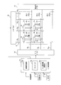
- FIG. 1 is a diagram illustrating a liquid crystal display device according to Embodiment 1 of the present invention.
- FIG. 2 is a diagram for explaining the configuration of the liquid crystal panel shown in FIG.
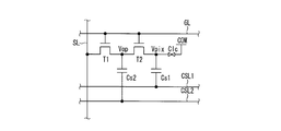
- FIG. 3 is a circuit diagram showing an example of an equivalent circuit of the switching circuit shown in FIG.
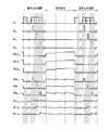
- FIG. 4 is a diagram showing an example of drive signal waveforms of the switching circuit shown in FIG.
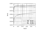
- FIG. 5 is a graph showing a change in off-leakage current of the thin film transistor when the light shielding film is provided and when the light shielding film is not provided.
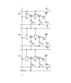
- FIG. 6 is a circuit diagram showing an example of an equivalent circuit of switching circuits arranged in the vertical direction in the active matrix substrate 5.
- FIG. 7 is a diagram showing an example of signal waveforms when the circuit shown in FIG.
- FIG. 8 is driven.
- FIG. 8 is a diagram showing another example of drive signal waveforms in the circuit shown in FIG.
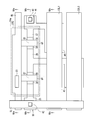
- FIG. 9 is a plan view showing the main structure of the switching circuit.
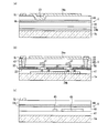
- FIGS. 10A, 10B, and 10C are a cross-sectional view taken along line VIIa-VIIa, a cross-sectional view taken along line VIIb-VIIb, and a cross-sectional view taken along line VIIc-VIIc in FIG. 9, respectively.
- FIG. 11 is a plan view showing a modification of the main structure of the switching circuit.
- FIGS. 10A, 10B, and 10C are a cross-sectional view taken along line VIIa-VIIa, a cross-sectional view taken along line VIIb-VIIb, and a cross-sectional view taken along line VIIc-VIIc in FIG. 9, respectively.
- FIG. 11 is a plan view showing a modification of the main structure of the switching circuit.
- FIG. 12A, 12B, and 12C are a cross-sectional view taken along line VIIa-VIIa, a cross-sectional view taken along line VIIb-VIIb, and a cross-sectional view taken along line VIIc-VIIc in FIG. 11, respectively.
- FIG. 13 is a circuit diagram illustrating an example of an equivalent circuit of the switching circuit according to the second embodiment.
- FIG. 14 is a diagram showing an example of signal waveforms when the circuit shown in FIG. 13 is driven.
- FIG. 15 is a circuit diagram illustrating an example of an equivalent circuit of the switching circuit 18 according to the third embodiment.
- a semiconductor device includes a plurality of switching elements connected in series, one electrode connected to one end side of the plurality of switching elements, and the other electrode connected to a first capacitance control line.
- a light shielding film that blocks light incident on at least one of the plurality of switching elements.
- a light shielding film that blocks light incident on at least one of the plurality of switching elements is formed. Thereby, it is possible to prevent a leakage current due to light from occurring.
- one end side of the plurality of switching elements is connected to the first capacitor wiring via the first capacitor, and the connection point between the adjacent switching elements is connected to the first capacitor via the second capacitor.
- the second capacitor wiring is connected. Due to this configuration, the voltage between adjacent switching elements can be controlled independently of the voltage at one end of the plurality of switching elements. Therefore, the leakage current of the switching element provided between the first capacitor and the second capacitor is controlled by controlling the voltage between the adjacent switching elements using the second capacitor wiring and the second capacitor. It is possible to suppress voltage fluctuations due to.
- a semiconductor device capable of suppressing voltage fluctuation on one end side of the element can be configured.
- the embodiment of the present invention can reliably suppress the leakage current even when a plurality of switching units are connected in series and a capacitor is connected to the connection of the switching elements. Therefore, voltage fluctuations at one end side of the plurality of switching elements can be suppressed.
- the switching element connected between the first capacitor and the second capacitor when the switching element connected between the first capacitor and the second capacitor is OFF, the first capacitor side and the second capacitor in the switching element are turned off.
- the voltage of the second capacitor wiring can be changed so as to reduce the potential difference from the capacitor side. In this way, by controlling the second capacitor wiring, the potential difference between the first capacitor side and the second capacitor side is reduced, and the voltage variation at one end side of the plurality of switching elements due to the leakage current Can be suppressed.
- the switching element connected between the first capacitor and the second capacitor when the switching element connected between the first capacitor and the second capacitor is OFF, the voltage on the second capacitor side is higher than the voltage on the first capacitor side in the switching element.
- the voltage of the second capacitor wiring can be changed so as to increase. Accordingly, when the switching element is OFF, the potential difference can be reduced when the voltage on the second capacitance side becomes lower than the first capacitance side due to leakage current or the like.
- the switching element connected between the first capacitor and the second capacitor is OFF, and immediately before the voltage of the second capacitor wiring is changed, the first capacitor in the switching element is
- the voltage on the second capacitance side can be configured to be lower than the voltage on the capacitance side.
- the voltage on the second capacitance line is changed in a state where the voltage on the second capacitance side is lower than the voltage on the first capacitance side due to leakage current or the like, so that the first capacitance side And the potential difference on the second capacitor side can be reduced.
- the voltage of the second capacitor wiring is 2 at the same time (at a constant time interval). It can be configured to change more than once. In this way, by changing the voltage at regular time intervals, for example, the amount of change in voltage can be made equal, and the voltage adjustment of the second capacitor wiring can be simplified.
- the semiconductor device is configured such that when the switching element connected between the first capacitor and the second capacitor is OFF, the voltage of the second capacitor wiring changes twice or more with the same change amount. be able to. Thereby, the voltage adjustment of the second capacitor wiring can be simplified.
- the semiconductor device is arranged side by side with another semiconductor device, and the second capacitor wiring of the semiconductor device is connected to the switching element of another semiconductor device provided adjacent thereto, and the control of the switching element is performed. It can be set as the aspect which serves as a signal. Thereby, the number of wirings can be reduced.
- the other semiconductor device can have the same structure as the semiconductor device.
- the semiconductor device is provided in each pixel of an active matrix substrate, a pixel electrode is connected to one end side of the plurality of switching elements, and a pixel signal is transmitted to the other end side.
- a signal line for supplying via a switching element can be connected.
- the switching element is turned on when a pixel signal is supplied from the signal line to the pixel electrode, the switching element is turned off, and the voltage of the pixel electrode is to be held.
- the voltage of the second capacitor wiring is changed so as to reduce a potential difference between the pixel electrode side and the signal line side. Thereby, the change in the voltage of the pixel electrode due to the leakage current can be suppressed in the period in which the voltage of the pixel electrode is to be held.
- the switching element is turned on when a pixel signal is supplied from the signal line to the pixel electrode, and the switching element is turned off to hold the voltage of the pixel electrode.
- the voltage of the second capacitor wiring can be changed so that the voltage on the second capacitor side becomes higher than the voltage on the first capacitor side in the switching element.
- the potential difference can be reduced even when the voltage on the first capacitor side becomes lower than that on the second capacitor side due to leakage current or the like in the period in which the voltage of the pixel electrode is to be held.
- the switching element is turned on when a pixel signal is supplied from the signal line to the pixel electrode, and the switching element is turned off to hold the voltage of the pixel electrode.
- the voltage on the second capacitor side may be lower than the voltage on the first capacitor side in the switching element.
- the voltage on the first capacitor side is lower than the second capacitor side due to a leakage current or the like, and the voltage change of the second capacitor wiring The potential difference can be reduced.
- the switching element is turned on when a pixel signal is supplied from the signal line to the pixel electrode, and the switching element is turned off to hold the voltage of the pixel electrode.
- the voltage of the second capacitor wiring can be changed twice or more at the same time. In this way, by changing the voltage at a constant time interval in the period in which the voltage of the pixel electrode should be held, for example, the amount of change in voltage can be made equal, and the voltage adjustment of the second capacitor wiring is simplified. can do.
- the switching element is turned on when a pixel signal is supplied from the signal line to the pixel electrode, and the switching element is turned off to hold the voltage of the pixel electrode.
- the voltage of the second capacitor wiring can be changed twice or more with the same change amount. Thereby, the voltage adjustment of the second capacitor wiring in the period in which the voltage of the pixel electrode should be held can be simplified.
- the switching element is turned on when a pixel signal is supplied from the signal line to the pixel electrode, and holds the voltage of the pixel electrode at which the switching element is turned off.
- the voltage of all the second capacitor wirings formed on the active matrix substrate can be changed at the same timing. Thereby, the pixel driving process of the active matrix substrate can be simplified.
- the switching element is turned on when a pixel signal is supplied from the signal line to the pixel electrode, and holds the voltage of the pixel electrode at which the switching element is turned off.
- the voltages of all the second capacitor wirings formed on the active matrix substrate can be set to the same voltage.
- the pixel driving process of the active matrix substrate can be simplified by controlling the voltages of all the second capacitor wirings to be the same.
- the semiconductor device is provided in each of the pixels arranged in a matrix on the active matrix substrate, and the second capacitor wiring of the semiconductor device provided in the pixel in one row in the matrix is connected to the pixel in the adjacent row. It is possible to adopt a mode that also serves as a scanning line for supplying a control signal to the switching element of the provided semiconductor device. Thereby, the number of wirings provided on the active matrix substrate can be reduced, and the aperture ratio of the pixel can be increased.
- the second capacitor wiring or the first capacitor wiring is formed to extend to a position where light incident on at least one of the plurality of switching elements is blocked, and also serves as the light shielding film It can be.
- the first or second capacitor wiring and the light shielding film can be integrally formed, and the aperture ratio can be improved.
- An active matrix substrate using the semiconductor device is also an embodiment of the present invention.
- a display device including a display unit including the active matrix substrate and a display device in which the display unit is a liquid crystal panel or an organic EL panel are also included in the present invention.
- the display device includes a sensor that detects a state of an ambient environment of the display unit, and a display control unit that performs drive control of the display unit, and the display control unit, based on a detection result from the sensor, A signal adjustment unit that adjusts the frame frequency may be provided.
- the frame frequency of the display image displayed on the display unit can be appropriately adjusted according to the surrounding environment, and a display device having excellent display performance can be easily configured.
- the display device includes a sensor that detects a state of an ambient environment of the display unit, and a display control unit that performs drive control of the display unit, and the display control unit, based on a detection result from the sensor, A signal adjustment unit that adjusts a signal of the second capacitor wiring may be provided.
- FIG. 1 is a diagram illustrating a liquid crystal display device according to Embodiment 1 of the present invention.
- the liquid crystal display device 1 according to the present embodiment includes a liquid crystal panel 2 in which the upper side of FIG. 1 is installed as a viewing side (display surface side), and a non-display surface side of the liquid crystal panel 2 (lower side of FIG. 1).
- a backlight device 3 backlight unit
- the liquid crystal panel 2 constitutes a display unit that displays information.
- the liquid crystal panel 2 includes a color filter substrate 4 (TFT substrate) and an active matrix substrate 5 (counter substrate) constituting a pair of substrates.
- the active matrix substrate 5 and the color filter substrate 4 are disposed to face each other, the peripheral portions of both substrates are bonded with a sealing material, and a liquid crystal layer is provided in a region surrounded by the peripheral portions. That is, a liquid crystal layer (not shown) is sandwiched between the color filter substrate 4 and the active matrix substrate 5.
- Polarizing plates 6 and 7 are provided on the outer surfaces of the color filter substrate 4 and the active matrix substrate 5, respectively. Further, the color filter substrate 4 and the active matrix substrate 5 are made of a transparent transparent resin such as a flat transparent glass material or an acrylic resin. Resin films such as TAC (triacetyl cellulose) or PVA (polyvinyl alcohol) are used for the polarizing plates 6 and 7 and correspond to cover at least the effective display area of the display surface provided in the liquid crystal panel 2. It is bonded to the color filter substrate 4 or the active matrix substrate 5.
- TAC triacetyl cellulose
- PVA polyvinyl alcohol
- the active matrix substrate 5 constitutes one of the pair of substrates.
- pixel electrodes and thin film transistors thin film transistors (in accordance with a plurality of pixels included in the display surface of the liquid crystal panel 2) are provided.
- a TFT (Thin Film Transistor) or the like is formed between the liquid crystal layer (details will be described later).
- the switching circuit (semiconductor device) of the present invention including the thin film transistor is provided for each pixel.
- the color filter substrate 4 constitutes the other of the pair of substrates, and the color filter substrate 4 is formed with a color filter, a counter electrode, and the like between the liquid crystal layer (not shown). )
- the liquid crystal panel 2 is provided with an FPC (Flexible Printed Circuit) 8 connected to a control device (not shown) for controlling the drive of the liquid crystal panel 2 and operates the liquid crystal layer in units of pixels.
- FPC Flexible Printed Circuit
- the display surface is driven in units of pixels and a desired image is displayed on the display surface.
- the liquid crystal mode and pixel structure of the liquid crystal panel 2 are arbitrary. Moreover, the drive mode of the liquid crystal panel 2 is also arbitrary. That is, as the liquid crystal panel 2, any liquid crystal panel that can display information can be used. Therefore, the detailed structure of the liquid crystal panel 2 is not shown in FIG.
- the backlight device 3 includes a light emitting diode 9 as a light source, and a light guide plate 10 disposed to face the light emitting diode 9. Further, in the backlight device 3, the light emitting diode 9 and the light guide plate 10 are sandwiched by the bezel 14 having an L-shaped cross section in a state where the liquid crystal panel 2 is installed above the light guide plate 10. A case 11 is placed on the color filter substrate 4. Thus, the backlight device 3 is assembled to the liquid crystal panel 2 and is integrated as a transmissive liquid crystal display device 1 in which illumination light from the backlight device 3 is incident on the liquid crystal panel 2.
- the light guide plate 10 for example, a synthetic resin such as a transparent acrylic resin is used, and light from the light emitting diode 9 enters.
- a reflection sheet 12 is installed on the opposite side (opposite surface side) of the light guide plate 10 to the liquid crystal panel 2.
- an optical sheet 13 such as a lens sheet or a diffusion sheet is provided on the liquid crystal panel 2 side (light emitting surface side) of the light guide plate 10, and the inside of the light guide plate 10 has a predetermined light guide direction (left side in FIG. 1). The light from the light emitting diode 9 guided in the direction from the right side to the right side is changed to the planar illumination light having uniform luminance and applied to the liquid crystal panel 2.
- the present embodiment is not limited to this, and a direct type backlight device is used. May be.
- a backlight device having other light sources such as a cold cathode fluorescent tube and a hot cathode fluorescent tube other than the light emitting diode can also be used.
- FIG. 2 is a diagram for explaining the configuration of the liquid crystal panel shown in FIG. 2,
- the liquid crystal display device 1 includes a panel control which is an example of a display control unit that performs drive control of the liquid crystal panel 2 (FIG. 1) as the display unit that displays information such as characters and images.
- a source driver 16 and a gate driver 17 that operate based on an instruction signal from the panel control unit 15.
- the liquid crystal display device 1 is provided with a capacitor driver 21 that outputs a predetermined signal to a plurality of capacitors described later. Similar to the source driver 16 and the gate driver 17, the capacitor driver 21 operates based on an instruction signal from the panel control unit 15.
- the panel control unit 15 is provided in the control device, and receives a video signal from the outside of the liquid crystal display device 1. Further, the panel control unit 15 includes a detection result from the temperature sensor TS that detects the ambient temperature of the liquid crystal panel 2 and a detection result from the optical sensor OS that detects the magnitude of external light incident on the liquid crystal panel 2. Is entered.
- the temperature sensor TS and the optical sensor OS are examples of sensors that detect the surrounding environment of the liquid crystal panel (display unit) 2.
- the panel control unit 15 performs predetermined image processing on the input video signal to generate each instruction signal to the source driver 16 and the gate driver 17, and the input video signal.
- a frame buffer 15b capable of storing display data for one frame included, and a signal adjustment unit 15c for adjusting the frame frequency of a display image displayed on the liquid crystal panel 2 are provided. Then, the panel control unit 15 performs drive control of the source driver 16 and the gate driver 17 according to the input video signal, so that information according to the video signal is displayed on the liquid crystal panel 2.
- the signal adjustment unit 15c is configured to adjust the frame frequency based on the detection results of the temperature sensor TS and the optical sensor OS (details will be described later).
- the signal adjustment unit 15c adjusts the voltage of the capacitor controlled by the capacitor driver instead of the frame frequency or in addition to the frame frequency based on the detection results of the temperature sensor TS and the optical sensor OS.
- the frame frequency or the voltage of the capacitor may be adjusted based on the detection results of the temperature sensor TS and the optical sensor OS and the input video signal.
- the source driver 16, the gate driver 17, and the capacitor driver 21 are installed on the active matrix substrate 5. Specifically, the source driver 16 is installed on the surface of the active matrix substrate 5 along the lateral direction of the liquid crystal panel 2 in the outer region of the effective display area A of the liquid crystal panel 2 which is an example of the display panel. ing. Further, the gate driver 17 is installed on the surface of the active matrix substrate 5 so as to be along the vertical direction of the liquid crystal panel 2 in the outer region of the effective display region A. In addition, the capacitor driver 21 is installed on the surface of the active matrix substrate 5 so as to face the gate driver 17 so as to be along the vertical direction of the liquid crystal panel 2 in the outer region of the effective display region A. .
- the configurations of the source driver 16, the gate driver 17, and the capacitor driver 21 are not limited to the above example. For example, at least two of these may be provided concentrated on one side of the effective display area A.
- the source driver 16 and the gate driver 17 are drive circuits that drive a plurality of pixels P provided on the liquid crystal panel 2 side by pixel, and the source driver 16 and the gate driver 17 include a plurality of source electrode lines SL1.
- ⁇ SLm (m is an integer of 2 or more, hereinafter collectively referred to as "SL") and a plurality of gate electrode wirings GL1 to GLn (n is an integer of 2 or more, hereinafter collectively referred to as "GL").
- SL source electrode lines
- GL gate electrode wirings GL1 to GLn
- the source electrode wiring SL and the gate electrode wiring GL constitute a data wiring (signal line) and a scanning wiring (scanning line), respectively, and are made of a transparent glass material or a transparent synthetic resin contained in the active matrix substrate 5.
- the source electrode wiring SL is provided on the substrate so as to be parallel to the matrix column direction (vertical direction of the liquid crystal panel 2), and the gate electrode wiring GL is arranged in the matrix row direction (the liquid crystal panel 2). In the horizontal direction) on the base material.
- the first capacitor lines CSL11 to CSL1n (n is an integer of 2 or more, hereinafter collectively referred to as “CSL1”) and the second capacitor lines CSL21 to CSL2n (hereinafter “ CSL2 ′′ is generally named).
- the first capacitor lines CSL11 to CSL1n are provided in parallel with the second capacitor lines CSL21 to CSL2n, respectively.
- CSL1 and CSL2 are indicated by a single line for the sake of simplicity.
- the first capacitor line CSL1 and the second capacitor line CSL2 are connected to the capacitor driver 21.
- the first capacitor line CSL1 is connected to the pixel electrode of each pixel via the first capacitor.
- the second capacitor line CSL2 is connected via a second capacitor to a connection point between a plurality of thin film transistors connected in series in the switching circuit 18 of each pixel (details will be described later).
- a switching circuit 18 for a pixel electrode (that is, a pixel driving circuit) using the semiconductor device of this embodiment is connected to the switching circuit 18.
- the pixel P having the pixel electrode 19 formed is provided.
- the common electrode 20 is configured to face the pixel electrode 19 with the liquid crystal layer provided on the liquid crystal panel 2 interposed therebetween. That is, in the active matrix substrate 5, the switching circuit 18, the pixel electrode 19, and the common electrode 20 are provided for each pixel.
- the switching circuit 18 has a configuration in which the source and drain of a plurality of thin film transistors are connected in series, and the source electrode wiring SL and the pixel electrode 19 are connected.
- the gates of the plurality of thin film transistors are respectively connected to the gate electrode wiring GL.
- Connection points (nodes) on the plurality of thin film transistors and the pixel electrode side are connected to the first capacitor wiring CSL1 through the first capacitor.
- a connection point between adjacent thin film transistors among the plurality of thin film transistors is connected to the second capacitor wiring CSL2 via the second capacitor.
- at least one of the plurality of thin film transistors of the switching circuit 18 is provided with a light shielding film that blocks light from the backlight. An increase in leakage current of the thin film transistor is suppressed by the light shielding film.
- the switching circuit 18 when a voltage sufficient to cause conduction between the source and the drain is applied to the gates of the plurality of thin film transistors through the gate electrode wiring GL, the source electrode wiring SL, the pixel electrode, and the first electrode The capacitor is electrically connected. Accordingly, when the plurality of thin film transistors are turned on, the pixel electrode and the first capacitor are charged to a predetermined voltage applied from the source electrode line SL. After that, when the gate voltage applied from the gate electrode wiring GL changes and the source and drain of the plurality of thin film transistors become non-conductive (OFF), the source electrode wiring SL, the pixel electrode, and the first capacitor are electrically connected. However, the voltage charged in the pixel electrode and the first capacitor is held.
- the capacitance value of the second capacitor is smaller than the capacitance value of the first capacitor, the drain potential and the source potential of the thin film transistor between the connection point of the first capacitor and the connection point of the second capacitor are Since they are not the same potential, a potential difference occurs. Therefore, in the voltage holding period of the pixel electrode, a voltage is applied through the second capacitor wiring CSL2 so that the potential difference approaches 0. Thereby, the voltage fluctuation of the pixel electrode due to the leakage current is suppressed.
- the gate driver 17 scans the thin film transistors of the corresponding switching circuit 18 with respect to the gate electrode wirings GL1 to GLn based on the instruction signal from the image processing unit 15a. (Gate signal) can be output sequentially. Based on the instruction signal from the image processing unit 15a, the source driver 16 outputs a data signal (voltage signal (gradation voltage)) corresponding to the luminance (gradation) of the display image to the corresponding source electrode wirings SL1 to SLm. can do.
- a data signal voltage signal (gradation voltage)
- the capacitor driver 21 has the first capacitor and the second capacitor in the voltage holding period of the pixel electrode for the capacitor lines CSL11 to CSL1n and CSL21 to CSL2n based on the instruction signal from the image processing unit 15a. A signal for controlling the voltage can be supplied.
- a plurality of pixel P regions are formed in each region partitioned in a matrix by the source electrode wiring SL and the gate electrode wiring GL.
- the plurality of pixels P include red (R), green (G), and blue (B) pixels. These RGB pixels are sequentially arranged in this order, for example, in parallel with the gate electrode lines GL1 to GLn. Further, these RGB pixels can display corresponding colors by a color filter layer (not shown) provided on the color filter substrate 4 side.
- the green pixel can display a green color by arranging a green color filter in a region corresponding to the green pixel of the counter substrate.
- red and blue color filters can be displayed by arranging red and blue color filters in regions corresponding to the respective pixels of the counter substrate.
- the green pixel, the red pixel, and the blue pixel constitute one pixel unit with three colors, thereby enabling color display of an arbitrary color.
- the liquid crystal display device 1 includes a display area formed of a plurality of pixels arranged in a matrix and a driver for driving the display pixels.
- This driver may be formed on the active matrix substrate at the same time, or may be mounted and connected via a terminal region as a driver chip.
- the alignment direction of the liquid crystal material of the liquid crystal layer is controlled for each pixel by turning on and off the thin film transistor.
- the light transmittance of the backlight is controlled for each pixel.
- the transmittance of the backlight light is controlled for each red pixel, green pixel, and blue pixel.
- An image can be displayed on the liquid crystal display panel by displaying the pixel unit with an arbitrary intensity and display color.
- FIG. 3 is a circuit diagram showing an example of an equivalent circuit of the semiconductor device used in the switching circuit 18 shown in FIG.
- the switching circuit 18 includes a first thin film transistor T1 and a second thin film transistor T2 connected in series.
- a MIS (Metal-Insulator-Semiconductor) type transistor can be used for each thin film transistor T1 and T2.
- One end sides of these thin film transistors T1 and T2 are connected to a pixel electrode which is one electrode of the liquid crystal capacitance Clc.
- the liquid crystal capacitor Clc is formed between the pixel electrode and the common electrode COM facing the pixel electrode.
- the other end sides of the thin film transistors T1 and T2 are connected to the source electrode wiring SL.
- the switching circuit 18 further includes a first capacitor Cs1 having one electrode connected to the one end and the other electrode connected to the first capacitor line CSL1.
- the switching circuit 18 includes a second capacitor Cs2 in which one electrode is connected between the adjacent thin film transistors T1 and T2, and the other electrode is connected to the second capacitor line CSL2. That is, the first capacitor Cs1 connected to the pixel electrode side of the thin film transistors T1 and T2 and the second capacitor Cs2 connected between the thin film transistors T1 and T2 are connected to different capacitor lines CSL1 and CSL2, respectively. It becomes the composition. With this configuration, the voltage (Vop) between the two thin film transistors T1 and T2 can be controlled by the signal of the second capacitor wiring CSL2.
- the first capacitor line CSL1 and the second capacitor line CSL2 are two lines whose voltages are controlled independently. Note that the first capacitor wiring can be simply referred to as “first wiring”, and the second capacitor wiring can be referred to as “second wiring” different from the first wiring.
- the voltage value applied to CSL2 is changed at least once during the pixel voltage holding period of the frame period.
- the value of the voltage applied to the capacitor wiring CSL2 is increased by a certain amount three times during one holding period. That is, the voltage of the capacitor line CSL2 is set so that the voltage Vop on the capacitor Cs2 side becomes higher than the voltage Vpix on the capacitor Cs1 side during the holding period in which the source-drain of the thin film transistor T2 between the two capacitors Cs1 and Cs2 is OFF. It is changing.
- the voltage Vop on the side of the capacitor Cs2 is lower than the voltage Vpix on the side of the capacitor Cs1 before the voltage of the capacitor line CSL2 is changed, and the voltage is changed at such a timing that it becomes higher after the voltage change.
- the voltage change of the capacitor wiring CSL2 during the holding period is performed a plurality of times at regular intervals, and the voltage change amount at each time is equal.
- the voltage of the capacitor wiring CSL2 can be controlled using the time interval and the voltage change amount as parameters, and the adjustment becomes easy.
- the direction of change (increase or decrease) of the voltage applied to the capacitor wiring CSL2 during the holding period changes the voltage in a direction in which the potential difference between Vop and Vpix decreases, that is, the potential difference approaches 0. It is preferable.
- control can be performed so that Vop> Vpix immediately after changing the voltage applied to CSL2 during the holding period.
- the charge held in the pixel electrode is only lost during the holding period, but by controlling as in this embodiment, the charge can be supplied to the pixel portion for a certain period during the holding period. It becomes possible.
- the amount and timing of changing the voltage of the capacitor wiring CSL2 in the holding period can be appropriately set according to the characteristics of the switching circuit 18.
- the amount ⁇ CSL2 for changing the voltage of the capacitor wiring CSL2 during the holding period can be calculated using the following equation (1) as an example.
- Cop represents the total sum of the capacitances connected to the node indicated by Vop in FIG. 3 (the node on the line connecting the thin film transistors T1 and T2).
- Cop can be, for example, the sum of Cs2, the gate-drain capacitance of the transistor T1, the gate-source capacitance of the transistor T2, and the parasitic capacitance between each signal wiring (SL, GL, CSL1) and the node.
- Cs2 in the above formula (1) represents the capacitance of the second capacitor Cs2 shown in FIG.
- the voltage value of Vop that changes with time can be reset. Therefore, it is possible to prevent the voltage value of Vop from being separated from the voltage value of Vpix with time and the Vds of the thin film transistor T2 is increased, thereby increasing the off-leakage current. Therefore, it is possible to hold the pixel voltage for a longer time than when this drive is not performed, and it is possible to drive at an extremely low drive frequency. As a result, low power consumption of the display device can be realized.
- a light shielding film is disposed on the thin film transistors T1 and T2 of the switching circuit 18.
- the light-shielding film is preferably provided at a position where the illumination light of the backlight device 3 is blocked so as not to hit the thin film transistor, for example, at a lower portion of the thin film transistor (on the backlight device 3 side). Further, a light shielding film may be provided over the thin film transistor (on the display surface side).
- the light shielding film can prevent the illumination light of the backlight device 3 or the light from the outside of the liquid crystal panel 2 (external light) from directly reaching the channel portions of the thin film transistors T1 and T2. Thereby, an increase in off-leakage current is suppressed.
- FIG. 5 is a graph showing changes in the off-leakage current of the thin film transistor when the light shielding film is provided and when the light shielding film is not provided.
- the vertical axis represents the off-leakage current value (lds) of the thin film transistor
- the horizontal axis represents the source-drain voltage (Vds) of the thin film transistor.
- the off-leakage current of the thin film transistor is reduced by about two digits by providing the light shielding film.
- FIG. 6 is a circuit diagram showing an example of an equivalent circuit of switching circuits arranged in the vertical direction (matrix column direction) of the liquid crystal panel 2 among the switching circuits 18 provided for each pixel in the active matrix substrate 5.
- three switching circuits having the configuration shown in FIG. 3 are arranged in the vertical direction, and these three switching circuits share the source electrode wiring SL extending in the vertical direction.
- FIG. 7 is a diagram showing an example of a signal waveform when the circuit shown in FIG. 6 is driven.
- the gate electrode wiring GLn ⁇ 1 is synchronized with the timings 1,..., N ⁇ 1, n, n + 1 indicating the pixel value applied through the source electrode wiring SL in the writing period.
- GLn, GLn + 1 are applied with voltages for turning on the thin film transistors T1n-1, T2n-1, T1n, T2n, T1n + 1, T2n + 1, respectively.
- the source electrode wiring SL when the voltage of the nth pixel value is applied to the source electrode wiring SL, the ON voltage is applied to the gate electrode wiring GLn, and the thin film transistors T1n and T2n are turned on. Accordingly, the source electrode wiring SL and the pixel electrode are brought into conduction in the pixel in the n-th row, and a predetermined voltage corresponding to the pixel value to be displayed in the liquid crystal capacitor Clcn and the first capacitor Cs1n is charged. That is, the voltage Vpixn of the pixel electrode is a voltage corresponding to the pixel value. At this time, a pulse voltage is also applied to the second capacitor wiring CSL2n in the n-th row, and the voltage Vopn between the two thin film transistors T1 and T2 becomes a predetermined voltage.
- the voltage of the (n + 1) th pixel value is applied to the source electrode wiring SL
- the voltage of the gate electrode wiring GLn returns from the ON voltage to the original, and the ON voltage is applied to the gate electrode wiring GLn + 1 in the (n + 1) th row.
- the pixel voltage holding period starts in the pixels in the n-th row.
- the holding period starts after the end of the writing period, but the starting time of the holding period may be recognized in any way, and is not limited to any one.
- voltage application is repeated for all the rows and columns of the matrix.
- the voltage is changed twice in the capacitor wirings CSL21,..., CSL2n-1, CSL2n, CSL2n + 1 at the same timing.
- the voltages Vopn ⁇ 1, Vopn, and Vopn + 1 between the two thin film transistors T1n ⁇ 1 and T2n ⁇ 1, T1n and T2n, T1n + 1, and T2n + 1 are reset. That is, in the holding period, immediately after resetting Vopn ⁇ 1, Vopn, and Vopn + 1, the voltage of the capacitor wiring CSL2 is controlled so that Vop ⁇ Vpix. Due to the voltage change in the holding period of the capacitor wiring CSL2, the fluctuation due to the leakage current of the voltage Vpixn ⁇ 1, Vpixn, Vpixn + 1 of the pixel electrode of each pixel is suppressed.
- FIG. 8 is a diagram showing another example of drive signal waveforms in the circuit shown in FIG.
- the voltage is changed at the same timing in all the capacitor wirings CSL21,... CSL2n-1, CSL2n, CSL2n + 1 even in the writing period.
- the voltage of all the capacitor wirings CSL21,... CSL2n-1, CSL2n, CSL2n + 1 is set to the low level from the start of pixel writing of the first row to the end of pixel writing of the last row, When the pixel writing of the last row is completed, a predetermined level of voltage is applied.
- FIG. 9 is a plan view showing the main structure of the switching circuit.
- FIGS. 10A, 10B, and 10C are a cross-sectional view taken along line VIIa-VIIa, a cross-sectional view taken along line VIIb-VIIb, and a cross-sectional view taken along line VIIc-VIIc in FIG. 9, respectively.
- the silicon layer SC as a semiconductor layer configured in a substantially linear shape is provided below the gate electrodes g ⁇ b> 1 and g ⁇ b> 3 connected to the gate electrode wiring GL. .
- a light shielding film 24b is formed below the silicon layer SC.
- the light shielding film 24b is provided so as to overlap with the gate electrode wiring GL and the direction perpendicular to the paper surface of FIG. 9 (thickness direction of the active matrix substrate 5). That is, the light shielding film 24b is provided below the gate electrodes g1 and g3 of the thin film transistors T1 and T2, and serves as a lower light shielding film that shields the thin film transistors T1 and T2.
- the light shielding film 24b is preferably formed to extend to a region sufficient to block the backlight irradiation light from entering the channel regions 27 and 35 below the gate electrodes g1 and g3 of the thin film transistors T1 and T2. . For this reason, the light shielding film 24b shown in FIG. 9 is formed not only immediately below the channel regions 27 and 35, but also extending directly below and around the channel regions 27 and 35.
- the upper light shielding film 24a is formed above the silicon layer SC.
- the upper light shielding film 24a is provided so as to cover the thin film transistors T1 and T2. Further, the upper light shielding film 24 is electrically connected to the gate electrode wiring GL through the contact 23.
- a low concentration impurity region (LDD region: Lightly : Doped Drain region) 46 for generating the first capacitor Cs1 and a low concentration impurity region 45 for generating the second capacitor Cs2 extend.
- the low-concentration impurity regions 45 and 46 are provided below the capacitance common lines CSL1 and CSL2, respectively, so that a predetermined capacitance is generated.
- a switching circuit 18 is provided on a substrate body 5a made of a glass substrate for each pixel.
- the light shielding film 24b is formed on the substrate body 5a in the region where the switching circuit 18 is formed.
- a base insulating film 47 is formed so as to cover the light shielding film 24 b and the substrate body 5 a, and a silicon layer SC is provided on the base insulating film 47.
- high-concentration regions shown by cross hatching in FIG. 10) 25, 29, and 37 into which N-type impurities such as phosphorus are implanted at a high concentration, and N-type impurities are implanted at a low concentration.
- Low-concentration impurity regions (LDD regions, indicated by dots in FIG. 10) 26, 28, 34, and 36, and channel regions 27 and 35 formed immediately below the gate electrodes g1 and g3, respectively, are provided. .
- the LDD regions 26, 28, 34, and 36 are arranged so as to sandwich the channel regions 27 and 35 from both sides in the longitudinal direction of the silicon layer SC.
- a gate insulating film 48 is formed so as to cover the silicon layer SC, and gate electrodes g 1 and g 3 are formed on the gate insulating film 48. Thereby, the thin film transistors T1 and T2 are formed as N-type transistors.
- An interlayer film 49 is formed on the gate insulating film 48 so as to cover the gate electrodes g1 and g3.
- the source electrode and the drain electrode 44 formed on the source electrode wiring SL are formed on the interlayer film 49.
- the source electrode is connected to the source region 25 provided in the silicon layer SC through the contact hole 42, and the drain electrode 44 is connected to the drain region 37 provided in the silicon layer SL through the contact hole 43. .
- the upper light shielding film 24 a is provided on the interlayer film 49 so as to be in the same layer as the source electrode and drain electrode 44. As shown in FIG. 10B, the upper light shielding film 24a is provided above the gate electrodes g1 and g3 between the source electrode and the drain electrode 44, and the low-concentration impurity regions 26, 28, and 34 are provided. 36 and the channel regions 27 and 35 are shielded from light. That is, the upper light-shielding film 24a can prevent light from the upper side in FIG. 10B from entering the low-concentration impurity regions 26, 28, 34, and 36 and the channel regions 27 and 35.
- a metal such as molybdenum or tungsten is formed on the substrate body 5a by sputtering, and then patterned by photolithography and etching to form the light shielding film 24b.
- the specific thickness of the light shielding film 24b can be about 100 to 200 nm.
- the base insulating film 47 for example, a SiN film and a SiO 2 film are sequentially formed with a thickness of 100 nm by CVD (Chemical Vapor Deposition). Thereafter, an amorphous silicon film having a thickness of 50 nm is formed above the base insulating film 47, and then polysilicon is formed by laser crystallization. Then, boron is doped into this polysilicon as a channel dope for threshold adjustment.
- CVD Chemical Vapor Deposition
- an SiO 2 film having a thickness of 80 nm is formed as a gate insulating film 48 above the polysilicon, and a metal film such as molybdenum or tungsten is formed above the gate insulating film 48 and patterned. Thereby, the gate electrodes g1 and g3 are formed. Then, in order to form the low-concentration impurity regions 26, 28, 34, and 36 using the gate electrodes g1 and g3 as a mask, an N-type impurity such as phosphorus is doped at a low concentration.
- a photoresist for ensuring the length dimension (LDD length) of the low-concentration impurity regions 26, 28, 34, and 36 is formed, and then the source region 25, the drain region 37, and the high-concentration region 29 are formed.
- LDD length length dimension of the low-concentration impurity regions 26, 28, 34, and 36
- the doping amount is adjusted so that the sheet resistance value is about 50 k ⁇ to 150 k ⁇ (for example, 1 ⁇ 10 13 to 10 14 / cm 2 ). .
- This doping amount is doped so as to cancel the previously doped P-type impurity (boron) for channel doping, and N-type low-concentration impurity regions 26, 28, 34, and 36 are formed.
- phosphorus doping of about 1 ⁇ 10 15 / cm 2 is performed so that the sheet resistance value is 1 k ⁇ or less.
- heat treatment is performed at 500 to 600 ° C. for 1 hour in order to activate the impurities. In order to shorten the heat treatment time, for example, heat treatment may be performed at 650 ° C. to 700 ° C. for several minutes using a lamp annealing apparatus.
- an SiO 2 film and an SiN film are formed to a thickness of about 100 nm to 300 nm, respectively, contact holes 42 and 43 are formed for connection with the source electrode and the drain electrode 44, respectively.
- the drain electrode 44 and a wiring metal, such as Al or an alloy thereof, or a laminated film thereof are formed and patterned.
- the liquid crystal display device 1 forms the pixel electrode 19, and therefore, after forming the wiring, a flattening film made of a resin film or the like is formed, and a transparent film that becomes the pixel electrode 19 is formed thereon.
- An electrode for example, ITO
- Al, Ag, or an alloy thereof is formed on the ITO as a reflective electrode.
- the method of forming the thin film transistors T1 and T2 with N-type transistors has been described.
- the thin film transistors T1 and T2 are formed with P-type transistors, the source region 25 and the drain region are formed.
- the impurity for forming 37 may be a P-type impurity such as boron.
- the switching circuit 18 having this structure can be applied to a switching element that requires a low leakage current.
- the light shielding films 24a and 24b are disposed above and below the thin film transistors T1 and T2.
- the light shielding films 24a and 24b are not necessarily provided on both the thin film transistors T1 and T2.
- an increase in leakage current due to light emitted from the backlight can be suppressed.
- a black matrix formed on a color filter substrate is disposed on top of a thin film transistor. By making this black matrix function as an upper light shielding film, the upper light shielding film 24a shown in FIGS. 9 and 10 can be omitted (see the following modification).
- the active matrix substrate 5 has a semiconductor film, a gate insulating film, a gate signal line, a source signal line, an overcoat film, a planarizing film, It has a structure in which a pixel electrode, an alignment film, and the like are stacked.
- the TFT structure may be a bottom gate type in which the gate signal line is located at the lowermost part, or a top gate type in which the gate signal line is located at the upper part after the semiconductor film is formed first.
- the storage capacitor Cs is formed between the capacitor wiring and the drain electrode on the substrate body, the potential fluctuation of the pixel electrode due to the parasitic capacitance or the off-leak current of the TFT can be suppressed.
- FIG. 11 is a plan view showing a modification of the main structure of the switching circuit.
- FIGS. 12A, 12B, and 12C are a cross-sectional view taken along line VIIa-VIIa, a cross-sectional view taken along line VIIb-VIIb, and a cross-sectional view taken along line VIIc-VIIc in FIG. 11, respectively.
- the upper light shielding film is omitted.
- the capacitor wiring CSL2 is formed in a layer between the switching circuit and the backlight, and extends below the thin film transistors T1 and T2 and is formed as a light shielding film 24b.
- the capacitor wiring CSL2 is formed to extend below the high concentration region 29 of the silicon layer SC connecting the thin film transistors T1 and T2.
- the second capacitor Cs2 is formed by the high concentration region 29, the capacitor wiring CSL2, and the base insulating film 47 therebetween.
- the high concentration region 29 at the connection portion between the thin film transistors T1 and T2 is wider than the other portions, but the high concentration region 29
- the shape and width are not limited to specific ones.
- the area of the high-concentration region 29 can be designed to have a suitable size in order to secure the second capacitor Cs2 in accordance with the dielectric constant, thickness, and the like of the base insulating film 47.
- the capacitor wiring CSL2 is formed so as to overlap at least the channel regions 27 and 35 of the thin film transistors T1 and T2 and the periphery thereof. As a result, the capacitor wiring CSL2 can also serve as the light shielding film 24b. Further, the capacitor wiring CSL2 is formed to extend linearly along the gate electrode wiring GL. In this manner, by forming the capacitor wiring CSL2 at a position overlapping below the gate electrode wiring GL, it is possible to mitigate the decrease in the aperture ratio due to the capacitor wiring CSL2.
- the capacitor wiring CSL2 also serves as the light shielding film 24b.
- the capacitor wiring CSL1 can also serve as the light shielding film 24b.
- the signal adjustment unit 15c is configured to adjust the frame frequency based on the detection results of the temperature sensor TS and the optical sensor OS.
- the leakage current varies depending on the usage environment of the liquid crystal panel 2, that is, the ambient temperature and external light. Therefore, the signal adjustment unit 15c determines the leakage currents of the thin film transistors T1 and T2 based on the detection results of the temperature sensor TS and the optical sensor OS.
- the signal adjustment unit 15c can reduce the frame frequency within a range in which the display image on the liquid crystal panel 2 does not fluctuate by adjusting the frame frequency based on the determination result of the leak current.
- the signal adjustment unit 15c refers to this data, so that the frame frequency corresponding to the detection result of the sensor Can be determined.
- the signal adjustment unit 15c can adjust the frame frequency to be higher as the temperature detected by the temperature sensor TS is higher. Further, the signal adjustment unit 15c can adjust the frame frequency to be higher as the light detected by the optical sensor OS is stronger.
- the signal adjustment unit 15c can also adjust the change amount and change timing of the voltage applied to the second capacitor Cs2 during the holding period according to the detection result of the sensor. For example, the number of voltage changes (voltage gradation) in the holding period can be changed according to the detection result of the sensor. The higher the temperature detected by the temperature sensor TS or the stronger the light detected by the optical sensor OS, the more the number of times can be adjusted or the amount of change in voltage can be adjusted. Also in this case, similarly, data representing a correspondence relationship between the detection value of the sensor and the amount of change or the number of changes of the voltage applied to the capacitor Cs2 is recorded in advance, and the signal adjustment unit 15c refers to this data. Thus, voltage control of the capacitor Cs2 according to the detection result of the sensor can be executed.
- the signal adjustment unit 15c adjusts the voltage control of the frame frequency and / or the capacitance Cs2 based on each detection result of the sensor and / or the input video signal, so that the liquid crystal panel (display unit) 2
- the voltage control of the frame frequency and / or the capacitance Cs2 of the display image displayed at can be adjusted appropriately.
- the liquid crystal display device 1 having excellent display performance can be easily configured.
- the signal adjustment unit 15c can also adjust the frame frequency and the capacity Cs2 control voltage based on the video signal. For example, when the display image (video signal) is a still image, the signal adjustment unit 15c sets the frame frequency to a low frequency equal to or lower than the predetermined frequency, and when the display image is a moving image, The frequency may be a high frequency equal to or higher than a second predetermined frequency (for example, 50 (Hz)).
- a second predetermined frequency for example, 50 (Hz)
- the signal adjustment unit 15c can reduce the power consumption of the liquid crystal panel (display unit) 2 by adjusting the frame frequency to a predetermined frequency or less according to the input video signal. As a result, the power consumption of the liquid crystal display device 1 can be reduced.
- FIG. 13 is a circuit diagram illustrating an example of an equivalent circuit of the switching circuit according to the second embodiment.
- FIG. 13 shows three switching circuits arranged in the vertical direction among the switching circuits of the active matrix substrate 5.
- the three switching circuits shown in FIG. 13 share the source electrode wiring SL extending in the vertical direction.
- the second capacitor wiring CSL2 of each switching circuit is a gate electrode wiring GL of a switching circuit adjacent in the vertical direction.
- the second capacitor line CSL2n connected to the second capacitor Cs2n of the switching circuit in one row in the matrix of the active matrix substrate 5 is used for the ON / OFF control signals of the thin film transistors T1n + 1 and T2n + 2 of the switching circuit in the adjacent row.
- the gate electrode wiring GLn + 1 is also used.
- the second capacitor Cs2 is connected to the second capacitor line CSL2 that is a dedicated control signal line.
- Cs2n is connected to the next-stage gate electrode wiring GLn + 1.
- FIG. 14 is a diagram showing an example of a signal waveform when the circuit shown in FIG. 13 is driven.
- the gate electrode wirings GLn ⁇ 1, GLn, and GLn + 1 apply voltages for turning on the thin film transistors T1n ⁇ 1, T1n, T1n + 1, T2n ⁇ 1, T2n, and T2n + 1 at the respective write timings.
- a voltage is applied so that the voltages Vopn-2, Vopn-1, and Vopn of the nodes connected via the second capacitors Cs2n-2, CS2n-1, and CS2n in the previous stage are set to predetermined voltages.
- the voltage is changed so that Vop ⁇ Vpix immediately after changing the voltage of CSL2 at one or more gradation voltages.
- the capacitor driver 21 shown in FIG. 2 can be omitted.
- FIG. 15 is a circuit diagram illustrating an example of an equivalent circuit of the switching circuit 18 according to the third embodiment.
- the switching circuit 18 includes a plurality (four in this example) of thin film transistors T1a, T1b, T2a, and T2b connected in series.
- the pixel electrode and the source electrode wiring SL are connected via the source and drain of the plurality of thin film transistors T1a, T1b, T2a, and T2b. That is, the pixel electrode is connected to one end of each of the thin film transistors T1a, T1b, T2a, and T2b, and the source wiring electrode SL is connected to the other end.
- the thin film transistors T1a and T1b form a first switching unit SW1, and the thin film transistors T2a and T2b form a second switching unit SW2.
- One electrode of the first capacitor Cs1 is connected to a connection point between the second switching unit SW2 and the pixel electrode.
- the other electrode of the first capacitor Cs1 is connected to the first capacitor line CSL1.
- One electrode of the second capacitor is connected to a connection point between the first switching unit SW1 and the second switching unit SW2.
- the other electrode of the second capacitor Cs2 is connected to the second capacitor line CSL2.
- the gate electrodes g1, g2, g3, and g4 as the top gate electrodes of the thin film transistors T1a, T1b, T2a, and T2b are connected to the gate electrode wiring GL.
- the thin film transistors T2a and T2b of the second switching unit SW2 are double gate transistors having the top gate electrodes (gate electrodes g3 and g4) and the bottom gate electrode 22, respectively.
- the bottom gate electrode 22 is connected to the bottom gate electrode wiring GL ′.
- the bottom gate electrode 22 one that is integrally formed with respect to the two gate electrodes g3 and g4 can be used.
- the bottom gate electrode 22 can be configured to function also as a (lower) light shielding film that shields illumination light from the backlight device 3.
- the bottom light-shielding film 24b shown in FIGS. 9 and 10A is connected to the bottom gate electrode wiring GL ', so that the bottom gate electrode can also serve as the light-shielding film.
- the thin film transistors T2a and T2b use double gate transistors. Therefore, the current driving force (ON current) of the second switching unit SW2 can be easily increased. In addition, since the on-current can be easily increased in this way, it is possible to easily reduce the charging time for the liquid crystal capacitor CLC.
- a portion of a pixel electrode is a region that transmits light, so that a brighter image is obtained as the ratio of the pixel electrode to the total area of the pixel is larger.
- the gate electrode wiring, the source electrode wiring, and the thin film transistor are arranged in the pixel, the area occupied by the pixel electrode is reduced.
- the opening area tends to be further reduced.
- low-frequency drive circuit technologies for reducing power consumption include a configuration in which a memory function such as a conventional DRAM or SRAM method is added to a pixel, a configuration in which a pixel voltage fresh function is added, and the like.
- a memory function such as a conventional DRAM or SRAM method
- a pixel voltage fresh function is added, and the like.
- full color display is difficult and many elements are added, and the pixel aperture ratio is significantly reduced. Therefore, a low frequency driving technique for realizing a high aperture ratio and full color display is very difficult.
- the pixel circuit in the first and second embodiments has a simple configuration in which the pixel circuit is further provided with the light shielding film, the capacitor Cs2, and the capacitor wiring CSL2, so that a high aperture ratio can be realized.
- the voltage value of the Vop shown in FIG. 3 can be suppressed by changing the voltage value of the signal applied to the CSL2 once or more during the pixel voltage holding period.
- fluctuations in the pixel voltage can be suppressed, and low frequency driving can be realized.
- a full color display can be realized. That is, according to the above-described embodiment, it is possible to realize a display that simultaneously satisfies three of the low-frequency driving, the full-color display, and the high aperture ratio, which have been conventionally considered difficult.
- the semiconductor device of the present invention includes a plurality of switching elements connected in series, one electrode connected to one end side of the plurality of switching elements, and the other electrode connected to the first capacitor wiring.
- 1 capacitor, a second capacitor in which one electrode is connected between adjacent switching elements among the plurality of switching elements, and the other electrode is connected to a second capacitor wiring, and the plurality of switching elements There is no limitation as long as it includes a light shielding film that blocks light incident on at least one of the above.
- various display devices such as transflective or reflective liquid crystal panels or organic EL (Electronic Luminescence) elements, inorganic EL elements, field emission displays, and active matrix substrates used therefor Etc.
- the semiconductor device of the present invention can be applied to a switching circuit used in a peripheral circuit such as a driver circuit. Further, the number of switching units connected in series is not limited to the above two to three.
- the switching element of the present invention is not limited to this, for example, an N-type transistor.
- a transistor and a P-type transistor connected in parallel can be used as one switching element.
- the configuration of the switching unit can be simplified, and the semiconductor device can be easily manufactured. It is preferable in that it can be configured.
- the signal adjustment unit has been described with respect to the configuration in which the frame frequency is adjusted using either the detection results of the temperature sensor and the optical sensor or the input video signal.
- the present invention is not limited to this, and any method may be used as long as the frame frequency is adjusted based on at least one of the detection result from the sensor that detects the state of the surrounding environment of the display unit and the input video signal. That is, the signal adjustment unit of the present invention is based on the input video signal in addition to the detection result of the ambient temperature of the display unit from the temperature sensor and the detection result of the external light from the optical sensor to the display unit.
- the frame frequency may be adjusted appropriately by discriminating the magnitude of the leak current at.
- the upper light-shielding film is composed of a conductor and electrically connected to the gate electrode wiring.
- the upper light-shielding film of the present invention is not limited to this. Without being electrically connected to the electrode wiring, the upper light-shielding film may be in a floating state, or the upper light-shielding film may be constituted by a nonconductor.
- the upper light shielding film is formed in the same layer as the source electrode and the drain electrode as in each of the above embodiments, it is preferable that the upper light shielding film is electrically connected to the gate electrode wiring.
- the capacitor of the present invention is limited to this.
- a channel region can be used instead of the low concentration impurity region.
- top gate electrode structure transistor is used
- a bottom gate electrode structure (reverse stagger structure) transistor may be used, and the light shielding film in this case is formed above the transistor.
- This transistor may be a microcrystalline silicon or amorphous silicon transistor as well as a polycrystalline silicon transistor.
- the bottom gate electrode is used as the (lower) light shielding film
- the present invention is not limited to this.
- the bottom gate electrode may be formed using a transparent electrode, and a light shielding film may be provided below the bottom gate electrode below the semiconductor layer.
- a light shielding film made of a nonconductor can be used.
- the present invention even when a plurality of switching parts are connected in series and a capacitor is connected to the connection part of the switching part, leakage current can be reliably suppressed, and one end side of the plurality of switching parts This is useful for a semiconductor device capable of suppressing voltage fluctuations in the semiconductor device, an active matrix substrate using the same, and a display device.
Landscapes
- Physics & Mathematics (AREA)
- Engineering & Computer Science (AREA)
- General Physics & Mathematics (AREA)
- Nonlinear Science (AREA)
- Crystallography & Structural Chemistry (AREA)
- Computer Hardware Design (AREA)
- Theoretical Computer Science (AREA)
- Chemical & Material Sciences (AREA)
- Mathematical Physics (AREA)
- Microelectronics & Electronic Packaging (AREA)
- Optics & Photonics (AREA)
- Liquid Crystal (AREA)
- Signal Processing (AREA)
- Multimedia (AREA)
- Liquid Crystal Display Device Control (AREA)
- Control Of Indicators Other Than Cathode Ray Tubes (AREA)
Abstract
半導体装置は、直列に接続された複数のスイッチング素子(T1)、(T2)と、複数のスイッチング素子(T1)、(T2)の一端側に一方の電極が接続され、他方の電極が第1の容量配線(CSL1)に接続された第1の容量(Cs1)と、複数のスイッチング素子のうち隣り合うスイッチング素子(T1)、(T2)の間に一方の電極が接続され、他方の電極が第2の容量配線(CSL2)に接続された第2の容量(Cs2)と、複数のスイッチング素子(T1)、(T2)の少なくとも1つに対して入射する光を遮る遮光膜とを備える。
Description
本発明は、例えば、トランジスタなどのスイッチング素子を備えた半導体装置、及びこれを用いたアクティブマトリクス基板、並びに表示装置に関する。
近年、例えば液晶表示装置のようなフラットパネルディスプレイは、在来のブラウン管に比べて薄型、軽量などの特長を有する。そのため、液晶テレビ、モニター、携帯電話などに幅広く利用されている。このような液晶表示装置の液晶パネルには、複数のデータ配線(ソース電極配線または信号線とも称される)及び複数の走査配線(ゲート電極配線またはゲート線)がマトリクス状に配線されたアクティブマトリクス基板が用いられる。アクティブマトリクス基板には、データ配線と走査配線との交差部の近傍に設けられる薄膜トランジスタ(TFT:Thin Film Transistor、以下、“TFT”と略称する。)などのスイッチング素子と、このスイッチング素子に接続された画素電極を有する画素が、マトリクス状に配置される。
このように、画素ごとにスイッチング素子を備える表示装置の低消費電力化のためには、駆動周波数を下げることが効果的である。しかし、液晶パネルにおいて、駆動周波数を下げると、液晶画素の電圧保持期間が長くなることにより、保持期間中に液晶画素に印加される電圧を保てなくなり、表示に不具合が発生する。そのため、表示品質を落とさずに、駆動周波数を下げることは困難であった。
液晶画素の電圧変動を抑えるためのTFTの構成例として、液晶画素の一端を、直列に接続された2つのTFTの各ドレイン~ソース間を介して、信号線に接続するとともに、この2つのTFTの各ゲートをそれぞれゲート線に接続する構成が提案されている(例えば、特許文献1参照)。この従来技術では、前記2つのTFT間の接続点に、補助容量の一端を接続し、さらに、液晶画素の他端と、補助容量の他端をそれぞれ接地している。この構成により、TFTの非導通時のリーク電流による液晶画素電圧の変動を抑えることが可能とされていた。
本発明は、複数個のスイッチング部を直列に接続し、かつ、スイッチング素子の接続部に容量を接続した構成において、リーク電流を効果的に抑制することができる半導体装置、及びこれを用いたアクティブマトリクス基板、並びに表示装置を提供することを目的とする。
本発明の一実施形態における半導体装置は、直列に接続された複数のスイッチング素子と、前記複数のスイッチング素子の一端側に一方の電極が接続され、他方の電極が第1の容量制御線に接続された第1の容量と、前記複数のスイッチング素子のうち隣り合うスイッチング素子の間に一方の電極が接続され、他方の電極が第2の容量制御線に接続された第2の容量と、前記複数のスイッチング素子の少なくとも1つに対して入射する光を遮る遮光膜とを備える。
本発明の実施形態によれば、複数個のスイッチング部を直列に接続し、かつ、スイッチング部の接続部に容量を接続したときでも、リーク電流を効果的に抑制することができる半導体装置、及びこれを用いたアクティブマトリクス基板、並びに表示装置を提供することが可能となる。
本発明の一実施形態における半導体装置は、直列に接続された複数のスイッチング素子と、前記複数のスイッチング素子の一端側に一方の電極が接続され、他方の電極が第1の容量制御線に接続された第1の容量と、前記複数のスイッチング素子のうち隣り合うスイッチング素子の間に一方の電極が接続され、他方の電極が第2の容量制御線に接続された第2の容量と、前記複数のスイッチング素子の少なくとも1つに対して入射する光を遮る遮光膜とを備える。
上記のように構成された半導体装置では、複数のスイッチング素子の少なくとも1つに対して入射する光を遮る遮光膜が形成されている。これにより、光によるリーク電流が発生するのを防ぐことができる。
さらに、上記半導体装置では、複数のスイッチング素子の一端側は、第1の容量を介して第1の容量配線に接続され、隣り合うスイッチング素子の間の接続点には、第2の容量を介して第2の容量配線が接続されている。この構成のため、隣り合うスイッチング素子の間における電圧を、複数のスイッチング素子の一端側の電圧とは独立して制御することが可能になる。そのため、第2の容量配線及び第2の容量を用いて、隣り合うスイッチング素子の間における電圧を制御することにより、第1の容量と第2の容量の間に設けられたスイッチング素子のリーク電流による電圧の変動を抑えることが可能になる。
この結果、上記従来例と異なり、複数個のスイッチング素子を直列に接続し、かつ、スイッチング素子の接続部に容量を接続したときでも、リーク電流を確実に抑制することができ、複数個のスイッチング素子の一端部側での電圧変動を抑えることができる半導体装置を構成することができる。
例えば、上記従来技術でも、駆動周波数を下げた場合に、リーク電流を十分に抑えることは困難であった。スイッチング素子として低温ポリシリコンTFTを用いた液晶パネルにおいて駆動周波数を下げると、保持期間中に液晶に印加される電圧を保てなくなり、表示に不具合が発生する。
また、上記従来技術のように、2つのスイッチング部SW1及びSW2を直列に接続し、かつ、SW1及びSW2の接続部に容量を接続したときでも、低周波駆動を行い保持期間が長くなるにつれ、SW1のオフリークによって、SW1とSW2の接続部分の電圧が徐々に変化してしまう。そのため、SW2のオフリーク電流が時間と共に増加し、それにともなって液晶印加電圧が変化してしまう。従って、極めて低い駆動周波数での動作は困難である。
これに対して、本発明の実施形態は、複数個のスイッチング部を直列に接続し、かつ、スイッチング素子の接続部に容量を接続したときでも、リーク電流を確実に抑制することができる。そのため、複数個のスイッチング素子の一端部側での電圧変動を抑えることができる。
本発明の実施形態における上記半導体装置において、前記第1の容量と第2の容量の間に接続されたスイッチング素子がOFFのときに、当該スイッチング素子において前記第1の容量側と前記第2の容量側との電位差を少なくするよう前記第2の容量配線の電圧を変化させることができる。このように、第2の容量配線を制御することで、前記第1の容量側と前記第2の容量側との電位差を少なくし、リーク電流による、複数のスイッチング素子の一端側の電圧の変動を抑えることができる。
上記半導体装置は、前記第1の容量と第2の容量の間に接続されたスイッチング素子がOFFのときに、当該スイッチング素子において前記第1の容量側の電圧より前記第2の容量側の電圧が高くなるよう前記第2の容量配線の電圧を変化させるよう構成することができる。これにより、前記スイッチング素子がOFFのときに、リーク電流等により、第1の容量側より第2の容量側の電圧が低くなった場合に、電位差を少なくすることができる。
上記半導体装置は、前記第1の容量と第2の容量の間に接続されたスイッチング素子がOFFであり、前記第2の容量配線の電圧を変化させる直前において、当該スイッチング素子における前記第1の容量側の電圧より前記第2の容量側の電圧が低くなるよう構成することができる。これにより、リーク電流等のために第1の容量側の電圧より第2の容量側の電圧が低くなった状態で、前記第2の容量配線の電圧を変化させることで、第1の容量側と第2の容量側の電位差を少なくすることができる。
上記半導体装置は、前記第1の容量と第2の容量の間に接続されたスイッチング素子がOFFのときに、前記第2の容量配線の電圧が同一時間毎(一定の時間間隔で)に2回以上変化するよう構成することができる。このように一定時間間隔で電圧を変化させることで、例えば、各回の電圧の変化量を等しくすることができ、前記第2の容量配線の電圧調整を単純化することができる。
上記半導体装置は、前記第1の容量と第2の容量の間に接続されたスイッチング素子がOFFのときに、前記第2の容量配線の電圧が同一変化量で2回以上変化するよう構成することができる。これにより、前記第2の容量配線の電圧調整を単純化することができる。
前記半導体装置は、他の半導体装置とともに並べて配置されており、前記半導体装置の前記第2の容量配線は、隣接して設けられる他の半導体装置の前記スイッチング素子へ接続され、当該スイッチング素子の制御信号を兼ねている態様とすることができる。これにより、配線の数を少なくすることができる。ここで、他の半導体装置は、上記半導体装置と同様の構成とすることができる。
前記半導体装置は、実施形態の一つとして、アクティブマトリクス基板の各画素に設けられ、前記複数のスイッチング素子の一端側には、画素電極が接続され、他端側には画素信号を前記複数のスイッチング素子を介して供給するための信号線が接続される態様とすることができる。
このように、前記半導体装置をアクティブマトリクス基板の各画素に設けることより、スイッチング素子を介して画素電極に書き込まれた電荷がリーク電流によって時間と共に失われてしまうことを抑制できる。その結果、アクティブマトリクス基板を用いた表示装置の駆動周波数を下げ、低消費電力化を図りつつ、良好な表示を維持することができる。
前記アクティブマトリクス基板の半導体装置において、前記スイッチング素子は、前記信号線から画素電極へ画素信号が供給される際にONとなり、前記スイッチング素子がOFFとなり、前記画素電極の電圧を保持すべき期間において、当該スイッチング素子において前記画素電極側と、前記信号線側の電位差を少なくするよう前記第2の容量配線の電圧を変化させることが好ましい。これにより、画素電極の電圧を保持すべき期間において、リーク電流による画素電極の電圧の変化を抑えることができる。
上記アクティブマトリクス基板に設けられた半導体装置において、前記スイッチング素子は、前記信号線から画素電極へ画素信号が供給される際にONとなり、前記スイッチング素子がOFFとなり、前記画素電極の電圧を保持すべき期間において、当該スイッチング素子において前記第1の容量側の電圧より前記第2の容量側の電圧が高くなるよう前記第2の容量配線の電圧を変化させる構成とすることができる。これにより、前記画素電極の電圧を保持すべき期間において、リーク電流等のために第1の容量側の電圧が第2の容量側より低くなった場合にも、電位差を少なくすることができる。
上記アクティブマトリクス基板に設けられた半導体装置において、前記スイッチング素子は、前記信号線から画素電極へ画素信号が供給される際にONとなり、前記スイッチング素子がOFFとなり、前記画素電極の電圧を保持すべき期間において、前記第2の容量配線の電圧を変化させる直前において、当該スイッチング素子における前記第1の容量側の電圧より前記第2の容量側の電圧が低くなる構成とすることができる。これにより、前記画素電極の電圧を保持すべき期間において、リーク電流等のために第1の容量側の電圧が第2の容量側より低くなった状態で、第2の容量配線の電圧変化により、電位差を少なくすることができる。
上記アクティブマトリクス基板に設けられた半導体装置において、前記スイッチング素子は、前記信号線から画素電極へ画素信号が供給される際にONとなり、前記スイッチング素子がOFFとなり、前記画素電極の電圧を保持すべき期間において、前記第2の容量配線の電圧が同一時間毎に2回以上変化する構成とすることができる。このように画素電極の電圧を保持すべき期間において一定時間間隔で電圧を変化させることで、例えば、各回の電圧の変化量を等しくすることができ、第2の容量配線の電圧調整を単純化することができる。
上記アクティブマトリクス基板に設けられた半導体装置において、前記スイッチング素子は、前記信号線から画素電極へ画素信号が供給される際にONとなり、前記スイッチング素子がOFFとなり、前記画素電極の電圧を保持すべき期間において、前記第2の容量配線の電圧が同一変化量で2回以上変化する構成とすることができる。これにより、画素電極の電圧を保持すべき期間における第2の容量配線の電圧調整を単純化することができる。
上記アクティブマトリクス基板に設けられた半導体装置において、前記スイッチング素子は、前記信号線から画素電極へ画素信号が供給される際にONとなり、前記スイッチング素子がOFFとなる前記画素電極の電圧を保持すべき期間において、前記アクティブマトリクス基板上に形成される全ての第2の容量配線の電圧を同じタイミングで変化させる構成とすることができる。これにより、アクティブマトリクス基板の画素駆動処理を単純化することができる。
上記アクティブマトリクス基板に設けられた半導体装置において、前記スイッチング素子は、前記信号線から画素電極へ画素信号が供給される際にONとなり、前記スイッチング素子がOFFとなる前記画素電極の電圧を保持すべき期間において、前記アクティブマトリクス基板上に形成される全ての第2の容量配線の電圧を同一の電圧にすることができる。このように画素電極の電圧を保持すべき期間中、全ての第2の容量配線の電圧が同一になるよう制御することで、アクティブマトリクス基板の画素駆動処理を単純化することができる。
前記半導体装置は、アクティブマトリクス基板にマトリクス状に配置された画素の各々に設けられ、マトリクスにおける1つの行の画素に設けられた半導体装置の前記第2の容量配線は、隣接する行の画素に設けられた半導体装置のスイッチング素子へ制御信号を供給する走査線を兼ねている態様とすることができる。これにより、アクティブマトリクス基板に設ける配線数を少なくし、画素の開口率をより大きくできる。
前記半導体装置において、記第2の容量配線または前記第1の容量配線が、前記複数のスイッチング素子の少なくとも1つに対して入射する光を遮る位置まで延びて形成され、前記遮光膜を兼ねる構成とすることができる。これにより、第1または第2の容量配線と遮光膜とを一体的に形成することができ、開口率を向上させることができる。
前記半導体装置を用いたアクティブマトリクス基板も本発明の一実施形態である。また、前記アクティブマトリクス基板を含む表示部を備えた表示装置、並びに、前記表示部が液晶パネルまたは有機ELパネルである表示装置も、本発明に含まれる。
前記表示装置は、前記表示部の周囲環境の状態を検出するセンサーと、前記表示部の駆動制御を行う表示制御部を備え、前記表示制御部には、前記センサーからの検出結果に基づいて、フレーム周波数を調整する信号調整部が設けられてもよい。
これにより、表示部で表示される表示画像のフレーム周波数を、周囲環境に応じて適切に調整することができ、優れた表示性能を有する表示装置を容易に構成することができる。
前記表示装置は、前記表示部の周囲環境の状態を検出するセンサーと、前記表示部の駆動制御を行う表示制御部を備え、前記表示制御部には、前記センサーからの検出結果に基づいて、前記第2の容量配線の信号を調整する信号調整部が設けられてもよい。
これにより、第2の容量配線の信号を適切に調整することができ、周囲環境に応じたリーク電流の適切な抑制が可能になる。その結果、優れた表示性能を有する表示装置を容易に構成することができる。
以下、本発明の半導体装置、アクティブマトリクス基板、及び表示装置の実施形態について、図面を参照しながら説明する。尚、以下の説明では、本発明を、液晶パネルのアクティブマトリクス基板に用いられる画素電極用のスイッチング回路に適用した場合を例示して説明する。また、各図中の構成部材の寸法は、実際の構成部材の寸法及び各構成部材の寸法比率等を忠実に表したものではない。
[実施形態1]
(液晶表示装置の構成例)
図1は、本発明の実施形態1にかかる液晶表示装置を説明する図である。図1において、本実施形態の液晶表示装置1は、図1の上側が視認側(表示面側)として設置される液晶パネル2と、液晶パネル2の非表示面側(図1の下側)に配置されて、当該液晶パネル2を照明する照明光を発生するバックライト装置3(バックライトユニット)とが設けられている。液晶パネル2は、情報を表示する表示部を構成している。
(液晶表示装置の構成例)
図1は、本発明の実施形態1にかかる液晶表示装置を説明する図である。図1において、本実施形態の液晶表示装置1は、図1の上側が視認側(表示面側)として設置される液晶パネル2と、液晶パネル2の非表示面側(図1の下側)に配置されて、当該液晶パネル2を照明する照明光を発生するバックライト装置3(バックライトユニット)とが設けられている。液晶パネル2は、情報を表示する表示部を構成している。
液晶パネル2は、一対の基板を構成するカラーフィルタ基板4(TFT基板)及びアクティブマトリクス基板5(対向基板)を備える。アクティブマトリクス基板5と、カラーフィルタ基板4とが対向配置されており、両基板の周縁部はシール材で接着され、その周縁部に囲まれた領域に液晶層が設けられている。すなわち、カラーフィルタ基板4とアクティブマトリクス基板5との間には、図示を省略した液晶層が狭持されている。
カラーフィルタ基板4及びアクティブマトリクス基板5の各外側表面にそれぞれ偏光板6、7が設けられている。また、カラーフィルタ基板4及びアクティブマトリクス基板5には、平板状の透明なガラス材またはアクリル樹脂などの透明な合成樹脂が使用されている。偏光板6、7には、TAC(トリアセチルセルロース)またはPVA(ポリビニルアルコール)などの樹脂フィルムが使用されており、液晶パネル2に設けられた表示面の有効表示領域を少なくとも覆うように対応するカラーフィルタ基板4またはアクティブマトリクス基板5に貼り合わせられている。
また、アクティブマトリクス基板5は、上記一対の基板の一方の基板を構成するものであり、アクティブマトリクス基板5では、液晶パネル2の表示面に含まれる複数の画素に応じて、画素電極や薄膜トランジスタ(TFT:Thin Film Transistor)などが上記液晶層との間に形成されている(詳細は後述。)。また、このアクティブマトリクス基板5では、後に詳述するように、上記薄膜トランジスタを含んだ本発明のスイッチング回路(半導体装置)が、画素単位に設けられている。一方、カラーフィルタ基板4は、一対の基板の他方の基板を構成するものであり、カラーフィルタ基板4には、カラーフィルタや対向電極などが上記液晶層との間に形成されている(図示せず)。
また、液晶パネル2では、当該液晶パネル2の駆動制御を行う制御装置(図示せず)に接続されたFPC(Flexible Printed Circuit)8が設けられており、上記液晶層を画素単位に動作することで表示面を画素単位に駆動して、当該表示面上に所望画像を表示するようになっている。
尚、液晶パネル2の液晶モードや画素構造は任意である。また、液晶パネル2の駆動モードも任意である。すなわち、液晶パネル2としては、情報を表示できる任意の液晶パネルを用いることができる。それ故、図1においては液晶パネル2の詳細な構造を図示せず、その説明も省略する。
バックライト装置3は、光源としての発光ダイオード9と、発光ダイオード9に対向して配置された導光板10とを備えている。また、バックライト装置3では、断面L字状のベゼル14により、導光板10の上方に液晶パネル2が設置された状態で、発光ダイオード9及び導光板10が狭持されている。また、カラーフィルタ基板4には、ケース11が載置されている。これにより、バックライト装置3は、液晶パネル2に組み付けられて、当該バックライト装置3からの照明光が液晶パネル2に入射される透過型の液晶表示装置1として一体化されている。
導光板10には、例えば透明なアクリル樹脂などの合成樹脂が用いられており、発光ダイオード9からの光が入光される。導光板10の液晶パネル2と反対側(対向面側)には、反射シート12が設置されている。また、導光板10の液晶パネル2側(発光面側)には、レンズシートや拡散シートなどの光学シート13が設けられており、導光板10の内部を所定の導光方向(図1の左側から右側への方向)に導かれた発光ダイオード9からの光が均一な輝度をもつ平面状の上記照明光に変えられて液晶パネル2に与えられる。
尚、上記の説明では、導光板10を有するエッジライト型のバックライト装置3を用いた構成について説明したが、本実施形態はこれに限定されるものではなく、直下型のバックライト装置を用いてもよい。また、発光ダイオード以外の冷陰極蛍光管や熱陰極蛍光管などの他の光源を有するバックライト装置も用いることができる。
(液晶パネルの構成例)
図2は、図1に示した液晶パネルの構成を説明する図である。図2において、液晶表示装置1(図1)には、文字や画像等の情報を表示する上記表示部としての液晶パネル2(図1)の駆動制御を行う表示制御部の一例であるパネル制御部15と、このパネル制御部15からの指示信号を基に動作するソースドライバ16及びゲートドライバ17が設けられている。また、液晶表示装置1には、後述の複数個の容量に対して、所定の信号を出力する容量用ドライバ21が設けられている。この容量用ドライバ21は、ソースドライバ16及びゲートドライバ17と同様に、パネル制御部15からの指示信号に基づき動作するようになっている。
図2は、図1に示した液晶パネルの構成を説明する図である。図2において、液晶表示装置1(図1)には、文字や画像等の情報を表示する上記表示部としての液晶パネル2(図1)の駆動制御を行う表示制御部の一例であるパネル制御部15と、このパネル制御部15からの指示信号を基に動作するソースドライバ16及びゲートドライバ17が設けられている。また、液晶表示装置1には、後述の複数個の容量に対して、所定の信号を出力する容量用ドライバ21が設けられている。この容量用ドライバ21は、ソースドライバ16及びゲートドライバ17と同様に、パネル制御部15からの指示信号に基づき動作するようになっている。
パネル制御部15は、上記制御装置内に設けられたものであり、液晶表示装置1の外部からの映像信号が入力されるようになっている。また、パネル制御部15には、液晶パネル2の周囲温度を検出する温度センサーTSからの検出結果と、液晶パネル2に入光される外光の大きさを検出する光センサーOSからの検出結果が入力されるようになっている。これら温度センサーTS及び光センサーOSは、液晶パネル(表示部)2の周囲環境を検出するセンサーの一例である。
また、パネル制御部15は、入力された映像信号に対して所定の画像処理を行ってソースドライバ16及びゲートドライバ17への各指示信号を生成する画像処理部15aと、入力された映像信号に含まれた1フレーム分の表示データを記憶可能なフレームバッファ15bと、液晶パネル2に表示される表示画像のフレーム周波数を調整する信号調整部15cを備えている。そして、パネル制御部15が、入力された映像信号に応じて、ソースドライバ16及びゲートドライバ17の駆動制御を行うことにより、その映像信号に応じた情報が液晶パネル2に表示される。
また、信号調整部15cは、温度センサーTS及び光センサーOSの各検出結果に基づいて、上記フレーム周波数を調整するように構成されている(詳細は後述。)。尚、信号調整部15cは、温度センサーTS及び光センサーOSの各検出結果に基づいて、上記フレーム周波数の代わりに、またはフレーム周波数に加えて、容量用ドライバで制御される容量の電圧を調整してもよいし、温度センサーTS及び光センサーOSの各検出結果及び入力された映像信号に基づいて、上記フレーム周波数または上記容量の電圧を調整するよう構成されてもよい。
ソースドライバ16、ゲートドライバ17、容量用ドライバ21は、アクティブマトリクス基板5上に設置されている。具体的には、ソースドライバ16は、アクティブマトリクス基板5の表面上において、表示パネルの一例である液晶パネル2の有効表示領域Aの外側領域で当該液晶パネル2の横方向に沿うように設置されている。また、ゲートドライバ17は、アクティブマトリクス基板5の表面上において、上記有効表示領域Aの外側領域で当該液晶パネル2の縦方向に沿うように設置されている。また、容量用ドライバ21は、アクティブマトリクス基板5の表面上において、ゲートドライバ17と対向するように、上記有効表示領域Aの外側領域で当該液晶パネル2の縦方向に沿うように設置されている。なお、ソースドライバ16、ゲートドライバ17及び容量用ドライバ21の構成は上記例に限られない。例えば、これら少なくとも2つを有効表示領域Aの1つの辺側に集中して設けてもよい。
また、ソースドライバ16及びゲートドライバ17は、液晶パネル2側に設けられた複数の画素Pを画素単位に駆動する駆動回路であり、ソースドライバ16及びゲートドライバ17には、複数のソース電極配線SL1~SLm(mは、2以上の整数、以下、“SL”にて総称する。)及び複数のゲート電極配線GL1~GLn(nは、2以上の整数、以下、“GL”にて総称する。)がそれぞれ接続されている。これらのソース電極配線SL及びゲート電極配線GLは、それぞれデータ配線(信号線)及び走査配線(走査線)を構成しており、アクティブマトリクス基板5に含まれた透明なガラス材または透明な合成樹脂製の基材(図示せず)上で互いに交差するように、マトリクス状に配列されている。すなわち、ソース電極配線SLは、マトリクス状の列方向(液晶パネル2の縦方向)に平行となるように上記基材上に設けられ、ゲート電極配線GLは、マトリクス状の行方向(液晶パネル2の横方向)に平行となるように上記基材上に設けられている。
また、アクティブマトリクス基板5では、第1の容量配線CSL11~CSL1n(nは、2以上の整数、以下、“CSL1”にて総称する。)、及び第2の容量配線CSL21~CSL2n(以下、“CSL2”にて総称する。)が設けられる。第1の容量配線CSL11~CSL1nは、第2の容量配線CSL21~CSL2nと、それぞれ平行になるように設けられる。尚、図2では、図を簡単にするため、CSL1とCSL2を1本の線で示している。これらの第1の容量配線CSL1及び第2の容量配線CSL2は、容量用ドライバ21に接続されている。さらに、第1の容量配線CSL1は、各画素の画素電極に第1の容量を介して接続される。第2の容量配線CSL2は、各画素のスイッチング回路18において直列に接続された複数の薄膜トランジスタの間の接続点に、第2の容量を介して接続される(詳細は後述。)。
ソース電極配線SLと、ゲート電極配線GLとの交差部の近傍には、本実施形態の半導体装置を用いた画素電極用(つまり、画素駆動回路用)のスイッチング回路18と、スイッチング回路18に接続された画素電極19を有する上記画素Pが設けられている。また、各画素Pでは、共通電極20が液晶パネル2に設けられた上記液晶層を間に挟んだ状態で画素電極19に対向するよう構成されている。すなわち、アクティブマトリクス基板5では、スイッチング回路18、画素電極19、及び共通電極20が画素単位に設けられている。
スイッチング回路18は、複数の薄膜トランジスタのソース-ドレイン間を直列に接続したもので、ソース電極配線SLと画素電極19とを繋ぐ構成となっている。複数の薄膜トランジスタのゲートは、それぞれ、ゲート電極配線GLに接続される。複数の薄膜トランジスタと画素電極側の接続点(ノード)は第1の容量を介して第1の容量配線CSL1に接続される。複数の薄膜トランジスタのうち、隣り合う薄膜トランジスタ間の接続点は、第2の容量を介して、第2の容量配線CSL2に接続される。また、スイッチング回路18の複数の薄膜トランジスタの少なくとも1つには、バックライトからの光を遮断する遮光膜が設けられる。遮光膜により薄膜トランジスタのリーク電流の増大が抑制される。
スイッチング回路18において、複数の薄膜トランジスタのゲートに、ゲート電極配線GLを介して、ソース-ドレイン間が導通するのに十分な電圧が印加されると、ソース電極配線SLと、画素電極及び第1の容量とが電気的に接続される。これにより、複数の薄膜トランジスタがONになると、画素電極と第1の容量とはソース電極線SLから印加された所定の電圧に充電される。その後、ゲート電極配線GLから印加されるゲート電圧が変化して、複数の薄膜トランジスタのソース-ドレイン間が非導通(OFF)になると、ソース電極配線SLと画素電極及び第1の容量とは電気的に切り離されるが、画素電極及び第1の容量に充電された電圧は保持される。このとき、第1の容量の容量値に比べ第2の容量の容量値が小さい場合、第1の容量の接続点と第2の容量の接続点との間の薄膜トランジスタのドレイン電位とソース電位は同電位とはならないため、電位差が生じることになる。そこで、画素電極の電圧保持期間において、第2の容量配線CSL2を介して、上記電位差を0に近づけるよう電圧が印加される。これにより、リーク電流による画素電極の電圧変動が抑えられる。
上記の駆動を実現するために、ゲートドライバ17は、画像処理部15aからの指示信号に基づいて、ゲート電極配線GL1~GLnに対して、対応するスイッチング回路18の薄膜トランジスタをON状態にする走査信号(ゲート信号)を順次出力することができる。ソースドライバ16は、画像処理部15aからの指示信号に基づいて、表示画像の輝度(階調)に応じたデータ信号(電圧信号(階調電圧))を対応するソース電極配線SL1~SLmに出力することができる。
また、容量用ドライバ21は、画像処理部15aからの指示信号に基づいて、容量配線CSL11~CSL1n及びCSL21~CSL2nに対して、画素電極の電圧保持期間における第1の容量と第2の容量の電圧を制御する信号を供給することができる。
さて、アクティブマトリクス基板5では、ソース電極配線SLと、ゲート電極配線GLとによってマトリクス状に区画された各領域に、複数の各画素Pの領域が形成されている。これら複数の画素Pには、赤色(R)、緑色(G)、及び青色(B)の画素が含まれている。また、これらのRGBの画素は、例えばこの順番で、各ゲート電極配線GL1~GLnに平行に順次配設されている。さらに、これらのRGBの画素は、カラーフィルタ基板4側に設けられたカラーフィルタ層(図示せず)により、対応する色の表示を行えるようになっている。
緑色画素は、対向基板の緑色画素に対応する領域に緑色のカラーフィルタが配置されることにより、緑色を表示することができるものである。赤色画素、青色画素についても同様に、対向基板の各画素に対応する領域に赤色、青色のカラーフィルタが配置されることにより、赤色及び青色を表示することができるものである。緑色画素、赤色画素、及び青色画素は、3色で1つの画素ユニットを構成し、これにより、任意の色のカラー表示を行うことができる。
上記のように、液晶表示装置1は、マトリクス状に配置された複数の画素で形成された表示領域と、表示画素を駆動するためのドライバを備えている。このドライバは、アクティブマトリクス基板上に同時に形成してもよいし、あるいはドライバチップとして端子領域を介して実装接続してもよい。
以上の構成の液晶表示装置1では、薄膜トランジスタのオン・オフにより、画素毎に液晶層の液晶材料の配向方向が制御される。これにより、画素毎に、バックライトの光の透過率が制御される。例えば、各赤色画素、緑色画素、及び青色画素毎にバックライト光の透過率の制御がなされる。画素ユニットで任意の強度及び表示色で表示を行うことにより、液晶表示パネルにおいて任意の画像を表示することができる。
(スイッチング回路の構成例及び動作例)
図3は、図2に示したスイッチング回路18に用いられる半導体装置の等価回路の一例を示す回路図である。図3に示す例では、スイッチング回路18は、直列に接続された第1の薄膜トランジスタT1及び第2の薄膜トランジスタT2を備える。各薄膜トランジスタT1及びT2には、例えば、MIS(Metal-Insulator-Semiconductor)型のトランジスタを用いることができる。これらの薄膜トランジスタT1及びT2の一端側は、液晶容量Clcの一方の電極である画素電極に接続されている。液晶容量Clcは、この画素電極と対向する共通電極COMとの間に形成される。薄膜トランジスタT1及びT2の他端側は、ソース電極配線SLに接続されている。
図3は、図2に示したスイッチング回路18に用いられる半導体装置の等価回路の一例を示す回路図である。図3に示す例では、スイッチング回路18は、直列に接続された第1の薄膜トランジスタT1及び第2の薄膜トランジスタT2を備える。各薄膜トランジスタT1及びT2には、例えば、MIS(Metal-Insulator-Semiconductor)型のトランジスタを用いることができる。これらの薄膜トランジスタT1及びT2の一端側は、液晶容量Clcの一方の電極である画素電極に接続されている。液晶容量Clcは、この画素電極と対向する共通電極COMとの間に形成される。薄膜トランジスタT1及びT2の他端側は、ソース電極配線SLに接続されている。
スイッチング回路18は、さらに、前記一端側に一方の電極が接続され、他方の電極が第1の容量配線CSL1に接続された第1の容量Cs1を備える。また、スイッチング回路18は、隣り合う薄膜トランジスタT1及びT2の間に一方の電極が接続され、他方の電極が第2の容量配線CSL2に接続された第2の容量Cs2を備える。すなわち、薄膜トランジスタT1及びT2の画素電極側に接続された第1の容量Cs1と、薄膜トランジスタT1及びT2の間に接続された第2の容量Cs2が、それぞれ、別の容量配線CSL1及びCSL2に接続された構成となっている。この構成により、2つの薄膜トランジスタT1及びT2の間の電圧(Vop)を第2の容量配線CSL2の信号によって制御することが可能となる。例えば、画素電極の電圧保持期間に、Vopを制御して、Vopの電圧値をVpix相当とすることで、薄膜トランジスタT2のVds(ドレイン-ソース間の電位差)を小さくし、リーク電流を小さくすることができる。このように、本実施形態において、第1の容量配線CSL1と第2の容量配線CSL2は、それぞれ独立して電圧が制御される2つの配線である。なお、第1の容量配線を単に「第1の配線」と称し、第2の容量配線は、第1の配線とは異なる「第2の配線」と称することができる。
具体的には、図4に示すように、フレーム周期の画素電圧保持期間中にCSL2に与える電圧値を少なくとも1回変化させる。図4に示す例では、1周期の保持期間において、3回、容量配線CSL2に印加する電圧の値を一定量上げている。すなわち、2つの容量Cs1及びCs2間の薄膜トランジスタT2のソース-ドレイン間がOFFである保持期間に、容量Cs2側の電圧Vopが、容量Cs1側の電圧Vpixより高くなるよう、容量配線CSL2の電圧を変化させている。また、容量配線CSL2の電圧変化前は容量Cs2側の電圧Vopは容量Cs1側の電圧Vpixより低く、電圧変化後に高くなるようなタイミングで、電圧を変化させている。
さらに、図4に示す例では、保持期間における容量配線CSL2の電圧変化は、一定の間隔で複数回行われており、かつ、各回の電圧変化量は等しくなっている。これにより、例えば、時間間隔と電圧変化量とをパラメータとして、容量配線CSL2の電圧を制御することができ、調整が容易になる。
ここで、保持期間における容量配線CSL2への印加電圧の変化の方向(増加か減少か)は、VopとVpixとの電位差が少なくなる方向、すなわち、上記電位差が0に近づく方向へ電圧を変化させることが好ましい。例えば、上記例のように、1つ以上の階調電圧において、保持期間中にCSL2に印加する電圧を変化させた直後にVop>Vpixとなるように制御することができる。従来技術では、画素電極に保持される電荷は保持期間中に失われるのみであったが、本実施形態のように制御することで、保持期間中に一定期間画素部へ電荷を供給することが可能となる。
尚、保持期間において容量配線CSL2の電圧を変化させる量及びタイミングは、スイッチング回路18の特性に応じて適切に設定することができる。
保持期間において容量配線CSL2の電圧を変化させる量ΔCSL2は、一例として、下記式(1)を用いて計算することができる。
ΔCSL2≧(Vpix-Vop)×Cs2/Cop ――――(1)
上記式(1)において、Copは図3においてVopで示されるノード(薄膜トランジスタT1及びT2間を接続する線上のノード)につながっている容量の総和を表す。Copは、例えば、Cs2、トランジスタT1のゲート-ドレイン間容量、トランジスタT2のゲート-ソース間容量、各信号配線(SL、GL、CSL1)とノード間の寄生容量の総和とすることができる。上記式(1)におけるCs2は、図3に示す第2の容量Cs2の静電容量を表す。
上記式(1)において、Copは図3においてVopで示されるノード(薄膜トランジスタT1及びT2間を接続する線上のノード)につながっている容量の総和を表す。Copは、例えば、Cs2、トランジスタT1のゲート-ドレイン間容量、トランジスタT2のゲート-ソース間容量、各信号配線(SL、GL、CSL1)とノード間の寄生容量の総和とすることができる。上記式(1)におけるCs2は、図3に示す第2の容量Cs2の静電容量を表す。
上記の動作により、時間経過と共に変化してしまうVopの電圧値をリセットすることができる。そのため、時間と共にVopの電圧値がVpixの電圧値から離れて薄膜トランジスタT2のVdsが増加し、オフリーク電流が増加することを防止することができる。従って、この駆動を行わない場合に比べて長時間の画素電圧保持が可能となり、極めて低い駆動周波数での駆動が可能となる。ひいては、表示装置の低消費電力化が実現できる。
また、スイッチング回路18の薄膜トランジスタT1及びT2には、遮光膜が配置される。遮光膜は、バックライト装置3の照明光が薄膜トランジスタにあたらないよう遮断する位置、例えば、薄膜トランジスタの下部(バックライト装置3側)に設けられることが好ましい。また、遮光膜を薄膜トランジスタの上部(表示面側)に設けてもよい。
遮光膜によって、バックライト装置3の照明光または液晶パネル2の外側からの光(外光)が薄膜トランジスタT1及びT2のチャネル部に直接到達するのを防ぐことができる。これにより、オフリーク電流の増大が抑制される。
図5は、遮光膜を設けた場合と、設けない場合との薄膜トランジスタのオフリーク電流の変化を示すグラフである。図5に示すグラフにおいて、縦軸は薄膜トランジスタのオフリーク電流値(lds)、横軸は薄膜トランジスタのソース-ドレイン間電圧(Vds)を示す。図5に示す例では、遮光膜を設けることによって薄膜トランジスタのオフリーク電流を2桁程低減している。
(表示パネルの動作例)
図6は、アクティブマトリクス基板5において、画素ごとに設けられたスイッチング回路18のうち、液晶パネル2の縦方向(マトリクスの列方向)に並ぶスイッチング回路の等価回路の一例を示す回路図である。図6に示す例では、図3に示した構成のスイッチング回路が3つ縦方向に並び、これら3つスイッチング回路は、縦方向に延びるソース電極配線SLを共有している。
図6は、アクティブマトリクス基板5において、画素ごとに設けられたスイッチング回路18のうち、液晶パネル2の縦方向(マトリクスの列方向)に並ぶスイッチング回路の等価回路の一例を示す回路図である。図6に示す例では、図3に示した構成のスイッチング回路が3つ縦方向に並び、これら3つスイッチング回路は、縦方向に延びるソース電極配線SLを共有している。
図7は、図6に示した回路を駆動した場合の信号波形の一例を示す図である。図7に示す例では、書き込み期間において、ソース電極配線SLを介して印加される画素値を示す電圧のタイミング1、・・・n-1、n、n+1にあわせて、ゲート電極配線GLn-1、GLn、GLn+1にそれぞれ、薄膜トランジスタT1n-1、T2n-1、T1n、T2n、T1n+1、T2n+1をON状態にする電圧が印加される。
例えば、n番目の画素値の電圧がソース電極配線SLに印加されるとき、ゲート電極配線GLnにON電圧が印加され、薄膜トランジスタT1n及びT2nがONになる。これにより、n行目の画素で、ソース電極配線SLと画素電極が導通し、液晶容量Clcn及び第1の容量Cs1nに表示すべき画素値に応じた所定の電圧が充電される。すなわち、画素電極の電圧Vpixnは画素値に応じた電圧となる。このとき、n行目の第2の容量配線CSL2nにもパルス電圧が印加され、2つの薄膜トランジスタT1及びT2の間の電圧Vopnは所定の電圧となる。
次に、n+1番目の画素値の電圧がソース電極配線SLに印加されるとき、ゲート電極配線GLnの電圧はON電圧から元に戻り、n+1行目のゲート電極配線GLn+1にON電圧が印加される。このときからn行目の画素では、画素電圧の保持期間が始まることになる。尚、図7に示す例では、書き込み期間が終了してから保持期間が始まっているが、保持期間の開始時期をいずれで認識してもよく、いずれかに限定されるものではない。上記の電圧印加動作は、マトリクスのすべての行及び列について電圧印加が繰り返される。
保持期間においては、容量配線CSL21、・・・CSL2n-1、CSL2n、CSL2n+1において、同じタイミングで、2回電圧を変化させる。これにより、2つの薄膜トランジスタT1n-1及びT2n-1、T1n及びT2n、T1n+1及びT2n+1の間の電圧Vopn-1、Vopn、Vopn+1は、リセットされる。すなわち、保持期間において、Vopn-1、Vopn、Vopn+1のリセット直後には、Vop≧Vpixとなるよう容量配線CSL2の電圧が制御される。この容量配線CSL2の保持期間における電圧変化により、各画素の画素電極の電圧Vpixn-1、Vpixn、Vpixn+1のリーク電流による変動が抑えられる。
また、図7に示す例では、保持期間において、アクティブマトリクス上の全ての容量配線CSL21、・・・CSL2n-1、CSL2n、CSL2n+1、・・・、の電圧が等しくなるよう制御されている。また、保持期間における電圧変化のタイミングも全ての容量配線CSL21、・・・CSL2n-1、CSL2n、CSL2n+1、・・・で同じになるよう制御される。これにより、容量用ドライバ24の処理を単純化することができる。
(表示パネルの動作の変形例)
図8は、図6に示した回路における駆動信号波形の他の例を示す図である。図8に示す例では、書き込み期間においても、すべての容量配線CSL21、・・・CSL2n-1、CSL2n、CSL2n+1に同じタイミングで電圧を変化させている。具体的には、1行目の画素書き込み開始時から、最後の行の画素書き込み終了時まで、すべてのすべての容量配線CSL21、・・・CSL2n-1、CSL2n、CSL2n+1の電圧をローレベルにし、最後の行の画素書き込みが終了した時点で、所定のレベルの電圧を印加している。このように、保持期間だけでなく書き込み期間でも容量配線CSL2に印加する電圧のタイミングを、複数の容量配線CSL21、・・・CSL2n-1、CSL2n、CSL2n+1間で同じにすることで、駆動を単純化することができる。
図8は、図6に示した回路における駆動信号波形の他の例を示す図である。図8に示す例では、書き込み期間においても、すべての容量配線CSL21、・・・CSL2n-1、CSL2n、CSL2n+1に同じタイミングで電圧を変化させている。具体的には、1行目の画素書き込み開始時から、最後の行の画素書き込み終了時まで、すべてのすべての容量配線CSL21、・・・CSL2n-1、CSL2n、CSL2n+1の電圧をローレベルにし、最後の行の画素書き込みが終了した時点で、所定のレベルの電圧を印加している。このように、保持期間だけでなく書き込み期間でも容量配線CSL2に印加する電圧のタイミングを、複数の容量配線CSL21、・・・CSL2n-1、CSL2n、CSL2n+1間で同じにすることで、駆動を単純化することができる。
尚、これとは逆に、保持期間における電圧印加のタイミングを、各容量配線CSL21、・・・CSL2n-1、CSL2n、CSL2n+1で変化させることもできる。
(スイッチング回路の構造例)
図9は、上記スイッチング回路の要部構造を示す平面図である。図10(a)、図10(b)、及び図10(c)は、それぞれ図9のVIIa-VIIa線断面図、VIIb-VIIb線断面図、及びVIIc-VIIc線断面図である。
図9は、上記スイッチング回路の要部構造を示す平面図である。図10(a)、図10(b)、及び図10(c)は、それぞれ図9のVIIa-VIIa線断面図、VIIb-VIIb線断面図、及びVIIc-VIIc線断面図である。
図9に例示するように、スイッチング回路18では、ゲート電極配線GLに接続されたゲート電極g1、g3の下方に、略直線状に構成された半導体層としての上記シリコン層SCが設けられている。また、スイッチング回路18では、図9に点線にて示すように、遮光膜24bが、シリコン層SCの下方に形成されている。遮光膜24bは、ゲート電極配線GLと図9の紙面に垂直な方向(アクティブマトリクス基板5の厚さ方向)で互いに重なり合うように設けられる。すなわち、遮光膜24bは、薄膜トランジスタT1及びT2のゲート電極g1、g3の下方に設けられて、これらの薄膜トランジスタT1及びT2を遮光する下部遮光膜となる。
遮光膜24bは、バックライトの照射光が、薄膜トランジスタT1及びT2のゲート電極g1、g3の下のチャネル領域27、35に入射しないように遮断するのに十分な領域に延びて形成することが好ましい。そのため、図9に示す遮光膜24bは、チャネル領域27、35直下だけでなく、チャネル領域27、35直下部およびその周辺部に延びて形成されている。
また、スイッチング回路18では、図9に一点鎖線にて示すように、上部遮光膜24aが、シリコン層SCの上方に形成されている。この上部遮光膜24aは、薄膜トランジスタT1及びT2を覆うように設けられている。また、上部遮光膜24は、コンタクト23を介してゲート電極配線GLに電気的に接続されている。
シリコン層SCからは、第1の容量Cs1を発生するための低濃度不純物領域(LDD領域:Lightly Doped Drain領域)46と、第2の容量Cs2を発生するための低濃度不純物領域45とが延びて形成されており、アクティブマトリクス基板5では、これら低濃度不純物領域45、46が各々容量共通配線CSL1、CSL2の下方に設けられることにより、所定の容量が生じるようになっている。
図10(a)~図10(c)に示すように、アクティブマトリクス基板5では、ガラス基板からなる基板本体5a上にスイッチング回路18が画素単位に設けられている。具体的には、スイッチング回路18が形成される領域において遮光膜24bが基板本体5a上に形成されている。遮光膜24b及び基板本体5aを覆うように、下地絶縁膜47が形成されており、この下地絶縁膜47上にシリコン層SCが設けられている。
シリコン層SCには、例えばリンなどのN型の不純物が高濃度で注入された高濃度領域(図10にクロスハッチにて図示)25、29、37と、N型の不純物が低濃度で注入された低濃度不純物領域(LDD領域、図10にドットにて図示)26、28、34、36と、ゲート電極g1、g3の真下にそれぞれ形成されたチャネル領域27、35とが設けられている。LDD領域26、28、34、36は、シリコン層SCの長手方向において、チャネル領域27、35を両側から挟むよう配置される。シリコン層SCを覆うように、ゲート絶縁膜48が形成されており、このゲート絶縁膜48上にゲート電極g1、g3が形成されている。これにより、薄膜トランジスタT1、T2が、N型のトランジスタとして形成される。ゲート絶縁膜48上には、ゲート電極g1、g3を覆うように層間膜49が形成されている。
また、スイッチング回路18では、ソース電極配線SLに形成された上記ソース電極及び上記ドレイン電極44が層間膜49上に形成されている。ソース電極は、コンタクトホール42を介してシリコン層SCに設けられたソース領域25に接続され、ドレイン電極44は、コンタクトホール43を介してシリコン層SLに設けられたドレイン領域37に接続されている。
さらに、スイッチング回路18では、上部遮光膜24aが上記ソース電極及びドレイン電極44と同層となるように層間膜49上に設けられている。この上部遮光膜24aは、図10(b)に示すように、上記ソース電極とドレイン電極44との間でゲート電極g1、g3の上方に設けられており、低濃度不純物領域26、28、34、36及びチャネル領域27、35を遮光するようになっている。つまり、上部遮光膜24aは、図10(b)の上側からの光が低濃度不純物領域26、28、34、36及びチャネル領域27、35に入射するのを防止できるようになっている。
(製造方法の具体例)
ここで、図10(a)~図10(c)を参照して、スイッチング回路18の製造方法の具体例に説明する。
ここで、図10(a)~図10(c)を参照して、スイッチング回路18の製造方法の具体例に説明する。
まず、モリブデンまたはタングステンなどの金属をスパッタリングによって基板本体5a上に成膜し、その後フォトリソグラフィ及びエッチングによってパターニングを行うことにより、遮光膜24bを形成する。この遮光膜24bの具体的な膜厚は、約100~200nmとすることができる。
次に、下地絶縁膜47として、例えばSiN膜及びSiO2膜を順次CVD(Chemical Vapor Deposition)によって各々100nmの膜厚で形成する。その後、下地絶縁膜47の上方に50nmの膜厚でアモルファスシリコン膜を形成した後、レーザー結晶化によりポリシリコンとする。そして、このポリシリコンにしきい値調整用のチャネルドープとしてボロンをドーピングする。
続いて、ポリシリコンの上方に、ゲート絶縁膜48としてSiO2膜を80nmの膜厚で形成し、そのゲート絶縁膜48の上方にモリブデンまたはタングステンなどの金属膜を成膜して、パターニングを行うことにより、ゲート電極g1、g3を形成する。そして、これらのゲート電極g1、g3をマスクとして、低濃度不純物領域26、28、34、36を形成するために、N型の不純物、例えばリンを低濃度ドーピングする。その後、低濃度不純物領域26、28、34、36の各長さ寸法(LDD長)を確保するためのフォトレジストを形成した後、ソース領域25、ドレイン領域37、及び高濃度領域29を形成するために、リンをドーピングする。
ここで、低濃度不純物領域26、28、34、36では、そのシート抵抗値が50kΩから150kΩ程度になるように、ドーピング量が調整される(例えば、1×10¹³~1014/cm2)。このドーピング量は、先にドーピングしたチャネルドープ用のP型の不純物(ボロン)を打ち消すようにドーピングされ、N型の低濃度不純物領域26、28、34、36が形成される。また、ソース領域25、ドレイン領域37、及び高濃度領域29では、そのシート抵抗値が1kΩ以下となるように、1×1015/cm2程度のリンのドーピングが行われる。その後、不純物を活性化させるために、500℃から600℃で熱処理を1時間行う。尚、熱処理時間を短縮するために、例えばランプアニール装置により650℃から700℃で数分熱処理を行ってもよい。
次に、層間膜49として、SiO2膜及びSiN膜を各々100nmから300nm程度形成し、上記ソース電極及びドレイン電極44との接続をそれぞれ行うためのコンタクトホール42及び43を形成し、ソース電極、ドレイン電極44、及び配線用の金属、たとえばAlまたはその合金、またはそれらの積層膜を成膜して、パターニングする。
最後に図には示していないが、液晶表示装置1としては、画素電極19を形成するため、配線を形成後に、樹脂膜等による平坦化膜を形成し、その上に画素電極19となる透明電極(例えば、ITO)を形成する。また場合によっては、ITO上に反射電極としてのAl、Agまたはその合金を形成する。
尚、上記の説明では、薄膜トランジスタT1、T2をN型のトランジスタで構成した場合の形成方法について説明したが、P型のトランジスタで薄膜トランジスタT1、T2を構成する場合には、ソース領域25及びドレイン領域37を形成するための不純物をP型の不純物、例えばボロンとすればよい。また、前記形成方法によりパネル周辺のドライバ回路も形成できるため、本構造のスイッチング回路18を低リーク電流が要求されるスイッチング素子などに適用することも可能である。
また、上記例では、遮光膜24a、24bは、薄膜トランジスタT1及びT2の上部及び下部に配置されているが、必ずしも薄膜トランジスタT1及びT2の両方に備えなくてもよい。少なくとも薄膜トランジスタT2の下方に配置することにより、バックライトの照射光によるリーク電流の増加を抑えることができる。例えば、液晶ディスプレイの場合、カラーフィルタ基板に形成するブラックマトリクスが薄膜トランジスタの上部に配置される。このブラックマトリクスを上方の遮光膜として機能させることで、図9、図10に示した上方の遮光膜24aを省略することができる(下記変形例参照)。
上記は、スイッチング回路18の説明であるが、アクティブマトリクス基板5としても、同様に、基板本体上に、半導体膜、ゲート絶縁膜、ゲート信号線、ソース信号線、オーバーコート膜、平坦化膜、画素電極、配向膜等で積層された構成を有する。尚、TFT構造としては、ゲート信号線が最下部に位置するボトムゲート型でもよいし、先に半導体膜を形成後、ゲート信号線がその上部に位置するトップゲート型でもよい。また、基板本体上には、容量配線とドレイン電極間に保持容量Csが形成されていることにより、寄生容量やTFTのオフリーク電流による画素電極の電位変動を抑制することができる。
(スイッチング回路の構造の変形例)
図11は、上記スイッチング回路の要部構造の変形例を示す平面図である。図12(a)、図12(b)、及び図12(c)は、それぞれ図11のVIIa-VIIa線断面図、VIIb-VIIb線断面図、及びVIIc-VIIc線断面図である。
図11は、上記スイッチング回路の要部構造の変形例を示す平面図である。図12(a)、図12(b)、及び図12(c)は、それぞれ図11のVIIa-VIIa線断面図、VIIb-VIIb線断面図、及びVIIc-VIIc線断面図である。
本例では、上方の遮光膜は省略されている。また、容量配線CSL2は、スイッチング回路とバックライトとの間の層に形成され、かつ、薄膜トランジスタT1及びT2の下方に延びて遮光膜24bとして形成されている。
具体的には、図11及び図12に示すように、容量配線CSL2は、薄膜トランジスタT1とT2とを接続するシリコン層SCの高濃度領域29の下方に延びて形成される。これにより、高濃度領域29と容量配線CSL2と、それらの間の下地絶縁膜47とで、第2の容量Cs2が形成される。図11に示す例では、第2の容量Cs2を確保するため、薄膜トランジスタT1とT2との接続部分の高濃度領域29は、他の部分に比べて幅が広くなっているが、高濃度領域29の形状や幅は、特定のものに限定されない。高濃度領域29の部分の面積は、下地絶縁膜47の誘電率や厚み等に応じて、第2の容量Cs2を確保するため好適な大きさに設計することができる。
また、容量配線CSL2は、少なくとも薄膜トランジスタT1及びT2のチャネル領域27、35及びその周辺に重なるよう形成されている。これにより、容量配線CSL2が遮光膜24bを兼ねる構成とすることができる。また、容量配線CSL2は、ゲート電極配線GLに沿って直線状に延びて形成されている。このように、ゲート電極配線GLの下方の重なる位置に容量配線CSL2を形成することで、容量配線CSL2による開口率低下を緩和することができる。
なお、図11及び図12に示す例では、容量配線CSL2が遮光膜24bを兼ねる構成であるが、容量配線CSL1が遮光膜24bを兼ねる構成にすることもできる。
(信号調整部15cの動作例)
信号調整部15cは、上述したように、温度センサーTS及び光センサーOSの各検出結果に基づいて、上記フレーム周波数を調整するように構成されている。各画素のスイッチング回路18における薄膜トランジスタT1及びT2では、そのリーク電流が液晶パネル2の使用環境、つまり周囲温度や外光によって変動する。このため、信号調整部15cは、温度センサーTS及び光センサーOSの各検出結果に基づいて、薄膜トランジスタT1及びT2のリーク電流を判別する。信号調整部15cは、このリーク電流の判別結果に基づいて、フレーム周波数を調整することにより、液晶パネル2での表示画像が変動しない範囲で、フレーム周波数を低周波数化することができる。
信号調整部15cは、上述したように、温度センサーTS及び光センサーOSの各検出結果に基づいて、上記フレーム周波数を調整するように構成されている。各画素のスイッチング回路18における薄膜トランジスタT1及びT2では、そのリーク電流が液晶パネル2の使用環境、つまり周囲温度や外光によって変動する。このため、信号調整部15cは、温度センサーTS及び光センサーOSの各検出結果に基づいて、薄膜トランジスタT1及びT2のリーク電流を判別する。信号調整部15cは、このリーク電流の判別結果に基づいて、フレーム周波数を調整することにより、液晶パネル2での表示画像が変動しない範囲で、フレーム周波数を低周波数化することができる。
例えば、センサーの検出値とフレーム周波数との対応関係を表すデータを予めルックアップテーブル等に記録しておき、信号調整部15cがこのデータを参照することで、センサーの検出結果に応じたフレーム周波数を決定することができる。例えば、信号調整部15cは、温度センサーTSで検出された温度が高い程、フレーム周波数は大きくなるよう調整することができる。また、信号調整部15cは、光センサーOSで検出した光が強いほど、フレーム周波数は大きくなるよう調整することもできる。
また、信号調整部15cは、センサーの検出結果に応じて、保持期間において第2の容量Cs2へ印加する電圧の変化量や変化するタイミングを調整することもできる。例えば、保持期間において電圧を変化させる回数(電圧の階調)を、センサーの検出結果により変更することができる。温度センサーTSで検出された温度が高い、或いは光センサーOSで検出された光が強い程、前記回数を多くするか、または、電圧の変化量を大きくするよう調整することができる。この場合も、同様に、センサーの検出値と、容量Cs2へ印加する電圧の変化量または変化の回数との対応関係を表すデータを予め記録しておき、信号調整部15cがこのデータを参照することで、センサーの検出結果に応じた容量Cs2の電圧制御を実行することができる。
このように、信号調整部15cが、センサーの各検出結果及び/または入力された映像信号に基づいて、フレーム周波数及び/または容量Cs2の電圧制御を調整することにより、液晶パネル(表示部)2で表示される表示画像のフレーム周波数及び/または容量Cs2の電圧制御を適切に調整することができる。その結果、優れた表示性能を有する液晶表示装置1を容易に構成することができる。
さらに、信号調整部15cは、映像信号に基づいてフレーム周波数や、容量Cs2制御電圧を調整することもできる。信号調整部15cは、例えば、表示画像(映像信号)が静止画像である場合には、フレーム周波数を上記所定の周波数以下の低周波数とするとともに、表示画像が動画像である場合には、フレーム周波数を第2の所定の周波数(例えば、50(Hz))以上の高周波数とするように構成されてもよい。
このように、信号調整部15cは入力された映像信号に応じて、フレーム周波数を所定の周波数以下に調整することにより、液晶パネル(表示部)2の消費電力を低減することができる。ひいては、液晶表示装置1の低消費電力化を図ることができる。
[実施形態2]
図13は、実施形態2にかかるスイッチング回路の等価回路の一例を示す回路図である。図13では、アクティブマトリクス基板5のスイッチング回路のうち、縦方向に並ぶ3つのスイッチング回路を示している。
図13は、実施形態2にかかるスイッチング回路の等価回路の一例を示す回路図である。図13では、アクティブマトリクス基板5のスイッチング回路のうち、縦方向に並ぶ3つのスイッチング回路を示している。
図13に示す3つのスイッチング回路は、縦方向に延びるソース電極配線SLを共有している。また、各スイッチング回路の第2の容量配線CSL2は、縦方向において隣り合うスイッチング回路のゲート電極配線GLとなっている。すなわち、アクティブマトリクス基板5のマトリクスにおける1つの行のスイッチング回路の第2の容量Cs2nに接続された第2の容量配線CSL2nは、隣接する行のスイッチグ回路の薄膜トランジスタT1n+1及びT2n+2のON/OFF制御信号を供給するゲート電極配線GLn+1を兼ねた構成となっている。
上記実施形態1では、第2の容量Cs2を専用の制御信号線である第2の容量配線CSL2に接続していた。これに対して、本実施形態ではCs2nを、次段のゲート電極配線GLn+1に接続している。これにより、Cs2に接続される配線を省略することができるため、実施形態1に比べて、画素の開口率をより大きくすることが可能である。
図14は、図13に示した回路を駆動した場合の信号波形の一例を示す図である。
図14に示す例では、ゲート電極配線GLn-1、GLn、GLn+1は、それぞれの書き込みタイミングで、薄膜トランジスタT1n-1、T1n、T1n+1、T2n-1、T2n、T2n+1をON状態にする電圧を印加するとともに、前段の第2の容量Cs2n-2、CS2n-1、CS2nを介して接続されたノードの電圧Vopn-2、Vopn-1、Vopnを所定電圧とするよう電圧を印加する。保持期間においては、上記実施形態1における第2の容量配線CSL2の電圧制御と同様に、1つ以上の階調電圧においてCSL2の電圧を変化させた直後にVop≧Vpixとなるように電圧を変化させる。このように、図14に示すような信号をゲート電極配線GLに与えることで、上記実施形態1と同様の駆動を実現することができる。
また、本実施形態では、ゲート電極配線GLが第2の容量配線CSL2を兼ねるので、図2に示した容量用ドライバ21を省略することもできる。
[実施形態3]
図15は、実施形態3に係るスイッチング回路18の等価回路の一例を示す回路図である。図15に示す例では、スイッチング回路18は、直列に接続された複数(本例では4個)の薄膜トランジスタT1a、T1b、T2a及びT2bを備える。これら複数の薄膜トランジスタT1a、T1b、T2a及びT2bのソース-ドレイン間を介して、画素電極とソース電極配線SLが接続される。すなわち、薄膜トランジスタT1a、T1b、T2a及びT2bの一方端に画素電極が接続され、他方端にソース配線電極SLが接続されている。
図15は、実施形態3に係るスイッチング回路18の等価回路の一例を示す回路図である。図15に示す例では、スイッチング回路18は、直列に接続された複数(本例では4個)の薄膜トランジスタT1a、T1b、T2a及びT2bを備える。これら複数の薄膜トランジスタT1a、T1b、T2a及びT2bのソース-ドレイン間を介して、画素電極とソース電極配線SLが接続される。すなわち、薄膜トランジスタT1a、T1b、T2a及びT2bの一方端に画素電極が接続され、他方端にソース配線電極SLが接続されている。
また、薄膜トランジスタT1a及びT1bは第1のスイッチング部SW1を形成し、薄膜トランジスタT2a及びT2bは第2のスイッチング部SW2を形成する。第2のスイッチング部SW2と画素電極との接続点には、第1の容量Cs1の一方の電極が接続されている。第1の容量Cs1の他方の電極は、第1の容量配線CSL1に接続されている。第1のスイッチング部SW1と第2のスイッチング部SW2との接続点には、第2の容量の一方の電極が接続されている。第2の容量Cs2の他方の電極は、第2の容量配線CSL2に接続されている。
また、スイッチング回路18では、各薄膜トランジスタT1a、T1b、T2a、T2bのトップゲート電極としてのゲート電極g1、g2、g3、g4はゲート電極配線GLに接続されている。また、第2のスイッチング部SW2の各薄膜トランジスタT2a、T2bには、上記トップゲート電極(ゲート電極g3、g4)とボトムゲート電極22を有するダブルゲート構造のトランジスタが用いられている。このボトムゲート電極22は、ボトムゲート電極配線GL’に接続されている。このボトムゲート電極22には、2個のゲート電極g3、g4に対して、一体的に構成された1個のものを用いることができる。さらには、ボトムゲート電極22はバックライト装置3からの照明光を遮光する(下部)遮光膜としても機能するように構成することができる。例えば、図9及び図10(a)に示した下部の遮光膜24bを、ボトムゲート電極配線GL’に接続した構成とすることによって、ボトムゲート電極が遮光膜を兼ねることができる。
上記のように、本実施形態では、第2のスイッチング部SW2において、その薄膜トランジスタT2a、T2bには、ダブルゲート構造のトランジスタが用いられている。これにより、第2のスイッチング部SW2の電流駆動力(オン電流)を容易に増大させることができる。また、このようにオン電流を容易に増大させることができるので、液晶容量CLCへの充電時間を容易に低減することが可能となる。
(実施形態による効果)
一般に、液晶表示装置では、画素電極の部分が光を透過する領域になるので、画素の総面積に対して画素電極の占める割合が大きいほど明るい画像が得られる。しかし、画素にはゲート電極配線とソース電極配線及び薄膜トランジスタが配置されているために、画素電極の占有面積は小さくなる。加えて、携帯電話やスマートフォンに代表される中小型サイズの液晶表示パネルの場合、画素を高精細化すればさらに開口面積が小さくなってしまう傾向にある。
一般に、液晶表示装置では、画素電極の部分が光を透過する領域になるので、画素の総面積に対して画素電極の占める割合が大きいほど明るい画像が得られる。しかし、画素にはゲート電極配線とソース電極配線及び薄膜トランジスタが配置されているために、画素電極の占有面積は小さくなる。加えて、携帯電話やスマートフォンに代表される中小型サイズの液晶表示パネルの場合、画素を高精細化すればさらに開口面積が小さくなってしまう傾向にある。
一方、低消費電力化に向けた低周波駆動回路技術としては、従来から採用されているDRAMやSRAM方式のようなメモリ機能を画素に付加した構成、画素電圧フレッシュ機能を付加した構成等があるが、これらの方式はフルカラー表示が困難であり、かつ素子追加が多く、画素開口率の低下が顕著になる。従って高開口率、フルカラー表示を実現する低周波駆動技術は非常に困難である。
そこで、上記実施形態1~2における画素回路は、画素回路に遮光膜、容量Cs2、容量配線CSL2をさらに備えるだけの簡単な構成なので、高開口率を実現することができる。さらに図4に示すようにCSL2に与える信号を画素電圧の保持期間中に1回以上電圧値が変化するようにすることで、図3に示すVopの電圧変動を抑制することができる。その結果、画素電圧の変動も抑制することが可能となるため、低周波駆動を実現できる。また、薄膜トランジスタのオフリーク電流を抑制するのみのシンプルな手法であるので、フルカラー表示も実現可能である。すなわち、上記実施形態によれば、従来困難であると考えられてきた、低周波駆動、フルカラー表示及び高開口率の3つを同時に満足するディスプレイが実現可能である。
例えば、ポリシリコンを用いたトランジスタのようなオフフリーク電流が大きい薄膜トランジスタを用いた画素回路においても、画素に書き込んだ電荷がトランジスタのオフリーク電流によって時間と共に失われてしまうことを抑制できる。その結果、ディスプレイの駆動周波数を下げ、低消費電力化を図った場合においても良好な表示を維持することができる。
(その他の変形例)
尚、上記の実施形態はすべて例示であって制限的なものではない。本発明の技術的範囲は特許請求の範囲によって規定され、そこに記載された構成と均等の範囲内のすべての変更も本発明の技術的範囲に含まれる。
尚、上記の実施形態はすべて例示であって制限的なものではない。本発明の技術的範囲は特許請求の範囲によって規定され、そこに記載された構成と均等の範囲内のすべての変更も本発明の技術的範囲に含まれる。
例えば、上記の説明では、本発明を、液晶表示装置のアクティブマトリクス基板に用いられる画素電極用のスイッチング回路に適用した場合を例示して説明した。しかしながら、本発明の半導体装置は、直列に接続された複数のスイッチング素子と、前記複数のスイッチング素子の一端側に一方の電極が接続され、他方の電極が第1の容量配線に接続された第1の容量と、前記複数のスイッチング素子のうち隣り合うスイッチング素子の間に一方の電極が接続され、他方の電極が第2の容量配線に接続された第2の容量と、前記複数のスイッチング素子の少なくとも1つに対して入射する光を遮る遮光膜とを備えたものであれば何等限定されない。
具体的にいえば、例えば半透過型や反射型の液晶パネルあるいは有機EL(Electronic Luminescence)素子、無機EL素子、電界放出ディスプレイ(Field Emission Display)などの各種表示装置や、それに用いられるアクティブマトリクス基板などに適用することができる。また、画素電極用のスイッチング回路以外に、ドライバ回路などの周辺回路に用いられるスイッチング回路などに本発明の半導体装置を適用することができる。また、スイッチング部の直列接続数は、上記の2~3個に何等限定されない。
また、上記の説明では、スイッチング部のスイッチング素子としてN型のトランジスタを1個または2個用いた場合について説明したが、本発明のスイッチング素子はこれに限定されるものではなく、例えばN型のトランジスタとP型のトランジスタを並列に接続したものを1個のスイッチング素子として用いることもできる。
但し、上記の各実施形態のように、スイッチング部のスイッチング素子として、MIS(Metal-Insulator-Semiconductor)型のトランジスタを用いる場合、スイッチング部の構成を簡単化することができ、半導体装置を容易に構成することができる点で好ましい。
また、上記の説明では、信号調整部が温度センサー及び光センサーの各検出結果または入力された映像信号のいずれかを用いて、フレーム周波数を調整する構成について説明したが、本発明の信号調整部はこれに限定されるものではなく、表示部の周囲環境の状態を検出するセンサーからの検出結果及び入力された映像信号の少なくとも一方に基づいて、フレーム周波数を調整するものであればよい。つまり、本発明の信号調整部は、温度センサーからの表示部の周囲温度の検出結果及び光センサーからの表示部への外光の検出結果に加えて、入力された映像信号に基づき、スイッチング回路でのリーク電流の大きさを判別して、フレーム周波数を適切に調整してもよい。
また、上記の説明では、上部遮光膜を導体によって構成するとともに、ゲート電極配線に電気的に接続した場合について説明したが、本発明の上部遮光膜はこれに限定されるものではなく、例えばゲート電極配線に電気的に接続せずに、上部遮光膜をフローティング状態としたり、非導体によって上部遮光膜を構成したりしてもよい。但し、上記の各実施形態のように、ソース電極及びドレイン電極と同層で上部遮光膜を形成する場合には、当該上部遮光膜をゲート電極配線に電気的に接続することが好ましい。
また、上記の説明では、保持容量(容量)を構成するシリコン層(半導体層)において、低濃度不純物領域(LDD領域)を用いた場合について説明したが、本発明の容量はこれに限定されるものではなく、低濃度不純物領域に代えて、例えばチャネル領域を用いることもできる。
また、上記の説明では、トップゲート電極構造トランジスタを用いた場合について説明したが、ボトムゲート電極構造(逆スタガー構造)トランジスタを用いてもよく、この場合の遮光膜はトランジスタの上方に形成されていればよい。また、このトランジスタは多結晶シリコントランジスタだけでなく、微結晶シリコンまたはアモルファスシリコントランジスタでもよい。
また、上記の説明では、ボトムゲート電極が(下部)遮光膜として用いられている場合について説明したが、本発明はこれに何等限定されない。具体的にいえば、透明電極を用いてボトムゲート電極を構成するとともに、半導体層の下方でボトムゲート電極の下方に遮光膜を設ける構成でもよい。このように構成した場合には、非導体からなる遮光膜を用いることもできる。
本発明は、複数個のスイッチング部を直列に接続し、かつ、スイッチング部の接続部に容量を接続したときでも、リーク電流を確実に抑制することができ、複数個のスイッチング部の一端部側での電圧変動を抑えることができる半導体装置、及びこれを用いたアクティブマトリクス基板、並びに表示装置に対して有用である。
Claims (23)
- 直列に接続された複数のスイッチング素子と、
前記複数のスイッチング素子の一端側に一方の電極が接続され、他方の電極が第1の容量配線に接続された第1の容量と、
前記複数のスイッチング素子のうち隣り合うスイッチング素子の間に一方の電極が接続され、他方の電極が第2の容量配線に接続された第2の容量と、
前記複数のスイッチング素子の少なくとも1つに対して入射する光を遮る遮光膜とを備えた半導体装置。 - 前記第1の容量と第2の容量の間に接続されたスイッチング素子がOFFのときに、当該スイッチング素子において前記第1の容量側と前記第2の容量側との電位差を少なくするよう前記第2の容量配線の電圧を変化させることを特徴とする、請求項1に記載の半導体装置。
- 前記第1の容量と第2の容量の間に接続されたスイッチング素子がOFFのときに、当該スイッチング素子において前記第1の容量側の電圧より前記第2の容量側の電圧が高くなるよう前記第2の容量配線の電圧を変化させることを特徴とする、請求項1に記載の半導体装置。
- 前記第1の容量と第2の容量の間に接続されたスイッチング素子がOFFであり、前記第2の容量配線の電圧を変化させる直前において、当該スイッチング素子における前記第1の容量側の電圧より前記第2の容量側の電圧が低くなることを特徴とする、請求項1に記載の半導体装置。
- 前記第1の容量と第2の容量の間に接続されたスイッチング素子がOFFのときに、前記第2の容量配線の電圧を同一時間毎に2回以上変化させることを特徴とする、請求項1に記載の半導体装置。
- 前記第1の容量と第2の容量の間に接続されたスイッチング素子がOFFのときに、前記第2の容量配線の電圧を同一変化量で2回以上変化させることを特徴とする、請求項1に記載の半導体装置。
- 前記半導体装置は、他の半導体装置とともに並べて配置されており、
前記半導体装置の前記第2の容量配線は、隣接して設けられる他の半導体装置の前記スイッチング素子へ接続され、当該スイッチング素子へ制御信号を供給する配線を兼ねている、請求項1~6のいずれか1項に記載の半導体装置。 - 前記半導体装置は、アクティブマトリクス基板の各画素に設けられ、
前記複数のスイッチング素子の一端側には、画素電極が接続され、他端側には画素信号を前記複数のスイッチング素子を介して供給するための信号線が接続される、請求項1~7のいずれか1項に記載の半導体装置。 - 前記スイッチング素子は、前記信号線から画素電極へ画素信号が供給される際にONとなり、
前記スイッチング素子がOFFとなる、前記画素電極の電圧を保持すべき期間において、当該スイッチング素子において前記画素電極側と、前記信号線側の電位差を少なくするよう前記第2の容量配線の電圧を変化させる、請求項8に記載の半導体装置。 - 前記スイッチング素子は、前記信号線から画素電極へ画素信号が供給される際にONとなり、
前記スイッチング素子がOFFとなる、前記画素電極の電圧を保持すべき期間において、当該スイッチング素子において前記第1の容量側の電圧より前記第2の容量側の電圧が高くなるよう前記第2の容量配線の電圧を変化させる、請求項8に記載の半導体装置。 - 前記スイッチング素子は、前記信号線から画素電極へ画素信号が供給される際にONとなり、
前記スイッチング素子がOFFとなる、前記画素電極の電圧を保持すべき期間において、前記第2の容量配線の電圧を変化させる直前において、当該スイッチング素子における前記第1の容量側の電圧より前記第2の容量側の電圧が低くなることを特徴とする、請求項8に記載の半導体装置。 - 前記スイッチング素子は、前記信号線から画素電極へ画素信号が供給される際にONとなり、
前記スイッチング素子がOFFとなる、前記画素電極の電圧を保持すべき期間において、前記第2の容量配線の電圧を同一時間毎に2回以上変化させることを特徴とする、請求項8に記載の半導体装置。 - 前記スイッチング素子は、前記信号線から画素電極へ画素信号が供給される際にONとなり、
前記スイッチング素子がOFFとなる、前記画素電極の電圧を保持すべき期間において、前記第2の容量配線の電圧を同一変化量で2回以上変化させることを特徴とする、請求項8に記載の半導体装置。 - 前記スイッチング素子は、前記信号線から画素電極へ画素信号が供給される際にONとなり、
前記スイッチング素子がOFFとなる、前記画素電極の電圧を保持すべき期間において、前記アクティブマトリクス基板上に形成される全ての第2の容量配線の電圧を同じタイミングで変化させることを特徴とする、請求項8に記載の半導体装置。 - 前記スイッチング素子は、前記信号線から画素電極へ画素信号が供給される際にONとなり、
前記スイッチング素子がOFFとなる、前記画素電極の電圧を保持すべき期間において、前記アクティブマトリクス基板上に形成される全ての第2の容量配線の電圧を同一の電圧にすることを特徴とする、請求項8に記載の半導体装置。 - 前記半導体装置は、アクティブマトリクス基板にマトリクス状に配置された画素の各々に設けられ、
マトリクスにおける1つの行の画素に設けられた半導体装置の前記第2の容量配線は、隣接する行の画素に設けられた半導体装置のスイッチング素子へ制御信号を供給する走査線を兼ねている、請求項9~15のいずれか1項に記載の半導体装置。 - 前記第2の容量配線または前記第1の容量配線が、前記複数のスイッチング素子の少なくとも1つに対して入射する光を遮る位置まで延びて形成され、前記遮光膜を兼ねる、請求項1~16のいずれか1項に記載の半導体装置。
- 請求項1~17のいずれか1項に記載の半導体装置を用いたことを特徴とするアクティブマトリクス基板。
- 請求項18に記載のアクティブマトリクス基板を含む表示部を備えた、表示装置。
- 前記表示部が液晶パネルである、請求項19に記載の表示装置。
- 前記表示部が有機ELパネルである、請求項19に記載の表示装置。
- 前記表示部の周囲環境の状態を検出するセンサーと、
前記表示部の駆動制御を行う表示制御部を備え、
前記表示制御部には、前記センサーからの検出結果に基づいて、フレーム周波数を調整する信号調整部が設けられている請求項19に記載の表示装置。 - 前記表示部の周囲環境の状態を検出するセンサーと、
前記表示部の駆動制御を行う表示制御部を備え、
前記表示制御部には、前記センサーからの検出結果に基づいて、前記第2の容量配線の信号を調整する信号調整部が設けられている請求項19に記載の表示装置。
Priority Applications (1)
| Application Number | Priority Date | Filing Date | Title |
|---|---|---|---|
| US14/113,289 US9318513B2 (en) | 2011-04-28 | 2012-04-20 | Semiconductor device, active matrix board, and display device |
Applications Claiming Priority (2)
| Application Number | Priority Date | Filing Date | Title |
|---|---|---|---|
| JP2011101100 | 2011-04-28 | ||
| JP2011-101100 | 2011-04-28 |
Publications (1)
| Publication Number | Publication Date |
|---|---|
| WO2012147657A1 true WO2012147657A1 (ja) | 2012-11-01 |
Family
ID=47072177
Family Applications (1)
| Application Number | Title | Priority Date | Filing Date |
|---|---|---|---|
| PCT/JP2012/060737 Ceased WO2012147657A1 (ja) | 2011-04-28 | 2012-04-20 | 半導体装置、アクティブマトリクス基板、及び表示装置 |
Country Status (2)
| Country | Link |
|---|---|
| US (1) | US9318513B2 (ja) |
| WO (1) | WO2012147657A1 (ja) |
Families Citing this family (11)
| Publication number | Priority date | Publication date | Assignee | Title |
|---|---|---|---|---|
| KR102173707B1 (ko) * | 2013-05-31 | 2020-11-04 | 삼성디스플레이 주식회사 | 박막 트랜지스터 및 이를 포함하는 유기 발광 표시 장치 |
| EP2860720A1 (en) * | 2013-10-10 | 2015-04-15 | Nederlandse Organisatie voor toegepast- natuurwetenschappelijk onderzoek TNO | Electro-optical unit for a picture element that can be programmed by electromagnetic radiation |
| CN104600081A (zh) * | 2014-12-31 | 2015-05-06 | 京东方科技集团股份有限公司 | 阵列基板及其制作方法、显示面板、显示装置 |
| KR20160094626A (ko) * | 2015-02-02 | 2016-08-10 | 삼성전자주식회사 | 전자 장치의 이미지 처리 방법 및 이미지 처리 장치 |
| KR102558900B1 (ko) * | 2015-10-23 | 2023-07-25 | 엘지디스플레이 주식회사 | 표시장치와 이의 제조방법 |
| JP6518576B2 (ja) * | 2015-11-27 | 2019-05-22 | 株式会社ジャパンディスプレイ | 表示装置及び表示装置のタッチ検出方法 |
| CN109216373B (zh) * | 2017-07-07 | 2021-04-09 | 京东方科技集团股份有限公司 | 阵列基板及其制备方法 |
| CN110767163B (zh) * | 2019-11-08 | 2021-01-26 | 京东方科技集团股份有限公司 | 一种像素电路及显示面板 |
| CN110910825B (zh) * | 2019-12-10 | 2021-04-02 | 京东方科技集团股份有限公司 | 一种显示面板及显示装置 |
| CN113363277A (zh) * | 2021-05-31 | 2021-09-07 | 深圳市华星光电半导体显示技术有限公司 | 发光器件、显示面板及其制备方法 |
| JP2024077307A (ja) * | 2022-11-28 | 2024-06-07 | 株式会社ジャパンディスプレイ | 半導体装置 |
Citations (9)
| Publication number | Priority date | Publication date | Assignee | Title |
|---|---|---|---|---|
| JPH07333653A (ja) * | 1994-06-02 | 1995-12-22 | Semiconductor Energy Lab Co Ltd | アクティブマトリクス表示装置 |
| JPH0846204A (ja) * | 1994-07-28 | 1996-02-16 | Sharp Corp | 表示装置 |
| JPH08328515A (ja) * | 1995-05-31 | 1996-12-13 | Sharp Corp | 画像表示装置 |
| JP2001091973A (ja) * | 1999-09-27 | 2001-04-06 | Matsushita Electric Ind Co Ltd | 液晶表示素子および液晶表示素子の駆動方法 |
| JP2007140310A (ja) * | 2005-11-21 | 2007-06-07 | Nec Corp | 表示装置及びこれらを用いた機器 |
| JP2009115883A (ja) * | 2007-11-02 | 2009-05-28 | Seiko Epson Corp | 電気光学装置及び電子機器 |
| JP2009145866A (ja) * | 2007-08-30 | 2009-07-02 | Sony Corp | 表示装置およびその駆動方法、電子機器 |
| JP2009224884A (ja) * | 2008-03-13 | 2009-10-01 | Canon Inc | 画像制御装置及び画像出力装置 |
| JP2010122609A (ja) * | 2008-11-21 | 2010-06-03 | Canon Inc | 表示制御装置及び表示制御方法 |
Family Cites Families (10)
| Publication number | Priority date | Publication date | Assignee | Title |
|---|---|---|---|---|
| JPH04251818A (ja) | 1991-01-29 | 1992-09-08 | Toshiba Corp | 液晶表示装置 |
| CN100477247C (zh) | 1994-06-02 | 2009-04-08 | 株式会社半导体能源研究所 | 有源矩阵显示器和电光元件 |
| US20050180083A1 (en) * | 2002-04-26 | 2005-08-18 | Toshiba Matsushita Display Technology Co., Ltd. | Drive circuit for el display panel |
| KR100959775B1 (ko) * | 2003-09-25 | 2010-05-27 | 삼성전자주식회사 | 스캔 드라이버와, 이를 갖는 평판표시장치 및 이의 구동방법 |
| TWI297793B (en) * | 2004-05-21 | 2008-06-11 | Sanyo Electric Co | Liquid crystal display device |
| WO2006098449A1 (ja) * | 2005-03-18 | 2006-09-21 | Sharp Kabushiki Kaisha | 液晶表示装置 |
| JP4932415B2 (ja) * | 2006-09-29 | 2012-05-16 | 株式会社半導体エネルギー研究所 | 半導体装置 |
| KR101352343B1 (ko) * | 2006-12-11 | 2014-01-15 | 삼성디스플레이 주식회사 | 액정표시장치 |
| EP2093608A4 (en) * | 2006-12-26 | 2012-02-08 | Sharp Kk | LIQUID CRYSTAL SCREEN, LIQUID CRYSTAL DISPLAY ARRANGEMENT AND TV SET |
| WO2011083598A1 (ja) * | 2010-01-07 | 2011-07-14 | シャープ株式会社 | 半導体装置、アクティブマトリクス基板、及び表示装置 |
-
2012
- 2012-04-20 WO PCT/JP2012/060737 patent/WO2012147657A1/ja not_active Ceased
- 2012-04-20 US US14/113,289 patent/US9318513B2/en not_active Expired - Fee Related
Patent Citations (9)
| Publication number | Priority date | Publication date | Assignee | Title |
|---|---|---|---|---|
| JPH07333653A (ja) * | 1994-06-02 | 1995-12-22 | Semiconductor Energy Lab Co Ltd | アクティブマトリクス表示装置 |
| JPH0846204A (ja) * | 1994-07-28 | 1996-02-16 | Sharp Corp | 表示装置 |
| JPH08328515A (ja) * | 1995-05-31 | 1996-12-13 | Sharp Corp | 画像表示装置 |
| JP2001091973A (ja) * | 1999-09-27 | 2001-04-06 | Matsushita Electric Ind Co Ltd | 液晶表示素子および液晶表示素子の駆動方法 |
| JP2007140310A (ja) * | 2005-11-21 | 2007-06-07 | Nec Corp | 表示装置及びこれらを用いた機器 |
| JP2009145866A (ja) * | 2007-08-30 | 2009-07-02 | Sony Corp | 表示装置およびその駆動方法、電子機器 |
| JP2009115883A (ja) * | 2007-11-02 | 2009-05-28 | Seiko Epson Corp | 電気光学装置及び電子機器 |
| JP2009224884A (ja) * | 2008-03-13 | 2009-10-01 | Canon Inc | 画像制御装置及び画像出力装置 |
| JP2010122609A (ja) * | 2008-11-21 | 2010-06-03 | Canon Inc | 表示制御装置及び表示制御方法 |
Also Published As
| Publication number | Publication date |
|---|---|
| US9318513B2 (en) | 2016-04-19 |
| US20140048812A1 (en) | 2014-02-20 |
Similar Documents
| Publication | Publication Date | Title |
|---|---|---|
| JP5468612B2 (ja) | 半導体装置、アクティブマトリクス基板、及び表示装置 | |
| WO2012147657A1 (ja) | 半導体装置、アクティブマトリクス基板、及び表示装置 | |
| US20220190003A1 (en) | Thin film transistor substrate and display using the same | |
| CN101174071B (zh) | 液晶显示装置、以及电子设备 | |
| US9059294B2 (en) | Semiconductor device, active matrix substrate, and display device | |
| CN204538024U (zh) | 薄膜晶体管基板 | |
| CN104867936B (zh) | 薄膜晶体管基板及利用该薄膜晶体管基板的显示装置 | |
| WO2011027705A1 (ja) | 半導体装置、アクティブマトリクス基板、及び表示装置 | |
| US7164408B2 (en) | Electro-optical device, method of manufacturing the same, and electronic apparatus | |
| US20040256623A1 (en) | Semiconductor device and its manufacturing method | |
| CN204464287U (zh) | 薄膜晶体管基板 | |
| WO2011074338A1 (ja) | 半導体装置、アクティブマトリクス基板、及び表示装置 | |
| CN104867937A (zh) | 薄膜晶体管基板和使用该薄膜晶体管基板的显示装置 | |
| US10845639B2 (en) | Display device | |
| WO2010087049A1 (ja) | 液晶表示装置 | |
| US20120146038A1 (en) | Semiconductor device, active matrix substrate, and display device | |
| US7929095B2 (en) | Liquid crystal display panel | |
| US8466020B2 (en) | Method of producing semiconductor device | |
| JP2006171033A (ja) | 液晶表示装置 | |
| KR101677995B1 (ko) | 반사투과형 액정표시장치 및 그 제조방법 | |
| JP2013250319A (ja) | アクティブマトリクス基板、製造方法、及び表示装置 | |
| JP2002297059A (ja) | ドライバ内蔵型アクティブマトリクス表示装置 | |
| WO2014054487A1 (ja) | 液晶パネル、及び製造方法 |
Legal Events
| Date | Code | Title | Description |
|---|---|---|---|
| 121 | Ep: the epo has been informed by wipo that ep was designated in this application |
Ref document number: 12777695 Country of ref document: EP Kind code of ref document: A1 |
|
| WWE | Wipo information: entry into national phase |
Ref document number: 14113289 Country of ref document: US |
|
| NENP | Non-entry into the national phase |
Ref country code: DE |
|
| 122 | Ep: pct application non-entry in european phase |
Ref document number: 12777695 Country of ref document: EP Kind code of ref document: A1 |
|
| NENP | Non-entry into the national phase |
Ref country code: JP |