WO2012144523A1 - プラズマ評価方法、プラズマ処理方法及びプラズマ処理装置 - Google Patents
プラズマ評価方法、プラズマ処理方法及びプラズマ処理装置 Download PDFInfo
- Publication number
- WO2012144523A1 WO2012144523A1 PCT/JP2012/060474 JP2012060474W WO2012144523A1 WO 2012144523 A1 WO2012144523 A1 WO 2012144523A1 JP 2012060474 W JP2012060474 W JP 2012060474W WO 2012144523 A1 WO2012144523 A1 WO 2012144523A1
- Authority
- WO
- WIPO (PCT)
- Prior art keywords
- plasma
- nitride film
- gas
- peak
- evaluation method
- Prior art date
- Legal status (The legal status is an assumption and is not a legal conclusion. Google has not performed a legal analysis and makes no representation as to the accuracy of the status listed.)
- Ceased
Links
Images





Classifications
-
- C—CHEMISTRY; METALLURGY
- C23—COATING METALLIC MATERIAL; COATING MATERIAL WITH METALLIC MATERIAL; CHEMICAL SURFACE TREATMENT; DIFFUSION TREATMENT OF METALLIC MATERIAL; COATING BY VACUUM EVAPORATION, BY SPUTTERING, BY ION IMPLANTATION OR BY CHEMICAL VAPOUR DEPOSITION, IN GENERAL; INHIBITING CORROSION OF METALLIC MATERIAL OR INCRUSTATION IN GENERAL
- C23C—COATING METALLIC MATERIAL; COATING MATERIAL WITH METALLIC MATERIAL; SURFACE TREATMENT OF METALLIC MATERIAL BY DIFFUSION INTO THE SURFACE, BY CHEMICAL CONVERSION OR SUBSTITUTION; COATING BY VACUUM EVAPORATION, BY SPUTTERING, BY ION IMPLANTATION OR BY CHEMICAL VAPOUR DEPOSITION, IN GENERAL
- C23C16/00—Chemical coating by decomposition of gaseous compounds, without leaving reaction products of surface material in the coating, i.e. chemical vapour deposition [CVD] processes
- C23C16/22—Chemical coating by decomposition of gaseous compounds, without leaving reaction products of surface material in the coating, i.e. chemical vapour deposition [CVD] processes characterised by the deposition of inorganic material, other than metallic material
- C23C16/30—Deposition of compounds, mixtures or solid solutions, e.g. borides, carbides, nitrides
- C23C16/34—Nitrides
-
- G—PHYSICS
- G01—MEASURING; TESTING
- G01J—MEASUREMENT OF INTENSITY, VELOCITY, SPECTRAL CONTENT, POLARISATION, PHASE OR PULSE CHARACTERISTICS OF INFRARED, VISIBLE OR ULTRAVIOLET LIGHT; COLORIMETRY; RADIATION PYROMETRY
- G01J3/00—Spectrometry; Spectrophotometry; Monochromators; Measuring colours
- G01J3/28—Investigating the spectrum
- G01J3/443—Emission spectrometry
-
- C—CHEMISTRY; METALLURGY
- C23—COATING METALLIC MATERIAL; COATING MATERIAL WITH METALLIC MATERIAL; CHEMICAL SURFACE TREATMENT; DIFFUSION TREATMENT OF METALLIC MATERIAL; COATING BY VACUUM EVAPORATION, BY SPUTTERING, BY ION IMPLANTATION OR BY CHEMICAL VAPOUR DEPOSITION, IN GENERAL; INHIBITING CORROSION OF METALLIC MATERIAL OR INCRUSTATION IN GENERAL
- C23C—COATING METALLIC MATERIAL; COATING MATERIAL WITH METALLIC MATERIAL; SURFACE TREATMENT OF METALLIC MATERIAL BY DIFFUSION INTO THE SURFACE, BY CHEMICAL CONVERSION OR SUBSTITUTION; COATING BY VACUUM EVAPORATION, BY SPUTTERING, BY ION IMPLANTATION OR BY CHEMICAL VAPOUR DEPOSITION, IN GENERAL
- C23C16/00—Chemical coating by decomposition of gaseous compounds, without leaving reaction products of surface material in the coating, i.e. chemical vapour deposition [CVD] processes
- C23C16/44—Chemical coating by decomposition of gaseous compounds, without leaving reaction products of surface material in the coating, i.e. chemical vapour deposition [CVD] processes characterised by the method of coating
- C23C16/455—Chemical coating by decomposition of gaseous compounds, without leaving reaction products of surface material in the coating, i.e. chemical vapour deposition [CVD] processes characterised by the method of coating characterised by the method used for introducing gases into reaction chamber or for modifying gas flows in reaction chamber
- C23C16/45523—Pulsed gas flow or change of composition over time
- C23C16/45525—Atomic layer deposition [ALD]
- C23C16/45527—Atomic layer deposition [ALD] characterized by the ALD cycle, e.g. different flows or temperatures during half-reactions, unusual pulsing sequence, use of precursor mixtures or auxiliary reactants or activations
- C23C16/45536—Use of plasma, radiation or electromagnetic fields
-
- C—CHEMISTRY; METALLURGY
- C23—COATING METALLIC MATERIAL; COATING MATERIAL WITH METALLIC MATERIAL; CHEMICAL SURFACE TREATMENT; DIFFUSION TREATMENT OF METALLIC MATERIAL; COATING BY VACUUM EVAPORATION, BY SPUTTERING, BY ION IMPLANTATION OR BY CHEMICAL VAPOUR DEPOSITION, IN GENERAL; INHIBITING CORROSION OF METALLIC MATERIAL OR INCRUSTATION IN GENERAL
- C23C—COATING METALLIC MATERIAL; COATING MATERIAL WITH METALLIC MATERIAL; SURFACE TREATMENT OF METALLIC MATERIAL BY DIFFUSION INTO THE SURFACE, BY CHEMICAL CONVERSION OR SUBSTITUTION; COATING BY VACUUM EVAPORATION, BY SPUTTERING, BY ION IMPLANTATION OR BY CHEMICAL VAPOUR DEPOSITION, IN GENERAL
- C23C16/00—Chemical coating by decomposition of gaseous compounds, without leaving reaction products of surface material in the coating, i.e. chemical vapour deposition [CVD] processes
- C23C16/44—Chemical coating by decomposition of gaseous compounds, without leaving reaction products of surface material in the coating, i.e. chemical vapour deposition [CVD] processes characterised by the method of coating
- C23C16/50—Chemical coating by decomposition of gaseous compounds, without leaving reaction products of surface material in the coating, i.e. chemical vapour deposition [CVD] processes characterised by the method of coating using electric discharges
-
- C—CHEMISTRY; METALLURGY
- C23—COATING METALLIC MATERIAL; COATING MATERIAL WITH METALLIC MATERIAL; CHEMICAL SURFACE TREATMENT; DIFFUSION TREATMENT OF METALLIC MATERIAL; COATING BY VACUUM EVAPORATION, BY SPUTTERING, BY ION IMPLANTATION OR BY CHEMICAL VAPOUR DEPOSITION, IN GENERAL; INHIBITING CORROSION OF METALLIC MATERIAL OR INCRUSTATION IN GENERAL
- C23C—COATING METALLIC MATERIAL; COATING MATERIAL WITH METALLIC MATERIAL; SURFACE TREATMENT OF METALLIC MATERIAL BY DIFFUSION INTO THE SURFACE, BY CHEMICAL CONVERSION OR SUBSTITUTION; COATING BY VACUUM EVAPORATION, BY SPUTTERING, BY ION IMPLANTATION OR BY CHEMICAL VAPOUR DEPOSITION, IN GENERAL
- C23C16/00—Chemical coating by decomposition of gaseous compounds, without leaving reaction products of surface material in the coating, i.e. chemical vapour deposition [CVD] processes
- C23C16/44—Chemical coating by decomposition of gaseous compounds, without leaving reaction products of surface material in the coating, i.e. chemical vapour deposition [CVD] processes characterised by the method of coating
- C23C16/52—Controlling or regulating the coating process
-
- H—ELECTRICITY
- H01—ELECTRIC ELEMENTS
- H01J—ELECTRIC DISCHARGE TUBES OR DISCHARGE LAMPS
- H01J37/00—Discharge tubes with provision for introducing objects or material to be exposed to the discharge, e.g. for the purpose of examination or processing thereof
- H01J37/32—Gas-filled discharge tubes
- H01J37/32917—Plasma diagnostics
- H01J37/32935—Monitoring and controlling tubes by information coming from the object and/or discharge
- H01J37/32972—Spectral analysis
-
- G—PHYSICS
- G01—MEASURING; TESTING
- G01J—MEASUREMENT OF INTENSITY, VELOCITY, SPECTRAL CONTENT, POLARISATION, PHASE OR PULSE CHARACTERISTICS OF INFRARED, VISIBLE OR ULTRAVIOLET LIGHT; COLORIMETRY; RADIATION PYROMETRY
- G01J3/00—Spectrometry; Spectrophotometry; Monochromators; Measuring colours
- G01J3/28—Investigating the spectrum
- G01J3/443—Emission spectrometry
- G01J2003/4435—Measuring ratio of two lines, e.g. internal standard
-
- H—ELECTRICITY
- H10—SEMICONDUCTOR DEVICES; ELECTRIC SOLID-STATE DEVICES NOT OTHERWISE PROVIDED FOR
- H10P—GENERIC PROCESSES OR APPARATUS FOR THE MANUFACTURE OR TREATMENT OF DEVICES COVERED BY CLASS H10
- H10P14/00—Formation of materials, e.g. in the shape of layers or pillars
- H10P14/60—Formation of materials, e.g. in the shape of layers or pillars of insulating materials
- H10P14/63—Formation of materials, e.g. in the shape of layers or pillars of insulating materials characterised by the formation processes
- H10P14/6326—Deposition processes
- H10P14/6328—Deposition from the gas or vapour phase
- H10P14/6334—Deposition from the gas or vapour phase using decomposition or reaction of gaseous or vapour phase compounds, i.e. chemical vapour deposition
- H10P14/6336—Deposition from the gas or vapour phase using decomposition or reaction of gaseous or vapour phase compounds, i.e. chemical vapour deposition in the presence of a plasma [PECVD]
-
- H—ELECTRICITY
- H10—SEMICONDUCTOR DEVICES; ELECTRIC SOLID-STATE DEVICES NOT OTHERWISE PROVIDED FOR
- H10P—GENERIC PROCESSES OR APPARATUS FOR THE MANUFACTURE OR TREATMENT OF DEVICES COVERED BY CLASS H10
- H10P14/00—Formation of materials, e.g. in the shape of layers or pillars
- H10P14/60—Formation of materials, e.g. in the shape of layers or pillars of insulating materials
- H10P14/63—Formation of materials, e.g. in the shape of layers or pillars of insulating materials characterised by the formation processes
- H10P14/6326—Deposition processes
- H10P14/6328—Deposition from the gas or vapour phase
- H10P14/6334—Deposition from the gas or vapour phase using decomposition or reaction of gaseous or vapour phase compounds, i.e. chemical vapour deposition
- H10P14/6339—Deposition from the gas or vapour phase using decomposition or reaction of gaseous or vapour phase compounds, i.e. chemical vapour deposition deposition by cyclic CVD, e.g. ALD, ALE or pulsed CVD
-
- H—ELECTRICITY
- H10—SEMICONDUCTOR DEVICES; ELECTRIC SOLID-STATE DEVICES NOT OTHERWISE PROVIDED FOR
- H10P—GENERIC PROCESSES OR APPARATUS FOR THE MANUFACTURE OR TREATMENT OF DEVICES COVERED BY CLASS H10
- H10P14/00—Formation of materials, e.g. in the shape of layers or pillars
- H10P14/60—Formation of materials, e.g. in the shape of layers or pillars of insulating materials
- H10P14/69—Inorganic materials
- H10P14/694—Inorganic materials composed of nitrides
- H10P14/6943—Inorganic materials composed of nitrides containing silicon
- H10P14/69433—Inorganic materials composed of nitrides containing silicon the material being a silicon nitride not containing oxygen, e.g. SixNy or SixByNz
-
- H—ELECTRICITY
- H10—SEMICONDUCTOR DEVICES; ELECTRIC SOLID-STATE DEVICES NOT OTHERWISE PROVIDED FOR
- H10P—GENERIC PROCESSES OR APPARATUS FOR THE MANUFACTURE OR TREATMENT OF DEVICES COVERED BY CLASS H10
- H10P50/00—Etching of wafers, substrates or parts of devices
- H10P50/20—Dry etching; Plasma etching; Reactive-ion etching
- H10P50/28—Dry etching; Plasma etching; Reactive-ion etching of insulating materials
- H10P50/282—Dry etching; Plasma etching; Reactive-ion etching of insulating materials of inorganic materials
- H10P50/283—Dry etching; Plasma etching; Reactive-ion etching of insulating materials of inorganic materials by chemical means
Definitions
- the present invention relates to a plasma evaluation method, a plasma processing method, and a plasma processing apparatus.
- a method for forming a nitride film there is an atomic layer deposition (ALD) method.
- a film forming material is adsorbed on a substrate in a processing chamber.
- the excessively deposited film forming material is removed with a purge gas.
- Plasma nitriding treatment is performed on the film forming material using plasma generated from a gas containing nitrogen atoms.
- the gas remaining in the processing chamber is removed with a purge gas.
- the film thickness of the nitride film of the film to be evaluated needs to be at least 10 nm.
- ALD atomic layer deposition method
- the film quality of the nitride film formed under each plasma condition can be evaluated by measuring the wet etching rate with respect to a 0.5% hydrofluoric acid aqueous solution, for example.
- a 0.5% hydrofluoric acid aqueous solution for example.
- the work of measuring the wet etching rate for this aqueous hydrofluoric acid solution is complicated and requires a considerable work time. Therefore, there is a problem in evaluation efficiency that it takes a long time not only to form the nitride film but also to evaluate the film quality of the nitride film.
- the present invention has been made in view of the above circumstances, and provides a plasma evaluation method, a plasma processing method, and a plasma processing apparatus capable of determining in a short time plasma conditions capable of forming a nitride film having good film quality.
- the purpose is to do.
- a plasma evaluation method is a plasma evaluation method for evaluating plasma for forming a nitride film by an atomic layer deposition method, and includes a nitrogen atom and a hydrogen atom.
- a step of detecting light emission from the plasma generated from a gas, and a first peak due to a hydrogen atom and a first peak due to a hydrogen atom in a spectral spectrum of the detected intensity of the light emission are caused by a hydrogen atom.
- the inventors have shown that the intensity ratio of two peaks caused by hydrogen atoms in the spectrum of plasma emission intensity is closely related to the quality of the nitride film formed by the plasma. I found.
- the plasma evaluation method it is possible to evaluate whether or not a plasma capable of forming a nitride film having a good film quality is generated from the intensity ratio of two peaks caused by hydrogen atoms. For this reason, it is not necessary to actually form a nitride film or to evaluate the nitride film for each plasma condition. Therefore, plasma conditions that can form a nitride film with good film quality can be determined in a short time (for example, within 10 minutes).
- the peak wavelength of the first peak may be 656.2 nm, and the peak wavelength of the second peak may be 486.1 nm.
- the plasma evaluation method includes, after the step of evaluating the plasma, a step of changing the plasma conditions so that the intensity ratio is equal to or higher than the reference value when the intensity ratio is smaller than the reference value. Further, it may be included. Thereby, the plasma condition can be changed to a plasma condition capable of forming a nitride film having a good film quality.
- the process may return to the step of detecting light emission from the plasma. Thereby, it is possible to control so as to maintain the plasma conditions capable of forming a nitride film having a good film quality.
- the plasma may be generated by microwaves.
- a microwave is used as a plasma source
- plasma with a lower electron temperature and a higher electron density can be obtained as compared with the case of using other plasma sources generated by capacitive coupling or inductive coupling.
- the processing speed of the plasma nitriding treatment can be improved while reducing damage.
- microwaves are used as the plasma source
- the processing pressure range of the plasma nitriding process can be widened as compared with the case where other plasma sources are used.
- the plasma may be generated by a radial line slot antenna.
- a radial line slot antenna When a radial line slot antenna is used, microwaves can be uniformly introduced into the processing chamber, and as a result, uniform plasma can be generated.
- the plasma processing method includes a step of performing plasma processing on a layer adsorbed on a substrate using the plasma evaluated by the plasma evaluation method. Thereby, a nitride film having a good film quality is formed on the substrate.
- a plasma processing apparatus is a plasma processing apparatus for forming a nitride film by an atomic layer deposition method, and includes a processing chamber and a gas containing nitrogen atoms and hydrogen atoms in the processing chamber.
- a gas supply source to supply; a plasma generator for generating plasma generated from the gas in the processing chamber; a photodetector for detecting light emission from the plasma; and a spectrum of the intensity of the detected light emission.
- the intensity ratio between the first peak attributed to hydrogen atoms and the second peak attributed to hydrogen atoms, which is different from the first peak is determined in advance as an index representing the intensity ratio and the film quality of the nitride film.
- a control unit that evaluates the plasma using a result of comparison with a reference value calculated from the relationship.
- the plasma evaluation method can be performed. Therefore, the plasma conditions that can form a nitride film with good film quality can be determined in a short time.
- a plasma evaluation method capable of determining a plasma condition capable of forming a nitride film having a good film quality in a short time.
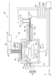
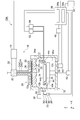
- FIGS. 1 and 2 are cross-sectional views schematically showing a plasma processing apparatus according to an embodiment.
- the head part 44 in FIG. 1 is accommodated.
- FIGS. 1 and 2 show an XYZ orthogonal coordinate system.
- the plasma processing apparatus 10 shown in FIGS. 1 and 2 is an atomic layer deposition apparatus (ALD apparatus).
- the plasma processing apparatus 10 includes a processing chamber 12, a gas supply source 36 that supplies a gas G into the processing chamber 12, and a plasma generator 16 that generates plasma P generated from the gas G in the processing chamber 12.
- the gas G contains a nitrogen atom and a hydrogen atom.
- the gas G includes, for example, ammonia gas.
- the gas G may include an inert gas such as Ar gas or nitrogen gas.
- the plasma processing apparatus 10 may include a substrate holder 14 that holds the substrate W in the processing chamber 12.
- the substrate W is a semiconductor substrate such as a silicon substrate, for example, and has a surface substantially parallel to the XY plane.
- the plasma P forms a nitride film such as a silicon nitride film on the substrate W, for example.
- the plasma generator 16 includes a microwave generator 18 for generating microwaves for plasma excitation, and a radial line slot antenna (Radial Line slot antenna for introducing the microwaves into the processing chamber 12. Slot Antenna; RLSA (registered trademark) 26.
- the microwave generator 18 is connected via a waveguide 20 to a mode converter 22 that converts a microwave mode.
- the mode converter 22 is connected to the radial line slot antenna 26 via a coaxial waveguide 24 having an inner waveguide 24a and an outer waveguide 24b.
- the frequency of the microwave generated by the microwave generator 18 is 2.45 GHz, for example.
- the radial line slot antenna 26 includes a dielectric window 34 that closes the opening 12 a formed in the processing chamber 12, a slot plate 32 provided outside the dielectric window 34, and a cooling jacket provided outside the slot plate 32. 30 and a dielectric plate 28 disposed between the slot plate 32 and the cooling jacket 30.
- the dielectric window 34 is disposed to face the substrate W.
- the dielectric window 34 is made of a ceramic material such as aluminum oxide (Al 2 O 3 ).
- An inner waveguide 24 a is connected to the center of the slot plate 32, and an outer waveguide 24 b is connected to the cooling jacket 30.
- the cooling jacket 30 also functions as a waveguide.
- the microwave propagates between the inner waveguide 24a and the outer waveguide 24b, propagates through the dielectric plate 28 between the slot plate 32 and the cooling jacket 30, and passes through the slot 32c to form the dielectric.
- the light passes through the window 34 and reaches the processing chamber 12.
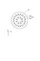
- FIG. 3 is a view of the slot plate 32 of the plasma processing apparatus 10 as viewed from the Z direction.
- FIG. 3 shows an XYZ orthogonal coordinate system.
- the slot plate 32 has a disk shape, for example.
- a plurality of concentric circles are formed, each of which includes a slot 32a extending in the first direction and a slot 32b extending in the second direction intersecting the first direction.
- the first direction is orthogonal to the second direction.
- the pair of slots 32 c are arranged at predetermined intervals in the radial direction from the center of the slot plate 32 and are arranged at predetermined intervals in the circumferential direction of the slot plate 32.
- the microwave transmitted through the dielectric window 34 passes through the pair of slots 32 c and is introduced into the processing chamber 12.
- the wavelength of the microwave is shortened when passing through the dielectric plate 28 (slow wave plate). For this reason, the microwave can be introduced into the processing chamber 12 more efficiently than the slot 32c.
- a gas supply port 12 b for plasma processing is formed on the side wall of the processing chamber 12.
- the gas supply port 12 b may be formed in the dielectric window 34, or may be formed in a gas supply unit that extends into the processing chamber 12.
- a gas supply source 36 is connected to the gas supply port 12b.
- plasma P is generated on the dielectric window 34 side in the processing chamber 12.
- the generated plasma P diffuses toward the substrate W.
- An exhaust port 12 c for exhausting the gas in the processing chamber 12 is formed at the bottom of the processing chamber 12.
- the exhaust port 12c has an APC (Auto Pressure Control)
- a vacuum pump 40 is connected via a valve 38.
- a temperature adjuster 42 for adjusting the temperature of the substrate holder 14 is connected to the substrate holder 14.
- the temperature of the substrate holder 14 is preferably, for example, 200 to 500 ° C., more preferably 300 to 400 ° C.
- the plasma processing apparatus 10 includes a head portion 44 in which a gas supply port 44a for supplying a source gas (precursor) for atomic layer deposition and a purge gas onto the substrate W is formed.
- the head portion 44 is connected to the driving device 48 by a support portion 46 that supports the head portion 44.
- the driving device 48 is disposed outside the processing chamber 12.
- the head unit 44 and the support unit 46 can be moved in the X direction by the driving device 48.
- the processing chamber 12 is provided with a storage portion 12 d for storing the head portion 44. As shown in FIG. 2, when the head unit 44 is stored in the storage unit 12d, the storage unit 12d is isolated by the movement of the shutter 50 in the Z direction.
- the plasma processing apparatus 10 shown in FIGS. 1 and 2 is the same except for whether or not the head portion 44 is housed in the housing portion 12d.
- the hollow support 46 is connected to and communicated with a source gas supply source 52 for atomic layer deposition and a purge gas supply source 54.
- the source gas and the purge gas are supplied from the head unit 44 onto the substrate W via the support unit 46 from the source gas supply source 52 and the purge gas supply source 54, respectively.
- the plasma processing apparatus 10 includes a photodetector 70 that detects light emission from the plasma P.
- the light detector 70 includes a condensing lens 62 disposed to face a window 60 provided on the side wall of the processing chamber 12. Light emitted from the plasma P passes through the window 60 and enters the condenser lens 62.
- a spectroscope 66 is connected to the condenser lens 62 via an optical fiber 64. The light split by the spectroscope 66 is introduced into a photomultiplier tube 68.
- the photodetector 70 is, for example, an emission spectroscopic analyzer (OES).
- OES emission spectroscopic analyzer
- the light detector 70 may be arranged at any position where light emission from the plasma P can be detected.
- the plasma processing apparatus 10 includes a control unit 56 that controls the entire apparatus.
- the control unit 56 includes a microwave generator 18, a vacuum pump 40, a temperature controller 42, a driving device 48, a gas supply source 36 for plasma processing, a source gas supply source 52 for atomic layer deposition, a purge gas supply source 54, an optical device Each is connected to a detector 70.
- the control unit 56 outputs the microwave output, the pressure in the processing chamber 12, the temperature of the substrate holder 14, the movement of the head unit 44 in the X direction, the gas for plasma processing, the source gas for purging the atomic layer, and the purge gas.
- the gas flow rate and the gas flow time can be controlled respectively.
- the control unit 56 is, for example, a computer, and includes an arithmetic device 56a such as a CPU and a storage device 56b such as a memory or a hard disk.
- the storage device 56b may be a computer-readable recording medium.
- the recording medium is, for example, a CD, NAND, BD, HDD, USB, or the like. Data from the photodetector 70 is recorded in the storage device 56b.
- a display device 58 that displays various data to be controlled may be connected to the control unit 56.
- control unit 56 determines the intensity ratio between the first peak caused by hydrogen atoms and the second peak caused by hydrogen atoms, which is different from the first peak, in the spectrum of the detected plasma emission intensity.
- the plasma P is evaluated using a result obtained by comparing the above with a reference value calculated in advance from the relationship between the intensity ratio and the index representing the film quality of the nitride film.
- the storage device 56b stores a program that causes a computer to execute the following plasma evaluation procedure.
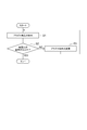
- FIG. 4 is a flowchart showing each step of the plasma evaluation method according to an embodiment.
- plasma P for forming a nitride film is evaluated by an atomic layer deposition method.
- the plasma evaluation method according to the present embodiment can be performed using the above-described plasma processing apparatus 10, and is performed as follows, for example, without the substrate W in FIG.
- the light emission from the plasma P generated from the gas G is detected by the photodetector 70 shown in FIG. 2 (step S1).
- Spectral spectrum data of the plasma emission intensity obtained by the photodetector 70 is recorded in the storage device 56b.
- step S1 the intensity ratio between the first peak caused by hydrogen atoms and the second peak caused by hydrogen atoms is different from the first peak in the spectrum of the detected plasma emission intensity by the control unit 56. Is calculated. On the other hand, from the relationship between the intensity ratio and an index representing the film quality of the nitride film (for example, the wet etching rate of the nitride film with respect to a 0.5% hydrofluoric acid aqueous solution) A corresponding reference value is calculated. Thereafter, the control unit 56 evaluates the plasma P using the result of comparing the intensity ratio with the reference value (step S2). In step S2, for example, it is determined whether or not the intensity ratio is greater than or equal to a reference value.
- the peak wavelength of the first peak is, for example, 656.2 nm
- the peak wavelength of the second peak is, for example, 486.1 nm.
- the intensity ratio is expressed by, for example, I 656 / I 486 .
- the intensity ratio I 656 / I 486 is greater than or equal to a reference value (for example, 4.5), it indicates that the plasma condition of the plasma P is a plasma condition that can form a nitride film with good film quality.
- the intensity ratio I 656 / I 486 is smaller than the reference value, it indicates that the plasma condition of the plasma P is not a plasma condition that can form a nitride film with good film quality. If the plasma conditions are not such that a good quality nitride film can be formed, an alarm or the like may be displayed on the display device 58. In this way, the plasma P can be evaluated. Such plasma evaluation is effective when a nitride film is formed using a photodetector incorporated in a plasma processing apparatus.
- the conditions of the plasma P may be changed so that the intensity ratio I 656 / I 486 is equal to or higher than the reference value (step S3).
- the plasma condition can be changed to a plasma condition capable of forming a nitride film having a good film quality.
- the conditions of the plasma P that can be changed include the microwave output supplied to the microwave generator 18, the pressure in the processing chamber 12, the temperature of the substrate holder 14, the gas type of the gas G, the gas flow rate, the flow rate ratio, and the gas. The flow time, the place where the gas G is supplied, etc. Of these, the microwave power supplied to the microwave generator 18 and the pressure in the processing chamber 12 have a great influence on the state of the plasma P.
- step S3 the process may return to step S1.
- feedback control can be performed so as to maintain the plasma conditions capable of forming a nitride film of good film quality.
- the plasma evaluation method of the present embodiment it is possible to evaluate whether or not the plasma P capable of forming a nitride film with good film quality is generated from the intensity ratio of two peaks caused by hydrogen atoms. For this reason, it is not necessary to form a nitride film or to evaluate the nitride film for each plasma condition. Therefore, plasma conditions that can form a dense nitride film having good film quality can be determined in a short time (for example, within 10 minutes). As a result, the throughput of the nitride film formation process is improved.
- the plasma evaluation method of the present embodiment it is possible to monitor the change with time of the state of the plasma P. Thereby, the timing which replaces the component of the plasma processing apparatus 10 is known.
- This plasma evaluation method is effective in determining the replacement timing of the dielectric window 34 that is particularly easily deteriorated among the components of the plasma processing apparatus 10.
- the plasma evaluation method according to the present embodiment may be performed in the state where the substrate W is present in FIG.
- the state of the plasma P can be monitored in real time while forming a nitride film on the substrate W by atomic layer deposition. Therefore, it is possible to stably form a nitride film having a good film quality.
- the electron temperature of the plasma P is as low as 1.5 eV or less, so that when the nitride film is formed, the processing speed of the plasma nitriding treatment is improved while reducing damage. be able to.
- the radial line slot antenna 26 the microwave can be uniformly introduced into the processing chamber 12, and as a result, a uniform plasma P can be generated in a wide range.
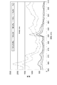
- FIG. 5 is a graph showing an example of a spectrum of plasma emission intensity.
- the vertical axis represents the emission intensity.
- the horizontal axis indicates the wavelength (nm).
- FIG. 5 shows a spectral spectrum at 200 to 800 nm when the following gases 1 to 6 are used as the gas G for generating the plasma P, respectively.
- Gas 1 Mixed gas of NH 3 , Ar, and N 2 2
- Mixed gas of NH 3 and Ar 3 Mixed gas of NH 3 and N 2 4: NH 3
- Gas 5 Mixed gas of N 2 and Ar 6: N 2
- the silicon-containing compound adsorbed on the substrate W was plasma-nitrided by setting the pressure in the processing chamber 12 during the plasma processing to 5 Torr (666.5 Pa).
- a silicon nitride film is formed (a silicon-containing compound is easily subjected to plasma nitriding treatment), and in the gases 5 and 6 not containing NH 3 , it is difficult to form a silicon nitride film. (Silicon-containing compounds are difficult to be plasma-nitrided).
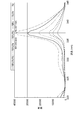
- 6 to 8 are graphs showing an enlarged part of the spectrum shown in FIG.
- the spectrum at 460 to 510 nm is shown.
- a spectrum at 600 to 800 nm is shown.
- the spectrum at 320 to 345 nm is shown.
- a peak due to a hydrogen atom having a peak wavelength of 486.1 nm is detected in gases 1 to 4.
- gases 1 to 4 peaks caused by hydrogen atoms having a peak wavelength of 656.2 nm are detected. These peaks are attributed to hydrogen atoms generated by dissociation of NH 3 .
- a peak due to N 2 having a peak wavelength of 337.1 nm is detected, but a peak due to NH having a peak wavelength of 336.0 nm is not detected. Since no peak due to NH is detected, it is assumed that NH 3 is dissociated into H and NH 2 radicals.
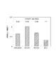
- FIG. 9 is a graph showing an example of the relationship between the intensity ratio of two peaks caused by hydrogen atoms and the wet etching rate of the silicon nitride film with respect to a 0.5% hydrofluoric acid aqueous solution.
- the vertical axis represents the intensity ratio ([peak intensity at a peak wavelength of 656.2 nm caused by hydrogen atoms) / [peak intensity at a peak wavelength of 486.1 nm caused by hydrogen atoms]).
- the horizontal axis indicates the type of gas G for generating plasma P.
- FIG. 9 shows the wet etching rate when the formed silicon nitride film is wet etched with a 0.5% hydrofluoric acid aqueous solution.
- This value is a relative value when the wet etching rate of the thermal oxide film obtained by thermally oxidizing silicon at 950 ° C. using WVG (Wet Vapor Generator) is 1.
- WVG Weight Vapor Generator
- the value of the wet etching rate is 1 or less.
- the wet etching rate of the silicon nitride film is 0.53, and the intensity ratio is 4.65.
- the wet etching rate of the silicon nitride film is 0.48, and the intensity ratio is 5.02.
- gas 3 the wet etching rate of the silicon nitride film is 0.49 and the intensity ratio is 4.70.
- the wet etching rate of the silicon nitride film is 1.1, and the intensity ratio is 4.33. From the graph of FIG. 9, it can be seen that as the intensity ratio increases, the wet etching rate of the silicon nitride film decreases (the film quality of the silicon nitride film improves and becomes dense). That is, as the intensity ratio increases, the wet etching rate of the silicon nitride film monotonously decreases. It is considered that the larger the intensity ratio, the more NH 2 radicals are generated. It is considered that the film quality of the silicon nitride film is improved by the progress of the nitriding process by the NH 2 radical.
- the flow rate ratio of NH 3 gas to plasma gas (Ar + N 2 ) is 0.15 for gas 1, 0.5 for gas 2, 0.5 for gas 3, and 1 for gas 4.
- a preferable flow rate ratio is less than 1, more preferably 0.8 or less, and 0.5 or less and 0.05 or more are good.
- the silicon nitride film formed by the atomic layer deposition method includes more Si—NH group bonds than the silicon nitride film formed by the low pressure chemical vapor deposition (LPCVD) method.
- LPCVD low pressure chemical vapor deposition
- the SIMS analysis results also show that the hydrogen atom content in the silicon nitride film formed by atomic layer deposition is higher than the hydrogen atom content in the silicon nitride film formed by LPCVD. .
- the wet etching rate of the silicon nitride film formed by the LPCVD method is smaller than the wet etching rate of the silicon nitride film formed by the atomic layer deposition method. Therefore, it can be seen that as the hydrogen atom content in the silicon nitride film increases, the wet etching rate of the silicon nitride film increases (the film quality of the silicon nitride film decreases).
- FIG. 10 is a graph showing an example of the relationship between the intensity of one peak caused by hydrogen atoms and the wet etching rate of the silicon nitride film with respect to a 0.5% hydrofluoric acid aqueous solution.
- the vertical axis represents the peak intensity at a peak wavelength of 656.2 nm due to hydrogen atoms.
- the horizontal axis indicates the type of gas G for plasma generation.
- the peak intensity hardly changes between the gas 4 at which the wet etching rate of the silicon nitride film is 1.1 and the gas 3 at which the wet etching rate of the silicon nitride film is 0.49.
- the peak intensity of gas 1 at which the wet etching rate of the silicon nitride film is 0.53 is larger than the peak intensity of gas 3 at which the wet etching rate of the silicon nitride film is 0.49. That is, there is no correlation between the intensity ratio and the silicon nitride film wet etching rate as shown in FIG. 9 between the peak intensity and the silicon nitride film wet etching rate. Therefore, it is considered difficult to predict the film quality of the silicon nitride film only from the peak intensity at the peak wavelength of 656.2 nm caused by hydrogen atoms.
- FIG. 11 is a cross-sectional view schematically showing a plasma processing apparatus according to an embodiment.
- a plasma processing apparatus 10A shown in FIG. 11 has the same configuration as the plasma processing apparatus 10 except for the following points.
- the plasma processing apparatus 10 ⁇ / b> A includes a donut-shaped head portion 44 b instead of the head portion 44.
- the head part 44b is supported by the support part 46a.
- the head portion 44b may be rotated on the XY plane.
- the head portion 44b has a ring portion 44r in which a gas supply port for supplying a source gas (precursor) for atomic layer deposition and a purge gas onto the substrate W is formed toward the center of the substrate W.
- the ring portion 44r is made of, for example, quartz.
- the source gas includes, for example, a silicon-containing compound.
- the purge gas includes an inert gas such as Ar gas or nitrogen gas.
- the ring portion 44r is disposed along the outer periphery of the substrate W.
- a source gas supply source 52 for atomic layer deposition and a purge gas supply source 54 are connected to and communicated with the ring portion 44r. The source gas and the purge gas are supplied from the source gas supply source 52 and the purge gas supply source 54 to the head portion 44b, respectively, and are supplied on the substrate W from the ring portion 44r inward.
- a recess 34 a is formed on the lower surface of the dielectric window 34.
- the microwave efficiently passes through the dielectric window 34 and is introduced into the chamber 12.
- a gas supply port 12d for plasma processing is formed in the dielectric window 34.
- the gas supply port 12d passes through the center of the dielectric window 34 and the slot plate 32 and communicates with the inner waveguide 24a.
- the gas G supplied from the gas supply source 36 may be supplied into the processing chamber 12 from the gas supply port 12d via the inner waveguide 24a. Nitrogen gas such as NH 3 gas, N 2 gas, Ar gas, plasma generation gas, and purge gas are supplied from the gas supply port 12d.
- a plurality of plasma processing gas supply ports 12 b are formed along the annular region of the side wall of the processing chamber 12.
- the gas supply ports 12b are radially formed uniformly from the outside to the center of the processing chamber 12 so as to communicate with a ring-shaped gap formed inside the side wall of the processing chamber 12.
- plasma generating gas and purge gas such as N 2 gas and Ar gas are supplied from the gas supply port 12b.
- a nitriding gas such as NH 3 gas may be supplied.
- the plasma processing apparatus 10A includes an edge ring 12e in which a gas supply port for plasma processing is formed in an annular ring member.
- the gas supply ports 12 b are uniformly formed toward the substrate W and toward the center in the chamber 12.
- the edge ring 12e is made of quartz, for example.
- the gas G supplied from the gas supply source 36 may be supplied into the processing chamber 12 from the edge ring 12e. Nitrogen gas such as NH 3 gas, N 2 gas, Ar gas, plasma generation gas, and purge gas are supplied from the gas supply port 12e.
- the gas type, gas flow rate, flow rate ratio, gas flow time, and the like of the gas G supplied from the gas supply ports 12b and 12d and the edge ring 12e can be controlled independently.
- FIG. 12 is a timing chart schematically showing a plasma processing method according to an embodiment.
- the plasma processing method according to the present embodiment includes a step of performing plasma processing on the layer adsorbed on the substrate W using the plasma P evaluated by the plasma evaluation method. Thereby, a nitride film having a good film quality is formed on the substrate W.
- the plasma processing method is performed by repeating the following steps 1 to 4 using, for example, the plasma processing apparatus 10A. Thereby, a nitride film having a thickness of 1 to 15 nm, for example, is formed.
- a source gas such as dichlorosilane is adsorbed on the substrate W to generate a silicon-containing compound (time t 1 to t 2 ).
- the source gas includes Ar (flow rate from the gas supply port 12b: 900 sccm), N 2 (flow rate from the gas supply port 12b: 900 sccm), and dichlorosilane (flow rate from the ring portion 44r: 280 sccm).
- Step 2 After evacuating the processing chamber 12 as necessary (time t 2 to t 3 ), the excessively adsorbed source gas is removed with a purge gas (time t 3 to t 4 ).
- the purge gas is Ar (flow rate from the gas supply port 12b: 900 sccm, flow rate from the gas supply port 12d and the edge ring 12e: 500 sccm, flow rate from the ring portion 44r: 500 sccm), N 2 (from the gas supply port 12b). And a flow rate from the gas supply port 12d and the edge ring 12e: 400 sccm).
- Step 3 Plasma nitridation treatment is performed on the layer made of the source gas (silicon-containing compound) adsorbed on the substrate W using the plasma P generated from the gas G such as ammonia (time t 4 to t 5 ). .
- the plasma P is generated by turning on the microwave power (for example, 4000 W).
- Step 4 After evacuating the processing chamber 12 as necessary (time t 5 to t 6 ), the gas remaining in the processing chamber 12 is removed with a purge gas (time t 6 to t 7 ).
- the purge gas in step 4 may be the same as the purge gas in step 2.
- a silicon nitride film having a desired film thickness (for example, 1 to 15 nm) is formed by performing steps 1 to 4 as described above as one cycle.
- the substrate W may be preliminarily plasma-nitrided using the plasma P generated from the gas G containing nitrogen atoms and hydrogen atoms.
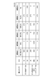
- FIG. 13 is a chart showing an example of the gas flow rate when forming the silicon nitride film.
- FIG. 13 shows the flow rate of each gas included in the gas G supplied from the gas supply ports 12b and 12d and the edge ring 12e in Step 3 to be described later for Experimental Examples 1 to 6.
- the pressure in the processing chamber 12 during plasma processing is 5 Torr and the temperature is 400 ° C.
- the Ar flow rate from the ring portion 44r is, for example, 100 sccm.
- Experimental Examples 1 to 4 correspond to the gas flow rates when forming the silicon nitride film in the experimental examples of FIGS.
Landscapes
- Chemical & Material Sciences (AREA)
- Engineering & Computer Science (AREA)
- Physics & Mathematics (AREA)
- Mechanical Engineering (AREA)
- Organic Chemistry (AREA)
- General Chemical & Material Sciences (AREA)
- Chemical Kinetics & Catalysis (AREA)
- Materials Engineering (AREA)
- Metallurgy (AREA)
- Plasma & Fusion (AREA)
- Spectroscopy & Molecular Physics (AREA)
- Electromagnetism (AREA)
- Analytical Chemistry (AREA)
- Inorganic Chemistry (AREA)
- General Physics & Mathematics (AREA)
- Chemical Vapour Deposition (AREA)
- Formation Of Insulating Films (AREA)
Abstract
Description
(1)処理チャンバ内において成膜材料を基板上に吸着させる。
(2)余分に吸着した成膜材料をパージガスにより除去する。
(3)窒素原子を含むガスから生成されるプラズマを用いて成膜材料をプラズマ窒化処理する。
(4)処理チャンバ内に残存するガスをパージガスにより除去する。
Slot Antenna;RLSA:登録商標)26とを備える。マイクロ波発生器18は、導波管20を介して、マイクロ波のモードを変換するモード変換器22に接続されている。モード変換器22は、内側導波管24a及び外側導波管24bを有する同軸導波管24を介してラジアルラインスロットアンテナ26に接続されている。これにより、マイクロ波発生器18によって発生したマイクロ波は、モード変換器22においてモード変換され、ラジアルラインスロットアンテナ26に到達する。マイクロ波発生器18が発生するマイクロ波の周波数は、例えば2.45GHzである。
Control)バルブ38を介して真空ポンプ40が接続されている。基板ホルダ14には、基板ホルダ14の温度を調節するための温度調節器42が接続されている。基板ホルダ14の温度は、例えば200~500℃が好ましく、より好ましくは300~400℃に調節される。
まず、図2に示される光検出器70によって、ガスGから生成されるプラズマPからの発光を検出する(工程S1)。光検出器70によって得られたプラズマ発光強度の分光スペクトルデータは、記憶装置56bに記録される。
工程S1の後、制御部56によって、検出されたプラズマ発光強度の分光スペクトルにおいて水素原子に起因する第1のピークと第1のピークとは異なり水素原子に起因する第2のピークとの強度比を算出する。一方、当該強度比と窒化膜の膜質を表す指標(例えば0.5%フッ酸水溶液に対する窒化膜のウェットエッチングレート)との関係から、予め窒化膜の膜質が良好であるか否かの閾値に対応する基準値を算出しておく。その後、制御部56によって、強度比を基準値と比較した結果を用いてプラズマPの評価を行う(工程S2)。工程S2では、例えば強度比が基準値以上か否かを判断する。
工程S2の後、強度比I656/I486が基準値よりも小さい場合、強度比I656/I486が基準値以上となるようにプラズマPの条件を変更してもよい(工程S3)。これにより、プラズマ条件を、良好な膜質の窒化膜を形成可能なプラズマ条件に変更することができる。変更可能なプラズマPの条件としては、マイクロ波発生器18に供給されるマイクロ波出力、処理チャンバ12内の圧力、基板ホルダ14の温度、ガスGのガス種、ガス流量、流量比及びガスを流す時間、ガスGを供給する場所等が挙げられる。これらの中でプラズマPの状態に及ぼす影響が大きいのは、マイクロ波発生器18に供給されるマイクロ波出力、処理チャンバ12内の圧力である。
ガス1:NH3、Ar及びN2の混合ガス
ガス2:NH3及びArの混合ガス
ガス3:NH3及びN2の混合ガス
ガス4:NH3
ガス5:N2及びArの混合ガス
ガス6:N2
つまり、NH3を効率良く解離させて水素原子を生成させるためには、NH3にN2やArを混合することが有効である。この場合、プラズマ中でN2およびArが励起する際に高速電子が生成されるので、この電子がNH3を解離し易くし、効率良く水素原子が生成されると考えられる。
この場合、プラズマガス(Ar+N2)に対するNH3ガスの流量比は、ガス1では0.15、ガス2では0.5、ガス3では0.5、ガス4では1である。好ましい流量比は1未満であり、より好ましくは、0.8以下であり、0.5以下0.05以上が良い。
(ステップ1)処理チャンバ12内において、例えばジクロロシラン等の原料ガスを基板W上に吸着させてシリコン含有化合物を生成する(時刻t1~t2)。一例において、原料ガスは、Ar(ガス供給口12bからの流量:900sccm)、N2(ガス供給口12bからの流量:900sccm)及びジクロロシラン(リング部44rからの流量:280sccm)を含む。
(ステップ2)必要に応じて処理チャンバ12内を真空引き(時刻t2~t3)した後、余分に吸着した原料ガスをパージガスにより除去する(時刻t3~t4)。一例において、パージガスは、Ar(ガス供給口12bからの流量:900sccm、ガス供給口12d及びエッジリング12eからの流量:500sccm、リング部44rからの流量:500sccm)、N2(ガス供給口12bからの流量:900sccm)及びアンモニア(ガス供給口12d及びエッジリング12eからの流量:400sccm)を含む。
(ステップ3)例えばアンモニア等のガスGから生成されるプラズマPを用いて、基板W上に吸着された原料ガス(シリコン含有化合物)からなる層をプラズマ窒化処理する(時刻t4~t5)。プラズマPは、マイクロ波のパワー(例えば4000W)をONにすることにより生成される。
(ステップ4)必要に応じて処理チャンバ12内を真空引き(時刻t5~t6)した後、処理チャンバ12内に残存するガスをパージガスにより除去する(時刻t6~t7)。ステップ4のパージガスはステップ2のパージガスと同じであってもよい。
以上のようなステップ1~4を1サイクルとして、所望の膜厚(例えば1~15nm)のシリコン窒化膜が形成される。
Claims (8)
- 原子層堆積法により窒化膜を形成するためのプラズマを評価するプラズマ評価方法であって、
窒素原子及び水素原子を含むガスから生成される前記プラズマからの発光を検出する工程と、
検出された前記発光の強度の分光スペクトルにおいて水素原子に起因する第1のピークと前記第1のピークとは異なり水素原子に起因する第2のピークとの強度比を、予め前記強度比と前記窒化膜の膜質を表す指標との関係から算出された基準値と比較した結果を用いて、前記プラズマの評価を行う工程と、
を含む、プラズマ評価方法。 - 前記第1のピークのピーク波長が656.2nmであり、前記第2のピークのピーク波長が486.1nmである、請求項1に記載のプラズマ評価方法。
- 前記プラズマの評価を行う工程の後、前記強度比が前記基準値よりも小さい場合に、前記強度比が前記基準値以上となるように前記プラズマの条件を変更する工程を更に含む、請求項1又は2に記載のプラズマ評価方法。
- 前記プラズマの条件を変更する工程の後、前記プラズマからの発光を検出する工程に戻る、請求項3に記載のプラズマ評価方法。
- 前記プラズマが、マイクロ波によって生成される、請求項1~4のいずれか一項に記載のプラズマ評価方法。
- 前記プラズマが、ラジアルラインスロットアンテナによって生成される、請求項5に記載のプラズマ評価方法。
- 請求項1~6のいずれか一項に記載のプラズマ評価方法によって評価された前記プラズマを用いて、基板上に吸着された層に対してプラズマ処理を施す工程を含む、プラズマ処理方法。
- 原子層堆積法により窒化膜を形成するためのプラズマ処理装置であって、
処理チャンバと、
前記処理チャンバ内に、窒素原子及び水素原子を含むガスを供給するガス供給源と、
前記処理チャンバ内に、前記ガスから生成されるプラズマを発生させるプラズマ発生器と、
前記プラズマからの発光を検出する光検出器と、
検出された前記発光の強度の分光スペクトルにおいて水素原子に起因する第1のピークと前記第1のピークとは異なり水素原子に起因する第2のピークとの強度比を、予め前記強度比と前記窒化膜の膜質を表す指標との関係から算出された基準値と比較した結果を用いて、前記プラズマの評価を行う制御部と、
を備える、プラズマ処理装置。
Priority Applications (3)
| Application Number | Priority Date | Filing Date | Title |
|---|---|---|---|
| JP2013511021A JP5663658B2 (ja) | 2011-04-18 | 2012-04-18 | プラズマ評価方法、プラズマ処理方法及びプラズマ処理装置 |
| US14/112,172 US20140227458A1 (en) | 2011-04-18 | 2012-04-18 | Plasma evaluation method, plasma processing method and plasma processing apparatus |
| KR1020137027285A KR101860592B1 (ko) | 2011-04-18 | 2012-04-18 | 플라즈마 평가 방법, 플라즈마 처리 방법 및 플라즈마 처리 장치 |
Applications Claiming Priority (2)
| Application Number | Priority Date | Filing Date | Title |
|---|---|---|---|
| JP2011-092280 | 2011-04-18 | ||
| JP2011092280 | 2011-04-18 |
Publications (1)
| Publication Number | Publication Date |
|---|---|
| WO2012144523A1 true WO2012144523A1 (ja) | 2012-10-26 |
Family
ID=47041629
Family Applications (1)
| Application Number | Title | Priority Date | Filing Date |
|---|---|---|---|
| PCT/JP2012/060474 Ceased WO2012144523A1 (ja) | 2011-04-18 | 2012-04-18 | プラズマ評価方法、プラズマ処理方法及びプラズマ処理装置 |
Country Status (5)
| Country | Link |
|---|---|
| US (1) | US20140227458A1 (ja) |
| JP (1) | JP5663658B2 (ja) |
| KR (1) | KR101860592B1 (ja) |
| TW (1) | TW201306082A (ja) |
| WO (1) | WO2012144523A1 (ja) |
Cited By (14)
| Publication number | Priority date | Publication date | Assignee | Title |
|---|---|---|---|---|
| CN103866285A (zh) * | 2012-12-18 | 2014-06-18 | 中国科学院微电子研究所 | 利用原子层沉积制备薄膜的方法 |
| CN104046955A (zh) * | 2013-03-14 | 2014-09-17 | Asmip控股有限公司 | 用于在低温下沉积SiN的Si前体 |
| US20140273477A1 (en) * | 2013-03-14 | 2014-09-18 | Asm Ip Holding B.V. | Si PRECURSORS FOR DEPOSITION OF SiN AT LOW TEMPERATURES |
| JP2015165564A (ja) * | 2014-02-28 | 2015-09-17 | ウォニク アイピーエス カンパニー リミテッド | 窒化膜の製造方法及び窒化膜の圧縮応力の制御方法 |
| JP5840268B1 (ja) * | 2014-08-25 | 2016-01-06 | 株式会社日立国際電気 | 基板処理装置、半導体装置の製造方法および記録媒体 |
| US9362109B2 (en) | 2013-10-16 | 2016-06-07 | Asm Ip Holding B.V. | Deposition of boron and carbon containing materials |
| US9401273B2 (en) | 2013-12-11 | 2016-07-26 | Asm Ip Holding B.V. | Atomic layer deposition of silicon carbon nitride based materials |
| US9576790B2 (en) | 2013-10-16 | 2017-02-21 | Asm Ip Holding B.V. | Deposition of boron and carbon containing materials |
| US9576792B2 (en) | 2014-09-17 | 2017-02-21 | Asm Ip Holding B.V. | Deposition of SiN |
| US10410857B2 (en) | 2015-08-24 | 2019-09-10 | Asm Ip Holding B.V. | Formation of SiN thin films |
| US10580645B2 (en) | 2018-04-30 | 2020-03-03 | Asm Ip Holding B.V. | Plasma enhanced atomic layer deposition (PEALD) of SiN using silicon-hydrohalide precursors |
| US11056353B2 (en) | 2017-06-01 | 2021-07-06 | Asm Ip Holding B.V. | Method and structure for wet etch utilizing etch protection layer comprising boron and carbon |
| CN114791416A (zh) * | 2021-01-26 | 2022-07-26 | 富兰登科技股份有限公司 | 以光谱量测物质的物理状态的装置及其方法 |
| US11996286B2 (en) | 2020-12-09 | 2024-05-28 | Asm Ip Holding B.V. | Silicon precursors for silicon nitride deposition |
Families Citing this family (9)
| Publication number | Priority date | Publication date | Assignee | Title |
|---|---|---|---|---|
| JP6165982B2 (ja) * | 2013-11-01 | 2017-07-19 | 東京エレクトロン株式会社 | プラズマ処理における空間分解発光分光分析 |
| KR102186070B1 (ko) * | 2014-09-17 | 2020-12-07 | 세메스 주식회사 | 기판 처리 장치 및 플라즈마 처리 방법 |
| JP6823555B2 (ja) * | 2017-07-05 | 2021-02-03 | アークレイ株式会社 | プラズマ分光分析方法 |
| KR102516885B1 (ko) * | 2018-05-10 | 2023-03-30 | 삼성전자주식회사 | 증착 장비 및 이를 이용한 반도체 장치 제조 방법 |
| JP2020056104A (ja) | 2018-10-02 | 2020-04-09 | エーエスエム アイピー ホールディング ビー.ブイ. | 選択的パッシベーションおよび選択的堆積 |
| US12482648B2 (en) | 2018-10-02 | 2025-11-25 | Asm Ip Holding B.V. | Selective passivation and selective deposition |
| US10761029B1 (en) * | 2019-09-05 | 2020-09-01 | Schenck Process Llc | Laser-induced spectroscopy system and process |
| KR102860972B1 (ko) | 2020-06-10 | 2025-09-16 | 삼성전자주식회사 | 반도체 증착 모니터링 장치 |
| KR102686910B1 (ko) * | 2021-08-09 | 2024-07-19 | 삼성전자주식회사 | 반도체 소자의 제조 장치 및 반도체 소자의 제조 방법 |
Citations (3)
| Publication number | Priority date | Publication date | Assignee | Title |
|---|---|---|---|---|
| JP2001284322A (ja) * | 2000-03-30 | 2001-10-12 | Sharp Corp | プラズマプロセス装置、プラズマプロセス装置の制御方法および不良品判定方法 |
| JP2006045640A (ja) * | 2004-08-06 | 2006-02-16 | Tokyo Electron Ltd | 薄膜形成方法及び薄膜形成装置 |
| JP2010186885A (ja) * | 2009-02-12 | 2010-08-26 | Mitsui Eng & Shipbuild Co Ltd | 原子層成長装置および薄膜形成方法 |
Family Cites Families (10)
| Publication number | Priority date | Publication date | Assignee | Title |
|---|---|---|---|---|
| JPS63289924A (ja) * | 1987-05-22 | 1988-11-28 | Canon Inc | 機能性堆積膜形成方法 |
| JPH02148715A (ja) * | 1988-11-29 | 1990-06-07 | Canon Inc | 半導体デバイスの連続形成装置 |
| JP2875945B2 (ja) * | 1993-01-28 | 1999-03-31 | アプライド マテリアルズ インコーポレイテッド | Cvdにより大面積のガラス基板上に高堆積速度でシリコン窒化薄膜を堆積する方法 |
| JPH09306869A (ja) * | 1996-05-17 | 1997-11-28 | Sony Corp | プラズマcvd方法およびこれにより形成された金属膜を有する半導体装置 |
| US6391803B1 (en) * | 2001-06-20 | 2002-05-21 | Samsung Electronics Co., Ltd. | Method of forming silicon containing thin films by atomic layer deposition utilizing trisdimethylaminosilane |
| US7022605B2 (en) * | 2002-11-12 | 2006-04-04 | Micron Technology, Inc. | Atomic layer deposition methods |
| US7749564B2 (en) * | 2005-03-31 | 2010-07-06 | Caterpillar Inc. | Method and apparatus for the production of thin film coatings |
| US7742167B2 (en) * | 2005-06-17 | 2010-06-22 | Perkinelmer Health Sciences, Inc. | Optical emission device with boost device |
| JP4891667B2 (ja) * | 2005-08-22 | 2012-03-07 | 株式会社東芝 | 半導体装置の製造方法 |
| US7651961B2 (en) * | 2007-03-30 | 2010-01-26 | Tokyo Electron Limited | Method for forming strained silicon nitride films and a device containing such films |
-
2012
- 2012-04-17 TW TW101113584A patent/TW201306082A/zh unknown
- 2012-04-18 WO PCT/JP2012/060474 patent/WO2012144523A1/ja not_active Ceased
- 2012-04-18 JP JP2013511021A patent/JP5663658B2/ja not_active Expired - Fee Related
- 2012-04-18 KR KR1020137027285A patent/KR101860592B1/ko not_active Expired - Fee Related
- 2012-04-18 US US14/112,172 patent/US20140227458A1/en not_active Abandoned
Patent Citations (3)
| Publication number | Priority date | Publication date | Assignee | Title |
|---|---|---|---|---|
| JP2001284322A (ja) * | 2000-03-30 | 2001-10-12 | Sharp Corp | プラズマプロセス装置、プラズマプロセス装置の制御方法および不良品判定方法 |
| JP2006045640A (ja) * | 2004-08-06 | 2006-02-16 | Tokyo Electron Ltd | 薄膜形成方法及び薄膜形成装置 |
| JP2010186885A (ja) * | 2009-02-12 | 2010-08-26 | Mitsui Eng & Shipbuild Co Ltd | 原子層成長装置および薄膜形成方法 |
Cited By (41)
| Publication number | Priority date | Publication date | Assignee | Title |
|---|---|---|---|---|
| CN103866285A (zh) * | 2012-12-18 | 2014-06-18 | 中国科学院微电子研究所 | 利用原子层沉积制备薄膜的方法 |
| US11587783B2 (en) | 2013-03-14 | 2023-02-21 | Asm Ip Holding B.V. | Si precursors for deposition of SiN at low temperatures |
| US11069522B2 (en) | 2013-03-14 | 2021-07-20 | Asm Ip Holding B.V. | Si precursors for deposition of SiN at low temperatures |
| US20140273528A1 (en) * | 2013-03-14 | 2014-09-18 | Asm Ip Holding B.V. | Si PRECURSORS FOR DEPOSITION OF SiN AT LOW TEMPERATURES |
| JP7663657B2 (ja) | 2013-03-14 | 2025-04-16 | エーエスエム・アイピー・ホールディング・ベー・フェー | 低温でのSiNの堆積用Si前駆体 |
| JP2024023223A (ja) * | 2013-03-14 | 2024-02-21 | エーエスエム・アイピー・ホールディング・ベー・フェー | 低温でのSiNの堆積用Si前駆体 |
| CN104046955B (zh) * | 2013-03-14 | 2018-12-07 | Asm Ip 控股有限公司 | 用于在低温下沉积SiN的Si前体 |
| US11289327B2 (en) | 2013-03-14 | 2022-03-29 | Asm Ip Holding B.V. | Si precursors for deposition of SiN at low temperatures |
| US20140273477A1 (en) * | 2013-03-14 | 2014-09-18 | Asm Ip Holding B.V. | Si PRECURSORS FOR DEPOSITION OF SiN AT LOW TEMPERATURES |
| US9564309B2 (en) * | 2013-03-14 | 2017-02-07 | Asm Ip Holding B.V. | Si precursors for deposition of SiN at low temperatures |
| US10424477B2 (en) | 2013-03-14 | 2019-09-24 | Asm Ip Holding B.V. | Si precursors for deposition of SiN at low temperatures |
| CN104046955A (zh) * | 2013-03-14 | 2014-09-17 | Asmip控股有限公司 | 用于在低温下沉积SiN的Si前体 |
| US9824881B2 (en) * | 2013-03-14 | 2017-11-21 | Asm Ip Holding B.V. | Si precursors for deposition of SiN at low temperatures |
| US10395917B2 (en) | 2013-03-14 | 2019-08-27 | Asm Ip Holding B.V. | Si precursors for deposition of SiN at low temperatures |
| US9905416B2 (en) | 2013-03-14 | 2018-02-27 | Asm Ip Holding B.V. | Si precursors for deposition of SiN at low temperatures |
| US10410856B2 (en) | 2013-10-16 | 2019-09-10 | Asm Ip Holding B.V. | Deposition of boron and carbon containing materials |
| US10790137B2 (en) | 2013-10-16 | 2020-09-29 | Asm Ip Holding B.V. | Deposition of boron and carbon containing materials |
| US9543140B2 (en) | 2013-10-16 | 2017-01-10 | Asm Ip Holding B.V. | Deposition of boron and carbon containing materials |
| US9922817B2 (en) | 2013-10-16 | 2018-03-20 | Asm Ip Holding B.V. | Deposition of boron and carbon containing materials |
| US9576790B2 (en) | 2013-10-16 | 2017-02-21 | Asm Ip Holding B.V. | Deposition of boron and carbon containing materials |
| US9362109B2 (en) | 2013-10-16 | 2016-06-07 | Asm Ip Holding B.V. | Deposition of boron and carbon containing materials |
| US10199211B2 (en) | 2013-12-11 | 2019-02-05 | Asm Ip Holding B.V. | Atomic layer deposition of silicon carbon nitride based materials |
| US9401273B2 (en) | 2013-12-11 | 2016-07-26 | Asm Ip Holding B.V. | Atomic layer deposition of silicon carbon nitride based materials |
| US9837263B2 (en) | 2013-12-11 | 2017-12-05 | Asm Ip Holding B.V. | Atomic layer deposition of silicon carbon nitride based materials |
| US10515794B2 (en) | 2013-12-11 | 2019-12-24 | Asm Ip Holding B.V. | Atomic layer deposition of silicon carbon nitride based materials |
| US10818489B2 (en) | 2013-12-11 | 2020-10-27 | Asm Ip Holding B.V. | Atomic layer deposition of silicon carbon nitride based material |
| JP2015165564A (ja) * | 2014-02-28 | 2015-09-17 | ウォニク アイピーエス カンパニー リミテッド | 窒化膜の製造方法及び窒化膜の圧縮応力の制御方法 |
| JP5840268B1 (ja) * | 2014-08-25 | 2016-01-06 | 株式会社日立国際電気 | 基板処理装置、半導体装置の製造方法および記録媒体 |
| US10741386B2 (en) | 2014-09-17 | 2020-08-11 | Asm Ip Holding B.V. | Deposition of SiN |
| US9576792B2 (en) | 2014-09-17 | 2017-02-21 | Asm Ip Holding B.V. | Deposition of SiN |
| US10262854B2 (en) | 2014-09-17 | 2019-04-16 | Asm Ip Holding B.V. | Deposition of SiN |
| US11367613B2 (en) | 2014-09-17 | 2022-06-21 | Asm Ip Holding B.V. | Deposition of SiN |
| US10410857B2 (en) | 2015-08-24 | 2019-09-10 | Asm Ip Holding B.V. | Formation of SiN thin films |
| US11133181B2 (en) | 2015-08-24 | 2021-09-28 | Asm Ip Holding B.V. | Formation of SiN thin films |
| US11784043B2 (en) | 2015-08-24 | 2023-10-10 | ASM IP Holding, B.V. | Formation of SiN thin films |
| US11056353B2 (en) | 2017-06-01 | 2021-07-06 | Asm Ip Holding B.V. | Method and structure for wet etch utilizing etch protection layer comprising boron and carbon |
| US10580645B2 (en) | 2018-04-30 | 2020-03-03 | Asm Ip Holding B.V. | Plasma enhanced atomic layer deposition (PEALD) of SiN using silicon-hydrohalide precursors |
| US11996286B2 (en) | 2020-12-09 | 2024-05-28 | Asm Ip Holding B.V. | Silicon precursors for silicon nitride deposition |
| JP2022114415A (ja) * | 2021-01-26 | 2022-08-05 | 富蘭登科技股▲ふん▼有限公司 | スペクトルにより物質の物理的状態を測定する装置及びスペクトルにより物質の物理的状態を測定する方法 |
| CN114791416A (zh) * | 2021-01-26 | 2022-07-26 | 富兰登科技股份有限公司 | 以光谱量测物质的物理状态的装置及其方法 |
| JP2024028965A (ja) * | 2021-01-26 | 2024-03-05 | 富蘭登科技股▲ふん▼有限公司 | スペクトルにより物質の物理的状態を測定する装置及びスペクトルにより物質の物理的状態を測定する方法 |
Also Published As
| Publication number | Publication date |
|---|---|
| JP5663658B2 (ja) | 2015-02-04 |
| JPWO2012144523A1 (ja) | 2014-07-28 |
| TW201306082A (zh) | 2013-02-01 |
| US20140227458A1 (en) | 2014-08-14 |
| KR20140014240A (ko) | 2014-02-05 |
| KR101860592B1 (ko) | 2018-05-23 |
Similar Documents
| Publication | Publication Date | Title |
|---|---|---|
| JP5663658B2 (ja) | プラズマ評価方法、プラズマ処理方法及びプラズマ処理装置 | |
| US10490418B2 (en) | Systems and methods for internal surface conditioning assessment in plasma processing equipment | |
| US10707061B2 (en) | Systems and methods for internal surface conditioning in plasma processing equipment | |
| US10446453B2 (en) | Surface modification control for etch metric enhancement | |
| Mackus et al. | Optical emission spectroscopy as a tool for studying, optimizing, and monitoring plasma-assisted atomic layer deposition processes | |
| EP1612856B1 (en) | Device for cleaning cvd device and method of cleaning cvd device | |
| US7989364B2 (en) | Plasma oxidation processing method | |
| US20060130873A1 (en) | Plasma cleaning of deposition chamber residues using duo-step wafer-less auto clean method | |
| US10923328B2 (en) | Plasma processing method and plasma processing apparatus | |
| US11295960B1 (en) | Etching method | |
| US20100089316A1 (en) | Plasma treatment apparatus and plasma treatment method | |
| US10676823B2 (en) | Processing method and processing apparatus | |
| US20130022760A1 (en) | Plasma nitriding method | |
| US20250385112A1 (en) | Semiconductor manufacturing equipment | |
| JP4087851B2 (ja) | 処理装置 | |
| JP4127435B2 (ja) | 原子状ラジカル測定方法及び装置 | |
| JP7705906B2 (ja) | エッチング方法 | |
| JP2007115765A (ja) | プラズマ処理装置 | |
| JP2004265916A (ja) | 基板のプラズマ酸化処理方法 | |
| KR101066972B1 (ko) | 플라즈마처리장치 및 플라즈마처리방법 | |
| JP2006222156A (ja) | 有機膜加工方法 |
Legal Events
| Date | Code | Title | Description |
|---|---|---|---|
| 121 | Ep: the epo has been informed by wipo that ep was designated in this application |
Ref document number: 12773804 Country of ref document: EP Kind code of ref document: A1 |
|
| ENP | Entry into the national phase |
Ref document number: 2013511021 Country of ref document: JP Kind code of ref document: A |
|
| ENP | Entry into the national phase |
Ref document number: 20137027285 Country of ref document: KR Kind code of ref document: A |
|
| WWE | Wipo information: entry into national phase |
Ref document number: 14112172 Country of ref document: US |
|
| NENP | Non-entry into the national phase |
Ref country code: DE |
|
| 122 | Ep: pct application non-entry in european phase |
Ref document number: 12773804 Country of ref document: EP Kind code of ref document: A1 |