WO2012137620A1 - 半導体装置 - Google Patents
半導体装置 Download PDFInfo
- Publication number
- WO2012137620A1 WO2012137620A1 PCT/JP2012/057869 JP2012057869W WO2012137620A1 WO 2012137620 A1 WO2012137620 A1 WO 2012137620A1 JP 2012057869 W JP2012057869 W JP 2012057869W WO 2012137620 A1 WO2012137620 A1 WO 2012137620A1
- Authority
- WO
- WIPO (PCT)
- Prior art keywords
- semiconductor chip
- thickness
- semiconductor device
- circuit
- resin material
- Prior art date
- Legal status (The legal status is an assumption and is not a legal conclusion. Google has not performed a legal analysis and makes no representation as to the accuracy of the status listed.)
- Ceased
Links
Images








Classifications
-
- H—ELECTRICITY
- H10—SEMICONDUCTOR DEVICES; ELECTRIC SOLID-STATE DEVICES NOT OTHERWISE PROVIDED FOR
- H10W—GENERIC PACKAGES, INTERCONNECTIONS, CONNECTORS OR OTHER CONSTRUCTIONAL DETAILS OF DEVICES COVERED BY CLASS H10
- H10W74/00—Encapsulations, e.g. protective coatings
- H10W74/10—Encapsulations, e.g. protective coatings characterised by their shape or disposition
- H10W74/111—Encapsulations, e.g. protective coatings characterised by their shape or disposition the semiconductor body being completely enclosed
-
- H—ELECTRICITY
- H10—SEMICONDUCTOR DEVICES; ELECTRIC SOLID-STATE DEVICES NOT OTHERWISE PROVIDED FOR
- H10W—GENERIC PACKAGES, INTERCONNECTIONS, CONNECTORS OR OTHER CONSTRUCTIONAL DETAILS OF DEVICES COVERED BY CLASS H10
- H10W20/00—Interconnections in chips, wafers or substrates
- H10W20/40—Interconnections external to wafers or substrates, e.g. back-end-of-line [BEOL] metallisations or vias connecting to gate electrodes
- H10W20/498—Resistive arrangements or effects of, or between, wiring layers
-
- H—ELECTRICITY
- H10—SEMICONDUCTOR DEVICES; ELECTRIC SOLID-STATE DEVICES NOT OTHERWISE PROVIDED FOR
- H10W—GENERIC PACKAGES, INTERCONNECTIONS, CONNECTORS OR OTHER CONSTRUCTIONAL DETAILS OF DEVICES COVERED BY CLASS H10
- H10W72/00—Interconnections or connectors in packages
- H10W72/851—Dispositions of multiple connectors or interconnections
- H10W72/874—On different surfaces
- H10W72/884—Die-attach connectors and bond wires
-
- H—ELECTRICITY
- H10—SEMICONDUCTOR DEVICES; ELECTRIC SOLID-STATE DEVICES NOT OTHERWISE PROVIDED FOR
- H10W—GENERIC PACKAGES, INTERCONNECTIONS, CONNECTORS OR OTHER CONSTRUCTIONAL DETAILS OF DEVICES COVERED BY CLASS H10
- H10W74/00—Encapsulations, e.g. protective coatings
-
- H—ELECTRICITY
- H10—SEMICONDUCTOR DEVICES; ELECTRIC SOLID-STATE DEVICES NOT OTHERWISE PROVIDED FOR
- H10W—GENERIC PACKAGES, INTERCONNECTIONS, CONNECTORS OR OTHER CONSTRUCTIONAL DETAILS OF DEVICES COVERED BY CLASS H10
- H10W90/00—Package configurations
- H10W90/701—Package configurations characterised by the relative positions of pads or connectors relative to package parts
- H10W90/731—Package configurations characterised by the relative positions of pads or connectors relative to package parts of die-attach connectors
- H10W90/736—Package configurations characterised by the relative positions of pads or connectors relative to package parts of die-attach connectors between a chip and a stacked lead frame, conducting package substrate or heat sink
-
- H—ELECTRICITY
- H10—SEMICONDUCTOR DEVICES; ELECTRIC SOLID-STATE DEVICES NOT OTHERWISE PROVIDED FOR
- H10W—GENERIC PACKAGES, INTERCONNECTIONS, CONNECTORS OR OTHER CONSTRUCTIONAL DETAILS OF DEVICES COVERED BY CLASS H10
- H10W90/00—Package configurations
- H10W90/701—Package configurations characterised by the relative positions of pads or connectors relative to package parts
- H10W90/751—Package configurations characterised by the relative positions of pads or connectors relative to package parts of bond wires
- H10W90/756—Package configurations characterised by the relative positions of pads or connectors relative to package parts of bond wires between a chip and a stacked lead frame, conducting package substrate or heat sink
Definitions
- the present invention relates to a semiconductor device, and more particularly to a semiconductor device having an oscillation circuit.
- a microcomputer product and an oscillator have a different structure.
- the layout area has been reduced and the cost has been reduced.
- OCO On Chip Oscillator
- the microcomputer chip's high-speed OCO (On Chip Oscillator) circuit is called the top of the microcomputer chip.
- OCO On Chip Oscillator
- the OCO circuit needs to have a large resistance value and a configuration in which a constant current is generated in the OCO circuit.
- a resistor for showing a large resistance value of the constant current generating circuit in the high-speed OCO circuit for example, a thin film resistance element disclosed in Japanese Patent Laid-Open No. 6-318693 (Patent Document 1) is used.
- a substrate including an OCO circuit on which such a thin-film resistance element is formed is entirely made of a resin material such as a mold resin as disclosed in Japanese Patent Application Laid-Open No. 6-45478 (Patent Document 2). It is sealed with.
- the resistance element layer in Japanese Patent Laid-Open No. 6-318693 is made of a thin film of polycrystalline silicon that can obtain a relatively high resistance.
- the resistance value of the resistance element layer of polycrystalline silicon fluctuates due to the stress due to the so-called piezoresistance effect.
- the mold resin seals the substrate as in the electronic circuit device disclosed in Japanese Patent Application Laid-Open No. 6-45478
- the resistance value of the resistance element layer varies significantly due to the mold stress after the packaging process.
- the fluctuation of the resistance value of the resistance element layer may increase the frequency fluctuation of the high-speed OCO circuit and make it difficult to achieve the target accuracy of the high-speed OCO circuit.
- the mold resin on one main surface side of the circuit board and the other main surface side facing the one main surface are approximately equal. For this reason, the magnitude of the compressive stress acting on the mold resin on the one and other main surface sides of the circuit board becomes substantially equal. As a result, deformation such as warping of the circuit board is suppressed, and fluctuations in the resistance value of the resistance element are suppressed.
- Japanese Patent Laid-Open No. 6-45478 only describes that the position where the circuit board is arranged is held at the center in the thickness direction of the case that seals the circuit board. That is, in the publication, the range of the position where the circuit board is arranged with respect to the thickness direction of the case is not clarified. For this reason, even if the invention of this publication is used for a high-speed OCO circuit that requires high-precision control of the oscillation frequency in particular, the resistance value error of the resistance element exceeds the allowable range, and the desired frequency error cannot be achieved. there is a possibility.
- the present invention has been made in view of the above problems.
- the object is to provide a semiconductor device capable of improving the accuracy of the oscillation frequency of the OCO circuit by controlling the resistance value of the resistance element layer with higher accuracy.
- a semiconductor device has the following configuration.
- a semiconductor chip including an oscillation circuit having a metal resistive element layer made of a refractory metal and having first and second main surfaces facing each other; a die pad attached to the second main surface side of the semiconductor chip; And a resin material formed so as to cover the semiconductor chip and the die pad.
- the thickness of the resin material covering the first main surface of the semiconductor chip is not less than 0.54 times and not more than 1.31 times the thickness of the resin material covering the surface of the die pad opposite to the semiconductor chip side.
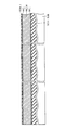
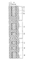
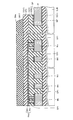
- FIG. 2 is a schematic cross-sectional view taken along a line II-II in FIG.
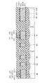
- FIG. 3 is a schematic plan view showing a state of an uppermost surface of the semiconductor chip in FIG. 2.
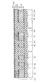
- FIG. 4 is a schematic enlarged plan view of a region surrounded by a round dotted line “IV” in FIG. 3.
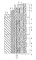
- FIG. 5 is a schematic cross-sectional view taken along a line VV in FIG. 4. It is a schematic sectional drawing which defines the dimension of the thickness direction of each part in FIG.
- the semiconductor chip as the present embodiment is mounted inside a package PK.
- Package PK is arranged on one main surface of printed circuit board PB.
- the package PK is connected to a wiring formed on one main surface of the printed circuit board PB by a lead wire LD that is electrically connected to an internal semiconductor chip.
- microcomputer chip MC1 which is a semiconductor chip having an OCO circuit as the present embodiment is fixed on one main surface of die pad DP by die bond material DB. Conversely, the die pad DP is attached to the lower main surface (second main surface) side of the microcomputer chip MC1.
- the die pad DP is formed of a ceramic material such as aluminum nitride (AlN) having excellent heat dissipation.
- AlN aluminum nitride
- the die bond material DB for example, a paste material such as a silver paste or a resin paste is used. That is, a stacked structure of the die pad DP and the microcomputer chip MC1 is mounted inside the package PK.
- the bonding wire BW is a wiring made of, for example, copper or gold, for electrically connecting the pad opening SP and the lead wire LD. More specifically, the pad opening SP and the bonding wire BW are electrically connected at the connection point B1, and the lead wire LD and the bonding wire BW are electrically connected at the connection point B2.
- the lead wire LD is electrically connected to the wiring formed on one main surface of the printed circuit board PB at the connection point C1.
- the interior of the package PK is filled with a mold resin MR (resin material) made of, for example, phenol.
- the mold resin MR is disposed so as to cover the outer peripheral portion of the laminated structure of the microchip MC1.
- the mold structure MR is arranged so as to cover the uppermost MSF (first main surface) and side surfaces along the main surface of the microchip MC1 and the lowermost surface MBF (opposite the uppermost MSF) of the die pad DP.
- the aspect inside the package PK shown in FIG. 2 is an example to the last, and is not limited to this.
- RAM formation area MC11, CPU formation area MC12, peripheral circuit formation areas MC13 and MC15, ROM formation area MC14, power supply circuit area MC16, and the like are arranged on top surface MSF of microcomputer chip MC1.
- the power supply circuit area MC16 includes a high-speed OCO circuit. This layout configuration is merely an example of a microcomputer chip and is not limited to this.
- this semiconductor device is provided on first interlayer insulating film SO11 provided above substrate SUB, and on first interlayer insulating film SO11, and in a first direction (X in FIG. 4). And a plurality of dummy layers Md extending in a second direction (Y direction in FIG. 4) orthogonal to the first direction (X direction).
- Ma and Mb are provided.
- tap layers Mi, Ma to Mc, and Mo are provided.
- pad layer MP manufactured in the same process as dummy layer Md and tap layers Ma and Mb is provided on first interlayer insulating film SO11.
- the plurality of first dummy layers Md and the tap layers Ma and Mb are covered with a second interlayer insulating film SO12 whose surface is flattened, and a second direction (Y direction) is formed on the second interlayer insulating film SO12. Is provided with a metal resistive element layer Rm2.
- the metal resistance element layer Rm2 has a two-layer structure of a metal wiring layer Rm and an antioxidant film layer SN1.
- a metal contains metals other than a transition metal and a transition metal, and does not contain a semimetal, a semiconductor, and a nonmetal.
- the metal resistive element layers Rm1 to Rm4 are arranged so as to extend in the first direction (X direction) and to have a predetermined gap between each other in the second direction (Y direction). .
- the metal resistance element layers Rm1 to Rm4 are provided with contact plugs CP1 penetrating the second interlayer insulating film SO12 and connected to the tap layers Mi, Ma to Mb, and Mo at both ends.
- a dummy metal resistance element layer Rmd and a dummy tap layer Mde are provided on the outer sides of the metal resistance element layers Rm1 and Rm4.
- the metal resistance element layers Rm1 to Rm4 include the tap layer Mi ⁇ contact plug CP1 ⁇ metal resistance element layer Rm1 ⁇ contact plug CP1 ⁇ tap layer Ma ⁇ contact plug CP1 ⁇ metal resistance element layer Rm2 ⁇ contact plug CP1 ⁇ tap layer.
- metal resistance element layer Rm2 is covered with a third interlayer insulating film SO13 having a flat surface, and this third interlayer insulating film SO13 is covered with a passivation film SN12 having a flat surface.
- the film SN12 is covered with a protective film PF having a flat surface.
- the second interlayer insulating film SO12, the third interlayer insulating film SO13, the passivation film SN12, and the protective film PF located above the plurality of pad layers MP are provided with openings and the pads from which the surface of the pad layer MP is exposed An opening SP is defined.
- the opening end face SPe of the second interlayer insulating film SO12 and the third interlayer insulating film SO13, the opening edge SNe of the passivation film SN12, and the opening end face PFe of the protective film PF are provided so as to be located on the inner side.
- the distance (S1) between the opening end face SPe of the second interlayer insulating film SO12 and the third interlayer insulating film SO13 and the metal resistance element layers Rm1 to Rm4 is the metal resistance element layer Rm1 to Rm4 due to the intrusion of moisture from the opening end face SPe. From the viewpoint of preventing the moisture resistance deterioration of the film, the distance is set to be 100 ⁇ m or more.
- the thickness RTt of the mold resin MR covering the uppermost surface MSF which is the first main surface of the microcomputer chip MC1 is equal to the uppermost surface MBF of the die pad DP (the microcomputer chip MC1
- the thickness RBt of the mold resin MR covering the surface on the opposite side of the surface is preferably 0.54 times or more and 1.31 times or less. In other words, it is preferred that 0.54 ⁇ RTt / RBt ⁇ 1.31.
- the thicknesses RTt and RBt here are average values of the thickness of the mold resin MR formed on all points of the uppermost surface MSF of the microcomputer chip MC1. Moreover, the said thickness can be measured, for example using an ultrasonic thickness measuring instrument etc., without contacting mold resin MR.
- the thickness Ct of the microcomputer chip MC1 is preferably 0.2 mm or more and 0.4 mm or less, and more preferably 0.3 mm or more and 0.4 mm or less.
- the thickness of the microcomputer chip MC1 represents the average value of the thickness including the thickness of the interlayer insulating film SO11, the tap layer Ma, the contact plug CP1, and the like described above.
- the difference between the maximum value and the minimum value of the same microcomputer chip MC1 is preferably 40 ⁇ m or less, and more preferably 20 ⁇ m or less. preferable.
- the average thickness of the die bond DB can be set to 0.03 mm as an example, and the average thickness of the die pad DP can be set to 0.125 mm as an example.
- the average thickness of the entire package PK can be set to 1.4 mm as an example.
- the thickness of the microcomputer chip MC1 In order to adjust the ratio of the thickness RTt to the thickness RBt in order to make the thickness RTt 0.54 to 1.31 times the thickness RBt as described above, the thickness of the microcomputer chip MC1, the thickness of the die bond DB, It is conceivable to appropriately change each of the thicknesses of the die pad DP. However, the thickness of the microcomputer chip MC1 can be changed more easily than the die pad DP and the die bond DB. For example, the microcomputer chip MC1 having a thickness of 300 ⁇ m and the microchip MC1 having a thickness of 400 ⁇ m can be formed using the same mold.
- Cx> Cy may be satisfied, or Cx ⁇ Cy may be satisfied.
- the package PK (mold resin MK) also has a rectangular shape in plan view
- the dimension Cx in the first direction (X direction) in plan view of the microcomputer chip MC1 is a package PK (mold resin) having a rectangular shape in plan view.
- MR is preferably 0.16 to 0.4 times the dimension Px in the first direction (X direction). In other words, 0.16 ⁇ Cx / Px ⁇ 0.4 is preferable.
- the dimension Cy in the second direction (Y direction) in plan view of the microcomputer chip MC1 is 0.16 times or more the dimension Py of the package PK in the second direction (Y direction). It is preferably 0.4 times or less. In other words, it is preferable that 0.16 ⁇ Cy / Py ⁇ 0.4.
- the die pad DP also has a rectangular shape in plan view, and the dimension DPx in the first direction in plan view of the die pad DP is the package PK (mold resin MR) in the first direction (X direction). It is preferably 0.5 times or more and 1.5 times or less of the dimension Px. In other words, it is preferable that 0.5 ⁇ DPx / Px ⁇ 1.5. That is, DPx> Px or DPx ⁇ Px.
- the dimension DPy in the second direction in plan view of the die pad DP is not less than 0.5 times and not more than 1.5 times the dimension Py of the package PK in the second direction (Y direction). It is preferable that In other words, it is preferable that 0.5 ⁇ DPy / Py ⁇ 1.5. That is, DPy> Py may be satisfied, or DPy ⁇ Py may be satisfied.
- the mold resin MR used in the present embodiment preferably has a Young's modulus of 18000 MPa or more and 30000 MPa or less.
- the mold resin MR preferably has a linear expansion coefficient of 8 ⁇ 10 ⁇ 6 / ° C. or more and 12 ⁇ 10 ⁇ 6 / ° C. or less.
- the glass transition temperature of the mold resin MR is preferably 100 ° C. or higher and 150 ° C. or lower.
- the inventor of the present invention after earnest research, changes the resistance value of the metal resistive element layers Rm1 to Rm4 by setting the average value of the thickness RTt to 0.54 times or more and 1.31 times or less of the average value of the thickness RBt. It was found that can be reduced. By reducing the fluctuation of the resistance values of the metal resistive element layers Rm1 to Rm4, the fluctuation of the oscillation frequency of the OCO circuit can be reduced, and the accuracy of the oscillation frequency of the circuit can be further improved.
- the inventors of the present invention similarly set the resistance values of the metal resistive element layers Rm1 to Rm4 by setting the dimensions of the respective parts such as the microcomputer chip MC1 and the package PK and the physical properties of the mold resin MR within the above numerical ranges. It has been found that the fluctuation of can be reduced. By reducing the fluctuation of the resistance values of the metal resistive element layers Rm1 to Rm4, the fluctuation of the oscillation frequency of the OCO circuit can be reduced, and the accuracy of the oscillation frequency of the circuit can be further improved.
- first interlayer insulating film SO11 having a planarized surface is formed.
- the substrate SUB a substrate having a thickness of 0.6 mm or more and 0.9 mm or less is used so that the thickness of the microcomputer chip MC1 finally formed is 0.2 mm or more and 0.4 mm or less. It is preferable. That is, when the substrate SUB having a thickness of 0.6 mm or more and 0.9 mm or less is used, it is preferable to remove a certain thickness from the lowermost surface of the substrate SUB by polishing as will be described later. By using the substrate SUB that is thicker than the microcomputer chip MC1 that is finally formed, the occurrence of cracks and distortions in the substrate SUB can be suppressed.
- a silicon oxide film is used for the first interlayer insulating film SO11.
- a high density plasma CVD USG (Undope Silicate Glass) film (HDP-USG) formed by the CVD method and a TEOS film (P-TEOS) formed by the plasma CVD method are used.
- the substrate SUB may be a semiconductor substrate in which a semiconductor element is formed, or may be a substrate made of a material other than a semiconductor.
- the wiring layer M is the uppermost aluminum wiring and is formed by sputtering.
- the wiring layer M has a laminated structure including a TiN / Ti film as the lower layer M1, a copper-added aluminum (Al—Cu) film as the wiring body M2, and a TiN / Ti film as the upper layer M3.
- the film thickness of the wiring layer M is about several hundred nm to 1 ⁇ m.
- an antireflection film SON11 is formed on the wiring layer M.
- a plasma oxynitride film P-SiON
- CVD chemical vapor deposition
- the wiring layer M and the antireflection film SON11 are patterned.
- photolithography and dry etching are used for the patterning. Accordingly, the plurality of dummy layers Md arranged in the first direction (X direction) so as to have a predetermined gap between each other and extending in the second direction (Y direction) orthogonal to the first direction (X direction) and The tap layers Ma and Mb arranged at positions sandwiching the plurality of dummy layers Md from both sides in the first direction (X direction) and the pad region layer Mp are formed.
- second interlayer insulating film SO12 is formed to cover dummy layer Md, tap layers Ma and Mb, and pad region layer Mp.
- a silicon oxide film made of HDP-USG and P-TEOS is used for the second interlayer insulating film SO12.
- the surface of the silicon oxide film is planarized by a CMP (Chemical-Mechanical-Polishing) method.
- the HDP-USG film needs to have a film thickness of 1 ⁇ m or more in order to cover the aluminum wiring step, and the flattening polishing amount needs to be about 1.5 times the step.
- the dummy layer Md has the same interval, for example, a line width of about 3 ⁇ m and a space of about 3 ⁇ m in order to improve the flatness of the metal resistance element layer Rm to be formed later.
- contact holes Va1 communicating with each of the tap layers Ma and Mb are formed in the second interlayer insulating film SO12 using photolithography and dry etching. It is preferable to provide two or more contact holes Va1 on one side in order to ensure the stability of contact resistance.
- a contact plug CP1 is formed in the contact hole Va1.
- a TiN / Ti laminated film CP11 is formed as a barrier metal by a sputtering method, and then a tungsten (W) film CP12 is formed by a CVD method. Thereafter, the upper surfaces of the TiN / Ti stacked film CP11 and the tungsten (W) film CP12 are flattened by CMP.
- the metal resistance element layer Rm2 is formed on the second interlayer insulating film SO12.
- the metal resistance element layer Rm2 has a two-layer structure of a metal wiring layer Rm and an antioxidant film layer SN1. It is preferable to use a refractory metal for the metal wiring layer Rm.
- the refractory metal is generally a metal having a melting point of 1500 ° C. or higher.
- Group 6 Cr (chromium), Mo (molybdenum), W (tungsten), Group 5 V (vanadium), Nb (niobium), Ta (Tantalum), Group 4 Ti (titanium), Zr (zirconium) and the like are included.
- a TiN film is formed by a sputtering method.
- the film is formed to a thickness of about 30 nm, for example.
- an oscillation circuit such as an OCO circuit is formed using a refractory metal because it generates a large amount of heat during use.
- TiN which is a refractory metal material
- the present invention is not limited to this material.
- a resistance material used for a metal wiring layer has a lower specific resistance than a semiconductor material such as polysilicon. Therefore, a circuit that requires a certain amount of resistance (for example, an OCO circuit) is conventionally formed of polysilicon.
- a metal resistive material for a circuit (for example, an OCO circuit)
- the number of sheets needs to be very large in order to obtain a resistance value equivalent to that of polysilicon, and there is a demerit that the layout area becomes very large. is there. Therefore, a material having a relatively high specific resistance is desirable as the metal resistance material.
- the temperature-to-temperature accuracy of the circuit can be improved when the resistance value variation is smaller within the temperature guarantee range of the semiconductor device product.
- TCR Temperature Coefficient of Resistance
- titanium nitride (TiN) is used as a refractory metal material that satisfies these requirements.
- a laminated film with Ti may be used, or the nitrogen concentration may be changed.
- other materials such as tantalum nitride (TaN) can be used instead of titanium nitride (TiN) to satisfy the above requirements.
- a plasma nitride (P-SiN) film is used as the antioxidant film layer SN1 and is formed by a CVD method.
- the film thickness is about 45 mm, for example.
- the metal resistance element layer Rm2 is patterned by using a photoengraving technique and a dry etching process.
- the metal resistance element layers Rm1 to Rm4 (including the dummy metal resistance element layer Rmd) are patterned in stripes, and the metal resistance element layers Rm1 to Rm4 are By connecting the tap layers Mi, Ma, Mb, Mc, and Mo with the contact plug CP1, the series connection is established.
- the width of the metal resistive element layer Rm is set to about 0.8 ⁇ m in the present embodiment because of a demand for improving the processing dimension stability and a demand for reducing the layout area. Further, the extraction width (resistance interval) is about 0.6 ⁇ m.
- the length of the metal resistive element layer (unit resistance) is desirably about 40 ⁇ m or more.
- the antioxidant film layer SN1 prevents the surface of the metal resistive element layer Rm2 from being exposed to the oxidizing atmosphere when the resist is removed in the oxygen plasma atmosphere.
- a third interlayer insulating film SO13 is formed on second interlayer insulating film SO12 so as to cover metal resistance element layer Rm2.
- the third interlayer insulating film SO13 is formed by a CVD method using a silicon oxide film made of a P-TEOS film.
- a passivation film SN12 is formed on the third interlayer insulating film SO13.
- a P-SiN film is used and is formed by a CVD method.
- the passivation film SN12 is a film for protecting the surface of the semiconductor device from external damage after the wiring process is completed.
- the second interlayer insulating film SO12, the third interlayer insulating film SO13, and the passivation film SN12 are selectively removed by a photoengraving technique and a dry etching process to form one of the pad region layers MP.
- a pad opening SP that exposes the portion is formed.
- the opening edge SNe of the passivation film SN12 is more than the opening end face SPe of the second interlayer insulating film SO12 and the third interlayer insulating film SO13. Has also retreated.
- a photosensitive polyimide film is applied as a protective film PF on the passivation film SN12, and a polyimide pattern is formed through photolithography.
- the opening end face PFe of the protective film PF recedes from the opening edge SNe of the passivation film SN12.
- a desired thickness is polished and removed from the lowermost surface of the substrate SUB with a grinder. Then remove the surface protection tape. It is preferable that the thickness of the entire substrate SUB on which the circuit is formed, which is finally formed after the substrate SUB is polished and removed, is 0.2 mm or more and 0.4 mm or less.
- the microcomputer chip MC1 shown in FIGS. 2 and 3 is completed.
- the die pad DP is bonded and fixed on the main surface (opposing the main surface MSF on which the circuit is formed) of the microcomputer chip MC1 using the die bond material DB.
- the pad opening SP of the microcomputer chip MC1 and the lead wire LD of the package PK are electrically connected by a bonding wire BW made of, for example, gold or copper.
- an assembly process is performed in which the laminated structure of the microchip MC1 is mounted inside the package PK, and the mold resin MR is filled so as to cover the outer peripheral portion of the laminated structure.
- the laminated structure is preferably arranged in the package PK at a position where the mold resin MR satisfies the above-described relationship of 0.54 ⁇ RTt / RBt ⁇ 1.31.
- the die pad thickness DPt die bond thickness DBt
- package thickness Pt etc.
- it is easier to change the chip thickness Ct than the die pad thickness DPt, die bond thickness DBt, package thickness Pt, and resin thickness RBt due to technical restrictions in the assembly process and the package PK specifications. That is, it is preferable to adjust the ratio between RTt and RBt by changing the chip thickness Ct and the resin thickness RTt after fixing the resin thickness RBt and the die pad thickness DBt.
- the semiconductor device in the package PK state shown in FIGS. 1 and 2 is completed by performing the assembly process after adjusting the dimensions of each part to be within a desired range as described above.
- This oscillating circuit is an oscillating circuit that generates an output signal having a predetermined oscillation period by, for example, an oscillating operation by repeatedly charging and discharging a capacitive element.
- a constant current circuit CVC including a depletion-type first MOSFET Q1, a resistor R1 having a small resistance value (configured in the above-described metal resistance element layer Rm), an enhancement-type second MOSFET Q2, a third MOSFET Q3, and a fourth MOSFET Q4, and enhancement-type MOSFETs Q5 ⁇ MOSFET Q7, capacitor C1 (capacitance element), differential amplifier circuit DAC, delay circuit DC, and booster circuit PRC.
- the source of the MOSFET Q1 and one end of the resistor R1, the drain of the MOSFET Q1 and the drain of the MOSFET Q2, the gate and drain of the MOSFET Q2, the gate of the MOSFET Q3, the drain of the MOSFET Q3 and the drain of the MOSFET Q4, the gate and drain of the MOSFET Q4, and the MOSFET Q1 The gate, the sources of the MOSFETs Q2 and Q3, the power supply voltage Vcc, the other end of the resistor R1, and the source of the MOSFET Q4 and the ground voltage are respectively connected.
- MOSFET Q1 and MOSFET Q4 have an N channel MOS structure
- MOSFET Q2 and MOSFET Q3 have a P channel MOS structure.
- the gate of the MOSFET Q5 whose source is connected to the power supply voltage Vcc is connected to the connection node between the gate of the MOSFET Q2 and the gate of the MOSFET Q3 of the constant current circuit CVC. Further, the drain of the MOSFET Q5 is the source of the MOSFET Q6 and the drain of the MOSFET Q6 is The drain of the MOSFET Q7 and the source of the MOSFET Q7 are connected to the ground voltage.
- the gate of the MOSFET Q6 and the gate of the MOSFET Q7 are connected in common and connected to the output terminal of the delay circuit DC.
- a connection node between the drain of the MOSFET Q6 and the drain of the MOSFET Q7 is connected to one end of the capacitor C1 and the positive input terminal of the differential amplifier circuit DAC.
- the constant voltage level generated in the constant current circuit CVC is compared with the voltage level of the capacitor C1, and the capacitor C1 is charged or discharged according to the comparison result.
- the step-up circuit PRC has an inverter IV1, enhancement type n-channel MOSFETs Q12 and Q13, and capacitors C2 and C3.
- the start-up signal CLK is input and the boosted output voltage is applied to the gate of the MOSFET Q4 of the constant current circuit CVC and the MOSFET Q1. Applied to the connection node with the gate.
- the start signal CLK is input to the gates of the inverter IV1 and the MOSFET Q12, the output terminal of the inverter IV1, one end of the capacitor C2, the other end of the capacitor C2, the drain of the MOSFET Q12, the gate and drain of the MOSFET Q13, the MOSFET Q13.
- the source of the MOSFET Q12 and the other end of the capacitor C3 are connected to the ground voltage.
- the graph of FIG. 19 shows the fluctuation ratio of the resistance value of the metal resistance element layer Rm of the OCO circuit when the ratio of RTt and RBt in the present embodiment shown in FIG. 1 and FIG. 2 is changed.
- the horizontal axis of the graph of FIG. 19 indicates the ratio (RTt / RBt) between RTt and RBt.
- the vertical axis of the graph of FIG. 19 indicates the variation rate of the resistance value of the resistance element layer Rm made of titanium nitride (TiN) when the semiconductor device is used.
- the fluctuation rate of the resistance value is, for example, the resistance of the metal resistance element layer Rm after applying a thermal load by soldering, reliability test, or the like on the basis of the resistance value of the metal resistance element layer Rm immediately after the assembly process. Indicates the rate of change of the value.
- the curve in the graph of FIG. 19 shows the calculation result by the simulation using the model of the semiconductor device in this embodiment. Further, the data indicated by dots in the graph of FIG. 19 indicates the result of actual measurement of the semiconductor device according to the present embodiment manufactured as a prototype.
- a package PK having a square shape with a side of 12 mm in plan view and a thickness Pt (see FIG. 6) of 1.4 mm was used.
- the die pad DP had a thickness DPt (see FIG. 6) of 0.125 mm and a size DPx and DPy (see FIG. 7) in plan view of 3 mm.
- the thickness of the die bond DB is 0.03 mm.
- the microcomputer chip MC1 has a square with a side length of 7 mm in plan view, and its thickness Ct (see FIG. 6) is changed according to a change in the value of RTt / RBt, for example, 0.3 mm. Yes.
- the ratio of the sizes Cx and Cy (see FIG. 7) of the microcomputer chip MC1 is 1, the value of DPx / Cx (DPy / Cy) is 0.429, and the value of Cx / Px is 0.583.
- the average value of Young's modulus of the mold resin MR was 20874 MPa, the average value of the linear expansion coefficient of the mold resin MR was 11 ⁇ 10 ⁇ 6 / ° C., and the glass transition temperature of the mold resin MR was 125 ° C.
- the Young's modulus of the mold resin MR can be calculated, for example, by measuring the deflection amount of the mold resin MR using a Ewing apparatus.
- the linear expansion coefficient of the mold resin MR can be measured, for example, by raising the temperature of a rod-shaped test piece of the mold resin MR at a constant speed.
- the glass transition temperature of the mold resin MR can be derived by measuring physical properties such as hardness and heat quantity of the resin while changing the temperature.
- the curve showing the calculation result shows that when RTt / RBt is about 1, the resistance value fluctuation of the metal resistance layer Rm shows the maximum value.
- the maximum value is about ⁇ 0.15%, and at this time, the absolute value of the resistance value fluctuation of Rm is the minimum. Even if RTt / RBt becomes larger or smaller than 1, the value of the resistance value fluctuation becomes small (the absolute value of the resistance value fluctuation becomes large).
- the resistance value fluctuation value is ⁇ 0.200%. In the region outside the range of 0.54 ⁇ RTt / RBt ⁇ 1.31, it is within the range.
- the slope of the graph is larger than that of the area. In other words, in the region outside the range of approximately 0.54 ⁇ RTt / RBt ⁇ 1.31, the absolute value of the resistance value fluctuation is larger than that in the region within the range.
- the resistance value variation is ⁇ 0.200% or more and + 0.200% or less (the absolute value of the resistance value variation is 0.200%) It is preferable that
- the present invention can be applied particularly advantageously to a semiconductor device including an oscillation circuit having a refractory metal on a semiconductor chip.
Landscapes
- Semiconductor Integrated Circuits (AREA)
Abstract
発振回路に含まれる抵抗素子層の抵抗値をより高精度に制御することにより、発振回路の発振周波数の精度を高めることが可能な本半導体装置は、高融点金属からなる金属抵抗素子層(Rm2)を有する発振回路を含み、かつ互いに対向する第1の主面(MSF)および第2の主面を有する半導体チップ(MC1)と、半導体チップ(MC1)の第2の主面側に取り付けられたダイパッド(DP)と、半導体チップ(MC1)およびダイパッド(DP)を覆うように形成された樹脂材料(MR)とを備えている。上記半導体チップ(MC1)の第1の主面(MSF)上を覆う樹脂材料(MR)の厚みは、ダイパッド(DP)の半導体チップ(MC1)側とは反対側の表面(MBF)上を覆う樹脂材料(MR)の厚みの0.54倍以上1.31倍以下である。
Description
本発明は半導体装置に関し、特に、発振回路を有する半導体装置に関するものである。
従来、マイコン製品と発振子とは別構造であったが、近年、マイコンチップ内に発振子を内蔵することで、レイアウト面積の縮小、コスト低減等が図られるようになってきている。マイコンチップ内に発振子を内蔵するには、あらゆる環境下(電圧・温度)で安定した発振周波数を出力する必要があり、マイコン製品の高速OCO(On Chip Oscillator)回路と呼ばれる、マイコンチップの上に発振用素子が組み込まれた構成を有する発振回路では、目標精度として、たとえば40MHz±1%を達成することが求められている。
一般に、アナログ回路である高速OCO回路が安定した発振周波数を出力するためには、OCO回路は大きな抵抗値を有し、OCO回路内に定電流が発生する構成を有することが必要である。高速OCO回路内の定電流発生回路の、大きな抵抗値を示すための抵抗体として、たとえば特開平6-318693号公報(特許文献1)に開示される薄膜状の抵抗素子が用いられる。一方、このような薄膜状の抵抗素子が形成されたOCO回路を含む基板は、たとえば特開平6-45478号公報(特許文献2)に開示されるように、その全体がモールド樹脂などの樹脂材料で封止されている。
特開平6-318693号公報における抵抗素子層は、比較的高抵抗の得られる多結晶シリコンの薄膜からなる。しかし多結晶シリコンの抵抗素子層は、いわゆるピエゾ抵抗効果に起因して、応力により抵抗値が変動する。特に、特開平6-45478号公報の電子回路装置のようにモールド樹脂が基板を封止する場合には、パッケージング工程以降のモールド応力による、抵抗素子層の抵抗値の変動が顕著である。抵抗素子層の抵抗値の変動は、高速OCO回路の周波数変動を大きくし、高速OCO回路の目標精度を達成することを困難とする可能性がある。
特開平6-45478号公報の電子回路装置においては、回路基板の一方の主表面側と、一方の主表面に対向する他方の主表面側とのモールド樹脂がほぼ等量とされる。このため回路基板の上記一方および他方の主表面側のモールド樹脂に作用される圧縮応力の大きさがほぼ等しくなる。その結果、回路基板の反りなどの変形が抑制され、当該抵抗素子の抵抗値の変動が抑制される。
しかし特開平6-45478号公報においては、回路基板の配置される位置が、これを封止するケースの厚さ方向の中心部に保持されることのみ記載されている。つまり当該公報においては、ケースの厚さ方向に対する、回路基板の配置される位置の範囲が明確にされていない。このため、特に発振周波数の高精度制御が要求される高速OCO回路に対して当該公報の発明を用いても、抵抗素子の抵抗値の誤差が許容範囲を超え、所望の周波数誤差を達成できなくなる可能性がある。
本発明は、以上の問題に鑑みなされたものである。その目的は、抵抗素子層の抵抗値をより高精度に制御することにより、OCO回路の発振周波数の精度を高めることが可能な半導体装置を提供することである。
本発明の一実施例による半導体装置は以下の構成を備えている。高融点金属からなる金属抵抗素子層を有する発振回路を含み、かつ互いに対向する第1および第2の主面を有する半導体チップと、半導体チップの第2の主面側に取り付けられたダイパッドと、半導体チップおよびダイパッドを覆うように形成された樹脂材料とを備えている。上記半導体チップの第1の主面上を覆う樹脂材料の厚みは、ダイパッドの半導体チップ側とは反対側の表面上を覆う樹脂材料の厚みの0.54倍以上1.31倍以下である。
本実施例によれば、応力が加わった場合であっても、抵抗値が変動しない構造を備える半導体装置を提供することを可能とする。
以下、本発明の実施の形態について図に基づいて説明する。
まず、本実施の形態としてパッケージ状態の半導体装置について説明する。
まず、本実施の形態としてパッケージ状態の半導体装置について説明する。
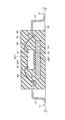
図1を参照して、本実施の形態としての半導体チップは、パッケージPKの内部に搭載されている。パッケージPKは、プリント基板PBの一方の主表面上に配置されている。パッケージPKは、その内部の半導体チップと電気的に接続されるリード線LDにより、プリント基板PBの一方の主表面上に形成された配線と接続されている。
図2を参照して、本実施の形態としての、OCO回路を有する半導体チップであるマイコンチップMC1は、ダイパッドDPの一方の主表面上に、ダイボンド材DBにより固定されている。逆に言えばマイコンチップMC1の下側の主表面(第2の主面)側にダイパッドDPが取り付けられている。ダイパッドDPはたとえば放熱性に優れた、窒化アルミニウム(AlN)などのセラミックス材料により形成される。またダイボンド材DBとしてはたとえば銀ペーストや樹脂ペーストなどのペースト材料が用いられる。すなわちパッケージPKの内部には、ダイパッドDPとマイコンチップMC1との積層構造が搭載されている。
マイコンチップMC1には、後述するマイコンチップMC1に形成された回路と電気的に接続されたパッド開口部SPが形成されている。ボンディングワイヤBWは、パッド開口部SPとリード線LDとを電気的に接続する、たとえば銅や金などからなる配線である。より具体的には、接続点B1においてパッド開口部SPとボンディングワイヤBWとが電気的に接続され、接続点B2においてリード線LDとボンディングワイヤBWとが電気的に接続される。またリード線LDは接続点C1において、プリント基板PBの一方の主表面上に形成された配線と電気的に接続されている。
パッケージPKの内部には、たとえばフェノールからなるモールド樹脂MR(樹脂材料)が充填されている。モールド樹脂MRはマイクロチップMC1の積層構造の外周部を覆うように配置されている。具体的にはモールド構造MRは、マイクロチップMC1の主表面に沿う最上面MSF(第1の主面)や側面、およびダイパッドDPの(最上面MSFに対向する)最下面MBFを覆うように配置されている。なお図2に示すパッケージPKの内部の態様はあくまで一例であり、これに限定したものではない。
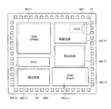
図3を参照して、マイコンチップMC1の最上面MSFには、RAM形成領域MC11、CPU形成領域MC12、周辺回路形成領域MC13,MC15、ROM形成領域MC14、および電源回路領域MC16などが配置される。電源回路領域MC16は、高速OCO回路を含んでいる。なお、本レイアウト構成はあくまでマイコンチップの一例であり、これに限定したものではない。
次に、図4および図5を参照して、マイコンチップMC1に形成された回路の一例として、高速OCO回路の一部構造について説明する。
図5を参照して、この半導体装置は、基板SUBの上方に設けられた第1層間絶縁膜SO11と、この第1層間絶縁膜SO11の上に設けられ、第1方向(図4中のX方向)において相互に所定の間隙を有するように配置され、第1方向(X方向)に対して直交する第2方向(図4中のY方向)に延びる複数のダミー層Mdを有する。
第1層間絶縁膜SO11の上には、複数のダミー層Mdを第1方向(X方向)において両側から挟む位置に、第2方向(Y方向)において所定の間隙を隔てて配置されるタップ層Ma,Mbが設けられている。図4に示す平面視においては、タップ層Mi,Ma~Mc,Moが設けられている。
図5を参照して、第1層間絶縁膜SO11の上には、ダミー層Mdおよびタップ層Ma,Mbと同一工程で製造されたパッド層MPが設けられている。
複数の第1ダミー層Mdおよびタップ層Ma,Mbは、表面が平坦化された第2層間絶縁膜SO12に覆われ、この第2層間絶縁膜SO12の上には、第2方向(Y方向)に延びる金属抵抗素子層Rm2が設けられている。金属抵抗素子層Rm2は、金属配線層Rmと酸化防止膜層SN1との2層構造を有している。なお、金属とは、遷移金属および遷移金属以外の金属を含み、かつ、半金属、半導体、および、非金属を含まない。
図4に示す平面視においては、金属抵抗素子層Rm1~Rm4は、それぞれ第1方向(X方向)に延び、第2方向(Y方向)において相互に所定の間隙を有するように配置されている。金属抵抗素子層Rm1~Rm4は、それぞれの両端部において、第2層間絶縁膜SO12を貫通しタップ層Mi,Ma~Mb,Moに連結するコンタクトプラグCP1が設けられている。
なお、写真製版技術における製造精度を向上させる観点から、金属抵抗素子層Rm1およびRm4のそれぞれの外側には、ダミー金属抵抗素子層Rmd、およびダミータップ層Mdeが設けられている。
これにより、金属抵抗素子層Rm1~Rm4は、タップ層Mi→コンタクトプラグCP1→金属抵抗素子層Rm1→コンタクトプラグCP1→タップ層Ma→コンタクトプラグCP1→金属抵抗素子層Rm2→コンタクトプラグCP1→タップ層Mb→コンタクトプラグCP1→金属抵抗素子層Rm3→コンタクトプラグCP1→タップ層Mc→コンタクトプラグCP1→金属抵抗素子層Rm4→コンタクトプラグCP1→タップ層Moと電気的に接続された直列接続となる。
図5を参照して、金属抵抗素子層Rm2は、表面が平坦な第3層間絶縁膜SO13に覆われ、この第3層間絶縁膜SO13は、表面が平坦なパッシベーション膜SN12により覆われ、このパッシベーション膜SN12は、表面が平坦な保護膜PFにより覆われている。
複数のパッド層MPの上方に位置する第2層間絶縁膜SO12、第3層間絶縁膜SO13、パッシベーション膜SN12、および保護膜PFには、開口部が設けられ、パッド層MPの表面が露出するパッド開口部SPが規定される。第2層間絶縁膜SO12および第3層間絶縁膜SO13の開口端面SPe、パッシベーション膜SN12の開口エッジSNe、および保護膜PFの開口端面PFeは、それぞれ内部側に位置するように設けられている。
第2層間絶縁膜SO12および第3層間絶縁膜SO13の開口端面SPeと、金属抵抗素子層Rm1~Rm4との距離(S1)は、開口端面SPeからの水分の浸入による金属抵抗素子層Rm1~Rm4の耐湿劣化を阻止する観点から、100μm以上離れるように設けられている。
なお、第1層間絶縁膜SO11の下層には、公知の構造の多層配線構造が採用されている。
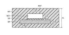
次に、図6および図7を参照して、本実施の形態におけるマイコンチップMC1やダイパッドDPなどの各部分の寸法について説明する。
図6を参照して、本実施の形態においては、マイコンチップMC1の第1の主面である最上面MSF上を覆うモールド樹脂MRの厚みRTtは、ダイパッドDPの最下面MBF上(マイコンチップMC1とは反対側の表面上)を覆うモールド樹脂MRの厚みRBtの0.54倍以上1.31倍以下であることが好ましい。言い換えれば、0.54≦RTt/RBt≦1.31であることが好ましい。ここでの厚みRTt,RBtとは、マイコンチップMC1の最上面MSFのすべての点の上に形成されるモールド樹脂MRの厚みの平均値である。また当該厚みは、たとえば超音波厚み測定器などを用いて、モールド樹脂MRに接することなく測定することができる。
マイコンチップMC1の厚みCtは、0.2mm以上0.4mm以下であることが好ましく、なかでも0.3mm以上0.4mm以下であることがより好ましい。ここでマイコンチップMC1の厚みとは、上述した層間絶縁膜SO11やタップ層Ma、コンタクトプラグCP1などの厚みを含めた厚みの平均値を表わすものとする。またたとえばマイコンチップMC1の平均の厚みCtが400μmである場合に、同一のマイコンチップMC1における当該厚みの最大値と最小値との差は40μm以下であることが好ましく、20μm以下であることがより好ましい。
ダイボンドDBの平均の厚みは一例として0,03mm、ダイパッドDPの平均の厚みは一例として0.125mmとすることができる。パッケージPK全体の平均の厚みは一例として1.4mmとすることができる。
上記のように厚みRTtを厚みRBtの0.54倍以上1.31倍以下とするために厚みRTtと厚みRBtとの比率を調整するためには、マイコンチップMC1の厚み、ダイボンドDBの厚み、ダイパッドDPの厚みのそれぞれを適宜変更することが考えられる。しかしダイパッドDPやダイボンドDBよりも、マイコンチップMC1の方が容易に厚みを変更できる。たとえば厚みが300μmのマイコンチップMC1と厚みが400μmのマイクロチップMC1とは、同一の金型を用いて形成することができる。
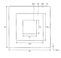
図7を参照して、本実施の形態においては、平面視において矩形状を有するマイコンチップMC1の矩形の1辺に沿う第1方向(図7のX方向)の寸法Cxと、第1方向(X方向)に直交する第2方向(図7のY方向)との寸法Cyの比は1以上1.25以下であることが好ましい。ここではCx>Cyであってもよいし、Cx<Cyであってもよい。パッケージPK(モールド樹脂MK)も平面視において矩形状を有しており、マイコンチップMC1の平面視における第1方向(X方向)の寸法Cxは、平面視において矩形状を有するパッケージPK(モールド樹脂MR)の第1方向(X方向)における寸法Pxの0.16倍以上0.4倍以下であることが好ましい。言い換えれば0.16≦Cx/Px≦0.4であることが好ましい。第2方向(Y方向)についても同様に、マイコンチップMC1の平面視における第2方向(Y方向)の寸法Cyは、第2方向(Y方向)におけるパッケージPKの寸法Pyの0.16倍以上0.4倍以下であることが好ましい。言い換えれば0.16≦Cy/Py≦0.4であることが好ましい。
本実施の形態においては、ダイパッドDPも平面視において矩形状を有しており、ダイパッドDPの平面視における第1方向の寸法DPxは、第1方向(X方向)におけるパッケージPK(モールド樹脂MR)の寸法Pxの0.5倍以上1.5倍以下であることが好ましい。言い換えれば0.5≦DPx/Px≦1.5であることが好ましい。すなわちDPx>Pxであってもよいし、DPx<Pxであってもよい。第2方向(Y方向)についても同様に、ダイパッドDPの平面視における第2方向の寸法DPyは、第2方向(Y方向)におけるパッケージPKの寸法Pyの0.5倍以上1.5倍以下であることが好ましい。言い換えれば0.5≦DPy/Py≦1.5であることが好ましい。すなわちDPy>Pyであってもよいし、DPy<Pyであってもよい。
また、本実施の形態において用いられるモールド樹脂MRは、ヤング率が18000MPa以上30000MPa以下であることが好ましい。モールド樹脂MRは、線膨張係数が8×10⁻⁶/℃以上12×10-6/℃以下であることが好ましい。モールド樹脂MRのガラス転移温度は、100℃以上150℃以下であることが好ましい。
本発明の発明者は鋭意研究の末、厚みRTtの平均値を厚みRBtの平均値の0.54倍以上1.31倍以下とすることにより、金属抵抗素子層Rm1~Rm4の抵抗値の変動を小さくすることができることを見出した。金属抵抗素子層Rm1~Rm4の抵抗値の変動を小さくすることにより、OCO回路の発振周波数の変動を小さくすることができ、当該回路の発振周波数の精度をより高めることができる。
また本発明の発明者は同様に、マイコンチップMC1やパッケージPKなどの各部分の寸法およびモールド樹脂MRの物性値を上記の数値範囲とするとすることにより、金属抵抗素子層Rm1~Rm4の抵抗値の変動を小さくすることができることを見出した。金属抵抗素子層Rm1~Rm4の抵抗値の変動を小さくすることにより、OCO回路の発振周波数の変動を小さくすることができ、当該回路の発振周波数の精度をより高めることができる。
次に、図8~図17を参照して、図4および図5に示すマイコンチップMC1の製造方法について説明する。
図8を参照して、基板SUBの上に、公知の多層配線構造が形成された後、表面が平坦化された第1層間絶縁膜SO11を形成する。ここで、基板SUBは、成膜を行ない最終的に形成されるマイコンチップMC1の厚みが0.2mm以上0.4mm以下となるような厚みとして、0.6mm以上0.9mm以下のものを用いることが好ましい。つまり0.6mm以上0.9mm以下の厚みを有する基板SUBを用いた場合には、後述するように後工程において基板SUBの最下面から一定の厚み分を研磨により除去することが好ましい。最終的に形成されるマイコンチップMC1よりも厚い基板SUBを用いることにより、基板SUBにおける割れや歪みの発生を抑制することができる。
第1層間絶縁膜SO11には、シリコン酸化膜を用いる。シリコン酸化膜には段差被覆性の良いHigh Density Plasma CVD法により成膜したUSG(Undope Silicate Glass)膜(HDP-USG)およびプラズマCVD法により成膜したTEOS膜(P-TEOS)を用いる。なお、基板SUBは、半導体素子が作り込まれた半導体基板でもよく、また、半導体以外の材質よりなる基板であってもかまわない。
次に、第1層間絶縁膜SO11の上に配線層Mを形成する。配線層Mは、最上層アルミ配線であり、スパッタリング法で成膜する。配線層Mは、下層M1としてTiN/Ti膜、配線本体M2として銅添加アルミ(Al-Cu)膜、上層M3としてTiN/Ti膜からなる積層構造である。配線層Mの膜厚は、数百nmから1μm程度である。
次に、配線層Mの上に、反射防止膜SON11を形成する。反射防止膜SON11として、プラズマ酸窒化膜(P-SiON)をCVD法により形成する。
次に、図9を参照して、配線層Mおよび反射防止膜SON11のパターニングを行なう。パターニングには、写真製版技術およびドライエッチング処理を用いる。これにより、第1方向(X方向)において相互に所定の間隙を有するように配置され、第1方向(X方向)に対して直交する第2方向(Y方向)に延びる複数のダミー層Mdと、複数のダミー層Mdを第1方向(X方向)において両側から挟む位置に配置されるタップ層Ma,Mbと、パッド領域層Mpとが形成される。
次に、図10を参照して、ダミー層Md、タップ層Ma,Mb、およびパッド領域層Mpを覆う第2層間絶縁膜SO12を形成する。第2層間絶縁膜SO12には、HDP-USGおよびP-TEOSからなるシリコン酸化膜を用いる。シリコン酸化膜の表面は、CMP(Chemical Mechanical Polishing)法により平坦化処理を行なう。
ここで、HDP-USG膜としてはアルミ配線段差を被覆するために1μm以上の膜厚が必要であり、また平坦化研磨量としては段差の約1.5倍が必要となる。このとき上記ダミー層Mdは、後に成膜される金属抵抗素子層Rmの平坦性を良好にするために同一間隔、たとえば約3μmのライン幅、約3μmのスペースとしている。
次に、図11を参照して、写真製版技術およびドライエッチング処理を用いて、タップ層Ma,Mbのそれぞれに連通するコンタクトホールVa1を、第2層間絶縁膜SO12に形成する。コンタクトホールVa1は、コンタクト抵抗の安定性を確保するため、片側に2箇所以上設けることが好ましい。
次に、図12を参照して、コンタクトホールVa1内に、コンタクトプラグCP1を形成する。コンタクトホールVa1内には、バリアメタルとしてTiN/Ti積層膜CP11をスパッタリング法により成膜し、その後、タングステン(W)膜CP12をCVD法により成膜する。その後、CMP法により、TiN/Ti積層膜CP11およびタングステン(W)膜CP12の上面を平坦にする。
次に、図13を参照して、第2層間絶縁膜SO12の上に金属抵抗素子層Rm2を形成する。金属抵抗素子層Rm2は、金属配線層Rmと酸化防止膜層SN1との2層構造を有している。金属配線層Rmには、高融点金属を用いることが好ましい。高融点金属とは、一般に融点が1500℃以上の金属であり、たとえば6族のCr(クロム)、Mo(モリブデン)、W(タングステン)、5族のV(バナジウム)、Nb(ニオブ)、Ta(タンタル)、4族のTi(チタン)、Zr(ジルコニウム)などが含まれる。金属配線層Rmとしてはこれらのうち、一例として、TiN膜をスパッタリング法により形成する。抵抗素子として約40Ω/□の抵抗値を得るために、たとえば約30nmの膜厚に成膜する。
一般にOCO回路などの発振回路は、使用時の発熱量が大きいため、高融点金属を用いて形成される。上記においては、金属配線層Rmの一例として、高融点金属材料であるTiNを用いた場合について説明しているが、この材料に限定されるものではない。一般に金属配線層に用いられる抵抗材料はポリシリコンなどの半導体材料と比較して比抵抗が低い。よって、ある程度高抵抗を必要とする回路(たとえばOCO回路等)では、従来ポリシリコンで形成していた。
しかし、回路(たとえばOCO回路等)に金属の抵抗材料を使用すると、ポリシリコンと同等の抵抗値を得るために、シート数を非常に大きくする必要があり、レイアウト面積が非常に大きくなるデメリットがある。そこで、金属の抵抗材料としては、中でも比較的比抵抗の高い材料が望ましい。一方、高精度素子として使用する場合、半導体装置製品の温度保証範囲内で抵抗値の変動が小さい方が、回路の温度間精度を向上することができる。
よって、金属の抵抗材料としては、抵抗温度係数(TCR:Temperature Coefficient of Resistance)がなるべく小さい材料が望ましい。
これらの要求を満たす高融点金属材料として、本実施の形態では、窒化チタン(TiN)を用いている。抵抗値の調整のために、Tiとの積層膜にしたり、窒素濃度を変更させるのもよい。また、上記要求を満たすものとして、窒化チタン(TiN)に代わり窒化タンタル(TaN)などの他材料でも適用は可能である。
酸化防止膜層SN1には、プラズマ窒化(P-SiN)膜を用い、CVD法により成膜
する。膜厚は、たとえば約45mmである。
する。膜厚は、たとえば約45mmである。
次に、図14を参照して、写真製版技術およびドライエッチング処理を用いて、金属抵抗素子層Rm2のパターニングを行なう。
この工程により、図4の平面図に示すように、金属抵抗素子層Rm1~Rm4(ダミー金属抵抗素子層Rmdを含む)は、ストライプ状にパターニングが行なわれるとともに、金属抵抗素子層Rm1~Rm4は、コンタクトプラグCP1を介在させてタップ層Mi,Ma,Mb,Mc,Moと電気的に接続されることにより直列接続となる。
金属抵抗素子層Rmの幅としては、加工寸法安定性向上の要求、およびレイアウト面積縮小の要求から、本実施の形態では約0.8μmとしている。また、抜き幅(抵抗間隔)は、約0.6μmである。
直列に繋ぐ単位抵抗の本数、および単位抵抗の長さは必要抵抗値から決まるが、単位抵抗長に関しては極端に短いと、総抵抗にしめるタップ層の影響が大きくなりすぎ抵抗精度が悪くなる。よって、金属抵抗素子層(単位抵抗)の長さは、約40μm以上にすることが望ましい。
なお、酸化防止膜層SN1は酸素プラズマ雰囲気でレジスト除去を行なう際に、金属抵抗素子層Rm2の表面が酸化雰囲気にさらされるのを防止している。
次に、図15を参照して、金属抵抗素子層Rm2を覆うように、第2層間絶縁膜SO12の上に第3層間絶縁膜SO13を形成する。第3層間絶縁膜SO13には、P-TEOS膜からなるシリコン酸化膜を用い、CVD法により形成する。
次に、第3層間絶縁膜SO13の上にパッシベーション膜SN12を形成する。パッシベーション膜SN12には、P-SiN膜を用い、CVD法により成膜する。パッシベーション膜SN12は、配線工程が完了した後に、半導体装置の表面を外的な損傷から保護するための被膜である。
次に、図16を参照して、写真製版技術およびドライエッチング処理により、第2層間絶縁膜SO12、第3層間絶縁膜SO13、およびパッシベーション膜SN12を選択的に除去し、パッド領域層MPの一部が露出するパッド開口部SPを形成する。パッシベーション膜SN12のドライエッチング処理においては、等方性エッチングを用いていることから、パッシベーション膜SN12の開口エッジSNeの方が、第2層間絶縁膜SO12および第3層間絶縁膜SO13の開口端面SPeよりも後退している。
次に、図17を参照して、パッシベーション膜SN12の上に、保護膜PFとして感光性ポリイミド膜を塗布し、写真製版処理を経てポリイミドパターンが形成される。保護膜PFの開口端面PFeは、パッシベーション膜SN12の開口エッジSNeよりも後退している。以上の工程により、図4および図5に示す、基板SUBの主表面上に形成される回路が完成する。
基板SUBの主表面上に形成された回路の最上面(表面)に表面保護テープを貼った後、基板SUBの最下面から所望の厚み分がグラインダで研磨除去される。そして表面保護テープを剥がす。基板SUBが研磨除去された後に最終的に形成される、回路が形成された基板SUB全体の厚みが0.2mm以上0.4mm以下となることが好ましい。
回路が完成した基板SUBをダイシングすることにより、図2および図3に示すマイコンチップMC1が完成する。次にダイボンド材DBを用いて、マイコンチップMC1の(回路が形成された主表面MSFに対向する)主表面上にダイパッドDPを接着固定する。マイコンチップMC1のパッド開口部SPとパッケージPKのリード線LDとが、図2に示すようにたとえば金または銅からなるボンディングワイヤBWにより電気的に接続される。その後、マイクロチップMC1の積層構造がパッケージPKの内部に搭載され、積層構造の外周部を覆うようにモールド樹脂MRが充填される、アセンブリ工程がなされる。
アセンブリ工程において、積層構造は、パッケージPKの内部において、モールド樹脂MRが上述した0.54≦RTt/RBt≦1.31の関係を満足するような位置に配置されることが好ましい。RTt/RBtを上記の比率とするために、図6に示すチップ厚みCtのほか、ダイパッド厚みDPt、ダイボンド厚みDBt、パッケージ厚みPtなどを変更することが考えられる。しかしアセンブリ工程における技術上の制約やパッケージPKの仕様から、ダイパッド厚みDPt、ダイボンド厚みDBt、パッケージ厚みPt、樹脂厚みRBtよりも、チップ厚みCtを変更する方が容易である。すなわち樹脂厚みRBtやダイパッド厚みDBtなどを固定した上で、チップ厚みCtや樹脂厚みRTtを変更することにより、RTtとRBtとの比率を調整することが好ましい。
以上のように各部分の寸法を所望の範囲となるように調整したうえでアセンブリ工程を行なうことにより、図1および図2に示すパッケージPK状態の半導体装置が完成する。
次に、図18を参照して、上述した金属抵抗素子層Rmを採用した具体的な発振回路構成について説明する。この発振回路は、たとえば容量素子の充電と放電との繰り返しによる発振動作により所定の発振周期の出力信号を発生する発振回路である。
デプレッション型の第1MOSFETQ1、抵抗値の小さい抵抗R1(上述の金属抵抗素子層Rmに構成する)、エンハンスメント型の第2MOSFETQ2、第3MOSFETQ3、および第4MOSFETQ4からなる定電流回路CVCと、エンハンスメント型のMOSFETQ5~MOSFETQ7と、コンデンサC1(容量素子)と、差動増幅回路DACと、遅延回路DCと、昇圧回路PRCとから構成されている。
定電流回路CVCにおいては、MOSFETQ1のソースと抵抗R1の一端、MOSFETQ1のドレインとMOSFETQ2のドレイン、MOSFETQ2のゲートおよびドレインとMOSFETQ3のゲート、MOSFETQ3のドレインとMOSFETQ4のドレイン、MOSFETQ4のゲートおよびドレインとMOSFETQ1のゲート、MOSFETQ2,Q3のソースと電源電圧Vcc、抵抗R1の他端およびMOSFETQ4のソースと接地電圧とがそれぞれ接続されている。
この回路構成により、定電圧レベルの信号が出力されるようになっている。なお、MOSFETQ1、およびMOSFETQ4は、NチャネルMOS構造であり、またMOSFETQ2、およびMOSFETQ3はPチャネルMOS構造である。
この定電流回路CVCのMOSFETQ2のゲートとMOSFETQ3のゲートとの接続ノードには、ソースが電源電圧Vccに接続されたMOSFETQ5のゲートが接続され、さらにこのMOSFETQ5のドレインはMOSFETQ6のソース、MOSFETQ6のドレインはMOSFETQ7のドレイン、MOSFETQ7のソースは接地電圧にそれぞれ接続されている。
さらに、MOSFETQ6のゲートとMOSFETQ7のゲートとは、共通接続されて遅延回路DCの出力端に接続されている。またMOSFETQ6のドレインとMOSFETQ7のドレインとの接続ノードからコンデンサC1の一端、差動増幅回路DACの正入力端子にそれぞれ接続されている。
差動増幅回路DACでは、定電流回路CVCで発生する定電圧レベルとコンデンサC1の電圧レベルとが比較され、この比較結果に応じてコンデンサC1が充電または放電されるようになっている。
昇圧回路PRCは、インバータIV1、エンハンスメント型nチャネルのMOSFETQ12,Q13、およびコンデンサC2,C3を有し、起動信号CLKが入力され、昇圧された出力電圧が定電流回路CVCのMOSFETQ4のゲートとMOSFETQ1のゲートとの接続ノードに印加されている。
この昇圧回路PRCにおいては、起動信号CLKがインバータIV1およびMOSFETQ12のゲートに入力され、このインバータIV1の出力端子とコンデンサC2の一端、コンデンサC2の他端とMOSFETQ12のドレイン、MOSFETQ13のゲートおよびドレイン、MOSFETQ13のソースとコンデンサC3の一端とがそれぞれ接続され、さらにMOSFETQ12のソースおよびコンデンサC3の他端は接地電圧に接続されている。
次に、本実施の形態における半導体装置の、RTtとRBtとの比率を変化することによる、OCO回路の抵抗素子層Rmの抵抗値の変化を調査した結果について、図19のグラフを用いて説明する。
図19のグラフは、図1や図2に示す本実施の形態における、RTtとRBtとの比率を変化した場合における、OCO回路の金属抵抗素子層Rmの抵抗値の変動割合を示している。具体的には、図19のグラフの横軸は、RTtとRBtとの比率(RTt/RBt)を示している。また図19のグラフの縦軸は、半導体装置の使用時における、窒化チタン(TiN)からなる抵抗素子層Rmの抵抗値の変動率を示している。なお抵抗値の変動率とは、たとえばアセンブリ工程の直後における金属抵抗素子層Rmの抵抗値を基準として、半田付けや信頼性試験などによる熱的負荷を加えた後の金属抵抗素子層Rmの抵抗値の変化の割合を示す。
図19のグラフ中の曲線は、本実施の形態における半導体装置のモデルを用いたシミュレーションによる計算結果を示している。また図19のグラフ中に点で示すデータは、本実施の形態における半導体装置を試作し、実測した結果を示している。
図19のデータの導出においては、計算、実測のいずれにおいても、以下の各値を入力値として用いた。平面視において1辺が12mmの正方形状を有し、厚みPt(図6参照)が1.4mmであるパッケージPKを用いた。ダイパッドDPはその厚みDPt(図6参照)を0.125mmとし、平面視におけるサイズDPxおよびDPy(図7参照)を3mmとした。ダイボンドDBの厚みは0.03mmである。
マイコンチップMC1は平面視における1辺の長さが7mmの正方形を有しており、その厚みCt(図6参照)はたとえば0.3mmなど、RTt/RBtの値の変化に応じて変化させている。マイコンチップMC1のサイズCxおよびCy(図7参照)の比率は1であり、DPx/Cx(DPy/Cy)の値は0.429、Cx/Pxの値は0.583である。またモールド樹脂MRのヤング率の平均値は20874MPa、モールド樹脂MRの線膨張係数の平均値は11×10-6/℃、モールド樹脂MRのガラス転移温度は125℃とした。
なおモールド樹脂MRのヤング率は、たとえばユーイングの装置を用いてモールド樹脂MRのたわみ量を測定することにより算出することができる。モールド樹脂MRの線膨張係数は、たとえばモールド樹脂MRの棒状試験片を等速度で昇温させることにより測定することができる。モールド樹脂MRのガラス転移温度は、当該樹脂の硬度や熱量などの物性値を温度を変えながら測定することにより導出することができる。
図19を参照して、計算結果を示す曲線は、RTt/RBtがおよそ1のときに、金属抵抗層Rmの抵抗値変動が極大値を示している。当該極大値は約-0.15%であり、このときRmの抵抗値変動の絶対値が最小となっている。RTt/RBtが1より大きくなっても小さくなっても、当該抵抗値変動の値は小さくなる(抵抗値変動の絶対値は大きくなる)。
RTt/RBtが0.54および1.31のときに抵抗値変動の値は-0.200%となり、概ね0.54≦RTt/RBt≦1.31の範囲外の領域においては、当該範囲内の領域に比べてグラフの傾きが大きくなっている。言い換えれば概ね0.54≦RTt/RBt≦1.31の範囲外の領域においては、当該範囲内の領域に比べて、抵抗値変動の絶対値が大きくなっている。
以上の計算結果から、0.54≦RTt/RBt≦1.31とすることにより、抵抗値変動を-0.200%以上、+0.200%以下(抵抗値変動の絶対値を0.200%以内)にすることが好ましいといえる。
また、たとえば高速OCO回路の発振周波数の精度として40MHz±1%が要求される場合には、抵抗素子層Rmの抵抗値変動を±0.2%以内の精度にすることが好ましいとの要請がある。この観点からも、上記のように0.54≦RTt/RBt≦1.31とすることが好ましいといえる。
またRTt/RBtがおよそ1.1および1.4の場合の実測値は、計算値に近い値を示している。このことから計算値は実測値に近い、信頼性の高いデータであることがわかる。
以上、今回開示された実施の形態はすべての点で例示であって制限的なものではないと考えられるべきである。本発明の範囲は上記した説明ではなくて請求の範囲によって示され、請求の範囲と均等の意味および範囲内でのすべての変更が含まれることが意図される。
本発明は、半導体チップの上に高融点金属を有する発振回路を含む半導体装置に特に有利に適用され得る。
B1,B2,C1 接続点、BW ボンディングワイヤ、C1,C2,C3 コンデンサ、CLK 起動信号、CP1 コンタクトプラグ、CP11 TiN/Ti積層膜、CP12 タングステン(W)膜、CVC 定電流回路、DAC 差動増幅回路、DB ダイボンド材、DC 遅延回路、DP ダイパッド、IV1 インバータ、LD リード線、M 配線層、M1 下層、M3 上層、MBF 最下面、MC1 マイコンチップ、MC11 RAM形成領域、MC12 CPU形成領域、MC13,MC15 周辺回路形成領域、MC16 電源回路領域、Md ダミー層、Mi,Ma~Mc,Mo タップ層、MP パッド層、Mp パッド領域層、MR モールド樹脂、MSF 最上面、PF 保護膜、PFe,SPe 開口端面、PK パッケージ、PRC 昇圧回路、Q1 第1MOSFET、Q2 第2MOSFET、Q3 第3MOSFET、Q4 第4MOSFET、Q5,Q6,Q7,Q12,Q13 MOSFET、R1 抵抗、Rm1~Rm4 金属配線層、Rm2 金属抵抗素子層、SN1 酸化防止膜層、SN12 パッシベーション膜、SNe 開口エッジ、SO11 第1層間絶縁膜、SO12 第2層間絶縁膜、SO13 第3層間絶縁膜、SON11 反射防止膜、SP パッド開口部、Va1 コンタクトホール。
Claims (8)
- 高融点金属からなる金属抵抗素子層(Rm2)を有する発振回路を含み、かつ互いに対向する第1の主面(MSF)および第2の主面を有する半導体チップ(MC1)と、
前記半導体チップ(MC1)の前記第2の主面側に取り付けられたダイパッド(DP)と、
前記半導体チップ(MC1)および前記ダイパッド(DP)を覆うように形成された樹脂材料(MR)とを備えており、
前記半導体チップ(MC1)の前記第1の主面(MSF)上を覆う前記樹脂材料(MR)の厚みは、前記ダイパッド(DP)の前記半導体チップ(MC1)側とは反対側の表面(MBF)上を覆う前記樹脂材料(MR)の厚みの0.54倍以上1.31倍以下である、半導体装置。 - 前記半導体チップ(MC1)は平面視において矩形の形状を有しており、
前記半導体チップ(MC1)の前記矩形の1辺に沿う第1方向(X方向)の寸法と、前記第1方向(X方向)に直交する第2方向(Y方向)の寸法との比は1以上1.25以下である、請求項1に記載の半導体装置。 - 前記半導体チップ(MC1)および前記樹脂材料(MR)の各々は平面視において矩形の形状を有しており、
前記半導体チップ(MC1)の前記矩形の1辺に沿う第1方向(X方向)の寸法は、前記樹脂材料(MR)の前記矩形の1辺に沿う前記第1方向(X方向)の寸法の0.16倍以上0.4倍以下である、請求項1に記載の半導体装置。 - 前記半導体チップ(MC1)の厚みは0.2mm以上0.4mm以下である、請求項1に記載の半導体装置。
- 前記ダイパッド(DP)および前記樹脂材料(MR)の各々は平面視において矩形の形状を有しており、
前記ダイパッド(DP)の前記矩形の1辺に沿う第1方向(X方向)の寸法は、前記樹脂材料(MR)の前記矩形の1辺に沿う前記第1方向(X方向)の寸法の0.5倍以上1.5倍以下である、請求項1に記載の半導体装置。 - 前記樹脂材料(MR)のヤング率は18000MPa以上30000MPa以下である、請求項1に記載の半導体装置。
- 前記樹脂材料(MR)の線膨張係数は8×10⁻⁶/℃以上12×10-6/℃以下である、請求項1に記載の半導体装置。
- 前記樹脂材料(MR)のガラス転位温度は100℃以上150℃以下である、請求項1に記載の半導体装置。
Applications Claiming Priority (2)
| Application Number | Priority Date | Filing Date | Title |
|---|---|---|---|
| JP2011-083319 | 2011-04-05 | ||
| JP2011083319 | 2011-04-05 |
Publications (1)
| Publication Number | Publication Date |
|---|---|
| WO2012137620A1 true WO2012137620A1 (ja) | 2012-10-11 |
Family
ID=46969021
Family Applications (1)
| Application Number | Title | Priority Date | Filing Date |
|---|---|---|---|
| PCT/JP2012/057869 Ceased WO2012137620A1 (ja) | 2011-04-05 | 2012-03-27 | 半導体装置 |
Country Status (1)
| Country | Link |
|---|---|
| WO (1) | WO2012137620A1 (ja) |
Citations (8)
| Publication number | Priority date | Publication date | Assignee | Title |
|---|---|---|---|---|
| JPS60258941A (ja) * | 1984-06-05 | 1985-12-20 | Toshiba Corp | 樹脂封止型半導体装置 |
| JPH01225345A (ja) * | 1988-03-04 | 1989-09-08 | Mitsubishi Electric Corp | Icデバイス |
| JPH03166220A (ja) * | 1989-11-25 | 1991-07-18 | Matsushita Electric Works Ltd | 半導体封止用エポキシ樹脂組成物 |
| JPH0684984A (ja) * | 1992-08-31 | 1994-03-25 | Kawasaki Steel Corp | 半導体パッケージの製造方法及び半導体パッケージ |
| JPH06318693A (ja) * | 1993-05-07 | 1994-11-15 | Nec Kyushu Ltd | 半導体装置の製造方法 |
| JPH09289269A (ja) * | 1996-04-19 | 1997-11-04 | Hitachi Ltd | 半導体装置 |
| JP2000063494A (ja) * | 1998-08-20 | 2000-02-29 | Toshiba Chem Corp | エポキシ樹脂組成物および半導体封止装置 |
| JP2001151863A (ja) * | 1999-11-25 | 2001-06-05 | Matsushita Electric Works Ltd | 半導体封止用エポキシ樹脂組成物 |
-
2012
- 2012-03-27 WO PCT/JP2012/057869 patent/WO2012137620A1/ja not_active Ceased
Patent Citations (8)
| Publication number | Priority date | Publication date | Assignee | Title |
|---|---|---|---|---|
| JPS60258941A (ja) * | 1984-06-05 | 1985-12-20 | Toshiba Corp | 樹脂封止型半導体装置 |
| JPH01225345A (ja) * | 1988-03-04 | 1989-09-08 | Mitsubishi Electric Corp | Icデバイス |
| JPH03166220A (ja) * | 1989-11-25 | 1991-07-18 | Matsushita Electric Works Ltd | 半導体封止用エポキシ樹脂組成物 |
| JPH0684984A (ja) * | 1992-08-31 | 1994-03-25 | Kawasaki Steel Corp | 半導体パッケージの製造方法及び半導体パッケージ |
| JPH06318693A (ja) * | 1993-05-07 | 1994-11-15 | Nec Kyushu Ltd | 半導体装置の製造方法 |
| JPH09289269A (ja) * | 1996-04-19 | 1997-11-04 | Hitachi Ltd | 半導体装置 |
| JP2000063494A (ja) * | 1998-08-20 | 2000-02-29 | Toshiba Chem Corp | エポキシ樹脂組成物および半導体封止装置 |
| JP2001151863A (ja) * | 1999-11-25 | 2001-06-05 | Matsushita Electric Works Ltd | 半導体封止用エポキシ樹脂組成物 |
Similar Documents
| Publication | Publication Date | Title |
|---|---|---|
| JP5601566B2 (ja) | 半導体装置およびその製造方法 | |
| JP5276964B2 (ja) | 熱式流体流量センサおよびその製造方法 | |
| JP5202007B2 (ja) | 熱式流体流量センサ | |
| JP6098724B2 (ja) | 温湿度センサ | |
| JP6120528B2 (ja) | 半導体装置およびその製造方法 | |
| US10746611B2 (en) | Magnetostrictive strain gauge sensor | |
| JP2015088585A (ja) | 半導体装置 | |
| JP5249150B2 (ja) | 磁気センサの製造方法及び磁気センサ | |
| JP2025535759A (ja) | センサ要素及びセンサ要素の製造方法 | |
| CN101452931B (zh) | 集成电路器件 | |
| CN115398178A (zh) | 应变仪 | |
| JP2007173437A (ja) | 電子部品 | |
| WO2012137620A1 (ja) | 半導体装置 | |
| WO2013136856A1 (ja) | 熱式流体流量センサおよびその製造方法 | |
| US10839990B2 (en) | Chip resistor manufacturing method, and chip resistor | |
| JP6793025B2 (ja) | 半導体装置 | |
| CN100394588C (zh) | 带有内置单片温度传感器的集成电路器件 | |
| JP2011082195A (ja) | 半導体装置及びその製造方法 | |
| JP5726260B2 (ja) | 磁気センサおよびその製造方法 | |
| CN100501974C (zh) | 半导体器件 | |
| JP4163202B2 (ja) | 薄膜デバイス、薄膜デバイスモジュールおよびその形成方法 | |
| JP4921674B2 (ja) | マイクロメカニカル素子及び調整方法 | |
| EP3214434B1 (en) | Method for fabrication of a sensor device | |
| CN104218145A (zh) | 压电设备封装及其制造方法 | |
| EP1309995A2 (en) | Method and apparatus for measuring parameters of an electronic device |
Legal Events
| Date | Code | Title | Description |
|---|---|---|---|
| 121 | Ep: the epo has been informed by wipo that ep was designated in this application |
Ref document number: 12767793 Country of ref document: EP Kind code of ref document: A1 |
|
| NENP | Non-entry into the national phase |
Ref country code: DE |
|
| 122 | Ep: pct application non-entry in european phase |
Ref document number: 12767793 Country of ref document: EP Kind code of ref document: A1 |
|
| NENP | Non-entry into the national phase |
Ref country code: JP |