WO2012137497A1 - モリブデン電極付光電変換素子用基板および光電変換素子並びに太陽電池 - Google Patents
モリブデン電極付光電変換素子用基板および光電変換素子並びに太陽電池 Download PDFInfo
- Publication number
- WO2012137497A1 WO2012137497A1 PCT/JP2012/002354 JP2012002354W WO2012137497A1 WO 2012137497 A1 WO2012137497 A1 WO 2012137497A1 JP 2012002354 W JP2012002354 W JP 2012002354W WO 2012137497 A1 WO2012137497 A1 WO 2012137497A1
- Authority
- WO
- WIPO (PCT)
- Prior art keywords
- photoelectric conversion
- substrate
- conversion element
- alkali metal
- group
- Prior art date
Links
- 238000006243 chemical reaction Methods 0.000 title claims abstract description 159
- 239000000758 substrate Substances 0.000 title claims abstract description 144
- ZOKXTWBITQBERF-UHFFFAOYSA-N Molybdenum Chemical compound [Mo] ZOKXTWBITQBERF-UHFFFAOYSA-N 0.000 title claims description 49
- 229910052750 molybdenum Inorganic materials 0.000 title claims description 48
- 239000011733 molybdenum Substances 0.000 title claims description 48
- 229910052910 alkali metal silicate Inorganic materials 0.000 claims abstract description 80
- 229910052782 aluminium Inorganic materials 0.000 claims abstract description 74
- XAGFODPZIPBFFR-UHFFFAOYSA-N aluminium Chemical compound [Al] XAGFODPZIPBFFR-UHFFFAOYSA-N 0.000 claims abstract description 72
- 229910052710 silicon Inorganic materials 0.000 claims abstract description 54
- 239000010703 silicon Substances 0.000 claims abstract description 54
- 239000004065 semiconductor Substances 0.000 claims abstract description 49
- 239000004115 Sodium Silicate Substances 0.000 claims abstract description 47
- NTHWMYGWWRZVTN-UHFFFAOYSA-N sodium silicate Chemical compound [Na+].[Na+].[O-][Si]([O-])=O NTHWMYGWWRZVTN-UHFFFAOYSA-N 0.000 claims abstract description 46
- 229910052911 sodium silicate Inorganic materials 0.000 claims abstract description 46
- PAZHGORSDKKUPI-UHFFFAOYSA-N lithium metasilicate Chemical compound [Li+].[Li+].[O-][Si]([O-])=O PAZHGORSDKKUPI-UHFFFAOYSA-N 0.000 claims abstract description 35
- 229910052912 lithium silicate Inorganic materials 0.000 claims abstract description 35
- 239000004111 Potassium silicate Substances 0.000 claims abstract description 31
- NNHHDJVEYQHLHG-UHFFFAOYSA-N potassium silicate Chemical compound [K+].[K+].[O-][Si]([O-])=O NNHHDJVEYQHLHG-UHFFFAOYSA-N 0.000 claims abstract description 31
- 229910052913 potassium silicate Inorganic materials 0.000 claims abstract description 31
- 235000019353 potassium silicate Nutrition 0.000 claims abstract description 31
- 238000000034 method Methods 0.000 claims abstract description 27
- IJGRMHOSHXDMSA-UHFFFAOYSA-N Atomic nitrogen Chemical compound N#N IJGRMHOSHXDMSA-UHFFFAOYSA-N 0.000 claims abstract description 26
- 229910052696 pnictogen Inorganic materials 0.000 claims abstract description 23
- 229910052795 boron group element Inorganic materials 0.000 claims abstract description 22
- 229910052783 alkali metal Inorganic materials 0.000 claims abstract description 21
- 150000001340 alkali metals Chemical class 0.000 claims abstract description 21
- 229910052757 nitrogen Inorganic materials 0.000 claims abstract description 13
- 239000007791 liquid phase Substances 0.000 claims abstract description 6
- 239000011734 sodium Substances 0.000 claims description 64
- 229910052708 sodium Inorganic materials 0.000 claims description 57
- DGAQECJNVWCQMB-PUAWFVPOSA-M Ilexoside XXIX Chemical compound C[C@@H]1CC[C@@]2(CC[C@@]3(C(=CC[C@H]4[C@]3(CC[C@@H]5[C@@]4(CC[C@@H](C5(C)C)OS(=O)(=O)[O-])C)C)[C@@H]2[C@]1(C)O)C)C(=O)O[C@H]6[C@@H]([C@H]([C@@H]([C@H](O6)CO)O)O)O.[Na+] DGAQECJNVWCQMB-PUAWFVPOSA-M 0.000 claims description 54
- XUIMIQQOPSSXEZ-UHFFFAOYSA-N Silicon Chemical compound [Si] XUIMIQQOPSSXEZ-UHFFFAOYSA-N 0.000 claims description 53
- 229910052744 lithium Inorganic materials 0.000 claims description 43
- WHXSMMKQMYFTQS-UHFFFAOYSA-N Lithium Chemical compound [Li] WHXSMMKQMYFTQS-UHFFFAOYSA-N 0.000 claims description 41
- ZLMJMSJWJFRBEC-UHFFFAOYSA-N Potassium Chemical compound [K] ZLMJMSJWJFRBEC-UHFFFAOYSA-N 0.000 claims description 37
- 229910052700 potassium Inorganic materials 0.000 claims description 37
- 239000011591 potassium Substances 0.000 claims description 37
- 229910052751 metal Inorganic materials 0.000 claims description 33
- 239000002184 metal Substances 0.000 claims description 33
- 229910001416 lithium ion Inorganic materials 0.000 claims description 22
- 150000001875 compounds Chemical class 0.000 claims description 21
- 239000000463 material Substances 0.000 claims description 20
- 229910001415 sodium ion Inorganic materials 0.000 claims description 19
- ZOXJGFHDIHLPTG-UHFFFAOYSA-N Boron Chemical compound [B] ZOXJGFHDIHLPTG-UHFFFAOYSA-N 0.000 claims description 18
- 229910052796 boron Inorganic materials 0.000 claims description 18
- HBBGRARXTFLTSG-UHFFFAOYSA-N Lithium ion Chemical compound [Li+] HBBGRARXTFLTSG-UHFFFAOYSA-N 0.000 claims description 15
- 229910052738 indium Inorganic materials 0.000 claims description 15
- 229910001414 potassium ion Inorganic materials 0.000 claims description 15
- OAICVXFJPJFONN-UHFFFAOYSA-N Phosphorus Chemical compound [P] OAICVXFJPJFONN-UHFFFAOYSA-N 0.000 claims description 14
- 229910052698 phosphorus Inorganic materials 0.000 claims description 14
- 239000011574 phosphorus Substances 0.000 claims description 14
- 229910052733 gallium Inorganic materials 0.000 claims description 11
- 229910052717 sulfur Inorganic materials 0.000 claims description 11
- 239000010935 stainless steel Substances 0.000 claims description 9
- 229910001220 stainless steel Inorganic materials 0.000 claims description 9
- 239000003513 alkali Substances 0.000 claims description 8
- 229910000831 Steel Inorganic materials 0.000 claims description 7
- 239000010959 steel Substances 0.000 claims description 7
- 229910052802 copper Inorganic materials 0.000 claims description 6
- DVRDHUBQLOKMHZ-UHFFFAOYSA-N chalcopyrite Chemical group [S-2].[S-2].[Fe+2].[Cu+2] DVRDHUBQLOKMHZ-UHFFFAOYSA-N 0.000 claims description 5
- 229910052711 selenium Inorganic materials 0.000 claims description 5
- NPYPAHLBTDXSSS-UHFFFAOYSA-N Potassium ion Chemical compound [K+] NPYPAHLBTDXSSS-UHFFFAOYSA-N 0.000 claims description 4
- FKNQFGJONOIPTF-UHFFFAOYSA-N Sodium cation Chemical compound [Na+] FKNQFGJONOIPTF-UHFFFAOYSA-N 0.000 claims description 3
- 229910052714 tellurium Inorganic materials 0.000 claims description 3
- 229910052709 silver Inorganic materials 0.000 claims description 2
- 229910001413 alkali metal ion Inorganic materials 0.000 abstract description 15
- 229910052784 alkaline earth metal Inorganic materials 0.000 abstract description 3
- 239000004411 aluminium Substances 0.000 abstract 1
- 239000010410 layer Substances 0.000 description 127
- 239000010408 film Substances 0.000 description 83
- 238000010248 power generation Methods 0.000 description 30
- 230000000052 comparative effect Effects 0.000 description 29
- 238000000576 coating method Methods 0.000 description 24
- 239000011248 coating agent Substances 0.000 description 22
- HEMHJVSKTPXQMS-UHFFFAOYSA-M Sodium hydroxide Chemical compound [OH-].[Na+] HEMHJVSKTPXQMS-UHFFFAOYSA-M 0.000 description 21
- 238000010438 heat treatment Methods 0.000 description 21
- 239000000243 solution Substances 0.000 description 21
- XLYOFNOQVPJJNP-UHFFFAOYSA-N water Substances O XLYOFNOQVPJJNP-UHFFFAOYSA-N 0.000 description 21
- 239000010407 anodic oxide Substances 0.000 description 17
- 239000011521 glass Substances 0.000 description 17
- WMFOQBRAJBCJND-UHFFFAOYSA-M Lithium hydroxide Chemical compound [Li+].[OH-] WMFOQBRAJBCJND-UHFFFAOYSA-M 0.000 description 15
- NBIIXXVUZAFLBC-UHFFFAOYSA-N Phosphoric acid Chemical compound OP(O)(O)=O NBIIXXVUZAFLBC-UHFFFAOYSA-N 0.000 description 12
- 239000010949 copper Substances 0.000 description 12
- 230000000694 effects Effects 0.000 description 10
- 239000012535 impurity Substances 0.000 description 10
- 150000002500 ions Chemical class 0.000 description 10
- MUBZPKHOEPUJKR-UHFFFAOYSA-N Oxalic acid Chemical compound OC(=O)C(O)=O MUBZPKHOEPUJKR-UHFFFAOYSA-N 0.000 description 9
- 230000015572 biosynthetic process Effects 0.000 description 9
- 238000009413 insulation Methods 0.000 description 9
- 238000005259 measurement Methods 0.000 description 8
- 229910052760 oxygen Inorganic materials 0.000 description 8
- 239000000126 substance Substances 0.000 description 8
- 238000004544 sputter deposition Methods 0.000 description 7
- 239000010409 thin film Substances 0.000 description 7
- 229910000147 aluminium phosphate Inorganic materials 0.000 description 6
- 239000003792 electrolyte Substances 0.000 description 6
- 238000007254 oxidation reaction Methods 0.000 description 6
- 238000005406 washing Methods 0.000 description 6
- BPQQTUXANYXVAA-UHFFFAOYSA-N Orthosilicate Chemical compound [O-][Si]([O-])([O-])[O-] BPQQTUXANYXVAA-UHFFFAOYSA-N 0.000 description 5
- 238000002048 anodisation reaction Methods 0.000 description 5
- 230000018044 dehydration Effects 0.000 description 5
- 238000006297 dehydration reaction Methods 0.000 description 5
- 238000001704 evaporation Methods 0.000 description 5
- APFVFJFRJDLVQX-UHFFFAOYSA-N indium atom Chemical compound [In] APFVFJFRJDLVQX-UHFFFAOYSA-N 0.000 description 5
- 239000007788 liquid Substances 0.000 description 5
- 238000004519 manufacturing process Methods 0.000 description 5
- 239000000203 mixture Substances 0.000 description 5
- 230000003647 oxidation Effects 0.000 description 5
- 229910004298 SiO 2 Inorganic materials 0.000 description 4
- 238000005452 bending Methods 0.000 description 4
- 239000013078 crystal Substances 0.000 description 4
- 230000007423 decrease Effects 0.000 description 4
- 238000011156 evaluation Methods 0.000 description 4
- 230000008020 evaporation Effects 0.000 description 4
- 238000002156 mixing Methods 0.000 description 4
- 238000004528 spin coating Methods 0.000 description 4
- RYGMFSIKBFXOCR-UHFFFAOYSA-N Copper Chemical compound [Cu] RYGMFSIKBFXOCR-UHFFFAOYSA-N 0.000 description 3
- GYHNNYVSQQEPJS-UHFFFAOYSA-N Gallium Chemical compound [Ga] GYHNNYVSQQEPJS-UHFFFAOYSA-N 0.000 description 3
- KWYUFKZDYYNOTN-UHFFFAOYSA-M Potassium hydroxide Chemical compound [OH-].[K+] KWYUFKZDYYNOTN-UHFFFAOYSA-M 0.000 description 3
- VYPSYNLAJGMNEJ-UHFFFAOYSA-N Silicium dioxide Chemical compound O=[Si]=O VYPSYNLAJGMNEJ-UHFFFAOYSA-N 0.000 description 3
- 229910052787 antimony Inorganic materials 0.000 description 3
- WATWJIUSRGPENY-UHFFFAOYSA-N antimony atom Chemical compound [Sb] WATWJIUSRGPENY-UHFFFAOYSA-N 0.000 description 3
- 239000007864 aqueous solution Substances 0.000 description 3
- 229910052785 arsenic Inorganic materials 0.000 description 3
- RQNWIZPPADIBDY-UHFFFAOYSA-N arsenic atom Chemical compound [As] RQNWIZPPADIBDY-UHFFFAOYSA-N 0.000 description 3
- 229910052797 bismuth Inorganic materials 0.000 description 3
- 238000009826 distribution Methods 0.000 description 3
- 239000008151 electrolyte solution Substances 0.000 description 3
- 238000000635 electron micrograph Methods 0.000 description 3
- 238000010828 elution Methods 0.000 description 3
- -1 lithium and sodium Chemical compound 0.000 description 3
- 230000007774 longterm Effects 0.000 description 3
- 230000010534 mechanism of action Effects 0.000 description 3
- 230000003287 optical effect Effects 0.000 description 3
- 235000006408 oxalic acid Nutrition 0.000 description 3
- 238000002360 preparation method Methods 0.000 description 3
- 238000005204 segregation Methods 0.000 description 3
- 235000010339 sodium tetraborate Nutrition 0.000 description 3
- 239000007787 solid Substances 0.000 description 3
- 229910000809 Alumel Inorganic materials 0.000 description 2
- CURLTUGMZLYLDI-UHFFFAOYSA-N Carbon dioxide Chemical compound O=C=O CURLTUGMZLYLDI-UHFFFAOYSA-N 0.000 description 2
- OFOBLEOULBTSOW-UHFFFAOYSA-N Malonic acid Chemical compound OC(=O)CC(O)=O OFOBLEOULBTSOW-UHFFFAOYSA-N 0.000 description 2
- 229910019142 PO4 Inorganic materials 0.000 description 2
- QAOWNCQODCNURD-UHFFFAOYSA-N Sulfuric acid Chemical compound OS(O)(=O)=O QAOWNCQODCNURD-UHFFFAOYSA-N 0.000 description 2
- RTAQQCXQSZGOHL-UHFFFAOYSA-N Titanium Chemical compound [Ti] RTAQQCXQSZGOHL-UHFFFAOYSA-N 0.000 description 2
- 235000010724 Wisteria floribunda Nutrition 0.000 description 2
- OBNDGIHQAIXEAO-UHFFFAOYSA-N [O].[Si] Chemical compound [O].[Si] OBNDGIHQAIXEAO-UHFFFAOYSA-N 0.000 description 2
- 238000010521 absorption reaction Methods 0.000 description 2
- 150000001242 acetic acid derivatives Chemical class 0.000 description 2
- 150000001342 alkaline earth metals Chemical class 0.000 description 2
- 238000000137 annealing Methods 0.000 description 2
- 238000007743 anodising Methods 0.000 description 2
- QVGXLLKOCUKJST-UHFFFAOYSA-N atomic oxygen Chemical compound [O] QVGXLLKOCUKJST-UHFFFAOYSA-N 0.000 description 2
- 230000004888 barrier function Effects 0.000 description 2
- 239000002585 base Substances 0.000 description 2
- JCXGWMGPZLAOME-UHFFFAOYSA-N bismuth atom Chemical compound [Bi] JCXGWMGPZLAOME-UHFFFAOYSA-N 0.000 description 2
- 229910021538 borax Inorganic materials 0.000 description 2
- KGBXLFKZBHKPEV-UHFFFAOYSA-N boric acid Chemical compound OB(O)O KGBXLFKZBHKPEV-UHFFFAOYSA-N 0.000 description 2
- 239000004327 boric acid Substances 0.000 description 2
- 150000001649 bromium compounds Chemical class 0.000 description 2
- 239000000919 ceramic Substances 0.000 description 2
- 150000001805 chlorine compounds Chemical class 0.000 description 2
- KYRUBSWVBPYWEF-UHFFFAOYSA-N copper;iron;sulfane;tin Chemical group S.S.S.S.[Fe].[Cu].[Cu].[Sn] KYRUBSWVBPYWEF-UHFFFAOYSA-N 0.000 description 2
- 238000005336 cracking Methods 0.000 description 2
- 230000007547 defect Effects 0.000 description 2
- 238000000151 deposition Methods 0.000 description 2
- 230000008021 deposition Effects 0.000 description 2
- MNNHAPBLZZVQHP-UHFFFAOYSA-N diammonium hydrogen phosphate Chemical compound [NH4+].[NH4+].OP([O-])([O-])=O MNNHAPBLZZVQHP-UHFFFAOYSA-N 0.000 description 2
- 238000003618 dip coating Methods 0.000 description 2
- UQGFMSUEHSUPRD-UHFFFAOYSA-N disodium;3,7-dioxido-2,4,6,8,9-pentaoxa-1,3,5,7-tetraborabicyclo[3.3.1]nonane Chemical compound [Na+].[Na+].O1B([O-])OB2OB([O-])OB1O2 UQGFMSUEHSUPRD-UHFFFAOYSA-N 0.000 description 2
- 238000007606 doctor blade method Methods 0.000 description 2
- 238000010292 electrical insulation Methods 0.000 description 2
- 238000009472 formulation Methods 0.000 description 2
- 230000006872 improvement Effects 0.000 description 2
- 150000004694 iodide salts Chemical class 0.000 description 2
- 230000031700 light absorption Effects 0.000 description 2
- 239000011777 magnesium Substances 0.000 description 2
- 229910044991 metal oxide Inorganic materials 0.000 description 2
- 150000004706 metal oxides Chemical class 0.000 description 2
- 150000002739 metals Chemical class 0.000 description 2
- 238000001000 micrograph Methods 0.000 description 2
- 239000010955 niobium Substances 0.000 description 2
- 239000001301 oxygen Substances 0.000 description 2
- 235000021317 phosphate Nutrition 0.000 description 2
- 150000003013 phosphoric acid derivatives Chemical class 0.000 description 2
- 229920000307 polymer substrate Polymers 0.000 description 2
- 239000002244 precipitate Substances 0.000 description 2
- 239000002994 raw material Substances 0.000 description 2
- 238000007788 roughening Methods 0.000 description 2
- 229910052814 silicon oxide Inorganic materials 0.000 description 2
- 235000019794 sodium silicate Nutrition 0.000 description 2
- 239000004328 sodium tetraborate Substances 0.000 description 2
- 239000007921 spray Substances 0.000 description 2
- 150000003467 sulfuric acid derivatives Chemical class 0.000 description 2
- 229910052716 thallium Inorganic materials 0.000 description 2
- BKVIYDNLLOSFOA-UHFFFAOYSA-N thallium Chemical compound [Tl] BKVIYDNLLOSFOA-UHFFFAOYSA-N 0.000 description 2
- 239000010936 titanium Substances 0.000 description 2
- LWIHDJKSTIGBAC-UHFFFAOYSA-K tripotassium phosphate Chemical compound [K+].[K+].[K+].[O-]P([O-])([O-])=O LWIHDJKSTIGBAC-UHFFFAOYSA-K 0.000 description 2
- 238000007740 vapor deposition Methods 0.000 description 2
- GIXFALHDORQSOQ-UHFFFAOYSA-N 2,4,6,8-tetrahydroxy-1,3,5,7,2$l^{5},4$l^{5},6$l^{5},8$l^{5}-tetraoxatetraphosphocane 2,4,6,8-tetraoxide Chemical compound OP1(=O)OP(O)(=O)OP(O)(=O)OP(O)(=O)O1 GIXFALHDORQSOQ-UHFFFAOYSA-N 0.000 description 1
- QTBSBXVTEAMEQO-UHFFFAOYSA-M Acetate Chemical compound CC([O-])=O QTBSBXVTEAMEQO-UHFFFAOYSA-M 0.000 description 1
- 229910018072 Al 2 O 3 Inorganic materials 0.000 description 1
- 229910018516 Al—O Inorganic materials 0.000 description 1
- 229910018512 Al—OH Inorganic materials 0.000 description 1
- 239000004254 Ammonium phosphate Substances 0.000 description 1
- OKTJSMMVPCPJKN-UHFFFAOYSA-N Carbon Chemical compound [C] OKTJSMMVPCPJKN-UHFFFAOYSA-N 0.000 description 1
- BVKZGUZCCUSVTD-UHFFFAOYSA-L Carbonate Chemical compound [O-]C([O-])=O BVKZGUZCCUSVTD-UHFFFAOYSA-L 0.000 description 1
- 229910004613 CdTe Inorganic materials 0.000 description 1
- VEXZGXHMUGYJMC-UHFFFAOYSA-M Chloride anion Chemical compound [Cl-] VEXZGXHMUGYJMC-UHFFFAOYSA-M 0.000 description 1
- 101150096839 Fcmr gene Proteins 0.000 description 1
- KRHYYFGTRYWZRS-UHFFFAOYSA-M Fluoride anion Chemical compound [F-] KRHYYFGTRYWZRS-UHFFFAOYSA-M 0.000 description 1
- XEEYBQQBJWHFJM-UHFFFAOYSA-N Iron Chemical compound [Fe] XEEYBQQBJWHFJM-UHFFFAOYSA-N 0.000 description 1
- 229910018068 Li 2 O Inorganic materials 0.000 description 1
- FYYHWMGAXLPEAU-UHFFFAOYSA-N Magnesium Chemical compound [Mg] FYYHWMGAXLPEAU-UHFFFAOYSA-N 0.000 description 1
- ABLZXFCXXLZCGV-UHFFFAOYSA-N Phosphorous acid Chemical compound OP(O)=O ABLZXFCXXLZCGV-UHFFFAOYSA-N 0.000 description 1
- 239000004642 Polyimide Substances 0.000 description 1
- QAOWNCQODCNURD-UHFFFAOYSA-L Sulfate Chemical compound [O-]S([O-])(=O)=O QAOWNCQODCNURD-UHFFFAOYSA-L 0.000 description 1
- 229910007709 ZnTe Inorganic materials 0.000 description 1
- DIFFLMNDXWOKQJ-UHFFFAOYSA-N [K].O[Si](O)(O)O Chemical compound [K].O[Si](O)(O)O DIFFLMNDXWOKQJ-UHFFFAOYSA-N 0.000 description 1
- 239000006096 absorbing agent Substances 0.000 description 1
- 230000001133 acceleration Effects 0.000 description 1
- 239000002253 acid Substances 0.000 description 1
- 230000002378 acidificating effect Effects 0.000 description 1
- 150000007513 acids Chemical class 0.000 description 1
- 229910001963 alkali metal nitrate Inorganic materials 0.000 description 1
- 229910045601 alloy Inorganic materials 0.000 description 1
- 239000000956 alloy Substances 0.000 description 1
- PNEYBMLMFCGWSK-UHFFFAOYSA-N aluminium oxide Inorganic materials [O-2].[O-2].[O-2].[Al+3].[Al+3] PNEYBMLMFCGWSK-UHFFFAOYSA-N 0.000 description 1
- LFVGISIMTYGQHF-UHFFFAOYSA-N ammonium dihydrogen phosphate Chemical compound [NH4+].OP(O)([O-])=O LFVGISIMTYGQHF-UHFFFAOYSA-N 0.000 description 1
- 229910000387 ammonium dihydrogen phosphate Inorganic materials 0.000 description 1
- 229910000148 ammonium phosphate Inorganic materials 0.000 description 1
- 235000019289 ammonium phosphates Nutrition 0.000 description 1
- 229910021417 amorphous silicon Inorganic materials 0.000 description 1
- 238000004458 analytical method Methods 0.000 description 1
- GCPXMJHSNVMWNM-UHFFFAOYSA-N arsenous acid Chemical compound O[As](O)O GCPXMJHSNVMWNM-UHFFFAOYSA-N 0.000 description 1
- SRSXLGNVWSONIS-UHFFFAOYSA-N benzenesulfonic acid Chemical compound OS(=O)(=O)C1=CC=CC=C1 SRSXLGNVWSONIS-UHFFFAOYSA-N 0.000 description 1
- 229940092714 benzenesulfonic acid Drugs 0.000 description 1
- FSAJRXGMUISOIW-UHFFFAOYSA-N bismuth sodium Chemical compound [Na].[Bi] FSAJRXGMUISOIW-UHFFFAOYSA-N 0.000 description 1
- 150000001642 boronic acid derivatives Chemical class 0.000 description 1
- 229910052793 cadmium Inorganic materials 0.000 description 1
- UHYPYGJEEGLRJD-UHFFFAOYSA-N cadmium(2+);selenium(2-) Chemical compound [Se-2].[Cd+2] UHYPYGJEEGLRJD-UHFFFAOYSA-N 0.000 description 1
- 229910052792 caesium Inorganic materials 0.000 description 1
- TVFDJXOCXUVLDH-UHFFFAOYSA-N caesium atom Chemical compound [Cs] TVFDJXOCXUVLDH-UHFFFAOYSA-N 0.000 description 1
- YYRMJZQKEFZXMX-UHFFFAOYSA-L calcium bis(dihydrogenphosphate) Chemical compound [Ca+2].OP(O)([O-])=O.OP(O)([O-])=O YYRMJZQKEFZXMX-UHFFFAOYSA-L 0.000 description 1
- 229940062672 calcium dihydrogen phosphate Drugs 0.000 description 1
- FUFJGUQYACFECW-UHFFFAOYSA-L calcium hydrogenphosphate Chemical compound [Ca+2].OP([O-])([O-])=O FUFJGUQYACFECW-UHFFFAOYSA-L 0.000 description 1
- 229910000389 calcium phosphate Inorganic materials 0.000 description 1
- 229910052799 carbon Inorganic materials 0.000 description 1
- 239000001569 carbon dioxide Substances 0.000 description 1
- 229910002092 carbon dioxide Inorganic materials 0.000 description 1
- 150000001786 chalcogen compounds Chemical class 0.000 description 1
- KRVSOGSZCMJSLX-UHFFFAOYSA-L chromic acid Substances O[Cr](O)(=O)=O KRVSOGSZCMJSLX-UHFFFAOYSA-L 0.000 description 1
- 238000004140 cleaning Methods 0.000 description 1
- 238000010549 co-Evaporation Methods 0.000 description 1
- 239000006059 cover glass Substances 0.000 description 1
- 238000002425 crystallisation Methods 0.000 description 1
- 230000008025 crystallization Effects 0.000 description 1
- AZSFNUJOCKMOGB-UHFFFAOYSA-N cyclotriphosphoric acid Chemical compound OP1(=O)OP(O)(=O)OP(O)(=O)O1 AZSFNUJOCKMOGB-UHFFFAOYSA-N 0.000 description 1
- 230000003247 decreasing effect Effects 0.000 description 1
- 238000007872 degassing Methods 0.000 description 1
- 238000005238 degreasing Methods 0.000 description 1
- 230000006866 deterioration Effects 0.000 description 1
- 235000019700 dicalcium phosphate Nutrition 0.000 description 1
- REKWWOFUJAJBCL-UHFFFAOYSA-L dilithium;hydrogen phosphate Chemical compound [Li+].[Li+].OP([O-])([O-])=O REKWWOFUJAJBCL-UHFFFAOYSA-L 0.000 description 1
- XQRLCLUYWUNEEH-UHFFFAOYSA-N diphosphonic acid Chemical compound OP(=O)OP(O)=O XQRLCLUYWUNEEH-UHFFFAOYSA-N 0.000 description 1
- XPPKVPWEQAFLFU-UHFFFAOYSA-N diphosphoric acid Chemical compound OP(O)(=O)OP(O)(O)=O XPPKVPWEQAFLFU-UHFFFAOYSA-N 0.000 description 1
- BNIILDVGGAEEIG-UHFFFAOYSA-L disodium hydrogen phosphate Chemical compound [Na+].[Na+].OP([O-])([O-])=O BNIILDVGGAEEIG-UHFFFAOYSA-L 0.000 description 1
- 229910000397 disodium phosphate Inorganic materials 0.000 description 1
- 235000019800 disodium phosphate Nutrition 0.000 description 1
- CDMADVZSLOHIFP-UHFFFAOYSA-N disodium;3,7-dioxido-2,4,6,8,9-pentaoxa-1,3,5,7-tetraborabicyclo[3.3.1]nonane;decahydrate Chemical compound O.O.O.O.O.O.O.O.O.O.[Na+].[Na+].O1B([O-])OB2OB([O-])OB1O2 CDMADVZSLOHIFP-UHFFFAOYSA-N 0.000 description 1
- 238000005868 electrolysis reaction Methods 0.000 description 1
- 238000000921 elemental analysis Methods 0.000 description 1
- 239000012467 final product Substances 0.000 description 1
- AWJWCTOOIBYHON-UHFFFAOYSA-N furo[3,4-b]pyrazine-5,7-dione Chemical compound C1=CN=C2C(=O)OC(=O)C2=N1 AWJWCTOOIBYHON-UHFFFAOYSA-N 0.000 description 1
- 230000009477 glass transition Effects 0.000 description 1
- 238000009499 grossing Methods 0.000 description 1
- 125000002887 hydroxy group Chemical group [H]O* 0.000 description 1
- 239000012212 insulator Substances 0.000 description 1
- 230000003993 interaction Effects 0.000 description 1
- 229910000765 intermetallic Inorganic materials 0.000 description 1
- 229910001386 lithium phosphate Inorganic materials 0.000 description 1
- 229910003002 lithium salt Inorganic materials 0.000 description 1
- 159000000002 lithium salts Chemical class 0.000 description 1
- SNKMVYBWZDHJHE-UHFFFAOYSA-M lithium;dihydrogen phosphate Chemical compound [Li+].OP(O)([O-])=O SNKMVYBWZDHJHE-UHFFFAOYSA-M 0.000 description 1
- 229910052749 magnesium Inorganic materials 0.000 description 1
- 230000007246 mechanism Effects 0.000 description 1
- 229910052914 metal silicate Inorganic materials 0.000 description 1
- 229910052976 metal sulfide Inorganic materials 0.000 description 1
- 230000004048 modification Effects 0.000 description 1
- 238000012986 modification Methods 0.000 description 1
- XONPDZSGENTBNJ-UHFFFAOYSA-N molecular hydrogen;sodium Chemical compound [Na].[H][H] XONPDZSGENTBNJ-UHFFFAOYSA-N 0.000 description 1
- 235000019837 monoammonium phosphate Nutrition 0.000 description 1
- 235000019691 monocalcium phosphate Nutrition 0.000 description 1
- 229910021421 monocrystalline silicon Inorganic materials 0.000 description 1
- LNOPIUAQISRISI-UHFFFAOYSA-N n'-hydroxy-2-propan-2-ylsulfonylethanimidamide Chemical compound CC(C)S(=O)(=O)CC(N)=NO LNOPIUAQISRISI-UHFFFAOYSA-N 0.000 description 1
- 229910052758 niobium Inorganic materials 0.000 description 1
- GUCVJGMIXFAOAE-UHFFFAOYSA-N niobium atom Chemical compound [Nb] GUCVJGMIXFAOAE-UHFFFAOYSA-N 0.000 description 1
- 150000002823 nitrates Chemical class 0.000 description 1
- FYWSTUCDSVYLPV-UHFFFAOYSA-N nitrooxythallium Chemical compound [Tl+].[O-][N+]([O-])=O FYWSTUCDSVYLPV-UHFFFAOYSA-N 0.000 description 1
- 239000002245 particle Substances 0.000 description 1
- HWGNBUXHKFFFIH-UHFFFAOYSA-I pentasodium;[oxido(phosphonatooxy)phosphoryl] phosphate Chemical compound [Na+].[Na+].[Na+].[Na+].[Na+].[O-]P([O-])(=O)OP([O-])(=O)OP([O-])([O-])=O HWGNBUXHKFFFIH-UHFFFAOYSA-I 0.000 description 1
- MPNNOLHYOHFJKL-UHFFFAOYSA-N peroxyphosphoric acid Chemical compound OOP(O)(O)=O MPNNOLHYOHFJKL-UHFFFAOYSA-N 0.000 description 1
- 239000012071 phase Substances 0.000 description 1
- ACVYVLVWPXVTIT-UHFFFAOYSA-N phosphinic acid Chemical compound O[PH2]=O ACVYVLVWPXVTIT-UHFFFAOYSA-N 0.000 description 1
- 230000000704 physical effect Effects 0.000 description 1
- 238000005498 polishing Methods 0.000 description 1
- 229910021420 polycrystalline silicon Inorganic materials 0.000 description 1
- 229920001721 polyimide Polymers 0.000 description 1
- 229920000137 polyphosphoric acid Polymers 0.000 description 1
- 239000011148 porous material Substances 0.000 description 1
- XAEFZNCEHLXOMS-UHFFFAOYSA-M potassium benzoate Chemical compound [K+].[O-]C(=O)C1=CC=CC=C1 XAEFZNCEHLXOMS-UHFFFAOYSA-M 0.000 description 1
- 229910000160 potassium phosphate Inorganic materials 0.000 description 1
- 235000011009 potassium phosphates Nutrition 0.000 description 1
- 238000001556 precipitation Methods 0.000 description 1
- 238000012545 processing Methods 0.000 description 1
- 230000001681 protective effect Effects 0.000 description 1
- 238000012827 research and development Methods 0.000 description 1
- 230000000717 retained effect Effects 0.000 description 1
- 230000000630 rising effect Effects 0.000 description 1
- 239000010731 rolling oil Substances 0.000 description 1
- 150000003839 salts Chemical class 0.000 description 1
- VSZWPYCFIRKVQL-UHFFFAOYSA-N selanylidenegallium;selenium Chemical compound [Se].[Se]=[Ga].[Se]=[Ga] VSZWPYCFIRKVQL-UHFFFAOYSA-N 0.000 description 1
- SBIBMFFZSBJNJF-UHFFFAOYSA-N selenium;zinc Chemical compound [Se]=[Zn] SBIBMFFZSBJNJF-UHFFFAOYSA-N 0.000 description 1
- 239000005368 silicate glass Substances 0.000 description 1
- 239000002356 single layer Substances 0.000 description 1
- 239000005361 soda-lime glass Substances 0.000 description 1
- 150000003385 sodium Chemical class 0.000 description 1
- FQENQNTWSFEDLI-UHFFFAOYSA-J sodium diphosphate Chemical compound [Na+].[Na+].[Na+].[Na+].[O-]P([O-])(=O)OP([O-])([O-])=O FQENQNTWSFEDLI-UHFFFAOYSA-J 0.000 description 1
- 235000011121 sodium hydroxide Nutrition 0.000 description 1
- 235000019795 sodium metasilicate Nutrition 0.000 description 1
- 239000011684 sodium molybdate Substances 0.000 description 1
- 235000015393 sodium molybdate Nutrition 0.000 description 1
- TVXXNOYZHKPKGW-UHFFFAOYSA-N sodium molybdate (anhydrous) Chemical compound [Na+].[Na+].[O-][Mo]([O-])(=O)=O TVXXNOYZHKPKGW-UHFFFAOYSA-N 0.000 description 1
- 239000001488 sodium phosphate Substances 0.000 description 1
- 229910000162 sodium phosphate Inorganic materials 0.000 description 1
- 235000011008 sodium phosphates Nutrition 0.000 description 1
- 229940048086 sodium pyrophosphate Drugs 0.000 description 1
- 159000000000 sodium salts Chemical class 0.000 description 1
- 235000019351 sodium silicates Nutrition 0.000 description 1
- 235000019832 sodium triphosphate Nutrition 0.000 description 1
- 238000003980 solgel method Methods 0.000 description 1
- 238000000371 solid-state nuclear magnetic resonance spectroscopy Methods 0.000 description 1
- IIACRCGMVDHOTQ-UHFFFAOYSA-N sulfamic acid Chemical compound NS(O)(=O)=O IIACRCGMVDHOTQ-UHFFFAOYSA-N 0.000 description 1
- 229910052715 tantalum Inorganic materials 0.000 description 1
- GUVRBAGPIYLISA-UHFFFAOYSA-N tantalum atom Chemical compound [Ta] GUVRBAGPIYLISA-UHFFFAOYSA-N 0.000 description 1
- 235000019818 tetrasodium diphosphate Nutrition 0.000 description 1
- 239000001577 tetrasodium phosphonato phosphate Substances 0.000 description 1
- POWFTOSLLWLEBN-UHFFFAOYSA-N tetrasodium;silicate Chemical compound [Na+].[Na+].[Na+].[Na+].[O-][Si]([O-])([O-])[O-] POWFTOSLLWLEBN-UHFFFAOYSA-N 0.000 description 1
- 238000002411 thermogravimetry Methods 0.000 description 1
- 229910052718 tin Inorganic materials 0.000 description 1
- 229910052719 titanium Inorganic materials 0.000 description 1
- TWQULNDIKKJZPH-UHFFFAOYSA-K trilithium;phosphate Chemical compound [Li+].[Li+].[Li+].[O-]P([O-])([O-])=O TWQULNDIKKJZPH-UHFFFAOYSA-K 0.000 description 1
- UNXRWKVEANCORM-UHFFFAOYSA-N triphosphoric acid Chemical compound OP(O)(=O)OP(O)(=O)OP(O)(O)=O UNXRWKVEANCORM-UHFFFAOYSA-N 0.000 description 1
- 229940048102 triphosphoric acid Drugs 0.000 description 1
- RYFMWSXOAZQYPI-UHFFFAOYSA-K trisodium phosphate Chemical compound [Na+].[Na+].[Na+].[O-]P([O-])([O-])=O RYFMWSXOAZQYPI-UHFFFAOYSA-K 0.000 description 1
- NSBGJRFJIJFMGW-UHFFFAOYSA-N trisodium;stiborate Chemical compound [Na+].[Na+].[Na+].[O-][Sb]([O-])([O-])=O NSBGJRFJIJFMGW-UHFFFAOYSA-N 0.000 description 1
- 229910052725 zinc Inorganic materials 0.000 description 1
Images


Classifications
-
- C—CHEMISTRY; METALLURGY
- C23—COATING METALLIC MATERIAL; COATING MATERIAL WITH METALLIC MATERIAL; CHEMICAL SURFACE TREATMENT; DIFFUSION TREATMENT OF METALLIC MATERIAL; COATING BY VACUUM EVAPORATION, BY SPUTTERING, BY ION IMPLANTATION OR BY CHEMICAL VAPOUR DEPOSITION, IN GENERAL; INHIBITING CORROSION OF METALLIC MATERIAL OR INCRUSTATION IN GENERAL
- C23C—COATING METALLIC MATERIAL; COATING MATERIAL WITH METALLIC MATERIAL; SURFACE TREATMENT OF METALLIC MATERIAL BY DIFFUSION INTO THE SURFACE, BY CHEMICAL CONVERSION OR SUBSTITUTION; COATING BY VACUUM EVAPORATION, BY SPUTTERING, BY ION IMPLANTATION OR BY CHEMICAL VAPOUR DEPOSITION, IN GENERAL
- C23C28/00—Coating for obtaining at least two superposed coatings either by methods not provided for in a single one of groups C23C2/00 - C23C26/00 or by combinations of methods provided for in subclasses C23C and C25C or C25D
- C23C28/04—Coating for obtaining at least two superposed coatings either by methods not provided for in a single one of groups C23C2/00 - C23C26/00 or by combinations of methods provided for in subclasses C23C and C25C or C25D only coatings of inorganic non-metallic material
-
- C—CHEMISTRY; METALLURGY
- C23—COATING METALLIC MATERIAL; COATING MATERIAL WITH METALLIC MATERIAL; CHEMICAL SURFACE TREATMENT; DIFFUSION TREATMENT OF METALLIC MATERIAL; COATING BY VACUUM EVAPORATION, BY SPUTTERING, BY ION IMPLANTATION OR BY CHEMICAL VAPOUR DEPOSITION, IN GENERAL; INHIBITING CORROSION OF METALLIC MATERIAL OR INCRUSTATION IN GENERAL
- C23C—COATING METALLIC MATERIAL; COATING MATERIAL WITH METALLIC MATERIAL; SURFACE TREATMENT OF METALLIC MATERIAL BY DIFFUSION INTO THE SURFACE, BY CHEMICAL CONVERSION OR SUBSTITUTION; COATING BY VACUUM EVAPORATION, BY SPUTTERING, BY ION IMPLANTATION OR BY CHEMICAL VAPOUR DEPOSITION, IN GENERAL
- C23C30/00—Coating with metallic material characterised only by the composition of the metallic material, i.e. not characterised by the coating process
-
- C—CHEMISTRY; METALLURGY
- C25—ELECTROLYTIC OR ELECTROPHORETIC PROCESSES; APPARATUS THEREFOR
- C25D—PROCESSES FOR THE ELECTROLYTIC OR ELECTROPHORETIC PRODUCTION OF COATINGS; ELECTROFORMING; APPARATUS THEREFOR
- C25D11/00—Electrolytic coating by surface reaction, i.e. forming conversion layers
- C25D11/02—Anodisation
- C25D11/04—Anodisation of aluminium or alloys based thereon
- C25D11/18—After-treatment, e.g. pore-sealing
- C25D11/24—Chemical after-treatment
-
- H—ELECTRICITY
- H01—ELECTRIC ELEMENTS
- H01L—SEMICONDUCTOR DEVICES NOT COVERED BY CLASS H10
- H01L31/00—Semiconductor devices sensitive to infrared radiation, light, electromagnetic radiation of shorter wavelength or corpuscular radiation and specially adapted either for the conversion of the energy of such radiation into electrical energy or for the control of electrical energy by such radiation; Processes or apparatus specially adapted for the manufacture or treatment thereof or of parts thereof; Details thereof
- H01L31/0248—Semiconductor devices sensitive to infrared radiation, light, electromagnetic radiation of shorter wavelength or corpuscular radiation and specially adapted either for the conversion of the energy of such radiation into electrical energy or for the control of electrical energy by such radiation; Processes or apparatus specially adapted for the manufacture or treatment thereof or of parts thereof; Details thereof characterised by their semiconductor bodies
- H01L31/036—Semiconductor devices sensitive to infrared radiation, light, electromagnetic radiation of shorter wavelength or corpuscular radiation and specially adapted either for the conversion of the energy of such radiation into electrical energy or for the control of electrical energy by such radiation; Processes or apparatus specially adapted for the manufacture or treatment thereof or of parts thereof; Details thereof characterised by their semiconductor bodies characterised by their crystalline structure or particular orientation of the crystalline planes
- H01L31/0392—Semiconductor devices sensitive to infrared radiation, light, electromagnetic radiation of shorter wavelength or corpuscular radiation and specially adapted either for the conversion of the energy of such radiation into electrical energy or for the control of electrical energy by such radiation; Processes or apparatus specially adapted for the manufacture or treatment thereof or of parts thereof; Details thereof characterised by their semiconductor bodies characterised by their crystalline structure or particular orientation of the crystalline planes including thin films deposited on metallic or insulating substrates ; characterised by specific substrate materials or substrate features or by the presence of intermediate layers, e.g. barrier layers, on the substrate
- H01L31/03926—Semiconductor devices sensitive to infrared radiation, light, electromagnetic radiation of shorter wavelength or corpuscular radiation and specially adapted either for the conversion of the energy of such radiation into electrical energy or for the control of electrical energy by such radiation; Processes or apparatus specially adapted for the manufacture or treatment thereof or of parts thereof; Details thereof characterised by their semiconductor bodies characterised by their crystalline structure or particular orientation of the crystalline planes including thin films deposited on metallic or insulating substrates ; characterised by specific substrate materials or substrate features or by the presence of intermediate layers, e.g. barrier layers, on the substrate comprising a flexible substrate
- H01L31/03928—Semiconductor devices sensitive to infrared radiation, light, electromagnetic radiation of shorter wavelength or corpuscular radiation and specially adapted either for the conversion of the energy of such radiation into electrical energy or for the control of electrical energy by such radiation; Processes or apparatus specially adapted for the manufacture or treatment thereof or of parts thereof; Details thereof characterised by their semiconductor bodies characterised by their crystalline structure or particular orientation of the crystalline planes including thin films deposited on metallic or insulating substrates ; characterised by specific substrate materials or substrate features or by the presence of intermediate layers, e.g. barrier layers, on the substrate comprising a flexible substrate including AIBIIICVI compound, e.g. CIS, CIGS deposited on metal or polymer foils
-
- C—CHEMISTRY; METALLURGY
- C25—ELECTROLYTIC OR ELECTROPHORETIC PROCESSES; APPARATUS THEREFOR
- C25D—PROCESSES FOR THE ELECTROLYTIC OR ELECTROPHORETIC PRODUCTION OF COATINGS; ELECTROFORMING; APPARATUS THEREFOR
- C25D11/00—Electrolytic coating by surface reaction, i.e. forming conversion layers
- C25D11/02—Anodisation
- C25D11/04—Anodisation of aluminium or alloys based thereon
- C25D11/06—Anodisation of aluminium or alloys based thereon characterised by the electrolytes used
- C25D11/08—Anodisation of aluminium or alloys based thereon characterised by the electrolytes used containing inorganic acids
-
- C—CHEMISTRY; METALLURGY
- C25—ELECTROLYTIC OR ELECTROPHORETIC PROCESSES; APPARATUS THEREFOR
- C25D—PROCESSES FOR THE ELECTROLYTIC OR ELECTROPHORETIC PRODUCTION OF COATINGS; ELECTROFORMING; APPARATUS THEREFOR
- C25D11/00—Electrolytic coating by surface reaction, i.e. forming conversion layers
- C25D11/02—Anodisation
- C25D11/04—Anodisation of aluminium or alloys based thereon
- C25D11/06—Anodisation of aluminium or alloys based thereon characterised by the electrolytes used
- C25D11/10—Anodisation of aluminium or alloys based thereon characterised by the electrolytes used containing organic acids
-
- Y—GENERAL TAGGING OF NEW TECHNOLOGICAL DEVELOPMENTS; GENERAL TAGGING OF CROSS-SECTIONAL TECHNOLOGIES SPANNING OVER SEVERAL SECTIONS OF THE IPC; TECHNICAL SUBJECTS COVERED BY FORMER USPC CROSS-REFERENCE ART COLLECTIONS [XRACs] AND DIGESTS
- Y02—TECHNOLOGIES OR APPLICATIONS FOR MITIGATION OR ADAPTATION AGAINST CLIMATE CHANGE
- Y02E—REDUCTION OF GREENHOUSE GAS [GHG] EMISSIONS, RELATED TO ENERGY GENERATION, TRANSMISSION OR DISTRIBUTION
- Y02E10/00—Energy generation through renewable energy sources
- Y02E10/50—Photovoltaic [PV] energy
- Y02E10/541—CuInSe2 material PV cells
Definitions
- the present invention relates to a photoelectric conversion element suitable for uses such as a substrate for a photoelectric conversion element with a molybdenum electrode and a solar battery, and a solar battery.
- a photoelectric conversion element having a laminated structure of a lower electrode (back electrode), a photoelectric conversion layer that generates current by light absorption, and an upper electrode (transparent electrode) on a substrate is used for applications such as solar cells.
- back electrode lower electrode
- photoelectric conversion layer that generates current by light absorption
- upper electrode transparent electrode
- solar cells Si-based solar cells using bulk single-crystal Si or polycrystalline Si, or thin-film amorphous Si have been mainstream, but in recent years, research and development of compound semiconductor-based solar cells that do not depend on Si have been conducted. Has been made.
- a thin film system such as a CIS (Cu—In—Se) system or a CIGS (Cu—In—Ga—Se) system composed of an Ib group element, an IIIb group element, and a VIb group element is used. It is known that the photoelectric conversion efficiency is high.
- the alkalinity preferably Na
- the crystallinity of the photoelectric conversion layer is improved and the photoelectric conversion efficiency is improved.
- Patent Documents 1 and 2 Conventionally, Na is diffused into the photoelectric conversion layer using a soda-lime glass substrate containing Na.
- Patent Document 3 discloses applying alkali metal silicate, specifically sodium silicate, by liquid phase application.
- Patent Document 4 discloses that an anodized substrate is brought into contact with a sodium hydroxide aqueous solution and doped with sodium.
- Patent Document 5 describes that a silicon oxide film is formed on a stainless steel substrate by a sol-gel method, and an insulating layer is further formed of a material containing Na.
- Non-Patent Documents 1 and 2 it is known that lithium, potassium, and cesium, which are alkali metals other than sodium, are less in amount that can be added to CIGS than sodium, and even if added, the effect of improving photoelectric conversion efficiency is low ( Non-Patent Documents 1 and 2).
- the present invention has been made in view of the above circumstances, and is capable of efficiently diffusing alkali metal ions into the photoelectric conversion semiconductor layer, and can increase the photoelectric conversion efficiency of the photoelectric conversion element.
- An object of the present invention is to provide an element substrate, a photoelectric conversion element, and a solar cell.
- the substrate for a photoelectric conversion element with a molybdenum electrode according to the first aspect of the present invention is a photoelectric conversion element in which an alkali metal silicate layer containing lithium silicate or potassium silicate and sodium silicate is laminated on the substrate. And a molybdenum electrode laminated on the alkali metal silicate layer.
- the molar ratio of lithium or potassium to silicon in the alkali metal silicate layer in the first embodiment is preferably 0.001 or more and 1 or less.
- the sum of the molar ratio of lithium or potassium to silicon and the molar ratio of sodium to silicon in the first embodiment is preferably 1 or less.
- the alkali metal silicate layer in the first embodiment preferably contains boron or phosphorus.
- the thickness of the alkali metal silicate layer in the first embodiment is preferably 2 ⁇ m or less.
- the substrate in the first aspect is preferably a metal substrate.
- An anodized aluminum film is preferably formed on the surface of the metal substrate.
- the metal substrate is preferably a clad material in which one or both surfaces of aluminum, stainless steel, or steel plate are integrated with an aluminum plate.
- the anodized aluminum film is a porous anodized aluminum film, and the porous anodized aluminum film preferably has a compressive stress.
- the photoelectric conversion element of the present invention can be formed on the photoelectric conversion element substrate of the first aspect.
- the photoelectric conversion element substrate according to the second aspect of the present invention includes, on the substrate, at least one of group 13 elements excluding aluminum or group 15 element excluding nitrogen, silicon, and an alkali metal, and is a liquid phase method. And an molybdenum metal electrode laminated on the alkali metal silicate layer. .
- the group 13 element excluding aluminum or the group 15 element excluding nitrogen is preferably boron or phosphorus.
- the alkali metal in the second embodiment is preferably sodium. More preferably, the alkali metal in the second embodiment includes two kinds of lithium or potassium and sodium.
- the total molar ratio of the group 13 element excluding aluminum or the group 15 element excluding nitrogen to silicon is more preferably 0.15 or less.
- the thickness of the alkali metal silicate layer in the second embodiment is preferably 2 ⁇ m or less.
- the substrate in the second aspect is more preferably a metal substrate. It is more preferable that an anodized aluminum film is formed on the surface of the metal substrate.
- the metal substrate is more preferably a clad material in which one or both surfaces of aluminum, stainless steel, or steel plate are integrated with an aluminum plate.
- the photoelectric conversion element of the present invention can be formed on the photoelectric conversion element substrate of the second aspect.
- the photoelectric conversion element of the present invention is a photoelectric conversion element in which a molybdenum electrode, a photoelectric conversion semiconductor layer, and an upper electrode are sequentially stacked on a substrate, and the main component of the photoelectric conversion semiconductor layer is Ib.
- the content of each of lithium ions or potassium ions and sodium ions contained in the photoelectric conversion semiconductor layer is preferably 1 ⁇ 10 15 atms / cm 3 or more.
- the lithium ion or potassium ion and sodium ion contained in the photoelectric conversion semiconductor layer are preferably supplied from an alkali supply layer formed between the substrate and the molybdenum electrode.
- the main components of the photoelectric conversion semiconductor layer are at least one Ib group element selected from the group consisting of Cu and Ag, at least one IIIb group element selected from the group consisting of Al, Ga and In, and S , Se, and Te are preferably at least one compound semiconductor composed of at least one VIb group element selected from the group consisting of:
- the substrate is preferably a metal substrate.
- An anodized aluminum film is preferably formed on the surface of the metal substrate.
- the metal substrate is preferably a clad material in which one or both surfaces of aluminum, stainless steel, or steel plate are integrated with an aluminum plate.
- the anodized aluminum film is a porous anodized aluminum film, and the porous anodized aluminum film preferably has a compressive stress.
- the solar cell of this invention can be equipped with said photoelectric conversion element.
- the photoelectric conversion element substrate of the first aspect of the present invention has an alkali metal silicate layer containing an alkali metal silicate (wherein the alkali metal is other than sodium) and sodium silicate, and is separate from sodium. Even when an electrode made of molybdenum is formed on the alkali metal silicate layer by using together with the alkali metal, sodium reacts with molybdenum to generate impurities, or sodium is eluted by washing with water. Therefore, sodium in the alkali metal silicate layer can be efficiently diffused into the photoelectric conversion semiconductor layer, and the power generation efficiency of the photoelectric conversion element can be improved.
- the substrate for photoelectric conversion elements of the second aspect of the present invention contains at least one of group 13 elements excluding aluminum or group 15 elements excluding nitrogen in the alkali metal silicate layer, the alkali metal silicate layer Even if an electrode made of molybdenum is formed on the surface, it is possible to prevent foreign metals from reacting with sodium and molybdenum, and elution of alkali metal by washing with water. Metal can be efficiently diffused into the photoelectric conversion semiconductor layer, and the power generation efficiency of the photoelectric conversion element can be improved.
- the alkali metal silicate layer contains at least one of group 13 elements excluding aluminum or group 15 elements excluding nitrogen, the mechanism of action for obtaining such an effect is not necessarily clear. The mechanism is estimated.
- an alkali metal silicate layer consisting only of silicon, alkali metal and oxygen
- the alkali metal ions are dissolved in the glass, but the alkali metal ions are monovalent. Do not form. For this reason, the alkali metal has insufficient interaction with oxygen, is liberated from the glass, and easily segregates on the surface.
- the alkali metal ions are segregated on the surface, there arises a problem that when the electrode is provided, it reacts with sputtered molybdenum having high energy to generate foreign matter.
- oxides of Group 13 elements excluding aluminum or Group 15 elements excluding nitrogen are known to be dissolved in silicate glass to form a single-phase glass. Also in the silicate layer, by adding a group 13 element excluding aluminum or a group 15 element excluding nitrogen, ions of these elements are taken into a glass network composed of silicon-oxygen to form a uniform glass.
- the microscopic structure of the glass has changed and the stability of alkali metal ions in the glass has improved, so the release of alkali metal ions is suppressed and segregation of alkali metal ions to the surface is prevented. It is presumed that the generation of foreign matters during molybdenum sputtering can be prevented without occurring. Moreover, since segregation to the surface of alkali metal ions is suppressed, it is presumed that alkali metal ion elution by water washing is also reduced.
- the photoelectric conversion element of the present invention can improve the power generation efficiency of the photoelectric conversion element by including lithium ions or potassium ions in addition to sodium ions in the photoelectric conversion semiconductor layer.
- the mechanism of action in which characteristics are improved by combining lithium ions or potassium ions with sodium ions is not always clear.
- the photoelectric conversion semiconductor layer containing lithium ions or potassium ions in addition to sodium ions and the photoelectric conversion semiconductor layer containing only sodium ions are included in the photoelectric conversion semiconductor layer.
- the amount of sodium added is almost the same. From this, although the influence on the physical properties and characteristics of the photoelectric conversion semiconductor layer is not clear, it is presumed that the presence of lithium ions or potassium ions contributes to the improvement of photoelectric conversion efficiency. This was first discovered by the inventor.
- the photoelectric conversion element substrate of the first aspect of the present invention will be described in detail.
- the alkali metal silicate layer in the substrate for a photoelectric conversion element of the first aspect includes lithium silicate or potassium silicate and sodium silicate. Lithium silicate and potassium silicate may contain both.
- the molar ratio of lithium or potassium to silicon in the alkali metal silicate layer is preferably from 0.001 to 1, more preferably from 0.01 to 1, more preferably from 0.02 to 1, particularly preferably. Is preferably from 0.05 to 0.5.
- Silicon is the total silicon contained in the alkali metal silicate layer (including silicon derived from sodium silicate). When both lithium silicate and potassium silicate are included, lithium silicate derived, potassium silicate derived , And the molar ratio of the sum of lithium and potassium to silicon from sodium silicate. When the molar ratio of lithium or potassium to silicon is larger than 1, lithium or potassium becomes too much and it becomes difficult to solidify as a silicate. On the other hand, when the molar ratio of lithium or potassium to silicon is less than 0.001, the effect of addition cannot be obtained due to too little lithium or potassium, and the photoelectric conversion efficiency of the photoelectric conversion element does not increase.
- the sum of the molar ratio of lithium or potassium to the total silicon contained in the alkali metal silicate layer and the molar ratio of sodium to the total silicon contained in the alkali metal silicate layer is preferably 1 or less, more preferably Is desirably 0.8 or less. If lithium or potassium is not contained, the insulating property is lowered, and, in addition, impurities are formed when a molybdenum film generally used for the back electrode is formed, so that the power generation efficiency is lowered. This is presumed to be due to the high water absorption of sodium. On the other hand, power generation efficiency cannot be increased only with lithium or potassium.
- Known methods for producing sodium silicate, lithium silicate, and potassium silicate include wet methods and dry methods. Silicon oxide is dissolved in sodium hydroxide, lithium hydroxide, and potassium hydroxide, respectively. Can be produced. In addition, alkali metal silicates having various molar ratios are commercially available and can be used.
- lithium silicate As sodium silicate, lithium silicate, and potassium silicate, various molar ratios of sodium silicate, lithium silicate, and potassium silicate are commercially available.
- the SiO 2 / A 2 O (A: alkali metal) molar ratio is often used as an index indicating the ratio of silicon and alkali metal.
- lithium silicate there are lithium silicate 35, lithium silicate 45, lithium silicate 75, etc. manufactured by Nissan Chemical Industries, Ltd.
- potassium silicate No. 1 potassium silicate, No. 2 potassium silicate and the like are commercially available.
- sodium silicate sodium orthosilicate, sodium metasilicate, No. 1 sodium silicate, No. 2 sodium silicate, No. 3 sodium silicate, No. 4 sodium silicate, etc. are known, and the molar ratio of silicon is up to several tens. Elevated high mol sodium silicate is also commercially available.
- a solution having an arbitrary concentration can be obtained by mixing the above sodium silicate, lithium silicate, and potassium silicate with water in an arbitrary ratio.
- the ratio of lithium or potassium to silicon can be changed by mixing these alkali metal silicates, and can also be changed by mixing various sodium silicates in an arbitrary ratio.
- the viscosity of the coating solution can be adjusted to determine appropriate coating conditions.
- a doctor blade method, a wire bar method, a gravure method, a spray method, a dip coating method, a spin coating method, a capillary coating method, or the like may be used. it can.
- lithium silicate, potassium silicate and sodium silicate in the alkali metal silicate layer do not necessarily need to be supplied from lithium silicate, potassium silicate and sodium silicate.
- the alkali metal silicate layer contains lithium silicate and sodium silicate, lithium silicate and sodium hydroxide, or lithium hydroxide and sodium silicate
- the alkali metal silicate layer is potassium silicate.
- sodium silicate, potassium silicate and sodium silicate, or potassium silicate and sodium hydroxide can be mixed with water at an arbitrary ratio, respectively, and lithium silicate and sodium silicate or An alkali metal silicate layer comprising potassium silicate and sodium silicate can be made.
- Coating solutions for alkali metal silicates other than lithium silicate, potassium silicate, and sodium silicate include desired alkali metal nitrates, sulfates, acetates, phosphates, chlorides, bromides, iodides, etc. It can be easily obtained by adding to a sodium silicate solution.
- a compound containing boron or a compound containing phosphorus may be added to the alkali metal silicate aqueous solution. By adding these, the suitability for Mo film formation and the power generation efficiency can be further improved. Although details are not necessarily clear, the addition of boron or phosphorus to the alkali metal silicate changes the microstructure of the glass and improves the stability of the alkali metal ions in the glass. It is presumed that the release of alkali metal ions is suppressed, the suitability of Mo film formation is improved, and the power generation efficiency is improved.
- Preferred examples of the boron source include borates such as boric acid and sodium tetraborate.
- Phosphoric acid, peroxophosphoric acid, phosphonic acid, phosphinic acid, diphosphoric acid, triphosphoric acid, polyphosphoric acid, cyclo-triphosphoric acid, cyclo-tetraphosphoric acid, diphosphonic acid, and their salts For example, lithium phosphate, sodium phosphate, potassium phosphate, lithium hydrogen phosphate, ammonium phosphate, sodium hydrogen phosphate, calcium hydrogen phosphate, ammonium hydrogen phosphate, lithium dihydrogen phosphate, phosphoric acid Preferred examples include sodium dihydrogen, calcium dihydrogen phosphate, ammonium dihydrogen phosphate, sodium pyrophosphate, sodium triphosphate and the like.
- An alkali metal silicate layer can be prepared by applying a coating solution on a substrate and then performing a heat treatment.
- the dehydration temperature is preferably 200 ° C. or higher, more preferably 300 ° C. or higher, and particularly preferably 400 ° C. or higher.
- the heat treatment is performed at a higher temperature, it is preferable to use a clad substrate in which aluminum and a dissimilar metal are combined and an anodized film is formed on the aluminum surface as the substrate used in the first aspect.
- the clad substrate is known to have high heat resistance without cracking of the anodized film even at a high temperature of 400 ° C. or higher. It is also known that compressive stress can be applied to the anodized film by heat-treating the substrate at 300 ° C. or higher in advance, heat resistance can be further improved, and long-term reliability of insulation can be ensured.
- the thickness of the alkali metal silicate layer after the heat treatment is 0.01 to 2 ⁇ m, preferably 0.05 to 1.5 ⁇ m, more preferably 0.1 to 1 ⁇ m. If the thickness of the alkali metal silicate layer is greater than 2 ⁇ m, the amount of shrinkage of the alkali metal silicate during the heat treatment increases and cracks are likely to occur, which is not preferable.
- the alkali metal silicate layer in the photoelectric conversion device substrate of the second aspect is at least one of group 13 elements excluding aluminum or group 15 elements excluding nitrogen (hereinafter also simply referred to as group 13 elements or group 15 elements). It contains seeds, silicon, and alkali metals, and is formed by a liquid phase method.
- the group 13 element or group 15 element is preferably boron or phosphorus.
- the alkali metal is preferably sodium, and more preferably contains two types of sodium and lithium or potassium, such as lithium and sodium, or potassium and sodium.
- the molar ratio of lithium or potassium to silicon in the alkali metal silicate layer is preferably from 0.001 to 1, more preferably from 0.01 to 1, more preferably from 0.02 to 1, particularly preferably. Is preferably from 0.05 to 0.5.
- Silicon is the total silicon contained in the alkali metal silicate layer (including silicon derived from sodium silicate). When both lithium silicate and potassium silicate are included, lithium silicate derived, potassium silicate derived , And the molar ratio of the sum of lithium and potassium to silicon from sodium silicate. When the molar ratio of lithium or potassium to silicon is larger than 1, lithium or potassium becomes too much and it becomes difficult to solidify as a silicate. On the other hand, when the molar ratio of lithium or potassium to silicon is less than 0.001, the effect of addition cannot be obtained due to too little lithium or potassium, and the photoelectric conversion efficiency of the photoelectric conversion element does not increase.
- the sum of the molar ratio of lithium or potassium to the total silicon contained in the alkali metal silicate layer and the molar ratio of sodium to the total silicon contained in the alkali metal silicate layer is preferably 1 or less, more preferably Is desirably 0.8 or less. If lithium or potassium is not contained, the insulating property is lowered, and, in addition, impurities are formed when a molybdenum film generally used for the back electrode is formed, so that the power generation efficiency is lowered. This is presumed to be due to the high water absorption of sodium. On the other hand, power generation efficiency cannot be increased only with lithium or potassium.
- the alkali metal silicate layer of the second embodiment contains a group 13 element or a group 15 element, and these elements are incorporated into a glass network composed of silicon-oxygen to form a uniform glass.
- the micro structure of the glass changed and the stability of alkali metal ions in the glass was improved, so the release of alkali metal ions was suppressed and segregation to the surface of the alkali metal ions did not occur. Is done.
- the alkali metal silicate layer is a group in which a group 13 element or a group 15 element, silicon, and an alkali metal are formed as a single layer. It does not include those in which a layer containing a Group 15 element is formed.
- the alkali metal silicate layer in the second embodiment does not contain an alkaline earth metal.
- the molar ratio of the group 13 element or the group 15 element to silicon contained in the alkali metal silicate layer is 0.001 or more. 0.15 or less is preferable, 0.002 or more and 0.10 or less is more preferable, 0.005 or more and 0.08 or less is more preferable, and 0.01 or more and 0.05 or less is particularly preferable. If it is less than 0.001, at least one of group 13 elements or group 15 elements will not be substantially contained, and foreign substances are likely to be deposited on the surface of the alkali metal silicate layer.
- the power generation efficiency is low because it becomes low, and foreign matters are easily formed when a molybdenum film generally used for the back electrode is formed.
- the molar ratio of at least one of group 13 elements or group 15 elements is greater than 0.15, precipitation may occur and a uniform coating solution may not be obtained. Further, it is difficult to solidify as glass, and since the amount of silicon is small, the adhesion to the substrate is lowered.
- the same materials as those described for the photoelectric conversion element substrate in the first embodiment can be used.
- Group 13 elements excluding aluminum or group 15 elements excluding nitrogen are boron, gallium, indium, thallium, phosphorus, arsenic, antimony, and bismuth.
- boron source and a phosphorus source the thing similar to what was described with the photoelectric conversion element board
- gallium source, indium source, and thallium source examples include gallium, indium, thallium nitrate, sulfate, acetate, and chloride.
- Arsenic sources, antimony sources, and bismuth sources include arsenic, antimony, bismuth oxoacids and oxoacid salts, and examples thereof include arsenous acid, sodium antimonate, and sodium bismuth.
- the alkali metal silicate layer in the second embodiment A coating solution can be obtained.
- the viscosity of the coating solution can be adjusted to determine appropriate coating conditions.
- a doctor blade method, a wire bar method, a gravure method, a spray method, a dip coating method, a spin coating method, a capillary coating method, or the like may be used. it can.
- substrate used can also use the thing similar to the board
- the thickness of the alkali metal silicate layer after the heat treatment is also preferably the same as that of the photoelectric conversion element substrate in the first aspect.
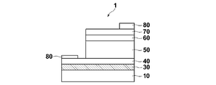
- FIG. 1 is a schematic cross-sectional view showing an embodiment of a photoelectric conversion element.
- the photoelectric conversion element 1 includes an anodic oxide film 20 formed by anodic oxidation, an alkali metal silicate layer 30, a molybdenum electrode 40, and holes / holes by light absorption.
- a photoelectric conversion semiconductor layer 50 that generates electron pairs, a buffer layer 60, a translucent conductive layer (transparent electrode) 70, and an upper electrode (grid electrode) 80 are sequentially stacked.
- 1 shows a photoelectric conversion element in which an anodized film 20 formed by anodization and an alkali metal silicate layer 30 are formed on a substrate 10, but as shown in FIG. An embodiment in which an alkali metal silicate layer 30 is formed on the substrate 10 may be used (in FIG. 2, components equivalent to those in FIG. 1 are given the same numbers). .
- a ceramic substrate such as non-alkali glass, quartz glass, or alumina
- a metal substrate such as stainless steel, titanium foil, or silicon
- a polymer substrate such as polyimide
- a metal substrate is particularly preferable.
- a material in which a metal oxide film generated on the surface of a metal substrate by anodic oxidation becomes an insulator can be used.
- a substrate containing one metal or an alloy of the above metals is preferred.
- a clad material in which one or both surfaces of aluminum, stainless steel, or steel plate are integrated with an aluminum plate is more preferable from the viewpoint of easy formation of anodization and high durability.
- an integrated clad material with both surfaces sandwiched between aluminum plates it is possible to suppress substrate warpage due to the difference in thermal expansion coefficient between aluminum and the oxide film (Al 2 O 3 ), and film peeling due to this. Therefore, it is more preferable.
- cleaning treatment / polishing smoothing treatment if necessary, for example, a degreasing step for removing the adhering rolling oil, a desmut treatment step for dissolving the smut on the surface of the aluminum plate, and roughening the surface of the aluminum plate It is preferable to use one subjected to a roughening treatment step.
- the anodic oxide film 20 formed by anodic oxidation is obtained by forming an insulating oxide film having a plurality of pores by anodic oxidation, thereby ensuring high insulation.
- Anodization can be performed by immersing the substrate 10 as an anode in an electrolyte together with a cathode, and applying a voltage between the anode and the cathode. Carbon, aluminum, or the like is used as the cathode.
- the anodizing conditions are not particularly limited depending on the type of electrolyte used.
- the conditions are, for example, an electrolyte concentration of 0.1 to 2 mol / L, a liquid temperature of 5 to 80 ° C., a current density of 0.005 to 0.60 A / cm 2 , a voltage of 1 to 200 V, and an electrolysis time of 3 to 500 minutes. Is appropriate.
- the electrolyte is not particularly limited, and an acidic electrolytic solution containing one or more acids such as sulfuric acid, phosphoric acid, chromic acid, oxalic acid, malonic acid, sulfamic acid, benzenesulfonic acid, and amidosulfonic acid is preferable. Used.
- an electrolyte concentration of 0.2 to 1 mol / L, a liquid temperature of 10 to 80 ° C., a current density of 0.05 to 0.30 A / cm 2 , and a voltage of 30 to 150 V are preferable.
- the anodic oxide film is preferably composed of a barrier layer portion and a porous layer portion, and the porous layer portion has a compressive strain at room temperature.
- the barrier layer has compressive stress and the porous layer has tensile stress, it is known that the whole anodic oxide film becomes tensile stress in a thick film of several ⁇ m or more.
- a porous layer having a compressive stress can be produced.
- the entire anodic oxide film can be subjected to compressive stress, no cracking occurs due to the difference in thermal expansion during film formation, and long-term reliability near room temperature is excellent. Insulating film can be obtained.
- the magnitude of the compressive strain is preferably 0.01% or more, more preferably 0.05% or more, and particularly preferably 0.10% or more. Moreover, it is preferable that it is 0.25% or less.
- the compressive strain is less than 0.01%, although it is compressive strain, it is insufficient and the effect of crack resistance cannot be obtained. Therefore, when the final product is subjected to bending strain, undergoes a temperature cycle over a long period of time, or receives impact or stress from the outside, cracks occur in the anodized film formed as an insulating layer, resulting in insulating properties. Leading to a decline.
- the compressive strain is preferably 0.25% or less.
- the Young's modulus of the anodic oxide film is known to be about 50 to 150 GPa. Therefore, the magnitude of the compressive stress is preferably about 5 to 300 MPa.
- the heat treatment may be performed after the anodizing treatment.
- compressive stress is applied to the anodized film, and crack resistance is increased. Therefore, heat resistance and insulation reliability are improved, and the metal substrate with an insulating layer can be more suitably used.
- the heat treatment temperature is preferably 150 ° C. or higher. When the above clad material is used, heat treatment at 300 ° C. or higher is preferable. By performing the heat treatment in advance, the amount of water contained in the porous anodic oxide film can be reduced, and the insulation can be improved.
- An anodized film is an oxide film formed in an aqueous solution, and it is described in, for example, “Chemistry Letters Vol. 34, No. 9, (2005) p1286” that moisture is retained inside a solid.
- aqueous solution As known. From the solid-state NMR measurement of the anodic oxide film as in this document, it was found that the amount of water (OH group) inside the solid of the anodic oxide film decreased when heat-treated at 100 ° C. or higher, particularly at 200 ° C. or higher is there. Therefore, it is presumed that the combined state of Al—O and Al—OH changes due to heating and stress relaxation (annealing effect) occurs.
- the anodic oxide film preferably has a thickness of 3 to 50 ⁇ m.
- a film thickness of 3 ⁇ m or more it is possible to achieve both insulation, heat resistance during film formation by having compressive stress at room temperature, and long-term reliability.
- the film thickness is preferably 5 ⁇ m or more and 30 ⁇ m or less, and particularly preferably 5 ⁇ m or more and 20 ⁇ m or less.
- the film thickness is extremely thin, there is a possibility that damage due to mechanical impact during handling and electrical insulation cannot be prevented. In addition, the insulation and heat resistance are drastically reduced, and the deterioration with time increases. This is because the influence of the unevenness on the surface of the anodized film becomes relatively large due to the thin film thickness, the crack becomes the starting point of cracks, and the anodization derived from metal impurities contained in aluminum. The effect of metal precipitates, intermetallic compounds, metal oxides, and voids in the film is relatively large, resulting in a decrease in insulation, and breakage when the anodized film is subjected to external impact or stress. This is because cracks are likely to occur. As a result, when the anodic oxide film is less than 3 ⁇ m, the insulating property is lowered, so that it is not suitable for use as a flexible heat-resistant substrate or roll-to-roll production.
- the cause of the decrease in bending resistance is that when the anodized film is bent, the tensile stress at the interface between the surface and the aluminum differs, so the stress distribution in the cross-sectional direction increases and local stress concentration occurs. This is presumed to be easier.
- the cause of the decrease in thermal strain resistance is that when a tensile stress is applied to the anodized film due to the thermal expansion of the base material, a greater stress is applied to the interface with aluminum, and the stress distribution in the cross-sectional direction increases, resulting in local stress.
- the film thickness of the molybdenum electrode 40 is not limited and is preferably about 200 to 1000 nm.
- the photoelectric conversion semiconductor layer 50 is a compound semiconductor-based photoelectric conversion semiconductor layer, and is not particularly limited as a main component (the main component means a component of 20% by mass or more), and high photoelectric conversion efficiency is obtained.
- the main component means a component of 20% by mass or more
- a compound semiconductor, a compound semiconductor having a chalcopyrite structure, or a compound semiconductor having a defect stannite structure can be preferably used.
- I-III-VI Group 2 compounds CuInSe 2 , CuGaSe 2 , Cu (In, Ga) Se 2 , CuInS 2 , CuGaSe 2 , Cu (In, Ga) (S, Se) 2, etc.
- I-III 3 -VI 5 group compounds Culn 3 Se 5 , CuGa 3 Se 5 , Cu (ln, Ga) 3 Se 5 and the like.
- I-III-VI Group 2 compounds CuInSe 2 , CuGaSe 2 , Cu (In, Ga) Se 2 , CuInS 2 , CuGaSe 2 , Cu (In, Ga) (S Se) 2, etc.
- I-III 3 -VI 5 group compounds CuIn 3 Se 5 , CuGa 3 Se 5 , Cu (In, Ga) 3 Se 5 and the like can be preferably mentioned.
- the method for forming the photoelectric conversion semiconductor layer is not particularly limited.
- a CI (G) S-based photoelectric conversion semiconductor layer containing Cu, In, (Ga), and S can be formed using a method such as a selenization method or a multi-source evaporation method.
- the film thickness of the photoelectric conversion semiconductor layer 50 is not particularly limited, and is preferably 1.0 to 3.0 ⁇ m, particularly preferably 1.5 to 2.0 ⁇ m.
- the buffer layer 60 is not particularly limited, but CdS, ZnS, Zn (S, O) and / or Zn (S, O, OH), SnS, Sn (S, O) and / or Sn (S, O, OH).
- the thickness of the buffer layer 40 is preferably 10 nm to 2 ⁇ m, and more preferably 15 to 200 nm.
- the translucent conductive layer (transparent electrode) 70 is a layer that captures light and functions as an electrode that is paired with the lower electrode 40 and through which the current generated in the photoelectric conversion layer 50 flows.
- the composition of the translucent conductive layer 70 is not particularly limited, and n-ZnO such as ZnO: Al is preferable.
- the film thickness of the translucent conductive layer 70 is not particularly limited, and is preferably 50 nm to 2 ⁇ m.
- the upper electrode (grid electrode) 80 is not particularly limited, and examples thereof include Al.
- the thickness of the upper electrode 80 is not particularly limited and is preferably 0.1 to 3 ⁇ m.
- the photoelectric conversion element of the present invention is a compound semiconductor having at least one chalcopyrite structure in which the main component of the photoelectric conversion semiconductor layer is composed of an Ib group element, an IIIb group element, and a VIb group element.
- the photoelectric conversion semiconductor layer contains lithium ions or potassium ions and sodium ions. Lithium ions and potassium ions may contain both.
- Each content of lithium ion, potassium ion and sodium ion contained in the photoelectric conversion semiconductor layer is preferably 1 ⁇ 10 15 atms / cm 3 or more. More preferably, the content of sodium ions is 1 ⁇ 10 18 atms / cm 3 ⁇ 1 ⁇ 10 20 atms / cm 3, more preferably 2 ⁇ 10 18 atms / cm 3 ⁇ 1 ⁇ 10 20 atms / cm 3, further Is preferably 5 ⁇ 10 18 atoms / cm 3 to 1 ⁇ 10 20 atoms / cm 3 .
- the lithium ion or potassium ion content is 1 ⁇ 10 15 atms / cm 3 to 5 ⁇ 10 19 atms / cm 3 , more preferably 1 ⁇ 10 16 atms / cm 3 to 5 ⁇ 10 19 atms / cm 3 , 1 ⁇ 10 17 atoms / cm 3 to 5 ⁇ 10 19 atoms / cm 3 are preferable.
- Lithium ions or potassium ions and sodium ions contained in the photoelectric conversion semiconductor layer may be co-evaporated at the time of film formation of the photoelectric conversion semiconductor layer, or fluoride such as NaF, LiF, KF, etc. on the Mo electrode in advance. It may be evaporated.
- a photoelectric conversion semiconductor layer is formed on a Mo film containing Na, Li, or K, or a compound containing Na, Li, or K is deposited and post-annealed after the photoelectric conversion semiconductor layer is formed. Good.
- the photoelectric conversion element substrate with a molybdenum electrode according to the first aspect and the photoelectric conversion element substrate with a molybdenum electrode according to the second aspect may be used to transmit and diffuse the molybdenum electrode 40 from the alkali supply layer 30.
- the photoelectric conversion element substrate of the present invention can be preferably used for solar cells and the like. If necessary, a cover glass, a protective film, or the like can be attached to the photoelectric conversion element 1 to form a solar cell.
- a cover glass, a protective film, or the like can be attached to the photoelectric conversion element 1 to form a solar cell.
- the substrate for photoelectric conversion element of the present invention will be described in more detail with reference to examples.
- Lithium supply source (manufactured by Nissan Chemical, trade names: lithium silicate 45, lithium silicate 75, lithium hydroxide), potassium supply source (manufactured by Fuji Chemical, trade names: 1K potassium silicate, 2K potassium silicate), sodium supply source ( Showa Chemical Co., Ltd., trade name: No. 1 sodium silicate, No. 3 sodium silicate, and Toso Sangyo, trade name: No. 4 sodium silicate, high-mol sodium silicate, sodium hydroxide) and water are shown in Table 1.
- boron or sodium tetraborate as a boron supply source and phosphoric acid as a phosphoric acid source were added at a mass ratio shown in Table 2 to prepare a coating solution.
- the coating solution was dropped on the substrate, and an alkali metal silicate layer was formed by spin coating. Thereafter, the substrate was heat-treated at 450 ° C. for 30 minutes. After the heat treatment, Mo was formed to a thickness of 800 nm on the substrate by DC sputtering.
- Example 9 The amount of impurities on the Mo surface on the alkali metal silicate layer formed above was observed using an optical microscope to observe the amount of foreign matter.
- the micrographs of Example 9 and Comparative Example 1 are shown in FIG. In Example 9, no foreign matter was observed, but in Comparative Example 1, 10,000 or more foreign matters were observed per 1 mm square. Other examples and comparative examples were similarly observed with a microscope, and evaluated according to the following criteria according to the number of foreign matters per 1 mm square, and are shown in Tables 1 to 3.
- AA no foreign matter was observed
- A 1 to 10 foreign matters
- B 10 to less than 100 foreign matters
- C 10000 foreign matters
- a CIGS solar cell was formed on the Mo electrode.
- granular raw materials of high-purity copper and indium (purity 99.9999%), high-purity Ga (purity 99.999%), and high-purity Se (purity 99.999%) were used as the evaporation source.
- a chromel-alumel thermocouple was used as a substrate temperature monitor. After the main vacuum chamber is evacuated to 10 ⁇ 6 Torr (1.3 ⁇ 10 ⁇ 3 Pa), the deposition rate from each evaporation source is controlled, and the film thickness is about 530 ° C. under the film forming conditions. A 1.8 ⁇ m CIGS thin film was formed.
- a CdS thin film of about 90 nm was deposited as a buffer layer by a solution growth method, and a ZnO: A1 film of a transparent conductive film was formed thereon with a thickness of 0.6 ⁇ m by a DC sputtering method.
- an Al grid electrode was formed as an upper electrode by a vapor deposition method to produce a solar battery cell.
- AM Air Mass
- the photoelectric conversion efficiency was measured under the above conditions, and the maximum value among them was defined as the conversion efficiency of the photoelectric conversion element of each example and comparative example.
- the coefficient of variation (a value obtained by dividing the standard deviation of 8 cells by the average value) was evaluated as a variation in cell efficiency.
- the sodium concentration of the photoelectric converting layer was measured. This sodium concentration was measured using SIMS (secondary ion mass spectrometer). Primary ion species for measurement and Cs +, the acceleration voltage was set to 5.0 kV. Although the sodium concentration in the photoelectric conversion layer (CIGS layer) has a distribution in the thickness direction, it was integrated to derive an average value, and this average value was used for evaluation of the sodium concentration.
- Tables 1, 2 and 3 show the results of measurement of Mo film suitability, sodium concentration, and power generation efficiency together with the formulation of the coating solution.
- the mass ratio of the sodium source, lithium source and potassium source used in the examples and comparative examples Tables 4, 5 and 6 show.
- the molar ratios in Tables 1, 2 and 3 are converted from this mass ratio to molar ratio (so that sodium hydroxide and lithium hydroxide are solid).
- the sum of the molar ratio in Table 1 is a value calculated before rounding off the three decimal places of the molar ratio of lithium or potassium to silicon and the molar ratio of sodium to silicon.
- Examples 1 to 10 in which an alkali metal silicate layer containing lithium silicate or potassium silicate and sodium silicate was provided are alkali metal silicate layers made only of sodium silicate.
- the power generation efficiency was nearly double. In any of these cases, the sodium concentration is almost the same level, and it is considered that the sodium is sufficiently diffused into CIGS.
- Mo in Comparative Examples 5 to 8 has a high impurity peak ratio, which is attributed to this. It is thought that the power generation efficiency was low.
- Comparative Examples 1 and 2 which are alkali metal silicate layers made only of lithium silicate
- Comparative Examples 3 and 4 which are alkali metal silicate layers made only of potassium silicate
- the film forming suitability of Mo was good.
- the power generation efficiency was about 30% lower than that of the example on average. Since sodium is not present in the alkali metal silicate layer, it is considered that sodium was not diffused into CIGS and the efficiency was not improved. This shows that the power generation efficiency can be greatly increased by using lithium silicate or potassium silicate in combination with sodium silicate.
- Example 11 uses sodium hydroxide as a sodium supply source in place of sodium silicate and uses lithium silicate in combination.
- lithium hydroxide was used as a lithium supply source instead of lithium silicate, and sodium silicate was used in combination. Even in this case, the obtained alkali metal silicate is a mixture of sodium silicate and lithium silicate according to the present invention.
- film forming suitability and power generation efficiency were slightly low. This is presumably because the sum of the molar ratio of lithium to silicon and the molar ratio of sodium to silicon is greater than one.
- Example 13 was slightly inferior in power generation efficiency. This is considered because the molar ratio of lithium to silicon is larger than 1.
- FIG. 2 is an electron micrograph of CIGS crystals of Example 4 and Comparative Examples 1 and 5.
- Example 4 which is the substrate for photoelectric conversion elements of the present invention
- the grain size of the CIGS crystal is larger than that of Comparative Example 1, and the effect of adding an alkali is confirmed. It was.
- Comparative Example 5 also has a large particle size and an alkali addition effect, but the conversion efficiency is low because the suitability of Mo film formation is low and impurities are formed at the Mo / CIGS interface.
- the addition amount of the sodium source, the lithium source, and the potassium source was changed. From these examples, the molar ratio of lithium or potassium to silicon is in the range of 1 or less, and the sum of the molar ratio of lithium to silicon and the molar ratio of sodium to silicon is also 1 or less.
- the alkali metal silicate layer further contains boron or phosphorus. At first glance, it seems that there is no significant difference in power generation efficiency as compared with Examples not containing boron or phosphorus. As can be seen, since the coefficient of variation is small, all of the fabricated cells have high power generation efficiency, and it can be seen that the power generation efficiency of the entire fabricated cell is increased.
- a substrate As a substrate, a 3 cm square glass substrate, a SUS430 substrate (thickness: 100 ⁇ m), and an anodized aluminum substrate were prepared.
- the anodized aluminum substrate was produced by the following method. Each of a clad material made of 30 ⁇ m thick aluminum and 50 ⁇ m thick SUS430 is anodized under a constant voltage condition of 40 V using an oxalic acid electrolytic solution to produce a substrate on which 10 ⁇ m anodized aluminum is formed. did.
- the mixture was mixed to prepare a coating solution.
- the coating solution was dropped on the substrate, and an alkali metal silicate layer was formed by spin coating. Thereafter, the substrate was heat-treated at 450 ° C. for 30 minutes. After the heat treatment, Mo was formed to a thickness of 800 nm on the substrate by DC sputtering. In Comparative Example 3, the coating solution was solidified and could not be applied.
- Example 9 The amount of impurities on the Mo surface on the alkali metal silicate layer formed above was observed using an optical microscope to observe the amount of foreign matter.
- the micrographs of Example 9 and Comparative Example 1 are shown in FIG.
- Example 9 no foreign matter was observed, but in Comparative Example 1, 10,000 or more foreign matters were observed per 1 mm square.
- Other examples and comparative examples were similarly observed with a microscope, and evaluated according to the following criteria according to the number of foreign matters per 1 mm square, and are shown in Tables 1 and 2.
- AA no foreign matter was observed
- A 1 to 10 foreign matters
- B 10 to less than 100 foreign matters
- C 10000 foreign matters
- a CIGS solar cell was formed on the Mo electrode.
- granular raw materials of high-purity copper and indium (purity 99.9999%), high-purity Ga (purity 99.999%), and high-purity Se (purity 99.999%) were used as the evaporation source.
- a chromel-alumel thermocouple was used as a substrate temperature monitor. After the main vacuum chamber is evacuated to 10 ⁇ 6 Torr (1.3 ⁇ 10 ⁇ 3 Pa), the deposition rate from each evaporation source is controlled, and the film thickness is about 530 ° C. under the film forming conditions. A 1.8 ⁇ m CIGS thin film was formed.
- a CdS thin film of about 90 nm was deposited as a buffer layer by a solution growth method, and a ZnO: A1 film of a transparent conductive film was formed thereon with a thickness of 0.6 ⁇ m by a DC sputtering method.
- an Al grid electrode was formed as an upper electrode by a vapor deposition method to produce a solar battery cell.
- Eight samples were produced for each of the solar cells of Examples and Comparative Examples.
- the photoelectric conversion efficiency was measured under the above conditions, and the highest value and the coefficient of variation (the value obtained by dividing the standard deviation of 8 cells by the average value) in each example and comparative example solar cell. was evaluated as the conversion efficiency and variation.
- Tables 7 and 8 show the measurement results of the number of foreign matters and the power generation efficiency as Mo surface property evaluation together with the formulation of the coating solution.
- the molar ratios in Tables 7 and 8 are converted from the mass ratio to the molar ratio.
- Examples 10 to 16 the surface properties of Mo were further improved compared to Examples 1 to 5, and the power generation efficiency was high, and the variation was further reduced. This shows that the power generation efficiency can be further increased by using lithium silicate or potassium silicate in combination with sodium silicate.
- Examples 6 to 9 were obtained by reducing the molar ratio of boron or phosphorus in Example 4, and Examples 17 to 20 were obtained by reducing the molar ratio of boron or phosphorus in Example 11 or 13. From the comparison, it can be seen that the molar ratio of silicon to 0.002 or more is more preferable in order to reduce foreign substances.
Abstract
【課題】光電変換素子用基板を、アルカリ金属イオンを光電変換半導体層に対して効率よく拡散することが可能であって、光電変換素子の光電変換効率を高くすることができるものとする。 【解決手段】光電変換素子用基板を、基板(10)上にケイ酸リチウムまたはケイ酸カリウムと、ケイ酸ナトリウムとを含むアルカリ金属ケイ酸塩層(30)を有するものとする。あるいは、基板(10)上に、アルミニウムを除く13族元素または窒素を除く15族元素のうち少なくとも1種と、ケイ素と、アルカリ金属を含み、液相法によって形成されたアルカリ金属ケイ酸塩層(但し、アルカリ土類金属を含まない)(30)を有するものとする。
Description
本発明は、モリブデン電極付光電変換素子用基板および太陽電池等の用途に好適な光電変換素子、並びに太陽電池に関するものである。
下部電極(裏面電極)と光吸収により電流を発生する光電変換層と上部電極(透明電極)との積層構造を基板上に有する光電変換素子が、太陽電池等の用途に使用されている。従来、太陽電池においては、バルクの単結晶Si又は多結晶Si、あるいは薄膜のアモルファスSiを用いたSi系太陽電池が主流であったが、近年Siに依存しない化合物半導体系太陽電池の研究開発がなされている。化合物半導体系太陽電池として、Ib族元素とIIIb族元素とVIb族元素とからなるCIS(Cu-In-Se)系あるいはCIGS(Cu-In-Ga-Se)系等の薄膜系が光吸収率が高く、光電変換効率が高いことが知られている。
CIS系あるいはCIGS系等の光電変換素子においては、アルカリ金属、好ましくはNaを光電変換層に拡散させることで、光電変換層の結晶性が良くなり、光電変換効率が向上することが知られている(特許文献1および2)。従来は、Naを含むソーダライムガラス基板を用いて、光電変換層にNaを拡散させることがなされている。
しかしながら、金属基板、高分子基板、セラミックス基板などを太陽電池基板として用いた場合には、基板からナトリウムを供給することができないため、変換効率が上がらないという問題がある。そこで、ナトリウムを含まない基板を用いる場合には、アルカリ供給層を液相法で設けたり、ナトリウムをCIGSとの共蒸着で導入したり、あるいは電極としてMo-Naを設けること等が行われている。例えば、特許文献3には液相塗布により、アルカリ金属ケイ酸塩、詳細にはナトリウムケイ酸塩を塗布することが開示されている。また、特許文献4には陽極酸化基板を水酸化ナトリウム水溶液と接触させ、ナトリウムをドープすることが開示されている。さらに特許文献5にはステンレス基板にゾルゲル法で酸化ケイ素膜を形成するとともに、さらにNaを含む材料で絶縁層を形成することが記載されている。
ところで、ナトリウム以外のアルカリ金属であるリチウムやカリウム、セシウムは、ナトリウムに比べて、CIGSへ添加できる量が少なく、また、添加しても光電変換効率向上の効果が低いことが知られている(非特許文献1および2)。
ThinSolid Films, 第361巻, p.9-p.16 (2000)
M. A. contreras, et. al著,「ConferenceRecord of the Twenty Sixth IEEE Photovoltaic Specialists Conference」,2000年,p.359-p.362,表題「Onthe role of Na and modifications to CIGS absorber materials using high MFprecursor layers」
上記のように、従来、光電変換半導体層を形成する際に、ナトリウム供給層からナトリウムが光電変換半導体層に拡散することによって発電効率が向上するという知見がごく一般的なものであったが、ナトリウム供給層を設けても想定している以上には発電効率が高くならないことがわかった。その原因は、ナトリウムが電極のモリブデンと反応するために不純物が生成していること、集積化された太陽電池の製造工程では電極成膜後のスクライブ実施後に、水洗を行う必要が出てくるが、この水洗によってナトリウムが溶出し、ロスにつながっていることが判明した。なお、ナトリウムとモリブデンの反応は、スパッタエネルギーが反応の駆動力と推定され、主に、アルカリ金属ケイ酸塩層上にモリブデンをスパッタする際に起こる。
本発明は上記事情に鑑みなされたものであり、アルカリ金属イオンを光電変換半導体層に対して効率よく拡散することが可能であって、光電変換素子の光電変換効率を高くすることができる光電変換素子用基板、並びに光電変換素子、さらには太陽電池を提供することを目的とするものである。
本発明の第一の態様のモリブデン電極付光電変換素子用基板は、基板上に、ケイ酸リチウムまたはケイ酸カリウムと、ケイ酸ナトリウムとを含むアルカリ金属ケイ酸塩層が積層された光電変換素子用基板と、アルカリ金属ケイ酸塩層上に積層されたモリブデン電極とからなることを特徴とするものである。
第一の態様におけるアルカリ金属ケイ酸塩層のケイ素に対するリチウムまたはカリウムのモル比は0.001以上1以下であることが好ましい。
第一の態様におけるケイ素に対するリチウムまたはカリウムのモル比と、ケイ素に対するナトリウムのモル比との和は1以下であることが好ましい。
第一の態様におけるアルカリ金属ケイ酸塩層はホウ素またはリンを含むことが好ましい。
第一の態様におけるアルカリ金属ケイ酸塩層のケイ素に対するリチウムまたはカリウムのモル比は0.001以上1以下であることが好ましい。
第一の態様におけるケイ素に対するリチウムまたはカリウムのモル比と、ケイ素に対するナトリウムのモル比との和は1以下であることが好ましい。
第一の態様におけるアルカリ金属ケイ酸塩層はホウ素またはリンを含むことが好ましい。
第一の態様におけるアルカリ金属ケイ酸塩層の厚さは2μm以下であることが好ましい。
第一の態様における基板は金属基板であることが好ましい。
金属基板の表面に陽極酸化アルミニウム皮膜が形成されていることが好ましい。
金属基板はアルミニウム、ステンレスまたは鉄鋼板の片面あるいは両面をアルミニウム板で一体化したクラッド材であることが好ましい。
陽極酸化アルミニウム皮膜はポーラス型陽極酸化アルミニウム皮膜であって、該ポーラス型陽極酸化アルミニウム皮膜が圧縮応力を有することが好ましい。
本発明の光電変換素子は、上記第一の態様の光電変換素子用基板上に形成されたものとすることができる。
第一の態様における基板は金属基板であることが好ましい。
金属基板の表面に陽極酸化アルミニウム皮膜が形成されていることが好ましい。
金属基板はアルミニウム、ステンレスまたは鉄鋼板の片面あるいは両面をアルミニウム板で一体化したクラッド材であることが好ましい。
陽極酸化アルミニウム皮膜はポーラス型陽極酸化アルミニウム皮膜であって、該ポーラス型陽極酸化アルミニウム皮膜が圧縮応力を有することが好ましい。
本発明の光電変換素子は、上記第一の態様の光電変換素子用基板上に形成されたものとすることができる。
本発明の第二の態様の光電変換素子用基板は、基板上に、アルミニウムを除く13族元素または窒素を除く15族元素のうち少なくとも1種と、ケイ素と、アルカリ金属を含み、液相法によって形成されたアルカリ金属ケイ酸塩層(但し、アルカリ土類金属を含まない)を有し、このアルカリ金属ケイ酸塩層上に積層されたモリブデン電極とからなることを特徴とするものである。
アルミニウムを除く13族元素または窒素を除く15族元素はホウ素またはリンであることが好ましい。
アルミニウムを除く13族元素または窒素を除く15族元素はホウ素またはリンであることが好ましい。
第二の態様におけるアルカリ金属はナトリウムであることが好ましい。
第二の態様におけるアルカリ金属はリチウムまたはカリウムと、ナトリウムとの2種を含むことがより好ましい。
ケイ素に対する、前記アルミニウムを除く13族元素または窒素を除く15族元素の合計のモル比は0.15以下であることがより好ましい。
第二の態様におけるアルカリ金属はリチウムまたはカリウムと、ナトリウムとの2種を含むことがより好ましい。
ケイ素に対する、前記アルミニウムを除く13族元素または窒素を除く15族元素の合計のモル比は0.15以下であることがより好ましい。
第二の態様におけるアルカリ金属ケイ酸塩層の厚さは2μm以下であることが好ましい。
第二の態様における基板は金属基板であることがより好ましい。
金属基板の表面に陽極酸化アルミニウム皮膜を形成したものであることがさらに好ましい。
金属基板はアルミニウム、ステンレスまたは鉄鋼板の片面あるいは両面をアルミニウム板で一体化したクラッド材であることがより好ましい。
本発明の光電変換素子は、上記第二の態様の光電変換素子用基板上に形成されたものとすることができる。
第二の態様における基板は金属基板であることがより好ましい。
金属基板の表面に陽極酸化アルミニウム皮膜を形成したものであることがさらに好ましい。
金属基板はアルミニウム、ステンレスまたは鉄鋼板の片面あるいは両面をアルミニウム板で一体化したクラッド材であることがより好ましい。
本発明の光電変換素子は、上記第二の態様の光電変換素子用基板上に形成されたものとすることができる。
本発明の光電変換素子は、別の側面からすれば、基板上にモリブデン電極と光電変換半導体層と上部電極とが順次積層された光電変換素子であって、光電変換半導体層の主成分がIb族元素とIIIb族元素とVIb族元素とからなる少なくとも1種のカルコパイライト構造の化合物半導体であり、光電変換半導体層中に、リチウムイオンまたはカリウムイオンと、ナトリウムイオンとを含むことを特徴とするものである。
光電変換半導体層中に含まれるリチウムイオンまたはカリウムイオンと、ナトリウムイオンのそれぞれの含有量は1×10¹⁵atms/cm3以上であることが好ましい。
光電変換半導体層中に含まれるリチウムイオンまたはカリウムイオンと、ナトリウムイオンのそれぞれの含有量は1×10¹⁵atms/cm3以上であることが好ましい。
光電変換半導体層中に含まれるリチウムイオンまたはカリウムイオンと、ナトリウムイオンは、基板とモリブデン電極との間に形成されたアルカリ供給層から供給されたものであることが好ましい。
光電変換半導体層の主成分は、Cu及びAgからなる群より選択された少なくとも1種のIb族元素と、Al,Ga及びInからなる群より選択された少なくとも1種のIIIb族元素と、S,Se,及びTeからなる群から選択された少なくとも1種のVIb族元素とからなる少なくとも1種の化合物半導体であることが好ましい。
光電変換半導体層の主成分は、Cu及びAgからなる群より選択された少なくとも1種のIb族元素と、Al,Ga及びInからなる群より選択された少なくとも1種のIIIb族元素と、S,Se,及びTeからなる群から選択された少なくとも1種のVIb族元素とからなる少なくとも1種の化合物半導体であることが好ましい。
上記基板は金属基板であることが好ましい。
金属基板の表面に陽極酸化アルミニウム皮膜が形成されていることが好ましい。
金属基板はアルミニウム、ステンレスまたは鉄鋼板の片面あるいは両面をアルミニウム板で一体化したクラッド材であることが好ましい。
陽極酸化アルミニウム皮膜はポーラス型陽極酸化アルミニウム皮膜であって、ポーラス型陽極酸化アルミニウム皮膜が圧縮応力を有することが好ましい。
本発明の太陽電池は、上記の光電変換素子を備えたものとすることができる。
金属基板の表面に陽極酸化アルミニウム皮膜が形成されていることが好ましい。
金属基板はアルミニウム、ステンレスまたは鉄鋼板の片面あるいは両面をアルミニウム板で一体化したクラッド材であることが好ましい。
陽極酸化アルミニウム皮膜はポーラス型陽極酸化アルミニウム皮膜であって、ポーラス型陽極酸化アルミニウム皮膜が圧縮応力を有することが好ましい。
本発明の太陽電池は、上記の光電変換素子を備えたものとすることができる。
本発明の第一の態様の光電変換素子用基板は、アルカリ金属ケイ酸塩(但し、アルカリ金属はナトリウム以外)と、ケイ酸ナトリウムとを含むアルカリ金属ケイ酸塩層を有し、ナトリウムと別のアルカリ金属を併用することによって、アルカリ金属ケイ酸塩層上にモリブデンからなる電極を形成しても、ナトリウムとモリブデンとが反応して不純物が生成したり、水洗によってナトリウムが溶出したりすることが抑制されるので、アルカリ金属ケイ酸塩層のナトリウムを効率よく光電変換半導体層に拡散することができ、光電変換素子の発電効率を向上させることが可能である。
ナトリウムと別のアルカリ金属を併用することによって、このような効果が得られるその作用機序は必ずしも明らかではないが、ナトリウムに比べると別のアルカリ金属、とりわけリチウムやカリウムは吸湿性が低く、アルカリ金属ケイ酸塩層にリチウムやカリウムが含まれることによって、アルカリ金属ケイ酸塩層の含まれる水分が絶対的に減る結果、水分に起因して生じる酸化反応が起こりにくくなるために、不純物の生成が抑制され、また、水洗によるナトリウム溶出が軽減されるものと推測される。
本発明の第二の態様の光電変換素子用基板は、アルカリ金属ケイ酸塩層にアルミニウムを除く13族元素または窒素を除く15族元素のうち少なくとも1種を含むので、アルカリ金属ケイ酸塩層上にモリブデンからなる電極を形成しても、ナトリウムとモリブデンとが反応して異物が生成されたり、水洗によってアルカリ金属が溶出したりすることが抑制されるので、アルカリ金属ケイ酸塩層のアルカリ金属を効率よく光電変換半導体層に拡散することができ、光電変換素子の発電効率を向上させることが可能である。
アルカリ金属ケイ酸塩層がアルミニウムを除く13族元素または窒素を除く15族元素のうち少なくとも1種を含有することによって、このような効果が得られるその作用機序は必ずしも明らかではないが、次のようなメカニズムが推定される。ケイ素、アルカリ金属および酸素だけからなるアルカリ金属ケイ酸塩層の場合、アルカリ金属イオンはガラス中に固溶しているが、アルカリ金属イオンは1価であるため、ケイ素-酸素からなるガラスネットワークを形成しない。このため、アルカリ金属は酸素との相互作用が不充分で、ガラス中から遊離し、表面に偏析しやすい。アルカリ金属イオンが表面に偏析すると、電極を設ける際の、高いエネルギーを有するスパッタモリブデンと反応し、異物が生成するという問題が発生する。
一方、アルミニウムを除く13族元素または窒素を除く15族元素の酸化物は、ケイ酸ガラス中に固溶し、単一相のガラスを形成することが知られているが、本発明のアルカリ金属ケイ酸塩層においても、アルミニウムを除く13族元素または窒素を除く15族元素を添加することにより、これらの元素のイオンはケイ素-酸素からなるガラスネットワークに取り込まれて均一なガラスを形成する。詳細は必ずしも明らかではないが、ガラスのミクロな構造が変化し、ガラス中でのアルカリ金属イオンの安定性が向上したために、アルカリ金属イオンの遊離が抑制され、アルカリ金属イオンの表面への偏析が起こらず、モリブデンスパッタに際する異物の生成が防止できるものと推定される。また、アルカリ金属イオンの表面への偏析が抑制されるために、水洗によるアルカリ金属イオン溶出も軽減されるものと推測される。
本発明の光電変換素子は光電変換半導体層中にナトリウムイオン以外に、リチウムイオンまたはカリウムイオンを含むことによって、光電変換素子の発電効率を向上させることが可能である。ナトリウムイオンにリチウムイオンまたはカリウムイオンを組み合わせることによって特性が向上する作用機序は必ずしも明らかではない。しかし、光電変換半導体層中の元素分析によれば、ナトリウムイオンに加えてリチウムイオンまたはカリウムイオンを含む光電変換半導体層と、ナトリウムイオンのみを含む光電変換半導体層では、光電変換半導体層中に含まれるナトリウムの量はほぼ同等である。このことから、光電変換半導体層の物性、特性に与える影響は明確ではないものの、リチウムイオンまたはカリウムイオンの存在が光電変換効率の向上に寄与していることが推測される。このことは本発明者によって初めて見出されたものである。
本発明の第一の態様の光電変換素子用基板について詳細に説明する。
第一の態様の光電変換素子用基板におけるアルカリ金属ケイ酸塩層は、ケイ酸リチウムまたはケイ酸カリウムと、ケイ酸ナトリウムとを含むものである。ケイ酸リチウムとケイ酸カリウムはその両方を含むものであってもよい。
第一の態様の光電変換素子用基板におけるアルカリ金属ケイ酸塩層は、ケイ酸リチウムまたはケイ酸カリウムと、ケイ酸ナトリウムとを含むものである。ケイ酸リチウムとケイ酸カリウムはその両方を含むものであってもよい。
アルカリ金属ケイ酸塩層のケイ素に対するリチウムまたはカリウムのモル比は0.001以上1以下であることが好ましく、より好ましくは0.01以上1以下、さらに好ましくは0.02以上1以下、特に好ましくは0.05以上0.5以下が望ましい。ケイ素はアルカリ金属ケイ酸塩層に含まれる全ケイ素(ケイ酸ナトリウム由来のケイ素も含む)であり、ケイ酸リチウムとケイ酸カリウムの両方を含む場合には、ケイ酸リチウム由来、ケイ酸カリウム由来、およびケイ酸ナトリウム由来のケイ素に対するリチウムとカリウムの和のモル比を意味する。ケイ素に対するリチウムまたはカリウムのモル比が1よりも大きくなるとリチウムまたはカリウムが多くなりすぎて、ケイ酸塩として固化しにくくなる。一方で、ケイ素に対するリチウムまたはカリウムのモル比が0.001未満では、リチウムまたはカリウムが少なすぎて添加効果が得られず、光電変換素子の光電変換効率が高くならない。
アルカリ金属ケイ酸塩層に含まれる全ケイ素に対するリチウムまたはカリウムのモル比と、アルカリ金属ケイ酸塩層に含まれる全ケイ素に対するナトリウムのモル比との和は1以下であることが好ましく、より好ましくは0.8以下であることが望ましい。リチウムまたはカリウムが含まれないと絶縁性が低くなるほか、一般的に裏面電極に用いられているモリブデンを成膜した際に不純物を形成するため、発電効率が低くなる。これはナトリウムの吸水性が高いためであると推定される。一方で、リチウムまたはカリウムだけでは発電効率を上げることはできない。また、ケイ素に対するリチウムまたはカリウムのモル比と、ケイ素に対するナトリウムのモル比との和が1より大きくなると、ケイ酸塩として固化しにくく、またケイ素の量が少ないために基板との密着性が低下する。
ケイ酸ナトリウム、ケイ酸リチウム、ケイ酸カリウムの製法は、湿式法、乾式法などが知られており、酸化ケイ素を、それぞれ水酸化ナトリウム、水酸化リチウム、水酸化カリウムで溶解するなどの手法によって作製することができる。また、種々のモル比のアルカリ金属ケイ酸塩が市販されており、これを利用することもできる。
ケイ酸ナトリウム、ケイ酸リチウム、ケイ酸カリウムとしては、種々のモル比のケイ酸ナトリウム、ケイ酸リチウム、ケイ酸カリウムが市販されている。ケイ素とアルカリ金属の割合を示す指標として、SiO2/A2O(A:アルカリ金属)のモル比がしばしば用いられている。例えば、ケイ酸リチウムとしては、日産化学工業株式会社のリチウムシリケート35、リチウムシリケート45、リチウムシリケート75などがある。ケイ酸カリウムとしては、1号ケイ酸カリウム、2号ケイ酸カリウムなどが市販されている。
ケイ酸ナトリウムとしては、オルトケイ酸ナトリウム、メタケイ酸ナトリウム、1号ケイ酸ナトリウム、2号ケイ酸ナトリウム、3号ケイ酸ナトリウム、4号ケイ酸ナトリウムなどが知られ、ケイ素のモル比を数十まで高めた高モルケイ酸ナトリウムも市販されている。
上記のケイ酸ナトリウム、ケイ酸リチウム、ケイ酸カリウムを、それぞれ水と任意の比率で混合することにより、任意の濃度の溶液を得ることができる。ケイ素に対するリチウムまたはカリウムの比率は、これらのアルカリ金属ケイ酸塩の混合により変化させることができるほか、各種のケイ酸ナトリウムを任意の比率で混合することによって変化させることができる。水の添加量を変更することにより塗布液の粘度を調整し、適切な塗布条件を定めることができる。塗布液を基板上に塗布する方法としては特に限定はなく、例えば、ドクターブレード法、ワイヤーバー法、グラビア法、スプレー法、ディップコート法、スピンコート法、キャピラリーコート法等の手法を用いることができる。
なお、アルカリ金属ケイ酸塩層のケイ酸リチウム、ケイ酸カリウムおよびケイ酸ナトリウムは、作製時の供給源が必ずしもケイ酸リチウム、ケイ酸カリウムおよびケイ酸ナトリウムである必要はない。例えばアルカリ金属ケイ酸塩層がケイ酸リチウムとケイ酸ナトリウムを含む場合には、ケイ酸リチウムと水酸化ナトリウムあるいは、水酸化リチウムとケイ酸ナトリウムとを、アルカリ金属ケイ酸塩層がケイ酸カリウムとケイ酸ナトリウムを含む場合には、水酸化カリウムとケイ酸ナトリウムあるいは、ケイ酸カリウムと水酸化ナトリウムとを、それぞれ水と任意の比率で混合することによっても、ケイ酸リチウムとケイ酸ナトリウムあるいはケイ酸カリウムとケイ酸ナトリウムを含むアルカリ金属ケイ酸塩層を作製することができる。また、供給源として、それぞれ、リチウム塩、カリウム塩、ナトリウム塩を添加してもよい。例えば、硝酸塩、硫酸塩、酢酸塩、リン酸塩、塩化物、臭化物、ヨウ化物などが用いられる。
ケイ酸リチウム、ケイ酸カリウム、ケイ酸ナトリウム以外のアルカリ金属ケイ酸塩の塗布液は、所望のアルカリ金属の硝酸塩、硫酸塩、酢酸塩、リン酸塩、塩化物、臭化物、ヨウ化物などを、ケイ酸ナトリウム溶液に対して添加することによって簡便に得ることができる。
アルカリ金属ケイ酸塩水溶液に、ホウ素を含む化合物、またはリンを含む化合物を添加してもよい。これらを添加することにより、さらにMo成膜適性と発電効率を向上させることができる。詳細は必ずしも明らかではないが、ホウ素またはリンが、アルカリ金属ケイ酸塩に添加されることによって、ガラスのミクロな構造が変化し、ガラス中でのアルカリ金属イオンの安定性が向上するために、アルカリ金属イオンの遊離が抑制され、Mo成膜適性が向上し、発電効率が向上するものと推定される。
ホウ素源としては、ホウ酸、四ホウ酸ナトリウムなどのホウ酸塩が好ましく挙げられる。
リン源としては、リン酸、ペルオキソリン酸、ホスホン酸、ホスフィン酸、二リン酸、三リン酸、ポリリン酸、シクロ-三リン酸、シクロ-四リン酸、二ホスホン酸、およびこれらの塩、などがあり、例えば、リン酸リチウム、リン酸ナトリウム、リン酸カリウム、リン酸水素リチウム、リン酸アンモニウム、リン酸水素ナトリウム、リン酸水素カルシウム、リン酸水素アンモニウム、リン酸二水素リチウム、リン酸二水素ナトリウム、リン酸二水素カルシウム、リン酸二水素アンモニウム、ピロリン酸ナトリウム、三リン酸ナトリウムなどが好ましく挙げられる。
リン源としては、リン酸、ペルオキソリン酸、ホスホン酸、ホスフィン酸、二リン酸、三リン酸、ポリリン酸、シクロ-三リン酸、シクロ-四リン酸、二ホスホン酸、およびこれらの塩、などがあり、例えば、リン酸リチウム、リン酸ナトリウム、リン酸カリウム、リン酸水素リチウム、リン酸アンモニウム、リン酸水素ナトリウム、リン酸水素カルシウム、リン酸水素アンモニウム、リン酸二水素リチウム、リン酸二水素ナトリウム、リン酸二水素カルシウム、リン酸二水素アンモニウム、ピロリン酸ナトリウム、三リン酸ナトリウムなどが好ましく挙げられる。
塗布液を基板上に塗布した後、熱処理を行うことによりアルカリ金属ケイ酸塩層を作製することができる。熱重量分析、および昇温脱ガス分析の手法を用いて発明者らが脱水温度を測定したところ、脱水は200℃~300℃程度で起こることがわかった。200℃よりも低温では、塗布液を十分に乾燥させることができず、耐水性の高いアルカリ金属ケイ酸塩層が形成されないため、好ましくない。また、300℃以下の熱処理では、アルカリ金属ケイ酸塩層の残留水分が多く、大気中の二酸化炭素などと反応して表面に炭酸塩などの不純物が形成したり、Mo電極スパッタ時にモリブデン酸ナトリウムなどが生成したり、といった問題が発生する。したがって、熱処理温度は、200℃以上が好ましく、300℃以上がさらに好ましく、400℃以上が特に好ましい。
このようなより高温での熱処理を実施することから、第一の態様で用いられる基板は、アルミニウムと異種金属を複合し、アルミニウム表面に陽極酸化皮膜を形成したクラッド基板を用いることが好ましい。クラッド基板については後述するが、400℃以上の高温でも、陽極酸化皮膜のクラックなどが発生せず、高い耐熱性を有していることが知られている。また、基板をあらかじめ300℃以上で熱処理することによって陽極酸化皮膜に圧縮応力を付与することができ、さらに耐熱性を向上させ、絶縁性の長期信頼性を確保できることが知られている。この処理をアルカリ金属ケイ酸塩層の塗布後に実施することにより、アルカリ金属ケイ酸塩層の脱水に必要な熱処理と、陽極酸化皮膜の圧縮応力化に必要な熱処理を兼ねることが可能である。
一方で、600℃を超える温度では、アルカリ金属ケイ酸塩のガラス転移温度を超えるため好ましくない。
一方で、600℃を超える温度では、アルカリ金属ケイ酸塩のガラス転移温度を超えるため好ましくない。
熱処理後のアルカリ金属ケイ酸塩層の厚さは0.01~2μm、好ましくは0.05~1.5μm、さらには0.1~1μmであることが好ましい。アルカリ金属ケイ酸塩層の厚さが2μmよりも厚くなると、熱処理時のアルカリ金属ケイ酸塩の収縮量が大きくなってクラックが発生しやすくなるため、好ましくない。
次に、本発明の第二の態様の光電変換素子用基板について詳細に説明する。第二の態様の光電変換素子用基板におけるアルカリ金属ケイ酸塩層は、アルミニウムを除く13族元素または窒素を除く15族元素(以下、単に13族元素または15族元素ともいう)のうち少なくとも1種と、ケイ素と、アルカリ金属を含み、液相法によって形成されたことを特徴とする。
13族元素または15族元素は、ホウ素またはリンであることが好ましい。
また、アルカリ金属はナトリウムであることが好ましく、リチウムとナトリウム、またはカリウムとナトリウムのように、ナトリウムと、リチウムまたはカリウムの2種を含むことがより好ましい。
13族元素または15族元素は、ホウ素またはリンであることが好ましい。
また、アルカリ金属はナトリウムであることが好ましく、リチウムとナトリウム、またはカリウムとナトリウムのように、ナトリウムと、リチウムまたはカリウムの2種を含むことがより好ましい。
アルカリ金属ケイ酸塩層のケイ素に対するリチウムまたはカリウムのモル比は0.001以上1以下であることが好ましく、より好ましくは0.01以上1以下、さらに好ましくは0.02以上1以下、特に好ましくは0.05以上0.5以下が望ましい。ケイ素はアルカリ金属ケイ酸塩層に含まれる全ケイ素(ケイ酸ナトリウム由来のケイ素も含む)であり、ケイ酸リチウムとケイ酸カリウムの両方を含む場合には、ケイ酸リチウム由来、ケイ酸カリウム由来、およびケイ酸ナトリウム由来のケイ素に対するリチウムとカリウムの和のモル比を意味する。ケイ素に対するリチウムまたはカリウムのモル比が1よりも大きくなるとリチウムまたはカリウムが多くなりすぎて、ケイ酸塩として固化しにくくなる。一方で、ケイ素に対するリチウムまたはカリウムのモル比が0.001未満では、リチウムまたはカリウムが少なすぎて添加効果が得られず、光電変換素子の光電変換効率が高くならない。
アルカリ金属ケイ酸塩層に含まれる全ケイ素に対するリチウムまたはカリウムのモル比と、アルカリ金属ケイ酸塩層に含まれる全ケイ素に対するナトリウムのモル比との和は1以下であることが好ましく、より好ましくは0.8以下であることが望ましい。リチウムまたはカリウムが含まれないと絶縁性が低くなるほか、一般的に裏面電極に用いられているモリブデンを成膜した際に不純物を形成するため、発電効率が低くなる。これはナトリウムの吸水性が高いためであると推定される。一方で、リチウムまたはカリウムだけでは発電効率を上げることはできない。また、ケイ素に対するリチウムまたはカリウムのモル比と、ケイ素に対するナトリウムのモル比との和が1より大きくなると、ケイ酸塩として固化しにくく、またケイ素の量が少ないために基板との密着性が低下する。
第二の態様のアルカリ金属ケイ酸塩層は、13族元素または15族元素を含んでおり、これらの元素はケイ素-酸素からなるガラスネットワークに取り込まれて均一なガラスを形成する。これによって、ガラスのミクロな構造が変化し、ガラス中でのアルカリ金属イオンの安定性が向上したために、アルカリ金属イオンの遊離が抑制され、アルカリ金属イオンの表面への偏析が起こらなくなるものと推定される。従って、アルカリ金属ケイ酸塩層は、13族元素または15族元素と、ケイ素と、アルカリ金属が単一層として形成されるものであり、例えば、アルカリ金属ケイ酸塩層の表面に13族元素または15族元素を含む層が形成されているようなものは含まない。
なお、アルカリ金属ケイ酸塩層にアルカリ土類金属が含まれると、沈殿を形成しやすく、アルカリ金属ケイ酸塩層形成時の塗布液の安定性が悪くなる。従って、第二の態様におけるアルカリ金属ケイ酸塩層はアルカリ土類金属は含まない。
アルカリ金属ケイ酸塩層に含まれるケイ素に対する13族元素または15族元素のモル比(13族元素または15族元素を複数種類含む場合には複数種類の合計のモル比)は、0.001以上0.15以下が好ましく、0.002以上0.10以下がより好ましく、0.005以上0.08以下がさらに好ましく、0.01以上0.05以下が特に好ましい。0.001未満では、13族元素または15族元素のうち少なくとも1種類以上が実質的に含まれないことになり、アルカリ金属ケイ酸塩層の表面に異物が析出しやすくなるほか、絶縁性が低くなったり、一般的に裏面電極に用いられているモリブデンを成膜した際に異物を形成しやすくなったりするため、発電効率が低くなる。一方で、13族元素または15族元素のうち少なくとも1種類以上のモル比が0.15より大きくなると、沈殿が生成して均一な塗布液が得られない場合があるほか、塗布できたとしても、ガラスとして固化しにくく、またケイ素の量が少ないために基板との密着性が低下する。
ケイ素源およびアルカリ金属源としては、第一の態様における光電変換素子用基板で記載したものと同様のものを利用することもできる。
アルミニウムを除く13族元素または窒素を除く15族元素は、ホウ素、ガリウム、インジウム、タリウム、リン、ヒ素、アンチモン、ビスマスである。
ホウ素源、リン源としては、第一の態様における光電変換素子用基板で記載したものと同様のものを利用することもできる。
ホウ素源、リン源としては、第一の態様における光電変換素子用基板で記載したものと同様のものを利用することもできる。
ガリウム源、インジウム源、タリウム源としては、ガリウム、インジウム、タリウムの硝酸塩、硫酸塩、酢酸塩、塩化物などが挙げられる。
ヒ素源、アンチモン源、ビスマス源としては、ヒ素、アンチモン、ビスマスのオキソ酸やオキソ酸塩などがあり、例えば、亜ヒ酸、アンチモン酸ナトリウム、ビスマス酸ナトリウムなどが挙げられる。
ヒ素源、アンチモン源、ビスマス源としては、ヒ素、アンチモン、ビスマスのオキソ酸やオキソ酸塩などがあり、例えば、亜ヒ酸、アンチモン酸ナトリウム、ビスマス酸ナトリウムなどが挙げられる。
上記のケイ酸ナトリウム、ケイ酸リチウムまたはケイ酸カリウムと、13族元素源または15族元素源を、それぞれ水と任意の比率で混合することにより、第二の態様におけるアルカリ金属ケイ酸塩層の塗布液を得ることができる。水の添加量を変更することにより塗布液の粘度を調整し、適切な塗布条件を定めることができる。塗布液を基板上に塗布する方法としては特に限定はなく、例えば、ドクターブレード法、ワイヤーバー法、グラビア法、スプレー法、ディップコート法、スピンコート法、キャピラリーコート法等の手法を用いることができる。
塗布液を基板上に塗布した後の熱処理の温度条件は、第一の態様における光電変換素子用基板と同様の条件で行えばよい。また、用いる基板も、第一の態様における光電変換素子用基板と同様のものを用いることができる。
さらに、熱処理後のアルカリ金属ケイ酸塩層の厚さも、第一の態様における光電変換素子用基板と同様とすることが好ましい。
さらに、熱処理後のアルカリ金属ケイ酸塩層の厚さも、第一の態様における光電変換素子用基板と同様とすることが好ましい。
本発明の第一の態様の光電変換素子用基板を用いた光電変換素子について説明する。なお、第一の態様の光電変換素子用基板、第二の態様の光電変換素子用基板いずれを用いても、光電変換素子としての構成は同じである。図1は、光電変換素子の一実施の形態を示す概略断面図である。なお、視認しやすくするため、各構成要素の縮尺等は実際のものとは適宜異ならせてある。光電変換素子1は、図1に示すように、基板10上に、陽極酸化により形成された陽極酸化膜20と、アルカリ金属ケイ酸塩層30と、モリブデン電極40と、光吸収により正孔・電子対を発生する光電変換半導体層50と、バッファ層60と、透光性導電層(透明電極)70と、上部電極(グリッド電極)80とが順次積層された構成となっている。なお、図1では基板10上に、陽極酸化により形成された陽極酸化膜20と、アルカリ金属ケイ酸塩層30とが形成された光電変換素子を示しているが、図2に示すように、基板10上に、アルカリ金属ケイ酸塩層30が形成された態様であってもよい(なお、図2において、図1中の構成要素と同等の構成要素には同番号を付している)。
基板10としては、セラミックス基板(無アルカリガラス、石英ガラス、アルミナなど)、金属基板(ステンレス、チタン箔、シリコンなど)、高分子基板(ポリイミドなど)を問わず用いることができる。耐熱性・軽量性の観点からは、特に金属基板が好ましい。とりわけ、陽極酸化により金属基板表面上に生成する金属酸化膜が絶縁体となる材料を利用することができる。具体的には、アルミニウム(Al)、鉄(Fe)、ジルコニウム(Zr)、チタン(Ti)、マグネシウム(Mg)、銅(Cu)、ニオブ(Nb)およびタンタル(Ta)の中から選ばれる少なくとも1つの金属を含有する基板、あるいは上記金属の合金が好ましい。とりわけ、アルミニウム、ステンレスまたは鉄鋼板の片面あるいは両面をアルミニウム板で一体化したクラッド材が陽極酸化の形成が簡易であること、耐久性が高いという観点からより好ましい。両面をアルミニウム板で挟んだ一体化したクラッド材の場合、アルミニウムと酸化膜(Al2O3)との熱膨張係数差に起因した基板の反り、及びこれによる膜剥がれ等を抑制することができるため、より好ましい。
基板は、必要に応じて洗浄処理・研磨平滑化処理等、例えば付着している圧延油を除く脱脂工程、アルミニウム板の表面のスマットを溶解するデスマット処理工程、アルミニウム板の表面を粗面化する粗面化処理工程が施されたものを用いることが好ましい。
陽極酸化により形成された陽極酸化膜20は、陽極酸化により複数の細孔を有する絶縁性酸化膜が形成されたものであり、これによって高い絶縁性が確保される。陽極酸化は基板10を陽極とし陰極と共に電解質に浸漬させ、陽極陰極間に電圧を印加することで実施することができる。陰極としてはカーボンやアルミニウム等が使用される。
陽極酸化条件は使用する電解質の種類にもより、特に制限されない。条件としては例えば、電解質濃度0.1~2mol/L、液温5~80℃、電流密度0.005~0.60A/cm2、電圧1~200V、電解時間3~500分の範囲にあれば適当である。電解質としては特に制限されず、硫酸、リン酸、クロム酸、シュウ酸、マロン酸、スルファミン酸、ベンゼンスルホン酸、およびアミドスルホン酸等の酸を、1種又は2種以上含む酸性電解液が好ましく用いられる。かかる電解質を用いる場合、電解質濃度0.2~1mol/L、液温10~80℃、電流密度0.05~0.30A/cm2、および電圧30~150Vが好ましい。
陽極酸化膜はバリア層部分とポーラス層部分からなり、ポーラス層部分が室温で圧縮歪みを有するものであることが好ましい。一般にはバリア層は圧縮応力、ポーラス層は引張応力を有しているため、数μm以上の厚膜においては、陽極酸化膜全体が引張応力になることが知られている。一方、前述のクラッド材を用い、例えば後述の加熱処理を実施した場合、圧縮応力を有するポーラス層を作製することができる。そのため、数μm以上の厚膜にしても、陽極酸化膜全体を圧縮応力とすることができ、成膜時の熱膨張差によるクラックの発生がなく、また、室温付近での長期信頼性に優れた絶縁性膜とすることができる。
この場合、上記圧縮歪みの大きさは、0.01%以上であることが好ましく、0.05%以上であることがさらに好ましく、0.10%以上であることが特に好ましい。また、0.25%以下であることが好ましい。
圧縮歪みが0.01%未満では、圧縮歪みではあるものの、不充分であり、耐クラック性の効果が得られない。そのため、最終製品形態において曲げ歪みを受けたり、長期にわたって温度サイクルを経たり、外部から衝撃、または応力を受けたりした場合に、絶縁層として形成された陽極酸化膜にクラックが生じて、絶縁性の低下にいたる。
圧縮歪みが0.01%未満では、圧縮歪みではあるものの、不充分であり、耐クラック性の効果が得られない。そのため、最終製品形態において曲げ歪みを受けたり、長期にわたって温度サイクルを経たり、外部から衝撃、または応力を受けたりした場合に、絶縁層として形成された陽極酸化膜にクラックが生じて、絶縁性の低下にいたる。
一方、圧縮歪みが大きすぎると、陽極酸化膜が剥離したり、陽極酸化膜に強い圧縮歪みが加わることにより、クラックが発生したり、陽極酸化膜が盛り上がって平坦性が低下したり、剥離したりするため、絶縁性が決定的に低下する。そのため、圧縮歪みは0.25%以下であることが好ましい。
なお、陽極酸化膜のヤング率は、50~150GPa程度であることが知られており、したがって、上記圧縮応力の大きさは、5~300MPa程度が好ましい。
なお、陽極酸化膜のヤング率は、50~150GPa程度であることが知られており、したがって、上記圧縮応力の大きさは、5~300MPa程度が好ましい。
陽極酸化処理の後、加熱処理を実施してもよい。加熱処理を実施することによって、陽極酸化膜に圧縮応力が付与され、耐クラック性が高まる。よって、耐熱性、絶縁信頼性が向上し、絶縁層つき金属基板としてさらに好適に用いることができるようになる。加熱処理温度は、150℃以上が好ましい。前述のクラッド材を用いた場合、300℃以上での熱処理が好ましい。あらかじめ熱処理を実施しておくことにより、多孔質陽極酸化膜に含まれる水分量を減少させることができ、絶縁性を向上させることができる。
従来のアルミニウムのみからなる基板においては、300℃以上での加熱処理を実施すると、アルミニウムが軟化して基板としての機能を喪失したり、アルミニウムと陽極酸化膜の熱膨張率の差によって、陽極酸化膜にクラックが発生して絶縁性を喪失したり、といった問題があったが、アルミニウムと異種金属のクラッド材を用いることによって、300℃以上の温度での加熱が可能になる。
陽極酸化膜は水溶液中で形成される酸化被膜であり、固体内部に水分を保持していることが、例えば、「Chemistry Letters Vol.34,No.9,(2005)p1286」に記載されているように知られている。この文献と同様の陽極酸化膜の固体NMR測定から、100℃以上で熱処理した場合、陽極酸化膜の固体内部の水分量(OH基)が減少することが認められ、特に200℃以上で顕著である。従って、加熱によりAl-OとAl-OHの結合状態が変化し、応力緩和(アニール効果)が生じているものと推定される。
また、発明者らによる陽極酸化膜の脱水量測定から、大部分の脱水は、室温~300℃程度までで起こることが明らかになっている。陽極酸化膜を絶縁膜として用いようとする場合、含まれる水分量が多いほど、絶縁性が低下するため、300℃以上で熱処理を行うことは、絶縁性を向上させる観点でも極めて有効である。アルミニウムと異種金属のクラッド材を基材として用い、300℃以上の熱処理と組み合わせることによって、アニール効果を効果的に発現させ、従来技術ではなしえない高い圧縮歪みと、少ない含水量を実現できる。これによって、さらに絶縁信頼性の高い光電変換素子用基板を提供することが可能となる。
電気絶縁性の観点からは、陽極酸化膜は厚さが3~50μmであることが好ましい。3μm以上の膜厚を有することによって、絶縁性および室温で圧縮応力を有することによる成膜時の耐熱性、さらに長期の信頼性の両立を図ることができる。
膜厚は、好ましくは5μm以上30μm以下、特に好ましくは5μm以上20μm以下である。
膜厚は、好ましくは5μm以上30μm以下、特に好ましくは5μm以上20μm以下である。
膜厚が極端に薄い場合、電気絶縁性とハンドリング時の機械衝撃による損傷を防止することができない虞がある。また、絶縁性、耐熱性が急激に低下するとともに、経時劣化も大きくなる。これは、膜厚が薄いことにより、陽極酸化膜表面の凹凸の影響が相対的に大きくなり、クラックの起点となってクラックが入りやすくなったり、アルミニウム中に含まれる金属不純物に由来する陽極酸化膜中の金属析出物、金属間化合物、金属酸化物、空隙の影響が相対的に大きくなって絶縁性が低下したり、陽極酸化膜が外部から衝撃、または応力を受けたときに破断してクラックが入りやすくなったりするためである。結果として、陽極酸化膜が3μmを下回ると、絶縁性が低下するため、可撓性耐熱基板としての用途、またはロールトゥロールでの製造には向かなくなる。
また、膜厚が過度に厚い場合には、可撓性が低下する上、陽極酸化に要するコストおよび時間がかかるため好ましくない。また、曲げ耐性や熱歪み耐性が低下する。曲げ耐性が低下する原因は、陽極酸化膜が曲げられた際に、表面とアルミニウム界面での引張応力の大きさが異なるため、断面方向での応力分布が大きくなり、局所的な応力集中が起こりやすくなるためであると推定される。熱歪み耐性が低下する原因は、基材の熱膨張により陽極酸化膜に引張応力がかかった際に、アルミニウムとの界面ほど大きな応力がかかり、断面方向での応力分布が大きくなり、局所的な応力集中が起こりやすくなるためであると推定される。結果として、陽極酸化膜が50μmを超えると、曲げ耐性や熱歪み耐性が低下するため、可撓性耐熱基板としての用途、またはロールトゥロールでの製造には向かなくなる。また、絶縁信頼性も低下する。
モリブデン電極40の膜厚は制限されず、200~1000nm程度が好ましい。
光電変換半導体層50は化合物半導体系光電変換半導体層であり、主成分(主成分とは20質量%以上の成分を意味)としては特に制限されず、高光電変換効率が得られることから、カルコゲン化合物半導体、カルコパイライト構造の化合物半導体、欠陥スタナイト型構造の化合物半導体を好適に用いることができる。
カルコゲン化合物(S、Se、Teを含む化合物)としては、
II-VI化合物:ZnS、ZnSe、ZnTe、CdS、CdSe、CdTeなど、
I-III-VI2族化合物:CuInSe2、CuGaSe2、Cu(In,Ga)Se2、CuInS2、CuGaSe2、Cu(In,Ga)(S,Se)2など、
I-III3-VI5族化合物:Culn3Se5、CuGa3Se5、Cu(ln,Ga)3Se5などを好ましく挙げることができる。
II-VI化合物:ZnS、ZnSe、ZnTe、CdS、CdSe、CdTeなど、
I-III-VI2族化合物:CuInSe2、CuGaSe2、Cu(In,Ga)Se2、CuInS2、CuGaSe2、Cu(In,Ga)(S,Se)2など、
I-III3-VI5族化合物:Culn3Se5、CuGa3Se5、Cu(ln,Ga)3Se5などを好ましく挙げることができる。
カルコパイライト型構造および欠陥スタナイト型構造の化合物半導体としては、
I-III-VI2族化合物:CuInSe2、CuGaSe2、Cu(In,Ga)Se2、CuInS2、CuGaSe2、Cu(In,Ga)(S Se)2など、
I-III3-VI5族化合物:CuIn3Se5、CuGa3Se5、Cu(In,Ga)3Se5などを好ましく挙げることができる。
ただし、上の記載において、(In,Ga)、(S,Se)は、それぞれ、(In1-xGax)、(S1-ySey)(ただし、x=0~1、y=0~1)を示す。
I-III-VI2族化合物:CuInSe2、CuGaSe2、Cu(In,Ga)Se2、CuInS2、CuGaSe2、Cu(In,Ga)(S Se)2など、
I-III3-VI5族化合物:CuIn3Se5、CuGa3Se5、Cu(In,Ga)3Se5などを好ましく挙げることができる。
ただし、上の記載において、(In,Ga)、(S,Se)は、それぞれ、(In1-xGax)、(S1-ySey)(ただし、x=0~1、y=0~1)を示す。
光電変換半導体層の成膜方法としては特に制限されない。例えば、Cu,In,(Ga),Sを含むCI(G)S系の光電変換半導体層の成膜では、セレン化法や多元蒸着法等の方法を用いて成膜することができる。
光電変換半導体層50の膜厚は特に制限されず、1.0~3.0μmが好ましく、1.5~2.0μmが特に好ましい。
光電変換半導体層50の膜厚は特に制限されず、1.0~3.0μmが好ましく、1.5~2.0μmが特に好ましい。
バッファ層60は特に制限されないが、CdS、ZnS,Zn(S,O)及び/又はZn(S,O,OH)、SnS,Sn(S,O)及び/又はSn(S,O,OH)、InS,In(S,O)及び/又はIn(S,O,OH)等の、Cd,Zn,Sn,Inからなる群より選ばれる少なくとも1種の金属元素を含む金属硫化物を含むことが好ましい。バッファ層40の膜厚は、10nm~2μmが好ましく、15~200nmがより好ましい。
透光性導電層(透明電極)70は、光を取り込むと共に、下部電極40と対になって、光電変換層50で生成された電流が流れる電極として機能する層である。透光性導電層70の組成としては特に制限されず、ZnO:Al等のn-ZnO等が好ましい。透光性導電層70の膜厚は特に制限されず、50nm~2μmが好ましい。
上部電極(グリッド電極)80としては特に制限されず、Al等が挙げられる。上部電極80膜厚は特に制限されず、0.1~3μmが好ましい。
上部電極(グリッド電極)80としては特に制限されず、Al等が挙げられる。上部電極80膜厚は特に制限されず、0.1~3μmが好ましい。
本発明の光電変換素子は、別の側面からすれば、光電変換半導体層の主成分がIb族元素とIIIb族元素とVIb族元素とからなる少なくとも1種のカルコパイライト構造の化合物半導体であって、光電変換半導体層中に、リチウムイオンまたはカリウムイオンと、ナトリウムイオンとを含むものである。リチウムイオンとカリウムイオンはその両方を含んでいてもよい。
光電変換半導体層中に含まれるリチウムイオン、カリウムイオンおよびナトリウムイオンのそれぞれの含有量は1×10¹⁵atms/cm3以上であることが好ましい。より好ましくは、ナトリウムイオンの含有量は1×1018atms/cm3~1×1020atms/cm3、より好ましくは2×1018atms/cm3~1×1020atms/cm3、さらには5×1018atms/cm3~1×1020atms/cm3が好ましい。リチウムイオンまたはカリウムイオンの含有量は1×1015atms/cm3~5×1019atms/cm3、より好ましくは1×1016atms/cm3~5×1019atms/cm3、さらには1×1017atms/cm3~5×1019atms/cm3が好ましい。
光電変換半導体層中に含まれるリチウムイオンまたはカリウムイオンとナトリウムイオンは、光電変換半導体層の成膜時に共蒸着してもよいし、あらかじめMo電極上にNaF、LiF、KFなどのフッ化物などを蒸着しておいてもよい。また、NaやLi、Kを含むMo膜上に光電変換半導体層を成膜したり、光電変換半導体層を製膜した後に、NaやLi、Kを含む化合物を堆積させてポストアニールしてもよい。あるいは、上記第一の態様のモリブデン電極付光電変換素子基板、第二の態様のモリブデン電極付光電変換素子基板を用い、アルカリ供給層30からモリブデン電極40を透過して拡散させることによってもよい。
本発明の光電変換素子用基板は、太陽電池等に好ましく使用することができる。光電変換素子1に対して必要に応じて、カバーガラス、保護フィルム等を取り付けて、太陽電池とすることができる。
以下、本発明の光電変換素子用基板を実施例によりさらに詳細に説明する。
以下、本発明の光電変換素子用基板を実施例によりさらに詳細に説明する。
(基板の準備)
基板として3cm角の無アルカリガラス基板(実施例1、7および32で使用)、SUS430基板(厚さ100um、実施例2、5、8、25、27、比較例1、5、6、8で使用)、陽極酸化アルミ基板(上記以外の実施例および比較例2、3、4、7で使用)を準備した。陽極酸化アルミ基板は、次の手法で作製した。厚さ30μmのアルミニウムと厚さ100μmのSUS430からなるクラッド材を、シュウ酸電解液を用いて40Vの定電圧条件で陽極酸化し、10μmの陽極酸化アルミが表面に形成された基板を作製した。
基板として3cm角の無アルカリガラス基板(実施例1、7および32で使用)、SUS430基板(厚さ100um、実施例2、5、8、25、27、比較例1、5、6、8で使用)、陽極酸化アルミ基板(上記以外の実施例および比較例2、3、4、7で使用)を準備した。陽極酸化アルミ基板は、次の手法で作製した。厚さ30μmのアルミニウムと厚さ100μmのSUS430からなるクラッド材を、シュウ酸電解液を用いて40Vの定電圧条件で陽極酸化し、10μmの陽極酸化アルミが表面に形成された基板を作製した。
(塗布液の準備と実施例および比較例)
リチウム供給源(日産化学製、商品名:リチウムシリケート45、リチウムシリケート75、水酸化リチウム)、カリウム供給源(富士化学製、商品名:1Kケイ酸カリ、2Kケイ酸カリ)、ナトリウム供給源(昭和化学製、商品名:1号ケイ酸ナトリウム、3号ケイ酸ナトリウム、および、東曹産業製、商品名:4号ケイ酸ナトリウム、高モルケイ酸ソーダ、水酸化ナトリウム)、水をそれぞれ表1および3に示す質量比で、さらにホウ素供給源としてホウ素あるいは四ホウ酸ナトリウム、リン酸源としてリン酸を加えたものを表2に示す質量比で混合し、塗布液を調液した。基板上に塗布液を滴下し、スピンコートにてアルカリ金属ケイ酸塩層を形成した。その後、基板に対して450℃で30分間熱処理を行った。熱処理後、DCスパッタにて、基板上にMoを厚さ800nm形成した。
リチウム供給源(日産化学製、商品名:リチウムシリケート45、リチウムシリケート75、水酸化リチウム)、カリウム供給源(富士化学製、商品名:1Kケイ酸カリ、2Kケイ酸カリ)、ナトリウム供給源(昭和化学製、商品名:1号ケイ酸ナトリウム、3号ケイ酸ナトリウム、および、東曹産業製、商品名:4号ケイ酸ナトリウム、高モルケイ酸ソーダ、水酸化ナトリウム)、水をそれぞれ表1および3に示す質量比で、さらにホウ素供給源としてホウ素あるいは四ホウ酸ナトリウム、リン酸源としてリン酸を加えたものを表2に示す質量比で混合し、塗布液を調液した。基板上に塗布液を滴下し、スピンコートにてアルカリ金属ケイ酸塩層を形成した。その後、基板に対して450℃で30分間熱処理を行った。熱処理後、DCスパッタにて、基板上にMoを厚さ800nm形成した。
(Mo成膜性評価)
上記で形成したアルカリ金属ケイ酸塩層上のMo表面の不純物量を、光学顕微鏡を用いて表面を観察し、異物の量を観察した。実施例9および比較例1の顕微鏡写真を図3に示す。実施例9では異物は観察されなかったが、比較例1では1mm四方あたり10000個以上の異物が観察された。他の実施例、比較例についても同様に顕微鏡観察を実施し、1mm四方あたりの異物の個数に応じ、以下の基準で評価し表1~3に示した。
AA:異物が観察されなかった
A:異物が1個以上10個未満
B:異物が10個以上100個未満
C:異物が10000個以上
上記で形成したアルカリ金属ケイ酸塩層上のMo表面の不純物量を、光学顕微鏡を用いて表面を観察し、異物の量を観察した。実施例9および比較例1の顕微鏡写真を図3に示す。実施例9では異物は観察されなかったが、比較例1では1mm四方あたり10000個以上の異物が観察された。他の実施例、比較例についても同様に顕微鏡観察を実施し、1mm四方あたりの異物の個数に応じ、以下の基準で評価し表1~3に示した。
AA:異物が観察されなかった
A:異物が1個以上10個未満
B:異物が10個以上100個未満
C:異物が10000個以上
(太陽電池の作製)
このMo電極上にCIGS太陽電池を成膜した。なお、本実施例では、蒸着源として高純度銅とインジウム(純度99.9999%)、高純度Ga(純度99.999%)、高純度Se(純度99.999%)の粒状原材料を用いた。基板温度モニターとして、クロメル-アルメル熱電対を用いた。主真空チャンバーを10-6Torr(1.3×10⁻³Pa)まで真空排気した後、各蒸発源からの蒸着レートを制御して、最高基板温度530℃の製膜条件で、膜厚約1.8μmのCIGS薄膜を製膜した。続いてバッファ層として、CdS薄膜を90nm程度溶液成長法で堆積し、その上に、透明導電膜のZnO:A1膜をDCスパッタ法で厚さ0.6μmで形成した。最後に上部電極として、Alグリッド電極を蒸着法で形成し太陽電池セルを作製した。
このMo電極上にCIGS太陽電池を成膜した。なお、本実施例では、蒸着源として高純度銅とインジウム(純度99.9999%)、高純度Ga(純度99.999%)、高純度Se(純度99.999%)の粒状原材料を用いた。基板温度モニターとして、クロメル-アルメル熱電対を用いた。主真空チャンバーを10-6Torr(1.3×10⁻³Pa)まで真空排気した後、各蒸発源からの蒸着レートを制御して、最高基板温度530℃の製膜条件で、膜厚約1.8μmのCIGS薄膜を製膜した。続いてバッファ層として、CdS薄膜を90nm程度溶液成長法で堆積し、その上に、透明導電膜のZnO:A1膜をDCスパッタ法で厚さ0.6μmで形成した。最後に上部電極として、Alグリッド電極を蒸着法で形成し太陽電池セルを作製した。
(発電効率の測定)
作製した太陽電池セル(面積0.5cm2)に、Air Mass(AM)=1.5、100mW/cm2の擬似太陽光を照射して、エネルギー変換効率を測定した。実施例、比較例の光電変換素子について、それぞれ、8個のサンプルを作製した。各光電変換素子について上記条件で光電変換効率を測定し、その中での最高値を各実施例、比較例の光電変換素子の変換効率とした。また、変動係数(8セルの標準偏差を、平均値で割った値)をセルの効率ばらつきとして評価した。
作製した太陽電池セル(面積0.5cm2)に、Air Mass(AM)=1.5、100mW/cm2の擬似太陽光を照射して、エネルギー変換効率を測定した。実施例、比較例の光電変換素子について、それぞれ、8個のサンプルを作製した。各光電変換素子について上記条件で光電変換効率を測定し、その中での最高値を各実施例、比較例の光電変換素子の変換効率とした。また、変動係数(8セルの標準偏差を、平均値で割った値)をセルの効率ばらつきとして評価した。
(ナトリウム濃度の測定)
実施例および比較例の光電変換素子について、光電変換層(CIGS層)のナトリウム濃度を測定した。このナトリウム濃度の測定は、SIMS(二次イオン質量分析計)を用いた。測定のための一次イオン種はCs+とし、加速電圧は5.0kVとした。光電変換層(CIGS層)中のナトリウム濃度は厚さ方向に分布を持つが、積分し平均値を導出し、この平均値をナトリウム濃度の評価に用いた。
実施例および比較例の光電変換素子について、光電変換層(CIGS層)のナトリウム濃度を測定した。このナトリウム濃度の測定は、SIMS(二次イオン質量分析計)を用いた。測定のための一次イオン種はCs+とし、加速電圧は5.0kVとした。光電変換層(CIGS層)中のナトリウム濃度は厚さ方向に分布を持つが、積分し平均値を導出し、この平均値をナトリウム濃度の評価に用いた。
塗布液の処方とともにMo成膜適性、ナトリウム濃度、発電効率の測定結果を表1、2および3に、実施例および比較例で用いたナトリウム供給源、リチウム供給源、カリウム供給源の質量比を表4,5および6に示す。表1、2および3のモル比はこの質量比からモル比に換算したものである(なお、水酸化ナトリウム、水酸化リチウムは固体)。なお、表1中のモル比の和は、ケイ素に対するリチウムまたはカリウムのモル比およびケイ素に対するナトリウムのモル比の小数点以下3桁をまるめる前の数値で計算したものである。


表1に示すように、ケイ酸リチウムまたはケイ酸カリウムと、ケイ酸ナトリウムとを含むアルカリ金属ケイ酸塩層を設けた実施例1~10は、ケイ酸ナトリウムのみからなるアルカリ金属ケイ酸塩層である比較例5~8に比較して、倍近い発電効率が得られた。これらはいずれも、ナトリウム濃度はほぼ同等程度であり、CIGSへのナトリウム拡散は充分になされていると考えられるが、比較例5~8のMoは不純物のピーク比が高く、これに起因して発電効率が低かったと考えられる。
一方で、ケイ酸リチウムのみからなるアルカリ金属ケイ酸塩層である比較例1および2、ケイ酸カリウムのみからなるアルカリ金属ケイ酸塩層である比較例3および4ではMoの成膜適性はよかったものの、ケイ酸ナトリウムを含まないために発電効率は実施例に比べて平均して30%近く低かった。アルカリ金属ケイ酸塩層にナトリウムが存在しないため、ナトリウムがCIGSに拡散されず、効率が向上しなかったものと考えられる。このことから、ケイ酸リチウムまたはケイ酸カリウムと、ケイ酸ナトリウムを併用することによって、大きく発電効率を上げることができることがわかる。
実施例11はケイ酸ナトリウムに代えてナトリウム供給源として水酸化ナトリウムを用い、ケイ酸リチウムを併用したものである。また、実施例12、13はケイ酸リチウムに代えてリチウム供給源として水酸化リチウムを用い、ケイ酸ナトリウムを併用したものである。この場合でも、得られたアルカリ金属ケイ酸塩は、本発明であるケイ酸ナトリウムとケイ酸リチウムの混合物になる。ただし、実施例11は、実施例1から10に比べると、成膜適性、発電効率がやや低かった。これは、ケイ素に対するリチウムのモル比とケイ素に対するナトリウムのモル比との和が1よりも大きいためと考えられる。また、実施例13は、実施例1から10に比べると、発電効率がやや劣った。これは、ケイ素に対するリチウムのモル比が1より大きいため考えられる。
図2は実施例4、比較例1および5のCIGS結晶の電子顕微鏡写真である。この3つのCIGS結晶の電子顕微鏡写真から明らかなように、本発明の光電変換素子用基板である実施例4では、比較例1よりもCIGS結晶の粒径が大きくなり、アルカリ添加効果が確認された。比較例5も粒径が大きく、アルカリ添加効果がみられるが、変換効率が低いのは、Mo成膜適性が低く、Mo/CIGS界面に不純物が形成されているためであると推定される。
実施例14~19はナトリウム供給源、リチウム供給源、カリウム供給源の添加量を変えたものである。これらの実施例からケイ素に対するリチウムまたはカリウムのモル比は1以下の範囲で、ケイ素に対するリチウムのモル比とケイ素に対するナトリウムのモル比との和も1以下の範囲で、より良好な発電効率を示していることがわかる。
表2に示す実施例23~33はアルカリ金属ケイ酸塩層がさらにホウ素あるいはリンを含むものであるが、一見すると、ホウ素あるいはリンを含まない実施例に比べて発電効率には大きな差はないように見えるが、変動係数が小さいため、作製したセル全てが高い発電効率を有するものとなっており、作製したセル全体の発電効率が上昇していることがわかる。
表2に示す実施例23~33はアルカリ金属ケイ酸塩層がさらにホウ素あるいはリンを含むものであるが、一見すると、ホウ素あるいはリンを含まない実施例に比べて発電効率には大きな差はないように見えるが、変動係数が小さいため、作製したセル全てが高い発電効率を有するものとなっており、作製したセル全体の発電効率が上昇していることがわかる。
表3に示すように、Naイオンを含まず、LiイオンまたはKイオンのみを含む比較例1~4では発電効率は低かった。一方で、表1や2に示すように、Naイオンに加えてLiイオンまたはKイオンを含む実施例では発電効率は顕著に大きくなった。LiイオンまたはKイオンを含まずNaイオンのみを含む比較例5と、同じNaイオン濃度を有しLiイオンまたはKイオンを含む実施例を比べると、LiイオンまたはKイオンはNaイオンに比べて含有量が低く、LiイオンまたはKイオンは微量であるにもかかわらず、LiイオンまたはKイオンの存在が光電変換効率の向上に大きく寄与していることがわかる。
(基板の準備)
基板として3cm角のガラス基板、SUS430基板(厚さ100μm)、陽極酸化アルミ基板を準備した。陽極酸化アルミ基板は、次の手法で作製した。厚さ30μmのアルミニウムと厚さ50μmのSUS430からなるクラッド材のそれぞれを、シュウ酸電解液を用いて40Vの定電圧条件で陽極酸化し、10μmの陽極酸化アルミが表面に形成された基板を作製した。
基板として3cm角のガラス基板、SUS430基板(厚さ100μm)、陽極酸化アルミ基板を準備した。陽極酸化アルミ基板は、次の手法で作製した。厚さ30μmのアルミニウムと厚さ50μmのSUS430からなるクラッド材のそれぞれを、シュウ酸電解液を用いて40Vの定電圧条件で陽極酸化し、10μmの陽極酸化アルミが表面に形成された基板を作製した。
(アルカリ金属ケイ酸塩層およびMo電極の形成)
ケイ酸リチウム(日産化学製:リチウムシリケート45(SiO2:Li2O:水=20.1%:2.3%:77.7%))、ケイ酸カリウム(富士化学製:2号ケイ酸カリ(SiO2:K2O:水=20.9%:9.0%:70.1%))、ケイ酸ナトリウム(昭和化学製:3号ケイ酸ナトリウム(SiO2:Na2O:水=29.0%:10.0%:61.0%))、ホウ酸、四ホウ酸ナトリウム10水和物、リン酸(85%溶液)、水をそれぞれ表7および8に示す質量比で混合し、塗布液を調液した。基板上に塗布液を滴下し、スピンコートにてアルカリ金属ケイ酸塩層を形成した。その後、基板に対して450℃で30分間熱処理を行った。熱処理後、DCスパッタにて、基板上にMoを厚さ800nm形成した。
なお、比較例3は塗布液が固化したため、塗布することができなかった。
(Moの表面性評価)
上記で形成したアルカリ金属ケイ酸塩層上のMo表面の不純物量を、光学顕微鏡を用いて表面を観察し、異物の量を観察した。実施例9および比較例1の顕微鏡写真を図4に示す。実施例9では異物は観察されなかったが、比較例1では1mm四方あたり10000個以上の異物が観察された。他の実施例、比較例についても同様に顕微鏡観察を実施し、1mm四方あたりの異物の個数に応じ、以下の基準で評価し表1および2に示した。
AA:異物が観察されなかった
A:異物が1個以上10個未満
B:異物が10個以上100個未満
C:異物が10000個以上
上記で形成したアルカリ金属ケイ酸塩層上のMo表面の不純物量を、光学顕微鏡を用いて表面を観察し、異物の量を観察した。実施例9および比較例1の顕微鏡写真を図4に示す。実施例9では異物は観察されなかったが、比較例1では1mm四方あたり10000個以上の異物が観察された。他の実施例、比較例についても同様に顕微鏡観察を実施し、1mm四方あたりの異物の個数に応じ、以下の基準で評価し表1および2に示した。
AA:異物が観察されなかった
A:異物が1個以上10個未満
B:異物が10個以上100個未満
C:異物が10000個以上
(太陽電池の作製)
Mo電極上にCIGS太陽電池を成膜した。なお、本実施例では、蒸着源として高純度銅とインジウム(純度99.9999%)、高純度Ga(純度99.999%)、高純度Se(純度99.999%)の粒状原材料を用いた。基板温度モニターとして、クロメル-アルメル熱電対を用いた。主真空チャンバーを10-6Torr(1.3×10⁻³Pa)まで真空排気した後、各蒸発源からの蒸着レートを制御して、最高基板温度530℃の製膜条件で、膜厚約1.8μmのCIGS薄膜を製膜した。続いてバッファ層として、CdS薄膜を90nm程度溶液成長法で堆積し、その上に、透明導電膜のZnO:A1膜をDCスパッタ法で厚さ0.6μmで形成した。最後に上部電極として、Alグリッド電極を蒸着法で形成し太陽電池セルを作製した。
Mo電極上にCIGS太陽電池を成膜した。なお、本実施例では、蒸着源として高純度銅とインジウム(純度99.9999%)、高純度Ga(純度99.999%)、高純度Se(純度99.999%)の粒状原材料を用いた。基板温度モニターとして、クロメル-アルメル熱電対を用いた。主真空チャンバーを10-6Torr(1.3×10⁻³Pa)まで真空排気した後、各蒸発源からの蒸着レートを制御して、最高基板温度530℃の製膜条件で、膜厚約1.8μmのCIGS薄膜を製膜した。続いてバッファ層として、CdS薄膜を90nm程度溶液成長法で堆積し、その上に、透明導電膜のZnO:A1膜をDCスパッタ法で厚さ0.6μmで形成した。最後に上部電極として、Alグリッド電極を蒸着法で形成し太陽電池セルを作製した。
(発電効率の測定)
作製した太陽電池セル(面積0.5cm2)に、Air Mass(AM)=1.5、100mW/cm2の擬似太陽光を照射して、エネルギー変換効率を測定した。実施例、比較例の太陽電池セルについて、それぞれ、8個のサンプルを作製した。各太陽電池セルについて上記条件で光電変換効率を測定し、その中での最高値および変動係数(8セルの標準偏差を、平均値で割った値)を各実施例、比較例の太陽電池セルの変換効率およびばらつきとして評価した。
作製した太陽電池セル(面積0.5cm2)に、Air Mass(AM)=1.5、100mW/cm2の擬似太陽光を照射して、エネルギー変換効率を測定した。実施例、比較例の太陽電池セルについて、それぞれ、8個のサンプルを作製した。各太陽電池セルについて上記条件で光電変換効率を測定し、その中での最高値および変動係数(8セルの標準偏差を、平均値で割った値)を各実施例、比較例の太陽電池セルの変換効率およびばらつきとして評価した。
塗布液の処方とともにMo表面性評価として異物個数、発電効率の測定結果を表7および8に示す。表7および8のモル比は質量比からモル比に換算したものである。


表7および8に示すように、ホウ素またはリンを添加した実施例1~20では、添加をしていない比較例1および2と比べて、Mo表面の異物を大幅に抑制することができた。比較例1および2ではMo表面の異物密度が高く、Mo下部電極と上部電極との局所ショートが発生したり、異物近傍におけるMo電極・CIGS光電変換層の界面抵抗が高くなったりしたために、これらに起因して発電効率が低く、ばらつきが大きかったものと考えられる。
また、実施例10~16では、実施例1~5よりもさらにMoの表面性が向上し、発電効率が高く、ばらつきもさらに小さくなった。このことから、ケイ酸リチウムまたはケイ酸カリウムと、ケイ酸ナトリウムを併用することによって、さらに発電効率を上げることができることがわかる。なお、実施例6~9は実施例4においてホウ素またはリンのモル比を低減したもの、実施例17~20は実施例11または13においてホウ素またはリンのモル比を低減したものであるが、これらの比較から、異物の低減のためにはケイ素の対するモル比が0.002以上であることがより好ましいことがわかる。
Claims (29)
- 基板上に、ケイ酸リチウムまたはケイ酸カリウムと、ケイ酸ナトリウムとを含むアルカリ金属ケイ酸塩層が積層された光電変換素子用基板と、
前記アルカリ金属ケイ酸塩層上に積層されたモリブデン電極とからなることを特徴とするモリブデン電極付光電変換素子用基板。 - 前記アルカリ金属ケイ酸塩層のケイ素に対する前記リチウムまたは前記カリウムのモル比が0.001以上1以下であることを特徴とする請求項1記載のモリブデン電極付光電変換素子用基板。
- 前記ケイ素に対する前記リチウムまたは前記カリウムのモル比と、前記ケイ素に対する前記ナトリウムのモル比との和が1以下であることを特徴とする請求項2記載のモリブデン電極付光電変換素子用基板。
- 前記アルカリ金属ケイ酸塩層がホウ素またはリンを含むことを特徴とする請求項1、2または3記載のモリブデン電極付光電変換素子用基板。
- 前記アルカリ金属ケイ酸塩層の厚さが2μm以下であることを特徴とする請求項1~4いずれか1項記載のモリブデン電極付光電変換素子用基板。
- 前記基板が金属基板であることを特徴とする請求項1~5いずれか1項記載のモリブデン電極付光電変換素子用基板。
- 前記金属基板の表面に陽極酸化アルミニウム皮膜を形成したものであることを特徴とする請求項6記載のモリブデン電極付光電変換素子用基板。
- 前記金属基板がアルミニウム、ステンレスまたは鉄鋼板の片面あるいは両面をアルミニウム板で一体化したクラッド材であることを特徴とする請求項7記載のモリブデン電極付光電変換素子用基板。
- 前記陽極酸化アルミニウム皮膜がポーラス型陽極酸化アルミニウム皮膜であって、該ポーラス型陽極酸化アルミニウム皮膜が圧縮応力を有することを特徴とする請求項8記載のモリブデン電極付光電変換素子用基板。
- 基板上に、アルミニウムを除く13族元素または窒素を除く15族元素のうち少なくとも1種と、ケイ素と、アルカリ金属を含み、液相法によって形成されたアルカリ金属ケイ酸塩層(但し、アルカリ土類金属を含まない)を有し、該アルカリ金属ケイ酸塩層上に積層されたモリブデン電極とからなることを特徴とするモリブデン電極付光電変換素子用基板。
- 前記アルミニウムを除く13族元素または窒素を除く15族元素がホウ素またはリンであることを特徴とする請求項10記載のモリブデン電極付光電変換素子用基板。
- 前記アルカリ金属がナトリウムであることを特徴とする請求項10または11記載のモリブデン電極付光電変換素子用基板。
- 前記アルカリ金属がリチウムまたはカリウムと、ナトリウムとの2種を含むことを特徴とする請求項10、11または12記載のモリブデン電極付光電変換素子用基板。
- 前記ケイ素に対する、前記アルミニウムを除く13族元素または窒素を除く15族元素の合計のモル比が、0.15以下であることを特徴とする請求項10~13いずれか1項記載のモリブデン電極付光電変換素子用基板。
- 前記アルカリ金属ケイ酸塩層の厚さが2μm以下であることを特徴とする請求項10~14いずれか1項記載のモリブデン電極付光電変換素子用基板。
- 前記基板が金属基板であることを特徴とする請求項10~15いずれか1項記載のモリブデン電極付光電変換素子用基板。
- 前記金属基板の表面に陽極酸化アルミニウム皮膜を形成したものであることを特徴とする請求項16記載のモリブデン電極付光電変換素子用基板。
- 前記金属基板がアルミニウム、ステンレスまたは鉄鋼板の片面あるいは両面をアルミニウム板で一体化したクラッド材であることを特徴とする請求項17記載のモリブデン電極付光電変換素子用基板。
- 前記陽極酸化アルミニウム皮膜がポーラス型陽極酸化アルミニウム皮膜であって、該ポーラス型陽極酸化アルミニウム皮膜が圧縮応力を有することを特徴とする請求項18記載のモリブデン電極付光電変換素子用基板。
- 請求項1~19いずれか1項記載の光電変換素子用基板上に形成されたものであることを特徴とする光電変換素子。
- 基板上にモリブデン電極と光電変換半導体層と上部電極とが順次積層された光電変換素子であって、前記光電変換半導体層の主成分がIb族元素とIIIb族元素とVIb族元素とからなる少なくとも1種のカルコパイライト構造の化合物半導体であり、前記光電変換半導体層中に、リチウムイオンまたはカリウムイオンと、ナトリウムイオンとを含むことを特徴とする光電変換素子。
- 前記光電変換半導体層中に含まれるリチウムイオンまたはカリウムイオンと、ナトリウムイオンのそれぞれの含有量が1×10¹⁵atms/cm3以上であることを特徴とする請求項21記載の光電変換素子。
- 前記光電変換半導体層中に含まれるリチウムイオンまたはカリウムイオンと、ナトリウムイオンが、前記基板とモリブデン電極との間に形成されたアルカリ供給層から供給されたものであることを特徴とする請求項21または22記載の光電変換素子。
- 前記光電変換半導体層の主成分が、
Cu及びAgからなる群より選択された少なくとも1種のIb族元素と、
Al,Ga及びInからなる群より選択された少なくとも1種のIIIb族元素と、
S,Se,及びTeからなる群から選択された少なくとも1種のVIb族元素とからなる少なくとも1種の化合物半導体であることを特徴とする請求項21、22または23記載の光電変換素子。 - 前記基板が金属基板であることを特徴とする請求項21~24いずれか1項記載の光電変換素子。
- 前記金属基板の表面に陽極酸化アルミニウム皮膜を形成したものであることを特徴とする請求項25記載の光電変換素子。
- 前記金属基板がアルミニウム、ステンレスまたは鉄鋼板の片面あるいは両面をアルミニウム板で一体化したクラッド材であることを特徴とする請求項26記載の光電変換素子。
- 前記陽極酸化アルミニウム皮膜がポーラス型陽極酸化アルミニウム皮膜であって、該ポーラス型陽極酸化アルミニウム皮膜が圧縮応力を有することを特徴とする請求項27記載の光電変換素子。
- 請求項21~28いずれか1項記載の光電変換素子を備えたことを特徴とする太陽電池。
Applications Claiming Priority (8)
| Application Number | Priority Date | Filing Date | Title |
|---|---|---|---|
| JP2011-083336 | 2011-04-05 | ||
| JP2011083336 | 2011-04-05 | ||
| JP2011-212195 | 2011-09-28 | ||
| JP2011212197 | 2011-09-28 | ||
| JP2011212195A JP5000779B1 (ja) | 2011-04-05 | 2011-09-28 | モリブデン電極付光電変換素子用基板 |
| JP2011212194 | 2011-09-28 | ||
| JP2011-212197 | 2011-09-28 | ||
| JP2011-212194 | 2011-09-28 |
Publications (1)
| Publication Number | Publication Date |
|---|---|
| WO2012137497A1 true WO2012137497A1 (ja) | 2012-10-11 |
Family
ID=46968906
Family Applications (1)
| Application Number | Title | Priority Date | Filing Date |
|---|---|---|---|
| PCT/JP2012/002354 WO2012137497A1 (ja) | 2011-04-05 | 2012-04-04 | モリブデン電極付光電変換素子用基板および光電変換素子並びに太陽電池 |
Country Status (2)
| Country | Link |
|---|---|
| TW (1) | TW201242038A (ja) |
| WO (1) | WO2012137497A1 (ja) |
Cited By (2)
| Publication number | Priority date | Publication date | Assignee | Title |
|---|---|---|---|---|
| EP2876694A1 (en) * | 2013-11-20 | 2015-05-27 | Samsung SDI Co., Ltd. | Solar cell |
| CN113646460A (zh) * | 2019-03-29 | 2021-11-12 | 富士胶片株式会社 | 铝箔、铝箔的制造方法、集电体、锂离子电容器及锂离子电池 |
Families Citing this family (1)
| Publication number | Priority date | Publication date | Assignee | Title |
|---|---|---|---|---|
| EP2936551A1 (en) | 2012-12-21 | 2015-10-28 | Flisom AG | Fabricating thin-film optoelectronic devices with added potassium |
Citations (7)
| Publication number | Priority date | Publication date | Assignee | Title |
|---|---|---|---|---|
| JPS6119796A (ja) * | 1984-07-06 | 1986-01-28 | Fujikura Ltd | 陽極酸化皮膜の強化方法 |
| JPH08222750A (ja) * | 1994-12-01 | 1996-08-30 | Siemens Ag | 基板上に太陽電池を製造する方法及びカルコパイライト吸収層を有する太陽電池 |
| JPH1074966A (ja) * | 1996-08-29 | 1998-03-17 | Moririka:Kk | 薄膜太陽電池の製造方法 |
| JP2004047860A (ja) * | 2002-07-15 | 2004-02-12 | Matsushita Electric Ind Co Ltd | 薄膜太陽電池およびその製造方法 |
| JP2009267332A (ja) * | 2007-09-28 | 2009-11-12 | Fujifilm Corp | 太陽電池用基板および太陽電池 |
| JP2010239129A (ja) * | 2009-03-10 | 2010-10-21 | Fujifilm Corp | 光電変換素子及び太陽電池、光電変換素子の製造方法 |
| JP2010251694A (ja) * | 2009-03-26 | 2010-11-04 | Fujifilm Corp | 光電変換半導体層とその製造方法、光電変換素子、及び太陽電池 |
-
2012
- 2012-04-04 WO PCT/JP2012/002354 patent/WO2012137497A1/ja active Application Filing
- 2012-04-05 TW TW101112086A patent/TW201242038A/zh unknown
Patent Citations (7)
| Publication number | Priority date | Publication date | Assignee | Title |
|---|---|---|---|---|
| JPS6119796A (ja) * | 1984-07-06 | 1986-01-28 | Fujikura Ltd | 陽極酸化皮膜の強化方法 |
| JPH08222750A (ja) * | 1994-12-01 | 1996-08-30 | Siemens Ag | 基板上に太陽電池を製造する方法及びカルコパイライト吸収層を有する太陽電池 |
| JPH1074966A (ja) * | 1996-08-29 | 1998-03-17 | Moririka:Kk | 薄膜太陽電池の製造方法 |
| JP2004047860A (ja) * | 2002-07-15 | 2004-02-12 | Matsushita Electric Ind Co Ltd | 薄膜太陽電池およびその製造方法 |
| JP2009267332A (ja) * | 2007-09-28 | 2009-11-12 | Fujifilm Corp | 太陽電池用基板および太陽電池 |
| JP2010239129A (ja) * | 2009-03-10 | 2010-10-21 | Fujifilm Corp | 光電変換素子及び太陽電池、光電変換素子の製造方法 |
| JP2010251694A (ja) * | 2009-03-26 | 2010-11-04 | Fujifilm Corp | 光電変換半導体層とその製造方法、光電変換素子、及び太陽電池 |
Cited By (3)
| Publication number | Priority date | Publication date | Assignee | Title |
|---|---|---|---|---|
| EP2876694A1 (en) * | 2013-11-20 | 2015-05-27 | Samsung SDI Co., Ltd. | Solar cell |
| CN113646460A (zh) * | 2019-03-29 | 2021-11-12 | 富士胶片株式会社 | 铝箔、铝箔的制造方法、集电体、锂离子电容器及锂离子电池 |
| CN113646460B (zh) * | 2019-03-29 | 2023-08-15 | 富士胶片株式会社 | 铝箔、铝箔的制造方法、集电体、锂离子电容器及锂离子电池 |
Also Published As
| Publication number | Publication date |
|---|---|
| TW201242038A (en) | 2012-10-16 |
Similar Documents
| Publication | Publication Date | Title |
|---|---|---|
| JP5480782B2 (ja) | 太陽電池および太陽電池の製造方法 | |
| JP4629151B2 (ja) | 光電変換素子及び太陽電池、光電変換素子の製造方法 | |
| JP5727402B2 (ja) | 絶縁層付金属基板およびその製造方法並びに半導体装置 | |
| JP4700130B1 (ja) | 絶縁性金属基板および半導体装置 | |
| JP5000779B1 (ja) | モリブデン電極付光電変換素子用基板 | |
| JP2013084921A (ja) | 光電変換素子および太陽電池 | |
| JPWO2003069684A1 (ja) | 光吸収層の作製方法 | |
| US20110186102A1 (en) | Photoelectric conversion element, thin-film solar cell, and photoelectric conversion element manufacturing method | |
| US20110186131A1 (en) | Substrate for selenium compound semiconductors, production method of substrate for selenium compound semiconductors, and thin-film solar cell | |
| JP2011176285A (ja) | 光電変換素子、薄膜太陽電池および光電変換素子の製造方法 | |
| WO2012137497A1 (ja) | モリブデン電極付光電変換素子用基板および光電変換素子並びに太陽電池 | |
| JP2011176288A (ja) | 光電変換素子、薄膜太陽電池および光電変換素子の製造方法 | |
| US20110186123A1 (en) | Substrate with insulation layer and thin-film solar cell | |
| JP2010232427A (ja) | 光電変換素子、その製造方法、それに用いられる陽極酸化基板及び太陽電池 | |
| JP5634315B2 (ja) | 絶縁層付金属基板および光電変換素子 | |
| JP2011198942A (ja) | 薄膜太陽電池およびその製造方法 | |
| JP6104576B2 (ja) | 化合物系薄膜太陽電池 | |
| JP2010258255A (ja) | 陽極酸化基板、それを用いた光電変換素子の製造方法、光電変換素子及び太陽電池 | |
| TW201318180A (zh) | 光電轉換元件用基板及光電轉換元件 | |
| JP2013077706A (ja) | 光電変換素子およびその製造方法 | |
| JP2013044000A (ja) | 絶縁層付金属基板およびその製造方法、半導体装置およびその製造方法、太陽電池およびその製造方法、電子回路およびその製造方法、ならびに発光素子およびその製造方法 | |
| JP2011176286A (ja) | 光電変換素子、薄膜太陽電池および光電変換素子の製造方法 | |
| WO2010032803A1 (ja) | 太陽電池用基板および太陽電池 | |
| JP2011159685A (ja) | 太陽電池の製造方法 | |
| JP2014183197A (ja) | 半導体素子用基板、光電変換素子および太陽電池 |
Legal Events
| Date | Code | Title | Description |
|---|---|---|---|
| 121 | Ep: the epo has been informed by wipo that ep was designated in this application |
Ref document number: 12768060 Country of ref document: EP Kind code of ref document: A1 |
|
| NENP | Non-entry into the national phase |
Ref country code: DE |
|
| 122 | Ep: pct application non-entry in european phase |
Ref document number: 12768060 Country of ref document: EP Kind code of ref document: A1 |