WO2012132127A1 - 電力変換装置 - Google Patents
電力変換装置 Download PDFInfo
- Publication number
- WO2012132127A1 WO2012132127A1 PCT/JP2011/078923 JP2011078923W WO2012132127A1 WO 2012132127 A1 WO2012132127 A1 WO 2012132127A1 JP 2011078923 W JP2011078923 W JP 2011078923W WO 2012132127 A1 WO2012132127 A1 WO 2012132127A1
- Authority
- WO
- WIPO (PCT)
- Prior art keywords
- circuit
- power
- short
- conversion
- operation mode
- Prior art date
Links
Images

Classifications
-
- H—ELECTRICITY
- H02—GENERATION; CONVERSION OR DISTRIBUTION OF ELECTRIC POWER
- H02M—APPARATUS FOR CONVERSION BETWEEN AC AND AC, BETWEEN AC AND DC, OR BETWEEN DC AND DC, AND FOR USE WITH MAINS OR SIMILAR POWER SUPPLY SYSTEMS; CONVERSION OF DC OR AC INPUT POWER INTO SURGE OUTPUT POWER; CONTROL OR REGULATION THEREOF
- H02M7/00—Conversion of ac power input into dc power output; Conversion of dc power input into ac power output
- H02M7/66—Conversion of ac power input into dc power output; Conversion of dc power input into ac power output with possibility of reversal
- H02M7/68—Conversion of ac power input into dc power output; Conversion of dc power input into ac power output with possibility of reversal by static converters
- H02M7/72—Conversion of ac power input into dc power output; Conversion of dc power input into ac power output with possibility of reversal by static converters using discharge tubes with control electrode or semiconductor devices with control electrode
- H02M7/79—Conversion of ac power input into dc power output; Conversion of dc power input into ac power output with possibility of reversal by static converters using discharge tubes with control electrode or semiconductor devices with control electrode using devices of a triode or transistor type requiring continuous application of a control signal
- H02M7/797—Conversion of ac power input into dc power output; Conversion of dc power input into ac power output with possibility of reversal by static converters using discharge tubes with control electrode or semiconductor devices with control electrode using devices of a triode or transistor type requiring continuous application of a control signal using semiconductor devices only
-
- H—ELECTRICITY
- H02—GENERATION; CONVERSION OR DISTRIBUTION OF ELECTRIC POWER
- H02M—APPARATUS FOR CONVERSION BETWEEN AC AND AC, BETWEEN AC AND DC, OR BETWEEN DC AND DC, AND FOR USE WITH MAINS OR SIMILAR POWER SUPPLY SYSTEMS; CONVERSION OF DC OR AC INPUT POWER INTO SURGE OUTPUT POWER; CONTROL OR REGULATION THEREOF
- H02M7/00—Conversion of ac power input into dc power output; Conversion of dc power input into ac power output
- H02M7/42—Conversion of dc power input into ac power output without possibility of reversal
- H02M7/44—Conversion of dc power input into ac power output without possibility of reversal by static converters
- H02M7/48—Conversion of dc power input into ac power output without possibility of reversal by static converters using discharge tubes with control electrode or semiconductor devices with control electrode
-
- H—ELECTRICITY
- H02—GENERATION; CONVERSION OR DISTRIBUTION OF ELECTRIC POWER
- H02J—CIRCUIT ARRANGEMENTS OR SYSTEMS FOR SUPPLYING OR DISTRIBUTING ELECTRIC POWER; SYSTEMS FOR STORING ELECTRIC ENERGY
- H02J3/00—Circuit arrangements for ac mains or ac distribution networks
- H02J3/28—Arrangements for balancing of the load in a network by storage of energy
- H02J3/32—Arrangements for balancing of the load in a network by storage of energy using batteries with converting means
Definitions
- the present invention relates to a power conversion device that performs bidirectional power conversion.
- Patent Document 1 proposes an inverter device including a full-bridge inverter and having a power supply line short circuit.
- the power supply lines are short-circuited by the power supply line short circuit when the drive pulse signal for the full bridge inverter is in an off period and the output current of the full bridge inverter decreases.
- the ripple generated in the output current of the full bridge inverter can be reduced around the average value of the output current becoming zero, improving the conversion efficiency from DC to AC and reducing noise. Reduction is achieved. Furthermore, it is possible to prevent the backflow of current to the DC power supply circuit, suppress the fluctuation range of the potential at the negative output terminal of the DC power supply circuit, and reduce the leakage current.
- Patent Document 1 described above is designed to perform various improvements by performing an operation (short-circuit operation) for short-circuiting between power supply lines under a predetermined condition at the time of system interconnection operation involving DC-AC conversion of electric power. is there.
- the present invention is capable of enjoying the advantages of a short-circuit operation, but is capable of preventing a malfunction due to the short-circuit operation being performed during an AC-DC conversion operation.
- the purpose is to provide.
- a power converter includes a bridge circuit provided between a DC power supply line and an AC power supply line, and from the DC power supply line side to the AC power supply line side using the bridge circuit.
- the bridge circuit is formed by bridge-connecting switching elements, and is connected to a reactor via the AC power line, and the power line short circuit
- the AC power supply line may be short-circuited between the bridge circuit and the reactor by the short-circuit operation.
- the configuration further includes a voltage detection unit that detects a voltage value of the input DC power, and the operation mode switching unit switches the operation mode based on the detection result. It is good also as a structure.
- the above configuration may further include an operation switch operated by a user, and the operation mode switching unit may switch the operation mode based on an operation of the operation switch.
- the operation mode switching unit may be configured to switch the operation mode based on the current time zone.
- the operation mode switching unit may be configured to switch the operation mode in accordance with an operation mode switching instruction given from the outside.
- the power line short circuit receives a short circuit control signal indicating either ON or OFF, and the AC power line is turned on at the timing of the short circuit control signal ON. It is good also as a structure which performs the said short circuit operation
- the operation mode switching unit outputs an operation mode switching signal that is switched ON and OFF according to the operation mode
- the short circuit operation prohibiting unit is configured to output the operation mode switching signal.
- the short circuit control signal may be modified so as to be fixed to OFF in the AC-DC conversion mode by calculating a logical product with the short circuit control signal.
- the power supply line short-circuit circuit is provided in a part, and further includes a connection switch that opens and closes so as to switch connection and separation of the part, the short-circuit operation prohibiting unit, In the AC-DC conversion mode, the connection switch may be fixed in the open state.
- the short circuit operation while the short circuit operation is performed, the short circuit operation is not performed when in the AC-DC conversion mode. Therefore, while it is possible to enjoy the advantages of the short-circuit operation, it is possible to prevent problems caused by the short-circuit operation being performed during the AC-DC conversion operation.
- the block diagram of the power converter device which concerns on 1st Embodiment of this invention Explanatory drawing about the usage pattern of a power converter
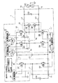
- FIG. 1 is a configuration diagram of a power conversion device according to the present embodiment.
- the power conversion device 1 includes a DC conversion circuit 11, a PWM bridge circuit 12, a power line short circuit 13, a reactor (L2, L3), a capacitor (C1, C2), a DC side terminal T1, and an AC It has a side terminal T2.
- the power conversion device 1 further includes an operation mode switching signal generation unit 20 and first to fourth drive circuits (21 to 24).
- the electric potential of each grounding point (GND) provided in the power converter device 1 does not need to be the same electric potential, and may be different electric potentials. That is, the potentials at the locations of the GND symbols in FIG. 1 (the same applies to FIGS. 3 and 4 described later) may be the same or different.
- the power converter 1 is used in a form in which a DC power source DC is connected to the DC side terminal T1 and an AC power source AC is connected to the AC side terminal T2.
- the DC power source DC may be a secondary battery that charges and discharges DC power, or may be another type of DC power source.
- the AC power supply AC may be a power distribution system, or may be another type of AC power supply. Further, a load may be connected to each terminal together with the DC power source DC or the AC power source AC or instead of the DC power source DC or the AC power source AC.
- the DC conversion circuit 11 is a circuit that performs DC voltage conversion in both directions.
- a bidirectional chopper circuit is employed as a kind of DC conversion circuit.
- the DC conversion circuit 11 includes switching elements (Q1, Q2) and a reactor L1.
- the switching element is an N-channel MOSFET, but other types of switching elements may be employed.
- the source of the switching element Q1 is connected to the drain of the switching element Q2 and one end of the reactor L1.
- the drain of the switching element Q1 is connected to the drains of the switching elements Q3 and Q5 of the PWM bridge circuit 12 and one end of the capacitor C1.
- the source of the switching element Q2 is connected to the sources of the switching elements Q4 and Q6 of the PWM bridge circuit 12, the other end of the capacitor C1, and the negative side of the DC side terminal T1.
- the other end of the reactor L1 is connected to the positive electrode side of the DC side terminal T1.
- Each switching element (Q1, Q2) is connected with a diode such that the anode is connected to the source and the cathode is connected to the drain.
- the DC conversion circuit 11 can convert a DC voltage in both directions by opening / closing operations of each switching element (Q1, Q2) (switching operation between conduction and non-conduction between source and drain). Note that the DC voltage conversion performed by the DC converter circuit 11 may be either step-up or step-down.
- the PWM bridge circuit 12 is a circuit that performs bidirectional power conversion, specifically, DC-AC conversion in one direction and AC-DC conversion in the opposite direction.
- Each switching element Q3 To Q6.
- each switching element Q3 to Q6
- the drain of the switching element Q4 is connected to the source of the switching element Q3, the drain of the switching element Q6 is connected to the source of the switching element Q5, and the drain of the switching element Q3 is connected.
- the drain of the switching element Q5 is connected, and the source of the switching element Q6 is connected to the source of the switching element Q4.
- Each switching element (Q3 to Q6) is connected with a diode in an antiparallel manner, that is, with the anode connected to the source and the cathode connected to the drain.
- the connection point between the switching element Q3 and the switching element Q4 is connected to one of the AC terminals T2 via the reactor L2, and the connection point between the switching element Q5 and the switching element Q6 is connected via the reactor L3. And connected to the other of the AC side terminal T2.
- the PWM bridge circuit 12 can perform bidirectional power conversion by opening and closing the switching elements (Q3 to Q6).
- the PWM bridge circuit 12 has a DC power supply line for transmitting DC power provided on the side close to the DC side terminal T1, and an AC power supply line for transmitting AC power provided on the side close to the AC side terminal T2 (FIG. 1). As shown in FIG. 2, there is an upper side and a lower side).
- the PWM bridge circuit 12 is connected to the reactors L2 and L3 via an AC power supply line.
- the power supply line short circuit 13 is a circuit for realizing a short circuit operation to be described later, and includes switching elements Q7 and Q8.
- the source of the switching element Q7 is connected between the PWM bridge circuit 12 and the reactor L2 (upper AC power supply line), and the drain of the switching element Q7 is connected to the drain of the switching element Q8.
- the source of the switching element Q8 is connected between the PWM bridge circuit 12 and the reactor L3 (lower AC power supply line).
- the switching element Q7 is connected to a diode such that the anode is connected to the source and the cathode is connected to the drain.
- the switching element Q8 is connected to a diode such that the anode is connected to the source and the cathode is connected to the drain.
- the switching element Q7 is closed (conductive state), so that the AC power supply line is short-circuited from the lower side to the upper side. Further, since only the switching element Q8 is closed, the AC power supply line is short-circuited from the upper side to the lower side. Further, when both switching elements Q7 and Q8 are in an open state (non-conductive state), the AC power supply lines are not short-circuited.
- the capacitor C2 has one end connected between the reactor L2 and one AC side terminal T2, and the other end connected between the reactor L3 and the other AC side terminal T2.
- the operation mode switching signal generation unit 20 generates an operation mode switching signal for switching the operation mode (operation mode) of the power conversion device 1.
- the power conversion device 1 has operation modes of “DC-AC conversion mode” and “AC-DC conversion mode”, and any one of them is set alternatively.
- the DC power input from the DC side terminal T1 is subjected to DC-AC conversion from the DC power supply line side to the AC power supply line side using the PWM bridge circuit 12, and the AC side terminal T2 is converted. This is an operation mode that operates so as to output from.
- the AC-DC conversion mode the AC power input from the AC side terminal T2 is subjected to AC-DC conversion from the AC power line side to the DC power line side using the PWM bridge circuit 12, and the DC side terminal This is an operation mode that operates to output from T1.
- the operation mode switching signal generation unit 20 generates an operation mode switching signal for switching the operation mode of the power converter 1 between the DC-AC conversion mode and the AC-DC conversion mode according to a predetermined operation mode switching condition. Generate.
- the operation mode switching condition will be described in detail again.
- the first driving circuit 21 the driving signal S 3 for driving the switching element Q3, and generates a drive signal S 7 for driving the switching element Q7.
- the switching elements Q3 and Q7 respectively, in response to the drive signals S 3 and S 7, and performs opening and closing operations.
- the second drive circuit 22 generates a drive signal S 2 for driving the switching element Q2, a drive signal S 4 for driving the switching element Q4, and a drive signal S 6 for driving the switching element Q6.
- the switching elements Q2, Q4, and Q6, respectively, the driving signals S 2, S 4, and in response to S 6, and performs opening and closing operations.
- Third driving circuit 23 the driving signal S 5 for driving the switching element Q5, and generates a drive signal S 8 for driving the switching element Q8.
- Fourth drive circuit 24 generates the driving signals S 1 for driving the switching element Q1.
- the switching element Q1 is adapted to perform a switching operation in response to the driving signal S 1.
- Each of the drive signals (S 1 to S 8 ) is a pulse signal that can open and close the switching element.
- Each drive circuit of the first drive circuit 21 to the fourth drive circuit 24 (hereinafter referred to as “each drive circuit (21 to 24)”) has a drive control circuit and is given from a drive control circuit (not shown).
- Drive signals S 1 to S 6 are generated in accordance with the instructions.
- This drive control circuit receives the operation mode switching signal from the operation mode switching signal generator 20 and recognizes the current operation mode.
- the drive control circuit issues an instruction to each drive circuit (21-24) so that the operation in the DC-AC conversion mode described above is realized, and each drive circuit (21-24) is instructed. Drive signals S 1 to S 6 are generated.
- the drive control circuit issues an instruction to each drive circuit (21 to 24) so that the operation in the above-described AC-DC conversion mode is realized, and the drive signal S is sent to each drive circuit. 1 to S 6 are generated.
- the power conversion device 1 performs voltage conversion (step-up or step-down) using the DC conversion circuit 11 for the DC power input from the DC side terminal T1, and a PWM bridge.
- DC-AC conversion using the circuit 12 is performed in order, and the operation is performed so as to output from the AC side terminal T2. That is, it operates so as to convert electric power in the right direction in FIG.
- the voltage conversion using the DC conversion circuit 11 is appropriately performed so that a desired AC waveform can be output.
- the AC-DC conversion using the PWM bridge circuit 12 and the DC conversion circuit 11 are performed on the AC power input from the AC-side terminal T2.
- the voltage conversion (step-up or high-voltage) using is sequentially performed and output from the DC side terminal T1. That is, it operates to convert electric power in the left direction in FIG.
- the voltage conversion using the DC conversion circuit 11 is appropriately performed so that a desired voltage value is obtained.
- a drive signal that is a pulse signal may be generated by pulse width modulation (PWM) based on voltage comparison between a predetermined sine wave signal and a triangular wave signal.
- PWM pulse width modulation
- a drive signal may be generated by the same method as in Patent Document 1.
- the power supply line short circuit 13 is provided between the AC power supply lines as described above, and the AC power supply lines can be short-circuited by the opening / closing operation of the switching elements (Q7, Q8).
- drive signals S 7 and the drive signal S 8 is (execution of a short circuit) ON and OFF can also be seen as short-circuit control signal representative of one of (non-execution of the short-circuit).
- Each of the switching elements (Q7, Q8) is closed at the timing when the corresponding short-circuit control signal is turned ON, and the AC power supply lines are short-circuited.
- the short-circuit operation is an operation for short-circuiting between the AC power supply lines under a predetermined condition to make various improvements in the DC-AC conversion of the power.
- the short-circuit operation is an operation in which the AC power supply lines are short-circuited in one direction in synchronization with the polarity of the AC voltage waveform when the PWM bridge circuit 12 performs DC-AC conversion. Specifically, when the AC voltage is a positive value, it is short-circuited upward in FIG. 1, and when the AC voltage is a negative value, it is short-circuited downward in FIG.
- the voltage at both ends of the power supply line short circuit 13 is made three levels, and highly efficient DC-AC conversion becomes possible.
- the content of the short-circuit operation is not limited to this, and for example, it is possible to conform to the operation disclosed in Patent Document 1.
- the power conversion device 1 includes the first drive circuit 21 and the third drive circuit 23 as means (a prohibition means) for preventing the short-circuit operation from being executed when in the AC-DC conversion mode.
- the first drive circuit 21 and the third drive circuit 23 receive the operation mode switching signal from the operation mode switching signal generator 20, and in the AC-DC conversion mode, whichever of the switching elements Q7 and Q8 is selected. Is also fixed to the open state. As a result, the short circuit operation is performed in the DC-AC conversion mode, while the short circuit operation is not performed in the AC-DC conversion mode.
- the operation mode switching signal generation unit 20 generates an operation mode switching signal in accordance with a predetermined operation mode switching condition.
- the operation mode switching condition can be set to various conditions according to the application or use environment of the power conversion device 1. Here, some specific examples of the operation mode switching condition will be described and described below.
- the condition is based on the voltage value Assume that the DC power source DC is a rechargeable secondary battery, for example. In this case, in a situation where the voltage value of the secondary battery is relatively high, the charge amount of the secondary battery is relatively large (thus, the necessity of charging is low at this time), and conversely the voltage value of the secondary battery is compared. In a low situation, it can be said that the amount of charge of the secondary battery is relatively small (therefore, it is highly necessary to charge at the present time).
- the voltage value of the DC power input to the power conversion device 1 (for example, the voltage value between the DC side terminals T1 and reflecting the voltage value of the secondary battery) is detected.
- the voltage value is equal to or higher than the predetermined first threshold value
- an operation mode switching signal for switching to the DC-AC conversion mode is generated, and the voltage value is the same as the predetermined second threshold value (the first threshold value). It is preferable that an operation mode switching signal for switching to the AC-DC conversion mode is generated when the voltage value is equal to or higher than the predetermined first threshold value, an operation mode switching signal for switching to the DC-AC conversion mode is generated, and the voltage value is the same as the predetermined second threshold value (the first threshold value). It is preferable that an operation mode switching signal for switching to the AC-DC conversion mode is generated when
- the DC power source DC is, for example, a solar cell (power source that can sell power to an electric power company, etc.), the AC power source AC is a distribution system, and a DC load ( It is assumed that a heater or the like is connected to the DC side terminal T1.
- the power sale price and the power purchase price may be different, and it is considered preferable for the user of the power conversion device 1 (such as a power consumer) to sell power when the power sale price is higher. Therefore, the operation mode of the power conversion device is set to the DC-AC conversion mode so that the power sale is promoted in the situation where the power sale price is expected to be higher, and in the situation where the power sale price is not expected, the power purchase is promoted. It is preferable to be in an AC-DC conversion mode.
- the selling price tends to be higher or lower depending on the time of day. Therefore, in determining whether the power selling price is expected to be higher, information on the current time zone may be used. That is, the power conversion device 1 has a clock function, grasps the current time zone using the clock function, and switches the operation mode based on the current time zone (for example, the DC-AC conversion mode in the daytime time zone). And in the night time zone, the AC-DC conversion mode may be used).
- the power conversion device 1 receives this information, and based on the information, the power sale price is expected to be higher. You may make it determine whether there exists.
- the power conversion device 1 is provided with an operation switch for accepting a user operation (operation for switching the operation mode).
- the condition may be based on the operation of the operation switch.
- the operation mode switching signal for switching to the DC-AC conversion mode is generated, and when the operation for switching to the AC-DC conversion mode is performed, the AC It is possible to set an operation mode switching condition so that an operation mode switching signal for switching to the DC conversion mode is generated. As a result, the operation mode can be set to reflect the user's intention.
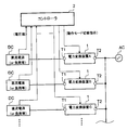
- each controller 2 is used in a state where each power conversion device 1 is connected to the controller 2.
- the controller 2 may give an operation mode switching instruction to each power conversion device 1, and each power conversion device 1 may generate an operation mode switching signal in accordance with this instruction. That is, when the controller 2 gives an instruction to switch to the DC-AC conversion mode, an operation mode switching signal to switch to the DC-AC conversion mode is generated, and an instruction to switch to the AC-DC conversion mode is given.
- the operation mode switching condition can be set so that an operation mode switching signal for switching to the AC-DC conversion mode is generated.
- the controller 2 has a clock function. For example, based on information on the current time zone, the controller 2 performs a DC-AC conversion mode operation (such as an operation of discharging a secondary battery) during the daytime, and AC- at the nighttime. An operation mode switching instruction may be issued to each power conversion device 1 so as to perform an operation in a DC conversion mode (such as an operation of charging a secondary battery).
- a DC-AC conversion mode operation such as an operation of discharging a secondary battery
- An operation mode switching instruction may be issued to each power conversion device 1 so as to perform an operation in a DC conversion mode (such as an operation of charging a secondary battery).
- the controller 2 detects a voltage value of a DC power source (or load) such as a secondary battery connected to each power converter 1, and the voltage value is equal to or higher than a predetermined first threshold value.
- a DC power source or load
- the power conversion device 1 is operated in the DC-AC conversion mode (the operation of discharging the secondary battery), and the voltage value is the same as the predetermined second threshold value (the first threshold value). It is also possible to issue an operation mode switching instruction so that the power conversion device 1 operates in the AC-DC conversion mode (the operation of charging the secondary battery) when Also good.
- controller 2 shown in FIG. 2 is provided outside the power conversion device 1, and gives an operation mode switching instruction from the outside to each power conversion device 1.
- the controller 2 may be provided inside the power conversion device 1.
- the power conversion device 1 itself may have a functional unit (control unit) corresponding to the controller 2.
- the present embodiment is basically the same as the first embodiment except for the point relating to the means for inhibiting the short-circuit operation.
- emphasis is placed on the description of parts different from the first embodiment, and descriptions of parts common to the first embodiment may be omitted.
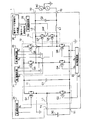
- FIG. 3 is a configuration diagram of the power conversion device according to the present embodiment.
- the power conversion device 1 has two AND circuits (31, 32).
- the operation mode switching signal generation unit 20 represents one of ON (a state representing a logic “1” in the AND circuit) and OFF (a state representing a logic “0” in the AND circuit) as the operation mode switching signal. A signal is generated.
- the ON state represents the DC-AC conversion mode
- the OFF state represents the AC-DC conversion mode.
- the operation mode switching signal transitions from ON to OFF
- the operation mode is switched from DC-AC conversion mode to AC-DC conversion mode.
- the operation mode transition signal transitions from OFF to ON
- the operation mode is AC-DC conversion.
- the mode is switched to the DC-AC conversion mode.
- the AND circuit 31 receives an operation mode switching signal and a drive signal S 7 (short circuit control signal).
- the drive signal S 7 is either ON (state that represents a logic “1” in the AND circuit) that closes the switching element Q7 or OFF (state that represents a logic “0” in the AND circuit) that opens the switching element Q7. Is a pulse signal representing
- the AND circuit 31 outputs a drive signal S 7 ′, which is a logical product of these input signals, to the switching element Q7. That AND circuit 31, the drive signal S 7 instead of the drive signal S 7 'is set to be the drive signal of the switching element Q7.
- the AND circuit 32 receives an operation mode switching signal and a drive signal S 8 (short circuit control signal).
- the drive signal S 8 is either the ON of the switching element Q8 closed OFF to (state representing a logic "1" in the AND circuit) and an open state (state representing a logic "0" in the AND circuit) Is a pulse signal representing
- the AND circuit 32 outputs a drive signal S 8 ′, which is the logical product of these input signals, to the switching element Q8. That AND circuit 32, the drive signal S 8 in place of the drive signal S 8 'is set to be the drive signal of the switching element Q8.
- each AND circuit (31, 32) calculates the logical product of the operation mode switching signal and the short-circuit control signal, so that the short-circuit control signal is fixed to OFF in the AC-DC conversion mode. Has been fixed.
- the switching elements Q7 and Q8 are both fixed in the open state, and the AC power supply line short circuit between the power supply line short circuit 13 is not performed.
- the power conversion apparatus 1 performs a short-circuit operation in the DC-AC conversion mode, and prohibits execution of the short-circuit operation in the AC-DC conversion mode.
- the execution of the short-circuit operation is prohibited by using each AND circuit (31, 32). Therefore, it is not necessary to provide the first drive circuit 21 or the third drive circuit 23 with a function of changing the state of the drive signals (S 7 , S 8 ) according to the operation mode switching signal, and this function is provided in this embodiment. It is not done. Therefore, the configurations and operations of the first drive circuit 21 and the third drive circuit 23 are simpler than those in the first embodiment.
- the form of the AND circuit (31, 32) is not particularly limited.
- the AND circuit may be provided either inside or outside the drive circuit (21, 23).
- an AND circuit as hardware may be provided, and processing of the AND circuit may be performed using software.
- the present embodiment is basically the same as the first embodiment except for the point relating to the means for inhibiting the short-circuit operation.
- emphasis is placed on the description of parts different from the first embodiment, and descriptions of parts common to the first embodiment may be omitted.
- FIG. 4 is a configuration diagram of the power conversion device according to the present embodiment.
- the power conversion device 1 includes a connection switch SW and a fifth drive circuit 25.
- the connection switch SW is provided in a part of the power supply line short circuit 13, and the connection switch SW is opened / closed to switch connection / separation at that point.
- connection switch SW When the connection switch SW is open, the AC power supply line is not short-circuited by the power supply line short circuit 13 regardless of the state of the switching elements Q7 and Q8.
- connection switch SW When the connection switch SW is closed, the AC power supply lines are short-circuited by the power supply line short circuit 13 according to the states of the switching elements Q7 and Q8.
- the fifth drive circuit 25 receives the operation mode switching signal and controls the opening / closing of the connection switch SW in accordance with this signal. That is, when the fifth drive circuit 25 receives the operation mode switching signal for switching to the DC-AC conversion mode, the fifth drive circuit 25 receives the operation mode switching signal for switching to the AC-DC conversion mode by fixing the connection switch SW to the closed state. If the switch is connected, the connection switch SW is switched to the open state and fixed.
- the connection switch SW is fixed in the open state, and a short circuit between the AC power supply lines by the power supply line short circuit 13 is prohibited. Therefore, the power converter 1 is configured to execute a short circuit operation in the DC-AC conversion mode, and is prohibited from performing the short circuit operation in the AC-DC conversion mode.
- a semiconductor switching element or the like can be used as the connection switch SW. Also, unlike other switching elements, it does not require very high speed opening and closing, so it is possible to use a mechanical switch such as a relay. When a semiconductor switching element is used, it is necessary to use a device that conducts bidirectionally in the closed state and completely shuts off in the open state, such as a reverse blocking IGBT.
- connection switch SW is provided between the switching elements (Q7, Q8), between the upper AC power supply line and the switching element Q7, or at the lower AC. It may be between the power supply line and the switching element Q8.
- the prohibition of the short-circuit operation is realized by using the connection switch SW. Therefore, it is not necessary to provide the first drive circuit 21 or the third drive circuit 23 with a function of changing the state of the drive signals (S 7 , S 8 ) according to the operation mode switching signal, and this function is provided in this embodiment. It is not done. Therefore, the configurations and operations of the first drive circuit 21 and the third drive circuit 23 are simpler than those in the first embodiment.
- the power conversion device 1 includes the PWM bridge circuit 12 between the DC power supply line and the AC power supply line, and the AC power supply line from the DC power supply line side using the PWM bridge circuit 12.
- DC-AC conversion mode for performing DC-AC conversion to the side, and AC-DC conversion mode for performing AC-DC conversion from the AC power supply line side to the DC power supply line side using the PWM bridge circuit 12 have.
- the power conversion device 1 is provided between the AC power supply lines, and performs a short circuit operation for short-circuiting the AC power supply lines.
- the power line short circuit 13 a function unit (operation mode switching unit) for switching the operation mode, and an AC ⁇ And a functional unit (short-circuit operation prohibiting unit) that prevents the short-circuit operation from being executed in the DC conversion mode.
- the short-circuit operation is not performed in the AC-DC conversion mode. Therefore, while it is possible to enjoy the advantages of the short-circuit operation, it is possible to prevent problems caused by the short-circuit operation being performed during the AC-DC conversion operation.
- the present invention can be used for a power conversion device that converts power bidirectionally.
Abstract
短絡動作による利点を享受することが可能でありながら、交流-直流変換の動作時に短絡動作が行われることによる不具合を、防止することが可能となる電力変換装置を提供する。直流電源ラインと交流電源ラインの間にブリッジ回路を備え、該ブリッジ回路を用いて直流電源ライン側から交流電源ライン側への直流-交流変換を行う直流-交流変換モード、および、該ブリッジ回路を用いて交流電源ライン側から直流電源ライン側への交流-直流変換を行う交流-直流変換モード、の動作モードを有し、交流電源ライン間に設けられ、交流電源ライン間を短絡させる短絡動作を実行する、電源ライン短絡回路と、動作モードを切替える動作モード切替部と、交流-直流変換モードであるときに、短絡動作が実行されないようにする短絡動作禁止部と、を備えた電力変換装置とする。
Description
本発明は、双方向に電力変換を行う電力変換装置に関する。
従来、電力変換に用いられる各種のインバータ装置などが提案されている。その一つとして特許文献1には、フルブリッジインバータを備えたインバータ装置であって、電源ライン短絡回路を有するものが提案されている。このインバータ装置は、所定の条件下、即ち、フルブリッジインバータに対する駆動パルス信号がオフ期間で、フルブリッジインバータの出力電流が下降するときに、電源ライン短絡回路によって電源ライン間を短絡させる。
このような動作が行われることにより、フルブリッジインバータの出力電流に生じるリップルをその出力電流の平均値が零となる辺りで小さくすることができ、直流から交流への変換効率の向上およびノイズの低減が図られる。また更に、直流電源回路への電流の逆流を防ぎ、直流電源回路の負側出力端の電位の変動幅を小さく抑えて、漏洩電流を低減させることが可能である。
上記した特許文献1は、電力の直流-交流変換を伴う系統連系動作時に、所定の条件下で電源ライン間を短絡させる動作(短絡動作)を行い、各種改善が図られるようにしたものである。
ここで、一方向への直流-交流変換(系統連系動作など)だけでなく、その逆方向への交流-直流変換(整流動作など)をも行うようにした双方向電力変換装置について考える。双方向電力変換装置においても、上記したような電源ライン短絡回路を設けておき、直流-交流変換の動作時に短絡動作が行われるようにすることで、上述したような改善効果を得ることが可能である。
しかしながら、交流-直流変換の動作時に短絡動作が実行されると、電力変換の動作に不具合を来たすことになる。
本発明は、この問題に鑑み、短絡動作による利点を享受することが可能でありながら、交流-直流変換の動作時に短絡動作が行われることによる不具合を、防止することが可能となる電力変換装置の提供を目的とする。
上記目的を達成するため、本発明に係る電力変換装置は、直流電源ラインと交流電源ラインの間に設けられたブリッジ回路を備え、前記ブリッジ回路を用いて直流電源ライン側から交流電源ライン側への直流-交流変換を行う直流-交流変換モード、および、前記ブリッジ回路を用いて前記交流電源ライン側から前記直流電源ライン側への交流-直流変換を行う交流-直流変換モード、の動作モードを有する電力変換装置であって、前記交流電源ライン間に設けられ、前記交流電源ライン間を短絡させる短絡動作を実行する電源ライン短絡回路と、前記動作モードを切替える動作モード切替部と、前記交流-直流変換モードであるときに、前記短絡動作が実行されないようにする短絡動作禁止部と、を備えた構成とする。
本構成によれば、短絡動作が行われる一方で、交流-直流変換モードであるときには短絡動作の実行は行われない。そのため、短絡動作による利点を享受することが可能でありながら、交流-直流変換の動作時に短絡動作が行われることによる不具合を防止することが可能となる。
また上記構成としてより具体的には、前記ブリッジ回路は、スイッチング素子がブリッジ接続されて形成されており、前記交流電源ラインを介してリアクタに接続されているものであって、前記電源ライン短絡回路は、前記短絡動作により、前記ブリッジ回路と前記リアクタとの間において、前記交流電源ライン間を短絡させる構成としてもよい。
また上記構成としてより具体的には、入力される直流電力の電圧値を検出する電圧検出部と、を更に備え、前記動作モード切替部は、前記検出の結果に基づいて、前記動作モードを切替える構成としても良い。
また上記構成としてより具体的には、ユーザによって操作される操作スイッチと、を更に備え、前記動作モード切替部は、前記操作スイッチの操作に基づいて、前記動作モードを切替える構成としても良い。
また上記構成としてより具体的には、前記動作モード切替部は、現在の時間帯に基づいて、前記動作モードを切替える構成としても良い。
また上記構成としてより具体的には、前記動作モード切替部は、外部から与えられる動作モード切替指示に応じて、前記動作モードを切替える構成としても良い。
また上記構成としてより具体的には、前記電源ライン短絡回路は、ONとOFFの何れか一方を表す短絡制御信号を受取るようになっており、前記短絡制御信号のONのタイミングで前記交流電源ライン間を短絡させることにより、前記短絡動作を行う構成としても良い。
また上記構成において、前記動作モード切替部は、前記動作モードに応じてONとOFFが切替えられる動作モード切替信号を出力するようになっており、前記短絡動作禁止部は、前記動作モード切替信号と前記短絡制御信号との論理積を算出することにより、交流-直流変換モードであるときにはOFFに固定されるように、前記短絡制御信号を修正する構成としてもよい。
また上記構成において、前記電源ライン短絡回路の一部に介在して設けられ、前記一部の箇所の接続と分離を切替えるように開閉する接続スイッチと、を更に備え、前記短絡動作禁止部は、前記交流-直流変換モードであるときには、前記接続スイッチを開状態に固定する構成としてもよい。
本発明に係る電力変換装置によれば、短絡動作が行われる一方で、交流-直流変換モードであるときには短絡動作の実行は行われない。そのため、短絡動作による利点を享受することが可能でありながら、交流-直流変換の動作時に短絡動作が行われることによる不具合を防止することが可能となる。
本発明の実施形態について、第1実施形態から第3実施形態の各々を例に挙げて、以下に説明する。
1.第1実施形態
[電力変換装置の構成等について]
まず第1実施形態について説明する。図1は、本実施形態に係る電力変換装置の構成図である。本図に示すように当該電力変換装置1は、直流変換回路11、PWMブリッジ回路12、電源ライン短絡回路13、リアクタ(L2,L3)、コンデンサ(C1、C2)、直流側端子T1、および交流側端子T2を有している。また電力変換装置1は、動作モード切替信号生成部20、および第1~第4駆動回路(21~24)を更に有している。なお、電力変換装置1に設けられている各接地点(GND)の電位は、互いに同じ電位である必要は無く、異なる電位であっても良い。すなわち図1(後述する図3および図4についても同様)における各GND記号の箇所の電位は、互いに同じであっても良く、異なっていても良い。
なお電力変換装置1は、直流側端子T1には直流電源DCが接続され、交流側端子T2には交流電源ACが接続された形態で使用される。直流電源DCは、直流電力の充放電を行う二次電池であっても良く、その他の種類の直流電源であっても良い。また交流電源ACは、配電系統であっても良く、その他の種類の交流電源であっても良い。また各端子には、直流電源DC又は交流電源ACとともに、或いは直流電源DC又は交流電源ACに代えて負荷が接続されても構わない。
直流変換回路11は、双方向に直流電圧の変換を行う回路である。本実施形態では、直流変換回路の一種として、双方向チョッパ回路が採用されている。直流変換回路11は、スイッチング素子(Q1、Q2)、およびリアクタL1を有している。なお本発明の各実施形態では、スイッチング素子はNチャネル型MOSFETであるとするが、他種のものが採用されていても構わない。
スイッチング素子Q1のソースはスイッチング素子Q2のドレインとリアクタL1の一端に接続されている。スイッチング素子Q1のドレインは、PWMブリッジ回路12のスイッチング素子Q3とQ5のドレイン、およびコンデンサC1の一端に接続されている。スイッチング素子Q2のソースは、PWMブリッジ回路12のスイッチング素子Q4とQ6のソース、コンデンサC1の他端、および直流側端子T1の負極側に接続されている。また、リアクタL1の他端は、直流側端子T1の正極側に接続されている。
なお各スイッチング素子(Q1、Q2)には、アノードがソースに接続され、カソードがドレインに接続されるようにして、ダイオードが接続されている。直流変換回路11は、各スイッチング素子(Q1、Q2)の開閉動作(ソース-ドレイン間における導通/非導通の切替動作)によって、双方向に直流電圧を変換することが可能である。なお直流変換回路11が行う直流電圧の変換は、昇圧と降圧の何れであっても構わない。
PWMブリッジ回路12は、双方向の電力変換、具体的には一方向へは直流-交流変換、その逆方向へは交流-直流変換を行う回路であり、フルブリッジ接続された各スイッチング素子(Q3~Q6)を有している。
各スイッチング素子(Q3~Q6)の接続形態としては、スイッチング素子Q3のソースにスイッチング素子Q4のドレインが接続され、スイッチング素子Q5のソースにスイッチング素子Q6のドレインが接続され、スイッチング素子Q3のドレインにスイッチング素子Q5のドレインが接続され、スイッチング素子Q4のソースにスイッチング素子Q6のソースが接続されている。なお各スイッチング素子(Q3~Q6)には、逆並列の形態で、即ちアノードがソースに接続され、カソードがドレインに接続されるようにして、ダイオードが接続されている。
また、スイッチング素子Q3とスイッチング素子Q4との接続点は、リアクタL2を介して、交流側端子T2の一方に接続されており、スイッチング素子Q5とスイッチング素子Q6との接続点は、リアクタL3を介して、交流側端子T2の他方に接続されている。PWMブリッジ回路12は、各スイッチング素子(Q3~Q6)の開閉動作によって、双方向の電力変換を行うことが可能である。
なおPWMブリッジ回路12は、直流側端子T1に近い側に設けられた直流電力を伝送する直流電源ラインと、交流側端子T2に近い側に設けられた交流電力を伝送する交流電源ライン(図1に示すように、上側と下側がある)との間に、設けられている。またPWMブリッジ回路12は、交流電源ラインを介してリアクタL2およびL3に接続されている。
電源ライン短絡回路13は、後述する短絡動作を実現させるための回路であり、スイッチング素子Q7およびQ8を有している。スイッチング素子Q7のソースは、PWMブリッジ回路12とリアクタL2の間(上側の交流電源ライン)に接続されており、スイッチング素子Q7のドレインは、スイッチング素子Q8のドレインに接続されている。またスイッチング素子Q8のソースは、PWMブリッジ回路12とリアクタL3の間(下側の交流電源ライン)に接続されている。
なおスイッチング素子Q7には、アノードがソースに接続され、カソードがドレインに接続されるようにして、ダイオードが接続されている。またスイッチング素子Q8には、アノードがソースに接続され、カソードがドレインに接続されるようにして、ダイオードが接続されている。
電源ライン短絡回路13によれば、スイッチング素子Q7のみが閉状態(導通状態)となることで、交流電源ラインは下側から上側の方向について短絡する。またスイッチング素子Q8のみが閉状態となることで、交流電源ラインは上側から下側の方向について短絡する。またスイッチング素子Q7とQ8の何れもが開状態(非導通状態)であるときは、交流電源ライン間は短絡しない。
またコンデンサC2は、一端がリアクタL2と一方の交流側端子T2との間に接続され、他端がリアクタL3と他方の交流側端子T2との間に接続されている。
動作モード切替信号生成部20は、電力変換装置1の動作モード(動作形態)を切替えるための動作モード切替信号を生成する。なお電力変換装置1は、「直流-交流変換モード」と「交流-直流変換モード」の各動作モードを有しており、何れかが択一的に設定される。
直流-交流変換モードは、直流側端子T1から入力される直流電力に対して、PWMブリッジ回路12を用いて直流電源ライン側から交流電源ライン側への直流-交流変換を行い、交流側端子T2から出力するように動作する動作モードである。また交流-直流変換モードは、交流側端子T2から入力される交流電力に対して、PWMブリッジ回路12を用いて交流電源ライン側から直流電源ライン側への交流-直流変換を行い、直流側端子T1から出力するように動作する動作モードである。
動作モード切替信号生成部20は、予め決められた動作モード切替条件に従い、電力変換装置1の動作モードを直流-交流変換モードと交流-直流変換モードとの間で切替えるための動作モード切替信号を生成する。なお動作モード切替条件については、改めて詳細に説明する。
第1駆動回路21は、スイッチング素子Q3を駆動させるための駆動信号S3、および、スイッチング素子Q7を駆動させるための駆動信号S7を生成する。なお、スイッチング素子Q3およびQ7は、それぞれ、駆動信号S3およびS7に応じて、開閉動作を行うようになっている。
第2駆動回路22は、スイッチング素子Q2を駆動させるための駆動信号S2、スイッチング素子Q4を駆動させるための駆動信号S4、および、スイッチング素子Q6を駆動させるための駆動信号S6を生成する。なお、スイッチング素子Q2、Q4、およびQ6は、それぞれ、駆動信号S2、S4、およびS6に応じて、開閉動作を行うようになっている。
第3駆動回路23は、スイッチング素子Q5を駆動させるための駆動信号S5、および、スイッチング素子Q8を駆動させるための駆動信号S8を生成する。なお、スイッチング素子Q5およびQ8は、それぞれ、駆動信号S5およびS8に応じて、開閉動作を行うようになっている。
第4駆動回路24は、スイッチング素子Q1を駆動させるための駆動信号S1を生成する。なお、スイッチング素子Q1は、駆動信号S1に応じて開閉動作を行うようになっている。また各駆動信号(S1~S8)は、何れもスイッチング素子を開閉動作させることが可能なパルス信号である。
[基本動作について]
第1駆動回路21~第4駆動回路24の各駆動回路(以下、「各駆動回路(21~24)」という)は、それぞれ駆動制御回路を有し、駆動制御回路(不図示)から与えられる指示に従って、駆動信号S1~S6を生成するようになっている。この駆動制御回路は、動作モード切替信号生成部20から動作モード切替信号を受取って、現在の動作モードを認識する。
第1駆動回路21~第4駆動回路24の各駆動回路(以下、「各駆動回路(21~24)」という)は、それぞれ駆動制御回路を有し、駆動制御回路(不図示)から与えられる指示に従って、駆動信号S1~S6を生成するようになっている。この駆動制御回路は、動作モード切替信号生成部20から動作モード切替信号を受取って、現在の動作モードを認識する。
駆動制御回路は、直流-交流変換モードにおいては、上記した直流-交流変換モードの動作が実現されるように各駆動回路(21~24)に指示を出し、各駆動回路(21~24)に駆動信号S1~S6を生成させる。一方、駆動制御回路は、交流-直流変換モードにおいては、先述した交流-直流変換モードの動作が実現されるように各駆動回路(21~24)に指示を出し、各駆動回路に駆動信号S1~S6を生成させる。
これにより電力変換装置1は、直流-交流変換モードのときは、直流側端子T1から入力される直流電力に対して、直流変換回路11を用いた電圧変換(昇圧または降圧)、および、PWMブリッジ回路12を用いた直流-交流変換を順に行い、交流側端子T2から出力するように動作する。すなわち、図1における右方向に向かって電力を変換するように動作する。なお直流変換回路11を用いた電圧変換は、所望の交流波形が出力可能となるように適切に行われる。
その一方で電力変換装置1は、交流-直流変換モードのときは、交流側端子T2から入力される交流電力に対して、PWMブリッジ回路12を用いた交流-直流変換、および、直流変換回路11を用いた電圧変換(昇圧または高圧)を順に行い、直流側端子T1から出力するように動作する。すなわち、図1における左方向に向かって電力を変換するように動作する。なお直流変換回路11を用いた電圧変換は、所望の電圧値が得られるように適切に行われる。
なお、各駆動回路(21~24)が駆動信号S1~S6を生成する手法については、既に知られている種々の手法に準じたものとすることが出来る。例えば、所定の正弦波信号と三角波信号との電圧比較に基づくパルス幅変調(PWM)により、パルス信号である駆動信号が生成されるようにしても良い。また直流-交流変換モードの際には、特許文献1の場合と同様の手法により、駆動信号が生成されるようにしても良い。
[短絡動作について]
電源ライン短絡回路13は、上記したように交流電源ライン間に設けられており、スイッチング素子(Q7、Q8)の開閉動作によって、この交流電源ライン間を短絡させることが可能である。第1駆動回路21および第3駆動回路23は、所定の短絡動作が実行されるように、それぞれ、駆動信号S7および駆動信号S8を生成するようになっている。
電源ライン短絡回路13は、上記したように交流電源ライン間に設けられており、スイッチング素子(Q7、Q8)の開閉動作によって、この交流電源ライン間を短絡させることが可能である。第1駆動回路21および第3駆動回路23は、所定の短絡動作が実行されるように、それぞれ、駆動信号S7および駆動信号S8を生成するようになっている。
なお駆動信号S7および駆動信号S8は、ON(短絡の実行)とOFF(短絡の不実行)の何れか一方を表す短絡制御信号と見ることも出来る。各スイッチング素子(Q7、Q8)は、対応する短絡制御信号のONのタイミングで閉状態となり、交流電源ライン間を短絡させることになる。
ここで、短絡動作は、所定の条件下で交流電源ライン間を短絡させ、電力の直流-交流変換についての各種改善を図るための動作である。一例として短絡動作は、PWMブリッジ回路12で直流-交流変換を行う際に、交流電圧波形の極性に同期して、交流電源ライン間を片方向に短絡させる動作である。具体的には、交流電圧が正値の時は図1での上向きに短絡させ、交流電圧が負値の時は図1での下向きに短絡させる。
このような内容の短絡動作によれば、電源ライン短絡回路13の両端の電圧を3レベル化し、高効率な直流-交流変換が可能となる。なお短絡動作の内容はこれに限定されるものではなく、例えば特許文献1に開示された動作に準じたものとすること等も可能である。
但し短絡動作は、直流-交流変換モードにおいて実行される場合は、各種改善の効果が得られるが、交流-直流変換モードにおいて実行されると、電力変換の動作に不具合を来たすことになる。そこで電力変換装置1は、交流-直流変換モードであるときに、短絡動作が実行されないようにする手段(禁止する手段)としての第1駆動回路21および第3駆動回路23を備えている。
本実施形態では、第1駆動回路21および第3駆動回路23は、動作モード切替信号生成部20から動作モード切替信号が入力され、交流-直流変換モードにおいては、スイッチング素子Q7とQ8の何れについても開状態に固定するようになっている。これにより、直流-交流変換モードにおいては短絡動作が実行される一方、交流-直流変換モードにおいては短絡動作が実行されないようになっている。
[動作モード切替条件について]
上記した通り、動作モード切替信号生成部20は、予め決められた動作モード切替条件に従い、動作モード切替信号を生成する。動作モード切替条件は、電力変換装置1の用途や使用環境などに応じて、様々な条件としておくことが可能である。ここでは、動作モード切替条件の具体例を幾つか挙げ、以下に説明する。
上記した通り、動作モード切替信号生成部20は、予め決められた動作モード切替条件に従い、動作モード切替信号を生成する。動作モード切替条件は、電力変換装置1の用途や使用環境などに応じて、様々な条件としておくことが可能である。ここでは、動作モード切替条件の具体例を幾つか挙げ、以下に説明する。
(1)電圧値に基づいた条件とする場合
直流電源DCが、例えば充放電の可能な二次電池である場合を想定する。この場合、二次電池の電圧値が比較的高い状況では、二次電池の充電量は比較的多く(よって、現時点では充電を行う必要性は低い)、逆に二次電池の電圧値が比較的低い状況では、二次電池の充電量は比較的少ない(よって、現時点では充電を行う必要性が高い)と言える。
直流電源DCが、例えば充放電の可能な二次電池である場合を想定する。この場合、二次電池の電圧値が比較的高い状況では、二次電池の充電量は比較的多く(よって、現時点では充電を行う必要性は低い)、逆に二次電池の電圧値が比較的低い状況では、二次電池の充電量は比較的少ない(よって、現時点では充電を行う必要性が高い)と言える。
この観点から見れば、電力変換装置1が入力される直流電力の電圧値(例えば各直流側端子T1間の電圧値であり、二次電池の電圧値を反映している)を検出するようにしておき、当該電圧値が所定の第1閾値以上であるときに、直流-交流変換モードに切替える動作モード切替信号が生成され、当該電圧値が所定の第2閾値(第1閾値と同じであってもよい)以下であるときに、交流-直流変換モードに切替える動作モード切替信号が生成されることが好ましい。
そこで、このように動作モード切替信号が生成されるように、動作モード切替条件を設定しておくことが可能である。これにより、二次電池の充電量を適切な状態に維持することが容易となる。
(2)売電価格等に応じた条件とする場合
直流電源DCが例えば太陽電池(電力会社等への売電が可能な電源)であり、交流電源ACが配電系統であって、直流負荷(ヒータ等)が直流側端子T1に接続されている場合を想定する。売電価格と買電価格は異なることがあり、電力変換装置1の利用者(電力の需要家等)にとっては、売電価格の方が高いときに売電を行うことが好ましいと考えられる。そこで電力変換装置の動作モードは、売電価格の方が高くなると見込まれる状況では、売電が促進されるように直流-交流変換モードとなり、そうでない状況では、買電が促進されるように交流-直流変換モードとなることが好ましい。
直流電源DCが例えば太陽電池(電力会社等への売電が可能な電源)であり、交流電源ACが配電系統であって、直流負荷(ヒータ等)が直流側端子T1に接続されている場合を想定する。売電価格と買電価格は異なることがあり、電力変換装置1の利用者(電力の需要家等)にとっては、売電価格の方が高いときに売電を行うことが好ましいと考えられる。そこで電力変換装置の動作モードは、売電価格の方が高くなると見込まれる状況では、売電が促進されるように直流-交流変換モードとなり、そうでない状況では、買電が促進されるように交流-直流変換モードとなることが好ましい。
この観点から見れば、電力変換装置1が売電価格の方が高くなると見込まれる状況であるかを判定するようにしておき、高くなると見込まれるときに、直流-交流変換モードに切替える動作モード切替信号が生成され、そうでないときに、交流-直流変換モードに切替える動作モード切替信号が生成されることが好ましい。そこで、このように動作モード切替信号が生成されるように、動作モード切替条件を設定しておくことが可能である。
なお多くの場合、時間帯によって、売電価格の方が高くなったり低くなったりする傾向がある。そのため、売電価格の方が高くなると見込まれる状況であるかを判定するにあたっては、現在の時間帯の情報を用いるようにしても良い。すなわち電力変換装置1は、時計機能を有し、時計機能を用いて現在の時間帯を把握し、現在の時間帯に基づいて動作モードを切替える(例えば、昼間の時間帯では直流-交流変換モードとし、夜間の時間帯では交流-直流変換モードとする)ようにしても良い。
また、電力会社等が売買電価格の情報を送信するようになっている場合、電力変換装置1はこの情報を受信し、当該情報に基づいて、売電価格の方が高くなると見込まれる状況であるかを判定するようにしても良い。
(3)操作スイッチの操作に基づく条件とする場合
また電力変換装置1に、ユーザの操作(動作モードを切替えるための操作)を受付けるための操作スイッチを設けておき、動作モード切替条件を、この操作スイッチの操作に基づいた条件としても良い。
また電力変換装置1に、ユーザの操作(動作モードを切替えるための操作)を受付けるための操作スイッチを設けておき、動作モード切替条件を、この操作スイッチの操作に基づいた条件としても良い。
すなわち、直流-交流変換モードに切替えるための操作がなされたときは、直流-交流変換モードに切替える動作モード切替信号が生成され、交流-直流変換モードに切替えるための操作がなされたときは、交流-直流変換モードに切替える動作モード切替信号が生成されるように、動作モード切替条件を設定しておくことが可能である。これにより、ユーザの意図を反映させるように、動作モードを設定することが可能となる。
(4)コントローラの指示に基づく条件とする場合
また電力変換装置1の使用形態としては、例えば図2に示すように、一または複数の電力変換装置1(図2では、電力変換装置A~Cを例示している)を制御するコントローラ2が設けられ、それぞれの電力変換装置1が、コントローラ2に接続された状態で使用されることがある。
また電力変換装置1の使用形態としては、例えば図2に示すように、一または複数の電力変換装置1(図2では、電力変換装置A~Cを例示している)を制御するコントローラ2が設けられ、それぞれの電力変換装置1が、コントローラ2に接続された状態で使用されることがある。
この場合、コントローラ2が、各電力変換装置1に対して動作モード切替指示を与えるようにしておき、各電力変換装置1は、この指示に従って、動作モード切替信号を生成するようにしても良い。すなわちコントローラ2から、直流-交流変換モードに切替える旨の指示がなされたときは、直流-交流変換モードに切替える動作モード切替信号が生成され、交流-直流変換モードに切替える旨の指示がなされたときは、交流-直流変換モードに切替える動作モード切替信号が生成されるように、動作モード切替条件を設定しておくことが可能である。
なおコントローラ2は、時計機能を有し、例えば現在の時間帯の情報に基づき、昼間においては直流-交流変換モードの動作(二次電池を放電する動作など)を行わせ、夜間においては交流-直流変換モードの動作(二次電池を充電する動作など)を行わせるように、各電力変換装置1に動作モード切替指示を出すようにしても良い。
またコントローラ2は、図2に示すように各電力変換装置1に接続されている二次電池などの直流電源(或いは負荷)の電圧値を検出し、当該電圧値が所定の第1閾値以上であるときに、その電力変換装置1に対しては直流-交流変換モードの動作(二次電池を放電する動作)を行わせ、当該電圧値が所定の第2閾値(第1閾値と同じであってもよい)以下であるときに、その電力変換装置1に対しては交流-直流変換モードの動作(二次電池を充電する動作)を行わせるように、動作モード切替指示を出すようにしても良い。
なお図2に示すコントローラ2は、電力変換装置1の外部に設けられており、各電力変換装置1に対して、外部から動作モード切替指示を与えるようになっている。但しコントローラ2は、電力変換装置1の内部に設けられていても構わない。また電力変換装置1自体が、コントローラ2に相当する機能部(制御部)を有していても構わない。
2.第2実施形態
次に第2実施形態について説明する。なお本実施形態は、短絡動作を禁止するための手段に関する点を除き、基本的には第1実施形態と同等である。以下の説明においては、第1実施形態と異なる部分の説明に重点を置き、第1実施形態と共通する部分の説明については省略することがある。
次に第2実施形態について説明する。なお本実施形態は、短絡動作を禁止するための手段に関する点を除き、基本的には第1実施形態と同等である。以下の説明においては、第1実施形態と異なる部分の説明に重点を置き、第1実施形態と共通する部分の説明については省略することがある。
図3は、本実施形態に係る電力変換装置の構成図である。本図に示すように、当該電力変換装置1は、二つのAND回路(31、32)を有している。また動作モード切替信号生成部20は、動作モード切替信号として、ON(AND回路において論理「1」を表す状態)とOFFの(AND回路において論理「0」を表す状態)の何れか一方を表す信号を生成するようになっている。
なおONの状態は、直流-交流変換モードを表し、OFFの状態は、交流-直流変換モードを表している。動作モード切替信号がONからOFFに遷移したときは、動作モードは直流-交流変換モードから交流-直流変換モードに切替えられ、逆にOFFからONに遷移したときは、動作モードは交流-直流変換モードから直流-交流変換モードに切替えられることになる。
AND回路31は、動作モード切替信号および駆動信号S7(短絡制御信号)が入力されるようになっている。なお駆動信号S7は、スイッチング素子Q7を閉状態とするON(AND回路において論理「1」を表す状態)と開状態とするOFF(AND回路において論理「0」を表す状態)の何れか一方を表すパルス信号である。
AND回路31は、入力されるこれらの信号の論理積である駆動信号S7´を、スイッチング素子Q7に出力する。つまりAND回路31は、駆動信号S7の代わりに駆動信号S7´が、スイッチング素子Q7の駆動信号となるようにする。
これにより、直流-交流変換モード(動作モード切替信号がONの期間)においては、駆動信号S7と同じ内容の駆動信号S7´が、スイッチング素子Q7に出力される。一方で、交流-直流変換モード(動作モード切替信号がOFFの期間)においては、駆動信号S7の内容に関わらずOFFに固定された駆動信号S7´が、スイッチング素子Q7に出力される。
またAND回路32は、動作モード切替信号および駆動信号S8(短絡制御信号)が入力されるようになっている。なお駆動信号S8は、スイッチング素子Q8を閉状態とするON(AND回路において論理「1」を表す状態)と開状態とするOFF(AND回路において論理「0」を表す状態)の何れか一方を表すパルス信号である。
AND回路32は、入力されるこれらの信号の論理積である駆動信号S8´を、スイッチング素子Q8に出力する。つまりAND回路32は、駆動信号S8の代わりに駆動信号S8´が、スイッチング素子Q8の駆動信号となるようにする。
これにより、直流-交流変換モード(動作モード切替信号がONの期間)においては、駆動信号S8と同じ内容の駆動信号S8´が、スイッチング素子Q8に出力される。一方で、交流-直流変換モード(動作モード切替信号がOFFの期間)においては、駆動信号S8の内容に関わらずOFFに固定された駆動信号S8´が、スイッチング素子Q8に出力される。
このように各AND回路(31、32)は、動作モード切替信号と短絡制御信号との論理積を算出することにより、交流-直流変換モードであるときにはOFFに固定されるように、短絡制御信号を修正するようになっている。
そのため交流-直流変換モードにおいては、スイッチング素子Q7およびQ8は何れも開状態に固定され、電源ライン短絡回路13による交流電源ライン間の短絡は、行われないようになっている。これにより電力変換装置1は、直流-交流変換モードにおいては短絡動作が実行され、交流-直流変換モードにおいては、短絡動作の実行が禁止されるようになっている。
なお本実施形態では、各AND回路(31、32)を利用して、短絡動作の実行の禁止を実現させるようになっている。そのため、第1駆動回路21や第3駆動回路23に、動作モード切替信号に応じて駆動信号(S7、S8)の状態を変える機能を設ける必要は無く、本実施形態では当該機能は設けられていない。そのため、第1駆動回路21や第3駆動回路23の構成や動作は、第1実施形態の場合に比べて簡潔となっている。
またAND回路(31、32)の形態は特に限定されない。例えばAND回路は、駆動回路(21、23)の内部と外部の何れに設けられていても良い。またハードウェアとしてのAND回路が設けられても良く、AND回路の処理がソフトウェアを用いて行われるようにしても良い。
3.第3実施形態
次に第3実施形態について説明する。なお本実施形態は、短絡動作を禁止するための手段に関する点を除き、基本的には第1実施形態と同等である。以下の説明においては、第1実施形態と異なる部分の説明に重点を置き、第1実施形態と共通する部分の説明については省略することがある。
次に第3実施形態について説明する。なお本実施形態は、短絡動作を禁止するための手段に関する点を除き、基本的には第1実施形態と同等である。以下の説明においては、第1実施形態と異なる部分の説明に重点を置き、第1実施形態と共通する部分の説明については省略することがある。
図4は、本実施形態に係る電力変換装置の構成図である。本図に示すように、当該電力変換装置1は、接続スイッチSWおよび第5駆動回路25を有している。接続スイッチSWは、電源ライン短絡回路13の一部に介在して設けられており、接続スイッチSW自身が開閉することにより、その箇所の接続/分離を切替える。
接続スイッチSWが開いているときは、スイッチング素子Q7およびQ8の状態に関わらず、電源ライン短絡回路13によって交流電源ライン間が短絡されることはない。また接続スイッチSWが閉じているときは、スイッチング素子Q7およびQ8の状態に応じ、電源ライン短絡回路13によって交流電源ライン間が短絡されることになる。
また第5駆動回路25は、動作モード切替信号を受取り、この信号に応じて接続スイッチSWの開閉を制御する。すなわち第5駆動回路25は、直流-交流変換モードに切替える動作モード切替信号を受取ったときは、接続スイッチSWを閉状態に切替えて固定し、交流-直流変換モードに切替える動作モード切替信号を受取ったときは、接続スイッチSWを開状態に切替えて固定する。
このように、交流-直流変換モードの期間においては、接続スイッチSWは開状態に固定され、電源ライン短絡回路13による交流電源ライン間の短絡は禁止される。そのため電力変換装置1は、直流-交流変換モードにおいては短絡動作が実行されるようにし、交流-直流変換モードにおいては、短絡動作の実行が禁止されるようになっている。
なお接続スイッチSWとしては、半導体スイッチング素子などを用いることが可能である。また他のスイッチング素子とは異なり、あまり高速な開閉を必要としないため、リレー等の機械的なスイッチを用いることも可能である。なお半導体スイッチング素子を用いる場合は、逆阻止IGBT等のように、閉状態では双方向に導通し、開状態では完全に遮断するものを用いる必要がある。
また接続スイッチSWを設ける位置については、図4に示すように各スイッチング素子(Q7、Q8)同士の間とする他、上側の交流電源ラインとスイッチング素子Q7との間、或いは、下側の交流電源ラインとスイッチング素子Q8との間としても構わない。
なお本実施形態では、接続スイッチSWを利用して、短絡動作の実行の禁止を実現させるようになっている。そのため、第1駆動回路21や第3駆動回路23に、動作モード切替信号に応じて駆動信号(S7、S8)の状態を変える機能を設ける必要は無く、本実施形態では当該機能は設けられていない。そのため、第1駆動回路21や第3駆動回路23の構成や動作は、第1実施形態の場合に比べて簡潔となっている。
4.その他
以上に説明した通り、各実施形態に係る電力変換装置1は、直流電源ラインと交流電源ラインの間にPWMブリッジ回路12を備え、PWMブリッジ回路12を用いて直流電源ライン側から交流電源ライン側への直流-交流変換を行う直流-交流変換モード、および、PWMブリッジ回路12を用いて交流電源ライン側から直流電源ライン側への交流-直流変換を行う交流-直流変換モード、の動作モードを有している。
以上に説明した通り、各実施形態に係る電力変換装置1は、直流電源ラインと交流電源ラインの間にPWMブリッジ回路12を備え、PWMブリッジ回路12を用いて直流電源ライン側から交流電源ライン側への直流-交流変換を行う直流-交流変換モード、および、PWMブリッジ回路12を用いて交流電源ライン側から直流電源ライン側への交流-直流変換を行う交流-直流変換モード、の動作モードを有している。
また電力変換装置1は、交流電源ライン間に設けられ、交流電源ライン間を短絡させる短絡動作を実行する電源ライン短絡回路13と、動作モードを切替える機能部(動作モード切替部)と、交流-直流変換モードであるときに、短絡動作が実行されないようにする機能部(短絡動作禁止部)と、を備えている。
そのため電力変換装置1によれば、短絡動作が行われる一方で、交流-直流変換モードであるときには短絡動作の実行は行われない。そのため、短絡動作による利点を享受することが可能でありながら、交流-直流変換の動作時に短絡動作が行われることによる不具合を、防止することが可能となっている。
以上、本発明の実施形態について説明したが、本発明はこの内容に限定されるものではない。また本発明の実施形態は、本発明の主旨を逸脱しない限り、種々の改変を加えることが可能である。
なお、本出願は、2011年3月25日出願の日本特許出願(特願2011-067713)に基づくものであり、その内容はここに参照として取り込まれる。
本発明は、双方向に電力を変換する電力変換装置に利用することができる。
1 電力変換装置
2 コントローラ
11 直流変換回路
12 PWMブリッジ回路
13 電源ライン短絡回路
20 動作モード切替信号生成部
21 第1駆動回路
22 第2駆動回路
23 第3駆動回路
24 第4駆動回路
25 第5駆動回路
31 AND回路
32 AND回路
C1~C2 コンデンサ
L1~L3 リアクタ
Q1~Q8 スイッチング素子
S1~S8 駆動信号
SW 接続スイッチ
T1 直流側端子
T2 交流側端子
DC 直流電源
AC 交流電源
2 コントローラ
11 直流変換回路
12 PWMブリッジ回路
13 電源ライン短絡回路
20 動作モード切替信号生成部
21 第1駆動回路
22 第2駆動回路
23 第3駆動回路
24 第4駆動回路
25 第5駆動回路
31 AND回路
32 AND回路
C1~C2 コンデンサ
L1~L3 リアクタ
Q1~Q8 スイッチング素子
S1~S8 駆動信号
SW 接続スイッチ
T1 直流側端子
T2 交流側端子
DC 直流電源
AC 交流電源
Claims (9)
- 直流電源ラインと交流電源ラインの間にブリッジ回路を備え、
前記ブリッジ回路を用いて直流電源ライン側から交流電源ライン側への直流-交流変換を行う直流-交流変換モード、および、前記ブリッジ回路を用いて前記交流電源ライン側から前記直流電源ライン側への交流-直流変換を行う交流-直流変換モード、の動作モードを有する電力変換装置であって、
前記交流電源ライン間に設けられ、前記交流電源ライン間を短絡させる短絡動作を実行する電源ライン短絡回路と、
前記動作モードを切替える動作モード切替部と、
前記交流-直流変換モードであるときに、前記短絡動作が実行されないようにする短絡動作禁止部と、
を備えたことを特徴とする電力変換装置。 - 前記ブリッジ回路は、
スイッチング素子がブリッジ接続されて形成されており、
前記交流電源ラインを介してリアクタに接続されているものであって、
前記電源ライン短絡回路は、
前記短絡動作により、前記ブリッジ回路と前記リアクタとの間において、前記交流電源ライン間を短絡させることを特徴とする請求項1に記載の電力変換装置。 - 入力される直流電力の電圧値を検出する電圧検出部と、を更に備え、
前記動作モード切替部は、
前記検出の結果に基づいて、前記動作モードを切替えることを特徴とする請求項2に記載の電力変換装置。 - ユーザによって操作される操作スイッチと、を更に備え、
前記動作モード切替部は、
前記操作スイッチの操作に基づいて、前記動作モードを切替えることを特徴とする請求項2に記載の電力変換装置。 - 前記動作モード切替部は、
現在の時間帯に基づいて、前記動作モードを切替えることを特徴とする請求項2に記載の電力変換装置。 - 前記動作モード切替部は、
外部から与えられる動作モード切替指示に応じて、前記動作モードを切替えることを特徴とする請求項2に記載の電力変換装置。 - 前記電源ライン短絡回路は、
ONとOFFの何れか一方を表す短絡制御信号を受取るようになっており、
前記短絡制御信号のONのタイミングで前記交流電源ライン間を短絡させることにより、前記短絡動作を行うことを特徴とする請求項2から請求項6のうち何れかに記載の電力変換装置。 - 前記動作モード切替部は、
前記動作モードに応じてONとOFFが切替えられる動作モード切替信号を出力するようになっており、
前記短絡動作禁止部は、
前記動作モード切替信号と前記短絡制御信号との論理積を算出することにより、交流-直流変換モードであるときにはOFFに固定されるように、前記短絡制御信号を修正することを特徴とする請求項7に記載の電力変換装置。 - 前記電源ライン短絡回路の一部に介在して設けられ、前記一部の箇所の接続と分離を切替えるように開閉する接続スイッチと、を更に備え、
前記短絡動作禁止部は、
前記交流-直流変換モードであるときには、前記接続スイッチを開状態に固定することを特徴とする請求項2から請求項7の何れかに記載の電力変換装置。
Applications Claiming Priority (2)
| Application Number | Priority Date | Filing Date | Title |
|---|---|---|---|
| JP2011067713A JP5834225B2 (ja) | 2011-03-25 | 2011-03-25 | 電力変換装置 |
| JP2011-067713 | 2011-03-25 |
Publications (1)
| Publication Number | Publication Date |
|---|---|
| WO2012132127A1 true WO2012132127A1 (ja) | 2012-10-04 |
Family
ID=46929924
Family Applications (1)
| Application Number | Title | Priority Date | Filing Date |
|---|---|---|---|
| PCT/JP2011/078923 WO2012132127A1 (ja) | 2011-03-25 | 2011-12-14 | 電力変換装置 |
Country Status (2)
| Country | Link |
|---|---|
| JP (1) | JP5834225B2 (ja) |
| WO (1) | WO2012132127A1 (ja) |
Cited By (5)
| Publication number | Priority date | Publication date | Assignee | Title |
|---|---|---|---|---|
| WO2014157700A1 (ja) * | 2013-03-28 | 2014-10-02 | パナソニック株式会社 | インバータ装置 |
| WO2015015721A1 (ja) * | 2013-08-02 | 2015-02-05 | パナソニックIpマネジメント株式会社 | 半導体装置、および電力変換装置 |
| JP2016096616A (ja) * | 2014-11-12 | 2016-05-26 | パナソニックIpマネジメント株式会社 | 電力変換装置 |
| JP2016111818A (ja) * | 2014-12-05 | 2016-06-20 | パナソニックIpマネジメント株式会社 | 電力変換装置 |
| US20190006957A1 (en) * | 2016-01-13 | 2019-01-03 | Panasonic Intellectual Property Management Co., Ltd. | Power conversion system and power conversion device |
Families Citing this family (3)
| Publication number | Priority date | Publication date | Assignee | Title |
|---|---|---|---|---|
| CN106067738B (zh) * | 2015-04-23 | 2020-04-14 | 松下知识产权经营株式会社 | 电力变换装置 |
| WO2021002016A1 (ja) * | 2019-07-04 | 2021-01-07 | 三菱電機株式会社 | 3レベル電力変換装置 |
| US11848620B2 (en) | 2019-07-04 | 2023-12-19 | Mitsubishi Electric Corporation | Three-level power conversion device |
Citations (4)
| Publication number | Priority date | Publication date | Assignee | Title |
|---|---|---|---|---|
| JP2008021152A (ja) * | 2006-07-13 | 2008-01-31 | Sanyo Electric Co Ltd | 電気機器運転制御方法及びシステム |
| JP2008104332A (ja) * | 2006-10-21 | 2008-05-01 | Idemitsu Kosan Co Ltd | 貯蔵電力管理システム、貯蔵電力管理方法及び貯蔵電力管理プログラム |
| JP2009089541A (ja) * | 2007-10-01 | 2009-04-23 | Toshiba Carrier Corp | 系統連系インバータ装置 |
| JP2009303380A (ja) * | 2008-06-12 | 2009-12-24 | Mitsubishi Electric Corp | 電力変換装置 |
Family Cites Families (2)
| Publication number | Priority date | Publication date | Assignee | Title |
|---|---|---|---|---|
| JP5468816B2 (ja) * | 2009-05-20 | 2014-04-09 | 株式会社ダイヘン | 系統連系インバータシステム |
| JP2011229215A (ja) * | 2010-04-15 | 2011-11-10 | Sumitomo Electric Ind Ltd | 直流‐交流変換装置 |
-
2011
- 2011-03-25 JP JP2011067713A patent/JP5834225B2/ja not_active Expired - Fee Related
- 2011-12-14 WO PCT/JP2011/078923 patent/WO2012132127A1/ja active Application Filing
Patent Citations (4)
| Publication number | Priority date | Publication date | Assignee | Title |
|---|---|---|---|---|
| JP2008021152A (ja) * | 2006-07-13 | 2008-01-31 | Sanyo Electric Co Ltd | 電気機器運転制御方法及びシステム |
| JP2008104332A (ja) * | 2006-10-21 | 2008-05-01 | Idemitsu Kosan Co Ltd | 貯蔵電力管理システム、貯蔵電力管理方法及び貯蔵電力管理プログラム |
| JP2009089541A (ja) * | 2007-10-01 | 2009-04-23 | Toshiba Carrier Corp | 系統連系インバータ装置 |
| JP2009303380A (ja) * | 2008-06-12 | 2009-12-24 | Mitsubishi Electric Corp | 電力変換装置 |
Cited By (11)
| Publication number | Priority date | Publication date | Assignee | Title |
|---|---|---|---|---|
| WO2014157700A1 (ja) * | 2013-03-28 | 2014-10-02 | パナソニック株式会社 | インバータ装置 |
| AU2014244868B2 (en) * | 2013-03-28 | 2017-01-19 | Panasonic Intellectual Property Management Co., Ltd. | Inverter device |
| JPWO2014157700A1 (ja) * | 2013-03-28 | 2017-02-16 | パナソニックIpマネジメント株式会社 | インバータ装置 |
| WO2015015721A1 (ja) * | 2013-08-02 | 2015-02-05 | パナソニックIpマネジメント株式会社 | 半導体装置、および電力変換装置 |
| JP2015033217A (ja) * | 2013-08-02 | 2015-02-16 | パナソニックIpマネジメント株式会社 | 半導体装置、および電力変換装置 |
| JP2016096616A (ja) * | 2014-11-12 | 2016-05-26 | パナソニックIpマネジメント株式会社 | 電力変換装置 |
| EP3220528A4 (en) * | 2014-11-12 | 2018-06-27 | Panasonic Intellectual Property Management Co., Ltd. | Power conversion device |
| US10075093B2 (en) | 2014-11-12 | 2018-09-11 | Panasonic Intellectual Property Management Co., Ltd. | Power conversion device for suppressing fluctuation of common mode voltage |
| JP2016111818A (ja) * | 2014-12-05 | 2016-06-20 | パナソニックIpマネジメント株式会社 | 電力変換装置 |
| US20190006957A1 (en) * | 2016-01-13 | 2019-01-03 | Panasonic Intellectual Property Management Co., Ltd. | Power conversion system and power conversion device |
| US10601339B2 (en) * | 2016-01-13 | 2020-03-24 | Panasonic Intellectual Property Management Co., Ltd. | Power conversion system including power conversion devices which operate in parallel, and power conversion device |
Also Published As
| Publication number | Publication date |
|---|---|
| JP5834225B2 (ja) | 2015-12-16 |
| JP2012205390A (ja) | 2012-10-22 |
Similar Documents
| Publication | Publication Date | Title |
|---|---|---|
| WO2012132127A1 (ja) | 電力変換装置 | |
| JP5279797B2 (ja) | 電力変換装置 | |
| US9515546B2 (en) | Power conversion device having initial charging circuit | |
| US10530238B2 (en) | Power conversion device and method for controlling same | |
| JP6597258B2 (ja) | 電力変換装置及び電源システム並びに電力変換装置の制御方法 | |
| US20150256089A1 (en) | Power conversion apparatus | |
| JP6334336B2 (ja) | 電力変換装置 | |
| WO2014030181A1 (ja) | 電力変換装置 | |
| JP2020089146A (ja) | 電力変換装置の制御装置 | |
| AU2016342805B2 (en) | Power conversion device and control method thereof | |
| CN108667124B (zh) | 用于3电平逆变器的多状态pwm命令 | |
| KR20120010631A (ko) | 전력 변환 장치 | |
| JP2006238621A (ja) | 無停電電源装置 | |
| JP2006020384A (ja) | 電力変換器の制御装置 | |
| JP4277186B2 (ja) | 電力変換器の制御装置 | |
| JP6573198B2 (ja) | 電力変換装置 | |
| EP3591827B1 (en) | Power supply control device, power conversion system, and power supply control method | |
| JP2011193704A (ja) | 直流−交流電力変換装置 | |
| US11404974B2 (en) | Power converter for performing conversion from DC to AC or vice versa, and method for controlling the power converter | |
| JP6415259B2 (ja) | パワーコンディショナ、およびその制御装置 | |
| WO2020235156A1 (ja) | 電力変換装置 | |
| JP2008035656A (ja) | 電源回路 | |
| WO2019065550A1 (ja) | 系統連系システム | |
| CN113302831A (zh) | 电力变换装置 | |
| KR101927716B1 (ko) | 스위칭 소자 드라이버 및 전원 장치 |
Legal Events
| Date | Code | Title | Description |
|---|---|---|---|
| 121 | Ep: the epo has been informed by wipo that ep was designated in this application |
Ref document number: 11862448 Country of ref document: EP Kind code of ref document: A1 |
|
| NENP | Non-entry into the national phase |
Ref country code: DE |
|
| 122 | Ep: pct application non-entry in european phase |
Ref document number: 11862448 Country of ref document: EP Kind code of ref document: A1 |