WO2012131797A1 - マスタ装置、スレーブ装置、通信システム、バッテリシステム、電動車両、移動体、電力貯蔵装置および電源装置 - Google Patents
マスタ装置、スレーブ装置、通信システム、バッテリシステム、電動車両、移動体、電力貯蔵装置および電源装置 Download PDFInfo
- Publication number
- WO2012131797A1 WO2012131797A1 PCT/JP2011/005027 JP2011005027W WO2012131797A1 WO 2012131797 A1 WO2012131797 A1 WO 2012131797A1 JP 2011005027 W JP2011005027 W JP 2011005027W WO 2012131797 A1 WO2012131797 A1 WO 2012131797A1
- Authority
- WO
- WIPO (PCT)
- Prior art keywords
- battery
- arithmetic processing
- processing unit
- signal
- setting signal
- Prior art date
- Legal status (The legal status is an assumption and is not a legal conclusion. Google has not performed a legal analysis and makes no representation as to the accuracy of the status listed.)
- Ceased
Links
Images





Classifications
-
- B—PERFORMING OPERATIONS; TRANSPORTING
- B60—VEHICLES IN GENERAL
- B60L—PROPULSION OF ELECTRICALLY-PROPELLED VEHICLES; SUPPLYING ELECTRIC POWER FOR AUXILIARY EQUIPMENT OF ELECTRICALLY-PROPELLED VEHICLES; ELECTRODYNAMIC BRAKE SYSTEMS FOR VEHICLES IN GENERAL; MAGNETIC SUSPENSION OR LEVITATION FOR VEHICLES; MONITORING OPERATING VARIABLES OF ELECTRICALLY-PROPELLED VEHICLES; ELECTRIC SAFETY DEVICES FOR ELECTRICALLY-PROPELLED VEHICLES
- B60L58/00—Methods or circuit arrangements for monitoring or controlling batteries or fuel cells, specially adapted for electric vehicles
- B60L58/10—Methods or circuit arrangements for monitoring or controlling batteries or fuel cells, specially adapted for electric vehicles for monitoring or controlling batteries
- B60L58/12—Methods or circuit arrangements for monitoring or controlling batteries or fuel cells, specially adapted for electric vehicles for monitoring or controlling batteries responding to state of charge [SoC]
- B60L58/13—Maintaining the SoC within a determined range
-
- B—PERFORMING OPERATIONS; TRANSPORTING
- B60—VEHICLES IN GENERAL
- B60L—PROPULSION OF ELECTRICALLY-PROPELLED VEHICLES; SUPPLYING ELECTRIC POWER FOR AUXILIARY EQUIPMENT OF ELECTRICALLY-PROPELLED VEHICLES; ELECTRODYNAMIC BRAKE SYSTEMS FOR VEHICLES IN GENERAL; MAGNETIC SUSPENSION OR LEVITATION FOR VEHICLES; MONITORING OPERATING VARIABLES OF ELECTRICALLY-PROPELLED VEHICLES; ELECTRIC SAFETY DEVICES FOR ELECTRICALLY-PROPELLED VEHICLES
- B60L3/00—Electric devices on electrically-propelled vehicles for safety purposes; Monitoring operating variables, e.g. speed, deceleration or energy consumption
- B60L3/0023—Detecting, eliminating, remedying or compensating for drive train abnormalities, e.g. failures within the drive train
- B60L3/0046—Detecting, eliminating, remedying or compensating for drive train abnormalities, e.g. failures within the drive train relating to electric energy storage systems, e.g. batteries or capacitors
-
- B—PERFORMING OPERATIONS; TRANSPORTING
- B60—VEHICLES IN GENERAL
- B60L—PROPULSION OF ELECTRICALLY-PROPELLED VEHICLES; SUPPLYING ELECTRIC POWER FOR AUXILIARY EQUIPMENT OF ELECTRICALLY-PROPELLED VEHICLES; ELECTRODYNAMIC BRAKE SYSTEMS FOR VEHICLES IN GENERAL; MAGNETIC SUSPENSION OR LEVITATION FOR VEHICLES; MONITORING OPERATING VARIABLES OF ELECTRICALLY-PROPELLED VEHICLES; ELECTRIC SAFETY DEVICES FOR ELECTRICALLY-PROPELLED VEHICLES
- B60L58/00—Methods or circuit arrangements for monitoring or controlling batteries or fuel cells, specially adapted for electric vehicles
- B60L58/10—Methods or circuit arrangements for monitoring or controlling batteries or fuel cells, specially adapted for electric vehicles for monitoring or controlling batteries
-
- B—PERFORMING OPERATIONS; TRANSPORTING
- B60—VEHICLES IN GENERAL
- B60L—PROPULSION OF ELECTRICALLY-PROPELLED VEHICLES; SUPPLYING ELECTRIC POWER FOR AUXILIARY EQUIPMENT OF ELECTRICALLY-PROPELLED VEHICLES; ELECTRODYNAMIC BRAKE SYSTEMS FOR VEHICLES IN GENERAL; MAGNETIC SUSPENSION OR LEVITATION FOR VEHICLES; MONITORING OPERATING VARIABLES OF ELECTRICALLY-PROPELLED VEHICLES; ELECTRIC SAFETY DEVICES FOR ELECTRICALLY-PROPELLED VEHICLES
- B60L58/00—Methods or circuit arrangements for monitoring or controlling batteries or fuel cells, specially adapted for electric vehicles
- B60L58/10—Methods or circuit arrangements for monitoring or controlling batteries or fuel cells, specially adapted for electric vehicles for monitoring or controlling batteries
- B60L58/12—Methods or circuit arrangements for monitoring or controlling batteries or fuel cells, specially adapted for electric vehicles for monitoring or controlling batteries responding to state of charge [SoC]
- B60L58/14—Preventing excessive discharging
-
- B—PERFORMING OPERATIONS; TRANSPORTING
- B60—VEHICLES IN GENERAL
- B60L—PROPULSION OF ELECTRICALLY-PROPELLED VEHICLES; SUPPLYING ELECTRIC POWER FOR AUXILIARY EQUIPMENT OF ELECTRICALLY-PROPELLED VEHICLES; ELECTRODYNAMIC BRAKE SYSTEMS FOR VEHICLES IN GENERAL; MAGNETIC SUSPENSION OR LEVITATION FOR VEHICLES; MONITORING OPERATING VARIABLES OF ELECTRICALLY-PROPELLED VEHICLES; ELECTRIC SAFETY DEVICES FOR ELECTRICALLY-PROPELLED VEHICLES
- B60L58/00—Methods or circuit arrangements for monitoring or controlling batteries or fuel cells, specially adapted for electric vehicles
- B60L58/10—Methods or circuit arrangements for monitoring or controlling batteries or fuel cells, specially adapted for electric vehicles for monitoring or controlling batteries
- B60L58/12—Methods or circuit arrangements for monitoring or controlling batteries or fuel cells, specially adapted for electric vehicles for monitoring or controlling batteries responding to state of charge [SoC]
- B60L58/15—Preventing overcharging
-
- B—PERFORMING OPERATIONS; TRANSPORTING
- B60—VEHICLES IN GENERAL
- B60L—PROPULSION OF ELECTRICALLY-PROPELLED VEHICLES; SUPPLYING ELECTRIC POWER FOR AUXILIARY EQUIPMENT OF ELECTRICALLY-PROPELLED VEHICLES; ELECTRODYNAMIC BRAKE SYSTEMS FOR VEHICLES IN GENERAL; MAGNETIC SUSPENSION OR LEVITATION FOR VEHICLES; MONITORING OPERATING VARIABLES OF ELECTRICALLY-PROPELLED VEHICLES; ELECTRIC SAFETY DEVICES FOR ELECTRICALLY-PROPELLED VEHICLES
- B60L58/00—Methods or circuit arrangements for monitoring or controlling batteries or fuel cells, specially adapted for electric vehicles
- B60L58/10—Methods or circuit arrangements for monitoring or controlling batteries or fuel cells, specially adapted for electric vehicles for monitoring or controlling batteries
- B60L58/18—Methods or circuit arrangements for monitoring or controlling batteries or fuel cells, specially adapted for electric vehicles for monitoring or controlling batteries of two or more battery modules
-
- B—PERFORMING OPERATIONS; TRANSPORTING
- B60—VEHICLES IN GENERAL
- B60L—PROPULSION OF ELECTRICALLY-PROPELLED VEHICLES; SUPPLYING ELECTRIC POWER FOR AUXILIARY EQUIPMENT OF ELECTRICALLY-PROPELLED VEHICLES; ELECTRODYNAMIC BRAKE SYSTEMS FOR VEHICLES IN GENERAL; MAGNETIC SUSPENSION OR LEVITATION FOR VEHICLES; MONITORING OPERATING VARIABLES OF ELECTRICALLY-PROPELLED VEHICLES; ELECTRIC SAFETY DEVICES FOR ELECTRICALLY-PROPELLED VEHICLES
- B60L58/00—Methods or circuit arrangements for monitoring or controlling batteries or fuel cells, specially adapted for electric vehicles
- B60L58/10—Methods or circuit arrangements for monitoring or controlling batteries or fuel cells, specially adapted for electric vehicles for monitoring or controlling batteries
- B60L58/18—Methods or circuit arrangements for monitoring or controlling batteries or fuel cells, specially adapted for electric vehicles for monitoring or controlling batteries of two or more battery modules
- B60L58/21—Methods or circuit arrangements for monitoring or controlling batteries or fuel cells, specially adapted for electric vehicles for monitoring or controlling batteries of two or more battery modules having the same nominal voltage
-
- G—PHYSICS
- G01—MEASURING; TESTING
- G01R—MEASURING ELECTRIC VARIABLES; MEASURING MAGNETIC VARIABLES
- G01R31/00—Arrangements for testing electric properties; Arrangements for locating electric faults; Arrangements for electrical testing characterised by what is being tested not provided for elsewhere
- G01R31/36—Arrangements for testing, measuring or monitoring the electrical condition of accumulators or electric batteries, e.g. capacity or state of charge [SoC]
-
- H—ELECTRICITY
- H02—GENERATION; CONVERSION OR DISTRIBUTION OF ELECTRIC POWER
- H02J—ELECTRIC POWER NETWORKS; CIRCUIT ARRANGEMENTS OR SYSTEMS FOR SUPPLYING OR DISTRIBUTING ELECTRIC POWER; SYSTEMS FOR STORING ELECTRIC ENERGY
- H02J7/00—Circuit arrangements for charging or discharging batteries or for supplying loads from batteries
- H02J7/50—Circuit arrangements for charging or discharging batteries or for supplying loads from batteries acting upon multiple batteries simultaneously or sequentially
-
- H—ELECTRICITY
- H02—GENERATION; CONVERSION OR DISTRIBUTION OF ELECTRIC POWER
- H02J—ELECTRIC POWER NETWORKS; CIRCUIT ARRANGEMENTS OR SYSTEMS FOR SUPPLYING OR DISTRIBUTING ELECTRIC POWER; SYSTEMS FOR STORING ELECTRIC ENERGY
- H02J7/00—Circuit arrangements for charging or discharging batteries or for supplying loads from batteries
- H02J7/80—Circuit arrangements for charging or discharging batteries or for supplying loads from batteries including monitoring or indicating arrangements
- H02J7/82—Control of state of charge [SOC]
-
- H—ELECTRICITY
- H02—GENERATION; CONVERSION OR DISTRIBUTION OF ELECTRIC POWER
- H02J—ELECTRIC POWER NETWORKS; CIRCUIT ARRANGEMENTS OR SYSTEMS FOR SUPPLYING OR DISTRIBUTING ELECTRIC POWER; SYSTEMS FOR STORING ELECTRIC ENERGY
- H02J7/00—Circuit arrangements for charging or discharging batteries or for supplying loads from batteries
- H02J7/80—Circuit arrangements for charging or discharging batteries or for supplying loads from batteries including monitoring or indicating arrangements
- H02J7/84—Control of state of health [SOH]
-
- H—ELECTRICITY
- H04—ELECTRIC COMMUNICATION TECHNIQUE
- H04Q—SELECTING
- H04Q9/00—Arrangements in telecontrol or telemetry systems for selectively calling a substation from a main station, in which substation desired apparatus is selected for applying a control signal thereto or for obtaining measured values therefrom
-
- H—ELECTRICITY
- H01—ELECTRIC ELEMENTS
- H01M—PROCESSES OR MEANS, e.g. BATTERIES, FOR THE DIRECT CONVERSION OF CHEMICAL ENERGY INTO ELECTRICAL ENERGY
- H01M10/00—Secondary cells; Manufacture thereof
- H01M10/42—Methods or arrangements for servicing or maintenance of secondary cells or secondary half-cells
- H01M10/4207—Methods or arrangements for servicing or maintenance of secondary cells or secondary half-cells for several batteries or cells simultaneously or sequentially
-
- H—ELECTRICITY
- H01—ELECTRIC ELEMENTS
- H01M—PROCESSES OR MEANS, e.g. BATTERIES, FOR THE DIRECT CONVERSION OF CHEMICAL ENERGY INTO ELECTRICAL ENERGY
- H01M10/00—Secondary cells; Manufacture thereof
- H01M10/42—Methods or arrangements for servicing or maintenance of secondary cells or secondary half-cells
- H01M10/425—Structural combination with electronic components, e.g. electronic circuits integrated to the outside of the casing
- H01M10/4257—Smart batteries, e.g. electronic circuits inside the housing of the cells or batteries
-
- H—ELECTRICITY
- H01—ELECTRIC ELEMENTS
- H01M—PROCESSES OR MEANS, e.g. BATTERIES, FOR THE DIRECT CONVERSION OF CHEMICAL ENERGY INTO ELECTRICAL ENERGY
- H01M10/00—Secondary cells; Manufacture thereof
- H01M10/42—Methods or arrangements for servicing or maintenance of secondary cells or secondary half-cells
- H01M10/425—Structural combination with electronic components, e.g. electronic circuits integrated to the outside of the casing
- H01M2010/4278—Systems for data transfer from batteries, e.g. transfer of battery parameters to a controller, data transferred between battery controller and main controller
-
- H—ELECTRICITY
- H01—ELECTRIC ELEMENTS
- H01M—PROCESSES OR MEANS, e.g. BATTERIES, FOR THE DIRECT CONVERSION OF CHEMICAL ENERGY INTO ELECTRICAL ENERGY
- H01M2220/00—Batteries for particular applications
- H01M2220/20—Batteries in motive systems, e.g. vehicle, ship, plane
-
- H—ELECTRICITY
- H04—ELECTRIC COMMUNICATION TECHNIQUE
- H04Q—SELECTING
- H04Q2209/00—Arrangements in telecontrol or telemetry systems
- H04Q2209/30—Arrangements in telecontrol or telemetry systems using a wired architecture
-
- Y—GENERAL TAGGING OF NEW TECHNOLOGICAL DEVELOPMENTS; GENERAL TAGGING OF CROSS-SECTIONAL TECHNOLOGIES SPANNING OVER SEVERAL SECTIONS OF THE IPC; TECHNICAL SUBJECTS COVERED BY FORMER USPC CROSS-REFERENCE ART COLLECTIONS [XRACs] AND DIGESTS
- Y02—TECHNOLOGIES OR APPLICATIONS FOR MITIGATION OR ADAPTATION AGAINST CLIMATE CHANGE
- Y02E—REDUCTION OF GREENHOUSE GAS [GHG] EMISSIONS, RELATED TO ENERGY GENERATION, TRANSMISSION OR DISTRIBUTION
- Y02E60/00—Enabling technologies; Technologies with a potential or indirect contribution to GHG emissions mitigation
- Y02E60/10—Energy storage using batteries
-
- Y—GENERAL TAGGING OF NEW TECHNOLOGICAL DEVELOPMENTS; GENERAL TAGGING OF CROSS-SECTIONAL TECHNOLOGIES SPANNING OVER SEVERAL SECTIONS OF THE IPC; TECHNICAL SUBJECTS COVERED BY FORMER USPC CROSS-REFERENCE ART COLLECTIONS [XRACs] AND DIGESTS
- Y02—TECHNOLOGIES OR APPLICATIONS FOR MITIGATION OR ADAPTATION AGAINST CLIMATE CHANGE
- Y02T—CLIMATE CHANGE MITIGATION TECHNOLOGIES RELATED TO TRANSPORTATION
- Y02T10/00—Road transport of goods or passengers
- Y02T10/60—Other road transportation technologies with climate change mitigation effect
- Y02T10/70—Energy storage systems for electromobility, e.g. batteries
-
- Y—GENERAL TAGGING OF NEW TECHNOLOGICAL DEVELOPMENTS; GENERAL TAGGING OF CROSS-SECTIONAL TECHNOLOGIES SPANNING OVER SEVERAL SECTIONS OF THE IPC; TECHNICAL SUBJECTS COVERED BY FORMER USPC CROSS-REFERENCE ART COLLECTIONS [XRACs] AND DIGESTS
- Y02—TECHNOLOGIES OR APPLICATIONS FOR MITIGATION OR ADAPTATION AGAINST CLIMATE CHANGE
- Y02T—CLIMATE CHANGE MITIGATION TECHNOLOGIES RELATED TO TRANSPORTATION
- Y02T90/00—Enabling technologies or technologies with a potential or indirect contribution to GHG emissions mitigation
- Y02T90/10—Technologies relating to charging of electric vehicles
- Y02T90/16—Information or communication technologies improving the operation of electric vehicles
Definitions
- the present invention relates to a master device and a slave device, and a communication system, a battery system, an electric vehicle, a moving body, a power storage device, and a power supply device including them.
- a battery system used as a driving source or a power storage device for a moving body such as an electric vehicle
- a plurality of battery modules capable of charging and discharging are provided.
- Each battery module has a configuration in which a plurality of batteries (battery cells) are connected in series, for example.
- the battery system is provided with a detection device that detects an abnormality such as overcharge or overdischarge of the battery cell.
- a simple cell overcharge / discharge detecting device is provided corresponding to a plurality of cell groups constituting the assembled battery. Each simple cell overcharge / discharge detection device determines whether or not overcharge or overdischarge has occurred in the cells of the corresponding cell group, and transmits the result to the battery controller.
- Patent Document 2 describes a connection system between systems.
- a plurality of devices having conversion circuits are provided.
- the conversion circuits of the plurality of devices are cascaded by signal lines.
- a signal indicating, for example, an identification number “1” is input to the conversion circuit of one device
- the conversion circuit sets the identification number “1” in the one device, and a signal indicating, for example, the identification number “2”.
- a signal indicating the identification number “2” is input to the conversion circuit of another device
- the conversion circuit sets the identification number “2” to the corresponding other device, and for example, sets the identification number “3”.
- the signal shown is further sent to the conversion circuit of another device via a signal line. In this way, identification numbers are sequentially set for a plurality of devices.
- any of the simple cell overcharge / discharge detection devices fails when using the in-vehicle battery pack control device, it is necessary to replace the simple cell overcharge / discharge detection device with a new simple cell overcharge / discharge detection device. . In that case, it is difficult for the user to set an identifier that does not overlap with the identifier of another simple cell overcharge / discharge detector in the new simple cell overcharge / discharge detector.
- Patent Document 2 does not include a control device that can communicate with a plurality of devices. Therefore, when the intersystem connection method of Patent Document 2 is applied to a communication system in which the control device communicates with a plurality of devices, the control device cannot recognize whether or not an identification number is set for each device. . Further, the control device cannot give a desired identification number or the like. Therefore, communication reliability is not ensured.
- the present invention provides a master device, a slave device, a communication system, a battery system, an electric vehicle, a mobile object, a power storage device, and a power supply device that can easily set an identifier while ensuring communication reliability. It is.
- a communication system includes a master device having a communication function and a plurality of first to Nth slave devices having a communication function, the master device and the plurality of slave devices being connected by a communication line,
- the device outputs an Nth setting signal for instructing the Nth slave device to set an identifier and transmits the identifier of the Nth slave device to the communication line, and then in order of the Nth to second slave devices,
- the i-th slave device (i is a natural number from N to 2) instructs the i-th slave device to output the (i-1) -th setting signal to the (i-1) -th slave device ( i-1)
- the identifier of the i th slave device is transmitted to the communication line, and the i th slave device receives the i th setting signal, and the i th slave device is transmitted by the master device.
- the device identifier is stored, and the (i-1) th setting signal is output to the (i-1) th slave device in response to the command to output the (i-1) th setting signal.
- the slave device stores the identifier of the first slave device transmitted by the master device when the first setting signal is received.
- FIG. 1 is a block diagram showing a configuration of a battery system according to an embodiment of the present invention.
- FIG. 2 is a block diagram showing the configuration of the arithmetic processing unit.
- FIG. 3 is a block diagram showing the configuration of the battery ECU.
- FIG. 4 is a block diagram showing the configuration of the voltage detection unit and the abnormality detection unit.
- FIG. 5 is a block diagram showing a configuration when each battery module includes a plurality of voltage detection units and a plurality of abnormality detection units.
- FIG. 6 is a schematic plan view showing one configuration example of the printed circuit board of the battery module.
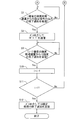
- FIG. 7 is a flowchart showing an ID setting process for the battery module processing unit by the battery ECU.
- FIG. 1 is a block diagram showing a configuration of a battery system according to an embodiment of the present invention.
- FIG. 2 is a block diagram showing the configuration of the arithmetic processing unit.
- FIG. 3 is a block diagram showing the configuration of the battery ECU.
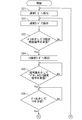
- FIG. 8 is a flowchart showing an ID setting process for the battery module processing unit by the battery ECU.
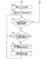
- FIG. 9 is a flowchart showing the operation of the arithmetic processing unit during the ID setting process.
- FIG. 10 is a flowchart showing the operation of the arithmetic processing unit during the ID setting process.
- FIG. 11 is an external perspective view showing an example of a battery module.
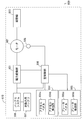
- FIG. 12 is a block diagram illustrating a configuration of an electric automobile including a battery system.
- FIG. 13 is a block diagram showing the configuration of the power supply apparatus.
- the battery system according to the present embodiment is mounted on an electric vehicle (for example, an electric automobile) that uses electric power as a drive source.
- the battery system can also be used for a power storage device or a consumer device including a plurality of battery cells that can be charged and discharged.
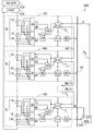
- FIG. 1 is a block diagram showing a configuration of a battery system according to an embodiment of the present invention.
- the battery system 500 includes a plurality of battery modules 100, a battery ECU (Electronic Control Unit) 510, a contactor 520, and an HV (High Voltage) connector 530.
- battery system 500 includes N battery modules 100. N is a natural number of 2 or more.
- Each battery module 100 includes a battery cell group BL including a plurality of battery cells 10, a voltage detection unit 20, an abnormality detection unit 30, an arithmetic processing unit 40, a switch circuit 50, a communication driver 60, and insulating elements DIa and DIb.
- the plurality of battery cells 10 in the battery cell group BL are connected in series.
- the battery cell group BL is disposed so as to be adjacent to each other and is integrally held as a battery block.
- a plurality of thermistors TH (see FIG. 11 described later) for detecting the temperature are attached to the battery cell group BL.
- Each battery cell 10 is a secondary battery such as a lithium ion battery or a nickel metal hydride battery.
- the battery cell groups BL of the plurality of battery modules 100 are connected in series through a power line. Thereby, in the battery system 500, all the battery cells 10 of the plurality of battery modules 100 are connected in series.
- the battery module 100 including the battery cell 10 having the lowest potential in FIG. 1 to the battery module 100 including the battery cell 10 having the highest potential is referred to as the first to Nth battery modules 100.
- the second to (N-2) th battery modules 100 are not shown.
- the arithmetic processing unit 40 of each battery module 100 is selectively set to a normal mode and an ID (identifier) setting mode. First, the operation of each part in the normal mode of each battery module 100 will be described.
- the voltage detection unit 20 detects the terminal voltages of the plurality of battery cells 10 and gives a detection signal DA indicating the detected terminal voltage value to the arithmetic processing unit 40.
- the abnormality detection unit 30 detects whether there is an abnormality in the terminal voltages of the plurality of battery cells 10 as an abnormality relating to charging / discharging of the corresponding battery cell group BL. In order to prevent overdischarge and overcharge of each battery cell 10, an allowable voltage range of the terminal voltage is determined.
- the abnormality detection unit 30 detects whether or not the terminal voltage of each battery cell 10 is equal to or higher than the upper limit value (hereinafter referred to as the upper limit voltage) of the allowable voltage range, and the terminal voltage is lower limit value (hereinafter referred to as the upper limit voltage range). , Referred to as the lower limit voltage).
- the abnormality detection unit 30 has a first duty ratio (for example, when the terminal voltage of at least one battery cell 10 of the corresponding battery cell group BL is equal to or higher than the upper limit voltage or equal to or lower than the lower limit voltage (when an abnormality is detected). 75%) is generated.
- the abnormality detection unit 30 has a second duty ratio (for example, 25%) when the terminal voltages of all the battery cells 10 in the corresponding battery cell group BL are within the allowable voltage range (when normal detection is performed).
- Generate DB The abnormality detection unit 30 gives the generated detection signal DB to the switch circuit 50. Further, the abnormality detection unit 30 outputs a status signal IC.
- the state signal IC becomes “H” level when the abnormality detection unit 30 operates. Thereby, the switch circuit 50 outputs the detection signal DB generated by the abnormality detection unit 30 to the insulating element DIb. It becomes “L” level when the abnormality detection unit 30 is stopped.
- the arithmetic processing unit 40 performs, for example, CAN (Controller Area Network) communication with the battery ECU 510 via the insulating element DIa and the communication driver 60. Thereby, the battery ECU 510 can easily perform broadcast communication with the N arithmetic processing devices 40.
- a communication system is configured by the N arithmetic processing units 40 and the battery ECU 510. In this case, battery ECU 510 serves as a master device, and arithmetic processing device 40 serves as a slave device.
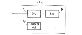
- FIG. 2 is a block diagram showing the configuration of the arithmetic processing unit 40.
- the arithmetic processing unit 40 includes a CPU (central processing unit) 41, a RAM (random access memory) 42, and a nonvolatile memory 43.
- the arithmetic processing unit 40 may be a microcomputer having functions of the CPU 41, the RAM 42, and the nonvolatile memory 43.
- the ID is stored in the RAM 42.
- the nonvolatile memory 43 stores the ID stored in the RAM 42.
- the operation of the CPU 41 will be described as the operation of the arithmetic processing unit 40.
- the arithmetic processing unit 40 transmits the terminal voltage values of the plurality of battery cells 10 to the battery ECU 510 based on the detection signal DA provided from the voltage detection unit 20. In addition, arithmetic processing unit 40 transmits to battery ECU 510 the temperature value of battery module 100 given from thermistor TH of FIG. Furthermore, the arithmetic processing unit 40 performs various arithmetic processes and determination processes using the terminal voltage values and temperature values of the plurality of battery cells 10. Further, arithmetic processing unit 40 receives various command signals from battery ECU 510 via bus BS and communication driver 60.
- the arithmetic processing unit 40 gives an ID setting signal IS to be described later to the switch circuit 50.
- the switch circuit 50 selectively outputs one of the detection signal DB provided from the abnormality detection unit 30 and the ID setting signal IS provided from the arithmetic processing unit 40 based on the state signal IC output from the abnormality detection unit 30. .
- the switch circuit 50 outputs the detection signal DB given from the abnormality detection unit 30 to the insulating element DIb.
- the switch circuit 50 outputs an ID setting signal IS given from the arithmetic processing unit 40 to the insulating element DIb.
- Battery ECU510 is connected to the insulating element DIb the N-th battery module 100 via the signal line P 0.
- Insulating element DIb the N-th battery module 100 is connected via a signal line P n and (N-1) -th insulating element DIb.
- the insulating element DIb of the (N ⁇ 1) th battery module 100 is connected to the (N ⁇ 2) th insulating element DIb via the signal line P n ⁇ 1 .
- insulating element DIb the second battery module 100 through the signal line P 2 is connected to the first insulating element DIb.
- Insulating element DIb the first battery module 100 is connected to the battery ECU510 via the signal line P 1.
- the battery ECU 510 and the first to Nth battery modules 100 are connected by the signal lines P 0 to P n .
- the signal line P 0 is not used.
- the detection signal DB generated by the abnormality detection unit 30 of the Nth battery module 100 is the insulation of the switch circuit 50, the insulation element DIb, the signal line Pn, and the (N ⁇ 1) th battery module 100. This is given to the abnormality detection unit 30 of the (N ⁇ 1) th battery module 100 via the element DIb.
- the detection signal DB generated by the abnormality detection unit 30 of the (N ⁇ 1) th battery module 100 is the switch circuit 50, the insulating element DIb, the signal line P n ⁇ 1 and the (N ⁇ 2) th battery module 100. This is supplied to the abnormality detection unit 30 of the (N ⁇ 2) th battery module 100 via the insulating element DIb.
- the detection signal DB generated by the second abnormality detecting unit 30 of the battery module 100, the switch circuit 50, insulation element DIb, via an insulating element DIb signal lines P 2 and the first battery module 100 1 The abnormality detection unit 30 of the second battery module 100 is provided. Detection signal DB generated by the abnormality detecting unit 30 of the first battery module 100, the switching circuit 50 is given to the battery ECU510 via an insulating element DIb and the signal line P 1.
- FIG. 3 is a block diagram showing the configuration of the battery ECU 510.
- battery ECU 510 includes an MPU (microprocessor) 511 and a memory 512.
- the memory 512 stores a program in the normal mode and a program in the ID setting mode.
- the MPU 511 operates according to a program stored in the memory 512.
- the operation of MPU 511 will be described as the operation of battery ECU 510.
- the battery ECU 510 calculates the charge amount of each battery cell 10 based on the terminal voltage values of the plurality of battery cells 10 given from the arithmetic processing unit 40 of the battery module 100. Also, the battery ECU 510 determines whether there is an abnormality related to charging / discharging of the battery cell group BL of each battery module 100 based on the terminal voltage values and temperatures of the plurality of battery cells 10 given from the arithmetic processing unit 40 of each battery module 100. Determine.
- the abnormality related to charging / discharging of the battery cell group BL of the battery module 100 includes, for example, current flowing through the battery cell group BL, terminal voltage of the battery cell 10, SOC (charge amount), overdischarge, overcharge, temperature abnormality, etc. Including.
- the battery ECU 510 detects the presence / absence of abnormality in the terminal voltages of the plurality of battery cells 10 of the battery module 100 based on the detection signal DB given from the first battery module 100.
- the power supply line connected to the highest potential positive electrode of the Nth battery module 100 and the power supply line connected to the lowest potential negative electrode of the first battery module 100 are connected to the contactor 520.
- Contactor 520 is connected to a load such as a motor of an electric vehicle via HV connector 530.
- the battery ECU 510 turns off the contactor 520 when an abnormality occurs in the battery module 100. Thereby, when an abnormality occurs, no current flows through the plurality of battery cells 10, so that abnormal heat generation of the battery module 100 is prevented.
- Battery ECU 510 is connected to main controller 300 (see FIG. 12 described later) of the electric vehicle via a bus.
- a charge amount of each battery module 100 (a charge amount of the battery cell 10) is given from the battery ECU 510 to the main control unit 300.
- the main control unit 300 controls the power of the electric vehicle (for example, the rotational speed of the motor) based on the amount of charge.
- the main control unit 300 controls each power generation device (not shown) connected to the power line to charge each battery module 100.
- FIG. 4 is a block diagram illustrating the configuration of the voltage detection unit 20 and the abnormality detection unit 30.
- the voltage detection unit 20 includes, for example, an ASIC (Application Specific Integrated Circuit).
- the voltage detection unit 20 includes a plurality of differential amplifiers 21, a multiplexer 22, an A / D (analog / digital) converter 23, and a communication circuit 24.
- FIG. 4 does not show a signal output circuit that outputs the state signal IC of FIG.
- Each differential amplifier 21 has two input terminals and an output terminal. Each differential amplifier 21 differentially amplifies the voltage input to the two input terminals, and outputs the amplified voltage from the output terminal. Two input terminals of each differential amplifier 21 are connected to a plus electrode and a minus electrode of the corresponding battery cell 10 by a conductor line W1, respectively. As a result, the voltage between the positive electrode and the negative electrode of each battery cell 10 is differentially amplified by each differential amplifier 21. The output voltage of each differential amplifier 21 corresponds to the terminal voltage of each battery cell 10. Terminal voltages output from the plurality of differential amplifiers 21 are supplied to the multiplexer 22. The multiplexer 22 sequentially outputs terminal voltages supplied from the plurality of differential amplifiers 21 to the A / D converter 23.
- the A / D converter 23 converts the terminal voltage output from the multiplexer 22 into a digital value.
- the digital value obtained by the A / D converter 23 is given to the arithmetic processing unit 40 (see FIG. 1) through the communication circuit 24 as a detection signal DA indicating the value of the terminal voltage.
- the abnormality detection unit 30 is made of, for example, an ASIC.
- the abnormality detection unit 30 includes a plurality of differential amplifiers 31, a multiplexer 32, a switch circuit 33, reference voltage output units 34 and 35, a comparator 36, a detection signal output circuit 37, and communication circuits 38a and 38b.
- Each differential amplifier 31 has two input terminals and an output terminal. Each differential amplifier 31 differentially amplifies the voltage input to the two input terminals, and outputs the amplified voltage from the output terminal.
- the two input terminals of each differential amplifier 31 are connected to the plus electrode and the minus electrode of the corresponding battery cell 10 by the conductor line W1, respectively.
- the output voltage of each differential amplifier 31 corresponds to the terminal voltage of each battery cell 10. Terminal voltages output from the plurality of differential amplifiers 31 are applied to the multiplexer 32.
- the multiplexer 32 sequentially outputs the terminal voltages supplied from the plurality of differential amplifiers 31 to the comparator 36.
- the switch circuit 33 has terminals CP0, CP1 and CP2.
- the reference voltage output unit 34 outputs the upper limit voltage Vth_O to the terminal CP1 of the switch circuit 33.
- the reference voltage output unit 35 outputs the lower limit voltage Vth_U to the output terminal CP2.
- the upper limit voltage Vth_O is set to, for example, 4.2V (4.19V to 4.21V)
- the lower limit voltage Vth_U is set to, for example, about 2.0V (1.99V to 2.01V).
- the comparator 36 has two input terminals and an output terminal. One input terminal of the comparator 36 is connected to the multiplexer 32. The other input terminal of the comparator 36 is connected to the terminal CP0 of the switch circuit 33. The switch circuit 33 is switched so that the terminal CP0 is alternately connected to the plurality of terminals CP1 and CP2 at a constant cycle. Thereby, the terminal voltage output from the multiplexer 32 is given to one input terminal of the comparator 36, and the upper limit voltage Vth_O and the lower limit voltage Vth_U are alternately given to the other input terminal of the comparator 36.
- the comparator 36 sequentially compares the terminal voltage of the battery cell 10 supplied from the multiplexer 32 with the upper limit voltage Vth_O and the lower limit voltage Vth_U, and outputs a signal indicating the comparison result to the detection signal output circuit 37.
- the detection signal output circuit 37 determines whether or not at least one terminal voltage of the plurality of battery cells 10 is equal to or higher than the upper limit voltage Vth_O based on the output signal of the comparator 36 and at least one of the plurality of battery cells 10. It is determined whether or not two terminal voltages are lower than the lower limit voltage Vth_U.
- the detection signal output circuit 37 determines that the terminal voltage of the corresponding battery cell group BL is abnormal. .
- the detection signal output circuit 37 determines that the terminal voltage of the corresponding battery cell group BL is normal.
- the detection signal output circuit 37 When it is determined that the terminal voltage of the corresponding battery cell group BL is abnormal, the detection signal output circuit 37 generates a detection signal DB having a first duty ratio (for example, 75%). When the detection signal output circuit 37 determines that the terminal voltage of the corresponding battery cell group BL is normal, the detection signal output circuit 37 generates the detection signal DB having the second duty ratio (for example, 25%). Communication circuit 38b provides a detection signal DB generated by the detection signal output circuit 37 switching circuit 50, the abnormality detecting portion 30 of the insulating element via DIb and the signal line P n (N-1) th battery module 100 .
- the configuration of the voltage detector 20 and the abnormality detector 30 of the i-th battery module 100 (i is an arbitrary natural number from 2 to (N ⁇ 1)) is the voltage detection of the N-th battery module 100 except for the following points.
- the configuration and operation of the unit 20 and the abnormality detection unit 30 are the same.
- the communication circuit 38 a supplies the detection signal DB supplied from the (i + 1) -th battery module 100 to the detection signal output circuit 37.
- the detection signal output circuit 37 determines that the terminal voltage of the corresponding battery cell group BL is abnormal or when the detection signal supplied from the communication circuit 38a has the first duty ratio (for example, 75%), A detection signal DB having a duty ratio of 1 (for example, 75%) is generated.
- the detection signal output circuit 37 determines that the terminal voltage of the corresponding battery cell group BL is normal and the detection signal provided from the communication circuit 38a has the second duty ratio (for example, 25%)
- the detection signal DB having a duty ratio for example, 25%
- the communication circuit 38 b gives the detection signal DB generated by the detection signal output circuit 37 to the (i ⁇ 1) th battery module 100.
- the configurations of the voltage detection unit 20 and the abnormality detection unit 30 of the first battery module 100 are the same as the configurations and operations of the voltage detection unit 20 and the abnormality detection unit 30 of the i-th battery module 100 except for the following points.
- the communication circuit 38b is a detection signal DB generated by the detection signal output circuit 37 via the signal line P 1 applied to the battery ECU 510.
- the battery ECU 510 acquires the detection signal DB having the first duty ratio (for example, 75%) from the first battery module 100. To do.
- the battery ECU 510 detects from the first battery module 100 a detection signal having a second duty ratio (for example, 25%). Get DB. Thereby, the battery ECU 510 can detect the presence or absence of abnormality in the terminal voltages of the plurality of battery cells 10 of the battery module 100.
- Each battery module 100 may include a plurality of voltage detection units 20 and a plurality of abnormality detection units 30 connected in series.
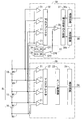
- FIG. 5 is a block diagram showing a configuration when each battery module 100 includes a plurality of voltage detection units 20 and a plurality of abnormality detection units 30.
- FIG. 5 shows the configuration of the battery module 100.
- the battery module 100 includes three voltage detection units 20 and three abnormality detection units 30.
- One voltage detection unit 20 (hereinafter, referred to as a low potential voltage detection unit 20L) includes one third of the plurality of battery cells 10 on the low potential side (hereinafter referred to as a low potential battery cell group 10L). It corresponds to).
- the other voltage detectors 20 (hereinafter referred to as medium potential voltage detectors 20M) have a number of battery cells 10 (hereinafter, referred to as medium potential battery cell group 10M) of the middle potential among the plurality of battery cells 10.
- another voltage detection unit 20 (hereinafter, referred to as a high potential voltage detection unit 20H) has a number of battery cells 10 (six in this example) that are 1/3 of the plurality of battery cells 10 on the high potential side (in this example). Hereinafter, it is referred to as a high potential battery cell group 10H.
- the low potential voltage detector 20L detects the terminal voltages of the plurality of battery cells 10 in the low potential battery cell group 10L.
- the medium potential voltage detection unit 20M detects terminal voltages of the plurality of battery cells 10 in the medium potential battery cell group 10M.
- the high potential voltage detector 20H detects the terminal voltages of the plurality of battery cells 10 in the high potential battery cell group 10H.
- the detection signal DA output from the communication circuit 24 (see FIG. 4) of the high potential voltage detection unit 20H is communicated with the low potential voltage detection unit 20L via the communication circuit 24 (see FIG. 4) of the medium potential voltage detection unit 20M. It is given to the circuit 24 (see FIG. 4), and is given to the arithmetic processing unit 40 from the communication circuit 24 of the low potential voltage detector 20L.
- the detection signal DA output from the communication circuit 24 of the medium potential voltage detection unit 20M is supplied to the communication circuit 24 of the low potential voltage detection unit 20L, and is supplied from the communication circuit 24 of the low potential voltage detection unit 20L to the arithmetic processing unit 40. .
- the detection signal DA output from the communication circuit 24 of the low potential voltage detection unit 20L is given to the arithmetic processing unit 40.
- One abnormality detection unit 30 (hereinafter referred to as a low potential abnormality detection unit 30L) corresponds to the low potential battery cell group 10L.
- Other abnormality detection unit 30 (hereinafter referred to as medium potential abnormality detection unit 30M) corresponds to medium potential battery cell group 10M.
- Still another abnormality detection unit 30 (hereinafter referred to as a high potential abnormality detection unit 30H) corresponds to the high potential battery cell group 10H.
- the low potential abnormality detection unit 30L detects the presence or absence of abnormality of the plurality of battery cells 10 in the low potential battery cell group 10L.
- the medium potential abnormality detection unit 30M detects the presence or absence of abnormality of the plurality of battery cells 10 in the medium potential battery cell group 10M.
- the high potential abnormality detection unit 30H detects the presence or absence of abnormality of the plurality of battery cells 10 in the high potential battery cell group 10H.
- the communication circuit 38b (see FIG. 4) of the high potential abnormality detection unit 30H and the communication circuit 38a (see FIG. 4) of the medium potential abnormality detection unit 30M are connected.
- the communication circuit 38b (see FIG. 4) of the medium potential abnormality detection unit 30M is connected to the communication circuit 38a (see FIG. 4) of the low potential abnormality detection unit 30L.
- the communication circuit 38b (see FIG. 4) of the low potential abnormality detection unit 30L is connected to the switch circuit 50 (see FIG. 1).
- the high potential abnormality detection unit 30H of the i-th battery module 100 (i is a natural number of 2 to (N ⁇ 1)) includes the abnormality detection unit 30 (low potential abnormality detection unit 30L) of the (i + 1) th battery module 100.
- the detection signal output circuit 37 determines that the terminal voltage of the corresponding high potential battery cell group 10H is abnormal or the communication circuit 38a.
- the detection signal output circuit 37 determines that the terminal voltage of the corresponding high-potential battery cell group 10H is normal, and is given a detection signal DB having a second duty ratio (for example, 25%) by the communication circuit 38a.
- the detection signal DBH having the second duty ratio (for example, 25%) is generated.
- the communication circuit 38b (see FIG. 4) provides the detection signal DBH generated by the detection signal output circuit 37 to the medium potential abnormality detection unit 30M.
- the communication circuit 38a gives the detection signal DBH given by the high potential abnormality detection unit 30H to the detection signal output circuit 37 (see FIG. 4).
- the detection signal output circuit 37 is supplied with the detection signal DBH having the first duty ratio (for example, 75%) when it is determined that the terminal voltage of the corresponding medium potential battery cell group 10M is abnormal or by the communication circuit 38a. In this case, a detection signal DBM having a first duty ratio (for example, 75%) is generated.
- the detection signal output circuit 37 determines that the terminal voltage of the corresponding medium potential battery cell group 10M is normal, and is provided with the detection signal DBH having the second duty ratio (for example, 25%) by the communication circuit 38a.
- the detection signal DBM having the second duty ratio (for example, 25%) is generated.
- the communication circuit 38b supplies the detection signal DBM generated by the detection signal output circuit 37 to the low potential abnormality detection unit 30L.
- the communication circuit 38a gives the detection signal DBM given by the medium potential abnormality detection unit 30M to the detection signal output circuit 37 (see FIG. 4).
- the detection signal output circuit 37 determines that the terminal voltage of the corresponding low-potential battery cell group 10L is abnormal or the communication circuit 38a gives the detection signal DBM having the first duty ratio (for example, 75%).
- a detection signal DBL having a first duty ratio for example, 75%) is generated.
- the detection signal output circuit 37 determines that the terminal voltage of the corresponding low-potential battery cell group 10L is normal, and is given a detection signal DBM having a first duty ratio (for example, 75%) by the communication circuit 38a.
- a detection signal DBL of “L” level indicating normality is generated.
- the communication circuit 38b uses the detection signal DBL generated by the detection signal output circuit 37 as the detection signal DB, and detects the abnormality detection unit 30 (high potential abnormality detection unit 30H) of the (i-1) th battery module 100. To give.
- the operation of the abnormality detection unit 30 of the Nth battery module 100 is the same as the operation of the abnormality detection unit 30 of the i-th battery module 100 except for the following points.
- the detection signal DB is not supplied to the communication circuit 38a of the high potential abnormality detection unit 30H of the Nth battery module 100. Therefore, in the high potential abnormality detection unit 30H of the Nth battery module 100, when the detection signal output circuit 37 (see FIG. 4) determines that the terminal voltage of the corresponding high potential battery cell group 10H is abnormal, A detection signal DBH having a first duty ratio (for example, 75%) is generated. Further, when the detection signal output circuit 37 determines that the terminal voltage of the corresponding high potential battery cell group 10H is normal, the detection signal output circuit 37 generates a detection signal DBH having a second duty ratio (for example, 25%).
- the operation of the abnormality detection unit 30 of the first battery module 100 is the same as the operation of the abnormality detection unit 30 of the i-th battery module 100 except for the following points.
- the communication circuit 38b (see FIG. 4) of the abnormality detection unit 30 of the first battery module 100 supplies the detection signal DBL generated by the detection signal output circuit 37 to the battery ECU 510 as the detection signal DB.
- FIG. 6 is a schematic plan view illustrating a configuration example of the printed circuit board of the battery module 100.
- the printed circuit board 110 includes a first mounting region MT1, a second mounting region MT2, and a strip-shaped insulating region INS.
- the second mounting region MT2 is formed at one corner of the printed circuit board 110.
- the insulating region INS is formed to extend along the second mounting region MT2.
- the first mounting region MT1 is formed in the remaining part of the printed circuit board 110.
- the first mounting region MT1 and the second mounting region MT2 are separated from each other by the insulating region INS. Thereby, the first mounting region MT1 and the second mounting region MT2 are electrically insulated by the insulating region INS.
- the voltage detection unit 20, the abnormality detection unit 30, the arithmetic processing unit 40, and the switch circuit 50 are mounted.
- the plurality of battery cells 10 of the battery cell group BL include the voltage detection unit 20, the abnormality detection unit 30, the arithmetic processing unit 40, and the switch circuit 50.
- the ground pattern GND1 is formed in the first mounting region MT1 except for the mounting region of the voltage detection unit 20, the abnormality detection unit 30, the arithmetic processing unit 40 and the switch circuit 50 and the connection line formation region.
- the ground pattern GND1 is held at the reference potential (ground potential) of the plurality of battery cells 10 in the battery cell group BL.
- the communication driver 60 and the connectors CNa to CNc are mounted.
- a non-power battery BAT of the electric vehicle is connected to the communication driver 60 as a power source for the communication driver 60.
- the ground pattern GND2 is formed in the second mounting area MT2 except for the mounting area of the communication driver 60 and the connectors CNa to CNc and the formation area of a plurality of connection lines.
- the ground pattern GND2 is held at the reference potential (ground potential) of the non-power battery BAT.
- the communication driver 60 can be stably operated independently from the voltage detection unit 20, the abnormality detection unit 30, the arithmetic processing unit 40, and the switch circuit 50.
- the insulating element DIa is mounted so as to straddle the insulating region INS.
- the insulating element DIa transmits a signal between the voltage detection unit 20 and the arithmetic processing device 40 while electrically insulating the arithmetic processing device 40 and the communication driver 60 from each other.
- the insulating element DIb is mounted so as to straddle the insulating region INS.
- the insulating element DIb transmits a signal between the switch circuit 50 and the connector CNb while electrically insulating the switch circuit 50 and the connector CNb from each other.
- the insulating element DIb transmits a signal between the communication circuit 38a of the abnormality detection unit 30 and the connector CNc while electrically insulating the communication circuit 38a (see FIG.
- the insulating element DIb transmits a signal between the arithmetic processing unit 40 and the connector CNc while electrically insulating the arithmetic processing unit 40 and the connector CNc from each other.
- the insulating elements DIa and DIb for example, digital isolators or photocouplers can be used. In the present embodiment, digital isolators are used as the insulating elements DIa and DIb.
- Communication driver 60 and connector CNa are connected. Thereby, the value of the terminal voltage of the plurality of battery cells 10 and the value of the temperature of the battery module 100 output from the arithmetic processing unit 40 are given to the connector CNa.
- the bus BS in FIG. 1 is connected to the connector CNa.
- Connector CNc of the N-th battery module 100 is connected to the battery ECU510 via signal lines P 0.
- N-th connector CNb of the battery module 100 is connected via a signal line P n and (N-1) th battery module 100 of the connector CNc.
- the connector CNb of the (N ⁇ 1) th battery module 100 is connected to the connector CNc of the (N ⁇ 2) th battery module 100 via the signal line P n ⁇ 1 .
- the second connector CNb of the battery module 100 via the signal line P 2 is connected to the first battery module 100 connector CNc.
- the first connector CNb of the battery module 100 is connected to the battery ECU510 via the signal line P 1.
- the arithmetic processing unit 40 of the battery module 100 shifts to the ID setting mode by receiving an ID setting start signal indicating the start of the ID setting process from the battery ECU 510 via the bus BS. The operation of each unit in the ID setting mode of each battery module 100 will be described.
- the arithmetic processing unit 40 stops the function of the abnormality detection unit 30. In this case, the status signal IC output from the abnormality detection unit 30 becomes “L” level. Thereby, the switch circuit 50 is switched to a state in which the ID setting signal IS given by the arithmetic processing unit 40 can be output.
- the ID setting signal IS generated by the battery ECU 510 is given to the arithmetic processing unit 40 of the Nth battery module 100 via the signal line P 0 and the insulating element DIb of the Nth battery module 100. It is done.
- the ID setting signal IS generated by the arithmetic processing unit 40 of the (N-1) th battery module 100 includes the switch circuit 50, the insulating element DIb, the signal line Pn-1, and the (N-2) th battery module 100. Is supplied to the arithmetic processing unit 40 of the (N ⁇ 2) th battery module 100 through the insulating element DIb.
- the second battery module 100 ID setting signal is generated by the processor 40 of the IS, the switch circuit 50, insulation element DIb, via an insulating element DIb signal lines P 2 and the first battery module 100 This is given to the arithmetic processing unit 40 of the first battery module 100.
- the signal line P 1 is not used.
- Each arithmetic processing unit 40 can only receive messages such as various signals, commands, and notifications from the battery ECU 510 through the bus BS when no ID is set. Further, after the ID is set, each arithmetic processing unit 40 can transmit and receive messages such as various signals, commands, and notifications from the battery ECU 510 through the bus BS.
- ID setting process The ID setting process with respect to the arithmetic processing unit 40 of the battery module 100 by the battery ECU 510 will be described.
- 7 and 8 are flowcharts showing an ID setting process for the arithmetic processing unit 40 of the battery module 100 by the battery ECU 510.
- FIG. Hereinafter, the arithmetic processing devices 40 of the first to Nth battery modules 100 are referred to as the first to Nth arithmetic processing devices 40, respectively.
- the battery ECU 510 transmits an ID setting start signal indicating the start of the ID setting process to the first to Nth arithmetic processing devices 40 via the bus BS by broadcast communication (step S1).
- the arithmetic processing device 40 stops the operation of the voltage detection unit 20 and the abnormality detection unit 30.
- the status signal IC output from the abnormality detection unit 30 becomes “L” level.
- the switch circuit 50 is switched to a state in which the ID setting signal IS output from the arithmetic processing unit 40 can be selectively output.
- the battery ECU 510 outputs an “H” level N-th ID setting signal IS to the N-th arithmetic processing unit 40 via the signal line P 0 (step S2). Thereby, the Nth arithmetic processing unit 40 is instructed to set the ID. Subsequently, battery ECU 510 transmits ID “N” via bus BS (step S3). As a result, the Nth arithmetic processing unit 40 receives the ID “N” via the bus BS.
- the Nth arithmetic processing unit 40 stores the received ID “N” in the RAM 42 (see FIG. 2). As a result, the ID “N” is set in the Nth arithmetic processing unit 40. As a result, the Nth arithmetic processing unit 40 can send and receive messages to and from the battery ECU 510 through the bus BS. The Nth arithmetic processing unit 40 transmits an ID setting completion notification to the battery ECU 510 via the bus BS.
- the battery ECU 510 waits until receiving an ID setting completion notification from the Nth arithmetic processing unit 40 (step S4).
- the battery ECU 510 sets the value of the variable i (natural number from 2 to N) to “N” (step S5).
- the battery ECU 510 instructs the i-th arithmetic processing unit 40 to output the (i ⁇ 1) -th ID setting signal IS at the “H” level via the bus BS. (Step S6).
- the i-th arithmetic processing unit 40 When an instruction to output the (i ⁇ 1) -th ID setting signal IS of “H” level is received from the battery ECU 510 via the bus BS, the i-th arithmetic processing unit 40 receives (i ⁇ 1) of “H” level. The first ID setting signal IS is output. Thereafter, the i-th arithmetic processing unit 40 transmits an output completion notification of the (i ⁇ 1) -th ID setting signal IS to the battery ECU 510 via the bus BS. The (i ⁇ 1) th ID setting signal IS of “H” level output from the i-th arithmetic processing unit 40 is given to the (i ⁇ 1) th arithmetic processing unit 40 via a signal line. Thereby, the (i ⁇ 1) th arithmetic processing unit 40 is instructed to set the ID.
- the battery ECU 510 waits until receiving the completion notification of the output of the (i-1) th ID setting signal IS from the i-th arithmetic processing unit 40 (step S7). Upon receiving the completion notification of the output of the (i ⁇ 1) th ID setting signal IS from the ith arithmetic processing unit 40, the battery ECU 510 transmits the ID “i ⁇ 1” via the bus BS (step S8). . As a result, the (i ⁇ 1) th arithmetic processing unit 40 receives the ID “i ⁇ 1” via the bus BS.
- the (i ⁇ 1) -th arithmetic processing unit 40 stores the received ID “i ⁇ 1” in the RAM 42 (see FIG. 2). As a result, the ID “i ⁇ 1” is set to the (i ⁇ 1) th arithmetic processing unit 40. As a result, the (i-1) th arithmetic processing unit 40 can transmit and receive messages to and from the battery ECU 510 through the bus BS. The (i-1) th arithmetic processing unit 40 transmits an ID setting completion notification to the battery ECU 510 via the bus BS.
- the battery ECU 510 waits until an ID setting completion notification is received from the (i-1) th arithmetic processing unit 40 (step S9).
- the battery ECU 510 updates the value of the variable i to “i ⁇ 1” (step S10).
- battery ECU 510 determines whether or not the value of variable i is 1 (step S11).
- Step S6 to S11 are repeated until the value of variable i becomes 1. Accordingly, the (N ⁇ 1) th to first arithmetic processing devices 40 store IDs “N ⁇ 1” to “1” in the RAM 42 (see FIG. 2), respectively. As a result, IDs “N ⁇ 1” to “1” are set in the (N ⁇ 1) th to first arithmetic processing units 40, respectively.
- the battery ECU 510 transmits an ID setting process end notification to the first to Nth arithmetic processing devices 40 via the bus BS (step S12). Thereby, all the arithmetic processing units 40 shift from the ID setting mode to the normal mode.
- the arithmetic processing unit 40 shifts to the normal mode when activated (step S21), and operates in the normal mode (step S22). In addition, arithmetic processing unit 40 determines whether or not an ID setting start signal has been received from battery ECU 510 via bus BS (step S23). When the ID setting start signal is not received, the arithmetic processing unit 40 returns to the process of step S22 and performs the operation in the normal mode.
- the processing unit 40 shifts to the ID setting mode (step S24). Thereafter, the processing unit 40 stands by until it receives the i-th ID setting signal IS of “H” level via the signal line (step S25). When the i-th ID setting signal IS of “H” level is received, the arithmetic processing unit 40 is instructed to set the ID. In this case, arithmetic processing unit 40 stands by until an ID is received from battery ECU 510 via bus BS (step S26).
- the arithmetic processing unit 40 stores the received ID in the RAM 42 (see FIG. 2) (step S27). Thereby, the ID is set in the arithmetic processing unit 40. As a result, the arithmetic processing unit 40 can send and receive messages to and from the battery ECU 510 through the bus BS. In this case, arithmetic processing unit 40 transmits an ID setting completion notification to battery ECU 510 via bus BS (step S28).
- the processing unit 40 determines whether or not an ID setting process end notification is received from the battery ECU 510 via the bus BS (step S29). If the ID setting process end notification has not been received, the arithmetic processing unit 40 has received an instruction to output the (i ⁇ 1) th ID setting signal IS at the “H” level from the battery ECU 510 via the bus BS. Is determined (step S30).
- the arithmetic processing unit 40 If the instruction to output the (i-1) th ID setting signal IS at the “H” level has not been received, the arithmetic processing unit 40 returns to the process of step S29.
- the arithmetic processing unit 40 sets the (i ⁇ 1) th ID setting at the “H” level via the signal line.
- the signal IS is output to the (i ⁇ 1) th arithmetic processing unit 40 (step S31).
- the arithmetic processing unit 40 transmits a completion notification of the output of the (i ⁇ 1) th ID setting signal IS to the battery ECU 510 via the bus BS (step S32). Thereafter, the arithmetic processing unit 40 returns to the process of step S29.
- step S29 when the notification of completion of the ID setting process is received, the arithmetic processing unit 40 saves the ID stored in the RAM 42 (see FIG. 2) in the nonvolatile memory 43 (see FIG. 2), and performs the process in step S21. Return. Thereby, all the arithmetic processing units 40 shift from the ID setting mode to the normal mode. Thereafter, by repeating the processes of steps S22 and S23, the arithmetic processing unit 40 operates in the normal mode.
- FIG. 11 is an external perspective view showing an example of the battery module 100.
- three directions orthogonal to each other are defined as an X direction, a Y direction, and a Z direction.
- the X direction and the Y direction are directions parallel to the horizontal plane
- the Z direction is a direction orthogonal to the horizontal plane.
- the upward direction is the direction in which the arrow Z faces.
- a plurality of battery cells 10 having a flat, substantially rectangular parallelepiped shape are arranged so as to be arranged in the X direction.
- a pair of end face frames EP having a substantially plate shape are arranged in parallel to the YZ plane.
- the pair of upper end frames FR1 and the pair of lower end frames FR2 are arranged to extend in the X direction.
- connection portions for connecting the pair of upper end frames FR1 and the pair of lower end frames FR2 are formed.
- the pair of upper end frames FR1 are attached to the upper connection portions of the pair of end surface frames EP, and the lower connection of the pair of end surface frames EP
- a pair of lower end frames FR2 are attached to the part.
- the plurality of battery cells 10 are integrally fixed by the pair of end surface frames EP, the pair of upper end frames FR1, and the pair of lower end frames FR2.
- the plurality of battery cells 10, the pair of end face frames EP, the pair of upper end frames FR1, and the pair of lower end frames FR2 constitute a substantially rectangular parallelepiped battery block BLK.
- the battery block BLK includes the battery cell group BL of FIG.
- the printed circuit board 110 is attached to one end face frame EP.
- a plurality of thermistors TH for detecting the temperature of the battery module 100 are attached to the side surface of the battery block BLK.
- each battery cell 10 has a plus electrode 10a and a minus electrode 10b on the upper surface of the battery block BLK so as to be arranged in the Y direction.
- each battery cell 10 is arranged such that the positional relationship between the plus electrode 10 a and the minus electrode 10 b in the Y direction is opposite between adjacent battery cells 10.
- one electrode 10a, 10b of the plurality of battery cells 10 is arranged in a line along the X direction
- the other electrode 10a, 10b of the plurality of battery cells 10 is arranged in a line along the X direction.
- the plus electrode 10a of one battery cell 10 and the minus electrode 10b of the other battery cell 10 are close to each other, and the minus electrode 10b of one battery cell 10 and the other electrode are The positive electrode 10a of the battery cell 10 is in close proximity.
- a bus bar BB made of, for example, copper is attached to the two adjacent electrodes 10a and 10b.
- the some battery cell 10 is connected in series.
- a long flexible printed circuit board (hereinafter abbreviated as an FPC board) 120 extending in the X direction is commonly connected to the plurality of bus bars BB on one end side of the plurality of battery cells 10 in the Y direction.
- a long FPC board 120 extending in the X direction is commonly connected to the plurality of bus bars BB on the other end side of the plurality of battery cells 10 in the Y direction.
- the FPC board 120 has a configuration in which a plurality of conductor wires W1 shown in FIG. 4 to be described later are mainly formed on an insulating layer, and has flexibility and flexibility.
- polyimide is used as the material of the insulating layer constituting the FPC board 120
- copper is used as the material of the conductor wire W1.
- Each FPC board 120 is folded at a right angle toward the inside at the upper end portion of one end face frame EP of the battery block BLK, is further folded downward, and is connected to the printed circuit board 110. Thereby, the voltage detection unit 20 and the abnormality detection unit 30 of FIG. 1 are connected to the positive electrode 10a and the negative electrode 10b of the battery cell 10.
- the battery ECU 510 that is the master device and the control device is connected to the arithmetic processing device 40 that is the processing device of the first to Nth battery modules 100 and the communication line.
- the arithmetic processing devices 40 of the first to Nth battery modules 100 are the first to Nth arithmetic processing devices 40, respectively.
- the battery ECU 510 outputs an ID setting signal IS that is an Nth setting signal that instructs the Nth arithmetic processing unit 40 to set an ID that is an identifier, and transmits the ID of the Nth arithmetic processing unit 40 to the bus BS. To do.
- the Nth arithmetic processing unit 40 stores the ID of the Nth arithmetic processing unit 40 transmitted by the battery ECU 510 when receiving the Nth ID setting signal IS. Thereby, the ID of the Nth arithmetic processing device 40 transmitted by the battery ECU 510 is set in the Nth arithmetic processing device 40.
- battery ECU 510 can transmit a command to Nth arithmetic processing device 40 using the ID, and Nth arithmetic processing device 40 can receive a command from battery ECU510.
- the battery ECU 510 causes the i th (i is a natural number from N to 2) arithmetic processing unit 40 to output the (i ⁇ 1) th ID setting signal IS to the (i ⁇ 1) th arithmetic processing unit 40.
- the i-th processing unit 40 is commanded and the ID of the (i-1) -th processing unit 40 is transmitted to the bus BS.
- the i-th arithmetic processing unit 40 responds to the output command of the (i-1) -th ID setting signal IS to the (i-1) -th arithmetic processing unit 40.
- the setting signal IS is output.
- the (i-1) th arithmetic processing unit 40 stores the ID of the (i-1) th arithmetic processing unit 40 transmitted by the battery ECU 510 when receiving the (i-1) th ID setting signal IS. Then, such an operation is performed in order from the Nth to the second arithmetic processing unit 40.
- the battery ECU 510 sends the Nth arithmetic processing unit 40 to the Nth arithmetic processing unit 40 so that the (N-1) th arithmetic processing unit 40 outputs the (N-1) th ID setting signal IS.
- the ID of the (N-1) th arithmetic processing unit 40 is transmitted to the bus BS.
- the Nth arithmetic processing unit 40 responds to the output command of the (N-1) th ID setting signal IS to the (N-1) th arithmetic processing unit 40.
- the setting signal IS is output.
- the (N-1) th arithmetic processing unit 40 stores the ID of the (N-1) th arithmetic processing unit 40 transmitted by the battery ECU 510 when receiving the (N-1) th ID setting signal IS. To do.
- the battery ECU 510 outputs the (N ⁇ 2) th ID setting signal IS to the (N ⁇ 1) th arithmetic processing device 40 to the (N ⁇ 2) th arithmetic processing device 40 (N ⁇ ).
- 1) Command the first arithmetic processing unit 40 and send the ID of the (N-2) th arithmetic processing unit 40 to the bus BS.
- the (N-1) th arithmetic processing unit 40 responds to the output command of the (N-2) th ID setting signal IS to the (N-2) th arithmetic processing unit 40 (N-2).
- the first ID setting signal IS is output.
- the (N-2) th arithmetic processing unit 40 stores the ID of the (N-2) th arithmetic processing unit 40 transmitted by the battery ECU 510 when receiving the (N-2) th ID setting signal IS. To do.
- the battery ECU 510 (N ⁇ 2) outputs the (N ⁇ 3) th ID setting signal IS to the (N ⁇ 2) th arithmetic processing device 40 to the (N ⁇ 3) th arithmetic processing device 40 (N ⁇ ). 2) Instruct the first arithmetic processing unit 40 and transmit the ID of the (N-3) th arithmetic processing unit 40 to the bus BS.
- the (N-2) th arithmetic processing unit 40 responds to the command to output the (N-3) th ID setting signal IS to the (N-3) th arithmetic processing unit 40 (N-3).
- the first ID setting signal IS is output.
- the (N-3) th arithmetic processing unit 40 stores the ID of the (N-3) th arithmetic processing unit 40 transmitted by the battery ECU 510 when receiving the (N-3) th ID setting signal IS. To do.
- the battery ECU 510 instructs the third arithmetic processing unit 40 so that the third arithmetic processing unit 40 outputs the second ID setting signal IS to the second arithmetic processing unit 40 and 2
- the ID of the first arithmetic processing unit 40 is transmitted to the bus BS.
- the third arithmetic processing unit 40 outputs the second ID setting signal IS to the second arithmetic processing unit 40 in response to a command for outputting the second ID setting signal IS.
- the second arithmetic processing unit 40 stores the ID of the second arithmetic processing unit 40 transmitted by the battery ECU 510 when receiving the second ID setting signal IS.
- the battery ECU 510 instructs the second arithmetic processing unit 40 so that the second arithmetic processing unit 40 outputs the first ID setting signal IS to the first arithmetic processing unit 40 and the first arithmetic processing.
- the ID of the device 40 is transmitted to the bus BS.
- the second arithmetic processing unit 40 outputs the first ID setting signal IS to the first arithmetic processing unit 40 in response to an instruction to output the first ID setting signal IS.
- the IDs of the Nth to second arithmetic processing devices 40 transmitted by the battery ECU 510 are set in the Nth to second arithmetic processing devices 40, respectively.
- the first arithmetic processing unit 40 stores the ID of the first arithmetic processing unit 40 transmitted by the battery ECU 510 when receiving the first ID setting signal IS. Thereby, the ID of the first arithmetic processing unit 40 transmitted by the battery ECU 510 is set in the first arithmetic processing unit 40.
- the Nth to first ID setting signals IS are sequentially output from the battery ECU 510 and the Nth to second arithmetic processing devices 40 to the Nth to first arithmetic processing devices 40, and from the battery ECU 510 to the bus.
- the IDs of the Nth to first arithmetic processing units 40 are transmitted to the BS.
- the battery ECU 510 can recognize that an ID has been set for each arithmetic processing unit 40. Thereby, ID can be easily set to the plurality of arithmetic processing devices 40 while ensuring the reliability of communication between the battery ECU 510 and the plurality of arithmetic processing devices 40.
- the arithmetic processing unit 40 of each battery module 100 can reliably transmit the detection result of the voltage of each battery cell 10 of the battery cell group BL detected by the voltage detection unit 20 to the battery ECU 510.
- each battery module 100 the voltage detector 20 detects the terminal voltage of each battery cell 10 in the battery cell group BL.
- the arithmetic processing unit 40 of each battery module 100 can reliably transmit the terminal voltage value of each battery cell 10 of the battery cell group BL detected by the voltage detection unit 20 to the battery ECU 510.
- battery ECU 510 is CAN-connected to arithmetic processing unit 40 of a plurality of battery modules 100.
- the battery ECU 510 can be easily connected to the arithmetic processing unit 40 of the plurality of battery modules 100 so as to be able to perform broadcast communication.
- each of the plurality of battery modules 100 further includes an abnormality detection unit 30 that is an abnormality detection unit and a switch circuit 50 that is a selection unit.
- the abnormality detection unit 30 detects an abnormal state related to charging / discharging of the battery cell group BL, and generates a detection signal DB indicating the abnormal state.
- the switch circuit 50 selectively outputs one of the (i ⁇ 1) th ID setting signal IS output from the arithmetic processing unit 40 and the detection signal DB generated by the abnormality detection unit 30.
- Battery ECU510 is connected by a signal line P 0 is the first signal line to the N-th processing unit 40.
- the switch circuit 50 of the i-th battery module 100 is connected to the abnormality detection unit 30 and the arithmetic processing unit 40 of the (i ⁇ 1) -th battery module 100 through signal lines P n to P 2 that are second signal lines.
- the switch circuit 50 of the first battery module 100 is connected to the battery ECU510 by a signal line P 1 is the third signal line.
- the battery ECU510 In ID setting mode, the battery ECU510 outputs via the signal line P 0 to N-th ID setting signals IS to N-th processing unit 40.
- the switch circuit 50 of the i-th battery module 100 receives the (i ⁇ 1) -th ID setting signal IS output from the i-th arithmetic processing unit 40 via the signal lines P n to P 2 (i ⁇ 1). To the th processor 40.
- the switch circuit 50 of the i-th battery module 100 uses the detection signal DB generated by the i-th abnormality detection unit 30 to detect the (i ⁇ 1) -th abnormality via the signal lines P n to P 2. output to section 30, the switch circuit 50 of the first battery module 100 outputs a detection signal DB generated by the first abnormality detecting unit 30 via the signal line P 1 to the battery ECU 510.
- the battery ECU510 outputs via the signal line P 0 to N-th ID setting signals IS to N-th processing unit 40.
- the switch circuit 50 of the i-th battery module 100 receives the (i ⁇ 1) -th ID setting signal IS output from the i-th arithmetic processing unit 40 via the signal lines P n to P 2 (i ⁇ 1). To the th processor 40.
- the switch circuit 50 of the i-th battery module 100 uses the detection signal DB generated by the i-th abnormality detection unit 30 to detect the (i ⁇ 1) -th abnormality via the signal lines P n to P 2. To the unit 30.
- the switch circuit 50 of the first battery module 100 outputs a detection signal DB generated by the first abnormality detecting unit 30 via the signal line P 1 to the battery ECU 510.
- the signal lines P n to P 2 connecting the switch circuits 50 of the plurality of battery modules 100 output the (i ⁇ 1) th ID setting signal IS in the ID setting mode and the detection in the normal mode. Used in common for the output of the signal DB.
- the battery system 500 can have a function of detecting an abnormal state related to charging / discharging of the battery cell group BL without complicating the configuration and wiring of the battery system 500.
- the signal lines P n to P 2 connecting the switch circuits 50 of the battery module 100 are commonly used for the output of the ID setting signal IS in the ID setting mode and the output of the detection signal DB in the normal mode.
- the abnormality of the terminal voltage of the battery cell group BL detected by the abnormality detection unit 30 is detected by a plurality of switches.
- Battery ECU 510 can be notified via circuit 50, insulating element DIb, and signal lines P n to P 1 .
- the value of the terminal voltage of the battery cell group BL detected by the voltage detection unit 20 is calculated using the arithmetic processing unit 40, insulation
- the battery ECU 510 can be notified through the element DIa, the communication driver 60, and the bus BS. In this way, it is possible to reliably notify the battery ECU 510 of the occurrence of an abnormality in the terminal voltage of the battery cell group BL of the plurality of battery modules 100.
- Electric vehicle (1) Configuration and operation An electric vehicle will be described.
- the electric vehicle includes the battery system 500 according to the above embodiment.
- an electric vehicle will be described as an example of an electric vehicle.
- FIG. 12 is a block diagram illustrating a configuration of an electric vehicle including the battery system 500.
- the electric automobile 600 includes a vehicle body 610.
- the vehicle body 610 is provided with the battery system 500 of FIG. 1, the non-power battery BAT, the power converter 601, the motor 602, the drive wheels 603, the accelerator device 604, the brake device 605, the rotation speed sensor 606, and the main controller 300.
- motor 602 is an alternating current (AC) motor
- power conversion unit 601 includes an inverter circuit.
- the battery system 500 includes the battery ECU 510 of FIG.
- the battery system 500 is connected to the motor 602 via the power conversion unit 601 and to the main control unit 300.
- the charge amount of the battery module 100 (see FIG. 1) is given to the main control unit 300 from the battery ECU 510 of the battery system 500.
- an accelerator device 604, a brake device 605, and a rotation speed sensor 606 are connected to the main control unit 300.
- the main control unit 300 includes, for example, a CPU and a memory, or a microcomputer.
- the accelerator device 604 includes an accelerator pedal 604a included in the electric automobile 600 and an accelerator detection unit 604b that detects an operation amount (depression amount) of the accelerator pedal 604a.
- the accelerator detection unit 604b detects the operation amount of the accelerator pedal 604a with reference to a state where the accelerator pedal 604a is not operated by the user. The detected operation amount of the accelerator pedal 604a is given to the main controller 300.
- the brake device 605 includes a brake pedal 605a included in the electric automobile 600 and a brake detection unit 605b that detects an operation amount (depression amount) of the brake pedal 605a by the user.
- the operation amount is detected by the brake detection unit 605b.
- the detected operation amount of the brake pedal 605a is given to the main control unit 300.
- the rotation speed sensor 606 detects the rotation speed of the motor 602. The detected rotation speed is given to the main control unit 300.
- the main control unit 300 is given the charge amount of the battery module 100, the operation amount of the accelerator pedal 604a, the operation amount of the brake pedal 605a, and the rotation speed of the motor 602.
- the main control unit 300 performs charge / discharge control of the battery module 100 and power conversion control of the power conversion unit 601 based on these pieces of information.
- the electric power of the battery module 100 is supplied from the battery system 500 to the power conversion unit 601 when the electric automobile 600 is started and accelerated based on the accelerator operation.
- the main control unit 300 calculates a rotational force (command torque) to be transmitted to the drive wheels 603 based on the given operation amount of the accelerator pedal 604a, and outputs a control signal based on the command torque to the power conversion unit 601. To give.
- the power conversion unit 601 that has received the control signal converts the power supplied from the battery system 500 into power (drive power) necessary for driving the drive wheels 603. As a result, the driving power converted by the power converter 601 is supplied to the motor 602, and the rotational force of the motor 602 based on the driving power is transmitted to the driving wheels 603.
- the motor 602 functions as a power generator.
- the power conversion unit 601 converts the regenerative power generated by the motor 602 into power suitable for charging the plurality of battery cells 10 and supplies the converted power to the plurality of battery cells 10. Thereby, the plurality of battery cells 10 are charged.
- the electric vehicle 600 is provided with the battery system 500 according to the above-described embodiment, a plurality of computations are ensured while ensuring the reliability of communication between the battery ECU 510 and the computation processing devices 40 of the plurality of battery modules 100.
- An ID can be easily set in the processing device 40.
- the arithmetic processing unit 40 of each battery module 100 can reliably transmit the detection result of the voltage of each battery cell 10 of the battery cell group BL detected by the voltage detection unit 20 to the battery ECU 510.
- Main control unit 300 may have a function of battery ECU 510.
- the main control unit 300 is connected to the communication driver 60 (see FIG. 1) of each battery module 100 included in each battery system 500 through the bus BS.
- the main control unit 300 while being further connected to the insulating element DIb the N-th battery module 100 included through the signal lines P 0 to the battery system 500 (see FIG. 1), each of the battery system through a signal line P 1 500 is further connected to an insulation element DIb (see FIG. 1) of the first battery module 100 included in the first battery module 100.
- each battery system 500 does not have to be provided with battery ECU 510.
- the battery system 500 of FIG. 1 is mounted on an electric vehicle.
- the battery system 500 is mounted on another mobile body such as a ship, an aircraft, an elevator, or a walking robot. May be.
- a ship equipped with the battery system 500 includes, for example, a hull instead of the vehicle body 610 in FIG. 12, a screw instead of the driving wheel 603, an acceleration input unit instead of the accelerator device 604, and a brake device 605.
- a deceleration input unit is provided.
- the driver operates the acceleration input unit instead of the accelerator device 604 when accelerating the hull, and operates the deceleration input unit instead of the brake device 605 when decelerating the hull.
- the hull corresponds to the moving main body
- the motor corresponds to the power source
- the screw corresponds to the drive unit.
- the motor receives electric power from the battery system 500 and converts the electric power into motive power, and the hull moves as the screw is rotated by the motive power.
- an aircraft equipped with the battery system 500 includes, for example, a fuselage instead of the vehicle body 610 in FIG. 12, a propeller instead of the driving wheel 603, an acceleration input unit instead of the accelerator device 604, and a brake.
- a deceleration input unit is provided instead of the device 605.
- the airframe corresponds to the moving main body
- the motor corresponds to the power source
- the propeller corresponds to the drive unit.
- the motor receives electric power from the battery system 500 and converts the electric power into motive power, and the propeller is rotated by the motive power, whereby the airframe moves.
- An elevator equipped with the battery system 500 includes, for example, a saddle instead of the vehicle body 610 in FIG. 12, a lifting rope attached to the saddle instead of the driving wheel 603, and an acceleration input unit instead of the accelerator device 604. And a deceleration input unit instead of the brake device 605.
- the kite corresponds to the moving main body
- the motor corresponds to the power source
- the lifting rope corresponds to the drive unit.
- the motor receives electric power from the battery system 500 and converts the electric power into motive power, and the elevating rope is wound up by the motive power, so that the kite moves up and down.
- a walking robot equipped with the battery system 500 includes, for example, a torso instead of the vehicle body 610 in FIG. 12, a foot instead of the driving wheel 603, an acceleration input unit instead of the accelerator device 604, and a brake device 605.
- a deceleration input unit is provided instead of.
- the body corresponds to the moving main body
- the motor corresponds to the power source
- the foot corresponds to the drive unit.
- the motor receives electric power from the battery system 500, converts the electric power into power, and the torso moves by driving the foot with the power.
- the power source receives power from the battery system 500 and converts the power into power, and the drive unit is converted by the power source.
- the moving main body is moved by power.
- this mobile body uses the battery system 500 according to the above-described embodiment, it is easy for the plurality of arithmetic processing devices 40 to ensure the reliability of communication between the battery ECU 510 and the plurality of arithmetic processing devices 40. ID can be set in Thereby, the arithmetic processing unit 40 of each battery module 100 can reliably transmit the detection result of the voltage of each battery cell 10 of the battery cell group BL detected by the voltage detection unit 20 to the battery ECU 510.
- FIG. 13 is a block diagram illustrating a configuration of the power supply device.
- the power supply device 700 includes a power storage device 710 and a power conversion device 720.
- the power storage device 710 includes a battery system group 711 and a controller 712.
- the battery system group 711 includes a plurality of battery systems 500.
- the plurality of battery systems 500 may be connected in parallel with each other, or may be connected in series with each other.
- the controller 712 includes, for example, a CPU and a memory, or a microcomputer.
- the controller 712 is connected to a battery ECU 510 (see FIG. 1) included in each battery system 500.
- the controller 712 controls the power conversion device 720 based on the charge amount of each battery cell 10 given from each 510.
- the controller 712 performs later-described control as control related to discharging or charging of the battery module 100 of the battery system 500.
- the power converter 720 includes a DC / DC (DC / DC) converter 721 and a DC / AC (DC / AC) inverter 722.
- the DC / DC converter 721 has input / output terminals 721a and 721b, and the DC / AC inverter 722 has input / output terminals 722a and 722b.
- the input / output terminal 721a of the DC / DC converter 721 is connected to the battery system group 711 of the power storage device 710 via the HV connector 530 (see FIG. 1) of each battery system 500.
- the input / output terminal 721b of the DC / DC converter 721 and the input / output terminal 722a of the DC / AC inverter 722 are connected to each other and to the power output unit PU1.
- the input / output terminal 722b of the DC / AC inverter 722 is connected to the power output unit PU2 and to another power system.
- the power output units PU1 and PU2 include, for example, outlets. For example, various loads are connected to the power output units PU1 and PU2.
- Other power systems include, for example, commercial power sources or solar cells. This is an external example in which power output units PU1, PU2 and another power system are connected to a power supply device.
- the solar cell When a solar cell is used as the power system, the solar cell is connected to the input / output terminal 721b of the DC / DC converter 721.
- the AC output unit of the power conditioner of the solar power generation system is connected to the input / output terminal 722b of the DC / AC inverter 722.
- the battery system group 711 When the DC / DC converter 721 and the DC / AC inverter 722 are controlled by the controller 712, the battery system group 711 is discharged and charged. When the battery system group 711 is discharged, power supplied from the battery system group 711 is DC / DC (direct current / direct current) converted by the DC / DC converter 721, and further DC / AC (direct current / alternating current) conversion is performed by the DC / AC inverter 722. Is done.
- the power supply device 700 When the power supply device 700 is used as a DC power supply, the power DC / DC converted by the DC / DC converter 721 is supplied to the power output unit PU1. When the power supply device 700 is used as an AC power supply, the power that is DC / AC converted by the DC / AC inverter 722 is supplied to the power output unit PU2. Moreover, the electric power converted into alternating current by the DC / AC inverter 722 can also be supplied to another electric power system.
- the controller 712 performs the following control as an example of control related to the discharge of the battery module 100 of the battery system group 711.
- the controller 712 determines whether to stop discharging the battery system group 711 based on the calculated charge amount or whether to limit the discharge current (or discharge power),
- the power conversion device 720 is controlled based on the determination result. Specifically, when the charge amount of any one of the plurality of battery cells 10 (see FIG. 1) included in the battery system group 711 is smaller than a predetermined threshold value, the controller 712
- the DC / DC converter 721 and the DC / AC inverter 722 are controlled so that the discharge of the battery system group 711 is stopped or the discharge current (or discharge power) is limited. Thereby, overdischarge of each battery cell 10 is prevented.
- the discharge current (or discharge power) is limited by limiting the voltage of the battery system group 711 to a constant reference voltage.
- the reference voltage is set by the controller 712 based on the charge amount of the battery cell 10.
- AC power supplied from another power system is AC / DC (AC / DC) converted by the DC / AC inverter 722, and further DC / DC (DC) is converted by the DC / DC converter 721. / DC) converted.
- AC / DC AC / DC
- DC DC / DC
- the controller 712 performs the following control as an example of control related to the charging of the battery module 100 of the battery system group 711.
- the controller 712 determines whether to stop charging the battery system group 711 or limit the charging current (or charging power) based on the calculated charge amount
- the power conversion device 720 is controlled based on the determination result. Specifically, when the charge amount of any one of the plurality of battery cells 10 (see FIG. 1) included in the battery system group 711 is greater than a predetermined threshold, the controller 712
- the DC / DC converter 721 and the DC / AC inverter 722 are controlled so that the charging of the battery system group 711 is stopped or the charging current (or charging power) is limited. Thereby, overcharge of each battery cell 10 is prevented.
- the charging current (or charging power) is limited by limiting the voltage of the battery system group 711 to a constant reference voltage.
- the reference voltage is set by the controller 712 based on the charge amount of the battery cell 10.
- the power conversion device 720 may include only one of the DC / DC converter 721 and the DC / AC inverter 722 as long as power can be supplied between the power supply device 700 and the outside. Further, the power conversion device 720 may not be provided as long as power can be supplied between the power supply device 700 and the outside.
- control related to charging or discharging of the plurality of battery modules 100 of the battery system 500 according to the above-described embodiment is performed by the controller 712 that is a system control unit. Thereby, deterioration, overdischarge, and overcharge of the plurality of battery modules 100 can be prevented.
- the power conversion device 700 power conversion is performed between the battery system 500 and the outside by the power conversion device 720.
- the power conversion device 720 is controlled by the controller 712 of the power storage device 710, whereby control related to charging or discharging of the plurality of battery modules 100 is performed. Thereby, deterioration, overdischarge, and overcharge of the plurality of battery modules 100 can be prevented. That is, in the power supply device 700, the controller 712 controls the supply of power between the battery system group 711 and the outside. Thereby, overdischarge and overcharge of each battery cell 10 included in the battery system group 711 are prevented.
- the power supply apparatus 700 includes the battery system 500 according to the above-described embodiment, a plurality of arithmetic processes are performed while ensuring the reliability of communication between the battery ECU 510 and the arithmetic processing apparatuses 40 of the plurality of battery modules 100.
- An ID can be easily set in the device 40.
- the arithmetic processing unit 40 of each battery module 100 can reliably transmit the detection result of the voltage of each battery cell 10 of the battery cell group BL detected by the voltage detection unit 20 to the battery ECU 510.
- the controller 712 controls the power conversion device 720 when detecting an abnormality in the terminal voltage of the battery cell group BL. Therefore, each battery system 500 may not be provided with the contactor 520 of FIG.
- the controller 712 may have the function of the battery ECU 510.
- the controller 712 is connected to the communication driver 60 (see FIG. 1) of each battery module 100 included in each battery system 500 through the bus BS. Further, the controller 712, while being further connected to the insulating element DIb the N-th battery module 100 included through the signal lines P 0 to the battery system 500 (see FIG. 1), each battery system 500 through the signal line P 1 It is further connected to the insulating element DIb of the first battery module 100 included.
- the controller 712 has the function of the battery ECU 510, the battery ECU 510 may not be provided in each battery system 500.
- the battery module 100 includes a plurality of battery cells 10, but is not limited thereto.
- the battery module 100 may include one battery cell 10.
- the abnormality detection unit 30 detects an abnormality in the terminal voltages of the plurality of battery cells 10 as an abnormality related to charging / discharging of the corresponding battery cell group BL, but is not limited thereto.
- the abnormality detection unit 30 detects current flowing in the battery cell group BL, SOC (charge amount), overdischarge, overcharge, temperature abnormality, or the like as the abnormality related to charging / discharging of the corresponding battery cell group BL. May be.
- the battery module 100 When detecting an abnormality in the current flowing through the battery cell group BL as an abnormality related to charging / discharging of the battery cell group BL to which the abnormality detection unit 30 corresponds, the battery module 100 includes a current detection unit that detects the current flowing through the battery cell group BL. Have.
- the battery ECU 510 outputs the ID setting signal IS to the Nth arithmetic processing unit 40, and the i th arithmetic processing unit 40 (i is a natural number from 2 to N) is (i-1).
- the ID setting signal IS is output to the second arithmetic processing unit 40
- the present invention is not limited to this.
- the battery ECU 510 outputs the ID setting signal IS to the first arithmetic processing unit 40, and the j-th arithmetic processing unit 40 (j is a natural number from 1 to (N ⁇ 1)) is sent to the (j + 1) th arithmetic processing unit 40.
- the ID setting signal IS may be output.
- the battery ECU 510 waits until the ID setting completion notification is received from the Nth arithmetic processing unit 40 as the process of step S4 (see FIG. 7) of the ID setting process, and the ID setting is performed.
- the present invention is not limited to this.
- Battery ECU 510 may wait for a predetermined time as the process of step S4, and may proceed to the process of step S5 after the predetermined time has elapsed.
- step S9 the battery ECU 510 waits until an ID setting completion notification is received from the (i-1) th arithmetic processing unit 40, and the ID setting completion notification is received.
- the battery ECU 510 may wait for a predetermined time as the process of step S9 and proceed to the process of step S10 after the predetermined time has elapsed.
- the arithmetic processing unit 40 does not need to transmit an ID setting completion notification as the processing of step S28 (see FIG. 10). Therefore, the arithmetic processing unit 40 can omit the process of step S28.
- the battery ECU 510 outputs the (i ⁇ 1) th ID setting signal IS from the i th arithmetic processing unit 40 in the process of step S7 (see FIG. 8) of the ID setting process.
- the process waits until the completion notification is received, and proceeds to the process of step S8 after receiving the completion notification of the output of the (i-1) th ID setting signal IS, but is not limited to this.
- Battery ECU 510 may wait for a predetermined time as the process of step S7, and may proceed to the process of step S8 after the predetermined time has elapsed.
- the arithmetic processing unit 40 does not need to transmit a notification of completion of output of the ID setting signal IS as the process of step S32 (see FIG. 10). Therefore, the arithmetic processing unit 40 can omit the process of step S32.
- the battery ECU 510 performs CAN communication with each arithmetic processing unit 40 via the bus BS, but is not limited thereto.
- the battery ECU 510 communicates with each arithmetic processing unit 40 via the signal lines P 0 and P n to P 2 using PWM (pulse width modulation), PCM (pulse code modulation), or other serial communication methods. You may go.
- PWM pulse width modulation
- PCM pulse code modulation
- the battery ECU 510 is an example of a master device and a control device
- the arithmetic processing device 40 is an example of a slave device and a processing device
- the bus BS is an example of a communication line
- the ID setting signal IS is an example of a setting signal
- the battery system 500 is an example of a communication system and a battery system.
- the MPU 511 is an example of the communication processing unit of the master device
- the CPU 41 is an example of the communication processing unit of the slave device
- the RAM 42 is an example of the storage unit
- the battery module 100 is an example of the battery module
- the battery cell 10 is It is an example of a battery cell
- battery cell group BL is an example of a battery cell group.
- the voltage detection unit 20 is an example of a voltage detection unit
- the detection signal DB is an example of a detection signal
- the abnormality detection unit 30 is an example of an abnormality detection unit
- the switch circuit 50 is an example of a selection unit
- a signal line P 0 is an example of the first signal line
- the signal lines P n to P 2 are examples of the second signal line
- the signal line P 1 is an example of the third signal line.
- the motor 602 is an example of a motor
- the drive wheel 603 is an example of a drive wheel
- the electric automobile 600 is an example of an electric vehicle
- Motors 602, drive wheels 603, screws, propellers, hoisting motors for hoisting ropes or legs of walking robots are examples of power sources, and electric vehicles 600, ships, aircraft, elevators or walking robots are examples of moving bodies.
- the controller 712 is an example of a system control unit
- the power storage device 710 is an example of a power storage device
- the power supply device 700 is an example of a power supply device
- the power conversion device 720 is an example of a power conversion device.
Landscapes
- Engineering & Computer Science (AREA)
- Power Engineering (AREA)
- Mechanical Engineering (AREA)
- Sustainable Development (AREA)
- Sustainable Energy (AREA)
- Transportation (AREA)
- Life Sciences & Earth Sciences (AREA)
- Computer Networks & Wireless Communication (AREA)
- Physics & Mathematics (AREA)
- General Physics & Mathematics (AREA)
- Charge And Discharge Circuits For Batteries Or The Like (AREA)
- Secondary Cells (AREA)
- Electric Propulsion And Braking For Vehicles (AREA)
Abstract
Description
以下、本発明の一実施の形態に係るバッテリシステムについて図面を参照しながら説明する。なお、本実施の形態に係るバッテリシステムは、電力を駆動源とする電動車両(例えば電動自動車)に搭載される。バッテリシステムは、充放電が可能な複数のバッテリセルを備える蓄電装置または民生機器等に用いることもできる。
図1は、本発明の一実施の形態に係るバッテリシステムの構成を示すブロック図である。図1に示すように、バッテリシステム500は、複数のバッテリモジュール100、バッテリECU(Electronic Control Unit:電子制御ユニット)510、コンタクタ520およびHV(High Voltage;高圧)コネクタ530を備える。本実施の形態では、バッテリシステム500はN個のバッテリモジュール100を含む。Nは2以上の自然数である。
各バッテリモジュール100の演算処理装置40は、通常モードおよびID(識別子)設定モードに選択的に設定される。まず、各バッテリモジュール100の通常モードにおける各部の動作について説明する。
図4は、電圧検出部20および異常検出部30の構成を示すブロック図である。電圧検出部20は、例えばASIC(Application Specific Integrated Circuit:特定用途向け集積回路)からなる。電圧検出部20は、複数の差動増幅器21、マルチプレクサ22、A/D(アナログ/デジタル)変換器23および通信回路24を含む。なお、図4には、図1の状態信号ICを出力する信号出力回路は図示されない。
バッテリモジュール100に含まれるバッテリセル群BLのバッテリセル10の数が多い場合、または電圧検出部20もしくは異常検出部30の耐圧が小さい場合には、各バッテリモジュール100は、直列に接続された複数の電圧検出部20および複数の異常検出部30を含んでもよい。
図1の各バッテリモジュール100の電圧検出部20、異常検出部30、演算処理装置40、スイッチ回路50、通信ドライバ60および絶縁素子DIa,DIbは、リジッドプリント回路基板(以下、プリント回路基板と呼ぶ。)に実装される。図6は、バッテリモジュール100のプリント回路基板の一構成例を示す模式的平面図である。図6に示すように、プリント回路基板110には、コネクタCNa,CNb,CNcがさらに実装される。また、プリント回路基板110は、第1の実装領域MT1、第2の実装領域MT2および帯状の絶縁領域INSを有する。
バッテリモジュール100の演算処理装置40は、ID設定処理の開始を示すID設定開始信号をバスBSを介してバッテリECU510から受信することにより、ID設定モードに移行する。各バッテリモジュール100のID設定モードにおける各部の動作について説明する。
バッテリECU510によるバッテリモジュール100の演算処理装置40に対するID設定処理を説明する。図7および図8は、バッテリECU510によるバッテリモジュール100の演算処理装置40に対するID設定処理を示すフローチャートである。以下、1番目~N番目のバッテリモジュール100の演算処理装置40をそれぞれ1番目~N番目の演算処理装置40と呼ぶ。
バッテリECU510のID設定処理時の演算処理装置40の動作を説明する。図9および図10は、ID設定処理時の演算処理装置40の動作を示すフローチャートである。
バッテリモジュール100の構造について説明する。図11は、バッテリモジュール100の一例を示す外観斜視図である。なお、図11においては、矢印X,Y,Zで示すように、互いに直交する三方向をX方向、Y方向およびZ方向と定義する。なお、本例では、X方向およびY方向が水平面に平行な方向であり、Z方向が水平面に直交する方向である。また、上方向は矢印Zが向く方向である。
この通信システムであるバッテリシステム500において、マスタ装置であり制御装置であるバッテリECU510は、1番目からN番目までの複数のバッテリモジュール100の処理装置である演算処理装置40と通信線であるバスBSにより接続される。1番目からN番目までの複数のバッテリモジュール100の演算処理装置40は、それぞれ1番目からN番目までの演算処理装置40である。
(1)構成および動作
電動車両について説明する。電動車両は上記の実施の形態に係るバッテリシステム500を備える。なお、以下では、電動車両の一例として電動自動車を説明する。
電動車両である電動自動車600においては、上記の実施の形態に係るバッテリシステム500からの電力によりモータ602が駆動される。そのモータ602の回転力によって駆動輪603が回転することにより、電動自動車600が移動する。
上記では、図1のバッテリシステム500が電動車両に搭載される例について説明したが、バッテリシステム500が船、航空機、エレベータまたは歩行ロボット等の他の移動体に搭載されてもよい。
バッテリシステム500が搭載された移動体においては、動力源がバッテリシステム500からの電力を受けてその電力を動力に変換し、駆動部が動力源により変換された動力により移動本体部を移動させる。
(1)構成および動作
電源装置について説明する。図13は、電源装置の構成を示すブロック図である。図13に示すように、電源装置700は、電力貯蔵装置710および電力変換装置720を備える。電力貯蔵装置710は、バッテリシステム群711およびコントローラ712を備える。バッテリシステム群711は複数のバッテリシステム500を含む。複数のバッテリシステム500は互いに並列に接続されてもよく、または互いに直列に接続されてもよい。
この電力貯蔵装置710においては、システム制御部であるコントローラ712により、上記の実施の形態に係るバッテリシステム500の複数のバッテリモジュール100の充電または放電に関する制御が行われる。それにより、複数のバッテリモジュール100の劣化、過放電および過充電を防止することができる。
(1)上記の実施の形態において、バッテリモジュール100は複数のバッテリセル10を含むが、これに限定されない。バッテリモジュール100は1個のバッテリセル10を含んでもよい。
以下、請求項の各構成要素と実施の形態の各部との対応の例について説明するが、本発明は下記の例に限定されない。
Claims (10)
- 通信機能を有するマスタ装置と、
通信機能を有する1番目からN番目までの複数のスレーブ装置とを備え、
前記マスタ装置と前記複数のスレーブ装置とは通信線により接続され、
前記マスタ装置は、N番目のスレーブ装置に識別子の設定を指令するN番目の設定信号を出力するとともに前記N番目のスレーブ装置の識別子を前記通信線へ送信した後、N番目から2番目のスレーブ装置の順に、i番目(iはNから2までの自然数)のスレーブ装置が(i-1)番目のスレーブ装置へ(i-1)番目の設定信号を出力するように前記i番目のスレーブ装置に指令するとともに前記(i-1)番目のスレーブ装置の識別子を前記通信線へ送信し、
前記i番目のスレーブ装置は、i番目の設定信号を受けた場合に前記マスタ装置により送信される前記i番目のスレーブ装置の識別子を記憶し、前記(i-1)番目の設定信号の出力の指令に応答して前記(i-1)番目のスレーブ装置へ(i-1)番目の設定信号を出力し、
1番目のスレーブ装置は、1番目の設定信号を受けた場合に前記マスタ装置により送信される前記1番目のスレーブ装置の識別子を記憶する、通信システム。 - 1番目からN番目までの複数のスレーブ装置と通信を行うマスタ装置であって、
前記複数のスレーブ装置と通信線により接続される通信処理部を備え、
前記通信処理部は、N番目のスレーブ装置に識別子の設定を指令するN番目の設定信号を出力するとともに前記N番目のスレーブ装置の識別子を前記通信線へ送信した後、N番目から2番目のスレーブ装置の順に、i番目(iはNから2までの自然数)のスレーブ装置が(i-1)番目のスレーブ装置へ(i-1)番目の設定信号を出力するように前記i番目のスレーブ装置に指令するとともに前記(i-1)番目のスレーブ装置の識別子を前記通信線へ送信するように構成される、マスタ装置。 - 1番目からN番目までの複数のスレーブ装置と、前記複数のスレーブ装置と通信線により接続されるマスタ装置とにより構成される通信システムにおけるi番目(iはNから2までの自然数)のスレーブ装置であって、
前記マスタ装置または(i+1)番目のスレーブ装置から識別子の設定を指令するi番目の設定信号を受けるとともに、前記マスタ装置により送信されるi番目のスレーブ装置の識別子を受信し、前記マスタ装置からの(i-1)番目の設定信号の出力の指令を受けるように構成された通信処理部と、
前記通信処理部が前記i番目の設定信号を受けた場合に前記通信処理部により受信されるi番目のスレーブ装置の識別子を記憶する記憶部とを備え、
前記通信処理部は、前記(i-1)番目の設定信号の出力の指令に応答して(i-1)番目のスレーブ装置へ前記(i-1)番目の設定信号を出力する、スレーブ装置。 - 制御装置と、
1番目からN番目までの複数のバッテリモジュールとを備え、
前記複数のバッテリモジュールの各々は、
1または複数のバッテリセルを含むバッテリセル群と、
前記バッテリセル群に対応して設けられ、前記バッテリセル群の各バッテリセルの電圧を検出する電圧検出部と、
前記電圧検出部の検出結果を前記制御装置に送信する処理装置とを含み、
前記制御装置と前記複数のバッテリモジュールの前記処理装置とは通信線により接続され、
前記1番目からN番目までの複数のバッテリモジュールの前記処理装置は、それぞれ1番目からN番目までの処理装置であり、
前記制御装置は、N番目の処理装置に識別子の設定を指令するN番目の設定信号を出力するとともに前記N番目の処理装置の識別子を前記通信線へ送信した後、N番目から2番目の処理装置の順に、i番目(iはNから2までの自然数)の処理装置が(i-1)番目の処理装置へ(i-1)番目の設定信号を出力するように前記i番目の処理装置に指令するとともに前記(i-1)番目の処理装置の識別子を前記通信線へ送信し、
前記i番目の処理装置は、i番目の設定信号を受けた場合に前記制御装置により送信される前記i番目の処理装置の識別子を記憶し、前記(i-1)番目の設定信号の出力の指令に応答して前記(i-1)番目の処理装置へ前記(i-1)番目の設定信号を出力し、
1番目の処理装置は、1番目の設定信号を受けた場合に前記制御装置により送信される前記1番目の処理装置の識別子を記憶する、バッテリシステム。 - 前記制御装置は、前記複数のバッテリモジュールの前記処理装置とCAN接続される、請求項4記載のバッテリシステム。
- 前記複数のバッテリモジュールの各々は、
前記バッテリセル群の充放電に関する異常状態を検出し、異常状態を示す検出信号を発生する異常検出部と、
前記処理装置から出力される前記(i-1)番目の設定信号および前記異常検出部により発生される検出信号の一方を選択的に出力する選択部とをさらに含み、
前記制御装置は、前記N番目の処理装置に第1の信号線により接続され、
i番目のバッテリモジュールの前記選択部は、第2の信号線により(i-1)番目のバッテリモジュールの前記異常検出部および前記処理装置に接続され、
1番目のバッテリモジュールの前記選択部は、第3の信号線により前記制御装置に接続され、
識別子の設定モードにおいて、前記制御装置は、前記第1の信号線を介して前記N番目の設定信号を前記N番目の処理装置に出力し、i番目のバッテリモジュールの前記選択部は、前記i番目の処理装置から出力される前記(i-1)番目の設定信号を前記第2の信号線を介して前記(i-1)番目の処理装置に出力し、
通常モードにおいて、i番目のバッテリモジュール前記の選択部は、i番目の前記異常検出部により発生される前記検出信号を前記第2の信号線を介して(i-1)番目の前記異常検出部に出力し、1番目のバッテリモジュールの前記選択部は、1番目の前記異常検出部により発生される前記検出信号を前記第3の信号線を介して前記制御装置に出力する、請求項4記載のバッテリシステム。 - 請求項4に記載のバッテリシステムと、
前記バッテリシステムの電力により駆動されるモータと、
前記モータの回転力により回転する駆動輪とを備える、電動車両。 - 請求項4に記載のバッテリシステムと、
移動本体部と、
前記バッテリシステムからの電力を前記移動本体部を移動させるための動力に変換する動力源とを備える、移動体。 - 請求項4に記載のバッテリシステムと、
前記バッテリシステムの前記複数のバッテリモジュールの放電または充電に関する制御を行うシステム制御部とを備える、電力貯蔵装置。 - 外部に接続可能な電源装置であって、
請求項9記載の電力貯蔵装置と、
前記電力貯蔵装置の前記システム制御部により制御され、前記電力貯蔵装置の前記バッテリシステムと前記外部との間で電力変換を行う電力変換装置とを備える、電源装置。
Priority Applications (2)
| Application Number | Priority Date | Filing Date | Title |
|---|---|---|---|
| JP2013506851A JP5735098B2 (ja) | 2011-03-28 | 2011-09-07 | バッテリシステム、電動車両、移動体、電力貯蔵装置および電源装置 |
| US14/007,765 US9446679B2 (en) | 2011-03-28 | 2011-09-07 | Battery system, electric vehicle, mobile unit, electric power storage device and power supply device |
Applications Claiming Priority (2)
| Application Number | Priority Date | Filing Date | Title |
|---|---|---|---|
| JP2011-071149 | 2011-03-28 | ||
| JP2011071149 | 2011-03-28 |
Publications (1)
| Publication Number | Publication Date |
|---|---|
| WO2012131797A1 true WO2012131797A1 (ja) | 2012-10-04 |
Family
ID=46929645
Family Applications (1)
| Application Number | Title | Priority Date | Filing Date |
|---|---|---|---|
| PCT/JP2011/005027 Ceased WO2012131797A1 (ja) | 2011-03-28 | 2011-09-07 | マスタ装置、スレーブ装置、通信システム、バッテリシステム、電動車両、移動体、電力貯蔵装置および電源装置 |
Country Status (3)
| Country | Link |
|---|---|
| US (1) | US9446679B2 (ja) |
| JP (1) | JP5735098B2 (ja) |
| WO (1) | WO2012131797A1 (ja) |
Cited By (8)
| Publication number | Priority date | Publication date | Assignee | Title |
|---|---|---|---|---|
| JP2016158490A (ja) * | 2015-02-25 | 2016-09-01 | ジーエム・グローバル・テクノロジー・オペレーションズ・エルエルシー | ネットワークにおける電池の同定のための方法、装置およびシステム |
| KR101768251B1 (ko) | 2013-04-05 | 2017-08-30 | 삼성에스디아이 주식회사 | 배터리 모듈의 정상 연결 상태 확인을 제공하는 배터리 팩 |
| JP2018518672A (ja) * | 2015-12-17 | 2018-07-12 | エルジー・ケム・リミテッド | Idの割り当てのためのバッテリモジュール及びセル構成の認識システム |
| JP2019083681A (ja) * | 2017-10-31 | 2019-05-30 | シリコン・ワークス・カンパニー・リミテッド | マスターコントローラとスレーブコントローラ間の通信方法、そのためのスレーブコントローラ、およびそれを用いたバッテリー管理システム |
| JP2022156838A (ja) * | 2021-03-31 | 2022-10-14 | 本田技研工業株式会社 | 電力装置 |
| JP2023040608A (ja) * | 2021-09-10 | 2023-03-23 | プライムプラネットエナジー&ソリューションズ株式会社 | 識別子設定システム |
| JP2023522645A (ja) * | 2020-12-28 | 2023-05-31 | エルジー エナジー ソリューション リミテッド | 通信id割当方法およびその方法を提供するバッテリパック |
| WO2025150323A1 (ja) * | 2024-01-10 | 2025-07-17 | 矢崎総業株式会社 | 蓄電池制御装置、及び蓄電システム |
Families Citing this family (14)
| Publication number | Priority date | Publication date | Assignee | Title |
|---|---|---|---|---|
| US8970171B2 (en) * | 2011-01-05 | 2015-03-03 | Zoll Medical Corporation | Battery conditioner with power dissipater |
| EP3031121A4 (en) | 2013-08-06 | 2017-02-15 | Bedrock Automation Platforms Inc. | Smart power system |
| US9592742B1 (en) * | 2014-04-09 | 2017-03-14 | FreeWire Technologies, Inc. | Systems, apparatus, and methods of charging electric vehicles |
| JP6378003B2 (ja) * | 2014-08-27 | 2018-08-22 | ラピスセミコンダクタ株式会社 | 半導体装置、電池監視システム、及び半導体装置の起動方法 |
| US10826138B2 (en) | 2014-12-10 | 2020-11-03 | Datang Nxp Semiconductors Co., Ltd. | Method and apparatus for contact detection in battery packs |
| US10620274B2 (en) * | 2014-12-10 | 2020-04-14 | Datang NXP Semiconductor Co., Ltd. | Method and apparatus for contact detection in battery packs |
| US10396582B2 (en) * | 2015-07-01 | 2019-08-27 | Maxim Integrated Products, Inc. | Master slave charging architecture with communication between chargers |
| KR102415123B1 (ko) * | 2015-08-13 | 2022-06-30 | 삼성에스디아이 주식회사 | 배터리 팩 및 이를 포함하는 에너지 저장 시스템 |
| KR102076889B1 (ko) | 2017-02-15 | 2020-02-12 | 주식회사 엘지화학 | 셀 모듈 컨트롤러에 대한 고유번호 할당 시스템 및 방법 |
| KR102705897B1 (ko) | 2019-08-05 | 2024-09-12 | 주식회사 엘지에너지솔루션 | 배터리 모듈의 자동 id 할당 시스템 및 방법 |
| KR102861413B1 (ko) * | 2020-02-13 | 2025-09-17 | 주식회사 엘지에너지솔루션 | 배터리 제어 시스템, 배터리 팩, 전기 차량 및 상기 배터리 제어 시스템을 위한 제어 방법 |
| US11581847B2 (en) * | 2020-04-17 | 2023-02-14 | Henry Kamahoahoa FATA | Photovoltaic and electromagnetic powered mobile electric vehicle charging station |
| CN111791746B (zh) * | 2020-06-30 | 2023-02-17 | 中国第一汽车股份有限公司 | 车辆的柔性换电系统、换电方法、电子设备及存储介质 |
| CN117351630A (zh) * | 2023-11-02 | 2024-01-05 | 洛阳玖万电子科技有限公司 | 电动车禁止入楼入电梯系统 |
Citations (3)
| Publication number | Priority date | Publication date | Assignee | Title |
|---|---|---|---|---|
| JP2005341386A (ja) * | 2004-05-28 | 2005-12-08 | Denso Corp | 通信システム |
| JP2007295774A (ja) * | 2006-04-27 | 2007-11-08 | Shindengen Electric Mfg Co Ltd | 電力供給システム及びシステム電源 |
| JP2010061939A (ja) * | 2008-09-03 | 2010-03-18 | Omron Corp | 多セル電池システム、及び管理番号符番方法 |
Family Cites Families (9)
| Publication number | Priority date | Publication date | Assignee | Title |
|---|---|---|---|---|
| JPH08182029A (ja) | 1994-12-22 | 1996-07-12 | Nitsuko Corp | システム間接続方式 |
| JP4287077B2 (ja) * | 2001-07-12 | 2009-07-01 | 株式会社デンソー | 充電状態検出装置 |
| JP4203784B2 (ja) | 2001-08-30 | 2009-01-07 | 株式会社デンソー | 車載組電池制御装置 |
| US6791464B2 (en) * | 2002-10-28 | 2004-09-14 | Bppower Inc. | Apparatus of monitoring motor vehicle's electric power and method thereof |
| JP4078553B2 (ja) * | 2003-10-21 | 2008-04-23 | 新神戸電機株式会社 | 車両用リチウム電池モジュール |
| US7521896B2 (en) * | 2004-07-20 | 2009-04-21 | Panasonic Ev Energy Co., Ltd. | Abnormal voltage detector apparatus for detecting voltage abnormality in assembled battery |
| JP5127383B2 (ja) * | 2007-09-28 | 2013-01-23 | 株式会社日立製作所 | 電池用集積回路および該電池用集積回路を使用した車両用電源システム |
| JP5331493B2 (ja) * | 2009-01-13 | 2013-10-30 | 日立ビークルエナジー株式会社 | 電池制御装置 |
| JP5358251B2 (ja) * | 2009-03-31 | 2013-12-04 | 日立ビークルエナジー株式会社 | 蓄電モジュールおよび蓄電装置 |
-
2011
- 2011-09-07 WO PCT/JP2011/005027 patent/WO2012131797A1/ja not_active Ceased
- 2011-09-07 JP JP2013506851A patent/JP5735098B2/ja active Active
- 2011-09-07 US US14/007,765 patent/US9446679B2/en active Active
Patent Citations (3)
| Publication number | Priority date | Publication date | Assignee | Title |
|---|---|---|---|---|
| JP2005341386A (ja) * | 2004-05-28 | 2005-12-08 | Denso Corp | 通信システム |
| JP2007295774A (ja) * | 2006-04-27 | 2007-11-08 | Shindengen Electric Mfg Co Ltd | 電力供給システム及びシステム電源 |
| JP2010061939A (ja) * | 2008-09-03 | 2010-03-18 | Omron Corp | 多セル電池システム、及び管理番号符番方法 |
Cited By (15)
| Publication number | Priority date | Publication date | Assignee | Title |
|---|---|---|---|---|
| KR101768251B1 (ko) | 2013-04-05 | 2017-08-30 | 삼성에스디아이 주식회사 | 배터리 모듈의 정상 연결 상태 확인을 제공하는 배터리 팩 |
| JP2016158490A (ja) * | 2015-02-25 | 2016-09-01 | ジーエム・グローバル・テクノロジー・オペレーションズ・エルエルシー | ネットワークにおける電池の同定のための方法、装置およびシステム |
| US10794957B2 (en) | 2015-12-17 | 2020-10-06 | Lg Chem, Ltd. | Battery module and cell configuration recognition system for ID assignment |
| JP2018518672A (ja) * | 2015-12-17 | 2018-07-12 | エルジー・ケム・リミテッド | Idの割り当てのためのバッテリモジュール及びセル構成の認識システム |
| US11474491B2 (en) | 2017-10-31 | 2022-10-18 | Silicon Works Co., Ltd. | Communication method between master controller and slave controller, slave controller for the same, and battery management system using the same |
| JP2019083681A (ja) * | 2017-10-31 | 2019-05-30 | シリコン・ワークス・カンパニー・リミテッド | マスターコントローラとスレーブコントローラ間の通信方法、そのためのスレーブコントローラ、およびそれを用いたバッテリー管理システム |
| JP7249129B2 (ja) | 2017-10-31 | 2023-03-30 | エルエックス セミコン カンパニー, リミティド | マスターコントローラとスレーブコントローラ間の通信方法、そのためのスレーブコントローラ、およびそれを用いたバッテリー管理システム |
| JP2023522645A (ja) * | 2020-12-28 | 2023-05-31 | エルジー エナジー ソリューション リミテッド | 通信id割当方法およびその方法を提供するバッテリパック |
| JP2022156838A (ja) * | 2021-03-31 | 2022-10-14 | 本田技研工業株式会社 | 電力装置 |
| JP7636237B2 (ja) | 2021-03-31 | 2025-02-26 | 本田技研工業株式会社 | 電力装置 |
| JP2023040608A (ja) * | 2021-09-10 | 2023-03-23 | プライムプラネットエナジー&ソリューションズ株式会社 | 識別子設定システム |
| JP7414779B2 (ja) | 2021-09-10 | 2024-01-16 | プライムプラネットエナジー&ソリューションズ株式会社 | 識別子設定システム |
| WO2025150323A1 (ja) * | 2024-01-10 | 2025-07-17 | 矢崎総業株式会社 | 蓄電池制御装置、及び蓄電システム |
| JP2025108009A (ja) * | 2024-01-10 | 2025-07-23 | 矢崎総業株式会社 | 蓄電池制御装置、及び蓄電システム |
| JP7787919B2 (ja) | 2024-01-10 | 2025-12-17 | 矢崎総業株式会社 | 蓄電池制御装置、及び蓄電システム |
Also Published As
| Publication number | Publication date |
|---|---|
| US20140018990A1 (en) | 2014-01-16 |
| JP5735098B2 (ja) | 2015-06-17 |
| US9446679B2 (en) | 2016-09-20 |
| JPWO2012131797A1 (ja) | 2014-07-24 |
Similar Documents
| Publication | Publication Date | Title |
|---|---|---|
| JP5735098B2 (ja) | バッテリシステム、電動車両、移動体、電力貯蔵装置および電源装置 | |
| JP5964814B2 (ja) | バッテリシステム、電動車両、移動体、電力貯蔵装置および電源装置 | |
| JP5008782B1 (ja) | バッテリシステム、電動車両、移動体、電力貯蔵装置および電源装置 | |
| US10543750B2 (en) | Vehicle | |
| US20140009092A1 (en) | Battery system, equalizing apparatus, equalizing system, electric-powered vehicle, electric-powered movable equipment, power storage device, and power source apparatus | |
| US9783037B2 (en) | Vehicle | |
| US9705161B2 (en) | Battery module, battery system, electric vehicle, mobile unit, electric power storage device, power supply device, and electric device | |
| US9209643B2 (en) | Battery system, battery control device, electric vehicle, mobile body, and power source device | |
| WO2011132434A1 (ja) | バッテリモジュール、それを備えた電動車両、移動体、電力貯蔵装置、電源装置および電気機器 | |
| US20180099577A1 (en) | Vehicle | |
| WO2012132177A1 (ja) | バッテリモジュール、バッテリシステム、電動車両、移動体、電力貯蔵装置および電源装置 | |
| WO2012011237A1 (ja) | バッテリモジュール、バッテリシステム、電動車両、移動体、電力貯蔵装置および電源装置 | |
| JP2013031310A (ja) | 制御装置、バッテリシステム、電動車両、移動体、電力貯蔵装置および電源装置 | |
| US10122177B2 (en) | Power supply method and power supply system | |
| WO2011135868A1 (ja) | バッテリモジュール、それを備えた移動体、電力貯蔵装置、電源装置および電気機器 | |
| US12556009B2 (en) | Reconfigurable battery system for efficient charging and discharging | |
| JP2012202935A (ja) | 電圧検出装置、それを備えたバッテリモジュール、バッテリシステム、電動車両、移動体、電力貯蔵装置および電源装置 | |
| JP2021193871A (ja) | 電力供給システム、移動体、電力供給システムの制御方法 | |
| JP2021193872A (ja) | 電力供給システム、移動体 | |
| JP2012204280A (ja) | 集積回路装置、それを備えたバッテリモジュール、バッテリシステム、電動車両、移動体、電力貯蔵装置および電源装置 | |
| WO2012029231A1 (ja) | 電圧検出回路、それを備えたバッテリシステム、電動車両、移動体、電力貯蔵装置および電源装置 | |
| CN118578931A (zh) | 高压电池组的低压放电 | |
| CN112776630A (zh) | 运输工具以及用于给运输工具的至少两个电蓄能器进行充电的方法 |
Legal Events
| Date | Code | Title | Description |
|---|---|---|---|
| 121 | Ep: the epo has been informed by wipo that ep was designated in this application |
Ref document number: 11862369 Country of ref document: EP Kind code of ref document: A1 |
|
| ENP | Entry into the national phase |
Ref document number: 2013506851 Country of ref document: JP Kind code of ref document: A |
|
| WWE | Wipo information: entry into national phase |
Ref document number: 14007765 Country of ref document: US |
|
| NENP | Non-entry into the national phase |
Ref country code: DE |
|
| 122 | Ep: pct application non-entry in european phase |
Ref document number: 11862369 Country of ref document: EP Kind code of ref document: A1 |