WO2012127567A1 - 化合物半導体装置及びその製造方法 - Google Patents
化合物半導体装置及びその製造方法 Download PDFInfo
- Publication number
- WO2012127567A1 WO2012127567A1 PCT/JP2011/056580 JP2011056580W WO2012127567A1 WO 2012127567 A1 WO2012127567 A1 WO 2012127567A1 JP 2011056580 W JP2011056580 W JP 2011056580W WO 2012127567 A1 WO2012127567 A1 WO 2012127567A1
- Authority
- WO
- WIPO (PCT)
- Prior art keywords
- compound semiconductor
- semiconductor layer
- layer
- electrode
- semiconductor device
- Prior art date
- Legal status (The legal status is an assumption and is not a legal conclusion. Google has not performed a legal analysis and makes no representation as to the accuracy of the status listed.)
- Ceased
Links
Images








Classifications
-
- H—ELECTRICITY
- H10—SEMICONDUCTOR DEVICES; ELECTRIC SOLID-STATE DEVICES NOT OTHERWISE PROVIDED FOR
- H10D—INORGANIC ELECTRIC SEMICONDUCTOR DEVICES
- H10D30/00—Field-effect transistors [FET]
- H10D30/40—FETs having zero-dimensional [0D], one-dimensional [1D] or two-dimensional [2D] charge carrier gas channels
- H10D30/47—FETs having zero-dimensional [0D], one-dimensional [1D] or two-dimensional [2D] charge carrier gas channels having two-dimensional [2D] charge carrier gas channels, e.g. nanoribbon FETs or high electron mobility transistors [HEMT]
-
- H—ELECTRICITY
- H10—SEMICONDUCTOR DEVICES; ELECTRIC SOLID-STATE DEVICES NOT OTHERWISE PROVIDED FOR
- H10D—INORGANIC ELECTRIC SEMICONDUCTOR DEVICES
- H10D30/00—Field-effect transistors [FET]
- H10D30/01—Manufacture or treatment
- H10D30/015—Manufacture or treatment of FETs having heterojunction interface channels or heterojunction gate electrodes, e.g. HEMT
-
- H—ELECTRICITY
- H10—SEMICONDUCTOR DEVICES; ELECTRIC SOLID-STATE DEVICES NOT OTHERWISE PROVIDED FOR
- H10D—INORGANIC ELECTRIC SEMICONDUCTOR DEVICES
- H10D30/00—Field-effect transistors [FET]
- H10D30/40—FETs having zero-dimensional [0D], one-dimensional [1D] or two-dimensional [2D] charge carrier gas channels
- H10D30/47—FETs having zero-dimensional [0D], one-dimensional [1D] or two-dimensional [2D] charge carrier gas channels having two-dimensional [2D] charge carrier gas channels, e.g. nanoribbon FETs or high electron mobility transistors [HEMT]
- H10D30/471—High electron mobility transistors [HEMT] or high hole mobility transistors [HHMT]
- H10D30/475—High electron mobility transistors [HEMT] or high hole mobility transistors [HHMT] having wider bandgap layer formed on top of lower bandgap active layer, e.g. undoped barrier HEMTs such as i-AlGaN/GaN HEMTs
- H10D30/4755—High electron mobility transistors [HEMT] or high hole mobility transistors [HHMT] having wider bandgap layer formed on top of lower bandgap active layer, e.g. undoped barrier HEMTs such as i-AlGaN/GaN HEMTs having wide bandgap charge-carrier supplying layers, e.g. modulation doped HEMTs such as n-AlGaAs/GaAs HEMTs
-
- H—ELECTRICITY
- H10—SEMICONDUCTOR DEVICES; ELECTRIC SOLID-STATE DEVICES NOT OTHERWISE PROVIDED FOR
- H10D—INORGANIC ELECTRIC SEMICONDUCTOR DEVICES
- H10D62/00—Semiconductor bodies, or regions thereof, of devices having potential barriers
- H10D62/10—Shapes, relative sizes or dispositions of the regions of the semiconductor bodies; Shapes of the semiconductor bodies
- H10D62/17—Semiconductor regions connected to electrodes not carrying current to be rectified, amplified or switched, e.g. channel regions
- H10D62/351—Substrate regions of field-effect devices
- H10D62/357—Substrate regions of field-effect devices of FETs
-
- H—ELECTRICITY
- H10—SEMICONDUCTOR DEVICES; ELECTRIC SOLID-STATE DEVICES NOT OTHERWISE PROVIDED FOR
- H10D—INORGANIC ELECTRIC SEMICONDUCTOR DEVICES
- H10D8/00—Diodes
-
- H—ELECTRICITY
- H01—ELECTRIC ELEMENTS
- H01G—CAPACITORS; CAPACITORS, RECTIFIERS, DETECTORS, SWITCHING DEVICES, LIGHT-SENSITIVE OR TEMPERATURE-SENSITIVE DEVICES OF THE ELECTROLYTIC TYPE
- H01G4/00—Fixed capacitors; Processes of their manufacture
- H01G4/002—Details
- H01G4/018—Dielectrics
- H01G4/06—Solid dielectrics
- H01G4/08—Inorganic dielectrics
- H01G4/12—Ceramic dielectrics
- H01G4/1272—Semiconductive ceramic capacitors
-
- H—ELECTRICITY
- H10—SEMICONDUCTOR DEVICES; ELECTRIC SOLID-STATE DEVICES NOT OTHERWISE PROVIDED FOR
- H10D—INORGANIC ELECTRIC SEMICONDUCTOR DEVICES
- H10D62/00—Semiconductor bodies, or regions thereof, of devices having potential barriers
- H10D62/80—Semiconductor bodies, or regions thereof, of devices having potential barriers characterised by the materials
- H10D62/85—Semiconductor bodies, or regions thereof, of devices having potential barriers characterised by the materials being Group III-V materials, e.g. GaAs
- H10D62/8503—Nitride Group III-V materials, e.g. AlN or GaN
-
- H—ELECTRICITY
- H10—SEMICONDUCTOR DEVICES; ELECTRIC SOLID-STATE DEVICES NOT OTHERWISE PROVIDED FOR
- H10P—GENERIC PROCESSES OR APPARATUS FOR THE MANUFACTURE OR TREATMENT OF DEVICES COVERED BY CLASS H10
- H10P14/00—Formation of materials, e.g. in the shape of layers or pillars
- H10P14/20—Formation of materials, e.g. in the shape of layers or pillars of semiconductor materials
- H10P14/24—Formation of materials, e.g. in the shape of layers or pillars of semiconductor materials using chemical vapour deposition [CVD]
-
- H—ELECTRICITY
- H10—SEMICONDUCTOR DEVICES; ELECTRIC SOLID-STATE DEVICES NOT OTHERWISE PROVIDED FOR
- H10P—GENERIC PROCESSES OR APPARATUS FOR THE MANUFACTURE OR TREATMENT OF DEVICES COVERED BY CLASS H10
- H10P14/00—Formation of materials, e.g. in the shape of layers or pillars
- H10P14/20—Formation of materials, e.g. in the shape of layers or pillars of semiconductor materials
- H10P14/32—Formation of materials, e.g. in the shape of layers or pillars of semiconductor materials characterised by intermediate layers between substrates and deposited layers
- H10P14/3202—Materials thereof
- H10P14/3214—Materials thereof being Group IIIA-VA semiconductors
- H10P14/3216—Nitrides
-
- H—ELECTRICITY
- H10—SEMICONDUCTOR DEVICES; ELECTRIC SOLID-STATE DEVICES NOT OTHERWISE PROVIDED FOR
- H10P—GENERIC PROCESSES OR APPARATUS FOR THE MANUFACTURE OR TREATMENT OF DEVICES COVERED BY CLASS H10
- H10P14/00—Formation of materials, e.g. in the shape of layers or pillars
- H10P14/20—Formation of materials, e.g. in the shape of layers or pillars of semiconductor materials
- H10P14/34—Deposited materials, e.g. layers
- H10P14/3402—Deposited materials, e.g. layers characterised by the chemical composition
- H10P14/3414—Deposited materials, e.g. layers characterised by the chemical composition being group IIIA-VIA materials
- H10P14/3416—Nitrides
Definitions
- the present invention relates to a compound semiconductor device and a manufacturing method thereof.
- HEMT high electron mobility transistor
- AlGaN layer and a GaN layer are formed by crystal growth above a substrate, and the GaN layer functions as an electron transit layer.
- the band gap of GaN is 3.4 eV, which is larger than the band gap of Si (1.1 eV) and the band gap of GaAs (1.4 eV).
- the GaN-based HEMT has a high withstand voltage and is promising as a high withstand voltage power device for automobiles and the like.
- Si-based field effect transistors necessarily have body diodes.
- the body diode is connected to the transistor so as to be in antiparallel, and has sufficient surge resistance by causing avalanche collapse even when a short-time die voltage (surge) is generated.
- surge short-time die voltage
- a body diode does not necessarily exist in a GaN-based HEMT, and a failure or the like may occur when a surge occurs.
- varistors, RC surge absorption circuits, and the like have been used as surge countermeasure elements.
- An object of the present invention is to provide a compound semiconductor device capable of suppressing the influence of surge while suppressing an increase in parasitic capacitance, and a manufacturing method thereof.
- a first electrode, an intrinsic first compound semiconductor layer formed above the first electrode, a first compound semiconductor layer formed on the first compound semiconductor layer, A second compound semiconductor layer having a smaller band gap than the first compound semiconductor layer and a second electrode formed above the second compound semiconductor layer are provided.
- a source electrode, a gate electrode, and a drain electrode are provided. The conductive substrate and the drain electrode are connected to each other.
- an intrinsic first compound semiconductor layer is formed above the first electrode, and a band is formed on the first compound semiconductor layer rather than the first compound semiconductor layer.
- a second compound semiconductor layer having a small gap is formed.
- a second electrode is formed above the second compound semiconductor layer.
- the band gap relationship between the intrinsic first compound semiconductor layer and the second compound semiconductor layer is appropriate, the surge can be suppressed while suppressing the increase in parasitic capacitance. The influence can be suppressed.
- FIG. 1 is a cross-sectional view showing the structure of the compound semiconductor device according to the first embodiment.
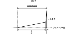
- FIG. 2A is a diagram illustrating a conduction band when no voltage is applied.
- FIG. 2B is a diagram illustrating a conduction band when a predetermined voltage is applied.
- FIG. 3 is a diagram illustrating the relationship between the interelectrode voltage and the capacitance.
- FIG. 4 is a diagram illustrating an example of the configuration of the switching circuit.
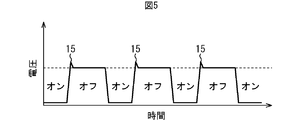
- FIG. 5 is a diagram illustrating an example of the operation of the switching circuit.
- FIG. 6 is a cross-sectional view showing a modification of the first embodiment.
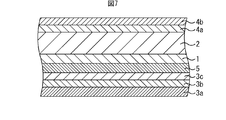
- FIG. 7 is a cross-sectional view showing another modification of the first embodiment.
- FIG. 8A is a cross-sectional view illustrating a method for manufacturing a surge countermeasure element.
- FIG. 8B is a cross-sectional view illustrating a method for manufacturing the surge countermeasure element, following FIG. 8A.
- FIG. 9 is a diagram showing the configuration of the MOCVD apparatus.
- FIG. 10 is a cross-sectional view showing the structure of the compound semiconductor device according to the second embodiment.
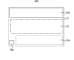
- FIG. 11 is a plan view showing the structure of the compound semiconductor device according to the second embodiment.
- FIG. 12A is a cross-sectional view illustrating the method of manufacturing the compound semiconductor device according to the second embodiment.
- FIG. 12B is a cross-sectional view illustrating a method for manufacturing the compound semiconductor device, following FIG. 12A.
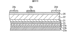
- FIG. 12C is a cross-sectional view showing a method for manufacturing the compound semiconductor device, following FIG. 12B.
- FIG. 1 is a cross-sectional view showing the structure of the compound semiconductor device (surge countermeasure element) according to the first embodiment.
- an intrinsic compound semiconductor layer 1 is formed above the electrode 3, and the band gap is larger than the compound semiconductor layer 1 on the compound semiconductor layer 1. Is formed, and the electrode 4 is formed above the compound semiconductor layer 2.
- the compound semiconductor layer 1 includes AlN or AlGaN
- the compound semiconductor layer 2 includes GaN.
- the compound semiconductor layer 1 is thinner than the compound semiconductor layer 2, the thickness of the compound semiconductor layer 1 is about 1 nm to 1000 nm, and the thickness of the compound semiconductor layer 2 is about 10 nm to 10000 nm.
- the conduction bands of the compound semiconductor layer 1 and the compound semiconductor layer 2 are higher than the Fermi level as shown in FIG. 2A.
- the compound semiconductor layer 1 and the compound semiconductor layer 2 function as a capacitive insulating film.
- the conduction band of the compound semiconductor layer 2 is lowered.
- the conduction band at the boundary between the compound semiconductor layer 1 and the compound semiconductor layer 2 decreases to the Fermi level, and the compound semiconductor layer Only 2 functions as a capacitive insulating film. That is, when the potential difference between the electrode 3 and the electrode 4 reaches a certain value, the effective distance of the capacitance between the electrode 3 and the electrode 4 is rapidly reduced, and the surge resistance is increased.
- the capacitance between the electrode 3 and the electrode 4 is extremely small.
- the potential difference between the electrode 3 and the electrode 4 is equal to or greater than the threshold value, the capacitance between the electrode 3 and the electrode 4 increases rapidly, and the surge resistance increases.
- the surge countermeasure element 10 can be used by connecting to a HEMT 11 used as a switching element of a switching circuit, for example, as shown in FIG. That is, the electrode 3 of the surge countermeasure element 10 may be connected to the drain of the HEMT 11 connected between the terminal supplied with the power supply voltage and the ground terminal, and the electrode 4 may be connected to the source.
- the HEMT 11 that is a switching element is repeatedly turned on and off as shown in FIG. At the time of switching from on to off, a surge occurs due to the influence of the inductor 12 parasitic on the switching circuit, but the capacity of the surge countermeasure element 10 increases quickly without being inferior to the operating speed of the HEMT 11. Therefore, the rounding of the signal waveform accompanying the occurrence of surge can be suppressed.
- the HEMT 11 can be operated with high efficiency. It is also possible to maintain the high-speed operation of the HEMT 11. Furthermore, when an excessive surge flows in, the HEMT 11 can be appropriately protected.
- the compound semiconductor layer 2 is doped p-type. This is because a higher breakdown voltage can be obtained when a p-type impurity is doped.
- a compound semiconductor layer 5 having a band gap smaller than that of the compound semiconductor layer 1 may be formed between the electrode 3 and the compound semiconductor layer 1.
- the compound semiconductor layer 5 includes n-type or intrinsic GaN.
- the thickness of the compound semiconductor layer 5 is about 1 nm to 5000 nm. Depending on the thickness of the compound semiconductor layer 5 and the impurity concentration distribution, the interelectrode voltage at which the capacitance of the surge countermeasure element changes rapidly, the operating speed, and the like can be adjusted.
- a stacked body including a conductive substrate 3 a, a conductive buffer layer 3 b, and a contact layer 3 c may be used as the electrode 3, and the contact layer 4 a and the metal film 4 b are used as the electrode 4.
- the conductive substrate 3a is, for example, a conductive Si substrate, a conductive SiC substrate, a conductive GaN substrate, or the like.
- the conductive substrate 3a is doped with, for example, n-type impurities.
- the conductive buffer layer 3b includes n-type AlN or AlGaN
- the contact layer 3c includes n-type GaN.
- the conductive buffer layer 3b is about 1 nm to 1000 nm, and the thickness of the contact layer 3c is about 1 nm to 5000 nm.
- the contact layer 4a includes n-type GaN and has a thickness of about 1 nm to 5000 nm.
- the metal film 4b includes, for example, a stacked body of a Ta film having a thickness of about 20 nm and an Al film having a thickness of about 200 nm thereon.
- the compound semiconductor layer 5 is provided as in the example shown in FIG. 6, but the compound semiconductor layer 5 may not be provided as in the example shown in FIG.
- FIG. 7 is a method for manufacturing the surge countermeasure element shown in FIG. 7 .
- 8A to 8B are cross-sectional views showing a method of manufacturing a surge countermeasure element in the order of steps.
- a conductive buffer layer 3b, a contact layer 3c, a compound semiconductor layer 5, a compound semiconductor layer 1, a compound semiconductor layer 2, and a contact layer 4a are formed on, for example, organic chemistry on a conductive substrate 3a. It is formed by vapor deposition (MOCVD: metal-organic-chemical-vapor-deposition) method. These may be formed by a molecular beam epitaxy (MBE) method.
- MOCVD metal-organic-chemical-vapor-deposition
- FIG. 9 is a diagram showing the configuration of the MOCVD apparatus.
- a high frequency coil 141 is disposed around the quartz reaction tube 140, and a carbon susceptor 142 for placing the substrate 120 is disposed inside the reaction tube 140.
- Two gas introduction pipes 144 and 145 are connected to the upstream end of the reaction tube 140 (the left end in FIG. 9), and a compound source gas is supplied.
- NH 3 gas is introduced from the gas introduction pipe 144 as an N source gas
- organic group III compound materials such as trimethylaluminum (TMA) and trimethylgallium (TMG) are introduced from the gas introduction pipe 145 as a group III element source gas. Is done.
- Crystal growth is performed on the substrate 120, and excess gas is discharged from the gas discharge pipe 146 to the detoxification tower.
- the gas exhaust pipe 146 is connected to a vacuum pump, and the exhaust port of the vacuum pump is connected to a detoxification tower.
- the presence / absence and flow rate of the TMA gas as the Al source and the TMG gas as the Ga source are appropriately set according to the type of layer to be formed.
- an n-type impurity for example, a gas containing Si, for example, SiH 4 gas is added to the raw material gas at a predetermined flow rate, and Si is doped so as to be a predetermined value within each of the above concentration ranges. .
- TMA Trimethylaluminum
- NH 3 Ammonia
- Pressure 100 Torr
- Temperature 1100 ° C.
- the conditions for forming the GaN layer are set as follows, for example. Trimethylgallium (TMG) flow rate: 1-50 sccm, Ammonia (NH 3 ) flow rate: 10-10000 sccm, Pressure: 100 Torr, Temperature: 1100 ° C.
- the conditions for forming the Al 0.25 Ga 0.75 N layer as the AlGaN layer are set as follows, for example. Trimethylgallium (TMG) flow rate: 0-50 sccm, Trimethylaluminum (TMA) flow rate: 0-50 sccm, Ammonia (NH 3 ) flow rate: 20 slm, Pressure: 100 Torr, Temperature: 1100 ° C.
- the conditions for forming the n-type GaN layer are set as follows, for example. Trimethylgallium (TMG) flow rate: 1-50 sccm, Ammonia (NH 3 ) flow rate: 10-10000 sccm, n-type impurity: silane (SiH 4 ), Pressure: 100 Torr, Temperature: 1100 ° C.
- TMG Trimethylgallium
- NH 3 Ammonia
- n-type impurity silane
- Pressure 100 Torr
- Temperature 1100 ° C.
- a metal film 4b is formed on the contact layer 4a.
- the metal film 4b can be formed by sputtering, for example.
- the surge countermeasure element shown in FIG. 7 can be manufactured.
- the surge countermeasure element shown in FIG. 1 and the surge countermeasure element shown in FIG. 6 can be manufactured by a similar process.
- FIG. 10 is a cross-sectional view showing the structure of the compound semiconductor device according to the second embodiment.
- This compound semiconductor device includes a GaN-based HEMT and a surge countermeasure element.
- the conductive buffer layer 23b on the conductive substrate 23a, the conductive buffer layer 23b, the contact layer 23c, the GaN layer 25, the intrinsic AlN layer 21, the GaN layer 22,
- an n-type AlGaN layer 26 is formed on the AlGaN layer 26.
- a gate electrode 24g is formed on the AlGaN layer 26.
- a source electrode 24s and a drain electrode 24d are also formed so as to sandwich the gate electrode 24g in plan view.
- the conductive substrate 23a is, for example, a conductive Si substrate, a conductive SiC substrate, a conductive GaN substrate, or the like.
- the conductive substrate 23a is doped with, for example, n-type impurities.
- the conductive buffer layer 23b contains n-type AlN or AlGaN and has a thickness of about 1 nm to 1000 nm.
- the contact layer 23c includes n-type GaN and has a thickness of about 1 nm to 5000 nm.
- the thickness of the GaN layer 25 is about 1 nm to 5000 nm
- the thickness of the AlN layer 21 is about nm to 1000 nm
- the thickness of the GaN layer 22 is about 10 nm to 10000 nm
- the thickness of the AlGaN layer 26 Is about 1 nm to 200 nm.
- the gate electrode 24g includes, for example, a stacked body of a Ni film having a thickness of about 30 nm and an Au film having a thickness of about 400 nm thereon.
- the source electrode 24s and the drain electrode 24d include, for example, a stacked body of a Ta film having a thickness of about 20 nm and an Al film having a thickness of about 200 nm thereon.
- the drain electrode 24d is connected to the conductive substrate 23a.
- the GaN layer 22 functions as an electron transit layer of the HEMT, and the AlGaN layer 26 functions as an electron supply layer.
- the AlN layer 21 functions in the same manner as the compound semiconductor layer 1 of the surge countermeasure element 10 according to the first embodiment, and the GaN layer 22 functions as the compound semiconductor layer 2 of the surge countermeasure element 10 according to the first embodiment. Works the same way.
- the HEMT included in the compound semiconductor device according to the second embodiment can perform an appropriate operation at high speed by the action of the surge countermeasure element.
- such a laminated structure is covered with a passivation film 27 such as a silicon nitride film.
- the gate electrode 24g is connected to the gate pad 28g
- the source electrode 24s is connected to the source pad 28s
- the drain electrode 24d is connected to the drain pad 28d.
- the gate pad 28g, the source pad 28s, and the drain pad 28d are exposed from the passivation film 27, and bonding wires or terminals are connected to these.
- the HEMT shown in FIG. 10 is arranged in the transistor region 29.
- An AlGaN layer may be formed instead of the AlN layer 21. Further, an intrinsic AlGaN layer may be formed as a spacer layer between the GaN layer 22 and the AlGaN layer 26.
- At least a part of the GaN layer 22 is doped p-type. This is because a higher breakdown voltage can be obtained when a p-type impurity is doped.
- 12A to 12C are cross-sectional views showing a method of manufacturing a surge countermeasure element in the order of steps.
- a conductive buffer layer 23b, a contact layer 23c, a GaN layer 25, an intrinsic AlN layer 21, a GaN layer 22, and an n-type AlGaN layer 26 are formed on a conductive substrate 23a. It is formed by the MOCVD method. These may be formed by the MBE method.
- the source electrode 24s and the drain electrode 24d are formed on the AlGaN layer 26 as shown in FIG. 12B.
- the source electrode 24s and the drain electrode 24d can be formed by, for example, a lift-off method. That is, a resist pattern in which an opening for opening a region where the source electrode 24s is to be formed and an opening for opening a region where the drain electrode 24d is to be formed is formed, and a Ta film and an Al film are formed by sputtering, for example. And the resist pattern may be removed together with the Ta film and Al film thereon.
- the gate electrode 24g is formed on the AlGaN layer 26 so as to be sandwiched between the source electrode 24s and the drain electrode 24d in plan view.
- the gate electrode 24g is formed near the source electrode 24s, for example.
- the gate electrode 24g can be formed by, for example, a lift-off method. That is, a resist pattern in which an opening for opening a region where the gate electrode 24g is to be formed is formed, a Ni film and an Au film are formed by, for example, vapor deposition, and the resist pattern is formed on the Ni film and the Au film thereon. And should be removed together.
- the compound semiconductor device according to the second embodiment can be manufactured.
- a stacked body of the conductive substrate 23a, the conductive buffer layer 23b, and the contact layer 23c can be regarded as one electrode.
- the HEMT (compound semiconductor device) combined with the surge countermeasure element 10 according to the first embodiment and the compound semiconductor device according to the second embodiment can be used for a switching element, for example.
- a switching element can be used for a switching power supply or an electronic device.
- these compound semiconductor devices can be used as components for a full bridge power supply circuit such as a server power supply circuit.
Landscapes
- Junction Field-Effect Transistors (AREA)
Abstract
第1の電極(3)と、第1の電極(3)の上方に形成された真性の第1の化合物半導体層(1)と、第1の化合物半導体層(1)上に形成され、第1の化合物半導体層(1)よりもバンドギャップが小さい第2の化合物半導体層(2)と、第2の化合物半導体層(2)の上方に形成された第2の電極(4)と、が設けられている。
Description
本発明は、化合物半導体装置及びその製造方法に関する。
従来、基板の上方に結晶成長によりAlGaN層及びGaN層が形成され、GaN層が電子走行層として機能する高電子移動度トランジスタ(HEMT:high electron mobility transistor)についての研究が行われている。GaNのバンドギャップは3.4eVであり、Siのバンドギャップ(1.1eV)及びGaAsのバンドギャップ(1.4eV)よりも大きい。このため、GaN系のHEMTの耐圧は高く、自動車用等の高耐圧電力デバイスとして有望である。
その一方で、Si系の電界効果トランジスタには必然的にボディダイオードが存在する。ボディダイオードは逆並列となるようにトランジスタに接続されており、短時間のダイ電圧(サージ)が発生した場合でもアバランシェ崩壊を起こすことによって十分なサージ耐性を有している。しかし、GaN系のHEMTには、このようなボディダイオードが必然的には存在せず、サージが発生した場合に故障等が生じ得る。従来、サージ対策素子としては、バリスタ及びRCサージ吸収回路等が用いられている。
しかしながら、これらサージ対策素子には大きな容量が寄生しているため、発熱が大きくなったり、HEMTの動作が遅くなったりする。大きな発熱は動作効率の低下に繋がり、HEMTの動作速度の遅延はスイッチング素子におけるスイッチングロスに繋がる。また、HEMTの通常の動作時にこれらの素子に貫通電流が流れやすいため、消費電力が大きくなってしまう。更に、HEMTの動作速度がこれらサージ対策素子よりも速いため、サージ対策素子を用いても、サージ対策素子が動作する前にHEMTに電流が流れることがある。
本発明は、寄生容量の増加を抑えながらサージの影響を抑制することができる化合物半導体装置及びその製造方法を提供することを目的とする。
化合物半導体装置の一態様には、第1の電極と、前記第1の電極の上方に形成された真性の第1の化合物半導体層と、前記第1の化合物半導体層上に形成され、前記第1の化合物半導体層よりもバンドギャップが小さい第2の化合物半導体層と、前記第2の化合物半導体層の上方に形成された第2の電極と、が設けられている。
化合物半導体装置の他の一態様には、導電性基板と、前記導電性基板の上方に形成された真性の第1の化合物半導体層と、前記第1の化合物半導体層上に形成され、前記第1の化合物半導体層よりもバンドギャップが小さい電子走行層としての第2の化合物半導体層と、前記第2の化合物半導体層の上方に形成された電子供給層と、前記電子供給層の上方に形成されたソース電極、ゲート電極及びドレイン電極と、が設けられている。前記導電性基板と前記ドレイン電極とが互いに接続されている。
化合物半導体装置の製造方法の一態様では、第1の電極の上方に真性の第1の化合物半導体層を形成し、前記第1の化合物半導体層上に、前記第1の化合物半導体層よりもバンドギャップが小さい第2の化合物半導体層を形成する。また、前記第2の化合物半導体層の上方に第2の電極を形成する。
上記の化合物半導体装置等によれば、真性の第1の化合物半導体層及び第2の化合物半導体層のバンドギャップの関係が適切なものとなっているため、寄生容量の増加を抑制しつつサージの影響を抑制することができる。
以下、実施形態について、添付の図面を参照して具体的に説明する。
(第1の実施形態)
先ず、第1の実施形態について説明する。図1は、第1の実施形態に係る化合物半導体装置(サージ対策素子)の構造を示す断面図である。
先ず、第1の実施形態について説明する。図1は、第1の実施形態に係る化合物半導体装置(サージ対策素子)の構造を示す断面図である。
第1の実施形態に係るサージ対策素子10では、図1に示すように、電極3の上方に真性の化合物半導体層1が形成され、化合物半導体層1上に、化合物半導体層1よりもバンドギャップが小さい化合物半導体層2が形成され、化合物半導体層2の上方に電極4が形成されている。例えば、化合物半導体層1はAlN又はAlGaNを含み、化合物半導体層2はGaNを含む。例えば、化合物半導体層1は化合物半導体層2よりも薄く、化合物半導体層1の厚さは1nm~1000nm程度であり、化合物半導体層2の厚さは10nm~10000nm程度である。
このサージ対策素子10では、電極3及び電極4の間に電圧が印加されていない場合には、図2Aに示すように、化合物半導体層1及び化合物半導体層2の伝導帯がフェルミレベルよりも高く、化合物半導体層1及び化合物半導体層2が容量絶縁膜として機能する。また、電極4よりも電極3に高い電位が印加されると、化合物半導体層2の伝導帯が下がる。そして、電極4よりも電極3にある値だけ高い電位が印加されると、図2Bに示すように、化合物半導体層1及び化合物半導体層2の境界の伝導帯がフェルミレベルまで下がり、化合物半導体層2のみが容量絶縁膜として機能する。つまり、電極3及び電極4の間の電位差がある値に達すると、電極3及び電極4の間の容量の実効距離が急激に減少し、サージ耐量が増大する。
例えば、図3に示すように、電極3及び電極4の間の電位差(電極間電圧)がある閾値(約550V)未満であれば、電極3及び電極4の間の容量は極めて小さい。一方、電極3及び電極4の間の電位差が閾値以上となると、電極3及び電極4の間の容量が急激に増加し、サージ耐量が増大する。
サージ対策素子10は、例えば、図4に示すように、スイッチング回路のスイッチング素子として用いられるHEMT11に接続して用いることができる。すなわち、電源電圧が供給される端子と接地端子との間に接続されたHEMT11のドレインにサージ対策素子10の電極3を接続し、ソースに電極4を接続すればよい。このように構成されたスイッチング回路では、図5に示すように、スイッチング素子であるHEMT11のオン及びオフが繰り返される。オンからオフへの切り替えの際に、スイッチング回路に寄生しているインダクタ12の影響でサージが発生するが、HEMT11の動作速度に劣ることなく、速やかにサージ対策素子10の容量が増加する。従って、サージの発生に伴う信号波形のなまりを抑制することができる。
このように、第1の実施形態によれば、HEMT11の通常動作時では、サージ対策素子10に電流が流れにくく、発熱及び消費電力の増大を抑制することができる。従って、HEMT11を高効率で動作させることができる。また、HEMT11の高速動作を維持することも可能である。更に、過大なサージが流入した場合には、HEMT11を適切に保護することができる。
なお、化合物半導体層2の少なくとも一部がp型にドープされていることが好ましい。p型の不純物がドープされていると、より高い耐圧を得ることができるためである。
なお、図6に示すように、電極3と化合物半導体層1との間に、化合物半導体層1よりもバンドギャップが小さい化合物半導体層5が形成されていてもよい。例えば、化合物半導体層5はn型又は真性のGaNを含む。また、例えば、化合物半導体層5の厚さは1nm~5000nm程度である。化合物半導体層5の厚さと不純物濃度分布に応じて、サージ対策素子の容量が急激に変化する電極間電圧、動作速度等を調整することができる。
また、図7に示すように、電極3として、導電性基板3a、導電性バッファ層3b、及びコンタクト層3cを含む積層体が用いられてもよく、電極4として、コンタクト層4a及び金属膜4bの積層体が用いられてもよい。導電性基板3aは、例えば導電性Si基板、導電性SiC基板、導電性GaN基板等である。導電性基板3aには、例えばn型の不純物がドープされている。例えば、導電性バッファ層3bはn型のAlN又はAlGaNを含み、コンタクト層3cはn型のGaNを含む。また、例えば、導電性バッファ層3bは1nm~1000nm程度であり、コンタクト層3cの厚さは1nm~5000nm程度である。例えば、コンタクト層4aはn型のGaNを含み、その厚さは1nm~5000nm程度である。また、金属膜4bは、例えば、厚さが20nm程度のTa膜、及びその上の厚さが200nm程度のAl膜の積層体を含む。なお、図7に示す例では、図6に示す例のように化合物半導体層5が設けられているが、図1に示す例のように化合物半導体層5が設けられていなくてもよい。
次に、図7に示すサージ対策素子を製造する方法について説明する。図8A~図8Bは、サージ対策素子を製造する方法を工程順に示す断面図である。
先ず、図8Aに示すように、導電性基板3a上に、導電性バッファ層3b、コンタクト層3c、化合物半導体層5、化合物半導体層1、化合物半導体層2、及びコンタクト層4aを、例えば有機化学気相堆積(MOCVD:metal organic chemical vapor deposition)法により形成する。これらを分子線エピタキシー(MBE:molecular beam epitaxy)法により形成してもよい。
ここで、MOCVD装置について説明する。図9は、MOCVD装置の構成を示す図である。石英製反応管140の周囲に高周波コイル141が配置され、反応管140の内側に基板120を載置するためのカーボンサセプタ142が配置されている。反応管140の上流端(図9中の左側の端部)に、2本のガス導入管144及び145が接続され、化合物のソースガスが供給される。例えば、ガス導入管144からNソースガスとしてNH3ガスが導入され、ガス導入管145からIII族元素のソースガスとしてトリメチルアルミニウム(TMA)、トリメチルガリウム(TMG)等の有機III族化合物原料が導入される。基板120上で結晶成長が行われ、余剰のガスはガス排出管146から除害塔へ排出される。なお、MOCVD法による結晶成長を減圧雰囲気で行う場合は、ガス排出管146は真空ポンプへ接続され、真空ポンプの排出口が除害塔に接続される。
これらの形成の際には、形成しようとする層の種類に応じて、Al源であるTMAガス及びGa源であるTMGガスの供給の有無及び流量を適宜設定する。更に、n型不純物を含有させる場合には、例えばSiを含むガス、例えばSiH4ガスを所定の流量で原料ガスに添加し、上記の各濃度範囲内の所定値となるようにSiをドーピングする。
AlN層を形成する場合の条件は、例えば、以下のように設定する。
トリメチルアルミニウム(TMA)の流量:1~50sccm、
アンモニア(NH3)の流量:10~5000sccm、
圧力:100Torr、
温度:1100℃。
トリメチルアルミニウム(TMA)の流量:1~50sccm、
アンモニア(NH3)の流量:10~5000sccm、
圧力:100Torr、
温度:1100℃。
GaN層を形成する場合の条件は、例えば、以下のように設定する。
トリメチルガリウム(TMG)の流量:1~50sccm、
アンモニア(NH3)の流量:10~10000sccm、
圧力:100Torr、
温度:1100℃。
AlGaN層としてAl0.25Ga0.75N層を形成する場合の条件は、例えば、以下のように設定する。
トリメチルガリウム(TMG)の流量:0~50sccm、
トリメチルアルミニウム(TMA)の流量:0~50sccm、
アンモニア(NH3)の流量:20slm、
圧力:100Torr、
温度:1100℃。
トリメチルガリウム(TMG)の流量:1~50sccm、
アンモニア(NH3)の流量:10~10000sccm、
圧力:100Torr、
温度:1100℃。
AlGaN層としてAl0.25Ga0.75N層を形成する場合の条件は、例えば、以下のように設定する。
トリメチルガリウム(TMG)の流量:0~50sccm、
トリメチルアルミニウム(TMA)の流量:0~50sccm、
アンモニア(NH3)の流量:20slm、
圧力:100Torr、
温度:1100℃。
n型のGaN層を形成する場合の条件は、例えば、以下のように設定する。
トリメチルガリウム(TMG)の流量:1~50sccm、
アンモニア(NH3)の流量:10~10000sccm、
n型不純物:シラン(SiH4)、
圧力:100Torr、
温度:1100℃。
トリメチルガリウム(TMG)の流量:1~50sccm、
アンモニア(NH3)の流量:10~10000sccm、
n型不純物:シラン(SiH4)、
圧力:100Torr、
温度:1100℃。
コンタクト層4aを形成した後には、コンタクト層4a上に金属膜4bを形成する。金属膜4bは、例えばスパッタ法により形成することができる。
このようにして図7に示すサージ対策素子を製造することができる。図1に示すサージ対策素子、及び図6に示すサージ対策素子も、同様の処理により製造することができる。
(第2の実施形態)
次に、第2の実施形態について説明する。図10は、第2の実施形態に係る化合物半導体装置の構造を示す断面図である。この化合物半導体装置には、GaN系HEMT及びサージ対策素子が含まれている。
次に、第2の実施形態について説明する。図10は、第2の実施形態に係る化合物半導体装置の構造を示す断面図である。この化合物半導体装置には、GaN系HEMT及びサージ対策素子が含まれている。
第2の実施形態に係る化合物半導体装置では、図10に示すように、導電性基板23a上に、導電性バッファ層23b、コンタクト層23c、GaN層25、真性のAlN層21、GaN層22、及びn型のAlGaN層26が形成されている。また、AlGaN層26上にゲート電極24gが形成されている。AlGaN層26上には、平面視でゲート電極24gを間に挟むようにしてソース電極24s及びドレイン電極24dも形成されている。
導電性基板23aは、例えば導電性Si基板、導電性SiC基板、導電性GaN基板等である。導電性基板23aには、例えばn型の不純物がドープされている。例えば、導電性バッファ層23bはn型のAlN又はAlGaNを含み、その厚さは1nm~1000nm程度である。例えば、コンタクト層23cはn型のGaNを含み、その厚さは1nm~5000nm程度である。例えば、GaN層25の厚さは1nm~5000nm程度であり、AlN層21の厚さはnm~1000nm程度であり、GaN層22の厚さは10nm~10000nm程度であり、AlGaN層26の厚さは1nm~200nm程度である。ゲート電極24gは、例えば、厚さが30nm程度のNi膜、及びその上の厚さが400nm程度のAu膜の積層体を含む。ソース電極24s及びドレイン電極24dは、例えば、厚さが20nm程度のTa膜、及びその上の厚さが200nm程度のAl膜の積層体を含む。また、ドレイン電極24dは導電性基板23aに接続される。
このように構成された化合物半導体装置では、GaN層22がHEMTの電子走行層として機能し、AlGaN層26が電子供給層として機能する。また、AlN層21が、第1の実施形態に係るサージ対策素子10の化合物半導体層1と同様に機能し、GaN層22が、第1の実施形態に係るサージ対策素子10の化合物半導体層2と同様に機能する。
従って、第2の実施形態に係る化合物半導体装置に含まれるHEMTは、サージ対策素子の作用により、高速で適切な動作を行うことができる。
図11に示すように、このような積層構造は、シリコン窒化膜等のパッシベーション膜27により覆われている。ゲート電極24gはゲートパッド28gに接続され、ソース電極24sはソースパッド28sに接続され、ドレイン電極24dはドレインパッド28dに接続されている。ゲートパッド28g、ソースパッド28s、及びドレインパッド28dはパッシベーション膜27から露出しており、これらにボンディングワイヤ又は端子等が接続される。また、トランジスタ領域29には、図10に示すHEMTが配置されている。
なお、AlN層21の代わりにAlGaN層が形成されていてもよい。また、GaN層22とAlGaN層26との間に、スペーサ層として真性のAlGaN層が形成されていてもよい。
また、GaN層22の少なくとも一部がp型にドープされていることが好ましい。p型の不純物がドープされていると、より高い耐圧を得ることができるためである。
次に、第2の実施形態に係る化合物半導体装置を製造する方法について説明する。図12A~図12Cは、サージ対策素子を製造する方法を工程順に示す断面図である。
先ず、図12Aに示すように、導電性基板23a上に、導電性バッファ層23b、コンタクト層23c、GaN層25、真性のAlN層21、GaN層22、及びn型のAlGaN層26を、例えばMOCVD法により形成する。これらをMBE法により形成してもよい。
AlGaN層26を形成した後には、図12Bに示すように、AlGaN層26上にソース電極24s及びドレイン電極24dを形成する。ソース電極24s及びドレイン電極24dは、例えばリフトオフ法により形成することができる。つまり、ソース電極24sを形成する予定の領域を開口する開口部及びドレイン電極24dを形成する予定の領域を開口する開口部が形成されたレジストパターンを形成し、Ta膜及びAl膜を例えばスパッタ法により形成し、レジストパターンをその上のTa膜及びAl膜と共に除去すればよい。
ソース電極24s及びドレイン電極24dを形成した後には、図12Cに示すように、AlGaN層26上に、平面視でソース電極24s及びドレイン電極24dに挟まれるようにしてゲート電極24gを形成する。ゲート電極24gは、例えばソース電極24s寄りに形成する。ゲート電極24gは、例えばリフトオフ法により形成することができる。つまり、ゲート電極24gを形成する予定の領域を開口する開口部が形成されたレジストパターンを形成し、Ni膜及びAu膜を例えば蒸着法により形成し、レジストパターンをその上のNi膜及びAu膜と共に除去すればよい。
このようにして第2の実施形態に係る化合物半導体装置を製造することができる。なお、導電性基板23a、導電性バッファ層23b、及びコンタクト層23cの積層体を一つの電極とみなすことも可能である。
第1の実施形態に係るサージ対策素子10と組み合わせたHEMT(化合物半導体装置)、及び第2の実施形態に係る化合物半導体装置は、例えば、スイッチング素子に用いることができる。また、このようなスイッチング素子は、スイッチング電源又は電子機器に用いることができる。更に、これらの化合物半導体装置を、サーバの電源回路等のフルブリッジ電源回路用の部品として用いることも可能である。
これらの化合物半導体装置等によれば、寄生容量を低減しながらサージの影響を抑制することができる。
Claims (19)
- 第1の電極と、
前記第1の電極の上方に形成された真性の第1の化合物半導体層と、
前記第1の化合物半導体層上に形成され、前記第1の化合物半導体層よりもバンドギャップが小さい第2の化合物半導体層と、
前記第2の化合物半導体層の上方に形成された第2の電極と、
を有することを特徴とする化合物半導体装置。 - 前記第1の化合物半導体層及び前記第2の化合物半導体層は、窒化物半導体を含有することを特徴とする請求項1に記載の化合物半導体装置。
- 前記第1の化合物半導体層の窒化物半導体は、AlNであることを特徴とする請求項2に記載の化合物半導体装置。
- 前記第1の化合物半導体層の窒化物半導体は、AlGaNであることを特徴とする請求項2に記載の化合物半導体装置。
- 前記第1の電極と前記第1の化合物半導体層との間に、前記第1の化合物半導体層よりもバンドギャップが小さい第3の化合物半導体層を有することを特徴とする請求項1に記載の化合物半導体装置。
- 前記第3の化合物半導体層が窒化物半導体を含有することを特徴とする請求項5に記載の化合物半導体装置。
- 前記第2の化合物半導体層の少なくとも一部がp型にドープされていることを特徴とする請求項1に記載の化合物半導体装置。
- 導電性基板と、
前記導電性基板の上方に形成された真性の第1の化合物半導体層と、
前記第1の化合物半導体層上に形成され、前記第1の化合物半導体層よりもバンドギャップが小さい電子走行層としての第2の化合物半導体層と、
前記第2の化合物半導体層の上方に形成された電子供給層と、
前記電子供給層の上方に形成されたソース電極、ゲート電極及びドレイン電極と、
を有し、
前記導電性基板と前記ドレイン電極とが互いに接続されていることを特徴とする化合物半導体装置。 - 前記第1の化合物半導体層及び前記第2の化合物半導体層は、窒化物半導体を含有することを特徴とする請求項8に記載の化合物半導体装置。
- 前記第1の化合物半導体層の窒化物半導体は、AlNであることを特徴とする請求項9に記載の化合物半導体装置。
- 前記第1の化合物半導体層の窒化物半導体は、AlGaNであることを特徴とする請求項9に記載の化合物半導体装置。
- 前記導電性基板と前記第1の化合物半導体層との間に、前記第1の化合物半導体層よりもバンドギャップが小さい第3の化合物半導体層を有することを特徴とする請求項8に記載の化合物半導体装置。
- 前記第3の化合物半導体層が窒化物半導体を含有することを特徴とする請求項12に記載の化合物半導体装置。
- 前記第2の化合物半導体層の少なくとも一部がp型にドープされていることを特徴とする請求項8に記載の化合物半導体装置。
- 第1の電極の上方に真性の第1の化合物半導体層を形成する工程と、
前記第1の化合物半導体層上に、前記第1の化合物半導体層よりもバンドギャップが小さい第2の化合物半導体層を形成する工程と、
前記第2の化合物半導体層の上方に第2の電極を形成する工程と、
を有することを特徴とする化合物半導体装置の製造方法。 - 前記第2の化合物半導体層は、電子走行層であり、
前記第2の電極は、ソース電極、ゲート電極、及びドレイン電極であり、
前記第2の化合物半導体層を形成する工程と前記第2の電極を形成する工程との間に、前記第2の化合物半導体層の上方に電子供給層を形成する工程を有することを特徴とする請求項15に記載の化合物半導体装置の製造方法。 - 前記第1の化合物半導体層及び前記第2の化合物半導体層は、窒化物半導体を含有することを特徴とする請求項15に記載の化合物半導体装置の製造方法。
- 前記第1の化合物半導体層を形成する工程の前に、
前記第1の電極の上方に、前記第1の化合物半導体層よりもバンドギャップが小さい第3の化合物半導体層を形成する工程を有することを特徴とする請求項15に記載の化合物半導体装置の製造方法。 - 前記第3の化合物半導体層が窒化物半導体を含有することを特徴とする請求項18に記載の化合物半導体装置の製造方法。
Priority Applications (4)
| Application Number | Priority Date | Filing Date | Title |
|---|---|---|---|
| JP2013505630A JP5692357B2 (ja) | 2011-03-18 | 2011-03-18 | 化合物半導体装置及びその製造方法 |
| PCT/JP2011/056580 WO2012127567A1 (ja) | 2011-03-18 | 2011-03-18 | 化合物半導体装置及びその製造方法 |
| CN201180069251.XA CN103430294B (zh) | 2011-03-18 | 2011-03-18 | 化合物半导体装置及其制造方法 |
| US13/971,921 US8941093B2 (en) | 2011-03-18 | 2013-08-21 | Compound semiconductor device and manufacturing method thereof |
Applications Claiming Priority (1)
| Application Number | Priority Date | Filing Date | Title |
|---|---|---|---|
| PCT/JP2011/056580 WO2012127567A1 (ja) | 2011-03-18 | 2011-03-18 | 化合物半導体装置及びその製造方法 |
Related Child Applications (1)
| Application Number | Title | Priority Date | Filing Date |
|---|---|---|---|
| US13/971,921 Continuation US8941093B2 (en) | 2011-03-18 | 2013-08-21 | Compound semiconductor device and manufacturing method thereof |
Publications (1)
| Publication Number | Publication Date |
|---|---|
| WO2012127567A1 true WO2012127567A1 (ja) | 2012-09-27 |
Family
ID=46878764
Family Applications (1)
| Application Number | Title | Priority Date | Filing Date |
|---|---|---|---|
| PCT/JP2011/056580 Ceased WO2012127567A1 (ja) | 2011-03-18 | 2011-03-18 | 化合物半導体装置及びその製造方法 |
Country Status (4)
| Country | Link |
|---|---|
| US (1) | US8941093B2 (ja) |
| JP (1) | JP5692357B2 (ja) |
| CN (1) | CN103430294B (ja) |
| WO (1) | WO2012127567A1 (ja) |
Families Citing this family (1)
| Publication number | Priority date | Publication date | Assignee | Title |
|---|---|---|---|---|
| CN114335165B (zh) * | 2021-12-28 | 2025-10-31 | 湖南三安半导体有限责任公司 | 一种横向场效应管及其制备方法 |
Citations (3)
| Publication number | Priority date | Publication date | Assignee | Title |
|---|---|---|---|---|
| JPH10223901A (ja) * | 1996-12-04 | 1998-08-21 | Sony Corp | 電界効果型トランジスタおよびその製造方法 |
| JP2009004743A (ja) * | 2007-05-18 | 2009-01-08 | Sanken Electric Co Ltd | 電界効果半導体装置 |
| JP2010040814A (ja) * | 2008-08-06 | 2010-02-18 | Sharp Corp | 半導体装置 |
Family Cites Families (21)
| Publication number | Priority date | Publication date | Assignee | Title |
|---|---|---|---|---|
| US5929467A (en) | 1996-12-04 | 1999-07-27 | Sony Corporation | Field effect transistor with nitride compound |
| JP2000332362A (ja) * | 1999-05-24 | 2000-11-30 | Sony Corp | 半導体装置および半導体発光素子 |
| US6566692B2 (en) * | 2000-08-11 | 2003-05-20 | Matsushita Electric Industrial Co., Ltd. | Electron device and junction transistor |
| JP3771135B2 (ja) | 2001-02-26 | 2006-04-26 | 株式会社ルネサステクノロジ | 半導体開閉器 |
| US6674101B2 (en) * | 2001-06-01 | 2004-01-06 | Furukawa Electric Co Ltd | GaN-based semiconductor device |
| US6881261B2 (en) * | 2001-11-13 | 2005-04-19 | Matsushita Electric Industrial Co., Ltd. | Method for fabricating semiconductor device |
| JP4209136B2 (ja) * | 2002-05-30 | 2009-01-14 | パナソニック株式会社 | 半導体装置及びその製造方法 |
| US7714359B2 (en) * | 2005-02-17 | 2010-05-11 | Panasonic Corporation | Field effect transistor having nitride semiconductor layer |
| JP2007273640A (ja) * | 2006-03-30 | 2007-10-18 | Sanken Electric Co Ltd | 半導体装置 |
| JP5319084B2 (ja) | 2007-06-19 | 2013-10-16 | ルネサスエレクトロニクス株式会社 | 半導体装置 |
| JP2009164158A (ja) | 2007-12-28 | 2009-07-23 | Panasonic Corp | 半導体装置及びその製造方法 |
| JP5564791B2 (ja) * | 2008-12-26 | 2014-08-06 | 富士通株式会社 | 化合物半導体装置及びその製造方法 |
| US8195653B2 (en) * | 2009-01-07 | 2012-06-05 | Microsoft Corporation | Relevance improvements for implicit local queries |
| JP5487631B2 (ja) * | 2009-02-04 | 2014-05-07 | 富士通株式会社 | 化合物半導体装置及びその製造方法 |
| JP4794656B2 (ja) * | 2009-06-11 | 2011-10-19 | シャープ株式会社 | 半導体装置 |
| JP5481103B2 (ja) * | 2009-06-11 | 2014-04-23 | 株式会社東芝 | 窒化物半導体素子 |
| JP2011040676A (ja) * | 2009-08-18 | 2011-02-24 | Sanken Electric Co Ltd | 半導体装置及びその製造方法 |
| JP2011049271A (ja) * | 2009-08-26 | 2011-03-10 | Sanken Electric Co Ltd | 半導体装置 |
| JP2011187580A (ja) * | 2010-03-05 | 2011-09-22 | Sony Corp | 自励発振型半導体レーザ素子及びその駆動方法 |
| JP5765147B2 (ja) * | 2011-09-01 | 2015-08-19 | 富士通株式会社 | 半導体装置 |
| WO2013095643A1 (en) * | 2011-12-23 | 2013-06-27 | Intel Corporation | Iii-n material structure for gate-recessed transistors |
-
2011
- 2011-03-18 WO PCT/JP2011/056580 patent/WO2012127567A1/ja not_active Ceased
- 2011-03-18 JP JP2013505630A patent/JP5692357B2/ja not_active Expired - Fee Related
- 2011-03-18 CN CN201180069251.XA patent/CN103430294B/zh not_active Expired - Fee Related
-
2013
- 2013-08-21 US US13/971,921 patent/US8941093B2/en not_active Expired - Fee Related
Patent Citations (3)
| Publication number | Priority date | Publication date | Assignee | Title |
|---|---|---|---|---|
| JPH10223901A (ja) * | 1996-12-04 | 1998-08-21 | Sony Corp | 電界効果型トランジスタおよびその製造方法 |
| JP2009004743A (ja) * | 2007-05-18 | 2009-01-08 | Sanken Electric Co Ltd | 電界効果半導体装置 |
| JP2010040814A (ja) * | 2008-08-06 | 2010-02-18 | Sharp Corp | 半導体装置 |
Non-Patent Citations (2)
| Title |
|---|
| M. FAGERLIND ET AL.: "Investigation of the interface between silicon nitride passivations and AlGaN/AlN/GaN heterostructures by C(V) characterization of metal-insulator-semiconductor-heterostructure capacitors", JOURNAL OF APPLIED PHYSICS, vol. 108, no. 1, 13 July 2010 (2010-07-13), pages 014508-1 - 014508-6, XP012141821 * |
| MARCIN MICZEK ET AL.: "Effects of interface states and temperature on the C-V behavior of metal/insulator/AlGaN/GaN heterostructure capacitors", JOURNAL OF APPLIED PHYSICS, vol. 103, no. 10, 28 May 2008 (2008-05-28), pages 104510-1 - 104510-11, XP012108813 * |
Also Published As
| Publication number | Publication date |
|---|---|
| CN103430294B (zh) | 2016-11-09 |
| CN103430294A (zh) | 2013-12-04 |
| US20130334540A1 (en) | 2013-12-19 |
| JP5692357B2 (ja) | 2015-04-01 |
| JPWO2012127567A1 (ja) | 2014-07-24 |
| US8941093B2 (en) | 2015-01-27 |
Similar Documents
| Publication | Publication Date | Title |
|---|---|---|
| JP5784440B2 (ja) | 半導体装置の製造方法及び半導体装置 | |
| JP5323527B2 (ja) | GaN系電界効果トランジスタの製造方法 | |
| US8963164B2 (en) | Compound semiconductor device and method of manufacturing the same | |
| JP5573941B2 (ja) | 化合物半導体装置及びその製造方法 | |
| JP5634681B2 (ja) | 半導体素子 | |
| JP4897948B2 (ja) | 半導体素子 | |
| JP5566670B2 (ja) | GaN系電界効果トランジスタ | |
| JP5712583B2 (ja) | 化合物半導体装置及びその製造方法 | |
| US8912572B2 (en) | High electron mobility transistor and method of manufacturing the same | |
| KR102944587B1 (ko) | 고전자이동도 트랜지스터 및 그 제조 방법 | |
| JP5546104B2 (ja) | GaN系電界効果トランジスタ | |
| JP7099255B2 (ja) | 化合物半導体装置、高周波増幅器及び電源装置 | |
| JP5170885B2 (ja) | 電界効果トランジスタ及びその製造方法 | |
| JP5510544B2 (ja) | 化合物半導体装置及びその製造方法 | |
| JP5707903B2 (ja) | 化合物半導体装置及びその製造方法 | |
| JP5935425B2 (ja) | 半導体装置 | |
| JP5692357B2 (ja) | 化合物半導体装置及びその製造方法 | |
| JP2022016952A (ja) | 半導体装置 | |
| JP6187167B2 (ja) | 化合物半導体装置及びその製造方法 | |
| TWI748225B (zh) | 增強型高電子遷移率電晶體元件 | |
| US10453948B2 (en) | Semiconductor device which comprises transistor and diode |
Legal Events
| Date | Code | Title | Description |
|---|---|---|---|
| 121 | Ep: the epo has been informed by wipo that ep was designated in this application |
Ref document number: 11861335 Country of ref document: EP Kind code of ref document: A1 |
|
| ENP | Entry into the national phase |
Ref document number: 2013505630 Country of ref document: JP Kind code of ref document: A |
|
| NENP | Non-entry into the national phase |
Ref country code: DE |
|
| 122 | Ep: pct application non-entry in european phase |
Ref document number: 11861335 Country of ref document: EP Kind code of ref document: A1 |