WO2012124522A1 - 発光装置、照明装置、前照灯および車両 - Google Patents
発光装置、照明装置、前照灯および車両 Download PDFInfo
- Publication number
- WO2012124522A1 WO2012124522A1 PCT/JP2012/055565 JP2012055565W WO2012124522A1 WO 2012124522 A1 WO2012124522 A1 WO 2012124522A1 JP 2012055565 W JP2012055565 W JP 2012055565W WO 2012124522 A1 WO2012124522 A1 WO 2012124522A1
- Authority
- WO
- WIPO (PCT)
- Prior art keywords
- light source
- laser
- laser light
- wiring
- emitting device
- Prior art date
- Legal status (The legal status is an assumption and is not a legal conclusion. Google has not performed a legal analysis and makes no representation as to the accuracy of the status listed.)
- Ceased
Links
Images






Classifications
-
- F—MECHANICAL ENGINEERING; LIGHTING; HEATING; WEAPONS; BLASTING
- F21—LIGHTING
- F21S—NON-PORTABLE LIGHTING DEVICES; SYSTEMS THEREOF; VEHICLE LIGHTING DEVICES SPECIALLY ADAPTED FOR VEHICLE EXTERIORS
- F21S41/00—Illuminating devices specially adapted for vehicle exteriors, e.g. headlamps
- F21S41/10—Illuminating devices specially adapted for vehicle exteriors, e.g. headlamps characterised by the light source
- F21S41/14—Illuminating devices specially adapted for vehicle exteriors, e.g. headlamps characterised by the light source characterised by the type of light source
-
- F—MECHANICAL ENGINEERING; LIGHTING; HEATING; WEAPONS; BLASTING
- F21—LIGHTING
- F21S—NON-PORTABLE LIGHTING DEVICES; SYSTEMS THEREOF; VEHICLE LIGHTING DEVICES SPECIALLY ADAPTED FOR VEHICLE EXTERIORS
- F21S41/00—Illuminating devices specially adapted for vehicle exteriors, e.g. headlamps
- F21S41/10—Illuminating devices specially adapted for vehicle exteriors, e.g. headlamps characterised by the light source
- F21S41/14—Illuminating devices specially adapted for vehicle exteriors, e.g. headlamps characterised by the light source characterised by the type of light source
- F21S41/16—Laser light sources
-
- F—MECHANICAL ENGINEERING; LIGHTING; HEATING; WEAPONS; BLASTING
- F21—LIGHTING
- F21S—NON-PORTABLE LIGHTING DEVICES; SYSTEMS THEREOF; VEHICLE LIGHTING DEVICES SPECIALLY ADAPTED FOR VEHICLE EXTERIORS
- F21S41/00—Illuminating devices specially adapted for vehicle exteriors, e.g. headlamps
- F21S41/10—Illuminating devices specially adapted for vehicle exteriors, e.g. headlamps characterised by the light source
- F21S41/14—Illuminating devices specially adapted for vehicle exteriors, e.g. headlamps characterised by the light source characterised by the type of light source
- F21S41/176—Light sources where the light is generated by photoluminescent material spaced from a primary light generating element
-
- F—MECHANICAL ENGINEERING; LIGHTING; HEATING; WEAPONS; BLASTING
- F21—LIGHTING
- F21S—NON-PORTABLE LIGHTING DEVICES; SYSTEMS THEREOF; VEHICLE LIGHTING DEVICES SPECIALLY ADAPTED FOR VEHICLE EXTERIORS
- F21S45/00—Arrangements within vehicle lighting devices specially adapted for vehicle exteriors, for purposes other than emission or distribution of light
- F21S45/70—Prevention of harmful light leakage
-
- F—MECHANICAL ENGINEERING; LIGHTING; HEATING; WEAPONS; BLASTING
- F21—LIGHTING
- F21V—FUNCTIONAL FEATURES OR DETAILS OF LIGHTING DEVICES OR SYSTEMS THEREOF; STRUCTURAL COMBINATIONS OF LIGHTING DEVICES WITH OTHER ARTICLES, NOT OTHERWISE PROVIDED FOR
- F21V9/00—Elements for modifying spectral properties, polarisation or intensity of the light emitted, e.g. filters
- F21V9/30—Elements containing photoluminescent material distinct from or spaced from the light source
-
- H—ELECTRICITY
- H01—ELECTRIC ELEMENTS
- H01S—DEVICES USING THE PROCESS OF LIGHT AMPLIFICATION BY STIMULATED EMISSION OF RADIATION [LASER] TO AMPLIFY OR GENERATE LIGHT; DEVICES USING STIMULATED EMISSION OF ELECTROMAGNETIC RADIATION IN WAVE RANGES OTHER THAN OPTICAL
- H01S5/00—Semiconductor lasers
-
- H—ELECTRICITY
- H01—ELECTRIC ELEMENTS
- H01S—DEVICES USING THE PROCESS OF LIGHT AMPLIFICATION BY STIMULATED EMISSION OF RADIATION [LASER] TO AMPLIFY OR GENERATE LIGHT; DEVICES USING STIMULATED EMISSION OF ELECTROMAGNETIC RADIATION IN WAVE RANGES OTHER THAN OPTICAL
- H01S5/00—Semiconductor lasers
- H01S5/005—Optical components external to the laser cavity, specially adapted therefor, e.g. for homogenisation or merging of the beams or for manipulating laser pulses, e.g. pulse shaping
- H01S5/0087—Optical components external to the laser cavity, specially adapted therefor, e.g. for homogenisation or merging of the beams or for manipulating laser pulses, e.g. pulse shaping for illuminating phosphorescent or fluorescent materials, e.g. using optical arrangements specifically adapted for guiding or shaping laser beams illuminating these materials
-
- F—MECHANICAL ENGINEERING; LIGHTING; HEATING; WEAPONS; BLASTING
- F21—LIGHTING
- F21Y—INDEXING SCHEME ASSOCIATED WITH SUBCLASSES F21K, F21L, F21S and F21V, RELATING TO THE FORM OR THE KIND OF THE LIGHT SOURCES OR OF THE COLOUR OF THE LIGHT EMITTED
- F21Y2101/00—Point-like light sources
-
- F—MECHANICAL ENGINEERING; LIGHTING; HEATING; WEAPONS; BLASTING
- F21—LIGHTING
- F21Y—INDEXING SCHEME ASSOCIATED WITH SUBCLASSES F21K, F21L, F21S and F21V, RELATING TO THE FORM OR THE KIND OF THE LIGHT SOURCES OR OF THE COLOUR OF THE LIGHT EMITTED
- F21Y2115/00—Light-generating elements of semiconductor light sources
- F21Y2115/30—Semiconductor lasers
-
- H—ELECTRICITY
- H01—ELECTRIC ELEMENTS
- H01S—DEVICES USING THE PROCESS OF LIGHT AMPLIFICATION BY STIMULATED EMISSION OF RADIATION [LASER] TO AMPLIFY OR GENERATE LIGHT; DEVICES USING STIMULATED EMISSION OF ELECTROMAGNETIC RADIATION IN WAVE RANGES OTHER THAN OPTICAL
- H01S5/00—Semiconductor lasers
- H01S5/005—Optical components external to the laser cavity, specially adapted therefor, e.g. for homogenisation or merging of the beams or for manipulating laser pulses, e.g. pulse shaping
-
- H—ELECTRICITY
- H01—ELECTRIC ELEMENTS
- H01S—DEVICES USING THE PROCESS OF LIGHT AMPLIFICATION BY STIMULATED EMISSION OF RADIATION [LASER] TO AMPLIFY OR GENERATE LIGHT; DEVICES USING STIMULATED EMISSION OF ELECTROMAGNETIC RADIATION IN WAVE RANGES OTHER THAN OPTICAL
- H01S5/00—Semiconductor lasers
- H01S5/005—Optical components external to the laser cavity, specially adapted therefor, e.g. for homogenisation or merging of the beams or for manipulating laser pulses, e.g. pulse shaping
- H01S5/0078—Optical components external to the laser cavity, specially adapted therefor, e.g. for homogenisation or merging of the beams or for manipulating laser pulses, e.g. pulse shaping for frequency filtering
-
- H—ELECTRICITY
- H01—ELECTRIC ELEMENTS
- H01S—DEVICES USING THE PROCESS OF LIGHT AMPLIFICATION BY STIMULATED EMISSION OF RADIATION [LASER] TO AMPLIFY OR GENERATE LIGHT; DEVICES USING STIMULATED EMISSION OF ELECTROMAGNETIC RADIATION IN WAVE RANGES OTHER THAN OPTICAL
- H01S5/00—Semiconductor lasers
- H01S5/04—Processes or apparatus for excitation, e.g. pumping, e.g. by electron beams
- H01S5/042—Electrical excitation ; Circuits therefor
-
- H—ELECTRICITY
- H01—ELECTRIC ELEMENTS
- H01S—DEVICES USING THE PROCESS OF LIGHT AMPLIFICATION BY STIMULATED EMISSION OF RADIATION [LASER] TO AMPLIFY OR GENERATE LIGHT; DEVICES USING STIMULATED EMISSION OF ELECTROMAGNETIC RADIATION IN WAVE RANGES OTHER THAN OPTICAL
- H01S5/00—Semiconductor lasers
- H01S5/06—Arrangements for controlling the laser output parameters, e.g. by operating on the active medium
- H01S5/068—Stabilisation of laser output parameters
- H01S5/06825—Protecting the laser, e.g. during switch-on/off, detection of malfunctioning or degradation
-
- H—ELECTRICITY
- H01—ELECTRIC ELEMENTS
- H01S—DEVICES USING THE PROCESS OF LIGHT AMPLIFICATION BY STIMULATED EMISSION OF RADIATION [LASER] TO AMPLIFY OR GENERATE LIGHT; DEVICES USING STIMULATED EMISSION OF ELECTROMAGNETIC RADIATION IN WAVE RANGES OTHER THAN OPTICAL
- H01S5/00—Semiconductor lasers
- H01S5/40—Arrangement of two or more semiconductor lasers, not provided for in groups H01S5/02 - H01S5/30
- H01S5/4018—Lasers electrically in series
Definitions
- the present invention relates to a light emitting device using a semiconductor laser element (LD; Laser Diode) as a light source, a lighting device and a headlamp provided with the light emitting device, and a vehicle equipped with the headlight.
- LD semiconductor laser element
- a detection resistor for detecting a break or a short circuit of the power supply line is inserted into the power supply line, and the comparison result between the detection potential of the detection resistor and the reference potential Therefore, the power supply to the LD is cut off.
- the amount of strain generated in the light guide path through which the laser light passes is detected, and the detection of the detection results in blocking the energization of the LD.
- the LD is installed in the sealing means, the outside air having entered the sealing means is detected, and the energization of the LD is cut off based on the detection result.
- the second harmonic generation element that converts the wavelength of the laser light and emits the harmonic light and the heater that controls the temperature thereof are separated to generate the second harmonic.
- the decrease in the temperature of the wave generation element is used to reduce the emission of harmonic light to the outside of the device.
- the light source device disclosed in Patent Document 5 includes a package including a first structure and a second structure that accommodates the light source portion, and the package wiring portion is formed on the surface of the first structure.
- the disconnection circuit of the package wiring portion is detected by the detection circuit, and the power supply to the light source portion is cut off.
- Japanese Patent Publication No. 2008-73346 Japanese Patent Publication "JP-A-59-195891" (released on November 07, 1984) Japanese Patent Publication "Japanese Patent Application Laid-Open Publication No. 2009-146938 (released on July 02, 2009)" Japanese Patent Publication "Japanese Patent Application Laid-Open No. 2009-164443 (released on July 23, 2009)” Japanese Patent Publication "Japanese Patent Laid-Open Publication No. 2009-59641" (released on March 19, 2009)
- the laser generated from the LD for example, when the device is destroyed without obtaining the detection result by the sensor or the like due to the occurrence of an intentional or accidental accident. There is also the problem that light may leak out of the device.
- the present invention has been made in view of the above-mentioned conventional problems, and makes the time lag occurring between the occurrence of an accident and the interruption of the current supply to the semiconductor laser zero or substantially negligible. It is an object of the present invention to provide a light emitting device that can
- a light emitting device includes a laser light source formed of at least one semiconductor laser, a wire for supplying a current to the laser light source, and laser light emitted from the laser light source.
- the light emitting device of the present invention includes the laser light source, the wiring for supplying the current to the laser light source, and the optical member.
- the laser light can be emitted from the laser light source by supplying the current to the laser light source through the wiring. Further, the state of the laser light emitted from the laser light source is changed by the optical member.
- the light emitting device of the present invention encounters an intentional or accidental accident.
- at least one of the laser light source and the optical member may be deformed or the installation position may be changed. Therefore, for example, there is a possibility that the laser light leaks to the outside of the apparatus due to a change in the optical path of the laser light generated from the laser light source or a failure to block the laser light with an optical filter (an example of an optical member).
- an optical filter an example of an optical member
- a part of the wiring for supplying the current to the laser light source is a portion where disconnection easily occurs due to the deformation of at least one of the laser light source and the optical member or the change of the installation position.
- Installed in As a result when at least one of the laser light source and the optical member is deformed or its installation position is changed, the possibility of disconnection of a part of the wiring becomes very high. Also, when a part of the wiring is broken, the supply of current to the laser light source is cut off instantaneously. Therefore, in comparison with the techniques described in the above-mentioned Patent Documents 1 to 5, the time lag occurring between the occurrence of an accident and the interruption of the current supply to the semiconductor laser is made zero or an instant substantially negligible. Can.
- the “laser light source” is composed of at least one semiconductor laser.
- the laser light source consists of a single semiconductor laser or a plurality of semiconductor lasers (connected to each other).
- an "optical member” is a member which changes the state of the laser beam radiate
- a prism, a lens, a wavelength conversion element, an optical filter, a diffraction grating, a polarizing plate, an optical path changing member, etc. can be exemplified.
- a “lens” is a member which adjusts the spot diameter of a laser beam.
- a “wavelength conversion element” is a member which converts a laser beam into the light from which a wavelength differs.
- An “optical filter” is a member that blocks light having a wavelength in a predetermined wavelength range and transmits light having a wavelength other than that.
- the “light path changing member” is a member that changes the light path of the laser light.
- the light emitting device of the present invention changes the state of the laser light source including at least one semiconductor laser, the wiring for supplying current to the laser light source, and the laser light emitted from the laser light source.
- the time lag occurring between the occurrence of an accident and the interruption of the current supply to the semiconductor laser can be made zero or substantially negligible instant.
- LD semiconductor laser
- a determination step is necessary to determine whether the detected voltage output from the optical sensor that detects the reflected light exceeds a predetermined threshold, and the determination step requires The time is at least a time lag.
- An embodiment of the present invention described below is made in view of the problems of the above-mentioned prior application, and has zero or substantially no time lag which occurs between the occurrence of an accident and the interruption of the current supply to the semiconductor laser.
- the purpose is to make it an instant that can be ignored.
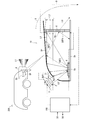
- FIG. 1 is a diagram schematically showing the configuration of a headlamp 10 and a car 200.
- the headlamp 10 includes a laser light source 1, an excitation lens (optical member) 2, a light emitter (optical member) 4, a half parabola mirror (reflecting mirror, optical member) 5P, a base (base, Optical member) 5 h, laser cut filter (optical member) 6, projection lens (optical member) 8, wiring 9, and laser drive circuit 100 at least.
- the automobile 200 is provided with the headlamp 10.
- the headlamp 10 in the head of the motor vehicle 200 so that the half parabola mirror 5P may be located in the perpendicular lower side.
- the front of the car 200 is sufficiently brightly illuminated due to the light-projecting characteristics of the half parabola mirror 5P described later, and light is less likely to be emitted wastefully in the upward direction. It is possible to brighten the light, and it can be expected to obtain preferable light projection characteristics as a headlamp for a car.
- the headlamp 10 may be applied to a traveling headlamp (high beam) for a car or may be applied to a passing headlamp (low beam).
- the laser light source 1 is a light source composed of a single LD chip (semiconductor laser) 11 as shown in FIG. 3 or a plurality of LD chips 11 connected to each other.
- the plurality of LD chips 11 may be connected in series with each other, may be connected in parallel with each other, and may be used in combination of series and parallel.
- the case where the laser light source 1 is formed of a single LD chip 11 and the case (semiconductor laser group) formed of four LD chips 11 connected in series with each other will be described.
- the single LD chip 11 may have a large power of about 5 to 10 W, for example, as a light output of one chip that oscillates a laser beam of 405 nm (blue-violet). Further, as the LD chip 11, one having one light emitting point in one chip (one chip, one stripe) may be used, or one having a plurality of light emitting points (one chip, multiple stripes, or plural chips: for example, 1) Stripes, an assembly of chips with an optical output of 1.0 W, an operating voltage of about 5 V, and a current of about 0.7 A), or individual chips enclosed in a package (stem) You may use two or more things. In this embodiment, it is assumed that the LD chip 11 with a large output (about 5 to 10 W as an optical output) is used with one chip and one stripe.
- the wavelength of the laser beam oscillated by the LD chip 11 is not limited to 405 nm, and is preferably from the near ultraviolet region to the blue region (350 nm or more and 460 nm or less), more preferably from the near ultraviolet region to the blue violet region (350 nm or more and 420 nm or less) What is necessary is just to have a peak wavelength (wavelength of emission peak) in the range.
- the light output of the LD chip 11 is 1 W or more and 20 W or less, and the laser irradiated to the light emitter 4
- the light density of light is preferably 0.1 W / mm 2 or more and 50 W / mm 2 or less. With the light output in this range, it is possible to realize the luminous flux and the luminance required for the headlamp 10 for a vehicle, and to prevent the light emitter 4 from being extremely deteriorated by the high output laser light. That is, a long-life light source can be realized while having high luminous flux and high luminance.
- the phosphor of the light emitter 4 is excellent in heat resistance, for example, when the nanoparticle phosphor described later is used as the phosphor of the light emitter 4, the light density of the laser light irradiated to the light emitter 4 is And may be larger than 50 W / mm 2 .
- the light output of the LD chip 11 or the light of the laser light emitted to the light emitter 4 is not limited to the one using the nanoparticle phosphor described later for the light emitter 4 and it is possible to use one having excellent heat resistance.
- the density may be greater than the above values.
- the light output of the LD chip 11 or the light emitter 4 may be used.
- the light density of the laser beam may be smaller than the above value.
- FIG. 15 shows an example of a simple circuit for driving the LD chip 11
- (b) of FIG. 15 shows the appearance of the LD chip 11 as viewed from the lower right side of the paper surface. .
- the LD chip 11 has a configuration in which a cathode electrode 19, a substrate 18, a cladding layer 113, an active layer 111, a cladding layer 112, and an anode electrode 17 are stacked in this order.
- the substrate 18 is a semiconductor substrate, and it is preferable to use GaN, sapphire, or SiC to obtain blue to ultraviolet excitation light for exciting a phosphor as in the present application.
- III is typically represented by group IV semiconductors such as Si, Ge and SiC, GaAs, GaP, InP, AlAs, GaN, InN, InSb, GaSb and AlN.
- nitride insulator any material of nitride insulator, such as, is used.
- the anode electrode 17 is for injecting a current into the active layer 111 via the cladding layer 112.
- the cathode electrode 19 is for injecting a current from the lower portion of the substrate 18 to the active layer 111 via the cladding layer 113.
- the injection of current is performed by applying a forward bias to the anode electrode 17 and the cathode electrode 19.
- the active layer 111 has a structure in which the cladding layer 113 and the cladding layer 112 are sandwiched.
- a mixed crystal semiconductor made of AlInGaN is used as a material of the active layer 111 and the cladding layer to obtain blue to ultraviolet excitation light.
- a mixed crystal semiconductor mainly composed of Al, Ga, In, As, P, N, and Sb is used as the active layer / cladding layer of the semiconductor laser, and such a configuration may be employed.
- it may be constituted by a II-VI group compound semiconductor such as Zn, Mg, S, Se, Te and ZnO.
- the active layer 111 is a region where light emission occurs due to the injected current, and the emitted light is confined in the active layer 111 due to the difference in refractive index between the cladding layer 112 and the cladding layer 113.
- the active layer 111 is provided with a front side cleavage surface 114 and a rear side cleavage surface 115 provided opposite to each other to confine light amplified by the stimulated emission.
- the front side cleavage surface 114 and the rear side cleavage surface 115 Plays the role of a mirror.
- the active layer 111 may form a multilayer quantum well structure.
- a reflective film (not shown) for laser oscillation is formed on the back side cleavage surface 115 opposite to the front side cleavage surface 114, and the difference in reflectance between the front side cleavage surface 114 and the back side cleavage surface 115 is shown.
- most of the laser light L0 can be irradiated from the light emitting point 116 from the front side cleavage plane 114 which is a low reflectance end face.
- MOCVD metal organic chemical vapor deposition
- MBE molecular beam epitaxy
- CVD chemical vapor deposition
- MOCVD metal organic chemical vapor deposition
- MBE molecular beam epitaxy
- CVD chemical vapor deposition
- the excitation lens 2 is to adjust the area (irradiation area) of the spot of the laser beam L0 irradiated to the light emitter 4. According to the excitation lens 2, the area and position of the spot of the laser beam L 0 irradiated to the light emitter 4 can be adjusted, so that the light emission efficiency of the light emitter 4 and the light projection characteristics of the headlight 10 (direction and intensity distribution of light ) Can be adjusted.
- the lens 2 for excitation makes the area of the spot of laser beam L0 smaller than the area of the surface (light irradiation surface) of the side by which the excitation light of the light-emitting body 4 is irradiated.
- the fluorescence (side emission fluorescence) emitted from the side surface sharing the side with the light irradiation surface of the light emitter 4 is reduced. Therefore, the ratio of the fluorescence emitted from the light irradiation surface of the light emitter 4 to the fluorescence emitted from the entire surface of the light emitter 4 can be increased.
- the material of the lens 2 for excitation can exemplify quartz, for example, it is not limited to this.
- the light emitter 4 generates fluorescence by irradiating the laser light L0 generated from the laser light source 1, and includes a phosphor that emits light upon receiving the laser light L0.
- the light-emitting body 4 is one in which the phosphor is dispersed in the inside of the sealing material, or one in which the phosphor is solidified, and further, one in which these are fixed on a substrate such as metal.
- the light-emitting body 4 is a fluorescent body sealed with a transparent sealing material and fixed on the base 5 h as it is.
- the light emitter 4 can be said to be a so-called wavelength conversion element for converting the laser light L0 into fluorescence, and in the present embodiment, the light emitter 4 is disposed substantially at the focal position of the half parabola mirror 5P.
- the shape of the light emitter 4 is a cylindrical shape (disk shape) having a diameter of a bottom circle of 2 mm, but the size and shape thereof are not limited thereto, and any size and various shapes may be used. It can be selected. As shapes other than a disk shape, prismatic shape, elliptical cylindrical shape, etc. can be illustrated.
- the thickness of the light-emitting body 4 along the irradiation direction of the laser light L0 of the phosphor portion is 1 mm in the present embodiment, but is preferably 0.015 mm to 1.5 mm. If the thickness of the phosphor portion of the light emitter 4 exceeds 1.5 mm, the path length of the transmitted light passing through the light emitter 4 becomes too long, and the efficiency of fluorescence generation in the light emitter 4 decreases. On the other hand, when the thickness of the phosphor portion of the light emitter 4 is less than 0.015 mm, the intensity of the fluorescence generated from the light emitter 4 becomes too weak. However, as long as a desired light emission (fluorescence) light amount can be obtained, the thickness may be outside the above numerical range.
- an oxynitride-based phosphor for example, a sialon phosphor
- a III-V compound semiconductor nanoparticle phosphor for example, indium phosphor: InP
- These phosphors have high heat resistance to the high output (and / or light density) laser light L0 emitted from the LD chip 11, and can suppress the deterioration of the light emitter 4.
- the phosphor of the light emitter 4 is not limited to the one described above, and may be other phosphors such as a nitride-based phosphor.
- the light emitter 4 contains a phosphor selected so that the illumination light L1 is white.
- the selection of the light emitter 4 is specified to the one where the illumination light L1 is white as described above. It is not a thing.
- the sealing material of the light emitting body 4 is, for example, a glass material (inorganic glass, organic-inorganic hybrid glass), or a resin material such as a silicone resin. You may use low melting glass as a glass material.
- the sealing material is preferably one having high transparency, and in the case of high output of laser light, one having high heat resistance is preferable.
- the half parabola mirror 5P reflects the fluorescence generated by the light emitter 4 and forms a light flux (illumination light L1) traveling in a predetermined solid angle.
- the half parabola mirror 5P may be, for example, a member in which a metal thin film is formed on the surface thereof, or may be a member made of metal, or a glass member or synthetic resin transparent to at least the wavelength of fluorescence. It may be of a structure in which the inner surface is covered with the same kind.
- the half parabola mirror 5P is formed of a partial curved surface (half parabola) obtained by cutting the paraboloid of revolution at a plane including the rotation axis.
- the half parabola mirror 5P of such a shape is partially disposed above the upper surface (light irradiation surface) of the light emitter 4 which is larger in area than the side surface. That is, the half parabola mirror 5P is disposed at a position covering the upper surface of the light emitter 4. If it demonstrates from another viewpoint, a part of side surface of the light-emitting body 4 has turned to the direction of the opening part (right side with respect to a paper surface) of the half parabola mirror 5P.
- the fluorescence of the light emitter 4 can be efficiently projected within a predetermined solid angle, and as a result, the utilization efficiency of the fluorescence is achieved. Can be enhanced.
- the half parabola mirror 5P has a half parabola (light reflecting concave SUF3) obtained by cutting the parabola at a plane including the rotation axis, which corresponds to the other half of the parabola.
- structures other than parabola can be arranged.
- the light emitting body 4 can be efficiently cooled by setting the structure as a base 5 h having high thermal conductivity as described later and bringing the light emitting body 4 into contact with the base 5 h.
- the laser light source 1 is disposed outside the half parabola mirror 5P, and the half parabola mirror 5P is formed with a window portion 3 for transmitting or passing the laser beam L0.
- the window 3 is an opening (hole).
- the window 3 is not limited to this, and may include a transparent member capable of transmitting the laser beam L0.
- a transparent plate provided with a filter that transmits the laser light L0 and reflects the fluorescent component of the light emitter 4 may be provided as the window portion 3. In this configuration, it is possible to prevent the fluorescence of the light emitter 4 from leaking from the window 3.
- the reflector included in the headlamp 10 of the present embodiment may include a half parabola mirror having a closed semicircular opening or a part thereof.
- the reflecting mirror is not limited to the half parabola mirror, and can take any form as long as a desired light quantity and intensity distribution can be obtained as illumination.
- the reflecting mirror includes at least a part of a curved surface formed by rotating a figure (elliptic, circle, parabola) about the rotation axis in its reflecting surface. Is more preferable in terms of concentration and light distribution (light intensity distribution).
- the light emitter 4 is supported by the base 5 h, and the base 5 h is configured to reflect a part of the laser light L 0 transmitted through the inside of the light emitter 4.
- the base 5 h is mainly made of metal (for example, copper or iron). Therefore, the base 5 h has high thermal conductivity, and the heat generated by the light emitter 4 can be dissipated efficiently.
- the base 5 h is not limited to one made of metal, and may be a member containing a substance (such as quartz or sapphire) having high thermal conductivity other than metal.
- the surface of the base 5 h in contact with the light emitter 4 preferably functions as a reflective surface when the light emitter 4 does not have a reflective substrate such as metal.
- the said surface is a reflective surface, after the laser beam L0 which injected from the upper surface of the light-emitting body 4 is converted into fluorescence, it can be reflected by the said reflective surface, and can be made to go to the half parabola mirror 5P. Alternatively, the laser beam L0 incident from the upper surface of the light emitter 4 can be reflected by the reflection surface and directed again to the inside of the light emitter 4 to be converted into fluorescence.
- the base 5 h Since the base 5 h is covered by the half parabola mirror 5 P, it can be said that the base 5 h has a surface facing the light reflecting concave surface SUF 3 of the half parabola mirror 5 P. It is preferable that the surface of the base 5h on the side where the light emitter 4 is provided is substantially parallel to the rotation axis of the paraboloid of the half parabola mirror 5P, and that the surface substantially includes the rotation axis.
- the light reflectivity at the portion not in contact with the light emitter 4 of the base 5h is high when the light emission from the light emitter 4 is reflected again and emitted to the outside, and conversely, the fluorescence component of the rereflection is not good. If a necessary light intensity distribution is to be generated, it may be set low. It is conceivable to mirror-polish the surface of the base 5h or to deposit a metal film in order to achieve a high reflectance, and black coating or roughening may be considered to achieve a low reflectance. Alternatively, surface treatment may be performed to selectively absorb the laser beam L0 reflected in an unnecessary direction.
- the laser cut filter 6 is a transparent resin plate that covers the opening of the half parabola mirror 5P.
- the laser cut filter 6 cuts off the coherent component contained in the laser light L0 from the laser light source 1 and generates the incoherent component contained in the laser light and the laser light L0 converted by the light emitter 4 It is preferable to form with the material which permeate
- the laser cut filter 6 absorbs or reflects light having a wavelength shorter than 410 nm to prevent the laser light from leaking to the outside of the apparatus.
- the wavelength of the light cut off by the laser cut filter 6 may be determined in consideration of the color tone of visible light and the wavelength and light amount of the laser light L0.
- the projection lens 8 (front plastic cover) is provided on the opening side (right side with respect to the paper surface) of the half parabola mirror 5P.
- the constituent material of the projection lens 8 is plastic in the present embodiment, but is not limited thereto. For example, other transparent resin materials or quartz may be used.
- the fluorescence generated from the light emitter 4 or the fluorescence reflected by the half parabola mirror 5P is projected to the outside of the half parabola mirror 5P through the projection lens 8.
- the projection lens 8 has a convex lens shape and has a lens function.
- the projection lens 8 may have a concave lens shape as well as the convex lens shape.
- the projection lens 8 does not necessarily have a structure having a lens function, and may have at least a light transmitting property that transmits the fluorescence transmitted through the laser cut filter 6. That is, the projection lens 8 may be made of any material as long as it is at least translucent.
- the thickness of the projection lens 8 is preferably about 3.0 mm or less. This is because when the thickness exceeds 3.0 mm, the absorption of fluorescence can not be ignored, and the cost of the members increases. However, for the purpose of reducing the possibility of breakage due to stepping stones etc., naturally it may be thicker than 3.0 mm in consideration of the absorption of fluorescence and the cost.
- the surface of the projection lens 8 may be covered with a filter (film) that blocks the laser light L0 of the laser light source 1 and transmits the fluorescence generated from the light emitter 4 or the fluorescence reflected by the light reflection concave SUF3. preferable.
- the coherent laser beam L0 transmitted through the light emitter 4 is blocked by the laser cut filter 6 described above.
- the laser cut filter 6 It is also conceivable that the blocking characteristics of the laser beam L0 fluctuate due to temperature and aging, and a part of the laser light L0 leaks. Even in such a case, the laser light L0 can be prevented from leaking to the outside by blocking the laser light L0 by the filter.
- the wiring 9 is a wiring for supplying a current to the laser light source.
- FIG. 1 schematically shows how the wires 9 in the headlamp 10 are routed.
- the wiring on the plus side (solid line part) in the routing of the wiring 9 is directly connected to the laser light source 1.
- the wiring on the minus side (the part indicated by the alternate long and short dash line, the wiring on the reference potential side), that is, a part of the wiring 9 (security wire)
- part of the wiring 9 is part of the wiring on the reference potential side (minus side)
- part of the wiring 9 is on the GND side ( ⁇ body of the vehicle> ground)
- the potential and the potential are connected to the near side or the equal side).
- the part of the wiring 9 and the chassis potential ( ⁇ body> earth potential as a vehicle) are mixed. Is assumed. In the normal use state, the ground potential of the vehicle is considered to be substantially equal to the reference potential of the headlamp 10.
- a part of the wiring 9 is a part of the wiring on the reference potential side, even if another high voltage electrical system approaches the part of the wiring 9 and a discharge or the like occurs, the discharge target is Since it is on the reference potential side of the wiring 9, the possibility of the laser light source 1 being destroyed by an impact due to a discharge or the like can be reduced.
- the excitation lens 2, the light emitter 4, the laser cut filter 6, the half parabola mirror 5 P, and the base 5 h are typical examples of the “optical member”.
- the “optical member” is a member that changes the state of the laser beam L0 emitted from the laser light source 1.
- a prism, a lens, a wavelength conversion element, an optical filter, a diffraction grating, a polarizing plate, an optical path changing member, etc. can be exemplified.
- the “lens” is a member for adjusting the spot diameter of the laser beam, and the excitation lens 2 is a typical example.
- the “wavelength conversion element” is a member that converts laser light into light having different wavelengths.
- the light emitter 4 and a phosphor described later are typical examples, but the wavelength conversion element is not limited to this.
- the second harmonic generation element described above may be used.
- the “optical filter” is a member that blocks light having a wavelength in a predetermined wavelength range and transmits light having a wavelength other than that, and for example, a laser cut filter 6 described later and the above-described filter (film) are typical. It is an example.
- the “light path changing member” is a member that changes the light path of the laser beam L0, and the half parabola mirror 5P and the base 5h are typical examples.
- the headlamp 10 encounters an intentional or accidental accident.
- at least one of the laser light source 1 and the optical member may be deformed or the installation position may be changed. Therefore, the optical path of the laser beam L0 generated from the laser light source 1 may change, or the laser cut filter 6 may not block the laser beam L0, and the laser beam L0 may leak to the outside of the apparatus. .
- the wiring 9 is routed as shown in FIG.
- the wiring 9 is routed as shown in FIG.
- FIG. 2 is a view showing an example of the routing of the wiring 9 in the headlamp 10. As shown in FIG.
- the laser light source 1 and the excitation lens 2 are accommodated in a sealed housing 20 made of a material that does not transmit light. Further, the sealing (wiring) 21 is provided so that disconnection occurs when the sealed housing 20 is broken or opened, and forms a part of the wiring.
- the laser light source 1 is supported by a fixing member 7 a and a fixing member 7 b joined to the inner surface of the sealing housing 20.
- the excitation lens 2 is supported by a fixing member 7 c and a fixing member 7 d joined to the inner surface of the sealing housing 20.
- the light emitter 4 is fixed on the base 5 h by a fixing member 7 e.
- the laser cut filter 6 is fixed on the base 5h by a fixing member 7f.
- the installation method of a part of the wiring 9 is not limited to these cases. That is, a part of the wiring 9 may be installed at a place where it is assumed that there is a possibility that a risk due to the laser beam may occur due to the occurrence of an accident.
- a part of the wiring 9 has a structure in which disconnection easily occurs. Therefore, when at least one of the laser light source 1 and the optical member is deformed or the installation position thereof is changed, the possibility that a part of the wiring 9 is broken can be further enhanced.
- the wiring 9 is a connection portion of conductors made of different materials
- the thickness of a portion of the wiring 9 is thinner than other portions
- a translucent conductive film such as an ITO (indium-tin oxide) film is provided on the surface of the laser light source 1, the excitation lens 2, the light emitter 4, the laser cut filter 6 and the projection lens 8.
- ITO indium-tin oxide
- Do. 1 or 2 shows an example of a portion where a conductive film forming portion (wiring) 9a such as an ITO film is provided in the headlamp 10, but a portion where the conductive film forming portion 9a is provided Is not limited to this example.
- the inner surface SUF 4 closer to the light emitter 4 than the outer surface easily exposed to the air is preferable because it is less susceptible to corrosive gas in the air and the like.
- the conductive film forming portion 9a may be provided on the outer surface as long as the conductive film forming portion 9a is made of a material that is severely degraded by the laser light L0.
- a part of the wiring 9 may be embedded in the adhesive.
- metal foil may be attached between the optical element and the fixing member.
- a part of the wire 9 may be a thin conductor wire or a metal foil may be stretched.
- the laser light source 1 or at least one of the optical members is deformed (damaged) due to an accident or the like, or a shape easily broken when its installation position changes (displacement).
- a pressure sensor or a humidity sensor is used to detect the inflow of external air, but these sensors are special and expensive, but According to the headlamp 10, it is simple and inexpensive because it is sufficient to devise the installation position of a part of the wiring.
- stop of the laser light at the time of an accident occurrence is delayed and dangerous if the mounting position of the air bag sensor is not ahead of the headlight. It is not possible to design independently, which reduces the degree of freedom in design. Further, the probability of the detection of destruction is reduced with respect to a flying object (such as a stepping stone) which penetrates the transparent window (corresponding to the projection lens 8) of the emission surface at high speed only with the acceleration sensor as in the prior art.
- a flying object such as a stepping stone
- the headlamp 10 of the present embodiment it is possible to stop the laser light instantaneously in accordance with the positional deviation or breakage of the optical member, and it is possible to solve these problems. Also, for example, as compared with the case where the laser light source is judged to be on / off after recognizing the state of the wiring and the optical member by a microprocessor etc., if an abnormality such as a positional deviation or breakage of the optical member occurs even when not energized.
- the current supply to the laser light source 1 can be reliably prohibited regardless of the operation of other elements, and the reliability and reliability from the viewpoint of preventing the laser light from being emitted outside the apparatus are high.
- the collision detection unit is provided as described above, and the lighting body is turned off and leakage of the laser is prevented in cooperation with the air bag etc.
- an abnormality occurs.
- the disconnection occurs, the current to the laser light source is physically cut off, so that the special structure as in the document is unnecessary.
- FIG. 14 is a view showing another example of the routing of the wiring 9.
- the routing of the wiring 9 shown in FIG. 14 is different from the routing of the wiring 9 shown in FIG. (1) A point in which two paths of the conduction path (wiring) 9c and the conduction path (wiring) 9d exist in the conduction path to the laser light source 1, and (2) The conduction path 9d is connected to the heat generating conductor 9b.
- the current supply paths to the laser light source 1 are two paths, three or more current supply paths may be provided.
- the conduction path 9c is the same path as the conduction path of FIG. 2 described above, and is connected to the conductive film forming portion 9a. Further, conduction and non-conduction of the conduction path 9c are switched by the conduction path changeover switch 104a.
- the heat-generating conductor 9b is a conductor that generates heat when current flows, and in this embodiment, a thin nichrome wire is adopted.
- the constituent material of the heat-generating conductor 9b is not limited to the nichrome wire.
- the inner surface SUF 4 closer to the light emitter 4 than the outer surface easily exposed to the air is preferable because it is less susceptible to the influence of corrosive gas in the air.
- the heat-generating conductor 9b is made of a substance that is severely degraded by the laser light L0, it may be provided on the outer surface.
- the conduction path 9d is connected to the heat generating conductor 9b. Further, conduction and non-conduction of the conduction path 9d are switched by the conduction path changeover switch 104b.
- FIG. 3 is a block diagram showing an example of the laser drive circuit 100.
- the laser drive circuit 100 includes a laser control unit 101, a laser drive unit 102, and an output switch element 103.
- the laser control unit 101 receives the signal S0 from the illumination control unit 30 installed outside, and returns the signal S4 to the illumination control unit 30.
- the signal S0 is a command signal instructing to turn on (turn on) and turn off (turn off) the laser light source 1, and a command signal to instruct the drive voltage and drive current of the laser light source 1 respectively.
- the signal S4 is a condition report signal including the lighting condition of the laser light source 1 and an abnormality such as a failure.
- the laser drive unit 102 receives the signal S1 from the laser control unit 101, and returns the signal S3 to the laser control unit 101.
- the signal S1 is a control signal that controls lighting (ON) and extinguishing (OFF) of the laser light source 1, and a control signal that indicates the magnitude of each of the driving voltage and the driving current.
- the signal S3 is a status report signal that reports the status of the laser drive unit 102, reports the drive current of the laser light source 1, and reports the drive voltage of the laser light source 1.
- the laser drive unit 102 receives the signal S1 from the laser control unit 101, and supplies the power from the power source E (battery) to the laser light source 1 as a drive voltage and a drive current.
- the laser light source 1 is turned on with the drive voltage and drive current supplied from the laser drive circuit 100.
- the output switch element 103 is provided, as described later, since the laser drive unit 102 is often provided with a capacitor such as the capacitor 1023, the collision acceleration is detected by an acceleration sensor not shown. It is desirable to provide for shortening the turn-off time of the laser light source 1 in the case where an abnormality is detected in the laser drive unit 102 or the like.
- the control of the output switch element 103 is performed by at least one of the laser control unit 101 and the laser drive unit 102. Further, the signal S2 is a control signal for controlling ON and OFF of the output switch element 103.
- the laser drive unit 102 is configured in accordance with the connection form of the plurality of LD chips 11 in the laser light source 1.
- Examples 1 to 10 of the laser drive unit 102 will be described.
- the laser drive units 102 in the first to tenth embodiments described below are all applicable to the laser drive circuit 100 shown in FIG. Descriptions of configurations other than the configurations described in the following specific embodiments may be omitted as necessary. However, in the case where other embodiments are described, the configurations are the same as the configurations. Moreover, about the member which has the function same as the member shown to each Example for convenience of explanation, the same code
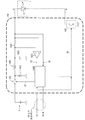
- FIG. 4 is a block diagram showing a circuit configuration of the laser driving unit 102 (step-up type) of the first embodiment. This is an example of a step-up type circuit used when the voltage required to drive the laser light source 1 is higher than the voltage of the power supply E.
- the laser driving unit 102 according to the first embodiment is used when the laser light source 1 includes a plurality of LD chips 11 and is connected in series (3 to 4 or more in series).
- a main switch element 105 As shown in FIG. 4, a main switch element 105, a coil 1021, a diode 1022, a current detection resistor 1024, a differential amplifier 1025, a switching control unit 1026, and the output switch element 103 described above are provided. Note that one end of the coil 1021 is connected to the power supply E. Note that another switch element may be provided between the power source E and the coil 1021.
- the laser drive unit 102 of the first embodiment is connected to the laser light source 1 including a total of four LD chips 11.
- the switching control unit 1026 receives the signal S1 from the laser control unit 101, and returns the signal S3 to the laser drive unit 102.
- the signal S1 and the signal S3 are as described above. Further, the switching control unit 1026 receives the signal S1 and switches between conduction (ON) and non-conduction (OFF) of the main switch element 105 so that the (desired) current instructed to the laser light source 1 flows.
- the main switch element 105 While the main switch element 105 is ON, the current from the power source E is stored as magnetic flux energy through the coil 1021 and as charge in the capacitor C. During this time, a current is supplied from the capacitor 1023 to the laser light source 1.
- the current supplied to the laser light source 1 is detected by the current detection resistor 1024 and the differential amplifier 1025, and the main switch element 105 is turned ON / OFF so as to maintain the drive current value instructed from the laser control unit 101.
- the signal S5 shown in FIG. 4 is an output current signal
- the signal S6 is an output voltage signal
- the signal S7 is a control signal for controlling the switching of the main switch element 105 between ON and OFF.
- the output switch element 103 may be configured to interrupt the current forcibly (at high speed).
- the current to the laser light source 1 can be immediately and surely interrupted regardless of the operation of other elements by breakage of a part of the wiring 9 (security wire). Not to mention.
- the portion indicated by the broken line in the wiring 9 is used as a security wire, that is, the laser light source 1, the excitation lens 2, the light emitter 4, the half parabola mirror 5 P, and the base 5 h, the laser cut filter 6, the fixing members 7 a to 7 f, and the surface of the sealing housing 20 or in the vicinity thereof, and the seal 21.
- FIG. 5 is a block diagram showing a circuit configuration of the laser driving unit 102 (step-up type) of the second embodiment.
- the laser driving unit 102 of the second embodiment differs from the first embodiment in the laser light source 1, the excitation lens 2, the light emitter 4, the half parabola mirror 5P, the metal base 5h, the laser cut filter 6, and the fixing members 7a to 7f. And, the surface of the sealing housing 20 or its vicinity, and a part (security wire) of the wiring 9 leading to the seal 21 are the part shown by the broken line (wiring on the reference potential side).
- the laser light source 1 can be prevented from being damaged because an excessive current or voltage in the forward or reverse direction is not applied to the laser light source 1.
- the laser light source 1 is turned off in an emergency such as an accident, it is desirable to prevent the leakage of the laser light by turning off the output switch element 103 prior to stopping the laser drive unit 102. .
- the laser is immediately and surely ensured by a part of the wiring 9 (security wire) regardless of the operation of the output switch element 103 or the like. It goes without saying that current interruption to the light source 1 is possible.
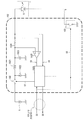
- FIG. 6 is a block diagram showing the circuit configuration of the laser drive unit 102 (step-down type) of the third embodiment. This is an example of a step-down circuit used when the voltage required to drive the laser light source 1 is lower than the voltage of the power supply E.
- the laser driving unit 102 according to the third embodiment is used when the number of LD chips 11 included in the laser light source 1 in series is small.
- a main switch element 105 As shown in FIG. 3, a main switch element 105, a coil 1021, a diode 1022, a current detection resistor 1024, a differential amplifier 1025, a switching control unit 1026, and the output switch element 103 described above are provided. Note that one end of the coil 1021 is connected to the power supply E. Note that another switch element may be provided between the power source E and the coil 1021.
- the laser drive unit 102 of the third embodiment is connected to the laser light source 1 including the single LD chip 11.
- the switching control unit 1026 receives the signal S1 from the laser control unit 101, and returns the signal S3 to the laser drive unit 102.
- the signal S1 and the signal S3 are as described above. Further, the switching control unit 1026 receives the signal S1 and switches between conduction (ON) and non-conduction (OFF) of the main switch element 105 so that the (desired) current instructed to the laser light source 1 flows. .
- the main switch element 105 While the main switch element 105 is ON, the current from the power source E is stored as magnetic flux energy through the coil 1021 and as a charge in the capacitor 1023, and the current is also supplied to the laser light source 1 as well.
- the current supplied to the laser light source 1 is detected by the current detection resistor 1024 and the differential amplifier 1025, and the main switch element 105 is turned ON / OFF so as to maintain the drive current value instructed from the laser control unit 101.
- the magnetic flux energy of the coil 1021 is supplied to the laser light source 1 through the diode 1022 and the capacitor 1023.
- the capacitor 1023 performs a smoothing operation for reducing the fluctuation of the voltage (current) to the laser light source 1 by switching the main switch element 105 between ON and OFF.
- the signal S6 output voltage signal
- the signal S6 is used to monitor whether or not a voltage according to an instruction from the laser control unit 101 is output.
- the main switch element 105 is turned off to lower the output voltage, assuming that the laser light source 1 has an open failure or that the laser drive unit 102 has a failure. Used for
- breakage of a part of the wiring 9 immediately ensures the laser light source 1 regardless of the operation of other elements. It is possible to interrupt the current.
- FIG. 7 is a block diagram showing a circuit configuration of the laser driving unit 102 (step-down type) of the fourth embodiment.
- the laser driving unit 102 of the fourth embodiment differs from the third embodiment in the laser light source 1, the excitation lens 2, the light emitter 4, the half parabola mirror 5P, the base 5h, the laser cut filter 6, the fixing members 7a to 7f, And, the surface of the sealing housing 20 or its vicinity, and a part (security wire) of the wiring 9 leading to the seal 21 are the part (wiring on the reference potential side) indicated by the broken line.
- breakage of a part of the wiring 9 immediately ensures the laser light source 1 regardless of the operation of other elements. It is possible to interrupt the current.
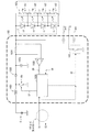
- FIG. 8 is a block diagram showing a circuit configuration of the laser driving unit 102 (step-up type) of the fifth embodiment.
- the laser driving unit 102 differs from the second embodiment in that four bypass current paths bp for bypassing respective poles of four LD chips 11 constituting the laser light source 1 and four bypass current paths bp.
- the bypass switch element 106 is provided for each of the two.
- the four bypass switch elements 106 are collectively referred to as a bypass switch element group 106 a.
- the laser control unit 101 sends a drive stop (boost stop) instruction to the switching control unit 1026 to turn on the bypass switch element group 106a.
- the output switch element 103 when the output switch element 103 is turned off for emergency light off, even if the laser light source 1 is not broken, the parasitic inductance pa1 continues to flow the current to prevent the off (light off) from being delayed. It is for. If the output switch element 103 has a sufficient withstand voltage, the laser light source 1 will not be damaged even if the counter electromotive voltage pa2 is generated, and the light-off will not be delayed. However, even if the output switch element 103 can not withstand this voltage and breaks down (breaks down) to become conductive, the bypass switch group 106a is turned on in synchronization with turning off or prior to turning off. In this case, neither damage to the laser light source 1 nor delay in turning off occurs.
- the output switch element 103 is provided to perform pulse driving of the laser light source 1 and the ON and OFF operations are performed.
- the bypass switch element group 106a has the same timing as the output switch element 103 is turned off, or the driving from the laser control unit 101 is stopped. Keep turning OFF according to the instruction of (Boosting stop).
- the output switch element and the bypass switch element group 106a may be switched ON and OFF substantially in synchronization.
- the bypass switch element group 106a can also be used if it is provided as the bypass current path bp at the time of an open failure, in which case no additional component is required.
- bypass current path bp and the bypass switch element 106 are separately provided on both electrodes of each LD chip 11 as in the laser drive unit 102 of the present embodiment if only protection from surge is intended.
- all of the plurality of LD chips 11 included in the laser light source 1 are at least one of the group consisting of only a single LD chip 11 and the group consisting of two or more LD chips 11 connected to each other. Now, consider a plurality of groups of LD chips 11 that are the result of grouping.
- bypass switch element group 106a switches the conduction and non-conduction of the plurality of bypass current paths bp for bypassing the respective poles of the plurality of LD chips 11 and the plurality of bypass current paths bp.
- the element 106 may be provided.
- a group of two or more LD chips 11 connected to each other is a group of two or more LD chips 11 when two or more LD chips 11 are connected to each other only in series connection. However, this includes both the case where they are connected to each other only by parallel connection, and the case where two or more LD chips 11 are connected to each other in a state in which serial connection and parallel connection are mixed.
- both poles of the LD chip 11 group are paths connecting the plurality of LD chips 11 included in the group. Among these, it becomes the terminal of the both ends of the route where connection number of LD chip 11 becomes maximum.
- the bypass switch element group 106 a is provided outside the laser drive unit 102, but may be provided inside the laser drive unit 102.
- the entire short circuit operation of the bypass switch element group 106a is performed earlier than the output switch element 103 (direct shutoff switch) and later than the operation stop of the laser drive circuit 100. It is preferable to open the shorting operation after the same timing as turning on the direct cutoff switch until the laser drive circuit 100 starts up, but the timing is not limited to these as long as no damage occurs to each element or circuit. .
- breakage of a part of the wiring 9 immediately ensures the laser light source 1 regardless of the operation of other elements. It is possible to interrupt the current.
- FIG. 9 is a block diagram showing a circuit configuration of the laser driving unit 102 (step-up type) of the sixth embodiment.
- the laser driving unit 102 of the sixth embodiment is different from that of the second embodiment in that a (minus) clamping diode is used with the direction from the reference potential point P toward the terminal T on the reference potential side of the laser light source 1 as a forward direction. (A selectively conductive element) 1027 is provided.
- a part of the wiring 9 uses the wiring on the side of the reference potential of the laser light source 1 (the part indicated by the broken line). Therefore, if the wiring 9 is temporarily cut off, the laser light source 1 is naturally turned off, but in this state, the wiring 9 on the reference potential side (GND side) of the laser light source 1 has a mixed feeling as shown in the fifth embodiment.
- the clamp diode 1027 prevents the application of an excessive current or voltage to the laser light source 1 even if there is a collision with a voltage lower than the reference potential, so destruction of the laser light source 1 and unnecessary light emission ) Can be prevented. This is a new effect that occurs in addition to that shown in the previous embodiment.
- the clamping diode 1027 As a secondary effect, due to the presence of the clamping diode 1027, for example, when the output switch element 103 is turned off, the back electromotive voltage pa2 generated by the parasitic inductance pa1 exceeds the withstand voltage of the output switch element 103 and breaks down ( Also in the case of conduction, the current path around the clamping diode 1027 serves as a current path for the back electromotive voltage pa2 to take over the unexpected current to the laser light source 1, thereby breaking the laser light source 1 Can be prevented.
- breakage of a part of the wiring 9 immediately ensures the laser light source 1 regardless of the operation of other elements. It is possible to interrupt the current.
- FIG. 10 is a block diagram showing a circuit configuration of a laser driving unit 102 (step-up type) according to a seventh embodiment.
- the laser driving unit 102 of the seventh embodiment differs from that of the second embodiment in that the (plus) clamping diode (first) has a forward direction from the terminal T on the reference potential side of the laser light source 1 toward the reference potential point P. And the point where the output switch element 103 is eliminated.
- the (plus) clamping diode 1027 serves as a forward current path for the laser light source 1. Therefore, when the laser drive unit 102 is driving the laser light source 1, a current path is formed regardless of ON / OFF of the output switch element 103 as provided in the previous embodiment, and the laser light source is formed. 1 continues to emit light. Therefore, unlike the fifth embodiment and the sixth embodiment, for example, the output switch element 103 need not be provided in this embodiment.
- the problem does not occur at first if the other party is the chassis potential (ground potential) of the vehicle as described above. If the voltage on the other side that is mixed with the part indicated by is a voltage higher than the reference potential, such as the power supply voltage, a voltage in the reverse direction is applied to the laser light source 1, and the laser light source 1 may be damaged.
- the LD chip 11 is considerably weaker in reverse voltage than the forward voltage required for normal lighting.
- the (plus) clamping diode 1027 is effective and leads the surge voltage to the GND and the laser light source Protect one.
- the (plus) clamp diode may of course be used in combination with the minus clamp diode.
- FIG. 11 is a block diagram showing a circuit configuration of the laser driving unit 102 (step-up type) of the eighth embodiment.
- the laser driving unit 102 of the eighth embodiment differs from that of the sixth embodiment (or the seventh embodiment) in the switch element for preventing abnormal voltage between the terminal T on the reference potential side of the laser light source 1 and the reference potential point P. (Second selective conduction element) 1028 is provided.
- the abnormal voltage preventing switch element 1028 is a time when a negative voltage surge is generated on the GND side of the laser light source 1 as in the sixth or seventh embodiment (ie, the laser light source 1 is turned off, the output switching element 103). Turn on (turn on) with. Similar to the sixth embodiment, in the sixth embodiment, although the voltage after clamping remains by the forward voltage of the clamping diode 1027, the sixth embodiment is basic in the present embodiment using the abnormal voltage protection switch element 1028. Only the ON resistance of the abnormal voltage prevention switch element 1028 can be seen, and the forward voltage can be regarded as almost zero although it depends on the amount of surge current. Therefore, the clamp (surge suppression) is excellent.
- the switch element 1028 for preventing abnormal voltage of this embodiment is a laser light source. I can not protect one. Therefore, it is still more desirable in this case to combine the abnormal voltage preventing switch element 1028 with the (plus) clamping diode 1027 shown in the previous embodiment. In the combination, for example, it is preferable to provide the bypass path switch 106 a in the fifth embodiment instead of the output switch element 103 as described above.
- the above embodiment In addition, in order to protect the laser light source 1 from the interaction with a negative surge (counter electromotive voltage pa2) or a voltage lower than the reference potential due to the parasitic inductance pa1 of a part (the broken line portion) of the wiring 9, the above embodiment Of course, it may be used in combination with the six (minus) clamp diodes 1027.
- breakage of a part of the wiring 9 immediately ensures the laser light source 1 regardless of the operation of other elements. It is possible to interrupt the current.
- FIG. 12 is a block diagram showing a circuit configuration of a laser driving unit 102 (step-up type) according to a ninth embodiment.
- the laser driving unit 102 of the eighth embodiment is different from that of the fifth embodiment in that a bypass resistance r is provided in series with the bypass switch element 106 in each of the bypass current paths bp in the bypass switch element group 106a. Only.
- the bypass switch element is referred to as 107, and the group is referred to as 107a.
- the reason for providing the bypass resistance r will be described.
- the laser control unit 101 sends a drive stop (boost stop) instruction to the switching control unit 1026 to turn on the bypass switch element group 107a. Since the output of the laser drive unit 102 is not directly short-circuited by the bypass switch device 106 even if the bypass switch element group 107a is turned on while the laser drive unit 102 is still performing the output (drive) operation, bypassing It is possible to perform the ON timing of the switch element group 107a earlier than the operation stop timing of the laser drive unit 102.
- both ends of the LD chip group 11 can be shorted prior to the current OFF to the laser light source 1 (including the one due to the output switch element 103 being OFF), and the protection effect of the LD chip 11 is enhanced. Since it becomes an alternative current path for (back electromotive force), the turn-off can be speeded up.
- the output of the laser drive unit 102 is connected to the reference potential GND through the resistor included in the inside through the bypass switch element group 107a at any time of laser on / off, and the output of the laser drive unit 102 is directly GND. Since the diode 1022 and the coil 1021 are not short circuited directly, for example, it is possible to eliminate the possibility that the excessive current may flow to damage.
- the exact timing of switching control of the bypass switch element group 107a is not required either, and it is turned off after the operation of the laser drive circuit 102 starts (the operation for turning on the laser light source 1 starts) and similarly stopped (the light of the laser light source 1 is turned off) Turn on before) and control is easy.
- the bypass switch element group 107a can also be used as a bypass current path if it is provided as a bypass current path in case of an open failure, in which case no additional parts are needed.
- the bypass resistance r may be, for example, a connection configuration in which a part of the heat generating conductor 9 b described in FIG. 14 is separated.
- the bypass switch element 107 is turned on, the number of laser chips 11 to be lit is reduced, but if the laser light source 1 does not need to be lit, for example, it contributes to the anti-fog protection as a heater during stopping.
- the LD chip 11 breaks down, the amount of power consumption for that portion can be used for antifogging, so it will be released compared with a simple resistor that emits heat. Leads to the effective use of power.
- breakage of a part of the wiring 9 immediately ensures the laser light source 1 regardless of the operation of other elements. It is possible to interrupt the current.
- FIG. 13 is a block diagram showing the circuit configuration of the laser drive unit 102 of the tenth embodiment.
- Example 10 shows an example of a circuit configuration where the reference potential side is not the negative electrode side of the power source E but the positive electrode side.
- the switching control unit 1026 receives the signal S1 from the laser control unit 101, and returns the signal S3 to the laser drive unit 102.
- the signal S1 and the signal S3 are as described above. Further, the switching control unit 1026 receives the signal S1 and switches between conduction (ON) and non-conduction (OFF) of the main switch element 105 so that the (desired) current instructed to the laser light source 1 flows. .
- the main switch element 105 While the main switch element 105 is ON, the current from the power source E is stored as magnetic flux energy through the coil 1021 and as charge in the capacitor 1023. During this time, a current is supplied from the capacitor 1023 to the laser light source 1.
- the current supplied to the laser light source 1 is detected by the current detection resistor 1024 and the differential amplifier 1025, and the main switch element 105 is turned ON / OFF so as to maintain the drive current value instructed from the laser control unit 101.
- point (A) in the figure acts as a part of the wiring 9 (security wire). Also, point (B) is one end when connecting a diode or switch element (clamping diode 1027 or switch element 1028 for preventing abnormal voltage) for preventing surge or collision, and the reference potential (GND of the laser drive circuit 100) ) And the element (C).
- Examples 1 to 10 show that both the positive side and the negative side of the power source E (battery) can be handled as the reference potential as GND, the entire laser drive circuit 100 including the power source E is shown as an extreme example. Can be electrically floated from the chassis of the automobile including the laser light source 1. In this case, the connection destination of one end of the previously described element for preventing surge or interaction (clamping diode 1027 or switch element 1028 for preventing abnormal voltage) is not GND, but the potential on the positive side of power source E (on wiring 9e It becomes a dashed line part).
- either the positive side or the negative side of the power source E can be constructed as the reference potential, or it can be completely floating, so the degree of freedom in circuit design is increased and the laser at the time of breakage is achieved with both plus and minus ground configurations. It can function to prevent light leakage.
- breakage or breakage of the optical member is caused by breakage of a part of the wiring 9 (security wire) regardless of the ON / OFF of the bypass switch group 106 a or the output switch 103. It is possible to interrupt the current to the laser light source 1 immediately and surely regardless of the operation of other elements.
- the light emitting device of the present invention as a method of installing a part of the above wiring, (1) When a part of the wiring is installed at or near the surface of at least one of the laser light source and the optical member, (2) A portion of the wiring can be provided on the surface of the fixing member for fixing at least one of the laser light source and the optical member or in the vicinity thereof.
- the installation method of a part of wiring is not limited to these cases. That is, a part of the wiring may be installed at a place where it is assumed that there is a possibility that a risk due to the laser beam may occur due to the occurrence of an accident.
- a part of the wiring may be easily broken.
- the possibility of disconnection of a part of the wiring can be further enhanced.
- a portion of the wiring is a connection portion of a conductor made of a different material, or when the thickness of a portion of the wiring is smaller than that of the other portion, or It is conceivable that, for example, a part of the wiring is shaped to easily cause disconnection.
- a part of the wiring may be a part of the wiring on the reference potential side.
- the light emitting device further includes a bypass current path bypassing both electrodes of the laser light source, and a bypass switch element switching between conduction and non-conduction of the bypass current path, wherein the bypass switch element is the laser When the light source is turned off, the bypass current path may be made conductive.
- the laser light source is composed of a plurality of semiconductor lasers connected to each other, and all of the plurality of semiconductor lasers included in the laser light source are a group consisting of only a single semiconductor laser, A plurality of bypass current paths for bypassing respective poles of a plurality of semiconductor laser groups, which are a result of grouping in at least one group of two or more semiconductor lasers connected to each other; A plurality of bypass switch elements for switching between conduction and non-conduction of the bypass current paths may be provided, and the bypass switch elements may conduct the bypass current paths when the laser light source is turned off.
- the parasitic inductance increases with the length of the wire, the longer the wire, the larger the parasitic inductance. Therefore, when the wiring lengthens, a large surge (a sudden change in voltage or current) may occur due to parasitic inductance when the laser light source is turned off, and the laser light source may be destroyed. In addition, when the laser light source is turned off, there is a possibility that the parasitic inductance continues to flow the current to the laser light source to delay the turn-off.
- the bypass switch element causes the bypass current path to conduct when the laser light source is turned off.
- the following cases (1) to (3) can be considered.
- a group of two or more semiconductor lasers connected to each other may be connected to each other only by parallel connection when two or more semiconductor lasers are connected to each other only by series connection. And in the case where two or more semiconductor lasers are connected to each other in a state in which serial connection and parallel connection are mixed.
- both poles of the semiconductor laser group are semiconductors among paths connecting a plurality of semiconductor lasers included in the group. It becomes a terminal of the both ends of the path
- the terminal on the reference potential side of the laser light source when the potential of the terminal on the reference potential side of the laser light source is higher or lower than the potential of the reference potential point, the terminal on the reference potential side and the reference potential are selectively selected.
- a first selective conduction element may be provided which conducts between the point.
- the first selectively conducting element is selectively switched to the reference potential side when the potential of the terminal on the reference potential side of the laser light source is higher or lower than the potential of the reference potential point. Conduction is made between the terminal and the reference potential point.
- the light emitting device of the present invention may further include a second selective conduction element that selectively conducts at a predetermined timing between the reference potential side terminal of the laser light source and the reference potential point.
- the second selectively conducting element selectively conducts between the terminal on the reference potential side of the laser light source and the reference potential point at a predetermined timing.
- the "predetermined timing” is, for example, a timing (time point) which is predetermined in anticipation of a time point when a large surge occurs on the reference potential side of the laser light source (at the time of turning off the laser light source, etc.).
- the second selectively conducting element can suppress (clamp) the surge regardless of the potential of the terminal on the reference potential side of the laser light source, the second selectively conducting element can be clamped in terms of clamping rather than the first selectively conducting element. Excellent.
- a lighting device and a headlight including the light emitting device described above, and a vehicle including the headlight may be configured.
- the present invention can be applied to a light emitting device, a lighting device and a headlight provided with the light emitting device, and a vehicle provided with the headlight.
- a lighting apparatus or headlight
- it can apply not only to a vehicle headlamp but other lighting apparatuses (or headlight).
- a downlight can be mentioned as an example of other lighting devices (or headlights).
- the downlight is a lighting device installed on the ceiling of a structure such as a house or a vehicle.
- the lighting device (or the headlamp) of the present invention may be realized as a headlamp of a moving object other than a vehicle (for example, a person, a ship, an aircraft, a submersible, a rocket, etc.) It may be realized as a searchlight, a projector, a room lighting fixture (such as a stand lamp) other than a downlight, and an outdoor lighting fixture.
Landscapes
- Physics & Mathematics (AREA)
- Engineering & Computer Science (AREA)
- General Engineering & Computer Science (AREA)
- Optics & Photonics (AREA)
- Spectroscopy & Molecular Physics (AREA)
- Condensed Matter Physics & Semiconductors (AREA)
- General Physics & Mathematics (AREA)
- Electromagnetism (AREA)
- Non-Portable Lighting Devices Or Systems Thereof (AREA)
- Lighting Device Outwards From Vehicle And Optical Signal (AREA)
- Semiconductor Lasers (AREA)
Abstract
Description
本願出願人により出願された先願〔特願2009-237076号(2009年10月14日出願);特開2011-86432号公報(2011年04月28日公開)〕に記載の照明装置では、蛍光体部材からの反射光を検出する光センサや、衝突を検出する加速度センサを設け、これらの検出結果に基づき、LDへの通電を遮断している。
まず、図1に基づき、本発明の一実施形態であるヘッドランプ(発光装置,照明装置,前照灯)10および自動車(車両)200の構成について説明する。図1は、ヘッドランプ10および自動車200の構成を概略的に示す図である。図1に示すように、ヘッドランプ10は、レーザ光源1、励起用レンズ(光学部材)2、発光体(光学部材)4、ハーフパラボラミラー(反射鏡,光学部材)5P、ベース(基台,光学部材)5h、レーザカットフィルタ(光学部材)6、投影レンズ(光学部材)8、配線9、および、レーザ駆動回路100を少なくとも含む。
レーザ光源1は、図3に示すように単一のLDチップ(半導体レーザ)11からなる、または、互いに接続された複数のLDチップ11からなる光源である。
次に、図15に基づき、LDチップ11のより具体的な構造について説明する。
再び図1および図2に戻って説明を続ける。励起用レンズ2は、発光体4に照射されるレーザ光L0のスポットの面積(照射面積)を調整するものである。励起用レンズ2によれば、発光体4に照射されるレーザ光L0のスポットの面積および位置を調整できるので、発光体4の発光効率やヘッドライト10の投光特性(光の方向や強度分布)を調整することができる。
発光体4は、レーザ光源1から発生したレーザ光L0を照射することにより蛍光を発生するものであり、レーザ光L0を受けて発光する蛍光体を含んでいる。具体的には、発光体4は、封止材の内部に蛍光体が分散されているもの、または、蛍光体を固めたもの、更にはこれらを金属などの基板上に固定させたものである。本実施形態では発光体4は、蛍光体を透明な封止材で封止し、それをそのままベース5h上に固定しているものを想定している。
ハーフパラボラミラー5Pは、発光体4が発生させた蛍光を反射し、所定の立体角内を進む光線束(照明光L1)を形成する。このハーフパラボラミラー5Pは、例えば、金属薄膜がその表面に形成された部材であってもよいし、金属製の部材であっても、あるいは少なくとも蛍光の波長に対して透明なガラス部材や合成樹脂類で内面が被覆された構造のものであってもよい。
本実施形態では、発光体4が、ベース5hによって支持されており、ベース5hは、発光体4の内部を透過するレーザ光L0の一部を反射するようになっている。
レーザカットフィルタ6は、ハーフパラボラミラー5Pの開口部を覆う透明な樹脂板である。レーザカットフィルタ6は、レーザ光源1からのレーザ光L0に含まれるコヒーレントな成分を遮断するとともに、当該レーザ光に含まれるインコヒーレントな成分と、発光体4においてレーザ光L0を変換することにより生成された白色光とを透過する材質で形成されることが好ましい。
投影レンズ8(前面プラスチックカバー)は、ハーフパラボラミラー5Pの開口部側(紙面に対して右側)に設けられている。投影レンズ8の構成材料は、本実施形態では、プラスチックであるが、これに限定されない。例えば、その他の透明な樹脂材料や石英などであっても良い。
配線9は、レーザ光源に電流を供給するための配線である。図1は、ヘッドランプ10における配線9の引き回しの様子を概略的に示している。
次に、図2に基づき、配線9の引き回しについてより詳細に説明する。図2は、ヘッドランプ10における配線9の引き回しの一例を示す図である。
(1)配線9の一部をレーザ光源1および光学部材の少なくとも一方の表面またはその近傍に設置する場合、および、
(2)配線9の一部を、レーザ光源1および光学部材の少なくとも一方を固定するための固定部材7a~7fの表面またはその近傍に設置する場合、
などを例示することができる。
次に、図14に基づき、ヘッドランプ10における配線9の引き回しの他の一例について説明する。図14は、配線9の引き回しの他の一例を示す図である。
(1)レーザ光源1への通電経路に通電経路(配線)9cおよび通電経路(配線)9dの2経路が存在している点、および、
(2)通電経路9dが、発熱性導電体9bに接続されている点である。
通電経路9cは、上述した図2の通電経路と同一の経路であり、導電膜形成部9aに接続される。また、通電経路9cの導通および非導通は、通電経路切替えスイッチ104aによって切替られる。
次に、発熱性導電体9bは、電流が流れると熱を発生する導電体であり、本実施形態では、細いニクロム線を採用している。しかしながら、発熱性導電体9bの構成材料としては、ニクロム線に限定されない。
通電経路9dは、発熱性導電体9bに接続される。また、通電経路9dの導通および非導通は、通電経路切替えスイッチ104bによって切替られる。
次に、図3に基づき、ヘッドランプ10におけるレーザ駆動回路100の概要構成について説明する。まず、図3は、レーザ駆動回路100の一例を示すブロック図である。同図に示すように、レーザ駆動回路100は、レーザ制御部101、レーザ駆動部102、および、出力スイッチ素子103を備える。
次に、図4~13に基づき、レーザ駆動部102の実施例1~10について説明する。なお、以下で説明する実施例1~10のレーザ駆動部102は、いずれも図3に示すレーザ駆動回路100に適用可能なものである。以下の特定の実施例で説明する構成以外の構成については、必要に応じて説明を省略する場合があるが、他の実施例で説明されている場合は、その構成と同じである。また、説明の便宜上、各実施例に示した部材と同一の機能を有する部材については、同一の符号を付し、適宜その説明を省略する。
図4は、実施例1のレーザ駆動部102(昇圧型)の回路構成を示すブロック図である。レーザ光源1の駆動に必要な電圧が、電源Eの電圧よりも高い場合に用いられる昇圧型の回路の一例である。なお、実施例1のレーザ駆動部102は、レーザ光源1が、複数のLDチップ11を備え、やや多めに直列接続(直列数3~4またはそれ以上)されている場合に用いられる。
次に、図5は、実施例2のレーザ駆動部102(昇圧型)の回路構成を示すブロック図である。
図6は、実施例3のレーザ駆動部102(降圧型)の回路構成を示すブロック図である。レーザ光源1の駆動に必要な電圧が、電源Eの電圧よりも低い場合に用いられる降圧型の回路の一例である。なお、実施例3のレーザ駆動部102は、レーザ光源1に含まれるLDチップ11の直列数が少ない場合に用いられる。
次に、図7は、実施例4のレーザ駆動部102(降圧型)の回路構成を示すブロック図である。
次に、図8は、実施例5のレーザ駆動部102(昇圧型)の回路構成を示すブロック図である。
(1)複数のLDチップ11群のすべてが、単一のLDチップ11のみからなる群である場合。
(2)複数のLDチップ11群のすべてが、2以上のLDチップ11からなる群である場合。
(3)複数のLDチップ11群のうち、一部のLDチップ11が、単一のLDチップ11のみからなる群であり、かつ、その他のLDチップ11群が、2以上のLDチップ11からなる群である場合。
次に、図9は、実施例6のレーザ駆動部102(昇圧型)の回路構成を示すブロック図である。
次に、図10は、実施例7のレーザ駆動部102(昇圧型)の回路構成を示すブロック図である。
次に、図11は、実施例8のレーザ駆動部102(昇圧型)の回路構成を示すブロック図である。
次に、図12は、実施例9のレーザ駆動部102(昇圧型)の回路構成を示すブロック図である。
次に、図13は、実施例10のレーザ駆動部102の回路構成を示すブロック図である。実施例10は、基準電位側が電源Eの負極側ではなく正極側である場合の回路構成の一例を示す。
また、本発明は、以下のように表現しても良い。
(1)配線の一部をレーザ光源および光学部材の少なくとも一方の表面またはその近傍に設置する場合、
(2)配線の一部を、レーザ光源および光学部材の少なくとも一方を固定するための固定部材の表面またはその近傍に設置する場合などを例示することができる。
(1)複数の半導体レーザ群のすべてが、単一の半導体レーザのみからなる群である場合。
(2)複数の半導体レーザ群のすべてが、2以上の半導体レーザからなる群である場合。(3)複数の半導体レーザ群のうち、一部の半導体レーザ群が、単一の半導体レーザのみからなる群であり、かつ、その他の半導体レーザ群が、2以上の半導体レーザからなる群である場合。
なお、本発明は上述した実施形態に限定されるものではなく、請求項に示した範囲で種々の変更が可能である。すなわち、請求項に示した範囲で適宜変更した技術的手段を組み合わせて得られる実施形態についても本発明の技術的範囲に含まれる。また、上記発明を実施するための形態の異なる箇所にそれぞれ開示された技術的手段を適宜組み合わせて得られる実施形態についても本発明の技術的範囲に含まれる。
2 励起用レンズ(光学部材)
3 窓部
4 発光体(光学部材)
5P ハーフパラボラミラー(反射鏡,光学部材)
5h ベース(光学部材)
6 レーザカットフィルタ(光学部材)
7a~7f 固定部材
8 投影レンズ(光学部材)
9 配線
9a 導電膜形成部(配線)
9b 発熱性導電体(配線)
9c,9d 通電経路(配線)
10 ヘッドランプ(発光装置,照明装置,前照灯)
11 LDチップ(半導体レーザ)
20 密閉筺体(固定部材)
21 封印(配線)
30 照明制御部
100 レーザ駆動回路
101 レーザ制御部
102 レーザ駆動部
103 出力スイッチ素子
104a,104b 通電経路切替えスイッチ
105 主スイッチ素子
106 バイパススイッチ素子
106a バイパススイッチ素子群
107 バイパススイッチ素子
107a バイパススイッチ素子群
200 自動車(車両)
1021 コイル
1022 ダイオード
1023 コンデンサ
1024 電流検出用抵抗
1025 差動増幅器
1026 スイッチング制御部
1027 クランプ用ダイオード(第1の選択的導通素子)
1028 異常電圧防止用スイッチ素子(第2の選択的導通素子)
bp バイパス電流路
E 電源
pa1 寄生インダクタンス
pa2 逆起電圧
r バイパス抵抗
S0~S7 信号
SUF1,SUF2 表面
SUF3 光反射凹面(表面)
SUF4 内面(表面)
T 端子
P 基準電位点
Claims (12)
- 少なくとも1つの半導体レーザからなるレーザ光源と、
上記レーザ光源に電流を供給するための配線と、
上記レーザ光源から出射されたレーザ光の状態を変化させる光学部材と、
を備えた発光装置であって、
上記配線の一部が、上記レーザ光源および上記光学部材の少なくとも一方の変形、または、その設置位置の変化により、断線が生じ易い箇所に設置されている、発光装置。 - 上記配線の一部が、上記レーザ光源および上記光学部材の少なくとも一方の表面またはその近傍に設置されている、請求項1に記載の発光装置。
- 上記レーザ光源および上記光学部材の少なくとも一方を固定するための固定部材を備えており、
上記配線の一部が、上記固定部材の表面またはその近傍に設置されている、請求項1または2に記載の発光装置。 - 上記配線の一部は、断線が生じ易い構造となっている、請求項1から3までのいずれか1項に記載の発光装置。
- 上記配線の一部が、基準電位側の配線の一部である、請求項1から4までのいずれか1項に記載の発光装置。
- 上記レーザ光源の両極をバイパスするバイパス電流路と、
上記バイパス電流路の導通および非導通を切換えるバイパススイッチ素子とを備えており、
上記バイパススイッチ素子は、上記レーザ光源の消灯時に、上記バイパス電流路を導通させる、請求項1から5までのいずれか1項に記載の発光装置。 - 上記レーザ光源は、互いに接続された複数の半導体レーザからなり、
上記レーザ光源に含まれる複数の半導体レーザのすべてを、
単一の半導体レーザのみからなる群、および、互いに接続された2以上の半導体レーザからなる群のいずれか少なくとも一方の群で、グループ分けした結果である複数の半導体レーザ群のそれぞれの両極をバイパスする複数のバイパス電流路と、
上記複数のバイパス電流路のそれぞれの導通および非導通を切換える複数のバイパススイッチ素子とを備えており、
上記バイパススイッチ素子は、上記レーザ光源の消灯時に、上記バイパス電流路を導通させる、請求項1から5までのいずれか1項に記載の発光装置。 - 上記レーザ光源の基準電位側の端子の電位が基準電位点の電位よりも高いとき、もしくは、低いときに、選択的に上記基準電位側の端子と上記基準電位点との間を導通する第1の選択的導通素子を備えている、請求項1から7までのいずれか1項に記載の発光装置。
- 上記レーザ光源の基準電位側の端子と基準電位点との間を、所定のタイミングで選択的に導通する第2の選択的導通素子を備えている、請求項1から8までのいずれか1項に記載の発光装置。
- 請求項1から9までのいずれか1項に記載の発光装置を備えている、照明装置。
- 請求項1から9までのいずれか1項に記載の発光装置を備えている、前照灯。
- 請求項11に記載の前照灯を備えている、車両。
Priority Applications (2)
| Application Number | Priority Date | Filing Date | Title |
|---|---|---|---|
| US14/004,527 US9214783B2 (en) | 2011-03-15 | 2012-03-05 | Light emitting device, lighting system, headlight, and vehicle |
| JP2013504661A JP5841126B2 (ja) | 2011-03-15 | 2012-03-05 | 発光装置、照明装置、前照灯および車両 |
Applications Claiming Priority (2)
| Application Number | Priority Date | Filing Date | Title |
|---|---|---|---|
| JP2011-057235 | 2011-03-15 | ||
| JP2011057235 | 2011-03-15 |
Publications (1)
| Publication Number | Publication Date |
|---|---|
| WO2012124522A1 true WO2012124522A1 (ja) | 2012-09-20 |
Family
ID=46830597
Family Applications (1)
| Application Number | Title | Priority Date | Filing Date |
|---|---|---|---|
| PCT/JP2012/055565 Ceased WO2012124522A1 (ja) | 2011-03-15 | 2012-03-05 | 発光装置、照明装置、前照灯および車両 |
Country Status (4)
| Country | Link |
|---|---|
| US (1) | US9214783B2 (ja) |
| JP (1) | JP5841126B2 (ja) |
| TW (1) | TW201246734A (ja) |
| WO (1) | WO2012124522A1 (ja) |
Cited By (25)
| Publication number | Priority date | Publication date | Assignee | Title |
|---|---|---|---|---|
| WO2013096984A1 (de) * | 2011-12-29 | 2013-07-04 | Zizala Lichtsysteme Gmbh | Sicherheitsvorrichtung für scheinwerfer mit laserlichtquellen und verfahren zum abschalten von laserlichtquellen bei sicherheitskritischen zuständen |
| JP2015201272A (ja) * | 2014-04-04 | 2015-11-12 | 三菱電機株式会社 | 車載用前照灯 |
| KR20160039222A (ko) * | 2013-07-22 | 2016-04-08 | 르노 에스.아.에스. | 조명 방향의 평면에 인쇄 회로 기판을 포함하는, 특히 자동차 조명 부품을 위한 조명 시스템 |
| JP2016088502A (ja) * | 2015-09-28 | 2016-05-23 | パナソニックIpマネジメント株式会社 | 照明装置と、それを搭載した自動車 |
| EP2881032A4 (en) * | 2013-03-19 | 2016-08-17 | Olympus Corp | ENDOSCOPE |
| KR20160107774A (ko) * | 2015-03-05 | 2016-09-19 | 엘지이노텍 주식회사 | 조명장치 및 이를 포함하는 차량용 램프 |
| JP2016177923A (ja) * | 2015-03-19 | 2016-10-06 | ウシオ電機株式会社 | 蛍光光源装置 |
| KR101740681B1 (ko) | 2014-12-24 | 2017-05-29 | 에스엘 주식회사 | 차량용 램프 |
| CN106969314A (zh) * | 2016-01-11 | 2017-07-21 | 法雷奥照明公司 | 用于机动车辆的包括调制强度相干光源的照明模块 |
| JP2017174630A (ja) * | 2016-03-24 | 2017-09-28 | スタンレー電気株式会社 | 車両用灯具 |
| JP2018027736A (ja) * | 2016-08-16 | 2018-02-22 | 株式会社小糸製作所 | 点灯回路および車両用灯具 |
| CN108351091A (zh) * | 2015-10-26 | 2018-07-31 | 欧司朗股份有限公司 | 转换设备和具有这种转换设备的辐照设备 |
| JP2018528576A (ja) * | 2015-07-17 | 2018-09-27 | オスラム ゲーエムベーハーOSRAM GmbH | 変換体による一次光の波長変換 |
| JP2019192744A (ja) * | 2018-04-24 | 2019-10-31 | 日亜化学工業株式会社 | 発光モジュール |
| JP2019216226A (ja) * | 2018-06-11 | 2019-12-19 | 海華科技股▲分▼有限公司 | 光学素子、光学部品及び光学モジュール |
| JP2019220445A (ja) * | 2018-06-22 | 2019-12-26 | スタンレー電気株式会社 | 光源装置、車両用ヘッドライト |
| WO2020100890A1 (ja) * | 2018-11-13 | 2020-05-22 | 株式会社ダイセル | 光学部材、該光学部材を含むレーザーモジュール及びレーザーデバイス |
| JP2020080400A (ja) * | 2018-11-13 | 2020-05-28 | 株式会社ダイセル | 光学部材、該光学部材を含むレーザーモジュール及びレーザーデバイス |
| JP2020092248A (ja) * | 2018-12-05 | 2020-06-11 | 海華科技股▲分▼有限公司 | フリップチップ発光モジュール |
| JPWO2019131439A1 (ja) * | 2017-12-26 | 2021-01-21 | 日亜化学工業株式会社 | 光学部材、発光装置及び光学部材の製造方法 |
| WO2021131970A1 (ja) * | 2019-12-27 | 2021-07-01 | 市光工業株式会社 | 車両用灯具 |
| WO2021181847A1 (ja) * | 2020-03-10 | 2021-09-16 | パナソニックIpマネジメント株式会社 | レーザ発振器及びそれを備えたレーザ加工装置 |
| JP2022067958A (ja) * | 2020-10-21 | 2022-05-09 | ローム株式会社 | レーザダイオード駆動回路 |
| JP2024020521A (ja) * | 2019-08-08 | 2024-02-14 | 大日本印刷株式会社 | 照明装置および移動体 |
| WO2024177114A1 (ja) * | 2023-02-22 | 2024-08-29 | 京セラ株式会社 | 照明装置 |
Families Citing this family (42)
| Publication number | Priority date | Publication date | Assignee | Title |
|---|---|---|---|---|
| DE102012213670A1 (de) * | 2012-08-02 | 2014-05-22 | Bayerische Motoren Werke Aktiengesellschaft | Steuervorrichtung zur Ansteuerung einer Laserdiode |
| US9368936B1 (en) | 2013-09-30 | 2016-06-14 | Google Inc. | Laser diode firing system |
| TWI489141B (zh) * | 2014-06-13 | 2015-06-21 | 中強光電股份有限公司 | 照明裝置 |
| EP2998789A1 (en) * | 2014-09-04 | 2016-03-23 | Koito Manufacturing Co., Ltd. | Vehicle lamp device and abnormality detector of light source thereof |
| JP6688226B2 (ja) * | 2014-12-03 | 2020-04-28 | 株式会社小糸製作所 | 車両用灯具およびその光源の異常検出器 |
| DE102015101424B4 (de) * | 2015-01-30 | 2017-04-27 | pmdtechnologies ag | Beleuchtungsvorrichtung |
| US10330527B2 (en) * | 2015-04-01 | 2019-06-25 | Osram Gmbh | Device and method for light conversion device monitoring |
| JP2016221995A (ja) * | 2015-05-27 | 2016-12-28 | スタンレー電気株式会社 | 車両用灯具システム |
| TWI575829B (zh) * | 2015-11-25 | 2017-03-21 | 財團法人工業技術研究院 | 加快雷射二極體發光的控制方法 |
| US10587090B1 (en) * | 2015-12-31 | 2020-03-10 | Soraa Laser Diode, Inc. | Safe laser light |
| DE102016209696B4 (de) * | 2016-06-02 | 2025-08-14 | Osram Gmbh | Bestrahlungsvorrichtung mit Leuchtstoffelement |
| FR3056685B1 (fr) * | 2016-09-28 | 2021-01-15 | Valeo Vision | Support monobloc pour dispositif lumineux avec matrice de micro-miroirs |
| US10145527B2 (en) | 2016-10-13 | 2018-12-04 | National Taiwan University Of Science And Technology | Laser car lamp and night vision system using the same |
| TWI628388B (zh) * | 2017-09-07 | 2018-07-01 | 國立臺灣科技大學 | 雷射車燈及應用其之夜視系統 |
| US10256605B2 (en) | 2016-10-14 | 2019-04-09 | Waymo Llc | GaNFET as energy store for fast laser pulser |
| DE102017101609A1 (de) * | 2016-12-16 | 2018-06-21 | Huf Hülsbeck & Fürst Gmbh & Co. Kg | Beleuchtungsvorrichtung für ein Visualisierungssystem eines Kraftfahrzeugs |
| JP6872413B2 (ja) * | 2017-04-28 | 2021-05-19 | 株式会社小糸製作所 | 車両用灯具 |
| DE102017212964A1 (de) * | 2017-07-27 | 2019-01-31 | Osram Gmbh | Beleuchtungsvorrichtung und scheinwerfer |
| DE102018200023A1 (de) * | 2018-01-02 | 2019-07-04 | Osram Gmbh | Konversionsvorrichtung mit geschichteter leiterstruktur |
| US10903621B2 (en) * | 2018-01-22 | 2021-01-26 | Argo AI, LLC | Circuit for driving a laser and method therefor |
| WO2019152462A1 (en) * | 2018-01-31 | 2019-08-08 | Lumileds Llc | Transparent conducting film or coating on a lens that serves as an interlock on a semiconductor laser module |
| US10511139B2 (en) * | 2018-01-31 | 2019-12-17 | Lumileds Llc | Transparent conducting film or coating on a lens that serves as an interlock on a semiconductor laser module |
| TWI647403B (zh) * | 2018-03-26 | 2019-01-11 | 坦德科技股份有限公司 | 具光循環作用之雷射車燈光源模組 |
| DE102018205315B4 (de) | 2018-04-09 | 2024-06-20 | Clay Paky S.R.L. | Optisches System mit Diffusoren und Wabenkondensoren |
| JP7093239B2 (ja) * | 2018-06-21 | 2022-06-29 | スタンレー電気株式会社 | 光源装置及び光源装置駆動方法 |
| DE102018120508A1 (de) * | 2018-08-22 | 2020-02-27 | Osram Opto Semiconductors Gmbh | Optoelektronische Vorrichtung und Verfahren zum Steuern einer optoelektronischen Vorrichtung |
| CN109543515B (zh) * | 2018-10-15 | 2022-06-24 | 华为技术有限公司 | 光学元件及其监测系统和方法、主动发光模组、终端 |
| TWI701882B (zh) * | 2018-11-08 | 2020-08-11 | 晶智達光電股份有限公司 | 雷射元件 |
| US10713919B2 (en) * | 2018-11-15 | 2020-07-14 | Raytheon Company | Laser damage detection mechanisms for safety interlock and fault detection |
| WO2021191777A1 (en) * | 2020-03-25 | 2021-09-30 | Silanna Asia Pte Ltd | Pulsed laser diode driver |
| US20220059338A1 (en) | 2020-08-24 | 2022-02-24 | Sportsbeams Lighting, Inc. | Cartridge based uv c sterilization system |
| US11752228B2 (en) * | 2020-08-24 | 2023-09-12 | Lumenlabs Llc | Highly efficient UV C bulb with multifaceted filter |
| US11444433B2 (en) | 2020-09-08 | 2022-09-13 | Silanna Asia Pte Ltd | Configurable pulsed laser diode driver |
| USD1063102S1 (en) | 2020-10-26 | 2025-02-18 | Lumenlabs Llc | Ultraviolet sanitizing fixture |
| US12267015B2 (en) * | 2020-11-20 | 2025-04-01 | Ams-Osram International Gmbh | Driver circuit and method for providing a pulse |
| US11313726B1 (en) | 2021-03-23 | 2022-04-26 | Lumenlabs Llc | Safe UV-C dosimeter |
| WO2022219479A1 (en) | 2021-04-12 | 2022-10-20 | Silanna Asia Pte Ltd | Pulsed resonant laser diode array driver |
| US20230112690A1 (en) * | 2021-10-08 | 2023-04-13 | Lumentum Operations Llc | Driver circuit with a signal output |
| US11894656B2 (en) | 2022-03-03 | 2024-02-06 | Silanna Asia Pte Ltd | Configurable high-frequency pulsed laser diode driver |
| US11901697B2 (en) | 2022-04-05 | 2024-02-13 | Silanna Asia Pte Ltd | Single-FET pulsed laser diode driver |
| US12431686B2 (en) | 2022-04-05 | 2025-09-30 | Silanna Asia Pte Ltd | Single-FET pulsed laser diode driver |
| US12438338B2 (en) | 2022-10-03 | 2025-10-07 | Silanna Asia Pte Ltd | Auto flux timing for current resonant laser diode driver |
Citations (3)
| Publication number | Priority date | Publication date | Assignee | Title |
|---|---|---|---|---|
| JPH056507U (ja) * | 1991-07-10 | 1993-01-29 | スタンレー電気株式会社 | 放電灯前照灯 |
| JP2009010100A (ja) * | 2007-06-27 | 2009-01-15 | Toshiba Lighting & Technology Corp | 電源装置および照明装置 |
| JP2009059641A (ja) * | 2007-09-03 | 2009-03-19 | Seiko Epson Corp | 光源装置、照明装置、モニタ装置及び画像表示装置 |
Family Cites Families (12)
| Publication number | Priority date | Publication date | Assignee | Title |
|---|---|---|---|---|
| JPS59195891A (ja) | 1983-04-20 | 1984-11-07 | Matsushita Electric Ind Co Ltd | 光フアイバ−を用いたレ−ザ−装置 |
| DE4125478A1 (de) | 1991-08-01 | 1993-02-04 | Bosch Gmbh Robert | Scheinwerfer fuer kraftfahrzeuge |
| JP2589662Y2 (ja) | 1992-07-10 | 1999-02-03 | 松下電工株式会社 | 車両用前照灯点灯装置 |
| US6697402B2 (en) * | 2001-07-19 | 2004-02-24 | Analog Modules, Inc. | High-power pulsed laser diode driver |
| US20080150439A1 (en) | 2005-04-29 | 2008-06-26 | O2Micro. Inc. | Serial powering of an light emitting diode string |
| US7339323B2 (en) | 2005-04-29 | 2008-03-04 | 02Micro International Limited | Serial powering of an LED string |
| JP4822919B2 (ja) * | 2006-04-26 | 2011-11-24 | シャープ株式会社 | 発光装置および車両用ヘッドランプ |
| JP5185520B2 (ja) | 2006-09-22 | 2013-04-17 | オリンパス株式会社 | 電子内視鏡装置 |
| JP4902513B2 (ja) | 2007-12-11 | 2012-03-21 | シャープ株式会社 | 発光装置およびこれを利用した照明装置、表示装置 |
| JP5082862B2 (ja) | 2008-01-09 | 2012-11-28 | セイコーエプソン株式会社 | 光源装置、照明装置及び画像表示装置 |
| JP2010118267A (ja) | 2008-11-13 | 2010-05-27 | Panasonic Corp | 照明用光源 |
| JP4975797B2 (ja) | 2009-10-14 | 2012-07-11 | シャープ株式会社 | 照明装置、車両用灯具および車両 |
-
2012
- 2012-03-05 WO PCT/JP2012/055565 patent/WO2012124522A1/ja not_active Ceased
- 2012-03-05 JP JP2013504661A patent/JP5841126B2/ja active Active
- 2012-03-05 US US14/004,527 patent/US9214783B2/en active Active
- 2012-03-12 TW TW101108353A patent/TW201246734A/zh unknown
Patent Citations (3)
| Publication number | Priority date | Publication date | Assignee | Title |
|---|---|---|---|---|
| JPH056507U (ja) * | 1991-07-10 | 1993-01-29 | スタンレー電気株式会社 | 放電灯前照灯 |
| JP2009010100A (ja) * | 2007-06-27 | 2009-01-15 | Toshiba Lighting & Technology Corp | 電源装置および照明装置 |
| JP2009059641A (ja) * | 2007-09-03 | 2009-03-19 | Seiko Epson Corp | 光源装置、照明装置、モニタ装置及び画像表示装置 |
Cited By (43)
| Publication number | Priority date | Publication date | Assignee | Title |
|---|---|---|---|---|
| WO2013096984A1 (de) * | 2011-12-29 | 2013-07-04 | Zizala Lichtsysteme Gmbh | Sicherheitsvorrichtung für scheinwerfer mit laserlichtquellen und verfahren zum abschalten von laserlichtquellen bei sicherheitskritischen zuständen |
| EP2881032A4 (en) * | 2013-03-19 | 2016-08-17 | Olympus Corp | ENDOSCOPE |
| EP3150105A1 (en) * | 2013-03-19 | 2017-04-05 | Olympus Corporation | Endoscope apparatus |
| KR20160039222A (ko) * | 2013-07-22 | 2016-04-08 | 르노 에스.아.에스. | 조명 방향의 평면에 인쇄 회로 기판을 포함하는, 특히 자동차 조명 부품을 위한 조명 시스템 |
| KR102109181B1 (ko) | 2013-07-22 | 2020-05-20 | 르노 에스.아.에스. | 조명 방향의 평면에 인쇄 회로 기판을 포함하는, 특히 자동차 조명 부품을 위한 조명 시스템 |
| JP2015201272A (ja) * | 2014-04-04 | 2015-11-12 | 三菱電機株式会社 | 車載用前照灯 |
| KR101740681B1 (ko) | 2014-12-24 | 2017-05-29 | 에스엘 주식회사 | 차량용 램프 |
| KR102366387B1 (ko) * | 2015-03-05 | 2022-02-23 | 엘지이노텍 주식회사 | 조명장치 및 이를 포함하는 차량용 램프 |
| KR20160107774A (ko) * | 2015-03-05 | 2016-09-19 | 엘지이노텍 주식회사 | 조명장치 및 이를 포함하는 차량용 램프 |
| JP2016177923A (ja) * | 2015-03-19 | 2016-10-06 | ウシオ電機株式会社 | 蛍光光源装置 |
| US10935193B2 (en) | 2015-07-17 | 2021-03-02 | Osram Gmbh | Wavelength conversion of primary light by means of a conversion body |
| JP2018528576A (ja) * | 2015-07-17 | 2018-09-27 | オスラム ゲーエムベーハーOSRAM GmbH | 変換体による一次光の波長変換 |
| JP2016088502A (ja) * | 2015-09-28 | 2016-05-23 | パナソニックIpマネジメント株式会社 | 照明装置と、それを搭載した自動車 |
| CN108351091A (zh) * | 2015-10-26 | 2018-07-31 | 欧司朗股份有限公司 | 转换设备和具有这种转换设备的辐照设备 |
| US10788196B2 (en) | 2015-10-26 | 2020-09-29 | Osram Beteiligungsverwaltung Gmbh | Converter device and irradiation device having such a converter device |
| CN108351091B (zh) * | 2015-10-26 | 2020-01-10 | 欧司朗股份有限公司 | 转换设备和具有这种转换设备的辐照设备 |
| CN106969314A (zh) * | 2016-01-11 | 2017-07-21 | 法雷奥照明公司 | 用于机动车辆的包括调制强度相干光源的照明模块 |
| JP2017174630A (ja) * | 2016-03-24 | 2017-09-28 | スタンレー電気株式会社 | 車両用灯具 |
| JP2018027736A (ja) * | 2016-08-16 | 2018-02-22 | 株式会社小糸製作所 | 点灯回路および車両用灯具 |
| JP7319549B2 (ja) | 2017-12-26 | 2023-08-02 | 日亜化学工業株式会社 | 光学部材、発光装置及び光学部材の製造方法 |
| US11984697B2 (en) | 2017-12-26 | 2024-05-14 | Nichia Corporation | Optical member and light emitting device |
| US11646544B2 (en) | 2017-12-26 | 2023-05-09 | Nichia Corporation | Method of manufacturing optical member |
| JPWO2019131439A1 (ja) * | 2017-12-26 | 2021-01-21 | 日亜化学工業株式会社 | 光学部材、発光装置及び光学部材の製造方法 |
| US11108210B2 (en) | 2017-12-26 | 2021-08-31 | Nichia Corporation | Optical member, light emitting device, and method of manufacturing optical member |
| JP2019192744A (ja) * | 2018-04-24 | 2019-10-31 | 日亜化学工業株式会社 | 発光モジュール |
| US10876705B2 (en) | 2018-04-24 | 2020-12-29 | Nichia Corporation | Light emitting module |
| US10670223B2 (en) | 2018-04-24 | 2020-06-02 | Nichia Corporation | Light emitting module |
| JP7089168B2 (ja) | 2018-04-24 | 2022-06-22 | 日亜化学工業株式会社 | 発光モジュール |
| JP2019216226A (ja) * | 2018-06-11 | 2019-12-19 | 海華科技股▲分▼有限公司 | 光学素子、光学部品及び光学モジュール |
| JP2019220445A (ja) * | 2018-06-22 | 2019-12-26 | スタンレー電気株式会社 | 光源装置、車両用ヘッドライト |
| JP7132468B2 (ja) | 2018-06-22 | 2022-09-07 | スタンレー電気株式会社 | 光源装置、車両用ヘッドライト |
| JP2020080400A (ja) * | 2018-11-13 | 2020-05-28 | 株式会社ダイセル | 光学部材、該光学部材を含むレーザーモジュール及びレーザーデバイス |
| JP2021132230A (ja) * | 2018-11-13 | 2021-09-09 | 株式会社ダイセル | 光学部材、該光学部材を含むレーザーモジュール及びレーザーデバイス |
| JP7119171B2 (ja) | 2018-11-13 | 2022-08-16 | 株式会社ダイセル | 光学部材、該光学部材を含むレーザーモジュール及びレーザーデバイス |
| WO2020100890A1 (ja) * | 2018-11-13 | 2020-05-22 | 株式会社ダイセル | 光学部材、該光学部材を含むレーザーモジュール及びレーザーデバイス |
| US10818829B2 (en) | 2018-12-05 | 2020-10-27 | Azurewave Technologies, Inc. | Flip-chip light-emitting module |
| JP2020092248A (ja) * | 2018-12-05 | 2020-06-11 | 海華科技股▲分▼有限公司 | フリップチップ発光モジュール |
| JP2024020521A (ja) * | 2019-08-08 | 2024-02-14 | 大日本印刷株式会社 | 照明装置および移動体 |
| JP7589788B2 (ja) | 2019-08-08 | 2024-11-26 | 大日本印刷株式会社 | 照明装置および移動体 |
| WO2021131970A1 (ja) * | 2019-12-27 | 2021-07-01 | 市光工業株式会社 | 車両用灯具 |
| WO2021181847A1 (ja) * | 2020-03-10 | 2021-09-16 | パナソニックIpマネジメント株式会社 | レーザ発振器及びそれを備えたレーザ加工装置 |
| JP2022067958A (ja) * | 2020-10-21 | 2022-05-09 | ローム株式会社 | レーザダイオード駆動回路 |
| WO2024177114A1 (ja) * | 2023-02-22 | 2024-08-29 | 京セラ株式会社 | 照明装置 |
Also Published As
| Publication number | Publication date |
|---|---|
| JPWO2012124522A1 (ja) | 2014-07-17 |
| TW201246734A (en) | 2012-11-16 |
| JP5841126B2 (ja) | 2016-01-13 |
| US20140009952A1 (en) | 2014-01-09 |
| US9214783B2 (en) | 2015-12-15 |
Similar Documents
| Publication | Publication Date | Title |
|---|---|---|
| JP5841126B2 (ja) | 発光装置、照明装置、前照灯および車両 | |
| US7168834B2 (en) | Vehicular lamp | |
| US8358073B2 (en) | Light source unit for a semiconductor-type light source of vehicle lighting device and a vehicle lighting device | |
| JP5328861B2 (ja) | 車両用前照灯および照明装置 | |
| JP5743401B2 (ja) | 複数素子ledランプパッケージ | |
| JP2013168586A (ja) | 発光装置、半導体レーザ素子、車両用前照灯、および照明装置 | |
| KR101837758B1 (ko) | 차량용 등기구의 반도체형 광원의 광원 유닛, 차량용 등기구 | |
| US10317031B2 (en) | Vehicle lamp | |
| WO2012124607A1 (ja) | 照明装置、前照灯および車両 | |
| JP5329511B2 (ja) | 照明装置及び車両用前照灯 | |
| WO2017138412A1 (ja) | 光源装置および投光装置 | |
| US10654404B2 (en) | Vehicle lighting device including circuit portions having at least one light emitting diode, and control portion that controls connection state of circuit portions | |
| JP2012043698A (ja) | 発光装置および照明装置 | |
| US20180342629A1 (en) | Wavelength conversion element and light source device | |
| US10215996B2 (en) | Light source device | |
| JP4611721B2 (ja) | 発光デバイス及び車両用灯具 | |
| US20220057060A1 (en) | Multi-color lighting device | |
| WO2020179352A1 (ja) | 車両用灯具 | |
| US20170198897A1 (en) | Lighting module for a motor vehicle, including a modulated intensity source of coherent light | |
| KR102751201B1 (ko) | 조명 모듈 및 이를 구비한 조명 장치 | |
| CN208997960U (zh) | 车辆用照明装置及车辆用灯具 | |
| KR102304452B1 (ko) | 광원 모듈 및 이를 구비한 헤드 램프 | |
| KR101449240B1 (ko) | 발광 다이오드 패키지 | |
| KR20180076568A (ko) | 차량용 램프 | |
| KR20090102953A (ko) | 릴레이형 발광장치 |
Legal Events
| Date | Code | Title | Description |
|---|---|---|---|
| 121 | Ep: the epo has been informed by wipo that ep was designated in this application |
Ref document number: 12756953 Country of ref document: EP Kind code of ref document: A1 |
|
| ENP | Entry into the national phase |
Ref document number: 2013504661 Country of ref document: JP Kind code of ref document: A |
|
| WWE | Wipo information: entry into national phase |
Ref document number: 14004527 Country of ref document: US |
|
| NENP | Non-entry into the national phase |
Ref country code: DE |
|
| 122 | Ep: pct application non-entry in european phase |
Ref document number: 12756953 Country of ref document: EP Kind code of ref document: A1 |